Intel Corporation FC80960HT75SL2GT, FC80960HT60SL2G2, FC80960HD80SL2GZ, FC80960HD66SL2GN, FC80960HD50SL2GM Datasheet
...
80960HA/HD/HT32-BitHigh-P erformance
Superscalar Processor
Data Sheet
Advance Information
Product Features
■ 32-Bit Parallel Architecture
—Load/Store Architecture
—Sixteen 32-Bit Global Registers
—Sixteen 32-Bit Local Registers
—1.28 Gbyte Internal Bandwidth
(80 MHz)
—On-Chip Register Cache
■ Processor Core Clock
—80960HA is 1xBus Clock
—80960HD is 2x Bus Clock
—80960HT is 3x Bus Clock
■ Binary Compatible with Other 80960
Processors
■ Issue Up To 150 Million Instructions per
Second
■ High-Performance On-Chip Storage
—16 Kbyte Four-WaySet-Associative
Instruction Cache
—8 Kbyte Four-W ay Set-Associative Data
Cache
—2 Kbyte General Purpose RAM
—Separate 128-Bit Internal Paths For
Instructions/Data
■ 3.3 V Supply Voltage
—5 V Tolerant Inputs
—TTL Compatible Outputs
■ Guarded Memory Unit
—Provides Memory Protection
—User/Supervisor Read/Write/Execute
■ 32-Bit Demultiplexed Burst Bus
—Per-Byte Parity Generation/Checking
—Address Pipelining Option
—Fully Programmable Wait State
Generator
—Supports 8-, 16- or 32-Bit Bus Widths
—160 Mbyte/s External Bandwidth
(40 MHz)
■ High-Speed Interrupt Controller
—Up to 240 External Interrupts
—31 Fully Programmable Priorities
—Separate, Non-maskable Interrupt Pin
■ Dual On-Chip 32-Bit Timers
—Auto Reload Capability and One-Shot
—CLKIN Prescaling, ÷1, 2, 4 or 8
—JTAG Support - IEEE 1149.1 Compliant
Order Number: 272495-007
July, 1998
Notice: This document contains information on products in the sampling and initial production
phases of development. The specifications are subject to change without notice. Verify with your
local Intel sales office that you have the latest datasheet before finalizing a design.

80960HA/HD/HT
Advance Information Datasheet
Information in this document is provided in connection with Intel products. No license, express or implied, by estoppel or otherwise, to any intellectual
property rights is granted by this document. Except as provided in Intel's Terms and Conditions of Sale for such products, Intel assumes no liability
whatsoever, and Intel disclaims any express or implied warranty, relating to sale and/or use of Intel products including liability or warranties relating to
fitness for a particular purpose, merchantability, or infringement of any patent, copyright or other intellectual property right. Intel products are not
intended for use in medical, life saving, or life sustaining applications.
Intel may make changes to specifications and product descriptions at any time, without notice.
Designers must not rely on the absence or characteristics of any features or instructions marked "reserved" or "undefined." Intel reserves these for
future definition and shall have no responsibility whatsoever for conflicts or incompatibilities arising from future changes to them.
The
80960HA/HD/HT
may contain design defects or errors known as errata which may cause the product to deviate from published specifications.
Current characterized errata are available on request.
Contact your local Intel sales office or your distributor to obtain the latest specifications and before placing your product order.
Copies of documents which have an ordering number and are referenced in this document, or other Intel literature may be obtained by calling
1-800-548-4725 or by visiting Intel's website at http://www.intel.com.
Copyright © Intel Corporation, 1998
*Third-party brands and names are the property of their respective owners.

Advance Information Datasheet iii
80960HA/HD/HT
Contents
1.0 About This Document ..............................................................................................1
2.0 Intel’s 80960Hx Processor......................................................................................1
2.1 The i960® Processor Family.................................................................................2
2.2 Key 80960Hx Features..........................................................................................2
2.2.1 Execution Architecture .............................................................................2
2.2.2 Pipelined, Burst Bus.................................................................................2
2.2.3 On-Chip Caches and Data RAM ..............................................................3
2.2.4 Priority Interrupt Controller.......................................................................3
2.2.5 Guarded Memory Unit..............................................................................3
2.2.6 Dual Programmable Timers .....................................................................4
2.2.7 Processor Self Test..................................................................................4
2.3 Instruction Set Summary.......................................................................................5
3.0 Package Information.................................................................................................6
3.1 Pin Descriptions ....................................................................................................7
3.2 80960Hx Mechanical Data..................................................................................12
3.2.1 80960Hx PGA Pinout.............................................................................12
3.2.2 80960Hx PQ4 Pinout..............................................................................18
3.3 Package Thermal Specifications.........................................................................23
3.4 Heat Sink Adhesives...........................................................................................26
3.5 PowerQuad4 Plastic Package.............................................................................26
3.6 Stepping Register Information.............................................................................26
3.7 Sources for Accessories......................................................................................28
4.0 Electrical Specifications........................................................................................29
4.1 Absolute Maximum Ratings.................................................................................29
4.2 Operating Conditions...........................................................................................29
4.3 Recommended Connections...............................................................................30
4.4 VCC5 Pin Requirements (V
DIFF
).........................................................................30
4.5 VCCPLL Pin Requirements.................................................................................31
4.6 DC Specifications................................................................................................32
4.7 AC Specifications ................................................................................................34
4.7.1 AC Test Conditions ................................................................................37
4.8 AC Timing Waveforms ........................................................................................38
5.0 Bus Waveforms.........................................................................................................46
5.1 80960Hx Boundary Scan Chain..........................................................................76
5.2 Boundary Scan Description Language Example.................................................80

80960HA/HD/HT
iv Advance Information Datasheet
Figures
1 80960Hx Block Diagram .......................................................................................1
2 80960Hx 168-Pin PGA Pinout — View from Top (Pins Facing Down) ...............12
3 80960Hx 168-Pin PGA Pinout — View from Bottom (Pins Facing Up)...............13
4 80960Hx 208-Pin PQ4 Pinout.............................................................................18
5 Measuring 80960Hx PGA Case Temperature ....................................................23
6 80960Hx Device Identification Register ..............................................................26
7 VCC5 Current-Limiting Resistor..........................................................................30
8 AC Test Load ......................................................................................................37
9 CLKIN Waveform ................................................................................................38
10 Output Delay Waveform......................................................................................38
11 Output Delay Waveform......................................................................................38
12 Output Float Waveform.......................................................................................39
13 Input Setup and Hold Waveform.........................................................................39
14 NMI
,XINT7:0Input Setup and Hold Waveform..................................................39
15 Hold Acknowledge Timings.................................................................................40
16 Bus Backoff (BOFF
) Timings ..............................................................................40
17 TCK Waveform....................................................................................................41
18 Input Setup and Hold Waveforms for T
BSIS1
and T
BSIH1
....................................41
19 Output Delay and Output Float for T
BSOV1
and T
BSOF1
......................................42
20 Output Delay and Output Float Waveform for T
BSOV2
and T
BSOF2
....................42
21 Input Setup and Hold Waveform for T
BSIS2
and T
BSIH2
......................................42
22 Rise and Fall Time Derating at 85°C and Minimum V
CC
....................................43
23 I
CC
Active (Power Supply) vs. Frequency ...........................................................43
24 I
CC
Active (Thermal) vs. Frequency....................................................................44
25 Output Delay or Hold vs. Load Capacitance .......................................................44
26 Output Delay vs. Temperature............................................................................45
27 Output Hold Times vs. Temperature...................................................................45
28 Output Delay vs. V
CC
..........................................................................................45
29 Cold Reset Waveform.........................................................................................46
30 Warm Reset Waveform.......................................................................................47
31 Entering ONCE
Mode .........................................................................................48
32 Non-Burst, Non-Pipelined Requests without Wait States ...................................49
33 Non-Burst, Non-Pipelined Read Request with Wait States.................................50
34 Non-Burst, Non-Pipelined Write Request with Wait States.................................51
35 Burst, Non-Pipelined Read Request without Wait States, 32-Bit Bus.................52
36 Burst, Non-Pipelined Read Request with Wait States, 32-Bit Bus......................53
37 Burst, Non-Pipelined Write Request without Wait States, 32-Bit Bus .................54
38 Burst, Non-Pipelined Write Request with Wait States, 32-Bit Bus......................55
39 Burst, Non-Pipelined Read Request with Wait States, 16-Bit Bus......................56
40 Burst, Non-Pipelined Read Request with Wait States, 8-Bit Bus........................57
41 Non-Burst, Pipelined Read Request without Wait States, 32-Bit Bus.................58
42 Non-Burst, Pipelined Read Request with Wait States, 32-Bit Bus......................59
43 Burst, Pipelined Read Request without Wait States, 32-Bit Bus.........................60
44 Burst, Pipelined Read Request with Wait States, 32-Bit Bus..............................61
45 Burst, Pipelined Read Request with Wait States, 8-Bit Bus................................62
46 Burst, Pipelined Read Request with Wait States, 16-Bit Bus..............................63
47 Using External READY
........................................................................................64
48 Terminating a Burst with BTERM
........................................................................65
49 BREQ and BSTALL Operation............................................................................66

Advance Information Datasheet v
80960HA/HD/HT
50 BOFF Functional Timing. BOFF occurs during a burst or
non-burst data cycle........................................................................................... 67
51 HOLD Functional Timing.................................................................................... 68
52 LOCK
Delays HOLDA Timing ............................................................................ 69
53 FAIL
Functional Timing....................................................................................... 69
54 A Summary of Aligned and Unaligned Transfers for 32-Bit Regions ................. 70
56 A Summary of Aligned and Unaligned Transfers for 16-Bit Bus ........................ 72
57 A Summary of Aligned and Unaligned Transfers for 8-Bit Bus .......................... 73
58 Idle Bus Operation.............................................................................................. 74
59 Bus States.......................................................................................................... 75
Tables
1 80960Hx Product Description................................................................................1
2 Fail Codes For BIST (bit 7 = 1) .............................................................................4
3 Remaining Fail Codes (bit 7 = 0)...........................................................................4
4 80960Hx Instruction Set........................................................................................5
5 80960HA/HD/HT Package Types and Speeds .....................................................6
6 Pin Description Nomenclature...............................................................................7
7 80960Hx Processor Family Pin Descriptions........................................................8
8 80960Hx 168-Pin PGA Pinout — Signal Name Order ........................................14
9 80960Hx 168-Pin PGA Pinout — Pin Number Order..........................................16
10 80960Hx PQ4 Pinout — Signal Name Order......................................................19
11 80960Hx PQ4 Pinout — Pin Number Order........................................................21
12 Maximum T
A
at Various Airflows in °C (PGA Package Only)..............................24
13 80960Hx 168-Pin PGA Package Thermal Characteristics..................................24
14 Maximum T
A
at Various Airflows in °C (PQ4 Package Only) ..............................25
15 80960Hx 208-Pin PQ4 Package Thermal Characteristics ..................................25
16 Fields of 80960Hx Device ID...............................................................................27
17 80960Hx Device ID Model Types........................................................................27
18 Device ID Version Numbers for Different Steppings...........................................27
19 Operating Conditions...........................................................................................29
20 V
DIFF
Specification for Dual Power Supply Requirements (3.3 V, 5 V)...............30
21 80960Hx DC Characteristics...............................................................................32
22 80960Hx AC Characteristics...............................................................................34
23 AC Characteristics Notes....................................................................................36
24 80960Hx Boundary Scan Test Signal Timings....................................................36
25 80960Hx Boundary Scan Chain..........................................................................76
26 Data Sheet Version -006 to -007 Revision History..............................................96

80960HA/HD/HT
Advance Information Datasheet 1
1.0 About This Document
This document describes the parametric performance of Intel’s 80960Hx embedded superscalar
microprocessors. Detailed descriptions for functional topics — other than parametric performance
— are published in the i960
®
Hx Microprocessor User’s Guide (272484).
In this document, “80960Hx” and “i960 Hx processor” refer to the products described in Table 1.
Throughout this document, information that is specific to each is clearly indicated.
2.0 Intel’s 80960Hx Processor
Intel’s80960Hx processor provides new performance levels while maintaining backward
compatibility (pin
1
and software) with the i960 CA/CF processor. This newest member of the family
of i960 32-bit, RISC-style, embedded processors allows customers to create scalable designs that
meet multiple price and performance points. This is accomplished by providing processors that can
run at the bus speed or faster using Intel’s clock multiplying technology (Table 1).The 80960Hx core
is capable of issuing 150 million instructions per second, using a sophisticated instruction scheduler
that allows the processor to sustain a throughput of two instructions every core clock, with a peak
performance of three instructions per clock. The 80960Hx-series comprises three processors, which
differ in the ratio of core clock speed to external bus speed.
1. The 80960Hx is not “drop-in” compatible in an 80960Cx-based system. Customers can design systems that accept either 80960Hx or Cx
processors.
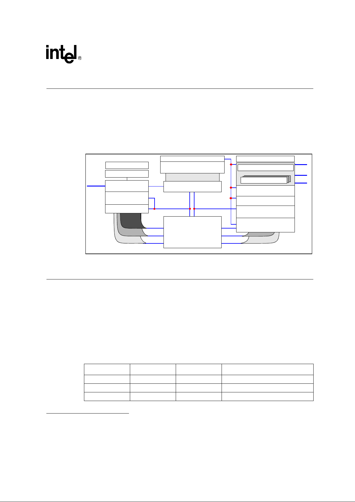
Figure 1. 80960Hx Block Diagram
Execution Unit
Programmable
Bus Controller
Bus Request Queues
Six-Port Register File
32-bit Base Bus
Instruction Cache
128-Bit Cache Bus
Instruction Prefetch Queue
Interrupt Controller
Control
Address
Data
Memory-Side
Machine Bus
Register-Side
Machine Bus
Memory Region Configuration
Multiply/Divide Unit
Interrupt
Port
AddressGeneration Unit
Data Cache
16 Kbyte,Four-WaySet-Associative
8 Kbyte,Four-WaySet-Associative
Guarded Memory Unit
Timers
JTAG Port
Parallel Instruction Scheduler
Data RAM - 2 Kbyte
RegisterCache-5to15sets
64-bit SRC1 Bus
64-bit SRC2 Bus
64-bit DST Bus
128-bit Load Bus
128-bit Store Bus
Table 1. 80960Hx Product Description
Product Core Voltage Operating Frequency (bus/core)
80960HA 1x 3.3 V
*
25/25, 33/33, 40/40
80960HD 2x 3.3 V
*
16/32, 25/50, 33/66, 40/80
80960HT 3x 3.3 V
*
20/60, 25/75
*Processor inputs are 5 V tolerant.

80960HA/HD/HT
2 Advance Information Datasheet
In addition to expanded clock frequency options, the 80960Hx provides essential enhancements for
an emerging class of high-performance embedded applications. Features include a larger
instruction cache, data cache, and data RAM than any other 80960 processor to date. It also boasts
a 32-bit demultiplexed and p ipelined burst bus, fast interrupt mechanism, guarded memory unit,
wait state generator,dual programmable timers, ONCE and IEEE 1149.1-compliant boundary scan
test and debug support, and new instructions.
2.1 The i960®Processor Family
The i960 processor family is a 32-bit RISC architecture created by Intel to serve the needs of
embedded applications. The embedded m arket includes applications as diverse as industrial
automation, avionics, image processing, graphics and communications.
Because all members of the i960 processor family share a common core architecture, i960
applications are code-compatible. Each new processor in the family adds its own special set of
functions to the core to satisfy the needs of a specific application or range of applications in the
embedded market.
2.2 Key 80960Hx Features
2.2.1 Execution Architecture
Independent instruction paths inside the processor allow the execution of multiple, out-of-sequence
instructions per clock. Register and resource scoreboarding interlocks maintain the logical integrity
of sequential instructions that are being executed in parallel. To sustain execution of multiple
instructions in each clock cycle, the processor decodes multiple instructions in parallel and
simultaneously issues these instructions to parallel processing units. The various processing units
are then able to independently access instruction operands in parallel from a common register set.
Local Register Cache integrated on-chip provides automatic register management on call/return
instructions. Upon a call instruction, the processor allocates a set of local registers for the called
procedure, then stores the registers for the previous procedure in the on-chip register cache. As
additional procedures are called, the cache stores the associated registers such that the most recently
called procedure is the first available by the nextreturn (ret) instruction. The processor can store up to
fifteen register sets, after which the oldest sets are stored (spilled) into external memory.
The 80960Hx supports the 80960 architecturally-defined branch prediction mechanism. This
allows many branches to execute with no pipeline break. With the 80960Hx’s efficient pipeline, a
branch can take as few as zero clocks to execute. The maximum penalty for an incorrect prediction
is two core clocks.
2.2.2 Pipelined, Burst Bus
A 32-bit high performance bus controller interfaces the 80960Hx core to the external memory and
peripherals. The Bus Control Unit features a maximum transfer rate of 160 Mbytes per second (at a
40 MHz external bus clock frequency). A key advantage of this design is its versatility. The user
can independently program the p hysical and logical attributes of system memory. Physical
attributes include wait state profile, bus width, and parity. Logical attributes include cacheability
and Big or Little Endian byte order. Internally programmable wait states and 16 separately
configurable physical memory regions allow the processor to interface with a variety of memory

80960HA/HD/HT
Advance Information Datasheet 3
subsystems with minimum system complexity.To reduce the effect of wait states, t he bus design is
decoupled from the core. This lets the processor execute instructions while the bus performs
memory accesses independently.
The Bus Controller’s key features include:
• Demultiplexed, Burs t Bus to support most efficient DRAM access modes
• Address Pipelining to reduce memory cost while maintaining performance
• 32-, 16- and 8-bit modes to facilitate I/O interfacing
• Full internal wait state generation to reduce system cost
• Little and Big Endian support
• Unaligned Access support implemented in hardware
• Three-deep request queue to decouple the bus from the core
• Independent physical and logical address space characteristics
2.2.3 On-Chip Caches and Data RAM
As shown in Figure 1, the 80960Hx provides generous on-chip cache and storage features to
decouple CPU execution from the external bus. The processor includes a 16 Kbyte instruction
cache, an 8 Kbyte data cache and 2 Kbytes of Data RAM. The caches are organized as 4-way set
associative. Stores that hit the data cache are written through to memory. The data cache performs
write allocation on cache misses. A fifteen-set stack frame cache allows the processor to rapidly
allocate and deallocate local registers. All of the on-chip RAM sustains a 4-word (128-bit) access
every clock cycle.
2.2.4 Priority Interrupt Controller
The interrupt unit provides the mechanism for the low latency and high throughput interrupt
service essential for embedded applications. A priority interrupt controller provides full
programmability of 240 interrupt sources with a typical interrupt task switch (latency) time of 17
core clocks. The controller supports 31 priority levels. Interru pts are prioritized and signaled within
10 core clocks of the request. If the interrupt has a higher priority than the processor priority, the
context switch to the interrupt routine would typically complete in another 7 bus clocks.
External agents post interr upts via the 8-bit external interrupt port. The Interrupt unit also handles
the two internal sources from the Timers. Interrupts can be level- or edge-triggered.
2.2.5 Guarded Memory Unit
The Guarded Memory Unit (GMU) provides memory protection without the address translation
found in Memory Management Units. The GMU contains two memory protection schemes: one
prevents illegal memory accesses, the other detects memory access violations. Both signal a fault
to the processor. The programmable protection modes are: user read, write or execute; and
supervisor read, write or execute.
80960HA/HD/HT
4 Advance Information Datasheet
2.2.6 Dual Programmable Timers
The processor provides two independent 32-bit timers, with four programmable clock rates. The
user configures the timers via the Timer Unit registers. These registers are memory-mapped within
the 80960Hx, addressable on 32-bit boundaries. The timers have a single-shot mode and
auto-reload capabilities for continuous operation. Each timer has an independent interrupt request
to the processor’s interrupt controller.
2.2.7 Processor Self Test
When a system error is detected, the FAIL pin is asserted, a fail code message is driven onto the
address bus, and the processor stops execution at the point of failure. The only way to resume
normal operation is to perform a RESET operation. Because System Error generation can occur
sometime after the bus confidence test and even after initialization during normal processor
operation, the FAIL
pin is HIGH (logic “1”) before the detection of a System Error.
The processor uses only one read bus-transaction to signal the fail code message; the address of the
bus transaction is the fail code itself. The fail code is of the form: 0xfeffffnn; bits 6 to 0 contain a
mask recording the possible failures. Bit 7, when set to 1, indicates that the mask contains failures
from the internal Built-In Self-Test (BIST); when 0, the mask indicates other failures.
Ignore reserved bits 0 and 1. Also ignore bits 5 and 6 when bit 7 is clear (=0).
The mask is shown in Table 2 and Table 3.
Table 2. Fail Codes For BIST (bit 7 = 1)
Bit When Set:
6 On-chip Data-RAM failure detected by BIST.
5 Internal Microcode ROM failure detected by BIST.
4 Instruction cache failure detected by BIST.
3 Data cache failure detected by BIST.
2 Local-register cache or processor core failure detected by BIST.
1 Reserved. Always zero.
0 Reserved. Always zero.
Table 3. Remaining Fail Codes (bit 7 = 0)
Bit When Set:
6 Reserved. Always one.
5 Reserved. Always one.
4 A data structure within the IMI is not aligned to a word boundary.
3 A System Error dur ing normal operation has occurred.
2 The Bus Confidence test has failed.
1 Reserved. Always zero.
0 Reserved. Always zero.

80960HA/HD/HT
Advance Information Datasheet 5
2.3 Instruction Set Summary
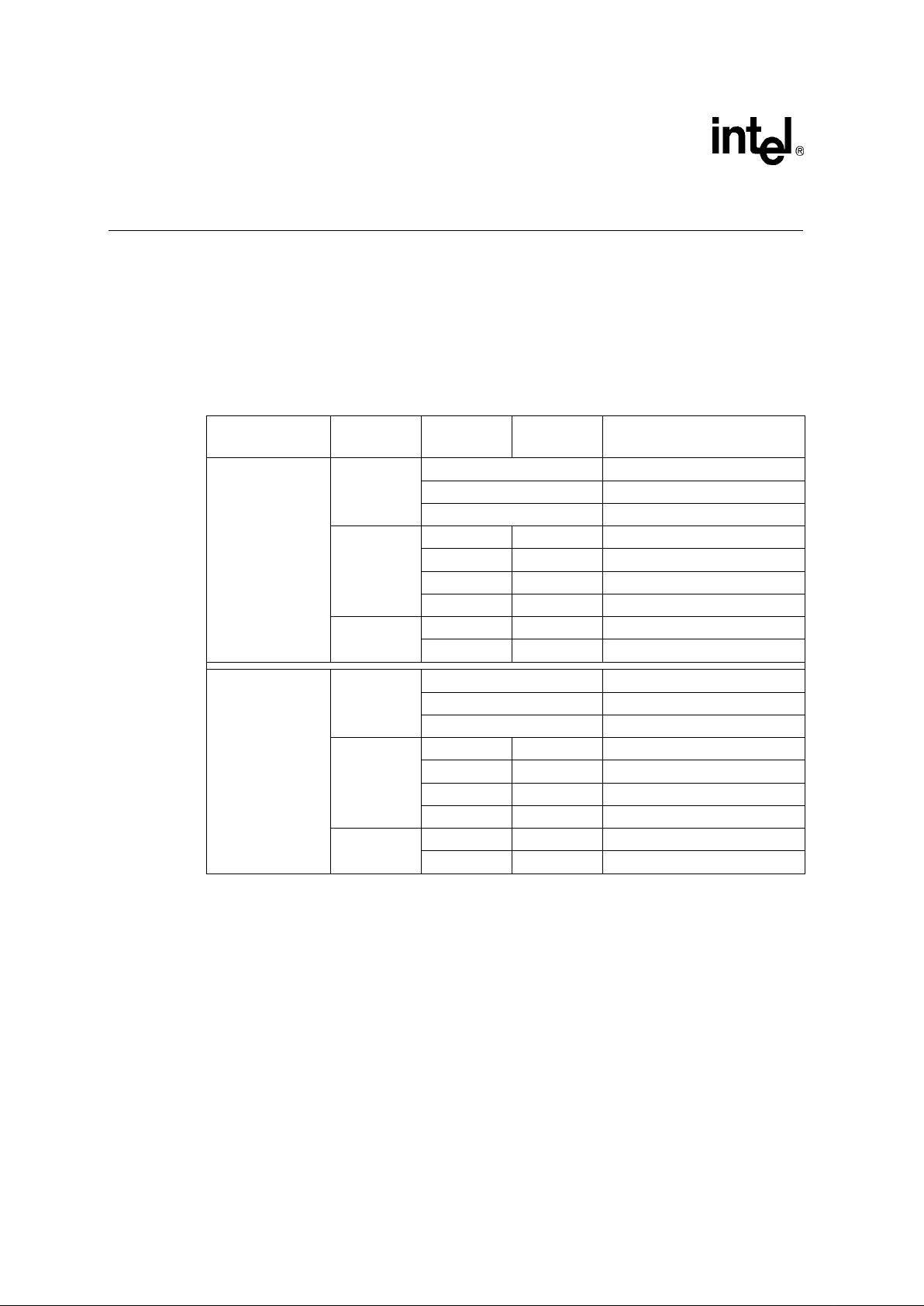
Table 4 summarizes the 80960Hx instruction set by logical groupings.
Table 4. 80960Hx Instruction Set
Data Movement Arithmetic Logical Bit / Bit Field / Byte
Load
Store
Move
Load Address
Conditional Select
(2)
Add
Subtract
Multiply
Divide
Remainder
Modulo
Shift
Extended Shift
Extended Multiply
Extended Divide
Add with Carry
Subtract with Carry
Rotate
Conditional Add
(2)
Conditional Subtract
(2)
And
Not And
And Not
Or
Exclusive Or
Not Or
Or Not
Nor
Exclusive Nor
Not
Nand
Set Bit
Clear Bit
Not Bit
Alter Bit
Scan For Bit
Span Over Bit
Extract
Modify
Scan Byte for Equal
Byte Swap
(2)
Comparison Branch Call/Return Fault
Compare
Conditional Compare
Compare and Increment
Compare and Decrement
Compare Byte
(2)
Compare Short
(2)
Test Condition C ode
Check Bit
Unconditional Branch
Conditional Branch
Compare and Branch
Call
Call Extended
Call System
Return
Branch and Link
Conditional Fault
Synchronize Faults
Debug Processor Mgmt Atomic Cache Control
Modify TraceControls
Mark
Force Mark
Flush Local Registers
Modify Arithmet ic
Controls
Modify Process Controls
Interrupt Enable/
Disable
(1,2)
System Control
(1)
Atomic Add
Atomic Modify
Instruction Cache
Control
(1,2)
Data Cache Control
(1,2)
NOTES:
1. 80960Hx extensions to the 80960 core instruction set .
2. 80960Hx extensions to the 80960Cx instruction set.
80960HA/HD/HT
6 Advance Information Datasheet
3.0 Package Information
This section describes the pins, pinouts and thermal characteristics for the 80960Hx i n the 168-pin
ceramic Pin Grid Array (PGA) package, 208-pin PowerQuad2* (PQ4). For complete package
specifications and information, see the Intel Packaging Handbook (Order# 240800).
The 80960HA/HD/HT is offered with eigth speeds and two package types (Table 5). Both the
168-pin ceramic Pin Grid Array (PGA) and the 208-pin PowerQuad2* (PQ4) devices are specified
for operation at V
CC
= 3.3 V ± 0.15 V over a case temperature range of 0° to 85°C.
Table 5. 80960HA/HD/HT Package Types and Speeds
Package/Name Devi ce
Core Speed
(MHz)
Bus Speed
(MHz)
Order #
168L PGA
80960HA
25 A80960HA25 S L2GX
33 A80960HA33 S L2GY
40 A80960HA40 S L2GZ
80960HD
32 16 A80960HD32 S L2GG
50 25 A80960HD50 S L2GH
66 33 A80960HD66 S L2GJ
80 40 A80960HD80 S L2GK
80960HT
60 20 A80960HT60
75 25 A80960HT75 S L2GP
208L PQFP
(alsoknownasPQ4)
80960HA
25 FC80960HA25 S L2GU
33 FC80960HA33 S L2GV
40 FC80960HA40 S L2GW
80960HD
32 16 FC80960HD32 S L2GL
50 25 FC80960HD50 S L2GM
66 33 FC80960HD66 S L2GN
80 40 FC80960HD80 S L2LZ
80960HT
60 20 FC80960HT60 S L2G 2
75 25 FC80960HT75 S L2GT

80960HA/HD/HT
Advance Information Datasheet 7
3.1 Pin Descriptions
This section defines the 80960Hx pins. Table 6 presents the legend for interpreting the pin
descriptions in Table 7. All pins float while the processor is in the ONCE mode, except TDO,
which can be driven active according to normal JTAG specifications.
Table 6. Pin Description Nomenclature
Symbol Description
I Input only pin.
O Output only pin.
I/O Pin can be input or output.
- Pin must be connected as indicated for proper device functionality.
S(E)
Synchronous edge sensitive input. This in put must meet the setup and hold times relative to
CLKIN to ensure p roper operation of the process o r.
S(L)
Synchronous level sensitive input. This input must meet the setup and hold times relative to
CLKIN to ensure p roper operation of the process o r.
A(E) Asynchronous edge-sensitive input.
A(L) Asynchronous level-sensitive input.
H(...)
While the processor bus is in the HOLD state (HOLDA asserted), the pin:
H(1) is driven to V
CC
H(0) is driven to V
SS
H(Z) floats
H(Q) continues to be a valid output
B(...)
While the processor is in the bus backoff state (BOFF
asserted), the pin:
B(1) is driven to V
CC
B(0) is driven to V
SS
B(Z) floats
B(Q) continues to be a valid output
R(...)
While the processor’s RESET
pin is asserted, t he pin:
R(1) is driven to V
CC
R(0) is driven to V
SS
R(Z) floats
R(Q) continues to be a valid output
80960HA/HD/HT
8 Advance Information Datasheet
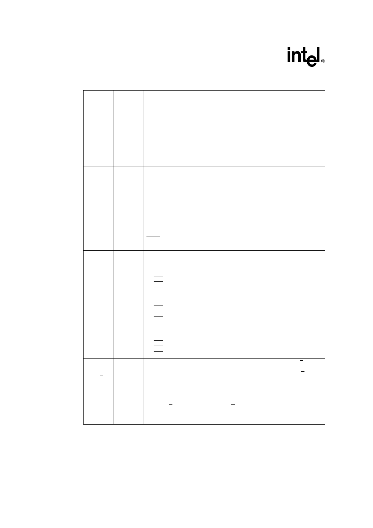
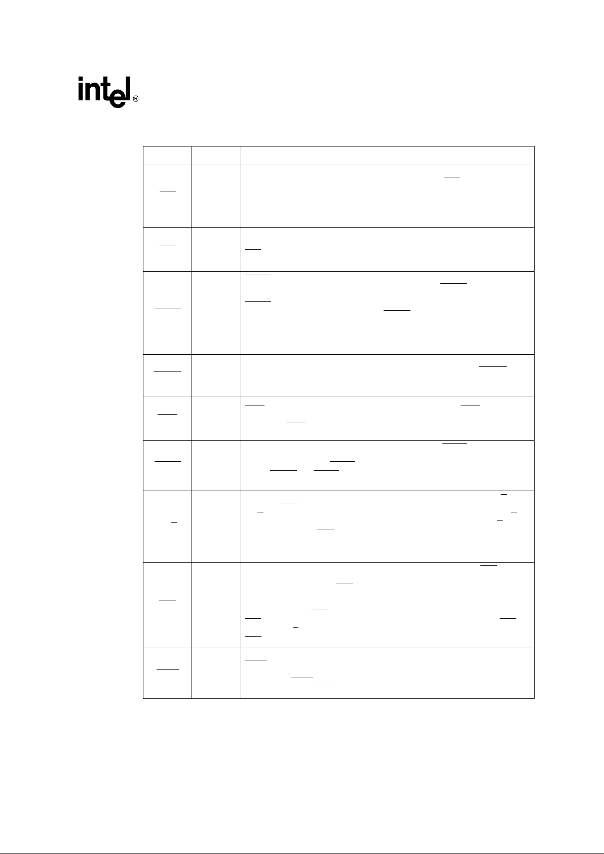
Table 7. 80960Hx Processor Family Pin Descriptions (Sheet 1 of 4)
Name Type Description
A31:2
O
H(Z)
B(Z)
R(Z)
ADDRESS BUS carries the upper 30 bits of the physical address. A31 is the most
significant address bit and A2 is the least significant. During a bus access, A31:2
identify all external addresses to word (4-byte) boundaries. The byte enable
signals indicate the selected byte in each word. During burst accesses, A3 and A2
increment to indicate successive addresses.
D31:0
I/O
S(L)
H(Z)
B(Z)
R(Z)
DATA BUS carries 32, 16, or 8-bit data quantities depending on bus wid th
configuration. The least significant bit of the data is carried on D0 and the most
significant on D31. The lower 8 data lines (D7:0) are used when the bus is
configured for 8-bit data. When configured for 16-bit data, D15:0 are used.
DP3:0
I/O
S(L)
H(Z)
B(Z)
R(Z)
DATA PARITY carries parity information for the data bus. Each parity bit is
assigned a group of 8 data bus pins as follows:
DP3 generates/checks parity for D31:24
DP2 generates/checks parity for D23:16
DP1 generates/checks parity for D15:8
DP0 generates/checks parity for D7:0
Parity information is generated for a processor write cycle and is checked for a
processor read cycle. Parity checking and polarity are programmable. Parity
generation/checking is only performed for the size of the data accessed.
PCHK
O
H(Q)
B(Q)
R(1)
PARITY CHECK indicat es the result of a parity check operation. An asserted
PCHK
indicates that the previous bus read access resulted in a parity check error.
BE3:0
O
H(Z)
B(Z)
R(1)
BYTE ENABLES select which of the four bytes addressed by A31:2 are active
during a bus access. Byte enable encoding is dependent on the bus width of the
memory region accessed:
32-bit bus:
BE3 enables D31:24
BE2
enables D23:16
BE1
enables D15:8
BE0
enables D7:0
16-bit bus:
BE3 becomes Byte High Enable (enables D15:8)
BE2
is not used (state is undefined)
BE1
becomes Address Bit 1 (A1)
BE0
becomes Byte Low Enable (enables D7:0)
8-bit bus:
BE3 is not used (state is undefined)
BE2
is not used (state is undefined)
BE1
Address Bit 1 (A 1)
BE0
Address Bit 0 (A 0)
W/R
O
H(Z)
B(Z)
R(0)
WRITE/READ is low for read accesses and high for write accesses. W/R
becomes valid during the address phase of a bus cycle and remains validuntil the
end of the cycle for non-pipelined accesses. For pipelined accesses, W/R
changes state when the next address is presented.
0= Read
1= Write
D/C
O
H(Z)
B(Z)
R(0)
DATA/CODE indicates that a bus access is a data access or an instruction
access. D/C
has the same timing as W/R.
0 = Code
1=Data
80960HA/HD/HT
Advance Information Datasheet 9
SUP
O
H(Z)
B(Z)
R(1)
SUPERVISORACCESS indicates whether the c urrent bus access originates from
a request issued while in supervisor mode or user mode. S UP
canbeusedbythe
memory subsystem to isolate supervisor code and data structures from
non-supervisor access.
0 = Supervisor Mode
1 = User Mode
ADS
O
H(Z)
B(Z)
R(1)
ADDRESS STROBE indicates a valid address and the start of a new bus access.
ADS
is asserted for the first clock of a bus access.
READY
I
S(L)
READY
, when enabled for a memory region, is asserted by the memory
subsystem to indicate the completion of a data transfer. READY
is used to
indicate that read data on the bus is valid, or that a wr ite transfer has completed.
READY
works in conjunction with the internal wait state generator to
accommodate various memory speeds. READY
is sampled after any programmed
wait states:
During each data c ycle of a burst access
During the data cycle of a non-burst access
BTERM
I
S(L)
BURST TERMINATE, when enabled for a memory r egion, is asserted by the
memory subsystem to terminate a burst access in progress. When BTERM
is
asserted, the current burst access is terminated and another address cycle
occurs.
WAIT
O
H(Z)
B(Z)
R(1)
WAIT
indicates the status of the inter nal wait-state generator. WAIT is asserted
when the internal wait state generator generates N
WAD,NRAD,NWDD
and N
RDD
wait states. WAIT canbeusedtoderiveawritedatastrobe.
BLAST
O
H(Z)
B(Z)
R(1)
BURST LAST indicates the last transfer i n a bus access. BLAST
is asserted in t he
last data transfer of burst and non-burst accesses after the internal wait-state
generator reaches zero. B LAST
remains active as long as wait states are inserted
via the READY
pin. BLAST becomes inactive after the final data transfer in a bus
cycle.
DT/R
O
H(Z)
B(Z)
R(0)
DATA TRANSMIT/RECEIVE indicates direction for data transceivers. DT/R
is
used with DEN
to provide control for data transceivers connected to the data bus.
DT/R
is driven low to indicate the processor expects data (a read cycle). DT/R is
driven high when the processor is “transmitting” data (a s tore cycle). DT/R
only
changes state when DEN
is high.
0 = Data Receive
1 = Data Transmit
DEN
O
H(Z)
B(Z)
R(1)
DATA ENABLE indicates data transfer cycles during a bus access. DEN
is
asserted at the start of the first data cycle in a bus access and de-asserted at the
end of the last data cycle. DEN
remains asserted for an entire bus request, even
when that request spans several bus accesses. For example, a l dq instruction
starting at an unaligned quad word boundary is one bus request spanning at least
two bus accesses. DEN
remains asserted throughout all the accesses (including
ADS
states) and de-asserts when the Iqd instruction request is satisfied. DE N is
used with DT/R
to provide control for data transceivers co nnected to the data bus.
DEN
remains asserted for sequential reads from pipelined memory regions.
LOCK
O
H(Z)
B(Z)
R(1)
BUS LOCK indicates that an atomic read-modify-write operation is in progress.
LOCK
may be used by the memory subsystem to prevent external agents from
accessing memory that is currently involved in an atomic operation (e.g., a
semaphore). LOCK
is asserted in the first clock of an atomic operation and
de-asserted when BLAST
is deasserted in the last bus cycle.
Table 7. 80960Hx Processor Family Pin Descriptions (Sheet 2 of 4)
Name Type Description

80960HA/HD/HT
10 Advance Information Datasheet
HOLD
I
S(L)
HOLD REQUEST signals that an external agent requests access to the
processor’s address, data, and control buses. When HOLD is asserted, the
processor:
Completes the current bus request.
Asserts HOLDA and flo ats the addres s, data, and control buses.
When HOLD is deasserted, the HOLDA pin i s deasserted and the processor
reassumes control of the address, data, and control pins.
HOLDA
O
H(1)
B(0)
R(Q)
HOLD ACKNOWLEDGE indicates to an external master that the processor has
relinquished control of the bus. The processor grants HOLD requests and enters
the HOLDA state while the RESET
pin is asserted.
HOLDA is never granted while LOCK
is asserted.
BOFF
I
S(L)
BUS BACKOFF forces the processor to immediately relinquish control of the bus
on the next clock cycle. When READY
/BTERM is enabled and:
When BOFF
is asserted, the address, data, and control buses are floated on the
next clock cycle and the current ac cess is aborted.
When BOFF
is deasserted, the processor resumes by regenerating the aborted
bus access.
See Figure 16 on page 40 for BOFF
timing requirements.
BREQ
O
H(Q)
B(Q)
R(0)
BUS REQUEST indicates that a bus request is pending in the bus controller.
BREQ does not indicate whether or not the processor is stalled. See BSTALL for
processor stall status. BREQ can be used with BSTALL to indicate to an external
bus arbiter the processor’s bus ownership requirements.
BSTALL
O
H(Q)
B(Q)
R(0)
BUS STALL indicates that the processor has stalled pending the result of a
request in the bus controller. When BSTALL is asserted, the processor must
regain bus ow nership to continue processing (i.e., it can no longer execute strictly
out of on-chip cache memory).
CT3:0
O
H(Z)
B(Z)
R(Z)
CYCLE TYPE indicates the type of bus cycle currently being started or processor
state. CT3:0 encoding follows:
Cycle Type ADSCT3:0
Program-initiated access using 8-bit bus 00000
Program-initiated access using 16-bit bus 00001
Program-initiated access using 32-bit bus 00010
Event-initiated access using 8-bit bus 00100
Event-initiated access using 16-bit bus 00101
Event-initiated access using 32-bit bus 00110
Reserved 00X11
Reserved for future products 01XXX
Reserved 1XXXX
XINT7:0
I
A(E)
A(L)
EXTERNAL INTERRUPT pins are us e d to r equest interrupt service. These pins
can be configured in three modes:
Dedicated Mode:
Each pin is assigned a dedicated interrupt level. Dedicated
inputs can be programmed to be level (low or high) or edge (rising or falling)
sensitive.
Expanded Mode:
All eight pins act as a vectored interrupt source. The interrupt
pins are level sensitive in this mode.
Mixed Mode:
The XINT7:5pins act as dedicated sources and the XINT4:0 pins act
as the five most significant bits of a vectored source. The least significant bits of
the vectored source are set to “010” internally.
NMI
I
A(E)
NON-MASKABLE INTERRUPT causes a non-maskable interrupt event to occur.
NMI
is the highest priority interrupt source. NMI is falling edge triggered.
Table 7. 80960Hx Processor Family Pin Descriptions (Sheet 3 of 4)
Name Type Description
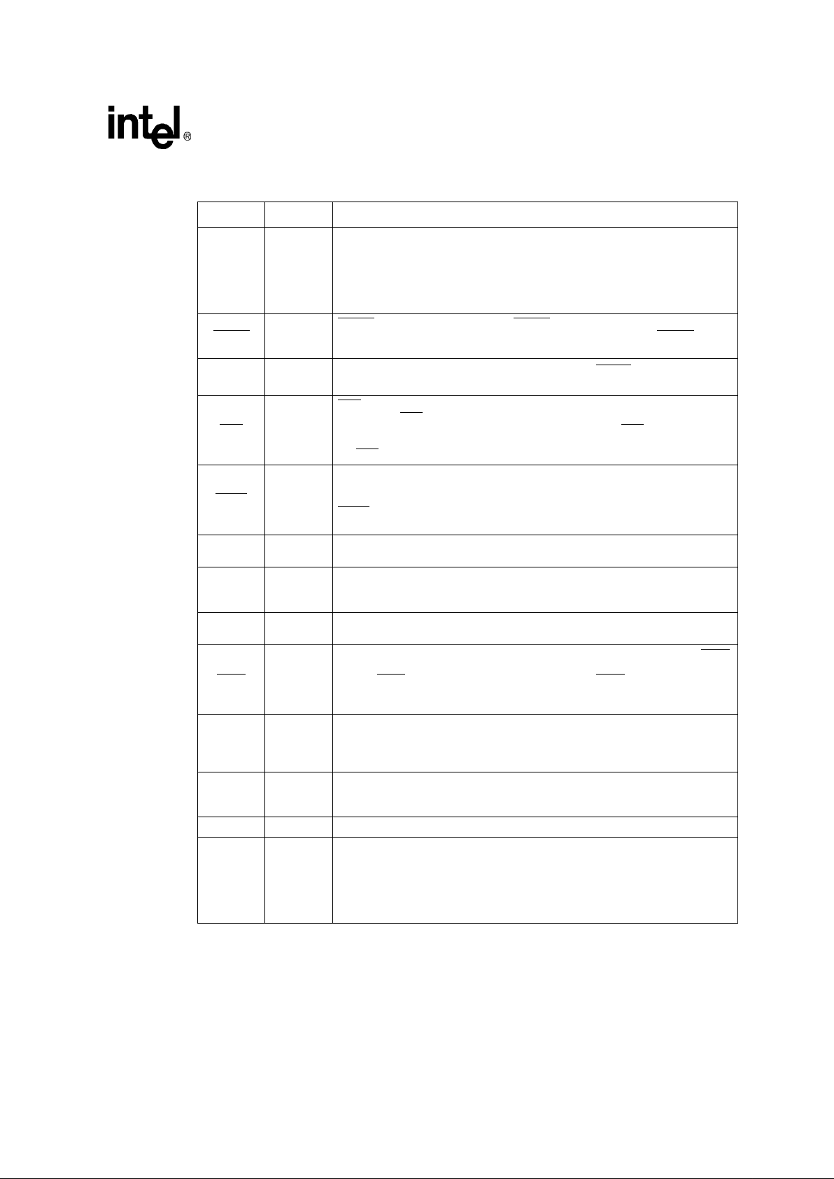
80960HA/HD/HT
Advance Information Datasheet 11
CLKIN I
CLOCK INPUT provides the time base for the 80960Hx. A ll internal circuitry is
synchronized to CLKIN. All input and output timings are specified relative to
CLKIN.
For the 80960HD, the 2x internal clock is derived by multiplying the CLKIN
frequency by 2. For the 80960HT, the 3x inter nal clock is derived by multiplying
the CLKIN frequency by 3.
RESET
I
A(L)
RESET
forces the device into reset. RESET causes all external and internal
signals to return to their reset state ( if defined). The rising edge of RESET
starts
the processor boot sequenc e.
STEST
I
S(L)
SELF TEST, when asserted during the rising edge of RESET
, causes the
processor to execute its built in self-test.
FAIL
O
H(Q)
B(Q)
R(0)
FAIL
indicates a failure of the processor’s built-in self-test performed during
initialization. FAIL
is assert ed immediately out of reset and togg les during self-test
to indicate the status of individual tests. If self-test passes, FAIL
is de-asserted
and the processor branches to the user’s initialization code. When self-test fails,
the FAIL
pin asserts and the processor ceases execution.
ONCE
I
ON-CIRCUIT EMULATIONcontrol: the processor samples this pin during reset. If
it is asserted low at the end of reset, the processor enters ONCE mode. In ONCE
mode, the processor stops all clocks and floats all output pins except the TDO pin.
ONCE
uses an internal pull-up resistor; see RPUdefinition in Table 21 “80960Hx
DC Characteri stics” on page 32. Pull this pin high when not in use.
TCK I
TEST CLOCK provides the clocking function for IEEE 1149.1 Boundar y Scan
testing.
TDI I
TEST DATA INPUT is the serial input pin for I EE E 1149.1 Boundar y Scan testing.
TDI uses an internal pull-up resistor; see R
PU
definition in Table 21 “80960Hx DC
Characteristics” on page 32.
TDO O
TEST DATA OUTPUT is the serial output pin for IEEE 1149.1 Boundary Scan
testing. ONCE does not disable this pin.
TRST
I
TEST RESET asynchronously resets the TestAccess Port (TAP)controller.TRS T
must be held low at least 10,000 clock cycles after power-up. One method is to
provide TRST
with a separate power-on-reset circuit. TRST includes an internal
pull-up resistor ; see R
PU
definition in Table21 “80960Hx DC Characteristics” on
page 32. Pull this pin low when not in use.
TMS I
TEST MODE SELECT is sampled at the rising edge of TCK. TCK controls the
sequence of TAP controller state changes for IEEE 1149.1 Boundary Scan
testing. TMS uses an internal pull-up resistor; see R
PU
definition in Ta ble 21
“80960Hx DC Characteristics” on page 32.
VCC5 I
5 V REFERENCE VOLTAGE input is the reference voltage for the 5 V-tolerant I/O
buffers. Connect t his signal to +5 V for use with inputs which exceed 3.3 V. When
all inputs are from 3.3 V components, connect this signal to 3.3 V.
VCCPLL I PLL VOLTAGE is the +3.3 VDC analog input for the PLL.
VOLDET O
VOLTAGE DETECT signal allows external system logic to distinguish between a
5 V 80960Cx processor and the 3.3 V 80960Hx processor. This signal is active
low for a 3.3 V 80960Hx (it is high impedance for 5 V 80960Cx). This pin is
available only on the PGA version.
0 = 80960Hx
1 = 80960Cx
Table 7. 80960Hx Processor Family Pin Descriptions (Sheet 4 of 4)
Name Type Description
80960HA/HD/HT
12 Advance Information Datasheet
3.2 80960Hx Mechanical Data
3.2.1 80960Hx PGA Pinout
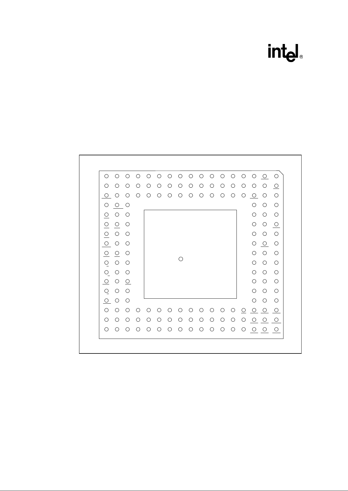
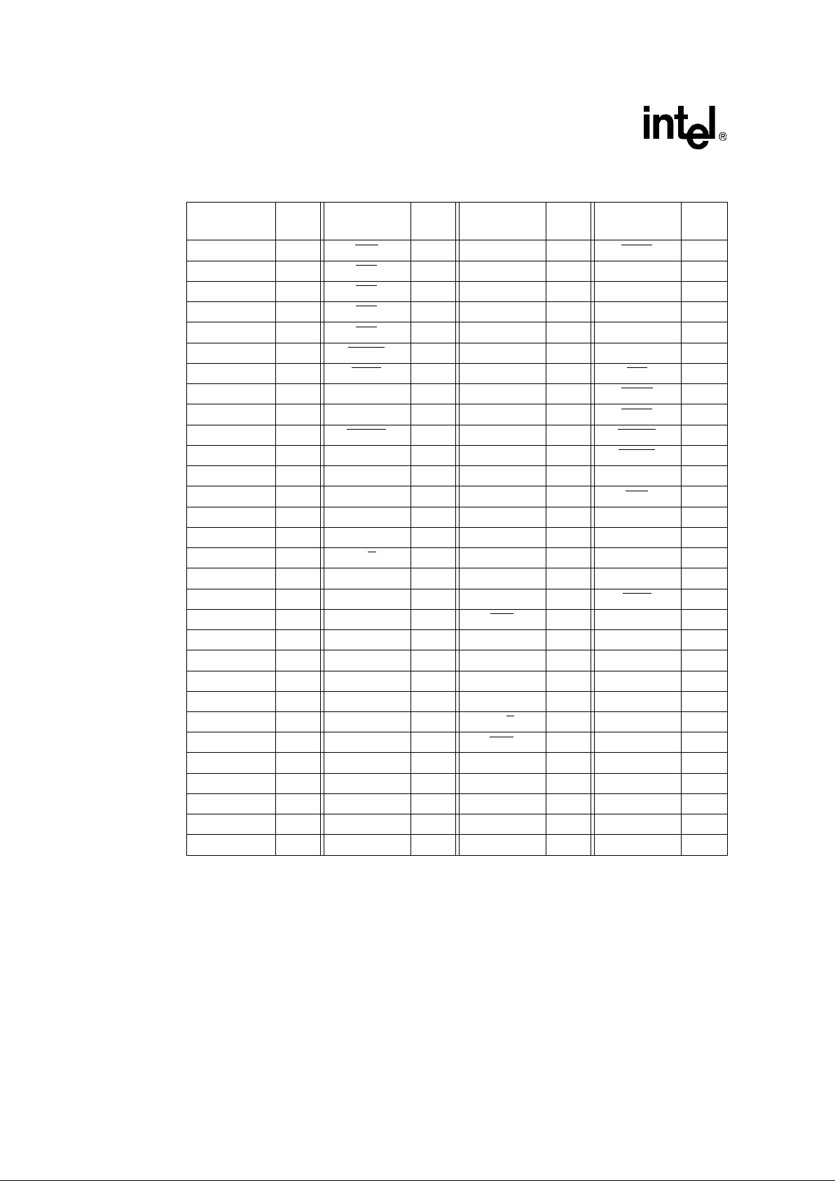
Figure 2 depicts the complete 80960Hx PGA pinout as viewed from the top side of the component
(i.e., pins facing down). Figure 3 shows the complete 80960Hx PGA pinout as viewed from the
pin-side of the package (i.e., pins facing up). Table 9 lists the 80960Hx pin names with package
location. See Section 4.3, “Recommended Connections” on page 30 for specifications and
recommended connections.
Figure 2. 80960Hx 168-Pin PGA Pinout — View from Top (Pins Facing Down)
D5D7D8D9D11D12D13D15D16D17D19D21D24D25
D2D4D6V
CC
D10V
CC
V
CC
D14V
CC
D18D20D23D27D29
NCD0V
CC
V
SS
V
SS
V
SS
V
SS
V
SS
V
SS
V
CC
D22D31READY D26
D28BTERM
HOLDA
D30HOLD
BE3
V
CC
ADSBE2
V
SS
V
CC
BE1
V
SS
V
CC
BLAST
V
SS
BE0DEN
V
SS
V
CC
W/R
V
SS
V
CC
DT/R
A29LOCK
SUPWAIT BSTALL
A28
A30BREQD/C
D3
D1
ONCE
V
SS
VCC5
V
CC
V
SS
V
SS
V
SS
V
SS
V
SS
CLKIN
V
CC
V
SS
BOFF
STEST
DP1
DP3
TCK
TMS
V
CC
PCHK
V
CC
VCCPLL
V
CC
NC
NC
V
CC
V
SS
FAIL
DP0
DP2
VOLDET
TRST
TDI
TDO
NC
NC
CTO
CT2
CT3
CT1
V
SS
A2
V
CC
A22A25
A20 V
SS
A3A5
NMI
V
CC
V
SS
V
SS
V
SS
VSSV
SS
A24A31 A26
A4V
CC
A6A8A9A10A11A12A14A15A17A18
V
CC
V
CC
V
CC
A13V
CC
A16A19A21A23A27 A7
XINT6
XINT7
XINT4
XINT3
XINT5
XINT0
RESET
XINT2
XINT1
1
2
3
4
5
6
7
8
9
10
11
12
13
14
15
16
17
1
2
3
4
5
6
7
8
9
10
11
12
13
14
15
16
17
ABCDEFGHJKLMNPQRS
ABCDEFGHJKLMNPQRS
i
© 19xx
A80960Hx
XXXXXXXX SS
M

80960HA/HD/HT
Advance Information Datasheet 13
Figure 3. 80960Hx 168-Pin PGA Pinout — View from Bottom (Pins Facing Up)
D5 D7 D8 D9 D11 D12 D13 D15 D16 D17 D19 D21 D24 D25
D2 D4 D6 V
CC
D10 VCCVCCD14 VCCD18 D20 D23 D27 D29
NC D0 V
CCVSSVSSVSSVSSVSSVSSVCC
D22 D31 READYD26
D28 BTERM
HOLDA
D30 HOLD BE3
VCCADS BE2
VSSVCCBE1
VSSVCCBLAST
V
SS
BE0 DEN
VSSVCCW/R
VSSVCCDT/R
A29 LOCK
SUP WAITBSTALL
A28
A30 BREQ D/C
D3
D1
ONCE
V
SS
VCC5
V
CC
V
SS
V
SS
V
SS
V
SS
V
SS
CLKIN
V
CC
V
SS
BOFF
STEST
DP1
DP3
TCK
TMS
V
CC
PCHK
V
CC
VCCPLL
V
CC
NC
NC
V
CC
V
SS
FAIL
DP0
DP2
VOLDET
TRST
TDI
TDO
NC
NC
CT0
CT2
CT3
CT1
V
SS
A2
V
CC
A22 A25
A20V
SS
A3 A5
NMI
VCCV
SS
VSSV
SS
V
SS
V
SS
A24 A31A26
A4 V
CC
A6 A8 A9 A10 A11 A12 A14 A15 A17 A18
V
CCVCCVCC
A13 VCCA16 A19 A21
A23
A27A7XINT6
XINT7
XINT4
XINT3
XINT5
XINT0
RESET
XINT2
XINT1
1
2
3
4
5
6
7
8
9
10
11
12
13
14
15
16
17
1
2
3
4
5
6
7
8
9
10
11
12
13
14
15
16
17
ABCDEFGHJKLMNPQRS
ABCDEFGHJKLMNPQRS
Package Lid
80960HA/HD/HT
14 Advance Information Datasheet
Table 8. 80960Hx 168-Pin PGA Pinout — Signal Name Order (Sheet 1 of 2)
Signal Name
PGA
Pin
Signal Name
PGA
Pin
Signal Name
PGA
Pin
Signal Name
PGA
Pin
A2 D16 ADS
R6 D14 L2 LOCK S14
A3 D17 BE0
R9 D15 L1 NC A9
A4 E16 BE1
S7 D16 M1 NC A10
A5 E17 BE2
S6 D17 N1 NC B13
A6 F17 BE3
S5 D18 N2 NC B14
A7 G16 BLAST
S8 D19 P1 NC D3
A8 G17 BOFF
B1 D20 P2 NMI D15
A9 H17 BREQ R13 D21 Q1 ONCE
C3
A10 J17 BSTALL R12 D22 P3 PCHK
B8
A11 K17 BTERM
R4 D23 Q2 READY S3
A12 L17 CLKIN C13 D24 R1 RESET
A16
A13 L16 CT0 A11 D25 S1 STEST B2
A14 M17 CT1 A12 D26 Q3 SUP
Q12
A15 N17 CT2 A13 D27 R2 TCK B5
A16 N16 CT3 A14 D28 Q4 TDI A7
A17 P17 D/C
S13 D29 S2 TDO A8
A18 Q17 D0 E3 D30 Q5 TMS B6
A19 P16 D1 C2 D31 R3 TRST
A6
A20 P15 D2 D2 DEN
S9 V
CC
B7
A21 Q16 D3 C1 DP0 A3 V
CC
B9
A22 R17 D4 E2 DP1 B3 V
CC
B11
A23 R16 D5 D1 DP2 A4 V
CC
B12
A24 Q15 D6 F2 DP3 B4 V
CC
C6
A25 S17 D7 E1 DT/R
S11 V
CC
C14
A26 R15 D8 F1 FAIL
A2 V
CC
E15
A27 S16 D9 G1 ——V
CC
F3
A28 Q14 D10 H2 ——V
CC
F16
A29 R14 D11 H1 ——V
CC
G2
A30 Q13 D12 J1 HOLD R5 V
CC
H16
A31 S15 D13 K1 HOLDA S4 V
CC
J2
80960HA/HD/HT
Advance Information Datasheet 15
V
CC
J16 VCCPLL B10 V
SS
H3 V
SS
Q10
V
CC
K2 VOLDET A5 V
SS
H15 V
SS
Q11
V
CC
K16 V
SS
A1 V
SS
J3 W/R S10
V
CC
M2 V
SS
C4 V
SS
J15 WAIT S12
V
CC
M16 V
SS
C7 V
SS
K3 XINT0 B15
V
CC
N3 V
SS
C8 V
SS
K15 XINT1 A15
V
CC
N15 V
SS
C9 V
SS
L3 XINT2 A17
V
CC
Q6 V
SS
C10 V
SS
L15 XINT3 B16
V
CC
R7 V
SS
C11 V
SS
M3 XINT4 C15
V
CC
R8 V
SS
C12 V
SS
M15 XINT5 B17
V
CC
R10 V
SS
F15 V
SS
Q7 XINT6 C16
V
CC
R11 V
SS
G3 V
SS
Q8 XINT7 C17
VCC5 C5 V
SS
G15 V
SS
Q9 ——
Table 8. 80960Hx 168-Pin PGA Pinout — Signal Name Order (Sheet 2 of 2)
Signal Name
PGA
Pin
Signal Name
PGA
Pin
Signal Name
PGA
Pin
Signal Name
PGA
Pin
80960HA/HD/HT
16 Advance Information Datasheet
Table 9. 80960Hx 168-Pin PGA Pinout — Pin Number Order (Sheet 1 of 2)
PGA
Pin
Signal Name
PGA
Pin
Signal Name
PGA
Pin
Signal Name
PGA
Pin
Signal Name
A1 V
SS
B14 NC E15 V
CC
K15 V
SS
A2 FAIL B15 XINT0 E16 A4 K16 V
CC
A3 DP0 B16 XINT3 E17 A5 K17 A11
A4 DP2 B17 XINT5
F1 D8 L1 D15
A5 VOLDET C1 D3 F2 D6 L2 D14
A6 TRST
C2 D1 F3 V
CC
L3 V
SS
A7 TDI C3 ONCE F15 V
SS
L15 V
SS
A8 TDO C4 V
SS
F16 V
CC
L16 A13
A9 NC C5 VCC5 F17 A6 L17 A12
A10 NC C6 V
CC
G1 D9 M1 D16
A11 CT0 C7 V
SS
G2 V
CC
M2 V
CC
A12 CT1 C8 V
SS
G3 V
SS
M3 V
SS
A13 CT2 C9 V
SS
G15 V
SS
M15 V
SS
A14 CT3 C10 V
SS
G16 A7 M16 V
CC
A15 XINT1 C11 V
SS
G17 A8 M17 A14
A16 RESET
C12 V
SS
H1 D11 N1 D17
A17 XINT2
C13 CLKIN H2 D10 N2 D18
B1 BOFF
C14 V
CC
H3 V
SS
N3 V
CC
B2 STEST C15 XINT4 H15 V
SS
N15 V
CC
B3 DP1 C16 XINT6 H16 V
CC
N16 A16
B4 DP3 C17 XINT7
H17 A9 N17 A15
B5 TCK D1 D5 J1 D12 P1 D19
B6 TMS D2 D2 J2 V
CC
P2 D20
B7 V
CC
D3 NC J3 V
SS
P3 D22
B8 PCHK
D15 NMI J15 V
SS
P15 A20
B9 V
CC
D16 A2 J16 V
CC
P16 A19
B10 VCCPLL D17 A3 J17 A10 P17 A17
B11 V
CC
E1 D7 K1 D13 Q1 D21
B12 V
CC
E2 D4 K2 V
CC
Q2 D23
B13 NC E3 D0 K3 V
SS
Q3 D26
80960HA/HD/HT
Advance Information Datasheet 17
Q4 D28 Q16 A21 R11 V
CC
S6 BE2
Q5 D30 Q17 A18 R12 BSTALL S7 BE1
Q6 V
CC
R1 D24 R13 BREQ S8 BLAST
Q7 V
SS
R2 D27 R14 A29 S9 DEN
Q8 V
SS
R3 D31 R15 A26 S10 W/R
Q9 V
SS
R4 BTERM R16 A23 S11 DT/R
Q10 V
SS
R5 HOLD R17 A22 S12 WAIT
Q11 V
SS
R6 ADS S1 D25 S13 D/C
Q12 SUP R7 V
CC
S2 D29 S14 LOCK
Q13 A30 R8 V
CC
S3 READY S15 A31
Q14 A28 R9 BE0
S4 HOLDA S16 A27
Q15 A24 R10 V
CC
S5 BE3 S17 A25
Table 9. 80960Hx 168-Pin PGA Pinout — Pin Number Order (Sheet 2 of 2)
PGA
Pin
Signal Name
PGA
Pin
Signal Name
PGA
Pin
Signal Name
PGA
Pin
Signal Name

80960HA/HD/HT
18 Advance Information Datasheet
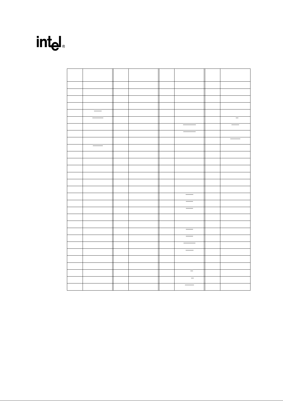
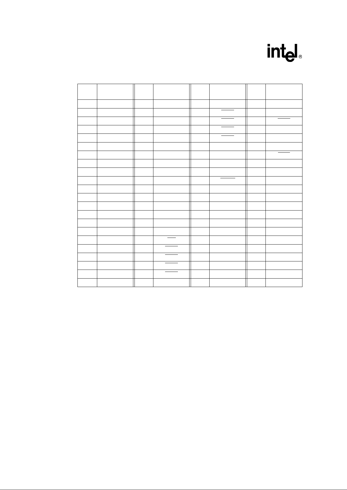
3.2.2 80960Hx PQ4 Pinout
Figure 4. 80960Hx 208-Pin PQ4 Pinout
PIN 1
PIN 208
PIN 52
PIN 53
PIN 104
PIN 157
PIN 156
V
CC
VSSV
SS
V
CC
FAI L
ONCE
V
SS
V
CC
BOFF
V
CC
D0D1D2
D3
V
SS
V
CC
V
SS
V
CC
D4D5D6
D7
V
SS
V
CC
D8
D9
D10
V
CC
V
SS
VCCD12
D13
D14
D15
VCCD16
D17
D18
D19
V
SS
VCCD21
D22
D23
PIN 105
V
SS
D24
D25
D26
D27
V
SS
V
CC
V
CC
D28
D29
D30
D31
V
SS
V
CC
BTERM
READY
HOLD
HOLDA
V
SS
V
CC
V
SS
V
CC
V
SS
V
CC
ADS
BE3
BE2
V
SS
V
CC
BE1
BE0
BLAST
DEN
V
SS
V
CC
W/R
DT/R
WAIT
BSTALL
V
CC
V
SS
V
SS
V
CC
D/C
SUP
V
SS
LOCK
BREQ
V
CC
V
CC
V
SS
VSSVSSVCCVCCVSSA2A3VCCVSSA4A5A6A7VCCVSSA8A9A10
A11
VCCVSSA12
A13
A14
A15
VCCVSSVSSVCCA16
A17
A18
A19
VCCVSSA20
A21
A22
A23
VCCVSSVCCVSSA24
A25
A26
A27
VCCVSSA28
A29
A30
V
SS
V
CC
NMI
XINT7
XINT6
XINT5
XINT4
V
SS
V
CC
XINT3
XINT2
XINT1
XINT0
V
SS
V
CC
V
SS
V
CC
RESET
CLKIN
VCCPLL
V
SS
V
CC
CT3
CT2
CT1
CT0
V
SS
V
CC
V
SS
V
CC
TDO
PCHK
V
SS
TDI
TMS
TRST
TCK
V
SS
V
CC
VCC5
V
CC
V
SS
V
CC
DP3
DP2
V
CC
V
SS
DP0
DP1
STEST
D11
V
SS
A31
V
SS
V
CC
D20
V
CC
V
SS
V
SS
i
XXXXXXXX SS
M
©19xx
i960
®
FC80960Hx
V
CC
V
SS

80960HA/HD/HT
Advance Information Datasheet 19
Table 10. 80960Hx PQ4 Pinout — Signal Name Order (Sheet 1 of 2)
Signal Name
PQ4
Pin
Signal Name
PQ4
Pin
Signal Name
PQ4
Pin
Signal Name
PQ4
Pin
A2 151 BE0
83 D16 39 PCHK 189
A3 150 BE1
82 D17 40 READY 68
A4 147 BE2
79 D18 41 RESET 174
A5 146 BE3
78 D19 42 STEST 208
A6 145 BLAST
84 D20 45 SUP 97
A7 144 BOFF
10 D21 50 TCK 194
A8 141 BREQ 100 D22 51 TDI 191
A9 140 BSTALL 91 D23 52 TDO 188
A10 139 BTERM
67 D24 54 TMS 192
A11 138 CLKIN 175 D25 55 TRST
193
A12 135 CT0 183 D26 56 V
CC
1
A13 134 CT1 182 D27 57 V
CC
4
A14 133 CT2 181 D28 61 V
CC
9
A15 132 CT3 180 D29 62 V
CC
11
A16 127 D/C
96 D30 63 V
CC
17
A17 126 D0 12 D31 64 V
CC
19
A18 125 D1 13 DEN
85 V
CC
25
A19 124 D2 14 DP0 206 V
CC
31
A20 121 D3 15 DP1 207 V
CC
33
A21 120 D4 20 DP2 203 V
CC
38
A22 119 D5 21 DP3 202 V
CC
44
A23 118 D6 22 DT/R
89 V
CC
46
A24 113 D7 23 FAIL
5 V
CC
49
A25 112 D8 26 ——V
CC
59
A26 111 D9 27 ——V
CC
60
A27 110 D10 28 ——V
CC
66
A28 107 D11 29 HOLD 69 V
CC
71
A29 106 D12 34 HOLDA 72 V
CC
74
A30 105 D13 35 LOCK
99 V
CC
76
A31 104 D14 36 NMI
159 V
CC
81
ADS
77 D15 37 ONCE 6 V
CC
87
80960HA/HD/HT
20 Advance Information Datasheet
V
CC
92 V
CC
187 V
SS
70 V
SS
164
V
CC
95 V
CC
196 V
SS
73 V
SS
170
V
CC
101 V
CC
199 V
SS
75 V
SS
172
V
CC
102 V
CC
201 V
SS
80 V
SS
178
V
CC
109 V
CC
204 V
SS
86 V
SS
184
V
CC
115 VCC5 197 V
SS
93 V
SS
186
V
CC
117 VCCPLL 177 V
SS
94 V
SS
190
V
CC
123 V
SS
2 V
SS
98 V
SS
195
V
CC
128 V
SS
3 V
SS
103 V
SS
198
V
CC
131 V
SS
7VSS108 V
SS
200
V
CC
137 V
SS
8 V
SS
114 V
SS
205
V
CC
143 V
SS
16 V
SS
116 W/R 88
V
CC
149 V
SS
18 V
SS
122 WAIT 90
V
CC
153 V
SS
24 V
SS
129 XINT0 169
V
CC
154 V
SS
30 V
SS
130 XINT1 168
V
CC
158 V
SS
32 V
SS
136 XINT2 167
V
CC
165 V
SS
43 V
SS
142 XINT3 166
V
CC
171 V
SS
47 V
SS
148 XINT4 163
V
CC
173 V
SS
48 V
SS
152 XINT5 162
V
CC
176 V
SS
53 V
SS
155 XINT6 161
V
CC
179 V
SS
58 V
SS
156 XINT7 160
V
CC
185 V
SS
65 V
SS
157 ——
Table 10. 80960Hx PQ4 Pinout — Signal Name Order (Sheet 2 of 2)
Signal Name
PQ4
Pin
Signal Name
PQ4
Pin
Signal Name
PQ4
Pin
Signal Name
PQ4
Pin
80960HA/HD/HT
Advance Information Datasheet 21
Table 11. 80960Hx PQ4 Pinout — Pin Number Order (Sheet 1 of 2)
PQ4
Pin
Signal Name
PQ4
Pin
Signal Name
PQ4
Pin
Signal Name
PQ4
Pin
Signal Name
1 V
CC
31 V
CC
61 D28 91 BSTALL
2 V
SS
32 V
SS
62 D29 92 V
CC
3 V
SS
33 V
CC
63 D30 93 V
SS
4 V
CC
34 D12 64 D31 94 V
SS
5 FAIL 35 D13 65 V
SS
95 V
CC
6 ONCE 36 D14 66 V
CC
96 D/C
7 V
SS
37 D15 67 BTERM 97 SUP
8 V
SS
38 V
CC
68 READY 98 V
SS
9 V
CC
39 D16 69 HOLD 99 LOCK
10 BOFF 40 D17 70 V
SS
100 BREQ
11 V
CC
41 D18 71 V
CC
101 V
CC
12 D0 42 D19 72 HOLDA 102 V
CC
13 D1 43 V
SS
73 V
SS
103 V
SS
14 D2 44 V
CC
74 V
CC
104 A31
15 D3 45 D20 75 V
SS
105 A30
16 V
SS
46 V
CC
76 V
CC
106 A29
17 V
CC
47 V
SS
77 ADS 107 A28
18 V
SS
48 V
SS
78 BE3 108 V
SS
19 V
CC
49 V
CC
79 BE2 109 V
CC
20 D4 50 D21 80 V
SS
110 A27
21 D5 51 D22 81 V
CC
111 A26
22 D6 52 D23 82 BE1
112 A25
23 D7 53 V
SS
83 BE0 113 A24
24 V
SS
54 D24 84 BLAST 114 V
SS
25 V
CC
55 D25 85 DEN 115 V
CC
26 D8 56 D26 86 V
SS
116 V
SS
27 D9 57 D27 87 V
CC
117 V
CC
28 D10 58 V
SS
88 W/R 118 A23
29 D11 59 V
CC
89 DT/R 119 A22
30 V
SS
60 V
CC
90 WAIT 120 A21
80960HA/HD/HT
22 Advance Information Datasheet
121 A20 143 V
CC
165 V
CC
187 V
CC
122 V
SS
144 A7 166 XINT3 188 TDO
123 V
CC
145 A6 167 XINT2 189 PCHK
124 A19 146 A5 168 XINT1 190 V
SS
125 A18 147 A4 169 XINT0 191 TDI
126 A17 148 V
SS
170 V
SS
192 TMS
127 A16 149 V
CC
171 V
CC
193 TRST
128 V
CC
150 A3 172 V
SS
194 TCK
129 V
SS
151 A2 173 V
CC
195 V
SS
130 V
SS
152 V
SS
174 RESET 196 V
CC
131 V
CC
153 V
CC
175 CLKIN 197 VCC5
132 A15 154 V
CC
176 V
CC
198 V
SS
133 A14 155 V
SS
177 VCCPLL 199 V
CC
134 A13 156 V
SS
178 V
SS
200 V
SS
135 A12 157 V
SS
179 V
CC
201 V
CC
136 V
SS
158 V
CC
180 CT3 202 DP3
137 V
CC
159 NMI 181 CT2 203 DP2
138 A11 160 XINT7
182 CT1 204 V
CC
139 A10 161 XINT6 183 CT0 205 V
SS
140 A9 162 XINT5 184 V
SS
206 DP0
141 A8 163 XINT4
185 V
CC
207 DP1
142 V
SS
164 V
SS
186 V
SS
208 STEST
Table 11. 80960Hx PQ4 Pinout — Pin Number Order (Sheet 2 of 2)
PQ4
Pin
Signal Name
PQ4
Pin
Signal Name
PQ4
Pin
Signal Name
PQ4
Pin
Signal Name

80960HA/HD/HT
Advance Information Datasheet 23
3.3 Package Thermal Specifications
The 80960Hx is specified for operation when TC(case temperature) is within the range of
0°C–85°C. T
C
may be measured in any environment to determine whether the 80960Hx is within
the specified operating range. Measure the case temperature at the center of the top surface,
opposite the pins. Refer to Figure 5.
T
A
(ambient temperature) is calculated from θCA(thermal resistance from case to ambient) using
the equation:
TA=TC–P*θ
CA
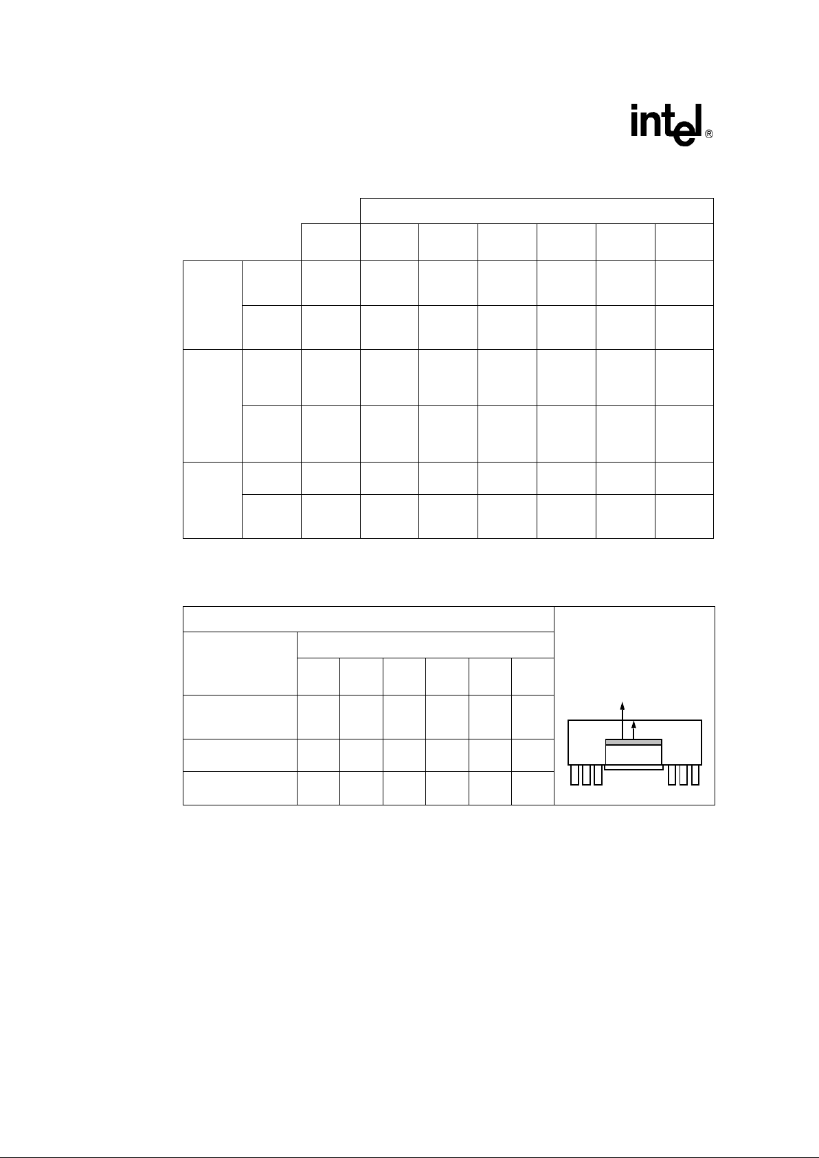
Table 12 shows the maximum TAallowable (without exceeding TC) at various airflows and
operating frequencies (f
CLKIN
).
Note that T
A
is greatly improved by attaching fins or a heatsink to the package. P (maximum power
consumption) is calculated by using the typical I
CC
as tabulated in Section 4.6, “DC
Specifications” on page 32 and V
CC
of 3.3 V.
Figure 5. Measuring 80960Hx PGA Case Temperature
Measure PGA/PQ4 temperature at
center of top surface
80960HA/HD/HT
24 Advance Information Datasheet
Table 12. Maximum T
A
at Various Airflows in °C (PGA Package Only)
Airflow-ft/min (m/sec)
f
CLKIN
(MHz)
0
(0)
200
(1.01)
400
(2.03)
600
(3.04)
800
(4.06)
1000
(5.07)
Core
1X Bus
Clock
T
A
with
Heatsink*
25
33
40
69
63
59
74
70
67
78
75
73
79
77
75
80
79
77
80
79
77
T
A
without
Heatsink
25
33
40
64
56
50
67
62
56
71
67
63
74
70
67
75
72
69
76
74
71
Core
2X Bus
Clock
T
A
with
Heatsink*
16
25
33
40
68
58
49
41
73
66
60
55
77
73
69
65
79
75
71
68
80
77
74
72
80
77
74
72
T
A
without
Heatsink
16
25
33
40
62
49
38
27
66
56
46
38
71
62
55
48
73
66
60
55
75
68
63
58
76
71
66
62
Core
3X Bus
Clock
T
A
with
Heatsink*
20
25
53
45
63
58
71
67
73
70
76
73
76
73
T
A
without
Heatsink
20
25
43
33
51
42
58
51
63
58
66
61
68
64
*0.285” high unidirectional heatsink (AI alloy 6061, 50 mil fin width, 150 mil center-to-center fin spacing).
Table 13. 80960Hx 168-Pin PGA Package Thermal Characteristics
Thermal Resistance — °C/Watt
Parameter
Airflow — ft./min (m/ sec)
0
(0)
200
(1.01)
400
(2.03)
600
(3.07)
800
(4.06)
1000
(5.07)
θ Junction-to-Case
(Case measured as
shown in Figure 5)
1.51.51.51.51.51.5
θ Case-to-Ambient
(No Heatsink)
17 14 11 9 8 7
θ Case-to-Ambient
(With Heatsink)*
1396544
NOTES:
1. This table applies to 80960Hx PGA plugged into s ocket or soldered directly to board.
2. θ
JA
= θJC+ θ
CA
*0.285” high unidirectional heatsink (AI alloy 6061, 50 mil fin width, 150 mil center-to-center fin spacing).
θ
JC
θ
JA
 Loading...