

Datasheet E28F800B5-T90, E28F800B5-T70, E28F800B5-B90, E28F800B5-B70 Datasheet (Intel Corporation)

E
PRODUCT PREVIEW
December 1996 Order Number: 290599-003
n
SmartVoltage Technology
Smart 5 Flash: 5V Reads,
5V or 12V Writes
Increased Programming Throughput
at 12V V
PP
n
Very High-Performance Read
2-, 4-Mbit: 60 ns Access Time
8-Mbit: 70 ns Access Time
n
x8/x16-Configurable Input/Output Bus
n
Low Power Consumption
Max 60 mA Read Current at 5V
Auto Power Savings: <1 mA Typical
Standby Current
n
Optimized Array Blocking Architecture
16-KB Protected Boot Block
Two 8-KB Parameter Blocks
96-KB and 128-KB Main Blocks
Top or Bottom Boot Locations
n
Extended Temperature Operation
–40°C to +85°C
n
Industry-Standard Packaging
44-Lead PSOP, 48-Lead TSOP
n
Extended Block Erase Cycling
100,000 Cycles at Commercial Temp
10,000 Cycles at Extended Temp
n
Hardware Data Protection Feature
Absolute Hardware-Protection for
Boot Block
Write Lockout during Power
Transitions
n
Automated Word/Byte Program and
Block Erase
Command User Interface
Status Registers
Erase Suspend Capability
n
SRAM-Compatible Write Interface
n
Reset/Deep Power-Down Input
Provides Low-Power Mode and
Reset for Boot Operations
n
Pinout Compatible 2, 4, and 8 Mbit
n
ETOX™ Flash Technology
0.6 µ ETOX IV Initial Production
0.4 µ ETOX V Later Production
Intel’s word-wide Smart 5 boot bloc k flash memory family provides 2-, 4-, and 8-Mbit memories featuring
high-density, low-cost, nonvolatile, read/write storage solutions for a wide range of applications. Their
asymmetrically-blocked architecture, flexible voltage, and extended cycling provide highly flexible
components suitable for em bedded code exec ution applic ations, suc h as network ing inf rastruct ure and offic e
automation.
Based on Intel’s boot bloc k archit ecture, the word-wide Sm art 5 boot bloc k memory family enables quic k and
easy upgrades for designs that demand state-of-the-art technology. This family of products comes in
industry-standard packages: the 48-lead TSOP, ideal for board-constrained applications, and the rugged,
easy to handle 44-lead PSOP.
SMART 5 BOOT BLOCK
FLASH MEMORY FAMILY
2, 4, 8 MBIT
28F200B5, 28F400B5, 28F800B5

Information in this document is provided in connection with Intel products. No license, express or implied, by estoppel or
otherwise, to any intellectual property rights is granted by this document. Except as provi ded in Intel ’s Terms and Condi tions of
Sale for such products, Intel assumes no liability whatsoever, and Intel disclaims any express or implied warranty, relating to
sale and/or use of Intel products including liability or warranties relating to fitness for a particular purpose, merchantability, or
infringement of any patent, copyright or other intellectual property right. Intel products are not intended for use in medical, life
saving, or life sustaining applications.
Intel may make changes to specifications and product descriptions at any time, without notice.
The 28F200B5, 28F400B5, 28F800B5 may contain design defects or errors known are errata. Current characterized errata are
available on request.
*Third-party brands and names are the property of their respective owners.
Contact your local Intel sales office or your distributor to obtain the latest specifications and before placing your product order.
Copies of documents which have an ordering number and are referenced in this document, or other Intel literature, may be
obtained from:
Intel Corporation
P.O. Box 7641
Mt. Prospect, IL 60056-7641
or call 1-800-879-4683
COPYRIGHT © INTEL CORPORATION, 1996 CG-041493

E SMART 5 BOOT BLOCK MEMORY FAMILY
3
PRODUCT PREVIEW
CONTENTS
PAGE PAGE
1.0 INTRODUCTION.............................................5
1.1 New Features in the Smart 5 Memory
Products .....................................................5
1.2 Product Overview ........................................5
2.0 PRODUCT DESCRIPTION..............................6
2.1 Pin Descriptions...........................................6
2.2 Pinouts.........................................................8
2.3 Memory Blocking Organization ..................10
2.3.1 Boot Block........................................... 10
2.3.2 Parameter Blocks................................ 10
2.3.3 Main Blocks.........................................10
3.0 PRINCIPLES OF OPERATION..................... 13
3.1 Bus Operations..........................................13
3.1.1 Read...................................................13
3.1.2 Output Disable ....................................14
3.1.3 Standby...............................................14
3.1.4 Word/Byte Configuration.....................14
3.1.5 Deep Power-Down/Reset....................14
3.1.6 Write ................................................... 14
3.2 Modes of Operation ...................................16
3.2.1 Read Array.......................................... 16
3.2.2 Read Identifier.....................................16
3.2.3 Read Status Register.......................... 16
3.2.4 Word/Byte Program.............................17
3.2.5 Block Erase......................................... 17
3.3 Boot Block Locking ....................................24
3.3.1 V
PP
= VIL for Complete Protection....... 24
3.3.2 WP# = V
IL
for Boot Block Locking .......24
3.3.3 RP# = V
HH
or WP# = VIH for Boot Block
Unlocking...........................................24
3.3.4 Note for 8-Mbit 44-PSOP Package...... 24
4.0 DESIGN CONSIDERATIONS........................24
4.1 Power Consumption...................................24
4.1.1 Active Power.......................................24
4.1.2 Automatic Power Savings (APS) .........24
4.1.3 Standby Power....................................25
4.1.4 Deep Power-Down Mode.....................25
4.2 Power-Up/Down Operation.........................25
4.2.1 RP# Connected To System Reset.......25
4.3 Board Design.............................................25
4.3.1 Power Supply Decoupling....................25
4.3.2 V
PP
Trace On Printed Circuit Boards...25
5.0 SPECIFICATIONS.........................................26
5.1 Absolute Maximum Ratings........................26
5.2 Test Conditions..........................................26
5.3 Operating Conditions .................................27
5.4 Reset Operations.......................................27
5.6 Electrical Specifications .............................28
DC Characteristics Table...........................28
AC Characteristics: Read Operations
Table........................................................30
AC Characteristics: Write Operations
Table........................................................32
Erase and Program Timings ......................34
APPENDIX A: Ordering Information.................35
APPENDIX B: Write State Machine: Current-
Next State Chart..........................................36
APPENDIX C: Product Block Diagram .............37
APPENDIX D: Additional Information...............38

SMART 5 BOOT BLOCK MEMORY FAMILY E
4
PRODUCT PREVIEW
REVISION HISTORY
Number Description
-001 Original Version
-002 Minor changes throughout document.
Section 3.1.5 and Figure 13 redone to clarify program/erase operation abort.
Information added to Table 2, Figure 1, and Section 3.3 to clarify WP# on 8-Mbit,
44-PSOP.
Read and Write Waveforms changed to numbered format.
Typical numbers removed from DC Characteristics and Erase/Program Timings.
-003 Minor text changes throughout document.
Figure 1, 44-PSOP pinout: mistake on pin 3 on 2-Mbit pinout corrected from A
17
to NC.
Specs t
EHQZ
and t
GHQZ
improved.
Explanations of program/erase abort commands reworked in Table 6, Command
Codes.
E SMART 5 BOOT BLOCK MEMORY FAMILY
5
PRODUCT PREVIEW
1.0 INTRODUCTION
This datasheet contains specifications for 2-, 4-,
and 8-Mbit Smart 5 boot block flash memories.
Section 1 provides a feature overview. Sections 2,
3, and 4 describe the product and functionality.
Section 5 details the electrical and timing
specifications for both commercial and extended
temperature operation.
1.1 New Features in the
Smart 5 Memory Products
The Smart 5 boot block flas h memory fami ly of fers
identical features with the BV/CV/BE/CE
SmartVoltage products, except the Smart 5 boot
block -B5 parts only support 5V V
CC
read voltage.
The following differences dist inguish the Smart 5
boot block products from their predecessors:
• A delay is required if the part i s reset during an
in-progress program or erase operation.
• On the fly word-byte mode switching is no
longer supported. Word-byte mode must be
configured at power-up and remain stable
during operation.
• Write operations are no longer specified as
WE#- or CE#-controlled in favor of a simpler
“unified” write method, which is compatible
with either of the old methods.
1.2 Product Overview
The word-wide Smart 5 boot block memory family
provides pinout-compatible f lash memories at the
2-, 4- and 8-Mbit densities. The 28F200B5,
28F400B5, and 28F800B5 can be configured to
operate either in 16-bit or 8-bit bus mode, wit h the
data divided into individually erasable blocks.
Table 1. Smart 5 Boot Block Family: Feature Summary
Feature 28F200B5 28F400B5 28F800B5 Reference
VCC Read Voltage 5V ± 5%, 5V ± 10% Table 10
VPP Prog/Erase Voltage 5V ± 10% or 12V ± 5%, auto-detected Table 10
Bus-width 8- or 16-bit configurable Table 2
Speed (ns) Commercial 60, 80 60, 80 70, 90 Table 14
Extended 80 80 90 Table 14
Memory Arrangement x8: 256K x 8
x16: 128K x 16
x8: 512K x 8
x16: 256K x 16
x8: 1M x 8
x16: 512K x 16
Blocking
(Top or Bottom boot
locations available)
1 x 16k Boot Block
2 x 8k Parameter
1 x 96k Main Block
1 x 128k Main Block
1 x 16k Boot Block
2 x 8k Parameter
1 x 96k Main Block
3 x 128k Main Block
1 x 16k Boot Block
2 x 8k Parameter
1 x 96k Main Block
7 x 128k Main Block
Sect. 2.3,
Fig. 3-6
Locking Boot Block lockable using WP# and/or RP#
All others protectable using V
PP
switch
Sect. 3.3
Operating Temperature Commercial: 0°C – +70 °C
Extended: -40°C – +85 °C
Table 10
Erase Cycling 100,000 cycles at Commercial Temperature
10,000 cycles at Extended Temperature
Packages 44-PSOP, 48-TSOP Figs. 1-2

SMART 5 BOOT BLOCK MEMORY FAMILY E
6
PRODUCT PREVIEW
SmartVoltage technology enables fast factory
programming and low-power designs. Specifically
designed for 5V systems, Smart 5 components
support read operations at 5V V
CC
and internally
configure to program/erase at 5V or 12V . The 12V
V
PP
option renders the fastest program and erase
performance which will increase your factory
throughput. With the 5V V
PP
option, VCC and V
PP
can be tied together for a simple 5V design. In
addition, the dedicated V
PP
pin gives complete dat a
protection when V
PP
≤ V
PPLK
.
The memory array is asymmetrically divided into
blocks in an asymmetrical architecture to
accommodate microprocessors that boot from the
top (denoted by -T suffix ) or the bottom (-B suffix)
of the memory map. The blocks include a
hardware-lockable boot block (16,384 bytes), two
parameter blocks (8,192 bytes each) and main
blocks (one block of 98,304 bytes and additional
block(s) of 131,072 bytes). See Figures 3–6 for
memory maps. Each block can be independently
erased and programmed 100,000 times at
commercial temperature or 10,000 times at
extended temperature. Unlike erase operations,
which erase all locations within a block
simultaneously, each byte or word in the flash
memory can be programmed independentl y of other
memory locations.
The hardware-lockable boot block provides
complete code security for the k ernel code required
for system initialization. Locking and unlocking of
the boot block is controlled by WP# and/or RP#
(see Section 3.3 for details).
The system processor interfaces to the flash device
through a Command User Interface (CUI), using
valid command sequences to initiate device
automation. An internal Wri te State Machine (WSM)
automatically executes the algorithms and timings
necessary for program and erase operations. The
Status Register (SR) indicates the status of the
WSM and whether it successfully completed the
desired program or erase operation.
The Automatic Power Savings (APS) feature
substantially reduces active current when the
device is in stati c mode (addresses not switching).
In APS mode, the typical I
CCR
current is 1 mA.
When CE# and RP# pins are at V
CC
, the
component enters a CMOS s tandby mode. Driving
RP# to GND enables a deep power-down mode
which significantly reduces power consumption,
provides write protection, resets the device, and
clears the status register. A reset time (t
PHQV
) is
required from RP# switching high until output s are
valid. Likewise, t he device has a wake time (t
PHEL
)
from RP#-high until writes to the CUI are
recognized. See Section 4.2.
The deep power-down mode can also be used as a
device reset, allowing the flash to be reset along
with the rest of the system. For example, when the
flash memory powers-up, it automatically defaults
to the read array mode, but during a warm system
reset, where power continues uninterrupted to the
system components, the flash memory could
remain in a non-read mode, such as erase.
Consequently, the system Reset signal should be
tied to RP# to reset the memory to normal read
mode upon activation of the Res et signal. Thi s also
provides protection against unwanted command
writes due to invalid system bus conditions during
system reset or power-up/down sequences.
These devices are configurable at power-up for
either byte-wide or word-wide input/output using the
BYTE# pin. Please see Table 2 for a detailed
description of BYTE# operations, especially the
usage of the DQ
15/A–1
pin.
These Smart 5 memory products are available in
the 44-lead PSOP (Plasti c Small Outline P ackage),
which is ROM/EPROM-com patible, and the 48-lead
TSOP (Thin Small Outline Pack age, 1.2 mm thick)
as shown in Figure 1, and 2, respectively.
2.0 PRODUCT DESCRIPTION
This section describes the pinout and block
architecture of the device family.
2.1 Pin Descriptions
The pin descriptions table details t he usage of eac h
of the device pins.

E SMART 5 BOOT BLOCK MEMORY FAMILY
7
PRODUCT PREVIEW
Table 2. Pin Descriptions
Symbol Type Name and Function
A0–A
18
INPUT
ADDRESS INPUTS for memory addresses. Addresses are internally latched
during a write cycle.
28F200: A[0-16], 28F400: A[0-17], 28F800: A[0-18]
A
9
INPUT ADDRESS INPUT: When A9 is at VHH the signature mode is accessed. During
this mode, A
0
decodes between the manufacturer and device IDs. When BYTE#
is at a logic low, only the lower byte of the signatures are read. DQ
15/A–1
is a
don’t care in the signature mode when BYTE# is low.
DQ0–DQ
7
INPUT/
OUTPUT
DATA INPUTS/OUTPUTS: Inputs array data on the second CE# and WE# cycle
during a Program command. Inputs commands to the Command User Interface
when CE# and WE# are active. Data is internally latched during the write cycle.
Outputs array, Intelligent Identifier and Status Register data. The data pins float to
tri-state when the chip is de-selected or the outputs are disabled.
DQ8–DQ
15
INPUT/
OUTPUT
DATA INPUTS/OUTPUTS: Inputs array data on the second CE# and WE# cycle
during a Program command. Data is internally latched during the write cycle.
Outputs array data. The data pins float to tri-state when the chip is de-selected or
the outputs are disabled as in the byte-wide mode (BYTE# = “0”). In the byte-wide
mode DQ
15/A–1
becomes the lowest order address for data output on DQ0–DQ7.
CE# INPUT CHIP ENABLE: Activates the device’s control logic, input buffers, decoders and
sense amplifiers. CE# is active low. CE# high de-selects the memory device and
reduces power consumption to standby levels. If CE# and RP# are high, but not
at a CMOS high level, the standby current will increase due to current flow
through the CE# and RP# input stages.
OE# INPUT OUTPUT ENABLE: Enables the device’s outputs through the data buffers during
a read cycle. OE# is active low.
WE# INPUT WRITE ENABLE: Controls writes to the Command Register and array blocks.
WE# is active low. Addresses and data are latched on the rising edge of the WE#
pulse.
RP# INPUT RESET/DEEP POWER-DOWN: Uses three voltage levels (VIL, VIH, and VHH) to
control two different functions: reset/deep power-down mode and boot block
unlocking. It is backwards-compatible with the BX/BL/BV products.
When RP# is at logic low, the device is in reset/deep power-down mode,
which puts the outputs at High-Z, resets the Write State Machine, and draws
minimum current.
When RP# is at logic high, the device is in standard operation. When RP#
transitions from logic-low to logic-high, the device defaults to the read array mode.
When RP# is at V
HH
, the boot block is unlocked and can be programmed or
erased. This overrides any control from the WP# input.

SMART 5 BOOT BLOCK MEMORY FAMILY E
8
PRODUCT PREVIEW
Table 2. Pin Descriptions (Continued)
Symbol Type Name and Function
WP# INPUT WRITE PROTECT: Provides a method for unlocking the boot block with a logic
level signal in a system without a 12V supply.
When WP# is at logic low, the boot block is locked, preventing program and
erase operations to the boot block. If a program or erase operation is attempted
on the boot block when WP# is low, the corresponding status bit (bit 4 for
program, bit 5 for erase) will be set in the Status Register to indicate the operation
failed.
When WP# is at logic high, the boot block is unlocked and can be
programmed or erased.
NOTE: This feature is overridden and the boot block unlocked when RP# is at
V
. This pin can not be left floating. Because the 8-Mbit 44-PSOP package does
not have enough pins, it does not include this pin and thus 12V on RP# is
required to unlock the boot block. See Section 3.3 for details on write protection.
BYTE# INPUT BYTE# ENABLE: Configures whether the device operates in byte-wide mode (x8)
or word-wide mode (x16). This pin must be set at power-up or return from deep
power-down and not changed during device operation. BYTE# pin must be
controlled at CMOS levels to meet the CMOS current specification in standby
mode.
When BYTE# is at logic low, the byte-wide mode is enabled, where data is
read and programmed on DQ
0
–DQ7 and DQ15/A–1 becomes the lowest order
address that decodes between the upper and lower byte. DQ
8
–DQ14 are tri-stated
during the byte-wide mode.
When BYTE# is at logic high, the word-wide mode is enabled, where data is
read and programmed on DQ
0
–DQ15.
V
CC
DEVICE POWER SUPPLY: 5.0V ± 10%
V
PP
PROGRAM/ERASE POWER SUPPLY: For erasing memory array blocks or
programming data in each block, a voltage either of 5V ± 10% or 12V ± 5% must
be applied to this pin. When V
PP
< V
PPL
K
all blocks are locked and protected
against Program and Erase commands.
GND GROUND: For all internal circuitry.
NC NO CONNECT: Pin may be driven or left floating.
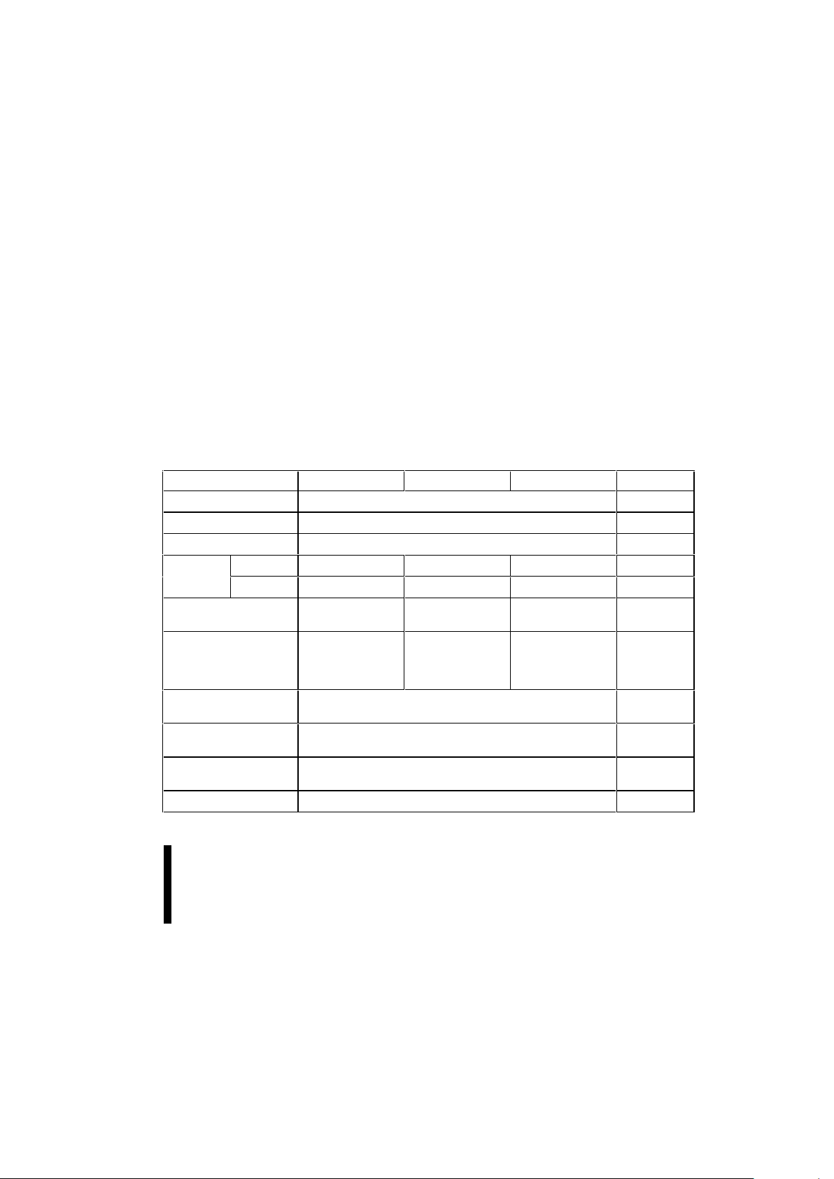
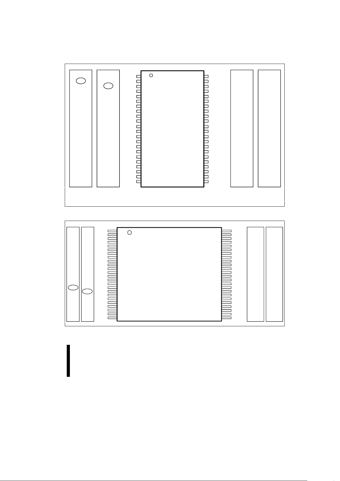
2.2 Pinouts
Intel’s Smart 5 boot block architecture provides
upgrade paths in each package pinout up to the
8-Mbit density. The 44-lead PSOP pinout follows
the industry-standard ROM/EPROM pinout, as
shown in Figure 1. Designs with space concerns
should consider the 48-lead pinout shown in
Figure 2.
Pinouts for the corresponding 2-, 4- and 8-Mbit
components are provided on the same di agram for
convenient reference. 2-Mbit pinouts are given on
the chip illustration in the center, with 4-Mbit and
8-Mbit pinouts going outward from the center.
E SMART 5 BOOT BLOCK MEMORY FAMILY
9
PRODUCT PREVIEW
PA28F200
Boot Block
44-Lead PSOP
0.525" x 1.110"
TOP VIEW
GND
WE#
RP#
BYTE#
A
8
A
9
A
11
A
12
A
13
A
14
A
16
DQ
7
DQ
14
DQ
6
DQ
13
DQ
12
DQ
4
V
CC
DQ
5
A
10
A
15
32
31
30
29
28
27
26
25
24
23
33
34
35
36
37
38
39
40
41
42
43
44
22
21
20
19
17
18
1
2
3
4
5
6
7
8
9
10
11
12
13
14
16
15
28F400 28F400
DQ
15 -1
/A
CE#
GND
OE#
V
PP
28F800 28F800
A
17
A
7
A
6
A
5
A
4
A
3
A
2
A
1
A
0
DQ
0
DQ
8
DQ
1
DQ
9
DQ
2
DQ
10
DQ
3
DQ
11
A
18
CE#
GND
OE#
V
PP
A
17
A
7
A
6
A
5
A
4
A
3
A
2
A
1
A
0
DQ
0
DQ
8
DQ
1
DQ
9
DQ
2
DQ
10
DQ
3
DQ
11
WP#
CE#
GND
OE#
V
PP
NC
A
7
A
6
A
5
A
4
A
3
A
2
A
1
A
0
DQ
0
DQ
8
DQ
1
DQ
9
DQ
2
DQ
10
DQ
3
DQ
11
WP#
GND
WE#
RP#
BYTE#
A
8
A
9
A
11
A
12
A
13
A
14
A
16
DQ
7
DQ
14
DQ
6
DQ
13
DQ
12
DQ
4
V
CC
DQ
5
A
10
A
15
DQ
15 -1
/A
GND
WE#
RP#
BYTE#
A
8
A
9
A
11
A
12
A
13
A
14
A
16
DQ
7
DQ
14
DQ
6
DQ
13
DQ
12
DQ
4
V
CC
DQ
5
A
10
A
15
DQ
15 -1
/A
0599-01
NOTE: Pin 2 is WP# on 2- and 4-Mbit devices but A18 on the 8-Mbit because no other pins were available for the high order
address. Thus, the 8-Mbit in 44-PSOP cannot unlock the boot block without RP# = VHH. See Section 3.3 for details. To allow
upgrades to 8-Mbit from 2/4-Mbit in this package design pin 2 to control WP# at the 2/4-Mbit level and A18 at the 8-Mbit density.
Figure 1. 44-Lead PSOP Pinout Diagram
28F200
Boot Block
48-Lead TSOP
12 mm x 20 mm
TOP VIEW
33
34
35
36
37
38
39
40
41
42
43
44
45
46
47
48
24
23
22
21
20
19
17
18
1
2
3
4
5
6
7
8
9
10
11
12
13
14
16
15
25
26
27
28
29
30
31
32
CE#
OE#
GND
A
0
V
CC
GND
BYTE#
A
16
DQ
15
/A
-1
DQ
7
DQ
14
DQ
6
DQ
13
DQ
5
DQ
12
DQ
4
DQ
11
DQ
10
DQ
2
DQ
9
DQ
1
DQ
8
DQ
0
DQ
3
CE#
OE#
GND
A
0
V
CC
GND
BYTE#
A
16
DQ
15
/A
-1
DQ
7
DQ
14
DQ
6
DQ
13
DQ
5
DQ
12
DQ
4
DQ
11
DQ
10
DQ
2
DQ
9
DQ
1
DQ
8
DQ
0
DQ
3
CE#
OE#
GND
A
0
V
CC
GND
BYTE#
A
16
DQ
15
/A
-1
DQ
7
DQ
14
DQ
6
DQ
13
DQ
5
DQ
12
DQ
4
DQ
11
DQ
10
DQ
2
DQ
9
DQ
1
DQ
8
DQ
0
DQ
3
28F400 28F80028F40028F800
RP#
WE#
NC
NC
NC
WP#
A
15
A
14
A
13
A
12
A
11
A
10
A
9
A
8
V
PP
A
17
A
6
A
7
A
4
A
5
A
3
A
2
RP#
WE#
NC
NC
NC
WP#
A
15
A
14
A
13
A
12
A
11
A
10
A
9
A
8
V
PP
A
6
A
7
A
4
A
5
A
3
A
2
RP#
WE#
NC
NC
NC
WP#
A
18
A
15
A
14
A
13
A
12
A
11
A
10
A
9
A
8
V
PP
A
17
A
6
A
7
A
4
A
5
A
3
A
2
NC
NC
NC
1
A
1
A
1
A
0599-02
Figure 2. 48-Lead TSOP Pinout Diagram

SMART 5 BOOT BLOCK MEMORY FAMILY E
10
PRODUCT PREVIEW
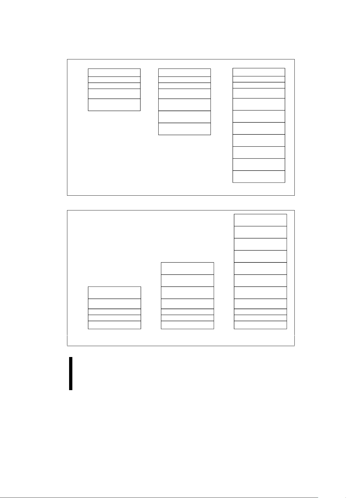
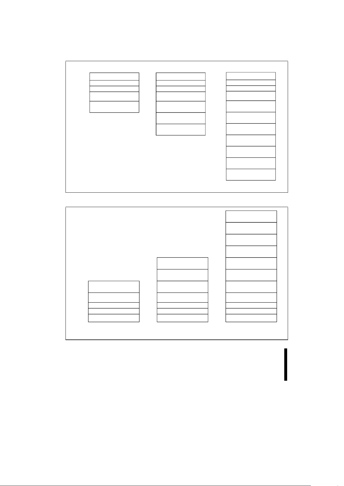
2.3 Memory Blocking Organization
The boot block product family features an
asymmetrically-blocked architecture providing
system memory integration. Each erase block can
be erased independently of the others up to
100,000 times for commerc ial temperature or up to
10,000 times for extended tem perature. The block
sizes have been chosen to optimize their
functionality for common appli cations of nonvolatile
storage. The combination of block sizes in the boot
block architecture allow the integration of several
memories into a single chip. For the address
locations of the blocks, see the memory maps in
Figures 3, 4, 5 and 6.
2.3.1 ONE 16-KB BOOT BLOCK
The boot block is intended to repl ace a dedicated
boot PROM in a microprocess or or microcontrollerbased system. The 16-Kbyte (16,384 bytes) boot
block is located at either the top (denoted by -T
suffix) or the bottom (-B suffix) of the address m ap
to accommodate different microproces sor protocols
for boot code location. This boot block features
hardware controllable write-protection to protec t the
crucial microprocessor boot code from accidental
modification. The protection of the boot block is
controlled using a combinati on of the V
PP
, RP#, and
WP# pins, as is detailed in Section 3.3.
2.3.2 TWO 8-KB PARAMETER BLOCKS
Each boot block component c ontains two parameter
blocks of 8 Kbytes (8,192 bytes) each to facilitate
storage of frequently updated s mall param eters t hat
would normally require an EEPROM. By using
software techniques, the byte-rewrite functionality
of EEPROMs can be emulated. These tec hniques
are detailed in Intel’s application note,
AP-604
Using Intel’s Boot B lock Flash Memory Parameter
Blocks to Replace EEPROM
. The parameter blocks
are not write-protectable.
2.3.3 MAIN BLOCKS - ONE 96-KB +
ADDITIONAL 128-KB BLOCKS
After the allocation of address space to the boot
and parameter blocks, the remainder is divided into
main blocks for data or code storage. Each device
contains one 96-Kbyte (98,304 byte) block and
additional 128-Kbyte (131,072 byte) blocks. The
2-Mbit has one 128-KB block; the 4-M bit , t hree; and
the 8-Mbit, seven.
E SMART 5 BOOT BLOCK MEMORY FAMILY
11
PRODUCT PREVIEW
128-Kbyte MAIN BLOCK
8-Kbyte PARAMETER BLOCK
16-Kbyte BOOT BLOCK
8-Kbyte PARAMETER BLOCK
96-Kbyte MAIN BLOCK
128-Kbyte MAIN BLOCK
128-Kbyte MAIN BLOCK
128-Kbyte MAIN BLOCK
128-Kbyte MAIN BLOCK
128-Kbyte MAIN BLOCK
128-Kbyte MAIN BLOCK
00000H
0FFFFH
10000H
1FFFFH
20000H
2FFFFH
30000H
3FFFFH
40000H
4FFFFH
50000H
5FFFFH
60000H
6FFFFH
70000H
7BFFFH
7C000H
7CFFFH
7D000H
7DFFFH
7E000H
7FFFFH
28F800-T
128-Kbyte MAIN BLOCK
8-Kbyte PARAMETER BLOCK
16-Kbyte BOOT BLOCK
8-Kbyte PARAMETER BLOCK
96-Kbyte MAIN BLOCK
128-Kbyte MAIN BLOCK
128-Kbyte MAIN BLOCK
00000H
0FFFFH
10000H
1FFFFH
20000H
2FFFFH
30000H
3BFFFH
3C000H
3CFFFH
3D000H
3DFFFH
3E000H
3FFFFH
28F400-T
128-Kbyte MAIN BLOCK
8-Kbyte PARAMETER BLOCK
16-Kbyte BOOT BLOCK
8-Kbyte PARAMETER BLOCK
96-Kbyte MAIN BLOCK
00000H
0FFFFH
10000H
1BFFFH
1C000H
1CFFFH
1D000H
1DFFFH
1E000H
1FFFFH
28F200-T
0599-03
NOTE: Word addresses shown.
Figure 3. Word-Wide x16-Mode Memory Maps (Top Boot)
128-Kbyte MAIN BLOCK
8-Kbyte PARAMETER BLOCK
16-Kbyte BOOT BLOCK
8-Kbyte PARAMETER BLOCK
96-Kbyte MAIN BLOCK
128-Kbyte MAIN BLOCK
128-Kbyte MAIN BLOCK
128-Kbyte MAIN BLOCK
128-Kbyte MAIN BLOCK
128-Kbyte MAIN BLOCK
128-Kbyte MAIN BLOCK
7FFFFH
70000H
6FFFFH
60000H
5FFFFH
50000H
4FFFFH
40000H
3FFFFH
30000H
2FFFFH
20000H
1FFFFH
10000H
0FFFFH
04000H
03FFFH
03000H
02FFFH
02000H
01FFFH
00000H
28F800-B
128-Kbyte MAIN BLOCK
8-Kbyte PARAMETER BLOCK
16-Kbyte BOOT BLOCK
8-Kbyte PARAMETER BLOCK
96-Kbyte MAIN BLOCK
128-Kbyte MAIN BLOCK
128-Kbyte MAIN BLOCK
3FFFFH
30000H
2FFFFH
20000H
1FFFFH
10000H
0FFFFH
04000H
03FFFH
03000H
02FFFH
02000H
01FFFH
00000H
28F400-B
128-Kbyte MAIN BLOCK
8-Kbyte PARAMETER BLOCK
16-Kbyte BOOT BLOCK
8-Kbyte PARAMETER BLOCK
96-Kbyte MAIN BLOCK
1FFFFH
10000H
0FFFFH
04000H
03FFFH
03000H
02FFFH
02000H
01FFFH
00000H
28F200-B
0599-04
NOTE: Word addresses shown.
Figure 4. Word-Wide x16-Mode Memory Maps (Bottom Boot)
SMART 5 BOOT BLOCK MEMORY FAMILY E
12
PRODUCT PREVIEW
128-Kbyte MAIN BLOCK
8-Kbyte PARAMETER BLOCK
16-Kbyte BOOT BLOCK
8-Kbyte PARAMETER BLOCK
96-Kbyte MAIN BLOCK
128-Kbyte MAIN BLOCK
128-Kbyte MAIN BLOCK
128-Kbyte MAIN BLOCK
128-Kbyte MAIN BLOCK
128-Kbyte MAIN BLOCK
128-Kbyte MAIN BLOCK
00000H
1FFFFH
20000H
3FFFFH
40000H
5FFFFH
60000H
7FFFFH
80000H
9FFFFH
A0000H
BFFFFH
C0000H
DFFFFH
E0000H
F7FFFH
F8000H
F9FFFH
FA000H
FBFFFH
FC000H
FFFFFH
28F800-T
128-Kbyte MAIN BLOCK
8-Kbyte PARAMETER BLOCK
16-Kbyte BOOT BLOCK
8-Kbyte PARAMETER BLOCK
96-Kbyte MAIN BLOCK
128-Kbyte MAIN BLOCK
128-Kbyte MAIN BLOCK
00000H
1FFFFH
20000H
3FFFFH
40000H
5FFFFH
60000H
77FFFH
78000H
79FFFH
7A000H
7BFFFH
7C000H
7FFFFH
28F400-T
128-Kbyte MAIN BLOCK
8-Kbyte PARAMETER BLOCK
16-Kbyte BOOT BLOCK
8-Kbyte PARAMETER BLOCK
96-Kbyte MAIN BLOCK
00000H
1FFFFH
20000H
37FFFH
38000H
39FFFH
3A000H
3BFFFH
3C000H
3FFFFH
28F200-T
Byte-Mode Addresses
0599-05
NOTE: In x8 operation, the least significant system address should be connected to A-1.
Figure 5. Byte-Wide x8-Mode Memory Maps (Top Boot)
128-Kbyte MAIN BLOCK
28F200-B
8-Kbyte PARAMETER BLOCK
16-Kbyte BOOT BLOCK
28F400-B
8-Kbyte PARAMETER BLOCK
96-Kbyte MAIN BLOCK
128-Kbyte MAIN BLOCK
8-Kbyte PARAMETER BLOCK
16-Kbyte BOOT BLOCK
8-Kbyte PARAMETER BLOCK
96-Kbyte MAIN BLOCK
128-Kbyte MAIN BLOCK
8-Kbyte PARAMETER BLOCK
16-Kbyte BOOT BLOCK
8-Kbyte PARAMETER BLOCK
96-Kbyte MAIN BLOCK
128-Kbyte MAIN BLOCK
128-Kbyte MAIN BLOCK
128-Kbyte MAIN BLOCK
128-Kbyte MAIN BLOCK
128-Kbyte MAIN BLOCK
128-Kbyte MAIN BLOCK
128-Kbyte MAIN BLOCK
128-Kbyte MAIN BLOCK
FFFFFH
E0000H
DFFFFH
C0000H
BFFFFH
A0000H
9FFFFH
80000H
7FFFFH
60000H
5FFFFH
40000H
3FFFFH
20000H
1FFFFH
08000H
07FFFH
06000H
05FFFH
04000H
03FFFH
00000H
28F800-B
7FFFFH
60000H
5FFFFH
40000H
3FFFFH
20000H
1FFFFH
08000H
07FFFH
06000H
05FFFH
04000H
03FFFH
00000H
3FFFFH
20000H
1FFFFH
08000H
07FFFH
06000H
05FFFH
04000H
03FFFH
00000H
Byte-Mode Addresses
0599-06
NOTE: In x8 operation, the least significant system address should be connected to A-1.
Figure 6. Byte-Wide x8-Mode Memory Maps (Bottom Boot)

E SMART 5 BOOT BLOCK MEMORY FAMILY
13
PRODUCT PREVIEW
3.0 PRINCIPLES OF OPERATION
The system processor accesses the Smart 5 boot
block memories through the Command User
Interface (CUI), which accepts commands written
with standard microprocessor write timings and
TTL-level control inputs. The flash can be s witched
into each of its read and write modes through
commands issued to the CUI.
The flash memory has three read modes and two
write modes. The read modes are read array, read
identifier, and read status. The write modes are
program and block erase. An additional mode,
erase suspend to read, is available only during
suspended block erasures. A comprehensive chart
showing the state transitions is in Appendix B.
After initial device power-up or return from deep
power-down mode, the device defaults to read
array mode. In this mode, manipulation of the
memory control pins allows array read, standby,
and output disable operations. The other read
modes, read identifier and read st atus register, can
be reached by issuing the appropriate c ommand to
the CUI. Array data, Identifier codes and status
register results can be accessed using these
commands independently from the V
PP
voltage.
Read identifier mode can also be accessed by
PROM programming equipment by raising A
9
to
high voltage (V
ID
).
CUI commands sequences also control the write
functions of the flas h memory, Program and E rase.
Issuing program or erase command sequences
internally latches addresses and data and initiates
Write State Machine (WSM) operations t o execute
the requested write function. The WSM internally
regulates the program and erase algorithms,
including pulse repetition, internal verification, and
margining of data, freeing t he host processor from
these tasks and allowing precise control for high
reliability. To execute Program or Erase
commands, V
PP
must be at valid write voltage (5V
or 12V).
While the WSM is executing a program operati on,
the device defaults to t he read stat us regist er mode
and all commands are ignored. Thus during the
programming process, only s tatus regis ter data can
be accessed from the device. While the WSM is
executing a erase operation, the device also
defaults to the read status register mode but one
additional command is available, erase suspend to
read, which will suspend the erase operation and
allow reading of array data. The suspended eras e
operation can be completed by issuing the Erase
Resume command. After the program or erase
operation has completed, the device remains in
read status register mode. From this mode any of
the other read or write modes can be reached with
the appropriate command. For example, to read
data, issue the Read Array command. Additional
Program or Erase commands can also be issued
from this state.
During program or erase operations, the array data
is not available for reading or code execution,
except during an erase suspend. Cons equently, the
software that initiates and polls progres s of program
and erase operations must be copied to and
executed from system RAM during flash memory
update. After successful completion, reads are
again possible via the Read Array command.
Each of the device modes will be discussed in
detail in the following sections.
3.1 Bus Operations
The local CPU reads and writes flash memory insystem. All bus cycles to or from the flash memory
conform to standard microprocessor bus cycles.
Four control pins dictate t he data flow in and out of
the component: CE#, OE#, WE#, and RP#. These
bus operations are summarized in Table 3 and 4.
3.1.1 READ
The flash memory has three read modes av ailable,
read array, read identifier, and read s tatus. These
read modes are accessible independent of the V
PP
voltage. RP# can be at either VIH or VHH. The
appropriate read-mode command must be is sued t o
the CUI to enter the corresponding mode. Upon
initial device power-up or after exit from deep
power-down mode, the device automatically
defaults to read array mode.
CE# and OE# must be driven active to obtain dat a
at the outputs. CE# is the device s election control,
and, when active, enables the selected memory
device. OE# is the data output (DQ
0
–DQ15) control
and when active drives the s elected memory data
onto the I/O bus. In read modes , WE# must be at
V
IH
and RP# must be at VIH or VHH. Figure 14
illustrates a read cycle.

SMART 5 BOOT BLOCK MEMORY FAMILY E
14
PRODUCT PREVIEW
3.1.2 OUTPUT DISABLE
With OE# at a logic-high level (V
IH
), the device
outputs are disabled. Output pins DQ
0
–DQ15 are
placed in a high-impedance state.
3.1.3 STANDBY
Deselecting the device by bringi ng CE# to a logichigh level (V
IH
) places the device in standby mode
which substantially reduces device power
consumption. In standby, outputs DQ
0
–DQ
15
are
placed in a high-impedance state independent of
OE#. If deselected during program or erase
operation, the device continues functioning and
consuming active power until the operation
completes.
3.1.4 WORD/BYTE CONFIGURATION
The device can be configured for either an 8-bit or
16-bit bus width by setting the BYTE# pin before
power-up.
When BYTE# is set to logic low, the byte-wide
mode is enabled, where data is read and
programmed on DQ
0
–DQ7 and DQ15/A–1 becomes
the lowest order address that decodes bet ween the
upper and lower byte. DQ
8
–DQ14 are tri-stated
during the byte-wide mode.
When BYTE# is at logic high, the word-wide mode
is enabled, and data is read and programmed on
DQ
0
–DQ15.
3.1.5 DEEP POWER-DOWN/RESET
RP# at V
IL
initiates the deep power-down mode,
also referred to as Reset mode.
From read mode, RP# going low for time t
PLPH
deselects the memory, places output drivers in a
high-impedance state, and turns off all internal
circuits. After return from power-down, a time t
PHQV
is required until the initial mem ory access outputs
are valid. A delay (t
PHWL
or t
PHEL
) is required after
return from power-down before a write can be
initiated. After this wake-up interval, normal
operation is restored. The CUI resets t o read array
mode, and the status register is set to 80H. This
case is shown in Figure 13A.
If RP# is taken low for time t
PLPH
during a program
or erase operation, the operation will be aborted
and the memory contents at the aborted location
(for a program) or block (for an erase) are no longer
valid, since the data may be partially erased or
written. The abort process goes through the
following sequence: When RP# goes low, the
device shuts down the operation in progress, a
process which takes time t
PLRH
to complete. After
this time t
PLRH
, the part will either reset to read
array mode (if RP# has gone high during t
PLRH
,
Figure 13B) or enter deep power-down mode (if
RP# is still logic low after t
PLRH
, Figure 13C). In
both cases, after returning from an aborted
operation, the relevant time t
PHQV
or t
PHWL/tPHEL
must be waited before a read or write operati on is
initiated, as discussed in the previous paragraph.
However, in this case, these delays are ref erenced
to the end of t
PLRH
rather than when RP# goes high.
As with any automated device, it is important to
assert RP# during system reset. When the system
comes out of reset, proc essor expect s to read from
the flash memory. Automated flash memories
provide status information when read during
program or block erase operations. I f a CPU reset
occurs with no flash memory reset, proper CPU
initialization may not occur because the flash
memory may be providing status information
instead of array data. Int el’s Flash memories all ow
proper CPU initialization following a system reset
through the use of the RP# input. I n this applicati on,
RP# is controlled by the same RESET# signal that
resets the system CPU.
3.1.6 WRITE
The CUI does not occupy an address able memory
location. Instead, commands are written into the
CUI using standard microprocessor write timings
when WE# and CE# are low, OE# = V
IH
, and the
proper address and data (command) are pres ented.
The address and data for a com mand are latched
on the rising edge of WE# or CE#, whichever goes
high first. Figure 15 illustrates a write operation.

E SMART 5 BOOT BLOCK MEMORY FAMILY
15
PRODUCT PREVIEW
Table 3. Bus Operations for Word-Wide Mode (BYTE# = VIH)
Mode Notes RP# CE# OE# WE# A
9
A
0
V
PP
DQ
0–15
Read 1,2,3 V
IH
V
IL
V
IL
V
IH
XXX D
OUT
Output Disable V
IH
V
IL
V
IH
V
IH
X X X High Z
Standby V
IH
V
IH
XXXXXHigh Z
Deep Power-Down 9 V
IL
XXXXXXHigh Z
Intelligent Identifier
(Mfr.)
4VIHV
IL
V
IL
V
IH
V
ID
V
IL
X 0089 H
Intelligent Identifier
(Device)
4,5 V
IH
V
IL
V
IL
V
IH
V
ID
V
IH
X See
Table 5
Write 6,7,8 V
IH
V
IL
V
IH
V
IL
XXX D
IN
Table 4. Bus Operations for Byte-Wide Mode (BYTE# = VIL)
Mode Notes RP# CE# OE# WE# A
9
A0A
–1
V
PP
DQ
0–7
DQ
8–14
Read 1,2,3 V
IH
V
IL
V
IL
V
IH
XXXXD
OUT
High Z
Output
Disable
V
IH
V
IL
V
IH
V
IH
XXXXHigh Z High Z
Standby V
IH
V
IH
XXXXXXHigh Z High Z
Deep PowerDown
9VILXXXXXXXHigh Z High Z
Intelligent
Identifier
(Mfr.)
4V
IH
V
IL
V
IL
V
IH
V
ID
V
IL
X X 89H High Z
Intelligent
Identifier
(Device)
4,5 V
IH
V
IL
V
IL
V
IH
V
ID
V
IH
X X See
Table
5
High Z
Write 6,7,8 V
IH
V
IL
V
IH
V
IL
XXXXDINHigh Z
NOTES:
1. Refer to DC Characteristics.
2. X can be V
IL
, VIH for control pins and addresses, V
PPLK
or V
PPH
for VPP.
3. See DC Characteristics for V
PPLK
, V
PPH1
, V
PPH2
, VHH, VID voltages.
4. Manufacturer and device codes may also be accessed via a CUI write sequence, A
0
selects, all other addresses = X.
5. See Table 5 for device IDs.
6. Refer to Table 7 for valid D
IN
during a write operation.
7. Command writes for block erase or program are only executed when V
PP
= V
PPH1
or V
PPH2
.
8. To program or erase the boot block, hold RP# at V
HH
or WP# at VIH. See Section 3.3.
9. RP# must be at GND ± 0.2V to meet the maximum deep power-down current specified.

SMART 5 BOOT BLOCK MEMORY FAMILY E
16
PRODUCT PREVIEW
3.2 Modes of Operation
The flash memory has three read modes and two
write modes. The read modes are read array, read
identifier, and read status. The write modes are
program and block erase. An additional mode,
erase suspend to read, is available only during
suspended block erasures. These modes are
reached using the commands summarized in
Table 6. A comprehensive chart showi ng the state
transitions is in Appendix B.
3.2.1 READ ARRAY
After initial device power-up or return from deep
power-down mode, the device defaults to read
array mode. This mode can also be entered by
writing the Read Array command (FFH). The devi ce
remains in this mode until another command is
written.
Data is read by presenting the address of the read
location in conjunction with a read bus operation.
Once the WSM has started a program or block
erase operation, the device will not recognize the
Read Array command until the WS M completes its
operation unless the WSM is suspended via an
Erase Suspend command. The Read Array
command functions independently of the V
PP
voltage and RP# can be VIH or VHH.
During system design, consideration should be
taken to ensure address and control inputs meet
required input slew rates of <10 ns as defined in
Figures 10 and 11.
3.2.2 READ IDENTIFIER
To read the manufacturer and device codes, the
device must be in intelligent identifier read mode,
which can be reached using two methods: by
writing the intelligent identifier command (90H) or
by taking the A
9
pin to VID. Once in intelligent
identifier read mode, A
0
= 0 outputs the
manufacturer’s identification code and A
0
= 1
outputs the device code. In byte-wide mode, only
the lower byte of the above signatures is read
(DQ
15/A–1
is a “don’t care” in this mode). See
Table 5 for product signatures. To return to read
array mode, write a Read Array command (FFH).
Table
5
. Word-Mode
Intelligent Identifier Codes
Product Mfr. ID Device ID
-T
Top Boot-BBottom Boot
28F200 0089 H 2274 H 2275 H
28F400 0089 H 4470 H 4471 H
28F800 0089 H 889C H 889D H
NOTE: In byte-mode, the upper byte will be tri-stated.
3.2.3 READ STATUS REGISTER
The device Status Register indicates when a
program or erase operation is complete, and the
success or failure of that operation. The status
register is output when the devi ce is read in read
status register mode, which can be entered by
issuing the Read Status (70H) command to the
CUI. This mode is automatically entered when a
program or erase operation is initiated, and the
device remains in this mode after t he operation has
completed. The status register bit codes are
defined in Table 8
The Status Register bits are output on DQ
0
–DQ7, in
both byte-wide (x8) or word-wide (x16) m ode. In the
word-wide mode, the upper byte, DQ
8
–DQ15,
outputs 00H during a Read Status comm and. In the
byte-wide mode, DQ
8
–DQ14 are tri-stated and
DQ
15/A–1
retains the low order address function.
Note that the contents of the Status Register are
latched on the falling edge of OE# or CE#,
whichever occurs last in the read cycle. This
prevents possible bus errors which might occur if
Status Register cont ents change while being read.
CE# or OE# must be toggled wit h each subs equent
status read, or the Status Register will not indicate
completion of a program or erase operation.
To return to reading from the array, is sue a Read
Array (FFH) command.
3.2.3.1 Clearing the Status Register
Status register bits SR.5, S R.4, and SR. 3 are set to
“1”s when appropriate by the WSM but can only be
reset by the Clear Status Register command.
These bits indicate various failure conditions (see
Table 8). By requiring system software to reset
these bits, several operations (suc h as cum ulati vely

E SMART 5 BOOT BLOCK MEMORY FAMILY
17
PRODUCT PREVIEW
erasing multiple blocks or programming several
bytes in sequence) may be performed before
polling the Status Regist er to determine if an error
occurred during the series.
Issue the Clear Status Regis ter command (50H) to
clear the status register. I t functions independently
of the applied V
PP
voltage and RP# can be VIH or
V
HH
. This command is not functional during block
erase suspend modes. Resett ing the part with RP#
also clears the Status Register.
3.2.4 WORD/BYTE PROGRAM
Word or byte program operations are execut ed by a
two-cycle command sequence. Program Setup
(40H) is issued, followed by a second write that
specifies the address and data (latched on the
rising edge of WE# or CE#, whichev er comes f irst).
The WSM then takes over, c ontrolling the program
and program verify algorithms int ernally. While the
WSM is working, the device automatically enters
read status register mode and remai ns there after
the word/byte program is compl ete. (see Figure 7).
The completion of the program event i s indicated on
status register bit SR.7.
When a word/byte program is complete, check
status register bit S R.4 for an error flag (“1”). The
cause of a failure may be found on SR.3, which
indicates “1” if V
PP
was out of program/erase
voltage range (V
PPH1
or V
PPH2
). The Status
Register should be cleared before the next
operation. The internal WSM verify only detects
errors for “1”s that do not successfully write to “0”s.
Since the device remains in Status Regis ter Read
mode after programming is c ompleted, a command
must be issued to switch to another mode before
beginning a different operation.
3.2.5 BLOCK ERASE
A block erase changes all block data to 1’s
(FFFFH) and is initiated by a two-cycle command.
An Erase Setup command (20H) is issued first,
followed by an Erase Confirm command (D0H)
along with an address within the target bl ock. The
address will be latched at the risi ng edge of WE# or
CE#, whichever comes first.
Internally, the WSM will program all bits in the block
to “0,” verify all bits are adequately programm ed to
“0,” erase all bits to “1,” and verify that all bit s in t he
block are sufficiently erased. After block erase
command sequence is issued, the device
automatically enters read status register mode and
outputs status register data when read (see
Figure 8). The completion of the erase event i s
indicated on status register bit SR.7.
When an erase is complete, check status register
bit SR.5 for an error flag (“1”). The caus e of a failure
may be found on SR.3, which indic ates “1” if V
PP
was out of program/erase volt age range (V
PPH1
or
V
PPH2
). If an Erase Setup (20H) com mand is is sued
but not followed by an Erase Confirm (D0H)
command, then both the Program Status (SR.4)
and the Erase Status (SR.5) will be set to “1.”
The Status Register should be cleared before the
next operation. Since the dev ice remains in Status
Register Read mode after erasing is complet ed, a
command must be issued to switch to another
mode before beginning a different operation.
3.2.5.1 Erase Suspend/Resume
The Erase Suspend command (B0H) int errupts an
erase operation in order to read data in another
block of memory. While the erase is in progress,
issuing the Erase Suspend c ommand requests that
the WSM suspend the erase algorithm after a
certain latency period. The device outputs Status
Register data when read after the Erase Suspend
command is issued. S tatus Register bits SR.7 and
SR.6 indicate when the block erase operation has
been suspended (both will be set to “1”).
At this point, a Read Array command (FFH) can be
written to read from blocks other than that which is
suspended. The only other valid commands at this
time are Erase Resume (D0H) or Read Status
Register.
During erase suspend mode, the chip c an go into a
pseudo-standby mode by taki ng CE# to V
IH
, which
reduces active current draw. V
PP
must remain at
V
PPH1
or V
PPH2
(the same VPP level used for block
erase) while erase is suspended. RP# must also
remain at V
IH
or VHH (the same RP# level us ed for
block erase).
To resume the erase operation, enable the chip by
taking CE# to V
IL
, then issue the Erase Resume
command, which continues the erase s equence to
completion. As with the end of a standard erase
operation, the status regis ter m ust be read, c leared,
and the next instruction issued in order to continue.

SMART 5 BOOT BLOCK MEMORY FAMILY E
18
PRODUCT PREVIEW
Table 6. Command Codes and Descriptions
Code Device Mode Description
00 Invalid/
Reserved
Unassigned commands that should not be used. Intel reserves the right to redefine
these codes for future functions.
FF Read Array Places the device in read array mode, so that array data will be output on the data
pins.
40 Program
Set-Up
Sets the CUI into a state such that the next write will load the Address and Data
registers. The next
write after the Program Set-Up command will latch addresses
and data on the rising edge and begin the program algorithm. The device then
defaults to the read status mode, where the device outputs Status Register data
when OE# is enabled. To read the array, issue a Read Array command.
To cancel a program operation after issuing a Program Set-Up command, write all
1’s (FFH for x8, FFFFH for x16)
to the CUI. This will return to read status register
mode after a standard program time without modifying array contents. If a program
operation has already been initiated to the WSM this command can not cancel that
operation in progress.
10 Alternate
Prog Set-Up
(See 40H/Program Set-Up)
20 Erase
Set-Up
Prepares the CUI for the Erase Confirm command. If the next command is not an
Erase Confirm command, then the CUI will set both the Program Status (SR.4) and
Erase Status (SR.5) bits of the Status Register to a “1,” place the device into the
read Status Register state, and wait for another command without modifying array
contents. This can be used to cancel an erase operation after the Erase Setup
command has been issued. If an operation has already been initiated to the WSM
this can not cancel that operation in progress.
D0 Erase
Resume/
Erase
Confirm
If the previous command was an Erase Set-Up command, then the CUI will latch
address and data, and begin erasing the block indicated on the address pins.
During erase, the device will respond only to the Read Status Register and Erase
Suspend commands and will output Status Register data when OE# is toggled low.
Status Register data is updated by toggling either OE# or CE# low.
B0 Erase
Suspend
Valid only while an erase operation is in progress and will be ignored in any other
circumstance. Issuing this command will begin to suspend erase operation. The
Status Register will indicate when the device reaches erase suspend mode. In this
mode, the CUI will respond only to the Read Array, Read Status Register, and
Erase Resume commands and the WSM will also set the WSM Status bit to a “1”
(ready). The WSM will continue to idle in the SUSPEND state, regardless of the
state of all input control pins except RP#, which will immediately shut down the
WSM and the remainder of the chip, if it is made active. During a suspend
operation, the data and address latches will remain closed, but the address pads
are able to drive the address into the read path. See Section 3.2.5.1.
70 Read Status
Register
Puts the device into the read status register mode, so that reading the device
outputs status register data, regardless of the address presented to the device.
The device automatically enters this mode after program or erase has completed.
This is one of the two commands that is executable while the WSM is operating.
See Section 3.2.3.

E SMART 5 BOOT BLOCK MEMORY FAMILY
19
PRODUCT PREVIEW
Table 6. Command Codes and Descriptions (Continued)
Code Device Mode Description
50 Clear Status
Register
The WSM can only set the Program Status and Erase Status bits in the status
register to “1”; it cannot clear them to “0.”
The status register operates in this fashion for two reasons. The first is to give the
host CPU the flexibility to read the status bits at any time. Second, when
programming a string of bytes, a single status register query after programming the
string may be more efficient, since it will return the accumulated error status of the
entire string. See Section 3.2.3.1.
90 Intelligent
Identifier
Puts the device into the intelligent identifier read mode, so that reading the device
will output the manufacturer and device codes. (A
= 0 for manufacturer,
A
0
= 1 for device, all other address inputs are ignored). See Section 3.2.2.
Table 7. Command Bus Definitions
First Bus Cycle Second Bus Cycle
Command Note Oper Addr Data Oper Addr Data
Read Array Write X FFH
Intelligent Identifier 2,4 Write X 90H Read IA IID
Read Status Register 3 Write X 70H Read X SRD
Clear Status Register 3 Write X 50H
Word/Byte Program 6,7 Write PA 40H/10H Write PA PD
Block Erase/Confirm 5 Write BA 20H Write BA D0H
Erase Suspend Write X B0H
Erase Resume Write X D0H
ADDRESS DATA
BA = Block Address SRD = Status Register Data
IA = Identifier Address IID = Identifier Data
PA = Program Address PD = Program Data
X = Don’t Care
NOTES:
1. Bus operations are defined in Tables 3 and 4.
2. IA = Identifier Address: A
0
= 0 for manufacturer code, A0 = 1 for device code.
3. SRD - Data read from Status Register.
4. IID = Intelligent Identifier Data. Following the Intelligent Identifier command, two read operations access manufacturer and
device codes.
5. BA = Address within the block being erased.
6. PA = Address to be programmed. PD = Data to be programmed at location PA.
7. Either 40H or 10H commands is valid.
8. When writing commands to the device, the upper data bus [DQ
8
–DQ15] = X which is either VIL or VIH, to minimize current
draw.

SMART 5 BOOT BLOCK MEMORY FAMILY E
20
PRODUCT PREVIEW
Table 8. Status Register Bit Definition
WSMS ESS ES DWS VPPS R R R
76543210
NOTES:
SR.7 WRITE STATE MACHINE STATUS
1 = Ready (WSMS)
0 = Busy
Check WSM bit first to determine word/byte
program or block erase completion, before
checking Program or Erase Status bits.
SR.6 = ERASE-SUSPEND STATUS (ESS)
1 = Erase Suspended
0 = Erase In Progress/Completed
When Erase Suspend is issued, WSM halts
execution and sets both WSMS and ESS bits to
“1.” ESS bit remains set to “1” until an Erase
Resume command is issued.
SR.5 = ERASE STATUS (ES)
1 = Error In Block Erasure
0 = Successful Block Erase
When this bit is set to “1,” one of the following has
occurred:
1. V
PP
out of range.
2. WSM has applied the max number of erase
pulses to the block and is still unable to verify
successful block erasure.
3. Erase Setup command was followed by a
command other than Erase Confirm.
SR.4 = PROGRAM STATUS (DWS)
1 = Error in Byte/Word Program
0 = Successful Byte/Word Program
When this bit is set to “1,” one of the following has
occurred:
1. V
PP
out of range.
2. WSM has applied the max number of program
pulses and is still unable to v erify a successf ul
program.
3. Erase Setup command was followed by a
command other than Erase Confirm.
SR.3 = VPP STATUS (VPPS)
1 = V
PP
Low Detect, Operation Abort
0 = V
PP
OK
The V
PP
Status bit does not provide continuous
indication of V
PP
level. The WSM interrogates V
PP
level only after the Program or Erase command
sequences have been entered, and informs the
system if V
PP
is out of range. The VPPStatus bit is
not guaranteed to report accurate feedback
between V
PPLK
and V
PPH
.
SR.2-SR.0 = RESERVED FOR FUTURE
ENHANCEMENTS (R)
These bits are reserved for future use and should
be masked out when polling the Status Register.

E SMART 5 BOOT BLOCK MEMORY FAMILY
21
PRODUCT PREVIEW
SR.7 = 1
?
NO
YES
Start
Write 40H,
Word/Byte Address
Write Word/Byte
Data/Address
Full Stat us
Check if Desired
Word/Byte Program
Complete
FULL STATUS CHECK PROCED URE
1
0
Read Status Register
Data (See Above)
1
0
Read
Status Register
VPP Range Error
Bus
Operation
Command Comments
Standby
Standby
Check SR.3
1 = V
PP
Low Detect
SR.3 MUST be cleared, if set during a program attempt,
before further attempts are allowed by the Write State Machine.
SR.4 is only cleared by the Clear Status Register Command, in cases
where multiple bytes are programmed before full status is checked.
If error is detected, clear the Status Register before attempting
retry or other error recovery.
Bus
Operation
Command Comments
Write
Write
Setup
Program
Data = Data to Program
Addr = Location to Program
Read
Data = 40H
Addr = Word/Byte to Program
Check SR.7
1 = WSM Ready
0 = WSM Busy
Repeat for subsequent word/byte program operations.
SR Full Status Check can be done after each word/byte
program operation, or after a sequence of word/byte programs.
Write FFH after the last program operation to reset device to
read array mode.
Standby
SR.3 =
SR.4 =
Word/Byte Program
Error
Word/Byte Program
Successful
Check SR.4
1 = Word Byte Program Error
Program
Status Register Data
Toggle CE# or OE#
to Update SRD.
0599-07
Figure 7. Automated Word/Byte Program Flowchart

SMART 5 BOOT BLOCK MEMORY FAMILY E
22
PRODUCT PREVIEW
SR.7 =
0
1
Start
Write 20H,
Block Address
Write D0H and
Block Address
Full Status
Check if Desired
Block Erase
Complete
FULL STATUS CHECK PROCEDURE
1
0
Read Status Register
Data (See Above)
1
0
Read Status
Register
V Range Error
PP
Suspend
Erase
Suspend Erase
Loop
YES
NO
1
0
Command Sequence
Error
SR.3 =
SR.5 =
SR.4,5 =
Block Erase
Error
Bus
Operation
Command Comments
Standby
Check SR.4,5
Both 1 = Command
Sequence Error
Standby
Check SR.3
1 = V Low Detect
SR.3 MUST be cleared, if set during an erase attempt, before further
attempts are allowed by the Write State Machine.
SR.5 is only cleared by the Clear Status Register Command, in
cases where multiple blocks are erase before full status is checked.
If error is detected, clear the Status Register before attempting
retry or other error recovery.
Check SR.5
1 = Block Erase Error
Standby
Bus
Operation
Command Comments
Write
Write
Erase Setup
Read
Data = 20H
Addr = Within Block to be Erased
Check SR.7
1 = WSM Ready
0 = WSM Busy
Repeat for subsequent block erasures.
Full Status Check can be done after each block erase, or after a
sequence of block erasures.
Write FFH after the last operation to reset device to read array mode.
Status Register Data
Toggle CE# or OE#
to Update Status Register
Standby
Erase
Confirm
Data = D0H
Addr = Within Block to be Erased
Block Erase
Successful
PP
0599-08
Figure 8. Automated Block Erase Flowchart

E SMART 5 BOOT BLOCK MEMORY FAMILY
23
PRODUCT PREVIEW
SR.7 =
0
1
Start
Write B0H
Read
Status Register
Write D0H
Erase Resumed
Bus
Operation
Command Comments
Write
Erase
Suspend
Read
Data = B0H
Addr = X
Check SR.7
1 = WSM Ready
0 = WSM Busy
Status Register Data
Toggle CE# or OE#
to update SRD.
Addr = X
Standby
CSR.6 =
Write FFH
Read Array Data
Done
Reading
Erase Completed
Write FFH
Read Array Data
YES
NO
0
1
Check SR.6
1 = Erase Suspended
0 = Erase Completed
Standby
Data = FFH
Addr = X
Write
Read array data from block other
than the one being erased.
Read
Data = D0H
Addr = X
Write
Read Array
Erase Resume
0599-09
Figure 9. Erase Suspend/Resume Flowchart

SMART 5 BOOT BLOCK MEMORY FAMILY E
24
PRODUCT PREVIEW
3.3 Boot Block Locking
The boot block family architecture features a
hardware-lockable boot block so that the kernel
code for the system can be kept secure while the
parameter and main blocks are programmed and
erased independently as necessary. Only the boot
block can be locked independently from the other
blocks.
3.3.1 V
PP
= VIL FOR COMPLETE
PROTECTION
For complete write protection of all blocks in the
device, the V
PP
voltage can be held low. When V
PP
is below V
PPLK
, any program or erase operation will
result in a error in the Status Register.
3.3.2 WP# = V
IL
FOR BOOT BLOCK
LOCKING
When WP# = V
IL
, the boot block is loc ked and any
program or erase operation to the boot block will
result in an error in the Status Register. All other
blocks remain unlocked in this condition and can be
programmed or erased normally. Note that this
feature is overridden and the boot block unlocked
when RP# = V
HH
.
3.3.3 RP# = V
HH
OR WP# = VIH FOR BOOT
BLOCK UNLOCKING
Two methods can be used to unlock the boot block:
1. WP# = V
IH
2. RP# = V
HH
If both or either of these t wo condit ions are met , the
boot block will be unlocked and can be
programmed or erased.
The truth table, Table 9, clearly defines the write
protection methods.
3.3.4 NOTE FOR 8-MBIT 44-PSOP
PACKAGE
The 8-Mbit in the 44-PSOP pack age does not have
a WP# because no other pins were availabl e for t he
8-Mbit upgrade address. Thus, in this densitypackage combination only, V
HH
(12V) on RP# is
required to unlock the boot block and unlocking with
a logic-level signal is not possible. If this unlocking
functionality is required, and 12V i s not av ailable insystem, please consider using the 48-TSOP
package, which has a WP# pin and can be
unlocked with a logic-level signal. A ll other densitypackage combinations have WP# pins.
Table 9. Write Protection Truth Table
V
PP
RP# WP# Write Protection
Provided
V
IL
X X All Blocks Locked
≥ V
PPLKVIL
X All Blocks Locked
(Reset)
≥ V
PPLKVHH
X All Blocks Unlocked
≥ V
PPLKVIH
VILBoot Block Locked
≥ V
PPLKVIH
VIHAll Blocks Unlocked
4.0 DESIGN CONSIDERATIONS
The following section discusses recommended
design considerations which can improve the
robustness of system designs using flash memory.
4.1 Power Consumption
Intel flash components contai n features designed to
reduce power requirements. The fol lowing sections
will detail how to take advantage of these features.
4.1.1 ACTIVE POWER
Asserting CE# to a logic-low level and RP# to a
logic-high level places the device in the active
mode. Refer to the DC Characteristics table for I
CCR
current values.
4.1.2 AUTOMATIC POWER SAVINGS (APS)
Automatic Power Savings (APS) provides lowpower operation in active mode. P ower Reduction
Control (PRC) circuitry allows the device to put
itself into a low current state when not being
accessed. After data is read from the memory
array, PRC logic controls the device’s power
consumption by entering the APS mode where
typical I
CC
current is less than 1 mA. The device
stays in this static state with outputs valid until a
new location is read.

E SMART 5 BOOT BLOCK MEMORY FAMILY
25
PRODUCT PREVIEW
4.1.3 STANDBY POWER
When CE# is at a logic-high level (V
IH
), and the
device is not programming or eras ing, the memory
enters in standby mode, which disables much of the
device’s circuitry and substantially reduces power
consumption. Outputs (DQ
0
–DQ15 or DQ0–DQ7) are
placed in a high-impedance state independent of
the status of the OE# s ignal. When CE # is at logichigh level during program or erase operations, the
device will continue to perform the operation and
consume corresponding active power until the
operation is completed.
4.1.4 DEEP POWER-DOWN MODE
The Smart 5 boot block family supports a low
typical I
CCD
in deep power-down mode, which t urns
off all circuits to s ave power. This m ode is ac tiv ated
by the RP# pin when it is at a logic-low
(GND ± 0.2V).
Note: BYTE# pin must be at CMOS
levels to meet the I
CCD
specification.
During read modes, the RP# pin going low deselects the memory and pl aces the out put driv ers in
a high impedance state. Recovery from the deep
power-down state, requires a mi nimum access ti me
of t
PHQV
. RP# transitions to VIL, or turning power off
to the device will clear the Status Register.
During an program or erase operation, RP# going
low for time t
PLPH
will abort the operation, but the
location’s memory contents will no longer valid and
additional timing must be met. See Section 3.1.5
and 6.1 for additional information.
4.2 Power-Up/Down Operation
The device protects against accidental block
erasure or programming during power transitions.
Power supply sequencing is not required, so either
V
PP
or VCC can power-up first. The CUI defaults to
the read mode after power-up, but the system must
drop CE# low or present an address to receive valid
data at the outputs.
A system designer must guard against spurious
writes when V
CC
voltages are above V
LKO
and V
PP
is active. Since both WE# and CE# mus t be low for
a command write, driving either signal to V
IH
will
inhibit writes to t he device. Additi onal l y, alteration of
memory can only occur after successful completion
of a two-step command sequences. The device is
also disabled until RP# is brought t o V
IH
, regardless
of the state of its control inputs. By holding the
device in reset (RP# connected to system
PowerGood) during power-up/down, invalid bus
conditions during power-up can be masked,
providing yet another level of memory protection.
4.2.1 RP# CONNECTED TO SYSTEM
RESET
Using RP# properly during system reset is
important with automated program/erase devices
because the system expects to read from the flash
memory when it comes out of res et. If a CPU res et
occurs without a flas h memory reset, proper CPU
initialization would not occur because the flash
memory may in a mode other than Read Array.
Intel’s Flash memories allow proper CPU
initialization following a system reset by connecting
the RP# pin to the same RESET# signal that resets
the system CPU.
4.3 Board Design
4.3.1 POWER SUPPLY DECOUPLING
Flash memory’s switching characteristics require
careful decoupling methods. System designers
should consider three supply current issues:
standby current levels (I
CCS
), active current levels
(I
CCR
), and transient peaks produced by falling and
rising edges of CE#.
Transient current magnitudes depend on t he devi ce
outputs’ capacitiv e and inductive loading. Two-line
control and proper decoupling capacitor selection
will suppress these transient voltage peaks. Each
flash device should have a 0.1 µF ceramic
capacitor connected between V
CC
and GND, and
between V
PP
and GND. These high- frequency,
inherently low-inductance capacitors should be
placed as close as possible to the package leads.
4.3.2 V
PP
TRACE ON PRINTED CIRCUIT
BOARDS
In-system updates to the flash memory requires
special consideration of the V
PP
power supply trace
by the printed circuit board designer. S ince the V
PP
pin supplies the current for programming and
erasing, it should have similar trace widths and
layout considerations as given to the V
CC
power
supply trace. Adequate V
PP
supply traces, and
decoupling capacitors placed adjacent to the
component, will decrease spikes and overshoots.

SMART 5 BOOT BLOCK MEMORY FAMILY E
26
PRODUCT PREVIEW
5.0 SPECIFICATIONS
5.1 Absolute Maximum Ratings*
Commercial Operating Temperature
During Read/Erase/Program........0°C to +70°C
Temperature Under Bias..........–10°C to +80°C
Extended Operating Temperature
During Read/Erase/Program....–40°C to +85°C
Temperature Under Bias..........–40°C to +85°C
Storage Temperature....................–65°C to +125°C
Voltage on Any Pin
(except V
CC
, VPP, A9 and RP#)
with Respect to GND..............–2.0V to +7.0V
(2)
Voltage on Pin RP# or Pin A
9
with Respect to GND......... –2.0V to +13.5V
(2,3)
VPP Program Voltage with Respect
to GND during Block Erase
and Word/Byte Program.... –2.0V to +14.0V
(2,3)
VCC Supply Voltage
with Respect to GND..............–2.0V to +7.0V
(2)
Output Short Circuit Current...................100 mA
(4)
NOTICE: This document contains information on products in
the design phase of development. Do not finalize a design
with this information. Revised information will be published
when the product is available. Verify with your local Intel
Sales office that you have the latest data sheet before
finalizing a design.
* WARNING: Stressing the device beyond the "Absolute
Maximum Ratings" may cause permanent damage.
These
are stress ratings only.
Operation beyond the "Operating
Conditions" is not recommended and extended exposure
beyond the "Operating Conditions" may effect device
reliability.
1. Operating temperature is for commercial product
defined by this specification.
2. Minimum DC voltage is –0.5V on input/output pins.
During transitions, this level may undershoot to –2.0V
for periods
<20 ns. Maximum DC voltage on input/output pins is
V
CC
+ 0.5V which, during transitions, may overshoot to
V
CC
+ 2.0V for periods <20 ns.
3. Maximum DC voltage on V
PP
may overshoot to +14.0V
for periods <20 ns.
Maximum DC voltage on RP# or A
9
may overshoot to 13.5V for periods <20 ns.
4. Output shorted for no more than one second.
No more
than one output shorted at a time.
5.2 Test Conditions
TEST POINTSINPUT
OUTPUT
1.5
3.0
0.0
1.5
0599-10
Figure 10. High Speed Test Waveform
NOTE: AC test inputs are driven at 3.0V for a logic “1” and
0.0V for a logic “0.” Input timing begins, and output timing
ends, at 1.5V. Input rise and fall times (10% to 90%) <10 ns.
TEST POINTS
INPUT OUTPUT
2.0
0.8 0.8
2.0
2.4
0.45
0599-11
Figure 11. Standard Test Waveform
NOTE: AC test inputs driven at VOH (2.4 V
TTL
) for logic “1”
and V
OL
(0.45 V
TTL
) for logic “0.” Input timing begins at V
IH
(2.0 V
TTL
) and VIL (0.8 V
TTL
) . Output timing ends at VIH and
V
IL
. Input rise and fall times (10% to 90%) <10 ns.
C
L
OUT
V
CC
DEVICE
UNDER
TEST
R
1
R
2
0599-12
NOTE:
CL includes jig capacitance.
Figure 12. Test Configuration
Test Configuration Component Values
Test Configuration CL (pF) R1 (Ω)R2 (Ω)
5V Standard Test 100 580 390
5V High-Speed Test 30 580 390

E SMART 5 BOOT BLOCK MEMORY FAMILY
27
PRODUCT PREVIEW
5.3 Operating Conditions
Table 10. Temperature and VCC Operating Conditions
Symbol Parameter Notes Min Max Units
T
A
Commercial Operating Temperature 0 +70 °C
Extended Operating Temperature -40 +85 °C
V
CC
5V VCC Supply Voltage (10%) 1 4.50 5.50 Volts
5V VCC Supply Voltage (5%) 2 4.75 5.25 Volts
V
PP
5V VPP Supply Voltage (10%) 1 4.50 5.50 Volts
12V VCC Supply Voltage (5%) 1 11.4 12.6 Volts
NOTES:
1. 10% V
CC
specifications apply to the standard test configuration (Figures 11 and 12).
2. 5% V
CC
specifications apply to the high-speed test configuration (Figures 10 and 12).
5.4 Reset Operations
IH
V
IL
V
RP# (P)
PLPH
t
IH
V
IL
V
RP# (P)
PLPH
t
(A) Reset during Read Mode
Abort
Complete
PHQV
t
PHWL
t
PHEL
t
PHQV
t
PHWL
t
PHEL
t
(B) Reset during Program or Block Erase, <
PLPHtPLRH
t
PLRH
t
IH
V
IL
V
RP# (P)
PLPH
t
Abort
Complete
PHQV
t
PHWL
t
PHEL
t
PLRH
t
Deep
Power-
Down
(C) Reset Program or Block Erase, >
PLPHtPLRH
t
0599-13
Figure 13. AC Waveform for Reset Operation
Table 11. Reset Specifications
(1)
Sym Parameter Min Max Unit
t
PLPH
RP# Pulse Low
Time
60 ns
t
PLRH
RP# Low to Reset
during Prog/Erase
12 µs
1. If RP# is tied to VCC, these specs are not applicable.
2. These specifications are valid for all product versions
(packages and speeds).
3. If RP# is asserted while a program or block erase, is
not executing, the reset will complete within t
PLPH
.
4. A reset time, t
PHQV
, is required after t
PLRH
until outputs
are valid. See Section 3.1.5 for detailed information.

SMART 5 BOOT BLOCK MEMORY FAMILY E
28
PRODUCT PREVIEW
5.6 Electrical Specifications
Table 12. DC Characteristics (Commercial and Extended Temperature)
Temp Comm Extended
Sym Parameter Note Typ Max Typ Max Unit Test Condition
I
IL
Input Load Current 1 ±1.0 ±1.0 µA VCC = V
CC
Max, VIN = VCC or GND
I
LO
Output Leakage Current 1 ± 10 ± 10 µA VCC = V
CC
Max, VIN = VCC or GND
I
CCS
V
CC
Standby Current 1,3 2.0 2.5 mA
V
CC
= VCCMax, CE# = RP# =
BYTE# = WP# = V
IH
130 150 µA
V
CC
= V
CC
Max
CE# = RP# = V
CC
± 0.2V
I
CCD
VCC Deep Power-Down
Current
188µAV
CC
= V
CC
Max, VIN = VCC or GND
RP# = GND ± 0.2V
I
CCR
VCC Read Current
(Word or Byte Mode)
1,5,
6
60 65 mA
CMOS INPUTS
V
CC
= VCCMax, CE# = GND,
OE# = V
CC,
f = 10 MHz (5V),
I
OUT
= 0 mA, Inputs=GND or V
CC
65 70 mA
TTL INPUTS
V
CC
= VCCMax, CE# = VIL,
OE# = V
IH
, f = 10 MHz (5V),
I
OUT
= 0 mA, Inputs = VIL or V
IH
I
CCW
V
CC
Program Current 1,4 50 50 mA V
PP
= V
PPH
1 (at 5V)
(Word or Byte Mode) 45 45 mA
V
PP
= V
PPH
2 (at 12V)
I
CCE
VCC Erase Current 1,4 35 45 mA V
PP
= V
PPH
1 (at 5V)
30 40 mA V
PP
= V
PPH2
(at 12V)
I
CCES
V
CC
Erase Susp Current 1,2 10 12.0 mA CE# = V
IH
, Block Erase Suspend
I
PPS
V
PP
Standby Current 1 ± 10 ± 15 µA V
PP
< V
PPH
2
I
PPD
VPPDeep Power-Down
Current
1 5.0 10 µA RP# = GND ± 0.2V
I
PPR
V
PP
Read Current 1 200 200 µA VPP ≥ V
PPH
2
I
PPW
V
PP
Program Current 1,4 25 30 mA VPP = V
PPH
1 (at 5V)
(Word or Byte Mode) 20 25 VPP = V
PPH
2 (at 12V)
I
PPE
VPP Erase Current 1,4 20 25 mA VPP = V
PPH
1 (at 5V)
15 20 VPP = V
PPH
2 (at 12V)
I
PPES
VPP Erase Susp Current 1 200 200 µA VPP = V
PPH
, Block Erase Suspend
I
RP#
RP# Unlock Current 1,4 500 500 µA RP# = VHH (to unlock Boot Block)
I
ID
A9 Identifier Current 1,4 500 500 µA A9 = V
ID

E SMART 5 BOOT BLOCK MEMORY FAMILY
29
PRODUCT PREVIEW
Table 12. DC Characteristics (Commercial and Extended Temperature) (Continued)
Temp Comm/Ext
Sym Parameter Note Min Max Unit Test Condition
V
ID
A9 Intelligent Identifier
Voltage
11.4 12.6 V
V
IL
Input Low Voltage –0.5 0.8 V
V
IH
Input High Voltage 2.0
V
CC
+
0.5V
V
V
OL
Output Low Voltage 0.45 V VCC = V
CC
Min, IOL = 5.8 mA
VOH1 Output High Voltage (TTL) 2.4 V VCC = V
CC
Min, IOH = –2.5 mA
VOH2 Output High Voltage (CMOS)
0.85 x
V
CC
VVCC = V
CC
Min, IOH = –2.5 mA
V
CC –
0.4V
VV
CC
= V
CC
Min, IOH = –100 µA
V
PPLK
VPP Lock-Out Voltage 3 0.0 1.5 V Complete Data Protection
V
PPH
1VPP (Prog/Erase Operations) 4.5 5.5 V V
PP
at 5V
V
PPH
2VPP (Prog/Erase Operations) 11.4 12.6 V V
PP
at 12V
V
LKO
V
CC
Erase/Prog Lock Voltage 2.0 V
V
HH
RP# Unlock Voltage 11.4 12.6 V Boot Block Program/Erase
NOTES:
1. All currents are in RMS unless otherwise noted. Typical values at V
CC
= 5.0V, T = +25°C. These currents are valid for all
product versions (packages and speeds).
2. I
CCES
is specified with the device deselected. If the device is read while in erase suspend mode, current draw is the sum of
I
CCES
and I
CCR
.
3. Block erases and word/byte program operations are inhibited when V
PP
= V
PPLK
, and not guaranteed in the range between
V
PPH
1 and V
PPLK
.
4. Sampled, not 100% tested.
5. Automatic Power Savings (APS) reduces I
CCR
to less than 1 mA typical, in static operation.
6. CMOS Inputs are either V
CC
± 0.2V or GND ± 0.2V. TTL Inputs are either VIL or VIH.
Table 13. Capacitance (TA = 25 °C, f = 1 MHz)
Symbol Parameter Note Typ Max Unit Conditions
C
IN
Input Capacitance 4 6 8 pF VIN = 0V
C
OUT
Output Capacitance 4, 7 10 12 pF V
OUT
= 0V
1. Sampled, not 100% tested.

SMART 5 BOOT BLOCK MEMORY FAMILY E
30
PRODUCT PREVIEW
Table 14. AC Characteristics: Read Operations (Commercial and Extended Temperature)
Temp Commercial Extended
Speed -60/-70 -80/-90 -80/-90
# Sym Parameter V
CC
5V ± 5%
(4)
5V±10%
(5)
5V± 10%
(5)
5V± 10%
(5)
Unit
Load 30 pF 100 pF 100 pF 100 pF
Notes Min Max Min Max Min Max Min Max
R1 t
AVAV
Read Cycle 2-, 4-Mbit 60 70 80 80 ns
Time 8-Mbit 70 80 90 90 ns
R2 t
AVQV
Address to 2-, 4-Mbit 60 70 80 80 ns
Output Delay 8-Mbit 70 80 90 90 ns
R3 t
ELQV
CE# to 2-, 4-Mbit 2 60 70 80 80 ns
Output Delay 8-Mbit 70 80 90 90 ns
R4 t
GLQV
OE# to Output Delay 2 30 35 40 40 ns
R5 t
PHQV
RP# to Output Delay 450 450 450 450 ns
R6 t
ELQX
CE# to Output in Low Z 3 0 0 0 0 ns
R7 t
GLQX
OE# to Output in Low Z 3 0 0 0 0 ns
R8 t
EHQZ
CE# to Output in High Z 3 20 20 20 25 ns
R9 t
GHQZ
OE# to Output in High Z 3 20 20 20 25 ns
R10 t
OH
Output Hold from Address,
CE#, or OE# Change,
Whichever Occurs First
30 0 0 0 ns
NOTES:
1. See AC Input/Output Reference Waveform for timing measurements.
2. OE# may be delayed up to t
CE–tOE
after the falling edge of CE# without impact on tCE.
3. Sampled, but not 100% tested.
4. See Test Configurations (Figure 12), 5V High-Speed Test component values.
5. See Test Configurations (Figure 12), 5V Standard Test component values.
6. Dynamic BYTE# switching between word and byte modes is not supported. Mode changes must be made when the device
is in deep power-down or powered down.

E SMART 5 BOOT BLOCK MEMORY FAMILY
31
PRODUCT PREVIEW
Address Stable
Device and
Address Select ion
IH
V
IL
V
ADDRESSES (A)
IH
V
IL
V
IH
V
IL
V
IH
V
IL
V
CE# (E)
OE# (G)
WE# (W)
DATA (D/Q)
IH
V
IL
V
RP#(P)
OL
V
OH
V
High Z
Valid Output
Data
Valid Standby
High Z
R1
R2
R3
R4
R5
R6
R7
R8
R9
R10
0599-14
Figure 14. AC Waveforms for Read Operations

SMART 5 BOOT BLOCK MEMORY FAMILY E
32
PRODUCT PREVIEW
Table 15. AC Characteristics: Write Operations (Commercial and Extended Temperature)
Comm Extended
# Sym Parameter Note Min Max Min Max Unit
W1 t
PHWL
(t
PHEL
) RP# High Recovery to WE# (CE#) Going
Low
450 450 ns
W2 t
ELWL (tWLEL
) CE# (WE#) Setup to WE# (CE#) Going
Low
00ns
W3 t
WP
Write Pulse Width 9 50 60 ns
W4 t
DVWH (tDVEH
) Data Setup to WE# (CE#) Going High 4 50 60 ns
W5 t
AVWH (tAVEH
) Address Setup to WE# (CE#) Going High 3 50 60 ns
W6 t
WHEH (tEHWH
) CE# (WE#) Hold from WE# (CE#) High 0 0 ns
W7 t
WHDX (tEHDX
) Data Hold from WE# (CE#) High 4 0 0 ns
W8 t
WHAX (tEHAX
) Address Hold from WE# (CE#) High 3 0 0 ns
W9 t
WPH
Write Pulse Width High VCC = 5V ± 5% 10 10 ns
VCC = 5V ± 10% 20 20 ns
W10 t
PHHWH (tPHHEH
) RP# VHH Setup to WE# (CE#) Going High 6,8 100 100 ns
W11 t
VPWH (tVPEH
)VPP Setup to WE# (CE#) Going High 5,8 100 100 ns
W12 t
QVPH
RP# VHH Hold from Valid SRD 6,8 0 0 ns
W13 t
QVVL
VPP Hold from Valid SRD 5,8 0 0 ns
W14 t
PHBR
Boot Block Lock Delay 7,8 100 100 ns
NOTES:
1. Read timing characteristics during program and erase operations are the same as during read-only operations. Refer to AC
characteristics for read operations.
2. The on-chip WSM completely automates program/erase operations; program/erase algorithms are now controlled internally
which includes verify operations.
3. Refer to command definition table for valid A
IN
. (Table 7)
4. Refer to command definition table for valid D
IN
. (Table 7)
5. Program/erase durations are measured to valid SRD data (successful operation, SR.7 = 1).
6. For boot block program/erase, RP# should be held at V
HH
or WP# should be held at VIH until operation completes
successfully.
7. Time t
PHBR
is required for successful locking of the boot block.
8. Sampled, but not 100% tested.
9. Write pulse width (t
WP
) is defined from CE# or WE# going low (whichever goes low last) to CE# or WE# going high
(whichever goes high first). Hence, t
WP
= t
WLWH
= t
ELEH
= t
WLEH
= t
ELWH
.
10. Write pulse width high (t
WPH
) is defined from CE# or WE# going high (whichever goes high first) to CE# or WE# going low
(whichever goes low first). Hence, t
WPH
= t
WHWL
= t
EHEL
= t
WHEL
= t
EHWL
.

E SMART 5 BOOT BLOCK MEMORY FAMILY
33
PRODUCT PREVIEW
ADDRESSES [A]
CE#(WE#) [E(W )]
OE# [G]
WE#(CE#) [W(E)]
DATA [D/Q]
RP# [P]
IH
V
IL
V
IH
V
IL
V
IH
V
IL
V
IH
V
IL
V
HH
V
6.5V
IL
V
IL
V
IN
D
IN
A
IN
A
Valid
SRD
IN
D
IH
V
High Z
IH
V
IL
V
V [V]
PP
PPH
V
PPLK
V
PPH
V1
2
WP#
IL
V
IH
V
IN
D
AB C D E F
W8
W6
W9
W3
W4
W7
W1
W5
W2
W10
W12
W11
W13
0599-15
NOTE:
A. V
CC
Power-up and standby.
B. Write Program Setup or Erase Setup Command.
C. Write valid address & data (if program operation) or Erase Confirm (if erase operation) command.
D. Automated program or erase delay.
E. Read Status Register Data.
F. Write Read Array command if write operations are completed.
Figure 15. AC Waveforms for Write Operations

SMART 5 BOOT BLOCK MEMORY FAMILY E
34
PRODUCT PREVIEW
Table 16. Erase and Program Timings, VCC = 5V ± 10% (Commercial and Extended Temperature)
Temp Commercial Extended
V
PP
5V ± 10% 12V ± 5% 5V ± 10% 12V ± 5%
Parameter Typ Max Typ Max Typ Max Typ Max Units
Boot/Parameter Block Erase Time 7 7 7 7
s
Main Block Erase Time 14 14 14 14
s
Main Block Write Time (Byte Mode)
s
Main Block Write Time (Word Mode)
s
Byte Program Time 100 100 100 100
µs
Word Program Time 100 100 100 100
µs
NOTES:
1. All numbers are sampled, not 100% tested.
2. Max erase times are specified under worst case conditions. The max erase times are tested at the same value
independent of V
CC
and VPP. See Note 3 for typical conditions.
3. Typical conditions are 25°C with V
CC
and VPP at the center of the specified voltage range. Production programming using
V
CC
= 5.0V, VPP = 12.0V typically results in a 60% reduction in programming time.
4. Contact your Intel representative for information regarding maximum byte/word write specifications.
5. Max program times are guaranteed for the two parameter blocks and 96-KB main block only.

E SMART 5 BOOT BLOCK MEMORY FAMILY
35
PRODUCT PREVIEW
APPENDIX A
ORDERING INFORMATION
Product line designator
for all Intel Flash products
Density / Organization
X00
= x8/x16 Selectable (X = 2, 4, 8)
Access Speed
, ns
Architecture
B
= Boot Block
Operating Temperature
T
= Extended Temp
Blank
= Commercial Temp
Package
E
= TSOP
PA
= 44-Lead PSOP
TB
= Ext. Temp 44-Lead PSOP
E28F4 00 B5 -T 06
T =
Top Boot
B =
Bottom Boot
Voltage Options
(V / V )
5 = (5 or 12 / 5)
PP
CC
0599_16
VALID COMBINATIONS
44-Lead PSOP 48-Lead TSOP
Commercial 2M PA28F200B5T60 E28F200B5T60
PA28F200B5B60 E28F200B5B60
PA28F200B5T80 E28F200B5T80
PA28F200B5B80 E28F200B5B80
4M PA28F400B5T60 E28F400B5T60
PA28F400B5B60 E28F400B5B60
PA28F400B5T80 E28F400B5T80
PA28F400B5B80 E28F400B5B80
8M PA28F800B5T70 E28F800B5T70
PA28F800B5B70 E28F800B5B70
PA28F800B5T90 E28F800B5T90
PA28F800B5B90 E28F800B5B90
Extended 2M TB28F200B5T80 TE28F200B5T80
TB28F200B5B80 TE28F200B5B80
4M TB28F400B5T80 TE28F400B5T80
TB28F400B5B80 TE28F400B5B80
8M TB28F800B5T90 TE28F800B5T90
TB28F800B5B90 TE28F800B5B90

SMART 5 BOOT BLOCK MEMORY FAMILY E
36
PRODUCT PREVIEW
APPENDIX B
WRITE STATE MACHINE: CURRENT-NEXT STATE
CHART
Write State Machine Current/Next States
Command Input (and Next State)
Current
State
SR.7 Data
When
Read
Read
Array
(FFH)
Program
Setup
(10/40H)
Erase
Setup
(20H)
Erase
Confirm
(D0H)
Erase
Susp.
(B0H)
Erase
Resume
(D0H)
Read
Status
(70H)
Clear
Status
(50H)
Read
ID
(90H)
Read
Array “1” Array
Read
Array
Program
Setup
Erase
Setup Read Array
Read
Status
Read
Array Read ID
Program
Setup “1” Status Program (Command Input = Data to be programmed)
Program:
Not
Complete
“0” Status
Program
Program:
Complete “1” Status
Read
Array
Program
Setup
Erase
Setup
Read Array
Read
Status
Read
Array Read ID
Erase
Setup “1” Status
Erase Command Error
Erase
Erase
Cmd.
Error
Erase Erase Command Error
Erase
Cmd.
Error
“1” Status
Read
Array
Program
Setup
Erase
Setup
Read Array
Read
Status
Read
Array Read ID
Erase:
Not
Complete
“0” Status
Erase
Erase
Susp. to
Status
Erase
Erase:
Complete “1” Status
Read
Array
Program
Setup
Erase
Setup
Read Array
Read
Status
Read
Array Read ID
Erase
Suspend
to Status
“1” Status
Erase
Susp. to
Array
Res’d.
Erase
Susp. to
Array
Erase
Erase
Susp. to
Array
Erase
Erase
Susp. to
Status
Erase
Susp. to
Array
Res’d.
Erase
Suspend
to Array
“1” Array
Erase
Susp. to
Array
Res’d.
Erase
Susp. to
Array
Erase
Erase
Susp. to
Array
Erase
Erase
Susp. to
Status
Erase
Susp. to
Array
Res’d.
Read
Status “1” Status
Read
Array
Program
Setup
Erase
Setup
Read Array
Read
Status
Read
Array Read ID
Read
Identifier “1” ID
Read
Array
Program
Setup
Erase
Setup
Read Array
Read
Status
Read
Array Read ID

E SMART 5 BOOT BLOCK MEMORY FAMILY
37
PRODUCT PREVIEW
APPENDIX C
PRODUCT BLOCK DIAGRAM
7769_01

SMART 5 BOOT BLOCK MEMORY FAMILY E
38
PRODUCT PREVIEW
APPENDIX D
ADDITIONAL INFORMATION
Order Number Document
292194
AB-65 Migrating SmartVoltage Boot Block Flash Designs to Smart 5 Flash
292154
AB-60 SmartVoltage Boot Block Flash Memory Family Overview
290531
2-Mbit SmartVoltage Boot Block Flash Memory Family Datasheet
290530
4-Mbit SmartVoltage Boot Block Flash Memory Family Datasheet
290539
8-Mbit SmartVoltage Boot Block Flash Memory Family Datasheet
290448
28F002/200BX-T/B 2-Mbit Boot Block Flash Memory Datasheet
290449
28F002/200BL-T/B 2-Mbit Low Power Boot Block Flash Memory Datasheet
290450
28F002/400BL-T/B 4-Mbit Low Power Boot Block Flash Memory Datasheet
290451
28F002/400BX-T/B 4-Mbit Boot Block Flash Memory Datasheet
 Loading...