E
October 1996
28F002BC 2-MBIT (256K X 8)
BOOT BLOCK FLASH MEMORY
n
High Performance Read
80/120 ns Max Access Time
40 ns Max. Output Enable Time
n
Low Power Consumption
20 mA Typical Read Current
n
x8-Only Input/Output Architecture
Space-Constrained 8-bit
Applications
n
Optimized Array Blocking Architecture
One 16-KB Protected Boot Block
Two 8-KB Parameter Blocks
One 96-KB Main Block
One 128-KB Main Block
Top Boot Location
n
Hardware Data Protection Feature
Erase/Write Lockout during Power
Transitions
Absolute Hardware Protection for
Boot Block
n
Software EEPROM Emulation with
Parameter Blocks
PRELIMINARY
n
Extended Cycling Capability
100,000 Block Erase Cycles
n
Automated Byte Write and Block Erase
n
Industry-Standard Command User
Interface
Status Registers
Erase Suspend Capability
n
SRAM-Compatible Write Interface
n
Reset/Deep Power-Down Input
0.2 µA I
Provides Reset for Boot Operations
n
Industry-Standard Surface Mount
Packaging
40-Lead TSOP
44-Lead PSOP
40-Lead PDIP
n
ETOX™ IV Flash Technology
5V Read
n
12V Write and Block Erase
V
PP
V
PP
n
Independent Software Vendor Support
Typical
CC
= 12V ±5% Standard
= 12V ±10% Option
Intel’s 2-Mbit flash memory is an extension of the Boot Block architecture which includes block-selective
erasure, automated write and erase operat ions, and a standard microprocessor i nterface. The 2-Mbit fl ash
memory enhances the Boot Block archi tecture by adding more density and blocks, x8 input/out put control,
very high-speed, low-power, and industry-standard ROM-compatible pinout and surface mount packaging.
The Intel 28F002BC is an 8-bit wide f lash memory offering. Thi s high-density flas h memory provides us erselectable bus operation for 8-bit applications. The 28F002BC is a 2,097,152-bit nonvolatile memory
organized as 262,144 bytes of information. It is offered in 44-lead PSOP , 40- lead PDIP and 40-lead TSOP
package, which is ideal for space-constrained portable systems or any application with board space
limitations.
This device uses an int egrated Comm and User I nterf ace (CUI ) and Write St ate Mac hine (WSM ) f or s im plif ied
byte write and block erasure. The 28F002BC provides block locations compatible with Intel’s MCS®-186
family, 80286, 90860CA, and the Intel386™, Intel486™, Pentium®, and Pentium Pro microprocessors.
The boot block includes a data prot ection feature to protect the boot code in critical applications. With a
maximum access time of 80 ns, t his high-performanc e 2-Mbit flas h memory interf aces at zero wai t-state t o a
wide range of microprocessors and microcontrollers . A deep power-down mode lowers the total V
consumption to 1 µW typic al. This power savings is critical in hand-held battery powered systems. For very
low-power applications using a 3. 3V supply , refer to t he Intel 28F002B V-T/B
Flash Memory
flash memory provides world-class quality, reliability, and cost-effectiveness at the 2-Mbit density.
datasheet. Manufactured on I ntel’s 0.6 mic ron ETOX™ I V process technology , the 28F002BC
2-Mbit SmartVoltage B oot B lock
Order Number: 290578-003
CC
power

Information in this document is provided in connection with Intel products. No license, express or implied, by estoppel or
otherwise, to any intellectual property rights is granted by this document. Except as provided in Intel’s Terms and Conditions of
Sale for such products, Intel assumes no liability whatsoever, and Intel disclaims any express or implied warranty, relating to
sale and/or use of Intel products including liability or warranties relating to fitness for a particular purpose, merchantability, or
infringement of any patent, copyright or other intellectual property right. Intel products are not intended for use in medical, life
saving, or life sustaining applications.
Intel may make changes to specifications and product descriptions at any time, without notice.
The 28F002BC may contain design defects or errors known as errata. Current characterized errata are available on request.
*Third-party brands and names are the property of their respective owners.
Contact your local Intel sales office or your distributor to obtain the latest specifications and before placing your product order.
Copies of documents which have an ordering number and are referenced in this document, or other Intel literature, may be
obtained from:
Intel Corporation
P.O. Box 7641
Mt. Prospect, IL 60056-7641
or call 1-800-879-4683
COPYRIGHT © INTEL CORPORATION, 1996 CG-041493

E 28F002BC 2-MBIT BOOT BLOCK FLASH MEMORY
CONTENTS
PAGE PAGE
1.0 INTRODUCTION .............................................5
1.1 Designing for Density Upgradeability............5
1.2 Main Features..............................................5
1.3 Applications..................................................6
1.4 Pinouts.........................................................7
1.5 Pin Descriptions.........................................10
2.0 PRODUCT DESCRIPTION............................11
2.1 Memory Organization.................................12
2.1.1 Blocking...............................................12
2.1.2 28F002BC-T Block Memory Map.........12
3.0 PRINCIPLES OF OPERATION .....................12
3.1 Bus Operations ..........................................13
3.2 Read Operations........................................13
3.2.1 Read Array..........................................13
3.2.2 Intelligent Identifiers ............................14
3.3 Write Operations........................................14
3.3.1 Command User Interface (CUI)...........14
3.3.2 Status Register....................................17
3.3.3 Program Mode.....................................17
3.3.4 Erase Mode.........................................18
3.3.5 Extended Cycling ................................19
3.4 Boot Block Locking.....................................19
3.4.1 V
3.4.2 RP# = V
3.5 Power Consumption...................................23
3.5.1 Active Power .......................................23
3.5.2 Standby Power....................................23
3.5.3 Deep Power-Down...............................23
3.6 Power-Up/Down Operation.........................23
3.6.1 RP# Connected to System Reset ........23
3.6.2 V
3.7 Power Supply Decoupling ..........................24
3.7.1 V
4.0 ELECTRICAL SPECIFICATIONS..................25
4.1 Absolute Maximum Ratings........................25
4.2 Operating Conditions..................................25
4.2.1 Capacitance.........................................26
4.2.2 Input/Output Test Conditions...............26
4.2.3 DC Characteristics...............................27
4.2.4 AC Characteristics...............................29
APPENDIX A: Ordering Information .................35
APPENDIX B:WSM Transition Table.................36
= VIL for Complete Protection........19
PP
for Boot Block Unlocking....19
HH
, VPP and RP# Transitions.............23
CC
Trace on Printed Circuit Boards....24
PP
PRELIMINARY
APPENDIX C: Additional Information...............37
3

28F002BC 2-MBIT BOOT BLOCK FLASH MEMORY E
REVISION HISTORY
Number Item
-001 Original version
-002 Pin 2 of 44-Lead PSOP changed from DU to NC
Alternate program command (10H) removed
WSM transition table added
-003 40-Lead PDIP package added
4
PRELIMINARY

E 28F002BC 2-MBIT BOOT BLOCK FLASH MEMORY
1.0 INTRODUCTION
This datasheet comprises the specifications for
the 28F002BC 2-Mbit flash memory. Section 1
provides an overview of the 2-Mbit flash m emory,
including applications, pinouts, and pin
descriptions. Section 2 describes the memory
organization in detail. Section 3 defines a
description of the memory’s principles of
operation. Finally, Sec tion 4 details the m emory’s
operating specifications.
1.1 Designing for Density Upgradeability
The 28F002BC has been optimized to meet
market requirements. Applic ations currently using
the 28F001BX and 28F002BX can migrate to this
product. Of course, both the 28F001BX and the
28F002BX devices use an 8-bit wide bus . Those
applications needing a 16-bit wide bus or lower
voltage can convert to the Smart 5 or
SmartVoltage family of flash memory products.
SmartVoltage is also the natural migrat ion path to
the 4-Mbit density. Both the 28F002BC and the
4-Mbit SmartVoltage are offered in identical
packages to make upgrade seamless. A few
simple considerations can smooth the migration
path significantly:
1. Connect the NC pin of the 28F002BC to GND
(this will retain boot block locking when a
4-Mbit SmartVoltage is inserted).
2. Design a switchable V
the 5V V
3. If anticipating to use the 5V V
switch V
protection.
Previous designs with Intel’s 28F002BX devices
on occasion had to use a NOR gate (or some
other scheme) to prevent issues with floating
addresses latching incorrect dat a. The 28F002BC
has corrected this issue and does not need the
NOR gate. When migrating a design using the
28F002BX to the 28F002BC, the NOR gate c an be
removed. When considering upgrading, packaging
is of paramount importance. Current and future
market trends indicate TSOP and PSOP as the
packages that will enable designs into the next
century.
option on SmartVoltage devices.
PP
to GND for complete write
PP
to take advantage of
PP
option,
PP
1.2 Main Features
The 28F002BC Boot Block flash memory is a highperformance, 2-Mbit (2,097,152 bi t) flash memory
organized as 256 Kbytes (262,144 byt es) of 8 bits
each.
The 28F002BC has separately erasable blocks,
including a hardware-lockable boot block (16,384
bytes), two parameter blocks (8,192 bytes each)
and two main blocks (one block of 98,304 bytes
and one block of 131,072 bytes). An erase
operation typically erases one of the mai n blocks
in 2.4 seconds and the boot or paramet er blocks in
1.0 second. Each block can be independently
erased and programmed 100,000 times.
The boot block is located at the top of the address
map to match the protocol of many systems,
including Intel’s MCS -186 fami ly , 80960CA, i860™
microprocessors as wel l as Pentium and Pentium
Pro microprocessors. The hardware-loc kable boot
block provides the mos t secure code storage. The
boot block is intended to store the kernel code
required for booting-up a system. When the RP#
pin is between 11.4V and 12.6V, t he boot block is
unlocked and program and erase operations can
be performed. When the RP# pin is at or below
6.5V, the boot block is locked and program and
erase operations to the boot block are ignored.
The Command User Interface (CUI) s erves as the
interface between the microprocessor or
microcontroller and the internal operation of the
28F002BC.
Program and Erase Automation allows program
and erase operations to be executed using an
industry standard two-write c ommand s equence t o
the CUI. Data writes are performed in byte
increments. Each by te in the f lash memory c an be
programmed independently of other memory
locations but is erased simultaneously with all
other locations within the block.
The status register (SR) indicat es the st atus of the
internal Write State Mac hi ne (WSM), which report s
critical information on program and/or erase
sequences.
The maximum access time of 80 ns (t
guaranteed over the commercial temperature
range (0°C to +70°C), 10% V
range (4.5V to 5.5V) and 100 pF output load.
supply voltage
CC
ACC
) is
PRELIMINARY
5

28F002BC 2-MBIT BOOT BLOCK FLASH MEMORY E
Pentium®
Processor
100/90 MHz
Host
Bus
Main
Memory
82430FX
PCIset
(82437FX)
Cache
PCI
Bus
Figure 1. 28F002BC-T Interface to a Pentium® Microprocessor System
I
, the maximum program current, is 20 mA. The
PP
V
voltage for erase and program is 11.4V to
PP
12.6V (V
conditions. Typical I
= 12V ± 5%) under all operating
PP
active current is 20 mA.
CC
The 28F002BC flash memory is al so designed wi th
a standby mode to minimiz e system current drain
and allow for low-power designs. When the CE#
and RP# pins are at V
is enabled and I
CC
, the CMOS standby mode
CC
drops to about 50 µA.
A deep power-down mode is enabled when the RP#
pin is at ground. In addition to minimizing power
consumption, the deep power-down mode also
provides write protection during power-up
conditions. I
mode is 0.20 µA typical . An ini tial max imum acces s
current during deep power-down
CC
time or reset time of 300 ns is required from RP#
switching high until output s are valid. Equivalentl y,
the device has a maximum wake-up time of 215 ns
until writes to the CUI are recognized.
When RP# is at ground, the WSM is reset, the
status register is cl eared, and the entire device is
write-protected. This feature prevents data
corruption and protects the code stored in the
device during system reset. The system Reset pin
can be tied to RP# to reset the memory to read
mode at power-up. With on-chip program/erase
82430FX
PCIset
(82371FB)
X
M
E
M
W
#
X
M
E
M
R
#
ISA
Bus
XDIRXOE#
7 B
4 U
S F
2 F
4 E
5 R
X-Bus
A[16:0]
CE#
OE#
28F002BC
WE#
RP#
DQ[7:0]
J1
Intel
PWROK
Vpp
automation and RP# functionality for data
protection, the device is protected against
unwanted program and/or erase cycles, even
during system reset.
1.3 Applications
2-Mbit Boot Block flash memory combines high
density, high performance, and cost-effective flas h
memory with blocking and hardware protection
capabilities. Its flexibility and versatility reduces
cost throughout the product life cycle. Flash
memory is ideal for Just-In-Time production flow,
reducing system inventory and costs, and
eliminating component handling during the
production phase. During a product’s life cycle,
flash memory reduces costs by allowing userperformed code updates and feature enhancements
via floppy disk or remote link.
The 28F002BC is a full-function blocked flash
product suitable for a wide range of applications,
including extended PC BIOS , digital cellular phone
program and data storage, telecommunication
boot/firmware, and various embedded applications
where both program and data storage are required.
0578_01
6
PRELIMINARY

E 28F002BC 2-MBIT BOOT BLOCK FLASH MEMORY
Reprogrammable systems, such as personal
computers, are ideal applications for the
28F002BC. Portable and hand-held personal
computer applications are bec oming more compl ex
with the addition of power management s oftware to
take advantage of the latest microprocessor
technology, the availability of ROM-based
application software, pen tablet c ode for electronic
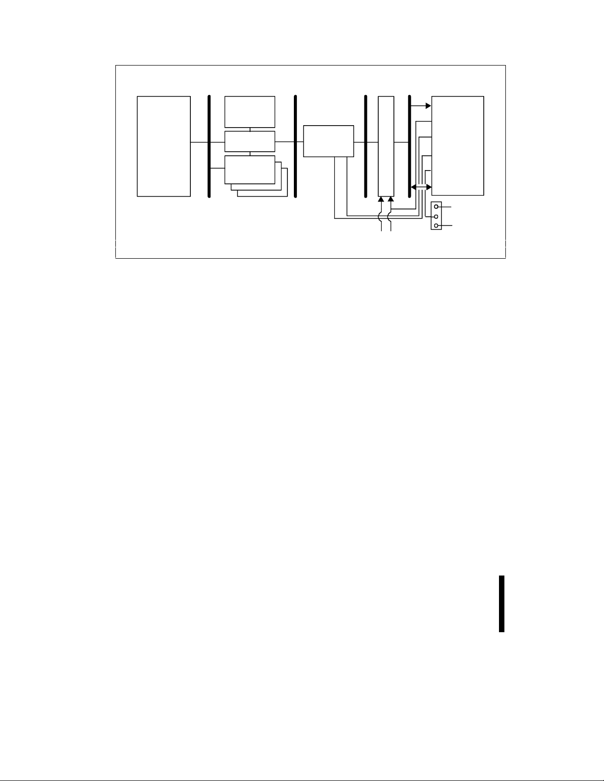
handwriting, and diagnostic code. Figure 1 shows
an example 28F002BC application.
The 28F002BC is also an excellent design soluti on
for analog and digital cellular phone and
telecommunication switching applications requiring
high-performance, high-density storage in a small
form factor package (x8-only bus). The blocking
structure allows for easy segmentation of
embedded code for modular software designs . For
example, the parameter block can be used for
frequently updated data storage and diagnostic
messages (e.g., phone numbers and authorization
codes).
The increase in software sophistication augments
the probability that a code update will be required
after the PC is shipped. The 28F002BC provides a
1.4 Pinouts
safe and inexpensive update solution for desktop,
notebook, and hand-held personal computers while
extending the product lifetime. Furthermore, the
deep power-down mode provides added flexibility
for those battery-operated portable designs that
require low power.
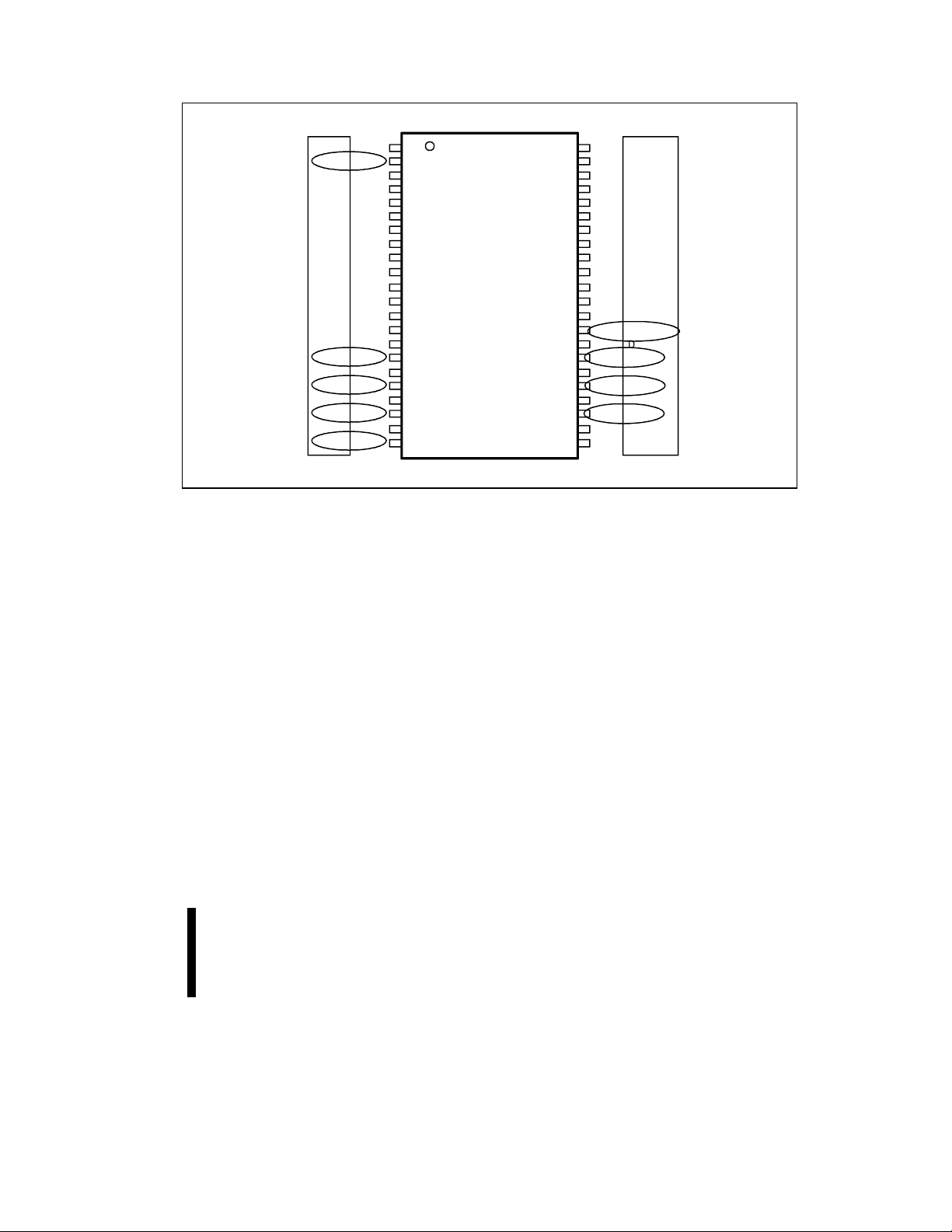
The 28F002BC in the 44-lead PSOP pinout f ollows
the industry-standard ROM/EPROM pinout, as
shown in Figure 4. The 2-Mbit SmartVoltage pi nout,
indicating the WP# input, is al so shown in the s ame
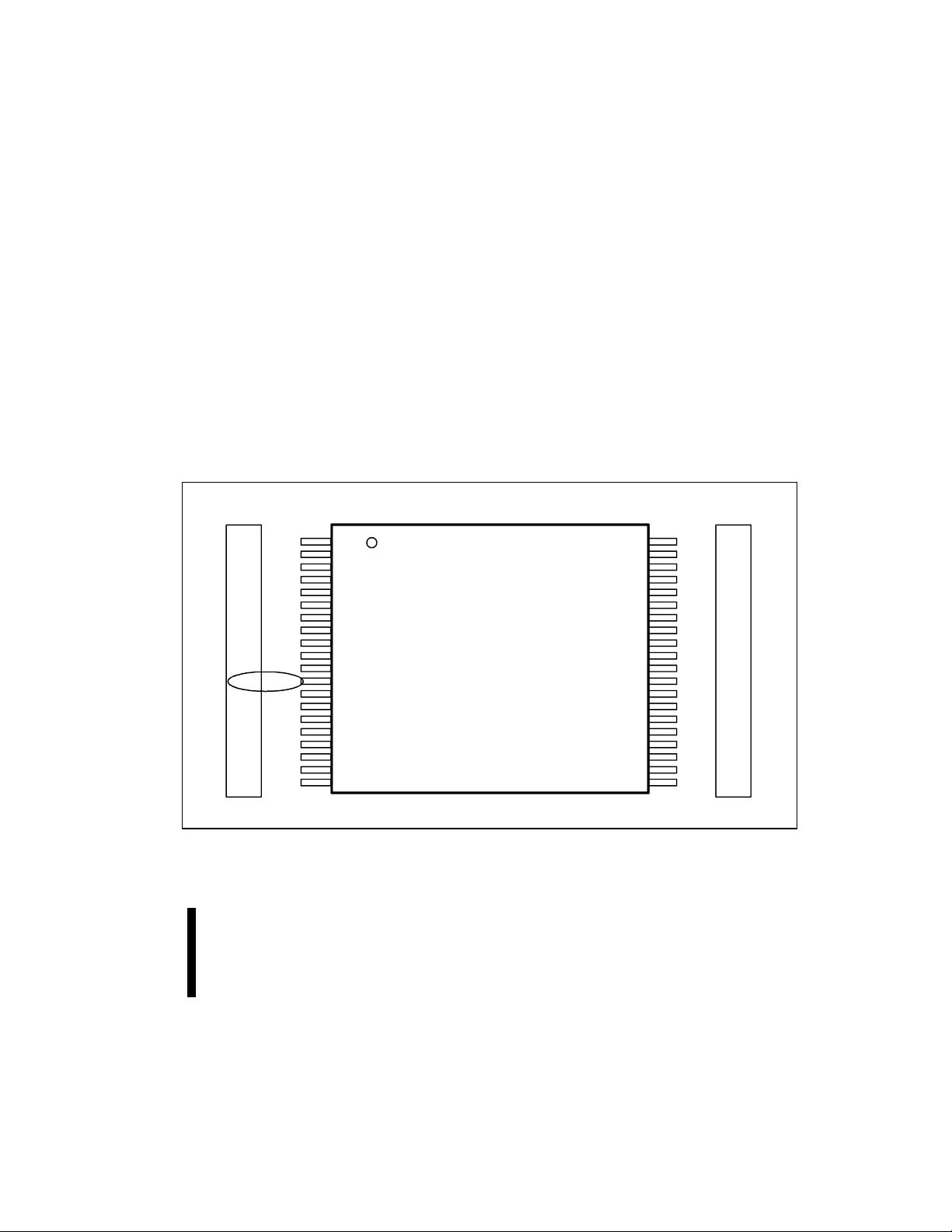
diagram. The 40-lead TSOP package (shown in
Figure 2) offers the smalles t form fac tor possible in
addition to being compatible with i ts SmartVoltage
upgrade in the same package. The l ow-cost 40-lead
PDIP package diagram is shown in Figure 3.
28F002BV 28F002BV
A
A
16
A
A
A
A
A
WE#
RP#
V
WP#
NC
A
A
A
A
A
A
A
16
A
15
15
A
14
14
A
13
13
A
12
12
A
11
11
A
A
9
A
PP
9
A
8
8
WE#
RP#
V
PP
NC
NC
A
7
7
A
6
6
A
5
5
A
4
4
A
3
3
A
2
2
A
1
1
1
2
3
4
5
6
7
8
9
10
11
12
13
14
15
16
17
18
19
20
E28F002BC
BOOT BLOCK
40-LEAD TSOP
10 mm x 20 mm
TOP VIEW
40
39
38
37
36
35
34
33
32
31
30
29
28
27
26
25
24
23
22
21
A
17
GND
NC
NC
A
10
DQ
DQ
DQ
DQ
V
CC
V
CC
NC
DQ
DQ
DQ
DQ
OE#
GND
CE#
A
0
A
17
GND
NC
NC
A
10
DQ
7
7
DQ
6
6
DQ
5
5
DQ
4
4
V
CC
V
CC
NC
DQ
3
3
DQ
2
2
DQ
1
1
DQ
0
0
OE#
GND
CE#
A
0
0578_02
Figure 2. The 40-Lead TSOP Offers the Smallest Form Factor for Space-Constrained Applications
PRELIMINARY
7

28F002BC 2-MBIT BOOT BLOCK FLASH MEMORY E
NC
NC
A
CE#
GND
OE#
DQ
DQ
DQ
DQ
V
V
DQ
DQ
DQ
DQ
A
GND
A
NC
CC
CC
1
2
3
0
4
5
P28F002BC
BOOT BLOCK
6
40-LEAD PDIP
7
0
8
1
9
2
10
3
11
12
13
4
14
5
15
6
16
7
17
10
18
19
17
20
40
NC
A
39
A
38
A
37
A
36
A
35
A
34
A
33
V
32
31
RP#
30
WE#
A
29
A
28
A
27
A
26
A
25
A
24
A
23
A
22
21 NC
1
2
3
4
5
6
7
PP
8
9
11
12
13
14
15
16
0578_3A
Figure 3. The 40-Lead PDIP Offers the Lowest Cost Package Solution
8
PRELIMINARY

E 28F002BC 2-MBIT BOOT BLOCK FLASH MEMORY
28F200BV
V
PP
WP#
NC
A
7
A
6
A
5
A
4
A
3
A
2
A
1
A
0
CE#
GND
OE#
DQ
0
DQ
8
DQ
1
DQ
9
DQ
2
DQ
10
DQ
3
DQ
11
V
PP
NC
NC
A
7
A
6
A
5
A
4
A
3
A
2
A
1
A
0
CE#
GND
OE#
DQ
NC
DQ
NC
DQ
NC
DQ
NC
1
2
3
4
5
6
7
8
9
10
PA28F002BC
BOOT BLOCK
44-Lead PSOP
0.525" x 1.110"
11
12
13
TOP VIEW
14
15
0
16
1
18
19
2
20
21
3
22
44
43
42
41
40
39
38
37
36
35
34
33
32
31
30
29
2817
27
26
25
24
23
28F200BV
RP#
RP#
WE#
WE#
A
A
8
A
A
9
A
A
10
A
A
11
A
A
12
A
A
13
A
A
14
A
A
15
A
A
16
NC NC
GND
GND
A
DQ15/A
-1
DQ
DQ
7
DQ
NC
DQ
DQ
6
DQ
NC
DQ
DQ
5
DQ
NC
DQ
DQ
4
V
CCVCC
8
9
10
11
12
13
14
15
16
-1
7
14
6
13
5
12
4
Figure 4. The 44-Lead PSOP Offers a Convenient Upgrade from JEDEC ROM Standards
0578_03
PRELIMINARY
9

28F002BC 2-MBIT BOOT BLOCK FLASH MEMORY E
1.5 Pin Descriptions
Table 1. 28F002BC Pin Descriptions
Symbol Type Name and Function
A–1,
A
–A
0
A
9
DQ0–
DQ
7
INPUT
17
INPUT ADDRESS INPUT: When A9 is at V
INPUT/
OUTPUT
CE# INPUT CHIP ENABLE: Activates the device’s control logic, input buffers, decoders and
OE# INPUT OUTPUT ENABLE: Enables the device’s outputs through the data buffers
WE# INPUT WRITE ENABLE: Controls writes to the Command Register and array blocks.
RP# INPUT RESET/DEEP POWER-DOWN: Provides three-state control. Puts the device in
V
CC
V
PP
GND GROUND: For all internal circuitry.
NC NO CONNECT: Pin may be driven or left floating.
ADDRESS INPUTS for memory addresses. Addresses are internally latched
during a write cycle. A
is used on the PSOP package only. A
-1
is used on the
17
TSOP and PDIP packages.
the signature mode is accessed. During
this mode, A
decodes between the manufacturer and device IDs.
0
HH,
DATA INPUTS/OUTPUTS: Inputs array data on the second CE# and WE#
cycle during a program operation. Inputs commands to the Command User
Interface when CE# and WE# are active. Data is internally latched during the
write cycle. Outputs array, Intelligent Identifier and Status register data. The
data pins float to tri-state when the chip is de-selected or the outputs are
disabled.
sense amplifiers. CE# is active low. CE# high deselects the memory device and
reduces power consumption to standby levels. If CE# and RP# are high, but not
at a CMOS high level, the standby current will increase due to current flow
through the CE# and RP# input stages.
during a read cycle. OE# is active low.
WE# is active low. Addresses and data are latched on the rising edge of the
WE# pulse.
deep power-down mode, locks, and unlocks the boot block from program/erase.
When RP# is at logic high level (6.5V maximum), the boot block is locked and
cannot be programmed or erased.
When RP# = V
programmed or erased.
(11.4V minimum ), the boot block is unlocked and can be
HH
When RP# is at a logic low level the boot block is locked, the deep power-down
mode is enabled and the WSM is reset—preventing any blocks from being
programmed or erased. When RP# transitions from logic low to logic high, the
flash memory enters the read array mode.
DEVICE POWER SUPPLY: 5.0V ± 10%, 5.0V ± 5%
PROGRAM/ERASE POWER SUPPLY: For erasing memory array blocks or
programming data in each block. When V
memory contents cannot be altered.
PP
< V
all blocks are locked and
PPLK
10
PRELIMINARY

E 28F002BC 2-MBIT BOOT BLOCK FLASH MEMORY
2.0 PRODUCT DESCRIPTION
DQ -DQ
07
A -A
0
Output
Buffer
Identifier
Register
Output
Power
Reduction
Control
17
Input
Buffer
Address
Latch
Address
Counter
Y-Decoder
X-Decoder
16-Kbyte
Boot Block
Multiplexer
8-Kbyte
Parameter Block
Status
Register
Data
Comparator
Y-Gating/Sensing
8-Kbyte
Parameter Block
Input
Buffer
I/O Logic
Data
Register
96-Kbyte
Main Block
128-Kbyte
Main Block
Command
User
Interface
Write State
Machine
Program/Erase
Voltage Switch
CE#
WE#
OE#
RP#
V
PP
V
GND
044819
CC
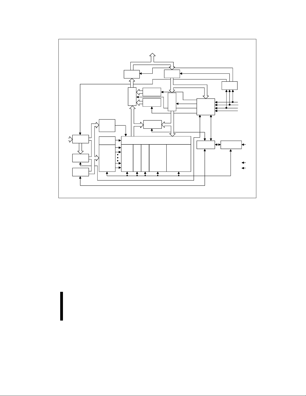
Figure 5. 28F002BC Internal Block Diagram
PRELIMINARY
11

28F002BC 2-MBIT BOOT BLOCK FLASH MEMORY E
2.1 Memory Organization
2.1.1 BLOCKING
The 28F002BC features an asymmetric ally-blocked
architecture that provides system memory
integration. Each block can be erased up to
100,000 times. The block sizes have been chosen
to optimize their functionality for common
applications of nonvolat ile storage. For t he address
locations of the blocks, see the memory map in
Figure 6.
2.1.1.1 Boot Block - 16 KB
The boot block is intended to repl ace a dedicated
boot PROM in a microprocess or or microcontrollerbased system. The 16-Kbyte (16,384 bytes) boot
block is located at t he top of the address map as
shown in Figure 6. This boot block features
hardware controllable write-protection to protec t the
crucial microprocessor boot code from accidental
erasure. The boot block can be erased and written
when RP# is held at 12V for the duration of the
erase or program operation. This feature allows
customers to change the boot code when
necessary while providing security at other times.
28F002BC-T
3FFFFH
3C000H
3BFFFH
3A000H
39FFFH
38000H
37FFFH
20000H
1FFFFH
00000H
Figure 6. 28F002BC-T Memory Map
16-Kbyte Boot Block
8-Kbyte Parameter Block
8-Kbyte Parameter Block
96-Kbyte Main Block
128-Kbyte Main Block
0578_05
2.1.1.2 Parameter Blocks - 8 KB (each)
The 28F002BC has two 8-Kbyte parameter blocks
to facilitate storage of frequently updated system
parameters that would normally require an
EEPROM. The parameter blocks can also be used
to store additional boot or main code. By using
software techniques, the byte-rewrite functionality
of EEPROMs can be emulated. These t echniques
are detailed in Intel’s appli cat ion note
AP-604 Using
Intel’s Boot Bloc k Flash Memory Parameter Block s
to Replace EEPROM.
2.1.1.3 Main Block - 96 KB and 128 KB
The 28F002BC contains one 96-Kbyte (98,304
byte) block and one 128-Kbyte (131,072 byte)
block. These blocks are typically used for data or
code storage.
2.1.2 28F002BC-T BLOCK MEMORY MAP
The 16-Kbyte boot block of the 28F002BC-T is
located from 3C000H to 3FFFFH. The first 8-Kbyte
parameter block resides in memory space from
3A000H to 3BFFFH. The second 8-Kbyte
parameter block consumes the memory area from
38000H to 39FFFH. The 96-Kbyte main block
extends from 20000H to 37FFFH, while the
128-Kbyte main block occupies the region from
00000H to 1FFFFH.
3.0 PRINCIPLES OF OPERATION
Flash memory improves upon EPROM capability
with in-circuit electrical write and erase. The Boot
Block flash memory utilizes a Command User
Interface (CUI) and automated algorithms to
simplify write and erase operations. The CUI allows
for 100% TTL-level control inputs, fixed power
supplies during erasure and programming, and
maximum EPROM compatibility.
When V
execute the following commands: Read Array,
Read Status register, Clear Status register, and
Intelligent Identifier. The device provides standard
EPROM read, standby and output disable
operations. Manufacturer identification and device
identification data c an be acc ess ed through t he CUI
or through the standard EPROM A
(V
High voltage on V
device. With V
< V
PP
) access for PROM programming equipment.
ID
, the device will only successfully
PPLK
high voltage
9
allows write and erase of the
PP
active, all functions associated
PP
12
PRELIMINARY
 Loading...