Intel Corporation G28F640J5-150, G28F320J5-120, E28F320J5-120, DA28F640J5-150, DA28F320J5-120 Datasheet

E
January 1998
INTEL StrataFlash™ MEMORY TECHNOLOGY
n
High-Density Symmetrically-Blocked
Architecture
64 128-Kbyte Erase Blocks (64 M)
32 128-Kbyte Erase Blocks (32 M)
n
5 V VCC Operation
2.7 V I/O Capable
n
Configurable x8 or x16 I/O
n
120 ns Read Access Time (32 M)
150 ns Read Access Time (64 M)
n
Enhanced Data Protection Features
Absolute Protection with
Flexible Block Locking
Block Erase/Program Lockout
n
Industry-Standard Packaging
µBGA* Package, SSOP and TSOP
= GND
V
PEN
during Power Transitions
Packages (32 M)
32 AND 64 MBIT
28F320J5 and 28F640J5
n
Cross-Compatible Command Support
Intel Basic Command Set
Common Flash Interface
Scaleable Command Set
n
32-Byte Write Buffer
6 µs per Byte Effective
Programming Time
n
640,000 Total Erase Cycles (64 M)
320,000 Total Erase Cycles (32 M)
10,000 Erase Cycles per Block
n
Automation Suspend Options
Block Erase Suspend to Read
Block Erase Suspend to Program
n
System Performance Enhancements
STS Status Output
n
Intel StrataFlash™ Memory Flash
Technology
ADVANCE INFORMATION
Capitalizing on two-bit-per-cell tec hnology, Int el Strat aFlash™ m emory produc ts provide 2X the bit s in 1X the
space. Offered in 64-Mbit (8-Mbyte) and 32-Mbit (4-Mbyte) densities, Intel StrataFlash mem ory devices are
the first to bring reliable, two-bit-per-cell storage technology to the flash market.
Intel StrataFlash memory benefits include: more density in less space, lowest cost-per-bit NOR devices,
support for code and data storage, and easy migration to future devices.
Using the same NOR-based ETOX™ technology as Intel’s one-bit-per-cell products, Intel StrataFlash
memory
Intel StrataFlash c omponents are ideal for code or data applications where high density and l ow cost are
required. Examples include networking, telecommunications, audio recording, and digital imaging.
By applying FlashFile™ mem ory family pinouts, Intel StrataFlash m emory components allow easy design
migrations from existi ng 28F016SA/SV, 28F032SA, and Word-W ide FlashFile memory devices (28F160S5
and 28F320S5).
Intel StrataFlash mem ory components deliver a new generation of forward-compatible software support . By
using the Common Flash Interface (CFI) and the Scaleable Command Set (SCS), customers can take
advantage of density upgrades and optimized write capabilities of future Intel StrataFlash memory devices.
Manufactured on Intel’s 0.4 m icron ETOX™ V process technology, I ntel StrataFlash memory provides the
highest levels of quality and reliability.
devices take advantage of 400 million units of manufacturing experience since 1988. As a result,
Order Number: 290606-004

Information in this document is provided in connection with Intel products. No license, express or implied, by estoppel or
otherwise, to any intellectual property rights is granted by this document. Except as provided in Intel’s Terms and Conditions of
Sale for such products, Intel assumes no liability whatsoever, and Intel disclaims any express or implied warranty, relating to
sale and/or use of Intel products including liability or warranties relating to fitness for a particular purpose, merchantability, or
infringement of any patent, copyright or other intellectual property right. Intel products are not intended for use in medical, life
saving, or life sustaining applications.
Intel may make changes to specifications and product descriptions at any time, without notice.
The 28F320J5 and 28F640J4 may contain design defects or errors known as errata. Current characterized errata are available
on request.
Contact your local Intel sales office or your distributor to obtain the latest specifications and before placing your product order.
Copies of documents which have an ordering number and are referenced in this document, or other Intel literature, may be
obtained from:
Intel Corporation
P.O. Box 5937
Denver, CO 80217-9808
or call 1-800-548-4725
or visit Intel’s website at http://www.intel.com
COPYRIGHT © INTEL CORPORATION 1997, 1998 CG-041493
*Third-party brands and names are the property of their respective owners.
2

E INTEL StrataFlash™ MEMORY TECHNOLOGY, 32 AND 64 MBIT
CONTENTS
PAGE PAGE
1.0 PRODUCT OVERVIEW...................................5
2.0 PRINCIPLES OF OPERATION .....................11
2.1 Data Protection ..........................................12
3.0 BUS OPERATION.........................................12
3.1 Read..........................................................13
3.2 Output Disable...........................................13
3.3 Standby......................................................13
3.4 Reset/Power-Down....................................13
3.5 Read Query................................................14
3.6 Read Identifier Codes.................................14
3.7 Write ..........................................................14
4.0 COMMAND DEFINITIONS............................14
4.1 Read Array Command................................18
4.2 Read Query Mode Command.....................18
4.2.1 Query Structure Output .......................18
4.2.2 Query Structure Overview ...................20
4.2.3 Block Status Register..........................21
4.2.4 CFI Query Identification String.............22
4.2.5 System Interface Information...............23
4.2.6 Device Geometry Definition.................24
4.2.7 Primary-Vendor Specific Extended
Query Table .......................................25
4.3 Read Identifier Codes Command...............26
4.4 Read Status Register Command................27
4.5 Clear Status Register Command................27
4.6 Block Erase Command ..............................27
4.7 Block Erase Suspend Command................27
4.8 Write to Buffer Command...........................28
4.9 Byte/Word Program Commands.................28
4.10 Configuration Command...........................29
4.11 Set Block and Master Lock-Bit
Commands................................................29
4.12 Clear Block Lock-Bits Command..............30
5.0 DESIGN CONSIDERATIONS........................40
5.1 Three-Line Output Control..........................40
5.2 STS and Block Erase, Program, and Lock-
Bit Configuration Polling............................40
5.3 Power Supply Decoupling ..........................40
, V
5.4 V
CC
5.5 Power-Up/Down Protection........................41
5.6 Power Dissipation.......................................41
6.0 ELECTRICAL SPECIFICATIONS..................42
6.1 Absolute Maximum Ratings........................42
6.2 Operating Conditions..................................42
6.3 Capacitance...............................................42
6.4 DC Characteristics .....................................43
6.5 AC Characteristics— Read-Only
Operations.................................................45
6.6 AC Characteristics— Write Operations.......48
6.7 Block Erase, Program, and Lock-Bit
Configuration Performance........................51
7.0 ORDERING INFORMATION.........................52
8.0 ADDITIONAL INFORMATION......................53
, RP# Transitions........................40
PEN
ADVANCE INFORMATION
3

INTEL StrataFlash™ MEMORY TECHNOLOGY, 32 AND 64 MBIT E
CCE
FIGURES
Figure 1. Intel StrataFlash™ Memory Block
Diagram.............................................. 6
Figure 2. µBGA* Package (64-Mbit and 32-Mbit)9
Figure 3. TSOP Lead Configuration (32-Mbit)..10
Figure 4. SSOP Lead Configuration (64-Mbit
and 32-Mbit).....................................11
Figure 5. Memory Map.....................................12
Figure 6. Device Identifier Code Memory Map .14
Figure 7. Write to Buffer Flowchart...................34
Figure 8. Byte/Word Program Flowchart ..........35
Figure 9. Block Erase Flowchart ......................36
Figure 10. Block Erase Suspend/Resume
Flowchart..........................................37
Figure 11. Set Block Lock-Bit Flowchart...........38
Figure 12. Clear Block Lock-Bit Flowchart........39
Figure 13. Transient Input/Output Reference
Waveform for V
= 5.0 V ± 10%
CCQ
(Standard Testing Configuration)......45
Figure 14. Transient Input/Output Reference
Waveform for V
= 2.7 V−3.6V.....45
CCQ
Figure 15. Transient Equivalent Testing Load
Circuit...............................................45
Figure 16. AC Waveform for Read Operations.47
Figure 17. AC Waveform for Write Operations.49
Figure 18. AC Waveform for Reset Operation..50
TABLES
Table 1. Lead Descriptions.................................7
Table 2. Chip Enable Truth Table.....................13
Table 3. Bus Operations...................................15
Table 4. Intel StrataFlash™ Memory Command
Set Definitions ...................................16
Table 5. Summary of Query Structure Output as
a Function of Device and Mode .........19
Table 6. Example of Query Structure Output of
a x16- and x8-Capable Device...........19
Table 7. Query Structure..................................20
Table 8. Block Status Register.........................21
Table 9. CFI Identification ................................22
Table 10. System Interface Information............23
Table 11. Device Geometry Definition..............24
Table 12. Primary Vendor-Specific Extended
Query.................................................25
Table 13. Identifier Codes ................................26
Table 14. Write Protection Alternatives ............30
Table 15. Configuration Coding Definitions.......31
Table 16. Status Register Definitions ...............32
Table 17. eXtended Status Register Definitions33
REVISION HISTORY
Date of
Revision
09/01/97 -001 Original Version
09/17/97 -002 Modifications made to cover sheet
12/01/97 -003 VCC/GND Pins Converted to No Connects specification change added
1/31/98 -004 The µBGA* chip-scale package in Figure 2 was changed to a 52-ball
4
Version Description
I
, I
, I
CCS
CCD
CCW
, and I
specification change added
Order Codes specification change added
package and appropriate documentation added. The 64-Mb µBGA
package dimensions were changed in Figure 2. Changed Figure 4 to
read SSOP instead of TSOP.
ADVANCE INFORMATION

E INTEL StrataFlash™ MEMORY TECHNOLOGY, 32 AND 64 MBIT
1.0 PRODUCT OVERVIEW
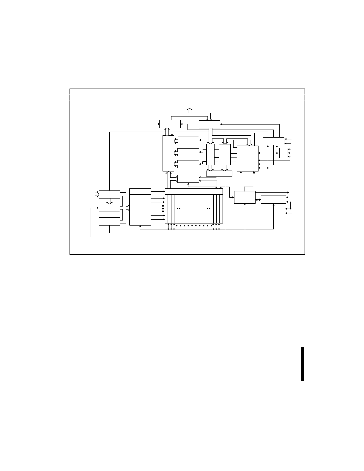
The Intel StrataFlash™ memory family contains
high-density memories organiz ed as 8 Mbytes or
4 Mwords (64-Mbit) and 4 Mbytes or 2 Mwords
(32-Mbit). These devices c an be accessed as 8- or
16-bit words. The 64-Mbit devic e is organized as
sixty-four 128-Kbyt e (131,072 bytes) erase block s
while the 32-Mbits devic e contains thirty-two 128Kbyte erase blocks. Blocks are selectively and
individually lockable and unlockable in-system.
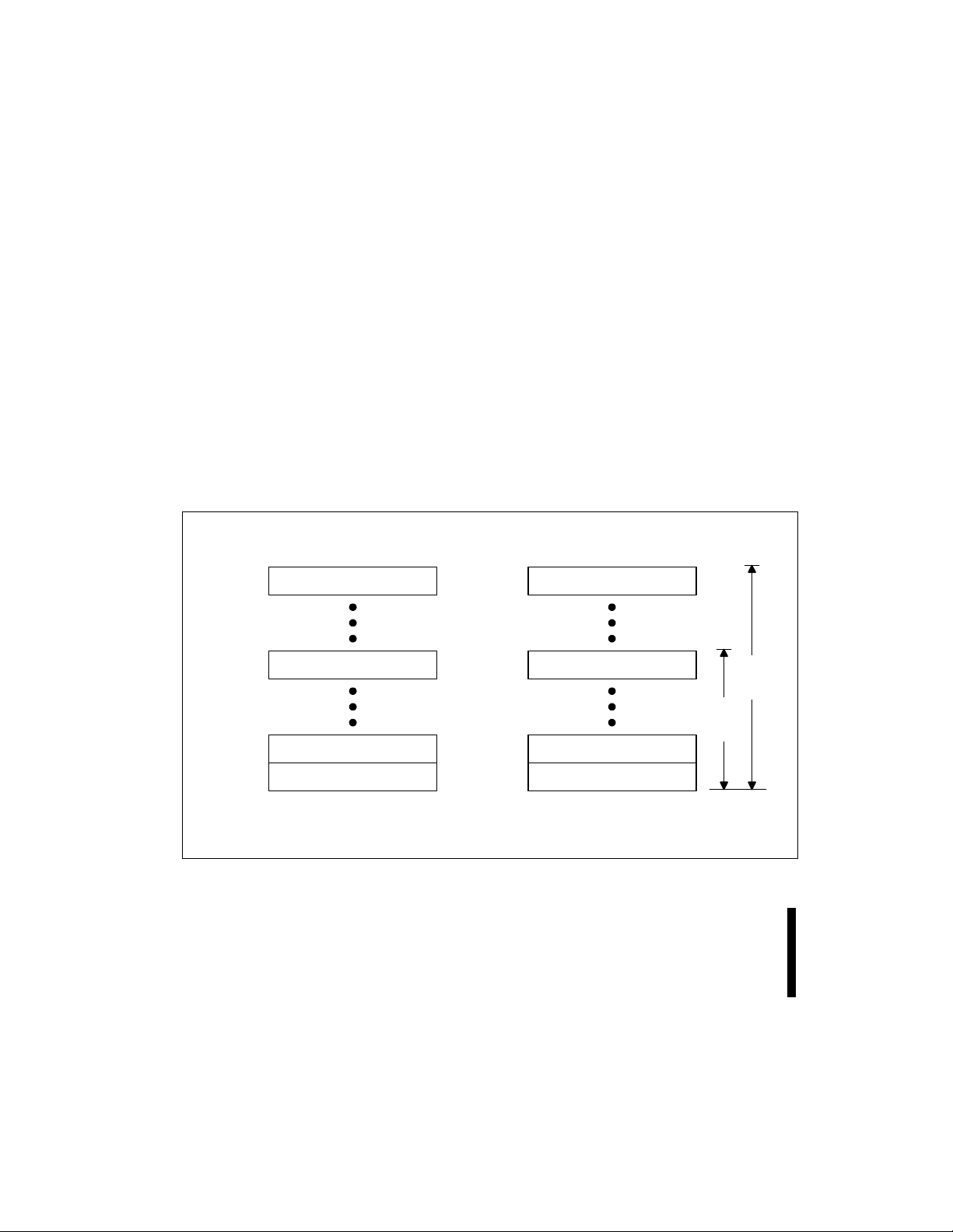
See the memory map in Figure 5.
A Common Flash Interface (CFI) permit s software
algorithms to be used for entire families of
devices. This allows device-independent, JEDEC
ID-independent, and forward- and backwardcompatible software support for the s pecified f lash
device families. Flash vendors can standardize
their existing interfaces for long-term compatibility.
Scaleable Command Set (SCS) allows a single,
simple software driver in all host systems to work
with all SCS-compliant flash memory devices,
independent of system-level packaging (e.g.,
memory card, SIMM, or direct-to-board placement). Additionally, SCS provides the highest
system/device data transfer rates and minimizes
device and system-level implementation costs.
A Command User Interface (CUI) serves as the
interface between the system processor and
internal operation of the device. A vali d command
sequence written to the CUI initiates device
automation. An internal Write State Machine
(WSM) automatically executes the algorithms and
timings necessary for block erase, program, and
lock-bit configuration operations.
Individual block locki ng uses a com binati on of bit s,
block lock-bits and a m aster lock-bit, to lock and
unlock blocks. Block lock-bits gate block erase
and program operations while the mast er lock-bit
gates block lock-bit modification. Three lock-bit
configuration operations set and clear lock-bits
(Set Block Lock-Bit, Set Master Lock-Bit, and
Clear Block Lock-Bits commands).
The status register indicates when the WSM’s
block erase, program, or lock-bit configuration
operation is finished.
The STS (STATUS) output gives an additional
indicator of WSM activity by providing both a
hardware signal of status (vers us soft ware polling)
and status masking (interrupt masking for
background block erase, for example). Status
indication using STS minimizes both CPU
overhead and system power consumption. When
configured in level mode (default mode), it acts as
a RY/BY# pin. When low, STS indic ates that the
WSM is performing a block erase, program, or
lock-bit configuration. S TS-high indicates that the
WSM is ready for a new command, block erase is
suspended (and programming is inactive), or the
device is in reset/power-down m ode. Additionally,
the configuration command al lows the STS pin to
be configured to pulse on completion of
programming and/or block erases.
Three CE pins are used to enable and disable the
device. A unique CE logic design (see Table 2,
Chip Enable Truth Table
typically required for multi-chip designs. External
logic is not required when designing a s ingle chip,
a dual chip, or a 4-chip miniature card or SIMM
module.
) reduces decoder logic
A block erase operation erases one of the devic e’s
128-Kbyte blocks typically within one second—
independent of other blocks. Each block can be
independently erased 10,000 times. Block erase
suspend mode allows system software to suspend
block erase to read or program data from any
other block.
Each device incorporates a Write Buffer of
32 bytes (16 words) to allow optimum
programming performance. By using the Write
Buffer, data is programmed in buffer increments.
This feature can improve system program
performance by up to 20 times over non Write
Buffer writes.
ADVANCE INFORMATION
The BYTE# pin allows either x8 or x16 read/writes
to the device. BYTE# at logic low selects 8-bit
mode; address A
and high byte. BYTE# at logic high enables 16-bit
operation; address A
address and address A
device block diagram is shown in Figure 1.
When the device is disabled (see Table 2,
Enable Truth Table
standby mode is enabled. When the RP # pin is at
GND, a further power-down mode is enabled
which minimizes power consumpti on and provides
write protection during reset. A reset time (t
is required from RP# switc hing high until outputs
selects between the low byte
0
becomes the lowest order
1
is not used (don’t care). A
0
) and the RP# pin is at VCC, the
Chip
PHQV
)
5
INTEL StrataFlash™ MEMORY TECHNOLOGY, 32 AND 64 MBIT E
are valid. Likewise, the device has a wake time
(t
) from RP#-high until writes t o the CUI are
PHWL
recognized. With RP# at GND, the WSM is reset
and the status register is cleared.
The Intel StrataFlash memory devices are
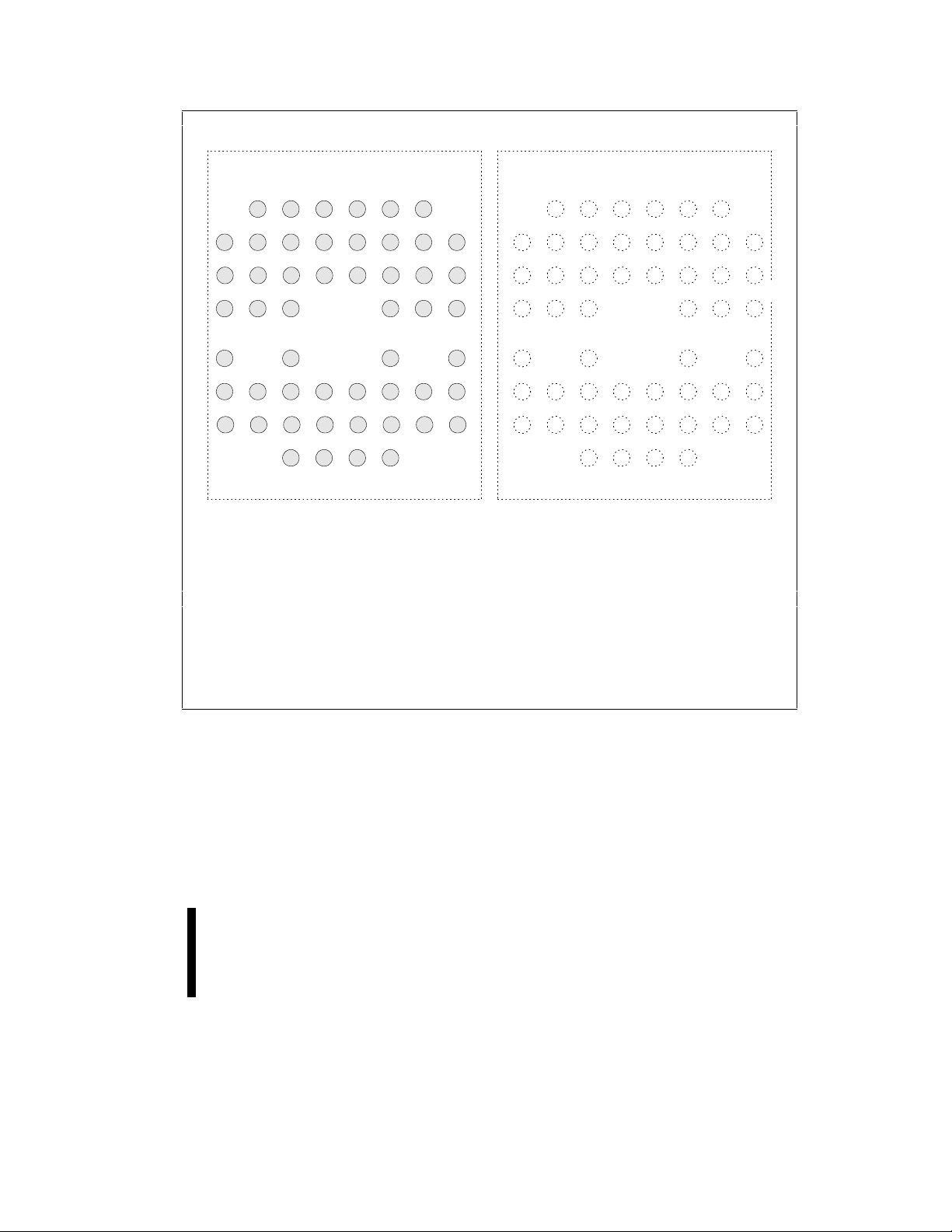
available in several pack age types. The 64-Mbit i s
V
32-Mbit: A0- A
64-Mbit: A
0 - A22
CCQ
21
Input Buffer
Address
Latch
Address
Counter
Y-Decoder
X-Decoder
Output Buffer
Output
Multiplexer
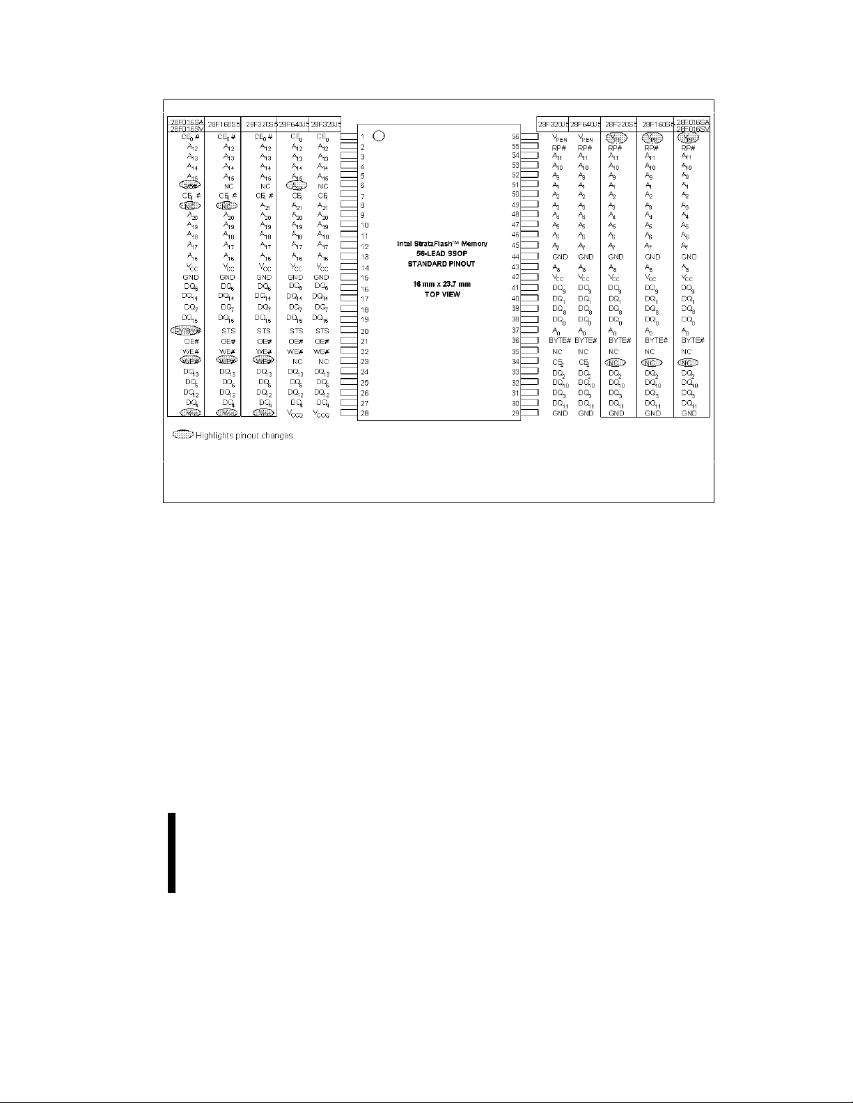
available in 56-lead SSOP (Shrink Small Outline
Package) and µBGA* package (micro Ball Grid
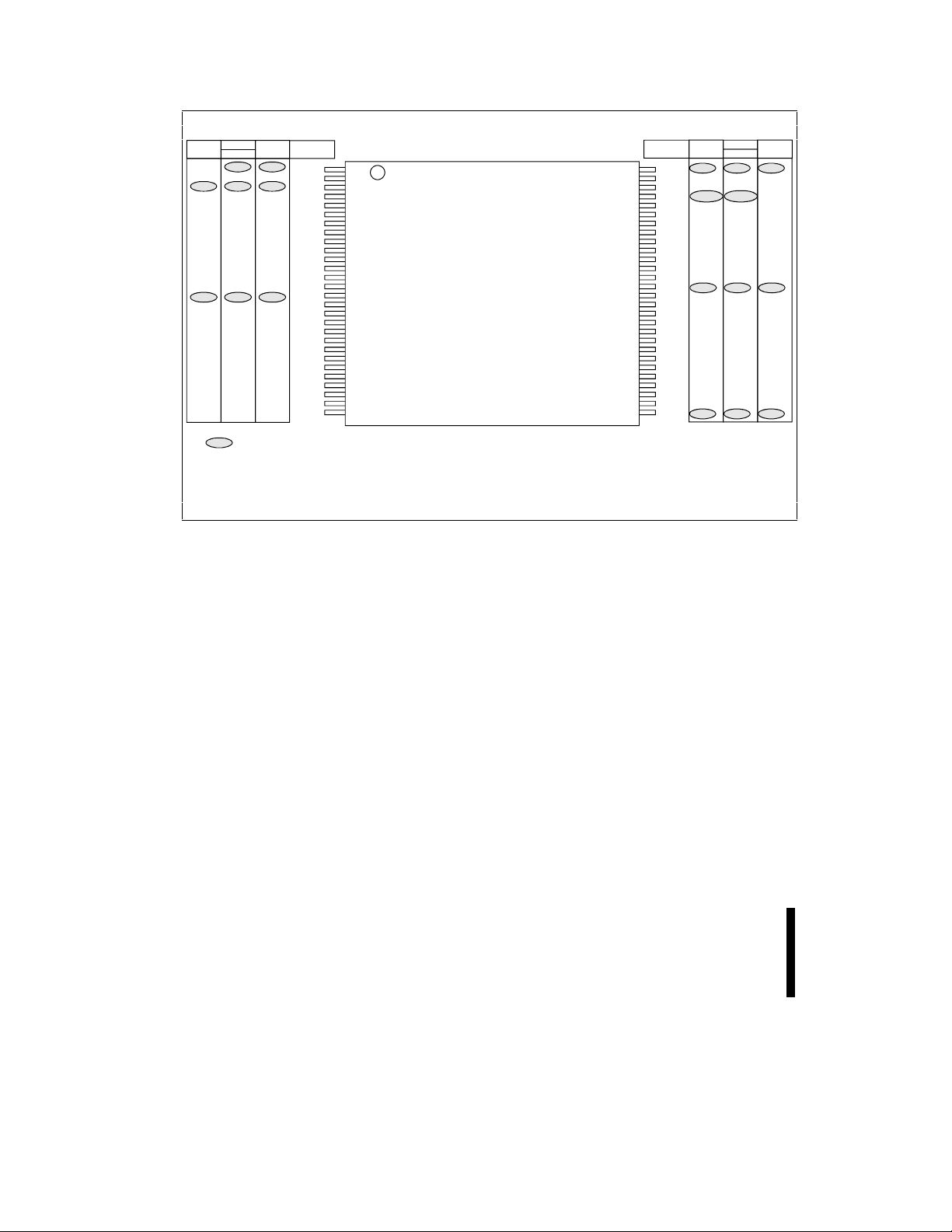
Array). The 32-Mbit is availabl e in 56-lead TSOP
(Thin Small Outline Pack age), 56-lead SSOP, and
56-bump µBGA packages. Figures 2, 3, and 4
show the pinouts.
DQ0 - DQ
15
Input Buffer
Query
Identifier
Register
Status
Register
Data
Comparator
Y-Gating
32-Mbit: Thirty-two
64-Mbit: Sixty-four
128-Kbyte Blocks
Data
Register
Multiplexer
Command
Write Buffer
User
Interface
Write State
Machine
I/O Logic
Program/Erase
Voltage Switch
CE
Logic
WE#
STS
V
CC
BYTE#
CE
CE
CE
OE#
RP#
V
PEN
V
CC
GND
0
1
2
0606_01
Figure 1. Intel StrataFlash™ Memory Block Diagram
6
ADVANCE INFORMATION

E INTEL StrataFlash™ MEMORY TECHNOLOGY, 32 AND 64 MBIT
Table 1. Lead Descriptions
Symbol Type Name and Function
A
0
A1–A
22
DQ0–DQ
DQ8–DQ
CE0,
CE
,
1
CE
2
RP# INPUT RESET/ POWER-DOWN: Resets internal automation and puts the device in
OE# INPUT OUTPUT ENABLE: Activates the device’s outputs through the data buffers
WE# INPUT WRITE ENABLE: Controls writes to the Command User Interface, the Write
STS OPEN
INPUT BYTE-SELECT ADDRESS: Selects between high and low byte when the device
INPUT ADDRESS INPUTS: Inputs for addresses during read and program operations.
INPUT/
7
OUTPUT
INPUT/
15
OUTPUT
INPUT CHIP ENABLES: Activates the device’s control logic, input buffers, decoders,
DRAIN
OUTPUT
is in x8 mode. This address is latched during a x8 program cycle. Not used in
x16 mode (i.e., the A
Addresses are internally latched during a program cycle.
32-Mbit: A
64-Mbit: A0–A
LOW-BYTE DATA BUS: Inputs data during buffer writes and programming, and
inputs commands during Command User Interface (CUI) writes. Outputs array,
query, identifier, or status data in the appropriate read mode. Floated when the
chip is de-selected or the outputs are disabled. Outputs DQ
floated when the Write State Machine (WSM) is busy. Check SR.7 (Status
Register bit 7) to determine WSM status.
HIGH-BYTE DATA BUS: Inputs data during x16 buffer writes and programming
operations. Outputs array, query, or identifier data in the appropriate read mode;
not used for Status Register reads. Floated when the chip is de-selected, the
outputs are disabled, or the WSM is busy.
and sense amplifiers. When the device is de-selected (see Table 2,
Truth Table
All timing specifications are the same for these three signals. Device selection
occurs with the first edge of CE
deselection occurs with the first edge of CE
device (see Table 2,
power-down mode. RP#-high enables normal operation. Exit from reset sets the
device to read array mode. When driven low, RP# inhibits write operations which
provides data protection during power transitions.
RP# at V
when the master lock-bit is set. RP# = V
enabling block erase and programming operations to locked memory blocks. Do
not permanently connect RP# to V
during a read cycle. OE# is active low.
Buffer, and array blocks. WE# is active low. Addresses and data are latched on
the rising edge of the WE# pulse.
STATUS: Indicates the status of the internal state machine. When configured in
level mode (default mode), it acts as a RY/BY# pin. When configured in one of
its pulse modes, it can pulse to indicate program and/or erase completion. For
alternate configurations of the STATUS pin, see the Configurations command.
Tie STS to V
0–A21
), power reduces to standby levels.
enables master lock-bit setting and block lock-bits configuration
HH
CCQ
input buffer is turned off when BYTE# is high).
0
22
, CE1, or CE2 that enables the device. Device
0
Chip Enable Truth Table
HH
with a pull-up resistor.
, CE1, or CE2 that disables the
0
).
overrides block lock-bits thereby
HH
.
–DQ0 are also
6
Chip Enable
ADVANCE INFORMATION
7

INTEL StrataFlash™ MEMORY TECHNOLOGY, 32 AND 64 MBIT E
Table 1. Lead Descriptions (Continued)
Symbol Type Name and Function
BYTE# INPUT BYTE ENABLE: BYTE# low places the device in x8 mode. All data is then input
V
PEN
V
CC
V
CCQ
INPUT ERASE / PROGRAM / BLOCK LOCK ENABLE: For erasing array blocks,
SUPPLY DEVICE POWER SUPPLY: With VCC ≤ V
OUTPUT
BUFFER
SUPPLY
GND SUPPLY GROUND: Do not float any ground pins.
NC NO CONNECT: Lead is not internally connected; it may be driven or floated.
or output on DQ
–DQ7, while DQ8–DQ15 float. Address A0 selects between the
0
high and low byte. BYTE# high places the device in x16 mode, and turns off the
A
input buffer. Address A1 then becomes the lowest order address.
0
programming data, or configuring lock-bits.
With V
PEN
≤ V
, memory contents cannot be altered.
PENLK
LKO
, all write attempts to the flash
memory are inhibited.
OUTPUT BUFFER POWER SUPPLY: This voltage controls the device’s output
voltages. To obtain output voltages compatible with system data bus voltages,
connect V
to the system supply voltage.
CCQ
8
ADVANCE INFORMATION
E INTEL StrataFlash™ MEMORY TECHNOLOGY, 32 AND 64 MBIT
78 6543
21
21 3456
78
A
GND A10V
PENCE0A14VCC
V
14
CC
PEN
0
V
CE
A
GNDA
10
B
A7A9A11A12A15A
A
4
A
17
19
A
19
A
A
15
17
A
A
11
12
A
A
9
A
7
4
C
A6A8RP# A13A16A
A
5
A
21
20
A
20
A
A
16
21
RP#A
13
A
A
8
A
6
5
D
A1A
A
2
E
3
A18CE
A
1
22
A
22
A
CE
18
1
A
A
3
A
1
2
F
CE
2
BYTE# DQ
7
WE#
WE#
7
BYTE#DQ
CE
2
G
A
0
DQ8DQ
1
DQ6DQ
12
OE#DQ3DQ
15
OE# DQ
DQ
DQ
DQ
6
15
12
DQ
1
3
DQ
A
0
8
H
DQ9DQ
DQ
0
I
V
2
(1)
DQ
10
GND V
CC
CCQ
4
DQ13DQ
DQ5GND
STSDQ11DQ
14
(1)
STS DQ
DQ
GND
DQ
DQ
13
14
(1)
DQ
4
5
CCQ
DQ
2
11
DQ
GNDV
10
DQ
DQ
0
9
(1)
V
CC
Top ViewBottom View - Ball Side Up
64-Mbit Intel StrataFlash™ Memory: 7.67 mm x 16.37 mm
32-Mbit Intel StrataFlash Memory: 7.67 mm x 9.79 mm
(2,4)
(2,3,4)
NOTES:
1. VCC (Ball I7) and GND (Ball I2) have been removed. Future generations of Intel StrataFlash memory may make use of
these missing ball locations.
2. The tolerances above indicate projected production accuracy. This product is in the design phase. The package body
width and length are subject to change dependent on final die size. Actual die size could shift these values by ± 0.1 mm
for the 64 Mbit and ± 0.2 mm for the 32 Mbit.
3. Address A22 is not included in 28F320J5.
4. Figures are not drawn to scale.
A
B
C
D
E
F
G
H
I
Figure 2. µBGA* Package (64 Mbit and 32 Mbit)
ADVANCE INFORMATION
9
INTEL StrataFlash™ MEMORY TECHNOLOGY, 32 AND 64 MBIT E
28F160S5
NC
CE #
1
NC
A
20
A
19
A
18
A
17
A
16
V
CC
A
15
A
14
A
13
A
12
CE #
0
V
PP
RP#
A
11
A
10
A
A
GND
A
A
A
A
A
A
A
28F016SV
28F032SA
28F016SA
3/5#
3/5#
CE #
CE #
1
1
CE #
NC
2
A
A
20
20
A
19
A
19
A
A
18
18
A
A
17
17
A
A16
16
V
V
CC
CC
A
A
15
15
A
A
14
14
A
A
13
13
A
A
12
12
CE #
CE #
9
8
7
6
5
4
3
2
1
V
RP#
A
A
GND
0
0
V
PP
PP
RP#
A
11
11
A
10
10
A
A
9
9
A
A
8
8
GND
A
A
7
7
A
A
6
6
A
A
5
5
A
A
4
4
A
A
3
3
A
A
2
2
A
A
1
1
Highlights pinout changes.
28F320J5
NC
CE
1
A
21
A
20
A
19
A
18
A
17
A
16
V
CC
A
15
A
14
A
13
A
12
CE
0
V
PEN
RP#
A
11
A
10
A
9
A
8
GND
A
7
A
6
A
5
A
4
A
3
A
2
A
1
28F320J5
1
2
3
4
5
6
7
8
9
10
11
12
13
14
15
16
17
18
19
20
21
22
23
24
25
26
27
28
Intel StrataFlash™ Memory
56-LEAD TSOP
STANDARD PINOUT
14 mm x 20 mm
TOP VIEW
56
NC
55
WE#
54
OE#
53
STS
52
DQ
15
51
DQ
DQ
DQ
GND
DQ
DQ
5
DQ
12
DQ
4
V
CCQ
GND
DQ
11
DQ
DQ
DQ
V
CC
DQ
DQ
DQ
DQ
A
0
BYTE#
NC
CE
2
7
14
6
13
3
10
2
9
1
8
0
50
49
48
47
46
45
44
43
42
41
40
39
38
37
36
35
34
33
32
31
30
29
28F032SA
WP#
WE#
OE#
RY/BY#
DQ
15
DQ
7
DQ
14
DQ
6
GND
DQ
13
DQ
5
DQ
12
DQ
4
V
CC
GND
DQ
11
DQ
3
DQ
10
DQ
2
V
CC
DQ
9
DQ
1
DQ
8
DQ
0
A
0
BYTE#
NC
NC
28F016SV
28F016SA
WP#
WE#
OE#
RY/BY#
DQ
15
DQ
7
DQ
14
DQ
6
GND
DQ
13
DQ
5
DQ
12
DQ
4
V
CC
GND
DQ
11
DQ
3
DQ
10
DQ
2
V
CC
DQ
9
DQ
1
DQ
8
DQ
0
A
0
BYTE#
NC
NC
28F160S5
WP#
WE#
OE#
STS
DQ
DQ
DQ
DQ
GND
DQ
DQ
DQ
DQ
V
CC
GND
DQ
DQ
DQ
DQ
V
CC
DQ
DQ
DQ
DQ
A
0
BYTE#
NC
NC
0606_03
NOTE:
VCC (Pin 37) and GND (Pin 48) are not internally connected. For future device revisions, it is recommended that these pins be
connected to their respected power supplies (i.e., Pin 37 = VCC and Pin 48 = GND).
Figure 3. TSOP Lead Configuration (32 Mbit)
15
7
14
6
13
5
12
4
11
3
10
2
9
1
8
0
10
ADVANCE INFORMATION
E INTEL StrataFlash™ MEMORY TECHNOLOGY, 32 AND 64 MBIT
PEN
0606_04
voltage.
NOTE:
VCC (Pin 42) and GND (Pin 15) are not internally connected. For future device revisions, it is recommended that these pins be
connected to their respected power supplies (i.e., Pin 42 = VCC and Pin 15 = GND).
Figure 4. SSOP Lead Configuration (64 Mbit and 32 Mbit)
2.0 PRINCIPLES OF OPERATION
The Intel StrataFlash memory devices include an
on-chip WSM to manage block eras e, program, and
lock-bit configuration functions. It allows for 100%
TTL-level control inputs, fixed power supplies
during block erasure, program, lock-bit
configuration, and minimal process or overhead with
RAM-like interface timings.
After initial device power-up or return from
reset/power-down mode (see Bus Operations), the
device defaults to read array mode. Mani pulation of
external memory control pins allows array read,
standby, and output disable operations.
Read array, status register, query, and identifier
codes can be accessed t hrough the CUI (Command
User Interface) independent of the V
ADVANCE INFORMATION
11
INTEL StrataFlash™ MEMORY TECHNOLOGY, 32 AND 64 MBIT E
V
on V
PENH
programming, and lock-bit configuration. All
functions associated with altering memory
contents—block erase, program, lock-bit
configuration—are accessed via the CUI and
verified through the status register.
Commands are written using standard microprocessor write timings . The CUI c ontents s erve as
input to the WSM, which c ontrols the block erase,
program, and lock-bit configuration. The internal
algorithms are regulated by the WSM, including
pulse repetition, internal v erification, and margi ning
of data. Addresses and data are internally lat ched
during program cycles.
Interface software that initiates and polls progress
of block erase, program, and lock-bit configuration
can be stored in any block. This code is c opied to
and executed from system RAM during flash
memory updates. After successful completion,
reads are again possible via the Read Array
command. Block erase suspend allows system
software to suspend a block erase to read or
program data from/to any other block.
enables successful block erasure,
PEN
2.1 Data Protection
Depending on the application, the system designer
may choose to make the V
switchable (availabl e
PEN
only when memory block erases , program s, or loc kbit configurations are required) or hardwired to
V
. The device accommodates either design
PENH
practice and encourages optimization of the
processor-memory interface.
When V
PEN
≤ V
, memory contents c annot be
PENLK
altered. The CUI’s two-step bloc k erase, byte/word
program, and lock-bit configuration command
sequences provide protection from unwanted
operations even when V
program functions are disabled when V
the write lockout v oltage V
is applied to V
PENH
or when RP# is VIL.
LKO
PEN
is below
CC
. All
The device’s block locking capability provides
additional protection from i nadvertent code or data
alteration by gating erase and program operations.
3.0 BUS OPERATION
The local CPU reads and writes flash memory
in-system. All bus cycles to or from the flash
memory conform to standard microprocessor bus
cycles.
A [22-0]: 64-Mbit
A [21-0]: 32-Mbit
7FFFFF
7E0000
3FFFFF
3E0000
03FFFF
020000
01FFFF
000000
12
128-Kbyte Block
128-Kbyte Block
128-Kbyte Block
128-Kbyte Block
Byte-Wide (x8) Mode
A [22-1]: 64-Mbit
A [21-1]: 32-Mbit
63
31
1
0
3FFFFF
3F0000
1FFFFF
1F0000
01FFFF
010000
00FFFF
000000
Figure 5. Memory Map
64-Word Block
64-Word Block
63
31
64-Mbit
32-Mbit
64-Word Block
64-Word Block
1
0
Word Wide (x16) Mode
ADVANCE INFORMATION
0606_05

E INTEL StrataFlash™ MEMORY TECHNOLOGY, 32 AND 64 MBIT
Table 2. Chip Enable Truth Table
CE
2
V
IL
V
IL
V
IL
V
IL
V
IH
V
IH
V
IH
V
IH
NOTE:
1. See Application Note
Memory Design Guide
2. For single-chip applications CE
strapped to GND.
CE
V
V
V
V
V
V
V
V
1
IL
IL
IH
IH
IL
IL
IH
IH
CE
V
V
V
V
V
V
V
V
AP-647 Intel StrataFlash™
for typical CE configurations.
0
IL
IH
IL
IH
IL
IH
IL
IH
and CE1 can be
2
(1,2)
DEVICE
Enabled
Disabled
Disabled
Disabled
Enabled
Enabled
Enabled
Disabled
3.1 Read
Information can be read from any block, query,
identifier codes, or status register independent of
the V
voltage. RP# can be at either VIH or VHH.
PEN
Upon initial device power-up or after exit from
reset/power-down mode, the device automatically
resets to read array mode. Otherwise, write the
appropriate read mode command (Read Array,
Read Query, Read Identifier Codes, or Read St atus
Register) to the CUI. Six control pins dictate the
data flow in and out of the component: CE
CE
, OE#, WE#, and RP#. The device must be
2
enabled (see Table 2,
Chip Enable Truth Table
, CE1,
0
and OE# must be driven activ e to obt ain data at t he
outputs. CE
, CE1, and CE2 are the device
0
selection controls and, when enabled (see Table 2,
Chip Enable Truth Table
device. OE# is the data output (DQ
), select the memory
–DQ15) control
0
and, when active, drives the select ed memory data
onto the I/O bus. WE# must be at V
.
IH
3.2 Output Disable
With OE# at a logic-high level (VIH), the device
outputs are disabled. Output pins DQ
placed in a high-impedance state.
–DQ15 are
0
3.3 Standby
CE0, CE1, and CE2 can disable the device (see
Table 2,
Chip Enable Truth Table
) and place it in
standby mode which substantially reduces device
power consumption. DQ
–DQ15 outputs are placed
0
in a high-impedance state independent of OE#. If
deselected during block eras e, program, or lock-bit
configuration, the WSM continues functioning, and
consuming active power until the operation
completes.
3.4 Reset/Power-Down
RP# at VIL initiates the reset/power-down mode.
In read modes, RP#-low deselects the memory,
places output drivers in a high-impedance state,
and turns off numerous internal circui ts. RP# must
be held low for a minimum of t
required after return from reset mode until initial
memory access outputs are valid. After this wakeup interval, normal operation is rest ored. The CUI is
reset to read array mode and status regis ter is set
to 80H.
During block erase, program, or lock-bit
configuration modes, RP#-low will abort the
operation. In default mode, S TS transit ions low and
remains low for a maximum time of t
until the reset operation is complete. Memory
contents being altered are no longer valid; the data
may be partially corrupted after a program or
partially altered after an erase or lock-bit
configuration. Time t
goes to logic-high (V
PHWL
IH
can be written.
),
As with any automated device, it is important to
assert RP# during system reset. When the system
comes out of reset, i t ex pect s t o read from t he flas h
memory. Automated flash memori es provide status
information when accessed during block erase,
program, or lock-bit confi guration modes. If a CPU
reset occurs with no flash memory reset, proper
initialization may not occur because the flash
memory may be providing status information
instead of array data. Int el’s flash memories allow
proper initialization fol l owi ng a system reset through
the use of the RP# input. I n this applic ation, RP# is
controlled by the same RESET# signal that resets
the system CPU.
PLPH
is required after RP#
) before another command
. Time t
PLPH
PHQV
+ t
is
PHRH
ADVANCE INFORMATION
13
INTEL StrataFlash™ MEMORY TECHNOLOGY, 32 AND 64 MBIT E
V
3.5 Read Query
The read query operation outputs block status
information, CFI (Common Flash Interface) ID
string, system interface information, device
geometry information, and Intel-specific extended
query information.
3.6 Read Identifier Codes
The read identifier codes operation outputs the
manufacturer code, device code, block lock
configuration codes for each block , and the master
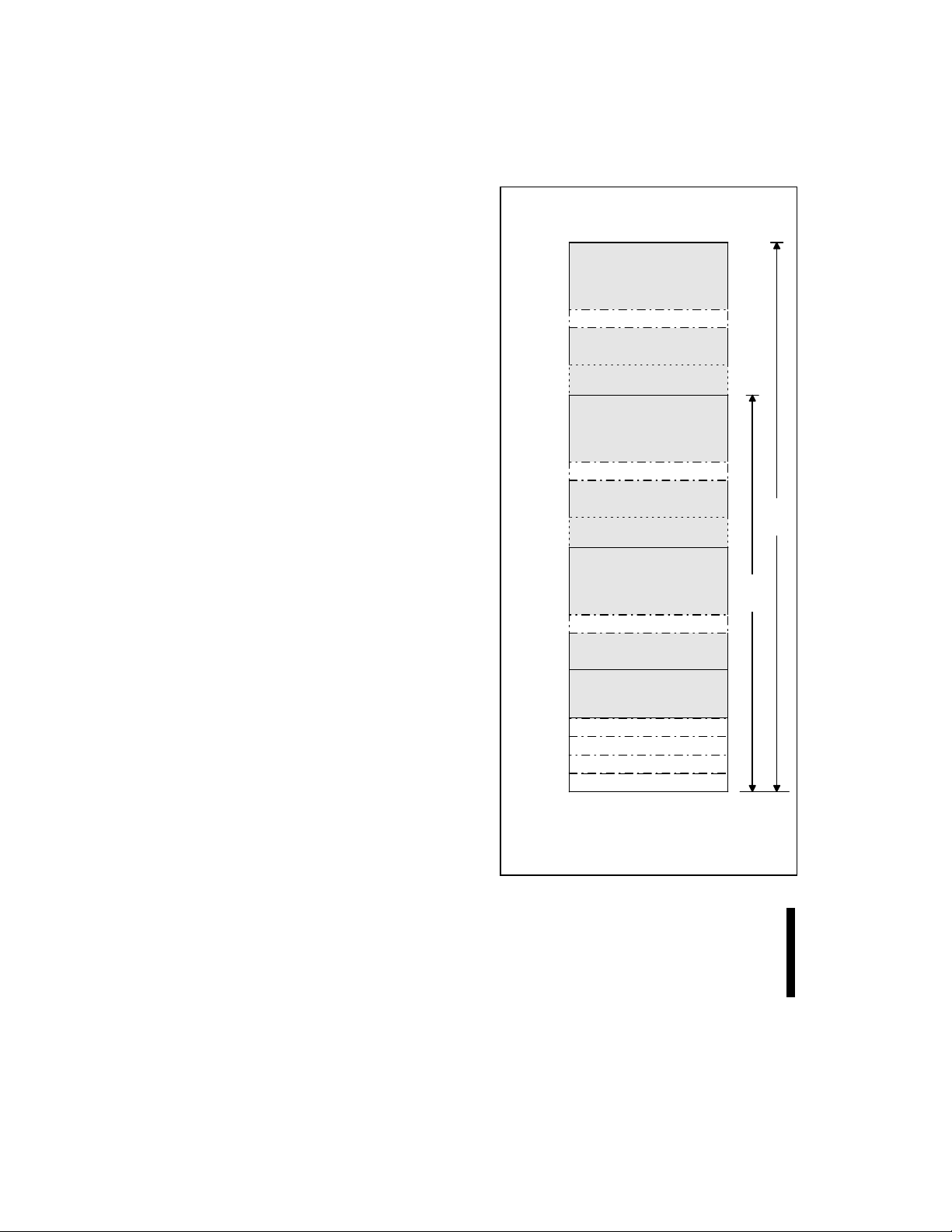
lock configuration code (see Figure 6). Using the
manufacturer and device codes, the system CPU
can automatically match t he device with its proper
algorithms. The block lock and master lock
configuration codes identify locked and unlocked
blocks and master lock-bit setting.
3.7 Write
Writing commands to the CUI enables reading of
device data, query, ident ifier codes, inspecti on and
clearing of the status register, and, when V
V
, block erasure, program, and lock-bit
PENH
PEN
=
configuration.
The Block Erase command requires appropriate
command data and an address within the block to
be erased. The Byte/Word Program command
requires the command and address of the location
to be written. Set Master and Block Lock-Bit
commands require the command and address
within the device (Master Loc k) or block within the
device (Block Lock ) to be locked. The Clear Block
Lock-Bits command requires the command and
address within the device.
The CUI does not occupy an address able memory
location. It is written when the device is enabled
and WE# is active. The addres s and data needed to
execute a command are latched on the risi ng edge
of WE# or the first edge of CE
disables the device (s ee Table 2,
Table
). Standard microprocessor write timings are
, CE1, or CE2 that
0
Chip Enable Truth
used.
4.0 COMMAND DEFINITIONS
When the V
operations from the status regi ster, query, identif ier
codes, or blocks are enabled. Placing V
14
voltage ≤ V
PEN
PENLK
, only read
on
PENH
additionally enables block erase, program,
PEN
and lock-bit configuration operations.
Device operations are selected by writing specific
commands into the CUI. Table 4 defines these
commands.
Word
Address
3FFFFF
3F0003
3F0002
3F0000
3EFFFF
1F0003
1F0002
1F0000
1EFFFF
01FFFF
010003
010002
010000
00FFFF
000004
000003
000002
000001
000000
NOTE:
A0 is not used in either x8 or x16 modes when obtaining
these identifier codes. Data is always given on the low byte
in x16 mode (upper byte contains 00h).
A[22-1]: 64 Mbit
A[21-1]: 32 Mbit
Block 63
Reserved for Future
Implementation
Block 63 Lock Configuration
Reserved for Future
Implementation
(Blocks 32 through 62)
Block 31
Reserved for Future
Implementation
Block 31 Lock Configuration
Reserved for Future
Implementation
(Blocks 2 through 30)
Block 1
Reserved for Future
Implementation
32 Mbit
Block 1 Lock Configuration
Reserved for Future
Implementation
Block 0
Reserved for Future
Implementation
Master Lock Configuration
Block 0 Lock Configuration
Device Code
Manufacturer Code
0606_06
Figure 6. Device Identifier Code Memory Map
ADVANCE INFORMATION
64 Mbit

E INTEL StrataFlash™ MEMORY TECHNOLOGY, 32 AND 64 MBIT
Table 3. Bus Operations
Mode Notes RP# CE
Read Array 1,2,3 VIH or
V
HH
Output
Disable
VIH or
V
HH
Standby VIH or
V
HH
Reset/PowerDown Mode
Read
Identifier
V
IL
V
or
IH
V
HH
(10)
0,1,2
Enabled V
Enabled V
Disabled X X X X High Z X
X X X X X High Z High Z
Enabled V
Codes
Read Query VIH or
Read Status
VIH or
(WSM off)
Read Status
VIH or
(WSM on)
Write 3,6,7 VIH or
NOTES:
1. Refer to
2. X can be V
3. In default mode, STS is V
4. See
5. See
6. Command writes involving block erase, program, or lock-bit configuration are reliably executed when V
7. Refer to Table 4 for valid D
8. DQ refers to DQ
9. High Z will be V
10. See Table 2 for valid CE configurations.
11. OE# and WE# should never be enabled simultaneously.
DC Characteristics
or VIH for control and address pins, and V
V
It is V
mode.
V
and should not be attempted.
IL
voltages.
PENH
when the WSM is not busy, in block erase suspend mode (with programming inactive), or reset/power-down
OH
Read Identifier Codes Command
Read Query Mode Command
is within specification. Block erase, program, or lock-bit configuration with VIH < RP# < VHH produce spurious results
CC
OH
OL
–DQ7 if BYTE# is low and DQ0–DQ15 if BYTE# is high.
0
with an external pull-up resistor.
Enabled V
V
HH
Enabled V
V
HH
Enabled V
V
HH
Enabled V
V
HH
. When V
when the WSM is executing internal block erase, program, or lock-bit configuration algorithms.
during a write operation.
IN
≤ V
PEN
section for read identifier code data.
section for read query data.
(11)
WE#
PENLK
V
V
V
V
V
V
V
or V
(11)
IH
IH
IH
IH
IH
IH
IL
Address V
PEN
XX D
X X High Z X
See
X Note 4 High Z
Figure 6
See
X Note 5 High Z
Table 7
XX D
XV
PENH
XX D
for V
. See
PENH
PEN
DC Characteristics
OE#
IL
IH
IL
IL
IL
IL
IH
, memory contents can be read, but not altered.
PENLK
DQ7 = D
DQ
15–8
DQ
DQ
6–0
(8)
OUT
OUT
OUT
= High Z
= High Z
IN
for V
PEN
= V
(default
mode)
High Z
PENLK
PENH
STS
(9)
(9)
(9)
(9)
X
and
and
ADVANCE INFORMATION
15

INTEL StrataFlash™ MEMORY TECHNOLOGY, 32 AND 64 MBIT E
Oper
(14)
(1)
Addr
(2)
Data
Table 4. Intel StrataFlash™ Memory Command Set Definitions
Command Scaleable
or Basic
Command
(15)
Set
Bus
Notes First Bus Cycle Second Bus Cycle
Cycles
Req'd.
Oper
(1)
Addr
(2)
Data
(3,4)
Read Array SCS/BCS 1 Write X FFH
Read Identifier
SCS/BCS ≥2 5 Write X 90H Read IA ID
Codes
Read Query SCS ≥ 2 Write X 98H Read QA QD
Read Status
SCS/BCS 2 6 Write X 70H Read X SRD
Register
Clear Status
SCS/BCS 1 Write X 50H
Register
Write to Buffer SCS/BCS > 2 7,8,9 Write BA E8H Write BA N
Word/Byte
Program
SCS/BCS 2 10,11 Write X 40H
Write PA PD
or
10H
Block Erase SCS/BCS 2 9,10 Write X 20H Write BA D0H
Block Erase
SCS/BCS 1 9,10 Write X B0H
Suspend
Block Erase
SCS/BCS 1 10 Write X D0H
Resume
Configuration SCS 2 Write X B8H Write X CC
Set Block Lock-Bit SCS 2 12 Write X 60H Write BA 01H
Clear Block Lock-
SCS 2 13 Write X 60H Write X D0H
Bits
Set Master Lock-
2 12,13 Write X 60H Write X F1H
Bit
(3,4)
16
ADVANCE INFORMATION
 Loading...