

Intel Corporation AS87C196CB-20, AS87C196CB, AN87C196CB-20, AN87C196CB Datasheet
*Other brands and names are the property of their respective owners.
Information in this document is provided in connection with Intel products. Intel assumes no liability whatsoever, including infringement of any patent or
copyright, for sale and use of Intel products except as provided in Intel’s Terms and Conditions of Sale for such products. Intel retains the right to make
changes to these specifications at any time, without notice. Microcomputer Products may have minor variations to this specification known as errata.
April 1996COPYRIGHT©INTEL CORPORATION, 1996 Order Number: 272405-004
87C196CA/87C196CB 20 MHz
ADVANCED 16-BIT CHMOS MICROCONTROLLER
WITH INTEGRATED CAN 2.0
Automotive
Y
High Performance CHMOS 16-Bit CPU
(up to 20 MHz Operation)
Y
Register-Register Architecture
Y
Up to 56 Kbytes of On-Chip EPROM
Y
Up to 1.5 Kbyte of On-Chip Register
RAM
Y
Up to 512 Bytes of Additional RAM
(Code RAM)
Y
Up to 16 Mbyte Linear Address Space
Y
Supports CAN (Controller Area
Network) Specification 2.0
Y
15 Message Objects of 8 Bytes Data
Length
Y
10-Bit A/D with Sample/Hold
Y
38 Prioritized Interrupts
Y
Up to Seven 8-Bit (60) I/O Ports
Y
Full Duplex Serial Port (SIO) with
Dedicated Baudrate Generator
Y
Full Duplex Synchronous Serial I/O
Port (SSIO)
Y
Interprocessor Communication Slave
Port
Y
Selectable Bus Timing Modes for
Flexible Interfacing
Y
Oscillator Fail Detection Circuitry
Y
High Speed Peripheral Transaction
Server (PTS)
Y
Two Dedicated 16-Bit High-Speed
Compare Registers
Y
High Speed Capture/Compare (EPA)
Y
Two Flexible 16-Bit Timer Counters
Y
Flexible 8-/16-Bit External Bus
(Programmable)
Y
Programmable Bus (HLD/HLDA)
Y
1.4 ms 16 x 16 Multiply
Y
2.4 ms 32/16 Divide
b
40§Ctoa125§C Ambient
Device Pins/Package EPROM Reg RAM Code RAM I/O EPA SIO SSIO CAN A/D
Address
Space
87C196CB 84-Pin PLCC 56K 1.5K 512b 56 10 Y Y Y 8 1 Mbyte
87C196CB 100-Pin QFP 56K 1.5K 512b 60 10 Y Y Y 8 16 Mbyte
87C196CA 68-Pin PLCC 32K 1.0K 256b 38 6 Y Y Y 6 64 Kbyte
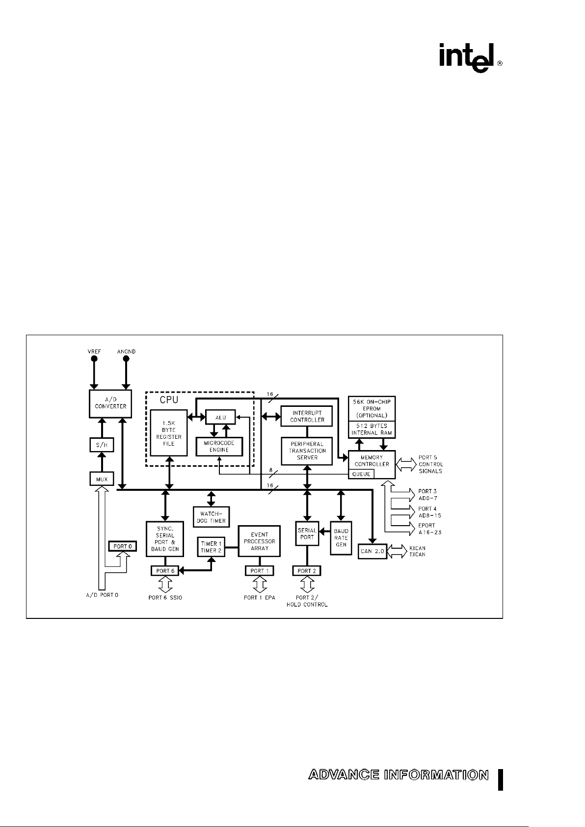
The 87C196CA/CB are new members of the MCSÉ96 microcontroller family. These devices are based upon
the MCS 96 Kx/Jx microcontroller product families with enhancements ideal for automotive and industrial
applications. The CA/CB are the first devices in the Kx family to support networking through the integration of
the CAN 2.0 (Controller Area Network) peripheral on-chip. The 87C196CB offers the highests memory density
of the MCS 96 microcontroller family, with 56K of on-chip EPROM, 1.5K of on-chip register RAM, and 512
bytes of additional RAM (Code RAM). In addition, the 87C196CB provides up to 16 Mbyte of Linear Address
Space. The 87C196CA is a sub-set of the CB, offering 32K of on-chip EPROM, up to 1.0K of on-chip register
RAM, and 256 bytes of additional RAM (Code RAM).
87C196CA/87C196CB
The MCS 96 microcontroller family members are all high-performance microcontrollers with a 16-bit CPU. The
87C196CB is composed of the high-speed (20 MHz) macrocore with up to 16 Mbyte linear address space, 56
Kbytes of program EPROM, up to 1.5 Kbytes of register RAM, and up to 512 bytes of code RAM (16-bit
addressing modes) with the ability to execute from this RAM space. It supports the high-speed, serial communications protocol CAN 2.0, with 15 message objects of 8 bytes data length, an 8-channel, 10-bit/3LSB
analog to digital converter with programmable S/H times, and conversion times
k
20 ms at 20 MHz. It has an
asynchronous/synchronous serial I/O port (SIO) with a dedicated 16-bit baud rate generator, an additional
synchronous serial I/O port (SSIO) with full duplex master/slave transceivers, a flexible timer/counter structure with prescaler, cascading, and quadrature capabilities. There are ten modularized, multiplexed, highspeed I/O for capture and compare (called Event Processor Array) with 200 ns resolution and double buffered
inputs, and a sophisticated prioritized interrupt structure with programmable Peripheral Transaction Server
(PTS) implementing several channel modes, including single/burst block transfers from any memory location
to any memory location, a PWM and PWM toggle mode to be used in conjunction with the EPA , and an A/D
scan mode.
NOTICE:
This is an advance information data sheet. The A.C. and D.C. parameters contained within this data
sheet may change after full automotive temperature characterization of the device has been performed. Contact your local sales office before finalizing the timing and D.C. characteristics of a design
to verify you have the latest information.
272405–30
Figure 1. 8XC196CB Block Diagram
2
87C196CA/87C196CB
PROCESS INFORMATION
These devices are manufactured on P629.5, a
CHMOS III-E process. Additional process and reliability information is available in Intel’s
Components
Quality and Reliability Handbook
, Order Number
210997.
All thermal impedance data is approximate for static
air conditions at 1.0W of power dissipation. Values
will change depending on operation conditions and
application. See the Intel
Packaging Handbook
(order number 240800) for a description of Intel’s thermal impedance test methodology.
272405–2
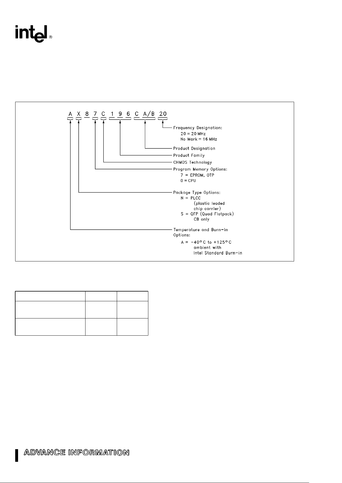
Figure 2. The 87C196CA/CB Familiy Nomenclature
Thermal Characteristics
Device and Package i
JA
i
JC
AN87C196CB 35.0§C/W 11.0§C/W
(84-Lead PLCC Package)
AN87C196CA 36.5§C/W 10.0§C/W
(68-Lead PLCC Package)
NOTES:
1. i
JA
e
Thermal resistance between junction and the surrounding environment (ambient) measurements are taken 1 ft.
away from case in air flow environment.
i
JC
e
Thermal resistance between junction and package face (case).
2. All values of i
JA
and iJCmay fluctuate depending on the environment (with or without airflow, and how much airflow)
and device power dissipation at temperature of operation. Typical variations are
g
2§C/W.
3. Values listed are at a maximum power dissipation of 1.0W.
3
87C196CA/87C196CB
272405–14
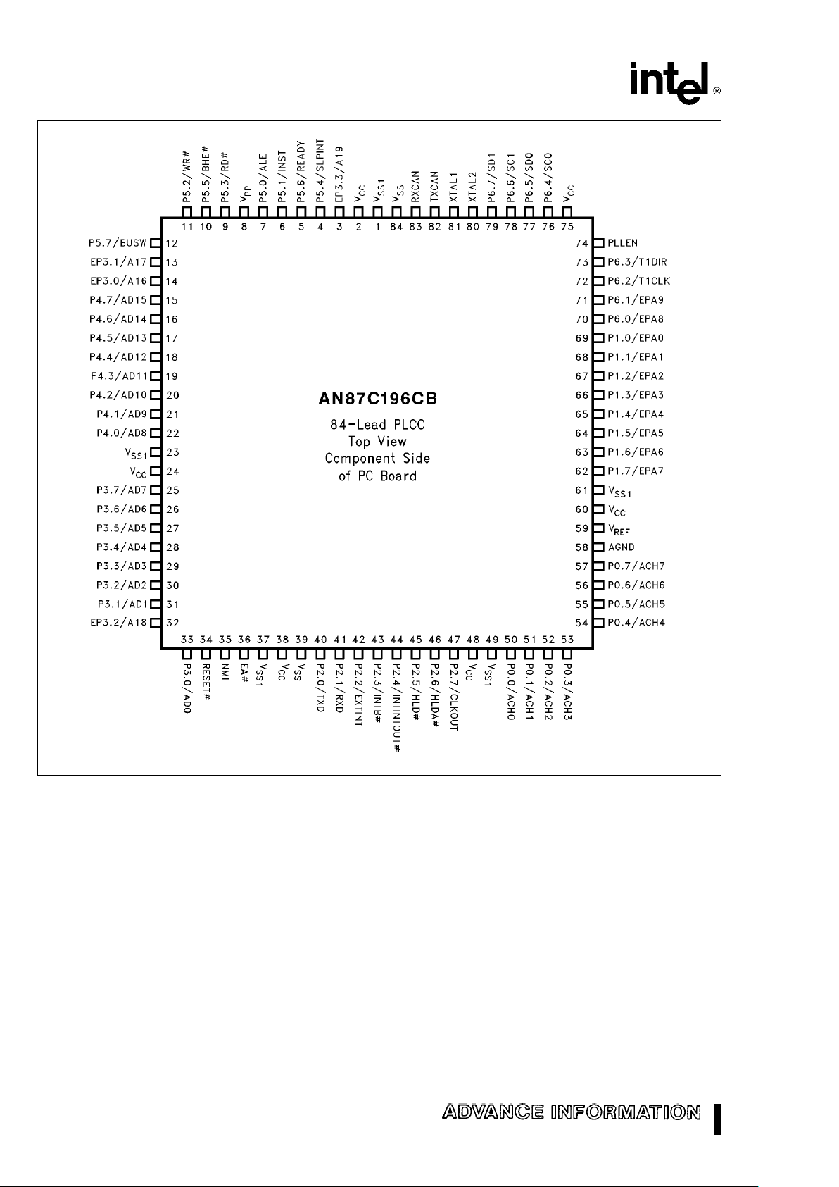
Figure 3. 84-Pin PLCC AN87C196CB Diagram
4
87C196CA/87C196CB
272405–33
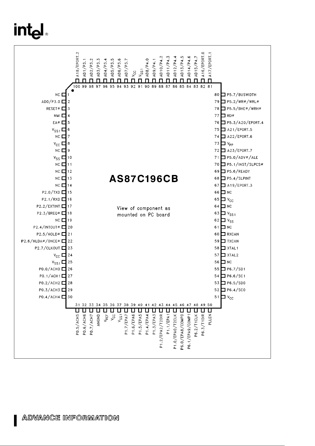
Figure 4. 100-Pin QFP AS87C196CB Diagram
5
87C196CA/87C196CB
272405–3
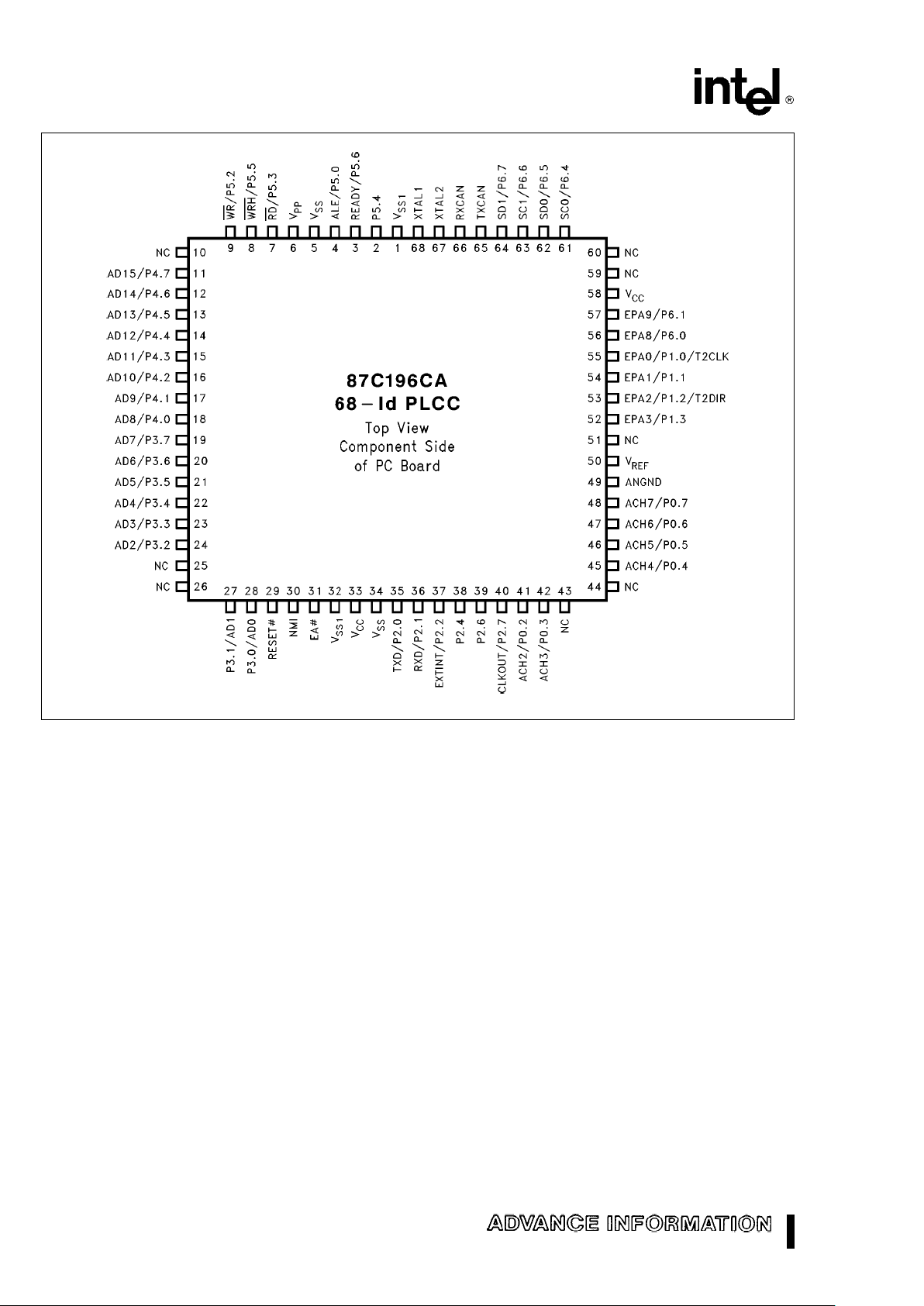
Figure 5. 68-Pin PLCC 87C196CA Diagram
6
87C196CA/87C196CB
Symbol Name and Function
V
CC
Main Supply Voltage (a5V).
VSS,V
SS1
Digital circuit ground (0V). There are 7 VSSpins CB (4 on CA), all of which MUST be
connected to a single ground plane.
V
REF
Reference for the A/D converter (a5V). V
REF
is also the supply voltage to the analog
portion of the A/D converter and the logic used to read Port 0. Must be connected for
A/D and Port 0 to function.
ANGND Reference ground for the A/D converter. Must be held at nominally the same potential
as V
SS
.
V
PP
Programming voltage for EPROM parts. It should bea12.5V for programming. It is
also the timing pin for the return from powerdown circuit. Connect this pin with a 1 mF
capacitor to V
SS
and a 1Mohm resistor to VCC. If this function is not used, VPPmay be
tied to VCC.
XTAL1 Input of the oscillator inverter and the internal clock generator.
XTAL2 Output of the Oscillator Inverter.
RESET
Ý
Reset input to the chip. Input low for at least 16 state times will reset the chip. The
subsequent low to high transition resynchronizes CLKOUT and commences a
10-state time sequence in which the PSW is cleared, bytes are read from 2018H,
201Ah and 201CH (if enabled) loading the CCB’s, and a jump to location 2080H is
executed. Input high for normal operation. RESETÝhas an internal pullup.
NMI A positive transition causes a non-maskable interrupt vector through memory location
203EH. If not used, this pin should be tied to V
SS
. May be used by Intel Evaluation
boards.
EA
Ý
Input for memory select (External Access). EAÝequal to a high causes memory
accesses to locations 0FF2000H through 0FFFFFFH to be directed to on-chip
EPROM/ROM. EA
Ý
equal to a low causes accesses to these locations to be directed
to off-chip memory. EA
Ý
ea
12.5V causes execution to begin in the Programming
Mode. EA
Ý
is latched at reset.
PLLEN Selects between PLL mode or PLL bypass mode. This pin must be either tied high or
low. PLLEN pin
e
0, bypass PLL mode. PLLEN pine1, places a 4x PLL at the input
(196CB only)
of the crystal oscillator. Allows for a low frequency crystal to drive the device (i.e.,
5 MHz
e
20 MHz operation).
P6.4– 6.7/SSIO Dual function I/O ports have a system function as Synchronous Serial I/O. Two pins
are clocks and two pins are data providing for full duplex capability. Also LSIO when
not used as SSIO.
P6.3/T1DIR Dual function I/O pin. Primary function is that of a bidirectional I/O pin, however, it
may also be used as a TIMER1 Direction input. The TIMER1 will increment when this
(CB only)
pin is high and decrements when this pin is low.
P6.2/T1CLK Dual function I/O pin. Primary function is that of a bidirectional I/O pin, however may
also be used as a TIMER1 Clock input. The TIMER1 will increment or decrement on
(CB only)
both positive and negative edges of this pin.
P6.0– 6.1/EPA8 –9 Dual function I/O port pins. Primary function is that of bidirectional I/O. System
function is that of High Speed capture and compare.
7
87C196CA/87C196CB
Symbol Name and Function
P5.7/BUSWIDTH Input for bus width selection. If CCR bit 1 is a one and CCR1 bit 2 is a one, this pin
dynamically controls the Buswidth of the bus cycle in progress. If BUSWIDTH is low,
(CB only)
an 8-bit cycle occurs, if BUSWIDTH is high, a 16-bit cycle occurs. If CCR bit 1 is ‘‘0’’
and CCR1 bit 2 is ‘‘1’’, all bus cycles are 8-bit, if CCR bit 1 is ‘‘1’’ and CCR1 bit 2 is
‘‘0’’, all bus cycles are 16-bit. CCR bit 1
e
‘‘0’’ and CCR1 bit 2e‘‘0’’ is illegal. Also
an LSIO pin when not used as BUSWIDTH.
P5.6/READY Ready input to lengthen external memory cycles, for interfacing with slow or dynamic
memory, or for bus sharing. If the pin is high, CPU operation continues in a normal
manner. If the pin is low prior to the falling edge of CLKOUT, the memory controller
goes into a wait state mode until the next opositive transition in CLKOUT occurs with
READY high. When external memory is not used, READY has no effect. The max
number of wait states inserted into the bus cycle is controlled by the CCR/CCR1.
Also an LSIO if READY is not selected.
P5.5/BHEÝ/WRHÝByte High Enable or Write High output, as selected by the CCR. BHE
Ý
e
0 selects
the bank of memory that is connected to the high byte of the data bus. A0
e
0
selects the bank of memory that is connected to the low byte. Thus accesses to a
16-bit wide memory can be to the low byte only (A0
e
0, BHE
Ý
e
1), to the high
byte only (A0
e
1, BHE
Ý
e
0) or both bytes (A0e0, BHE
Ý
e
0). If the WRH
Ý
function is selected, the pin will go low if the bus cycle is writing to an odd memory
location. BHE
Ý
/WRHÝis only valid during 16-bit external. Also an LSIO pin when
not BHE/WRH
Ý
.
P5.4/SLPINT Dual function I/O pin. As a bidirectional port pin or as a system function. The system
function is a Slave Port Interrupt Output Pin (on CA, bidirectional port pin only).
P5.3/RD
Ý
Read signal output to external memory. RDÝis active only during external memory
reads or LSIO when not used as RD
Ý
.
P5.2/WRÝ/WRL
Ý
Write and Write Low output to external memory, as selected by the CCR, WRÝwill
go low for every external write, while WRL
Ý
will go low only for external writes where
an even byte is being written. WRÝ/WRLÝis active during external memory writes.
Also an LSIO pin when not used as WR
Ý
/WRLÝ.
P5.1/INST Output high during an external memory read indicates the read is an instruction
fetch. INST is valid throughout the bus cycle. INST is active only during external
(CB only)
memory fetches, during internal EPROM fetches INST is held low. Also LSIO when
not INST.
P5.0/ALE/ADV
Ý
Address Latch Enable or Address Valid Output, as selected by CCR. Both pin
options provide a latch to demultiplex the address from the address/data bus. When
the pin is ADV
Ý
, it goes inactive (high) at the end of the bus cycle. ADVÝcan be
used as a chip select for external memory. ALE/ADV
Ý
is active only during external
memory accesses. Also LSIO when not used as ALE.
8
87C196CA/87C196CB
Symbol Name and Function
PORT 3 and 4 8-bit bidirectional I/O ports with open drain outputs. These pins are shared with the
multiplexed address/data bus which has strong internal pullups.
P2.7/CLKOUT Output of the internal clock generator. The frequency is the oscillator frequency.
CLKOUT has a 50% duty cycle. Also LSIO pin when not used as CLKOUT.
P2.6/HLDA
Ý
Bus Hold Acknowledge. Active-low output indicates that the bus controller has
relinquished control of the bus. Occurs in response to an external device asserting the
HLD
Ý
signal. Also LSIO when not used as HLDAÝ.
P2.5/HLD
Ý
Bus Hold. Active-low signal indictes that an external device is requesting control of the
bus. Also LSIO when not used as HLD
Ý
.
(CB only)
P2.4/INTOUT
Ý
Interrupt Output. This active-low output indicates that a pending interrupt requires use
of the external bus. Also LSIO when not used as INTOUT
Ý
P2.3/BREQ
Ý
Bus Request. This active-low output signal is asserted during a HOLD cycle when the
bus controller has a pending external memory cycle. Also LSIO when not used as
(CB only)
BREQ
Ý
P2.2/EXTINT A positive transition on this pin causes a maskable interrupt vector through memory
location 203CH. Also LSIO when not used as EXTINT.
P2.1/RXD Receive data input pin for the Serial I/O port. Also LSIO if not used as RXD.
P2.0/TXD Transmit data output pin for the Serial I/O port. Also LSIO if not used as TXD.
PORT 1/EPA0 – 7 Dual function I/O port pins. Primary function is that of bidirectional I/O. System function
is that of High Speed capture and compare. EPA0 and EPA2 have another function of
T2CLK and T2DIR of the TIMER2 timer/counter.
PORT 0/ACH0 – 7 8-bit high impedance input-only port. These pins can be used as digital inputs and/or as
analog inputs to the on-chip A/D converter. These pins are also used as inputs to
EPROM parts to select the Programming Mode.
EPORT 8-bit bidirectional standard and I/O Port. These bits are shared with the extended
address bus, A16 –A19 for CB PLCC, A16 –A23 for CB QFP. Pin function is selected on
(CB only)
a per pin basis.
TXCAN Push-pull output to the CAN bus line.
RXCAN High impedance input-only from the CAN bus line.
9
87C196CA/87C196CB
87C196CB Memory Map
Address Description
FFFFFFH Program Memory - Internal EPROM or External Memory
FF2080H (Determined by EA
Ý
Pin)
FF207FH Special Purpose Memory (Internal EPROM or External Memory)
FF2000H (Determined by EA
Ý
Pin)
FF1FFFH External Memory
FF0600H
FF05FFH Internal RAM (Identically Mapped into 00400H– 005FFH)
FF0400H
FF03FFH External Memory
FF0100H
FF00FFH Reserved for ICE
FF0000H
FEFFFFH Overlayed Memory (External)ÐAccesses into Memory Ranges 0F0000H to FEFFFFH will
Overlay Page 15 (0FH) for CB QFP packageÐExternal Memory.
(5)
0F0000H
0EFFFFH 900 Kbytes External Memory
010000H
00FFFFH External Memory or Remapped OTPROM (Program Memory)
(1)
002080H
00207FH External Memory or Remapped OTPROM (Special Purpose Memory)
(1, 3)
002000H
001FFFH Memory Mapped Special Function Registers (SFR’s)
001FE0H
001FDFH Internal Peripheral Special Function Registers (SFR’s)
(5)
001F00H
001EFFH Internal CAN Peripheral Memory
(5)
001E00H
001DFFH Internal Register RAM
001C00H
001BFFH External Memory
000600H
0005FFH Internal RAM (Code RAM)
000400H (Address with Indirect or Indexed Modes)
0003FFH Register RAM – Upper Register File (Address with Indirect or Indexed Modes or through
Windows.)
(2)
000100H
10
 Loading...