Intel Corporation AN87C196LB-20, AN87C196LB Datasheet

Intel Corporation assumes no responsibility for the use of any circuitry other than circuitry embodied in an Intel product. No other circuit patent
licenses are implied. Information contained herein supersedes previously published specifications on these devices from Intel.
© INTEL CORPORATION, 1996 Februa ry 1996 Order Number: 272807-000
®
PRODUCT PREVIEW
87C196LB
CHMOS 16-BIT MICROCONTROLLER
Automotive
NOTE
This datasheet contains information on products in the design phase of development. The
specifi catio ns are subj ect to change without notice. Veri fy with your local Inte l sales office
that you have the latest datasheet before finalizing a design.
The 87C196LB is a high-performance 16-bit microcontroller with integrated support for the J1850 communication
protocol. The 87C196LB is composed of a high-speed core with the following peripherals: an
asynchronous/synchronous serial I/O port (8096 compatible) with a dedicated 16-bit baud-rate generator; an
additional synchronous serial I/O port with full duplex master/slave transceivers; a six-channel A/D converter with
sample and hold; a flexi ble timer/coun ter structure with prescaler, casca ding, and quad rature capabili ties; six
modula rized, multiplexed hig h-speed I/O for capt ure and compare (cal led event proces sor array) with 200 n s
resolution and double buffered inputs; and a sophisticated prioritized interrupt structure with programmable
peripheral transaction server (PTS). The clo ck doubler circuitry and oscillator output sig nal enable a 4 MH z
resonator to achieve the same interna l clock speed as a more costly 8 MHz resonator in previo us applicati ons.
This same circuitry can drive other devices where a separate resonator was required in the past. Another costsavings feature is the fact that the I/O ports are driven low at reset, avoiding the need for pull-up resistors.
■ 20 MHz operation
†
■ 24 Kbytes of on-chip OTPROM
■ 768 bytes of on- chip register R AM
■ Register-to-register architecture
■ Peripheral transaction server (PTS)
with high-speed, microcoded interrupt
service routines
■ Integrated, industry-standard J1850
communication protocol
■ Six-channel/10-bit A/D with sample and
hold
■ High-speed event processor array
— Six capture/compare channels
— Two compare-only channels
— Two 16-bit software timers
†
16 MHz standard; 20 MHz is speed premium
■ Ful l- du p l ex s er i al I/O port wit h
dedicated baud-rate generator
■ Enhanced full-duplex, synchronous
serial I/O port (SSIO)
■ Programmable 8- or 16-bit external bus
■ Optional clock doubler with
programmable clock output signal
■ SFR register that indicates the source
of the last reset
■ Design enhancements for EMI
reduction
■ Oscillator failure detect ion circuit ry
■ Watchdog timer (WDT)
■ –40° C to +125° C ambient temperature
■ 52-pin PLCC package
PRODUCT PREVIEW
2
AUTOMOTIVE
®
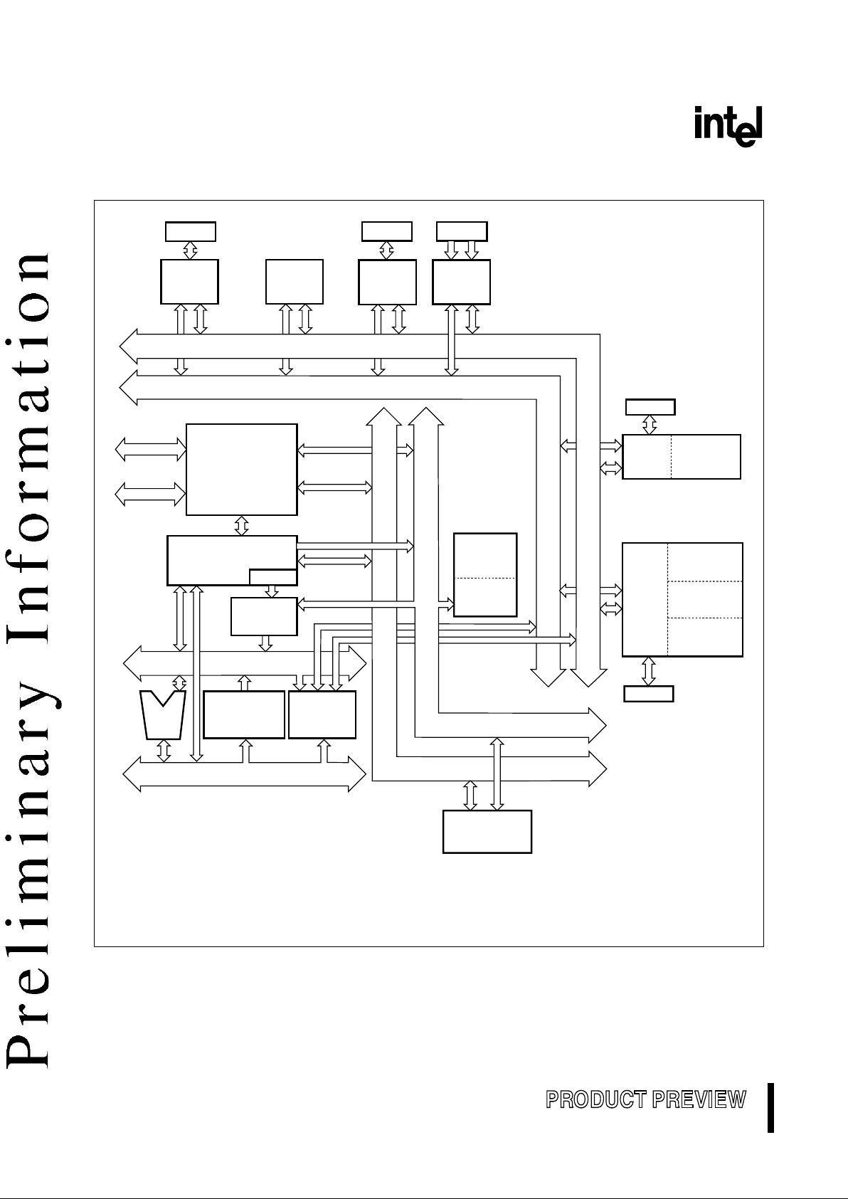
Figure 1. 87C196LB Block Diagram
Queue
Source (16)
Destination (16)
AD15:0
EPA
2 Timers
6 Capture/
Compare
Channels †
Bus
Controller
Watchdog
Timer
Enhanced
SSIO
OTPROM
24 Kbytes
A3416-01
SIO
Baud-rate
Generator
Port 6
Memory Data Bus (16)
Bus-Control
Interface Unit
Microcode
Engine
Peripheral
Transaction
Server
Memory
Interface
Unit
Register RAM
768 Bytes
ALU
Interrupt
Controller
Bus Control
Peripheral Addr Bus (10)
Peripheral Data Bus (16)
Memory Addr Bus (16)
2
Compare-only
Channels
Port 2
Port 1,6
Port 0
A/D
Converter
J1850
Protocol
Handler
† Two additional capture/compare channels (EPA6 and EPA7) are available as software timers.
Port 2
They are not connected to package pins.
3
AUTOMOTIVE
®
PRODUCT PREVIEW
1.0 NOMENCLATURE OVERVIEW
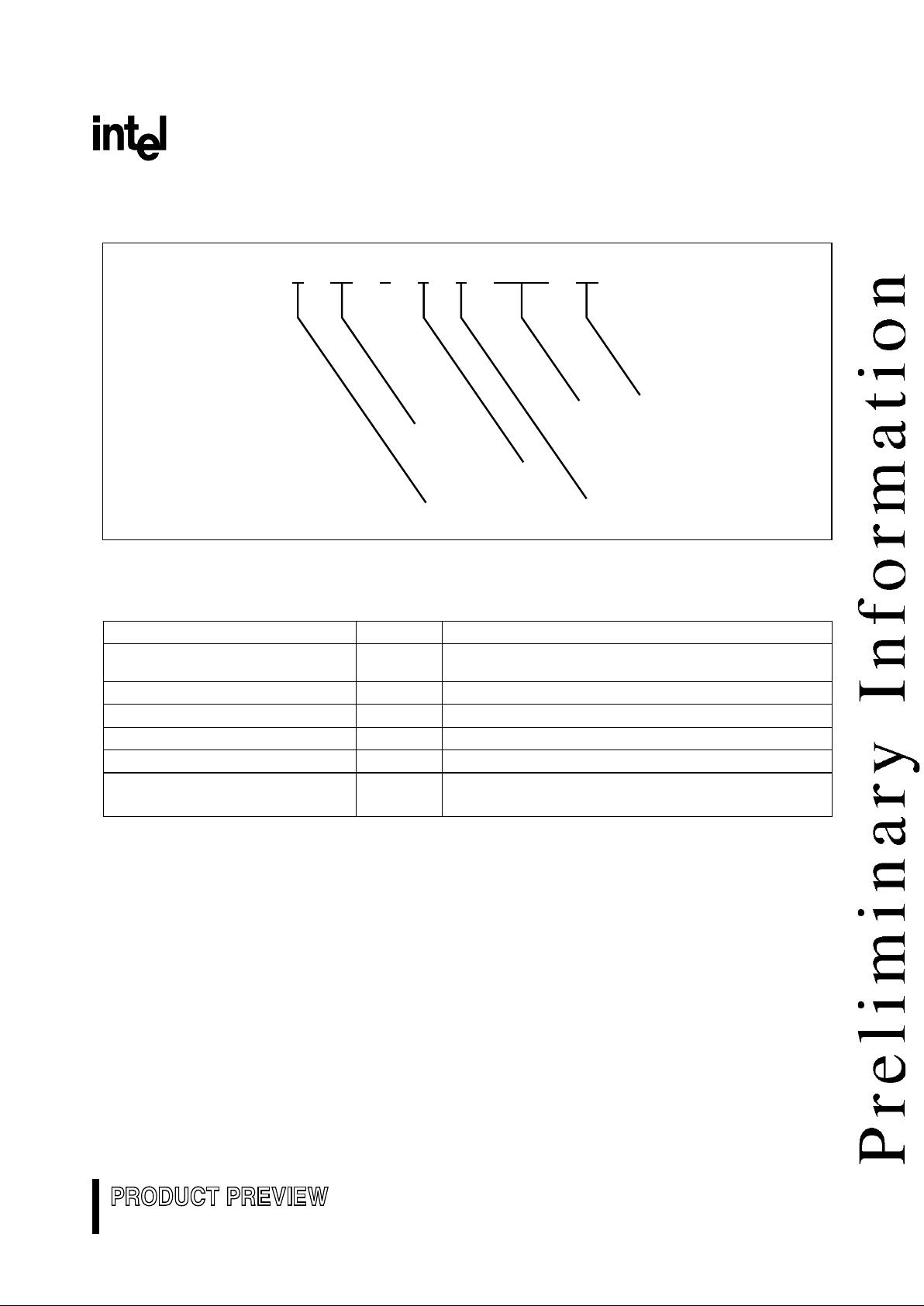
Figure 2. Produ ct Nom en cla ture
Table 1. Description of Product Nomenclature
Parameter Options Description
Tempe ra ture and Burn- in Opti on s A Automo ti ve operating tem pe rat ure rang e (–4 0° C to
125° C ambient) with Intel standard burn-in.
Packaging Options N PLCC
Prog ram-m em o r y Option s 7 OTPROM
Process Information C CHMOS
Product Family 196L
x
8XC196Lx family of products
Device Speed no mark2016 MHz
20 MHz
Program-memory Options
XXXXX XXXX8XXX
Packaging Options
Temperature and Burn-in Options
A2815-02
Process and Voltage Information
Product Family
Device Speed
PRODUCT PREVIEW
4
AUTOMOTIVE
®
2.0 PINOUT
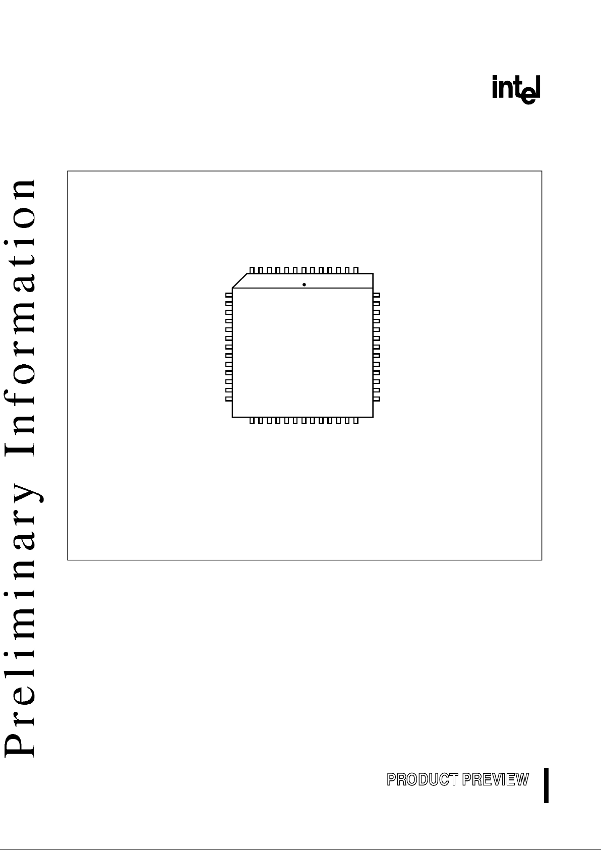
Figure 3. 87C19 6L B 52-pin P acka ge
P6.1 / EPA9 / COMP1
P6.0 / EPA8 / COMP0
P1.0 / EPA0 / T2CLK
P1.1 / EPA1
P1.2 / EPA2 / T2DIR
P1.3 / EPA3
V
REF
ANGND
P0.7 / ACH7 / PMODE.3
P0.6 / ACH6 / PMODE.2
P0.5 / ACH5 / PMODE.1
P0.4 / ACH4 / PMODE.0
P0.3 / ACH3
AD15 / P4.7 / PBUS.15
P5.2 / PLLEN /WR# / WRL#
P5.3 / RD#
V
PP
V
SS
(core)
P5.0 / ADV# / ALE
V
SS1
(port)
XTAL1
XTAL2
P6.7 / SD1
P6.6 / SC1
P6.5 / SD0
P6.4 / SC0
A3361-01
AD14 / P4.6 / PBUS.14
AD13 / P4.5 / PBUS.13
AD12 / P4.4 / PBUS.12
AD11 / P4.3 / PBUS.11
AD10 / P4.2 / PBUS.10
AD9 / P4.1 / PBUS.9
AD8 / P4.0 / PBUS.8
AD7 / P3.7 / PBUS.7
AD6 / P3.6 / PBUS.6
AD5 / P3.5 / PBUS.5
AD4 / P3.4 / PBUS.4
AD3 / P3.3 / PBUS.3
AD2 / P3.2 / PBUS.2
46
45
44
43
42
41
40
39
38
37
36
35
34
AN87C196LB
View of component as
mounted on PC board
8
9
10
11
12
13
14
15
16
17
18
19
20
AD1 / P3.1 / PBUS.1
AD0 / P3.0 / PBUS.0
RESET#
EA#
V
SS1
(port)
V
CC
P2.0 / TXD / PVER
P2.1 / RXD / PALE#
P2.2 / EXTINT / PROG#
P2.4 / RXJ1850 / AINC#
P2.6/TXJ1850 / CPVER
P2.7 / CLKOUT / PACT#
P0.2 / ACH2
21
22
23
24
25
26
27
28
29
30
31
32
33
7654321
52
51
50
49
48
47
5
AUTOMOTIVE
®
PRODUCT PREVIEW
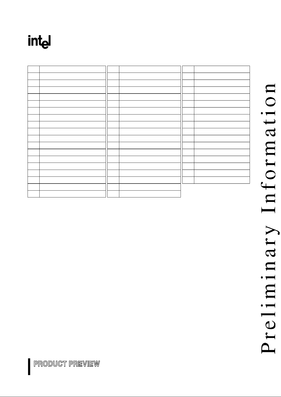
Table 2. 87C196LB 52-pin Package Pin Assignments
Pin Name Pin Name Pin Name
1V
SS1
(port) 19 AD3 / P3.3 / PBUS.3 37 P0.6 / ACH6 / PMODE.2
2 P5.0 / ADV# / ALE 20 AD2 / P3.2 / PBUS.2 38 P0.7 / ACH7 / PMODE.3
3V
SS
(core) 21 AD1 / P3.1 / PBUS.1 39 ANGND
4V
PP
22 AD0 / P3.0 / PBUS.0 40 V
REF
5 P5.3 / RD# 23 RESET# 41 P1.3 / EPA3
6 P5.2 / PLLEN / WR# / WRL# 24 EA# 42 P1.2 / EPA2 / T2DIR
7 AD15 / P4.7 / PBUS.15 25 V
SS1
(port) 43 P1.1 / EPA1
8 AD14 / P4.6 / PBUS.14 26 V
CC
44 P1.0 / EPA0 / T2CLK
9 AD13 / P4.5 / PBUS.13 27 P2.0 / TXD / PVER 45 P6.0 / EPA8 / COMP0
10 AD12 / P4.4 / PBUS.12 28 P2.1 / RXD / PALE# 46 P6.1 / EPA9 / COMP1
11 AD11 / P4.3 / PBUS.11 29 P2.2 / EXTINT / PROG# 47 P6.4 / SC0
12 AD10 / P4.2 / PBUS.10 30 P2.4 / RXJ1850 / AINC# 48 P6.5 / SD0
13 AD9 / P4.1 / PBUS.9 31 P2.6 / TXJ1850 / CPVER 49 P6.6 / SC1
14 AD8 / P4.0 / PBUS.8 32 P2.7 / CLKOUT / PACT# 50 P6.7 / SD1
15 AD7 / P3.7 / PBUS.7 33 P0.2 / ACH2 51 XTAL2
16 AD6 / P3.6 / PBUS.6 34 P0.3 / ACH3 52 XTAL1
17 AD5 / P3.5 / PBUS.5 35 P0.4 / ACH4 / PMODE.0
18 AD4 / P3.4 / PBUS.4 36 P0.5 / ACH5 / PMODE.1
PRODUCT PREVIEW
6
AUTOMOTIVE
®
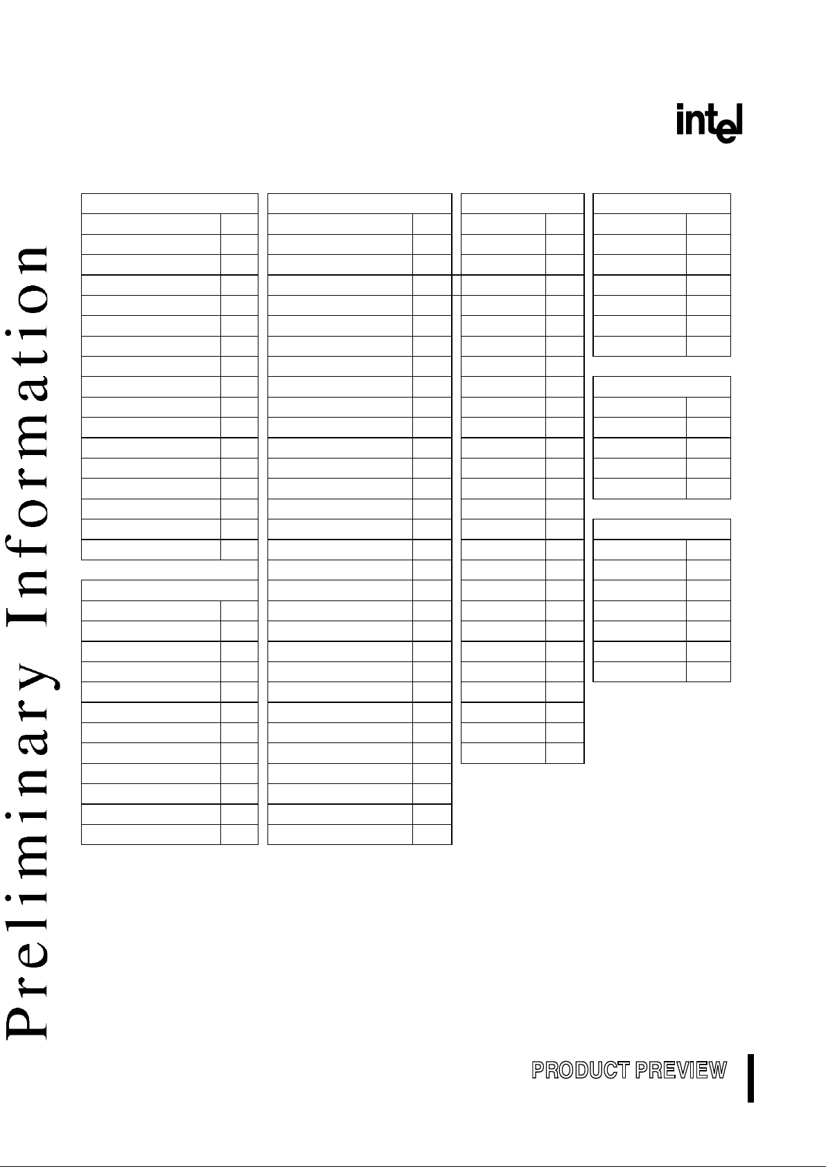
Table 3. Pin Assignment Arranged by Functional Categories
Addr & Data Input/Output (Cont’d) Program Control Processor Control
Name Pin Name Pin Name Pin Name Pin
AD0 22 P2.1 / RXD 28
AINC# 30 EA# 24
AD1 21 P2.2 29 CPVER 31
EXTINT 29
AD2 20
P2.4 / RXJ1850 30 PACT# 32 PLLE N 6
AD3 19
P2.6 / TXJ1850 31 PALE# 28 RESET# 23
AD4 18
P2.7 32 PBUS.0 22 XTAL1 52
AD5 17 P3.0 22 PBUS.1 21
XTAL2 51
AD6 16
P3.1 21 PBUS.2 20
AD7 15 P3.2 20 PBUS.3 19 Bus Cont & Status
AD8 14 P3.3 19 PBUS.4 18
Name Pin
AD9 13 P3.4 18 PBUS.5 17
ADV# / ALE 2
AD10 12 P3.5 17 PBUS.6 16
CLKOUT 32
AD11 11 P3.6 16 PBUS.7
15 RD# 5
AD12 10 P3.7 15 PBUS.8
14 WR# / WRL# 6
AD13 9 P 4.0 14 PBUS.9
13
AD14 8 P 4.1 13 PBUS.10 12 Power & Ground
AD15 7 P4.2 12 PBUS.1 1
11 Name Pin
P4.3 11 PBUS.12
10 ANGND 39
Input/Outp ut P4.4 10 PBUS.13 9
V
CC
26
Name Pin P4.5 9 PBUS.14 8
V
PP
4
P0.2 / ACH2 33 P4.6 8 PBUS.15 7
V
REF
40
P0.3 / ACH3 34 P4.7 7 PMODE.0 35
VSS (core) 3
P0.4 / ACH4 35
P5.0 2 PMODE.1 36 V
SS1
(port) 1, 25
P0.5 / ACH5 36
P5.2 6 PMODE.2 37
P0.6 / ACH6 37 P5.3 5 PMODE.3 38
P0.7 / ACH7 38 P6.0 / EPA8 / COMP0 45 PROG# 29
P1.0 / EPA0 / T2CLK 44 P6.1 / EPA9 / COMP1 46 PVER 27
P1.1 / EPA1 43 P6.4 / SC0 47
P1.2 / EPA2 / T2DIR 42 P6.5 / SD0 48
P1.3 / EPA3 41 P6.6 / SC1 49
P2.0 / TXD 27 P6.7 / SD1 50
 Loading...