PRODUCT PREVIEW
COPYRIGHT © INTEL CORPORATION, 1996 October 1996 Order Number: 272806-001
87C196LA
CHMOS 16-BIT MICROCONT R O LLER
Automotive
NOTE
This datasheet contains information on products in the design phase of development.
The specifications are subject to change without notice. Verify with your local Intel sales
office that you have the latest datasheet before finalizing a design.
The 87C196LA is a high-performance 16-bit microcontroller. The 87C196LA is composed of a high-speed
core with the following peripherals: an asynchronous/synchronous serial I/O port (8096 compatible) with a
dedicated 16-bit baud-rate generator; an additional synchronous serial I/O port with full duplex master/slave
transceivers; a six-channel A/D converter with sample and hold; a flexible timer/counter structure with
prescaler, cascading, and quadrature capabilities; six modularized, multiplexed high-speed I/O for capture
and compare (called event processor array) with 200 ns resolution and double buffered inputs; and a sophisticated, prioritized interrupt structure with programmable peripheral transaction server (PTS). The clock
doubler circuitry and oscillator output signal enable a 4 MHz resonator to achieve the same internal clock
speed as a more costly 8 MHz resonator in previous applications. This same circuitry can drive other devices
where a separate resonator was required in the past. Another cost-savings feature is the fact that the I/O
ports are driven low at reset, avoiding the need for pull-up resistors.
■ 20 MHz operation
†
■ 24 Kbytes of on-chip OTPROM
■ 768 bytes of on-chip register RAM
■ Register-to-register architecture
■ Peripheral transaction server (PTS)
with high-speed, microcoded interrupt
service routines
■ Six-channel/10-bit A/D w ith sam ple and
hold
■ High-speed event processor array
—Six capture/compare channels
—Two compare-only channels
— Two 16-bit software timers
†
16 MHz standard; 20 MHz is speed premium
■ Full-duplex serial I/O port with
dedicated baud-rate generator
■ Enhanced full-duplex, synchronous
serial I/O port (SSIO)
■ Programmable 8- or 16-bit external bus
■ Optional clock doubler with
programmable clock output signal
■ SFR register that indicates the source
of the last reset
■ Design enhancements for EMI
reduction
■ Oscillator failure detection circuitry
■ Watchdog timer (WDT)
■ –40° C to +125° C ambient temperature
■ 52-pin PLCC package

Information in this document is provided in connection with Intel products. No license, express or implied, by
estoppel or otherwise, to any intellectual property rights is granted by this document. Except as provided in
Intel’s Terms and Conditions of Sale for such products, Intel assumes no liability whatsoever, and Intel disclaims any express or implied warranty, relating to sale and/or use of Intel products including liability or warranties relating to fitness for a particular purpose, merchantability, or infringement of any patent, copyright or
other intellectual property right. Intel products are not intended for use in medical, life saving, or life sustaining
applications.
Intel retains the right to make changes to specifications and product descriptions at any time, without notice.
*Third-party brands and names are the property of their respective owners.
Copies of documents which have an ordering number and are referenced in this document, or other Intel liter-
ature, may be obtained from:
Intel Corporation
P.O. Box 7641
Mt. Prospect, IL 60056-7641
or call 1-800-548-4725

PRODUCT PREV IEW 3
AUTOMOTIVE — 87C196LA
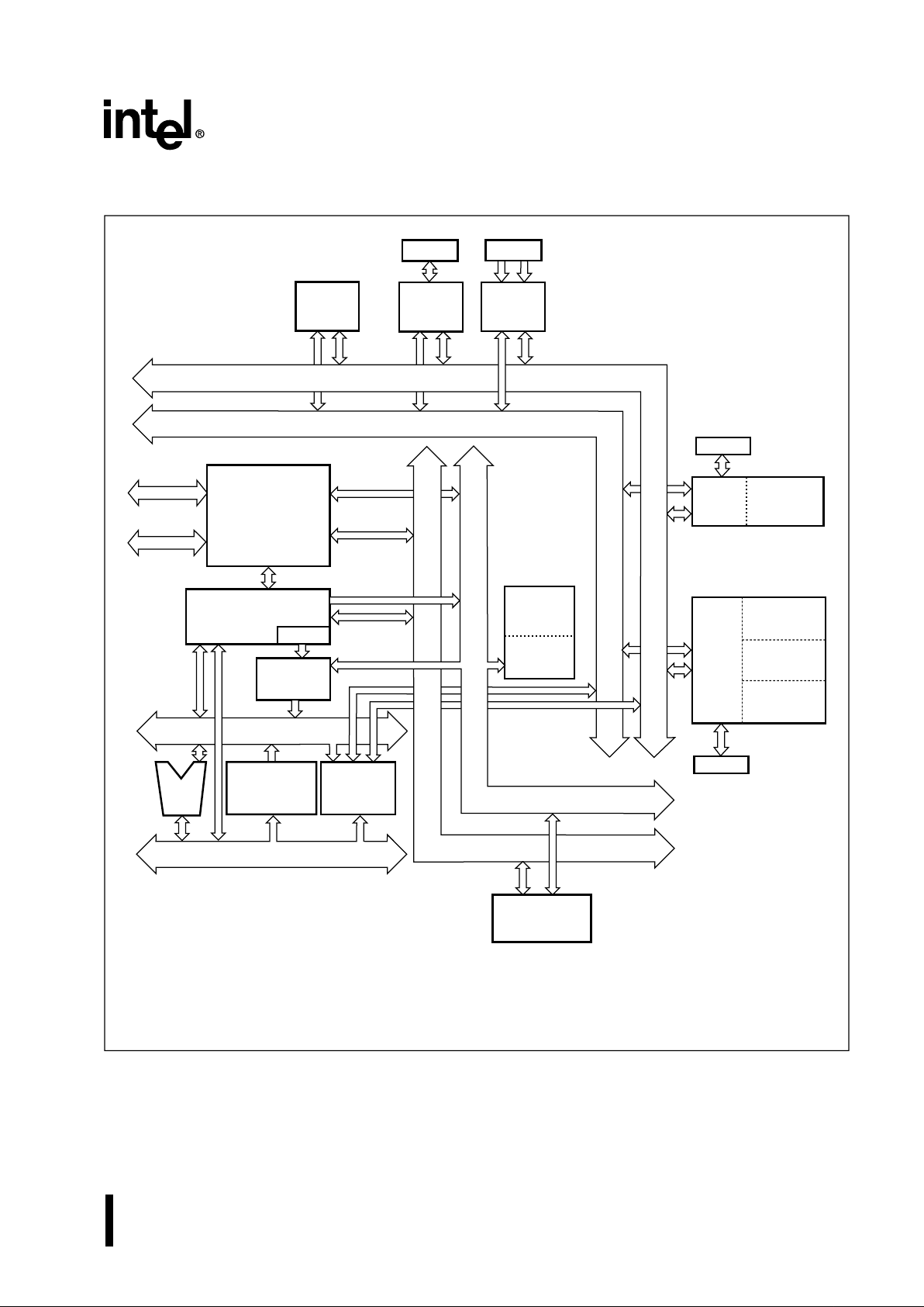
Figure 1. 87C196LA Block Diagram
Queue
Source (16)
Destination (16)
AD15:0
EPA
2 Timers
6 Capture/
Compare
Channels †
Bus
Controller
Watchdog
Timer
Enhanced
SSIO
OTPROM
24 Kbytes
A3417-01
SIO
Baud-rate
Generator
Port 6
Memory Data Bus (16)
Bus-Control
Interface Unit
Microcode
Engine
Peripheral
Transaction
Server
Memory
Interface
Unit
Register RAM
768 Bytes
ALU
Interrupt
Controller
Bus Control
Peripheral Addr Bus (10)
Peripheral Data Bus (16)
Memory Addr Bus (16)
2
Compare-only
Channels
Port 2
Port 1,6
Port 0
A/D
Converter
† Two additional capture/compare channels (EPA6 and EPA7) are available as software timers.
They are not connected to package pins.

4 PRODUCT PREVIEW
87C196LA — AUTOMOTIVE
1.0 NOMENCLATURE OVERVIEW
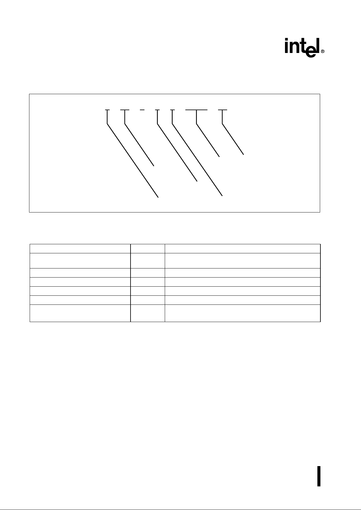
Figure 2. Product Nomenclature
Table 1. Description of Product Nomenclature
Parameter Options Description
Temperature and Burn-in Options A Automotive operating temperature range (–40° C to
125° C ambient) with Intel standard burn-in.
Packaging Options N PLCC
Program-memory Options 7 OTPROM
Process Information C CHMOS
Product Family 196L
x
8XC196Lx family of products
Device Speed no mark2016 MHz
20 MHz
Program Memory Options
XXXXX XXXX8XXX
Packaging Options
Temperature and Burn-in Options
A2815-02
Process and Voltage Information
Product Family
Device Speed

PRODUCT PREV IEW 5
AUTOMOTIVE — 87C196LA
2.0 PINOUT
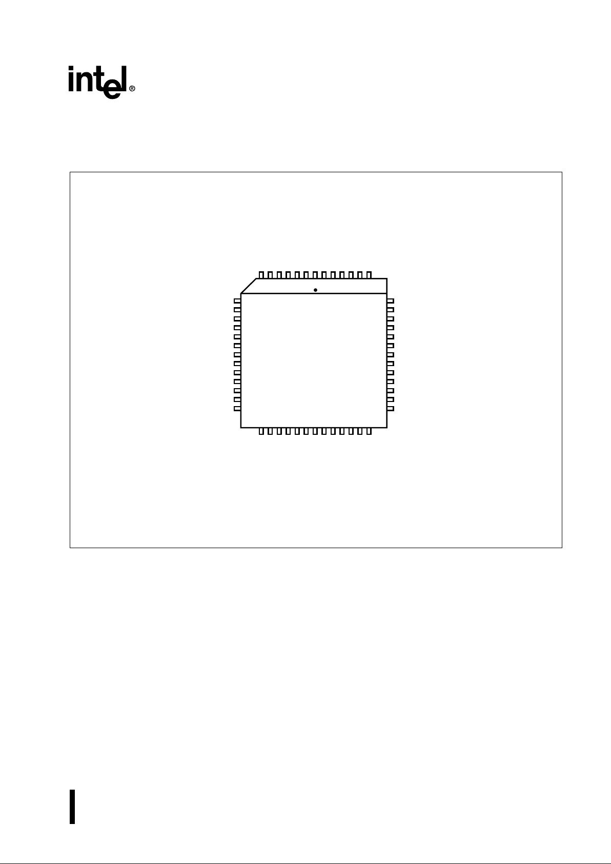
Figure 3. 87C196LA 52-pin Package
P6.1 / EPA9 / COMP1
P6.0 / EPA8 / COMP0
P1.0 / EPA0 / T2CLK
P1.1 / EPA1
P1.2 / EPA2 / T2DIR
P1.3 / EPA3
V
REF
ANGND
P0.7 / ACH7 / PMODE.3
P0.6 / ACH6 / PMODE.2
P0.5 / ACH5 / PMODE.1
P0.4 / ACH4 / PMODE.0
P0.3 / ACH3
AD15 / P4.7 / PBUS.15
P5.2 / WR# / WRL#
P5.3 / RD#
V
PP
V
SS
P5.0 / ADV# / ALE
V
SS1
XTAL1
XTAL2
P6.7 / SD1
P6.6 / SC1
P6.5 / SD0
P6.4 / SC0
A3419-01
AD14 / P4.6 / PBUS.14
AD13 / P4.5 / PBUS.13
AD12 / P4.4 / PBUS.12
AD11 / P4.3 / PBUS.11
AD10 / P4.2 / PBUS.10
AD9 / P4.1 / PBUS.9
AD8 / P4.0 / PBUS.8
AD7 / P3.7 / PBUS.7
AD6 / P3.6 / PBUS.6
AD5 / P3.5 / PBUS.5
AD4 / P3.4 / PBUS.4
AD3 / P3.3 / PBUS.3
AD2 / P3.2 / PBUS.2
46
45
44
43
42
41
40
39
38
37
36
35
34
AN87C196LA
View of component as
mounted on PC board
8
9
10
11
12
13
14
15
16
17
18
19
20
AD1 / P3.1 / PBUS.1
AD0 / P3.0 / PBUS.0
RESET#
EA#
V
SS1
V
CC
P2.0 / TXD / PVER
P2.1 / RXD / PALE#
P2.2 / EXTINT / PROG#
P2.4 / AINC#
P2.6 / ONCE / CPVER
P2.7 / CLKOUT / PACT#
P0.2 / ACH2
21
22
23
24
25
26
27
28
29
30
31
32
33
7654321
52
51
50
49
48
47

6 PRODUCT PREVIEW
87C196LA — AUTOMOTIVE
Table 2. 87C196LA 52-pin Package Pin Assignments
Pin Name Pin Name Pin Name
1V
SS1
19 AD3 / P3.3 / PBUS.3 37 P0.6 / ACH6 / PMODE.2
2 P5.0 / ADV# / ALE 20 AD2 / P3.2 / PBUS.2 38 P0.7 / ACH7 / PMODE.3
3V
SS
21 AD1 / P3.1 / PBUS.1 39 ANGND
4V
PP
22 AD0 / P3.0 / PBUS.0 40 V
REF
5 P5.3 / RD# 23 RESET# 41 P1.3 / EPA3
6 P5.2 / PLLEN / WR# / WRL# 24 EA# 42 P1.2 / EPA2 / T2DIR
7 AD15 / P4.7 / PBUS.15 25 V
SS1
43 P1.1 / EP A1
8 AD14 / P4.6 / PBUS.14 26 V
CC
44 P1.0 / EPA0 / T2CLK
9 AD13 / P4.5 / PBUS.13 27 P2.0 / TXD / PVER 45 P6.0 / EPA8 / COMP0
10 AD12 / P4.4 / PBUS.12 28 P2.1 / RXD / PALE# 46 P6.1 / EPA9 / COMP1
11 AD11 / P4.3 / PBUS.11 29 P2.2 / EXTINT / PROG# 47 P6.4 / SC0
12 AD10 / P4.2 / PBUS.10 30 P2.4 / AINC# 48 P6.5 / SD0
13 AD9 / P4.1 / PBUS.9 31 P2.6 / CPVER 49 P6.6 / SC1
14 AD8 / P4.0 / PBUS.8 32 P2.7 / CLKOUT / PACT# 50 P6.7 / SD1
15 AD7 / P3.7 / PBUS.7 33 P0.2 / ACH2 51 XTAL2
16 AD6 / P3.6 / PBUS.6 34 P0.3 / ACH3 52 XTAL1
17 AD5 / P3.5 / PBUS.5 35 P0.4 / ACH4 / PMODE.0
18 AD4 / P3.4 / PBUS.4 36 P0.5 / ACH5 / PMODE.1

PRODUCT PREV IEW 7
AUTOMOTIVE — 87C196LA
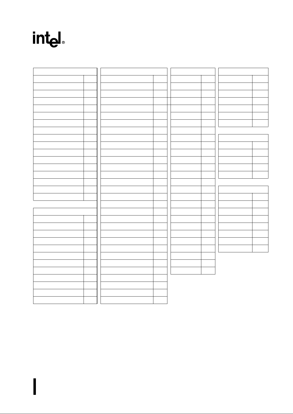
Table 3. Pin Assignment Arranged by Functional Categories
Addr & Data Input/Output (Cont’d) Program Control Processor Control
Name Pin Name Pin Name Pin Name Pin
AD0 22 P2.1 / RXD 28
AINC# 30 EA# 24
AD1 21 P2.2 29 CPVER 31
EXTINT 29
AD2 20
P2.4 30 PACT# 32 PLLEN 6
AD3 19
P2.6 31 PALE# 28 RESET# 23
AD4 18
P2.7 32 PBUS.0 22 XTAL1 52
AD5 17 P3.0 22 PBUS.1 21
XTAL2 51
AD6 16
P3.1 21 PBUS.2 20
AD7 15 P3.2 20 PBUS.3 19 Bus Cont & Status
AD8 14 P3.3 19 PBUS. 4 18
Name Pin
AD9 13 P3.4 18 PBUS. 5 17
ADV# / ALE 2
AD10 12 P3.5 17 PBUS.6 16
CLKOUT 32
AD11 11 P3.6 16 PBUS.7
15 RD# 5
AD12 10 P3.7 15 PBUS.8
14 WR# / WRL# 6
AD13 9 P 4.0 14 PBUS.9
13
AD14 8 P4.1 13 PBUS.10 12 Power & Ground
AD15 7 P4.2 12 PBUS.11
11 Name Pin
P4.3 11 PBUS.12
10 ANGND 39
Input/Output P4.4 10 PBUS.13 9
V
CC
26
Name Pin P4.5 9 PBUS.14 8
V
PP
4
P0.2 / ACH2 33 P4.6 8 PBUS.15 7
V
REF
40
P0.3 / ACH3 34 P4.7 7 PMODE.0 35
VSS 3
P0.4 / ACH4 35
P5.0 2 PMODE.1 36 V
SS1
1
P0.5 / ACH5 36
P5.2 6 PMODE.2 37 V
SS1
25
P0.6 / ACH6 37
P5.3 5 PMODE.3 38
P0.7 / ACH7 38 P6.0 / EPA8 / CO MP0 45 PROG# 29
P1.0 / EPA0 / T2CLK 44 P6.1 / EPA9 / C OMP 1 46 PVER 27
P1.1 / EPA1 43 P6.4 / SC0 47
P1.2 / EPA2 / T2DIR 42 P6.5 / SD0 48
P1.3 / EPA3 41 P6.6 / SC1 49
P2.0 / TXD 27 P6.7 / SD1 50
 Loading...