


*Other brands and names are the property of their respective owners.
Information in this document is provided in connection with Intel products. Intel assumes no liability whatsoever, including infringement of any patent or
copyright, for sale and use of Intel products except as provided in Intel’s Terms and Conditions of Sale for such products. Intel retains the right to make
changes to these specifications at any time, without notice. Microcomputer Products may have minor variations to this specification known as errata.
January 1995COPYRIGHT©INTEL CORPORATION, 1995 Order Number: 272168-002
87C196KD
16-BIT HIGH PERFORMANCE CHMOS
MICROCONTROLLER
Automotive
Y
b
40§Ctoa125§C
Y
32 Kbytes of On-Chip EPROM
Y
232 Byte Register File
Y
768 Bytes of Additional RAM
Y
Register-to-Register Architecture
Y
28 Interrupt Sources/16 Vectors
Y
Peripheral Transaction Server
Y
1.75 ms 16 x 16 Multiply (16 MHz)
Y
3.0 ms 32/16 Divide (16 MHz)
Y
Powerdown and Idle Modes
Y
Five 8-Bit I/O Ports
Y
16-Bit Watchdog Timer
Y
Dynamically Configurable 8-Bit or
16-Bit Buswidth
Y
Full Duplex Serial Port
Y
High Speed I/O Subsystem
Y
16-Bit Timer
Y
16-Bit Up/Down Counter with Capture
Y
3 Pulse-Width-Modulated Outputs
Y
Four 16-Bit Software Timers
Y
8- or 10-Bit 8-Channel A/D Converter
with Sample/Hold
Y
HOLD/HLDA Bus Protocol
Y
OTP One-Time Programmable and
QROM Versions
Y
Available in 12 MHz and 16 MHz
Versions
Y
16 MHz Operation
The 87C196KD 16-bit microcontroller is a high-performance member of the MCSÉ96 microcontroller family.
The 87C196KD is an enhanced 8XC196KC device with 1000 bytes RAM, 16 MHz operation and 32 Kbytes of
on-chip EPROM. Intel’s CHMOS process provides a high-performance processor along with low power consumption.
Four high-speed capture inputs are provided to record times when events occur. Six high-speed outputs are
available for pulse or waveform generation. The high-speed output can also generate four software timers or
start an A/D conversion. Events can be based on the timer or up/down counter.
NOTICE:
This datasheet contains information on products in full production. Specifications within this datasheet
are subject to change without notice. Verify with your local Intel sales office that you have the latest
datasheet before finalizing a design.
MCSÉ96 is a registered trademark of Intel Corporation.
AUTOMOTIVE 87C196KD
272168– 1
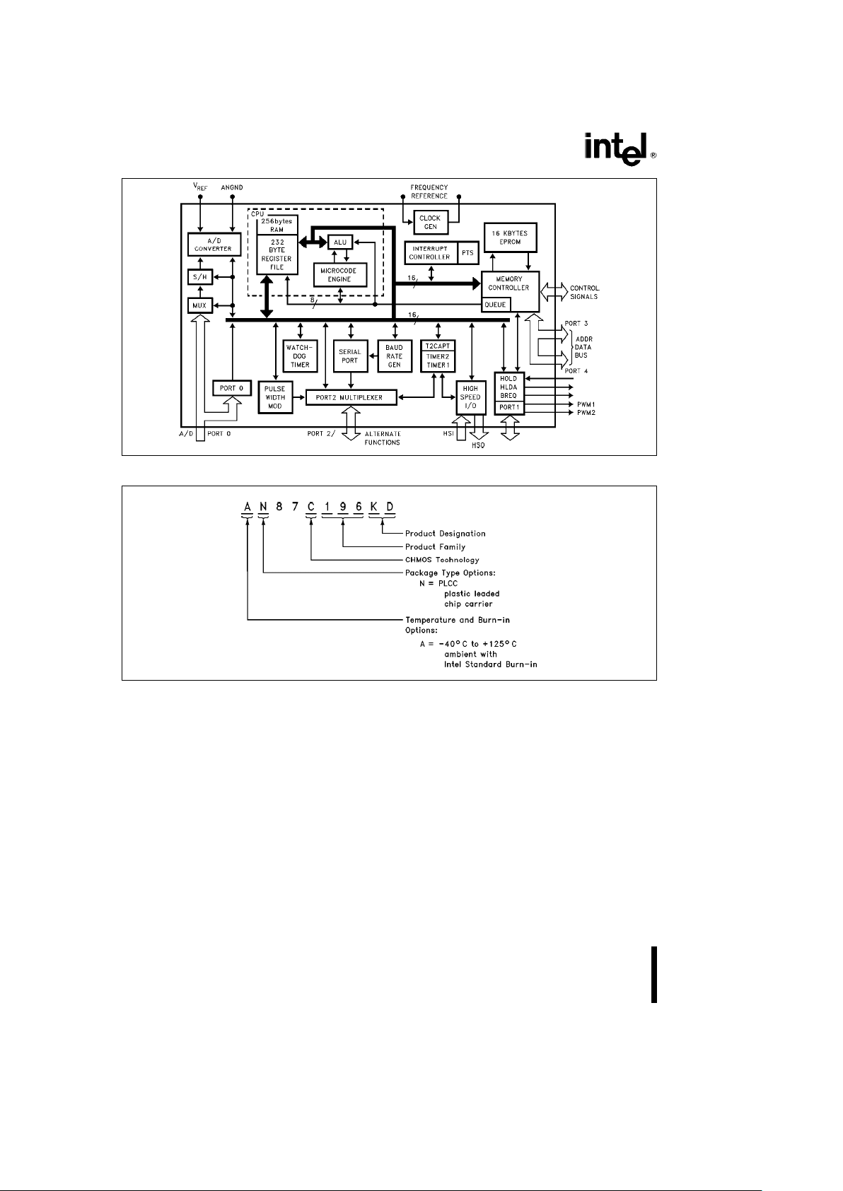
Figure 1. 87C196KD Block Diagram
272168– 2
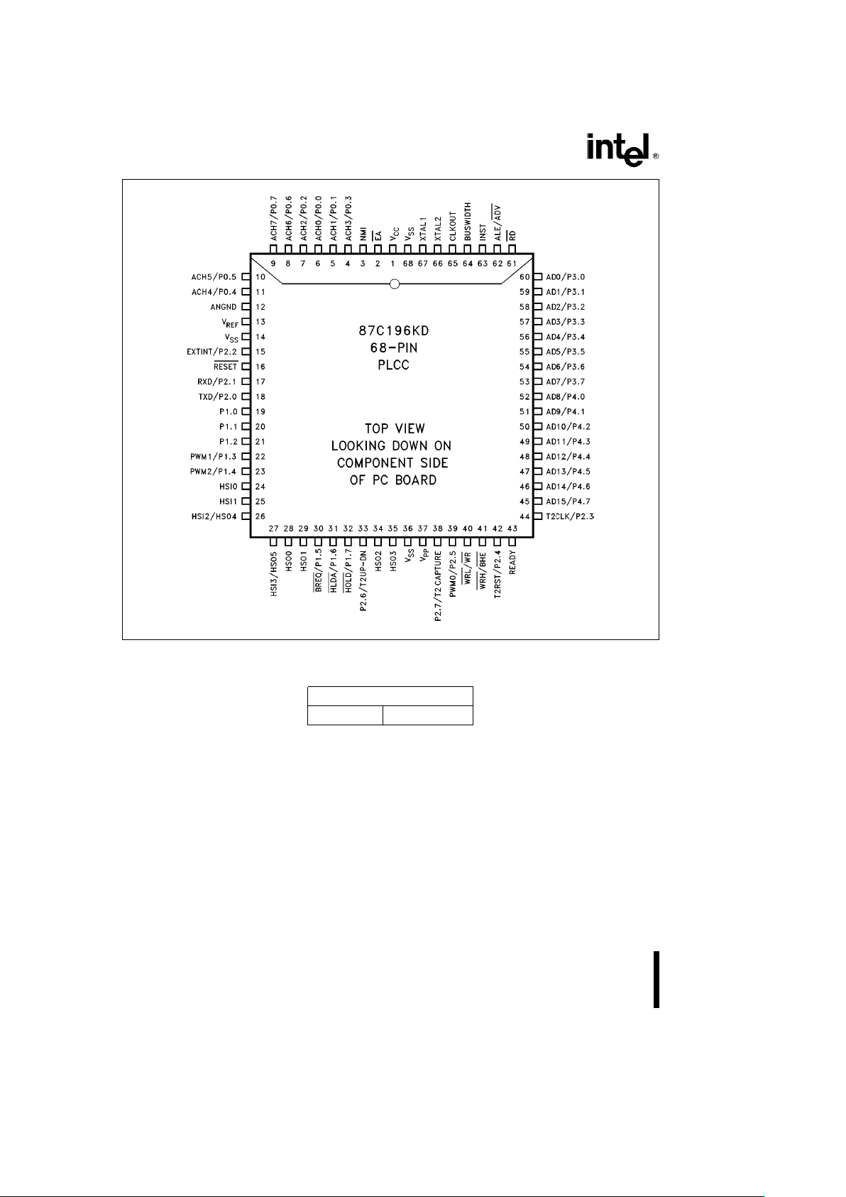
Figure 2. The 87C196KD Family Nomenclature
87C196KD Enhanced Feature Set over the 87C196KC
1. The 87C196KD has twice the RAM and twice the EPROM of the 87C196KC.
2. The vertical windowing scheme has been extended to allow all 1000 bytes of register RAM to be windowed
into the lower register file.
3. A CLKOUT disable bit has been added to the IOC3 SFR. This can be used to reduce noise in systems not
requiring the CLKOUT signal.
2

AUTOMOTIVE 87C196KD
PACKAGING
PLCC Description PLCC Description PLCC Description
9 ACH7/P0.7 54 AD6/P3.6 31 P1.6/HLDA
8 ACH6/P0.6 53 AD7/P3.7 30 P1.5/BREQ
7 ACH2/P0.2 52 AD8/P4.0 29 HSO.1
6 ACH0/P0.0 51 AD9/P4.1 28 HSO.0
5 ACH1/P0.1 50 AD10/P4.2 27 HSO.5/HSI.3
4 ACH3/P0.3 49 AD11/P4.3 26 HSO.4/HSI.2
3 NMI 48 AD12/P4.4 25 HSI.1
2EA 47 AD13/P4.5 24 HSI.0
1V
CC
46 AD14/P4.6 23 P1.4/PWM2
68 V
SS
45 AD15/P4.7 22 P1.3/PWM1
67 XTAL1 44 T2CLK/P2.3 21 P1.2
66 XTAL2 43 READY 20 P1.1
65 CLKOUT 42 T2RST/P2.4 19 P1.0
64 BUSWIDTH 41 BHE
/WRH 18 TXD/P2.0
63 INST 40 WR
/WRL
17 RXD/P2.1
62 ALE/ADV
39 PWM0/P2.5 16 RESET
61 RD 38 P2.7/T2CAPTURE 15 EXTINT/P2.2
60 AD0/P3.0 37 V
PP
14 V
SS
59 AD1/P3.1 36 V
SS
13 V
REF
58 AD2/P3.2 35 HSO.3 12 ANGND
57 AD3/P3.3 34 HSO.2 11 ACH4/P.04
56 AD4/P3.4 33 P2.6/T2UP-DN 10 ACH5/P.05
55 AD5/P3.5 32 P1.7/HOLD
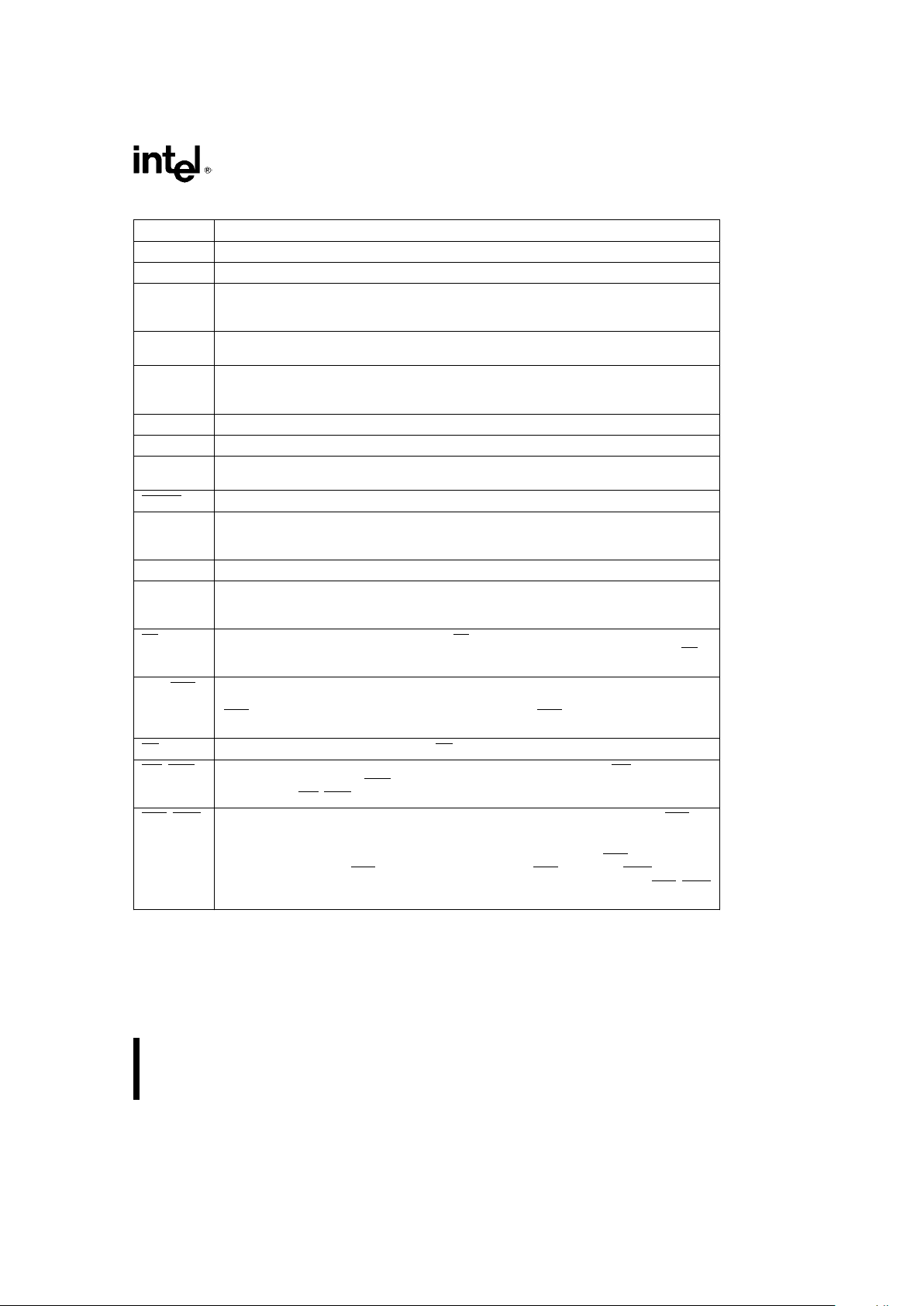
Figure 3. 68-Pin PLCC Functional Pin-out
3
AUTOMOTIVE 87C196KD
272168– 3
Figure 4. 68-Pin PLCC Package
Table 1. Prefix Identification
PLCC
87C196KD AN87C196KD*
*OTP Version
4
AUTOMOTIVE 87C196KD
PIN DESCRIPTIONS
Symbol Name and Function
V
CC
Main supply voltage (5V).
V
SS
Digital circuit ground (0V). There are three VSSpins, all of which must be connected.
V
REF
Reference voltage for the A/D converter (5V). V
REF
is also the supply voltage to the analog
portion of the A/D converter and the logic used to read Port 0. Must be connected for A/D
and Port 0 to function.
ANGND Reference ground for the A/D converter. Must be held at nominally the same potential as
V
SS
.
V
PP
Timing pin for the return from powerdown circuit. Connect this pin with a 1 mF capacitor to
V
SS
anda1MXresistor to VCC. If this function is not used VPPmay be tied to VCC. This pin
is the programming voltage on the EPROM device.
XTAL1 Input of the oscillator inverter and of the internal clock generator.
XTAL2 Output of the oscillator inverter.
CLKOUT Output of the internal clock generator. The frequency of CLKOUT is (/2 the oscillator
frequency.
RESET Reset input to the chip.
BUSWIDTH Input for buswidth selection. If CCR bit 1 is a one, this pin selects the bus width for the bus
cycle in progress. If BUSWIDTH is a 1, a 16-bit bus cycle occurs. If BUSWIDTH isa0an
8-bit cycle occurs. If CCR bit 1 is a 0, the bus is always an 8-bit bus.
NMI A positive transition causes a vector through 203EH.
INST Output high during an external memory read indicates the read is an instruction fetch. INST
is valid throughout the bus cycle. INST is activated only during external memory accesses
and output low for a data fetch.
EA Input for memory select (External Access). EA equal to a TTL-high causes memory
accesses to locations 2000H through 5FFFH to be directed to on-chip ROM/EPROM. EA
equal to a TTL-low causes accesses to those locations to be directed to off-chip memory.
ALE/ADV Address Latch Enable or Address Valid output, as selected by CCR. Both pin options
provide a signal to demultiplex the address from the address/data bus. When the pin is
ADV
, it goes inactive high at the end of the bus cycle. ALE/ADV is activated only during
external memory accesses.
RD Read signal output to external memory. RD is activated only during external memory reads.
WR/WRL Write and Write Low output to external memory, as selected by the CCR. WR will go low for
every external write, while WRL
will go low only for external writes where an even byte is
being written. WR
/WRL is activated only during external memory writes.
BHE/WRH Bus High Enable or Write High output to external memory, as selected by the CCR. BHE
e
0 selects the bank of memory that is connected to the high byte of the data bus. A0e0
selects the bank of memory that is connected to the low byte of the data bus. Thus
accesses to a 16-bit wide memory can be to the low byte only (A0
e
0, BHEe1), to the
high byte only (A0e1, BHEe0), or both bytes (A0e0, BHEe0). If the WRH function is
selected, the pin will go low if the bus cycle is writing to an odd memory location. BHE
/WRH
is valid only during 16-bit external memory write cycles.
5
AUTOMOTIVE 87C196KD
PIN DESCRIPTIONS (Continued)
Symbol Name and Function
READY Ready input to lengthen external memory cycles, for interfacing to slow or dynamic memory,
or for bus sharing. When the external memory is not being used, READY has no effect.
HSI Inputs to High Speed Input Unit. Four HSI pins are available: HSI.0, HSI.1, HSI.2 and HSI.3.
Two of them (HSI.2 and HSI.3) are shared with the HSO Unit.
HSO Outputs from High Speed Output Unit. Six HSO pins are available: HSO.0, HSO.1, HSO.2,
HSI.3, HSO.4 and HSO.5. Two of them (HSO.4 and HSO.5) are shared with the HSI Unit.
Port 0 8-bit high impedance input-only port. These pins can be used as digital inputs and/or as
analog inputs to the on-chip A/D converter.
Port 1 8-bit quasi-bidirectional I/O port.
Port 2 8-bit multi-functional port. All of its pins are shared with other functions in the 87C196KD.
Ports 3 and 4 8-bit bidirectional I/O ports with open drain outputs. These pins are shared with the
multiplexed address/data bus.
HOLD Bus Hold input requesting control of the bus.
HLDA Bus Hold acknowledge output indicating release of the bus.
BREQ Bus Request output activated when the bus controller has a pending external memory
cycle.
6
AUTOMOTIVE 87C196KD
ELECTRICAL CHARACTERISTICS
Absolute Maximum Ratings*
Ambient Temperature
Under Bias ААААААААААААААААА
b
40§Ctoa125§C
Storage Temperature ААААААААААb65§Ctoa150§C
Voltage On Any Pin to V
SS
Except EA and VPPААААААААААААb0.5V toa7.0V
Voltage from EA or
V
PP
to VSSААААААААААААААААААb0.5V toa13.0V
Power Dissipation АААААААААААААААААААААААА0.43W
NOTICE: This is a production data sheet. The specifications are subject to change without notice.
*
WARNING: Stressing the device beyond the ‘‘Absolute
Maximum Ratings’’ may cause permanent damage.
These are stress ratings only. Operation beyond the
‘‘Operating Conditions’’ is not recommended and extended exposure beyond the ‘‘Operating Conditions’’
may affect device reliability.
OPERATING CONDITIONS
Symbol Description Min Max Units
T
A
Ambient Temperature Under Bias
b
40
a
125
§
C
V
CC
Digital Supply Voltage 4.50 5.50 V
V
REF
Analog Supply Voltage 4.50 5.50 V
F
OSC
Oscillator Frequency 4 16 MHz
NOTE:
ANGND and V
SS
should be nominally at the same potential.
DC CHARACTERISTICS (Over Specified Operating Conditions)
Symbol Description Min Max Units Test Conditions
V
IL
Input Low Voltage
b
0.5 0.8 V
V
IH
Input High Voltage (Note 1) 0.2 V
CC
a
1.0 V
CC
a
0.5 V
V
IH1
Input High Voltage on XTAL 1, EA 0.7 V
CC
V
CC
a
0.5 V
V
IH2
Input High Voltage on RESET 2.2 V
CC
a
0.5 V
V
OL
Output Low Voltage 0.3 V I
OL
e
200 mA
0.45 V I
OL
e
2.8 mA
1.5 V I
OL
e
7mA
V
OL1
Output Low Voltage 0.8 V I
OL
ea
0.2 mA
in RESET on P2.5 (Note 2)
V
OH
Output High Voltage V
CC
b
0.3 V I
OH
eb
200 mA
(Standard Outputs) V
CC
b
0.7 V I
OH
eb
3.2 mA
V
CC
b
1.5 V I
OH
eb
7mA
V
OH1
Output High Voltage V
CC
b
0.3 V I
OH
eb
10 mA
(Quasi-bidirectional Outputs) V
CC
b
0.7 V I
OH
eb
30 mA
V
CC
b
1.5 V I
OH
eb
60 mA
I
OH2
Output High Current
b
0.8 mA V
IH
e
V
CC
b
1.5 V
In RESET on P2.0 (Note 2)
NOTES:
1. All pins except RESET, XTAL1 and EA.
2. Violating these specifications in Reset may cause the part to enter test modes.
7

AUTOMOTIVE 87C196KD
DC CHARACTERISTICS (Over Specified Operating Conditions)
Symbol Description Min Typ Max Units Test Conditions
I
LI
Input Leakage Current (Std. Inputs)
g
10 mA0kV
IN
k
V
CC
b
0.3V
I
LI1
Input Leakage Current (Port 0)
g
3 mA0kV
IN
k
V
REF
I
TL
1 to 0 Transition Current (QBD Pins)
b
650 mAV
IN
e
2.0V
I
IL
Logical 0 Input Current (QBD Pins)
b
70 mAV
IN
e
0.45V
I
CC
Active Mode Current in Reset 65 75 mA XTAL1e16 MHz
I
REF
A/D Converter Reference Current 2 5 mA
V
CC
e
V
PP
e
V
REF
e
5.5V
I
IDLE
Idle Mode Current 15 30 mA
R
RST
Reset Pullup Resistor 6K 65K X V
CC
e
5.0V, V
IN
e
4.0V
C
S
Pin Capacitance (Any Pin to VSS)10pF
NOTES:
(Notes apply to all specifications)
1. QBD (Quasi-bidirectional) pins include Port 1, P2.6 and P2.7.
2. Standard Outputs include AD0 – 15, RD
,WR, ALE, BHE, INST, HSO pins, PWM/P2.5, CLKOUT, RESET, Ports 3 and 4,
TXD/P2.0 and RXD (in serial mode 0). The V
OH
specification is not valid for RESET. Ports 3 and 4 are open-drain outputs.
3. Standard Inputs include HSI pins, READY, BUSWIDTH, NMI, RXD/P2.1, EXTINT/P2.2, T2CLK/P2.3 and T2RST/P2.4.
4. Maximum current per pin must be externally limited to the following values if V
OL
is held above 0.45V or VOHis held
below V
CC
b
0.7V:
I
OL
on Output pins: 10 mA
I
OH
on quasi-bidirectional pins: self limiting
I
OH
on Standard Output pins: 10 mA
5. Maximum current per bus pin (data and control) during normal operation is
g
3.2 mA.
6. During normal (non-transient) conditions the following total current limits apply:
Port 1, P2.6 I
OL
:29mA IOHis self limiting
HSO, P2.0, RXD, RESET
IOL:29mA IOH:26mA
P2.5, P2.7, WR
, BHE IOL:13mA IOH:11mA
AD0–AD15 I
OL
:52mA IOH:52mA
RD
, ALE, INST – CLKOUT IOL:13mA IOH:13mA
8

AUTOMOTIVE 87C196KD
ICCMAXe3.88cFreqa8.43
I
IDLE
MAXe1.65cFreqa2.2 272168– 4
Figure 5. ICCand I
IDLE
vs Frequency
AC CHARACTERISTICS
For use over specified operating conditions.
Test Conditions: Capacitive load on all pinse100 pF, Rise and fall timese10 ns, F
OSC
e
16 MHz
The system must meet these specifications to work with the 87C196KD:
Symbol Description Min Max Units Notes
T
AVYV
Address Valid to READY Setup 2 T
OSC
b
75 ns
T
LLYV
ALE Low to READY Setup T
OSC
b
77 ns
T
YLYH
Non READY Time No upper limit ns
T
CLYX
READY Hold after CLKOUT Low 0 T
OSC
b
30 ns (Note 1)
T
LLYX
READY Hold after ALE Low T
OSC
b
15 2 T
OSC
b
40 ns (Note 1)
T
AVGV
Address Valid to Buswidth Setup 2 T
OSC
b
75 ns
T
LLGV
ALE Low to Buswidth Setup T
OSC
b
65 ns
T
CLGX
Buswidth Hold after CLKOUT Low 0 ns
T
AVDV
Address Valid to Input Data Valid 3 T
OSC
b
55 ns (Note 2)
T
RLDV
RD Active to Input Data Valid T
OSC
b
25 ns (Note 2)
T
CLDV
CLKOUT Low to Input Data Valid T
OSC
b
45 ns
T
RHDZ
End of RD to Input Data Float T
OSC
ns
T
RXDX
Data Hold after RD Inactive 0 ns
NOTES:
1. If max is exceeded, additional wait states will occur.
2. If wait states are used, add 2 T
OSC
* N, where Nenumber of wait states.
9

AUTOMOTIVE 87C196KD
AC CHARACTERISTICS (Continued)
For use over specified operating conditions.
Test Conditions: Capacitive load on all pins
e
100 pF, Rise and fall timese10 ns, F
OSC
e
16 MHz
The 87C196KD will meet these specifications:
Symbol Description Min Max Units Notes
F
XTAL
Frequency on XTAL
1
4.0 16 MHz (Note 1)
T
OSC
I/F
XTAL
62.5 250 ns
T
XHCH
XTAL1 High to CLKOUT High or Low 20 110 ns
T
CLCL
CLKOUT Cycle Time 2 T
OSC
ns
T
CHCL
CLKOUT High Period T
OSC
b
10 T
OSC
a
15 ns
T
CLLH
CLKOUT Falling Edge to ALE Rising
b
515ns
T
LLCH
ALE Falling Edge to CLKOUT Rising
b
25
a
15 ns
T
LHLH
ALE Cycle Time 4 T
OSC
ns (Note 4)
T
LHLL
ALE High Period T
OSC
b
10 T
OSC
a
10 ns
T
AVLL
Address Setup to ALE Falling Edge T
OSC
b
15
T
LLAX
Address Hold after ALE Falling Edge T
OSC
b
35 ns
T
LLRL
ALE Falling Edge to RD Falling Edge T
OSC
b
35 ns
T
RLCL
RD Low to CLKOUT Falling Edge 0 35 ns
T
RLRH
RD Low Period T
OSC
b
5 ns (Note 4)
T
RHLH
RD Rising Edge to ALE Rising Edge T
OSC
T
OSC
a
25 ns (Note 2)
T
RLAZ
RD Low to Address Float 5 ns
T
LLWL
ALE Falling Edge to WR Falling Edge T
OSC
b
10 ns
T
CLWL
CLKOUT Low to WR Falling Edge 0 25 ns
T
QVWH
Data Stable to WR Rising Edge T
OSC
b
30 (Note 4)
T
CHWH
CLKOUT High to WR Rising Edge
b
515ns
T
WLWH
WR Low Period T
OSC
b
30 ns (Note 4)
T
WHQX
Data Hold after WR Rising Edge T
OSC
b
25 ns
T
WHLH
WR Rising Edge to ALE Rising Edge T
OSC
b
10 T
OSC
a
15 ns (Note 2)
T
WHBX
BHE, INST after WR Rising Edge T
OSC
b
10 ns
T
WHAX
AD8–15 HOLD after WR Rising T
OSC
b
30 ns (Note 3)
T
RHBX
BHE, INST after RD Rising Edge T
OSC
b
10 ns
T
RHAX
AD8–15 HOLD after RD Rising T
OSC
b
25 ns (Note 3)
NOTES:
1. Testing performed at 4.0 MHz. However, the device is static by design and will typically operate below 1 Hz.
2. Assuming back-to-back bus cycles.
3. 8-Bit bus only.
4. If wait states are used, add 2 T
OSC
* N, where Nenumber of wait states.
10

AUTOMOTIVE 87C196KD
System Bus Timings
272168– 5
11

AUTOMOTIVE 87C196KD
READY Timings (One Wait State)
272168– 6
Buswidth Timings
272168– 7
12

AUTOMOTIVE 87C196KD
HOLD/HLDA Timings
Symbol Description Min Max Units Notes
T
HVCH
HOLD Setup 60 ns (Note 1)
T
CLHAL
CLKOUT Low to HLDA Low
b
15 15 ns
T
CLBRL
CLKOUT Low to BREQ Low
b
15 15 ns
T
HALAZ
HLDA Low to Address Float 15 ns
T
HALBZ
HLDA Low to BHE, INST, RD,WRWeakly Driven 20 ns
T
CLHAH
CLKOUT Low to HLDA High
b
15 15 ns
T
CLBRH
CLKOUT Low to BREQ High
b
15 15 ns
T
HAHAX
HLDA High to Address No Longer Float
b
15 ns
T
HAHBV
HLDA High to BHE, INST, RD, WR Valid
b
10 15 ns
T
CLLH
CLKOUT Low to ALE High
b
515 ns
NOTE:
1. To guarantee recognition at next clock.
DC SPECIFICATIONS IN HOLD
Min Max Units
Weak Pullups on ADV, RD, 50K 250K V
CC
e
5.5V, V
IN
e
0.45V
WR
,WRL, BHE
Weak Pulldowns on
10K 50K V
CC
e
5.5V, V
IN
e
2.4
ALE, INST
272168– 8
13

AUTOMOTIVE 87C196KD
EXTERNAL CLOCK DRIVE
Symbol Parameter Min Max Units
1/T
XLXL
Oscillator Frequency 4.0 16.0 MHz
T
XLXL
Oscillator Frequency 62.5 250 ns
T
XHXX
High Time 22 ns
T
XLXX
Low Time 22 ns
T
XLXH
Rise Time 10 ns
T
XHXL
Fall Time 10 ns
EXTERNAL CLOCK DRIVE WAVEFORMS
272168– 9
An external oscillator may encounter as much as a 100 pF load at XTAL1 when it starts-up. This is due to
interaction between the amplifier and its feedback capacitance. Once the external signal meets the V
IL
and
V
IH
specifications the capacitance will not exceed 20 pF.
AC TESTING INPUT, OUTPUT WAVEFORMS
272168– 10
AC Testing inputs are driven at 2.4V for a Logic ‘‘1’’ and 0.45V for
a Logic ‘‘0’’ Timing measurements are made at 2.0V for a Logic
‘‘1’’ and 0.8V for a Logic ‘‘0’’.
FLOAT WAVEFORMS
272168– 11
For timing purposes a port pin is no longer floating when a
100 mV change from load voltage occurs and begins to float
when a 100 mV change from the loaded V
OH/VOL
level occurs
I
OL/IOH
e
g
15 mA.
EXPLANATION OF AC SYMBOLS
Each symbol is two pairs of letters prefixed by ‘‘T’’ for time. The characters in a pair indicate a signal and its
condition, respectively. Symbols represent the time between the two signal/condition points.
Conditions:
HÐ High
LÐ Low
VÐ Valid
XÐ No Longer Valid
ZÐ Floating
Signals:
AÐ Address
BÐ BHE
CÐ CLKOUT
DÐ DATA
GÐ Buswidth
HÐ HOLD
HAÐ HLDA
LÐ ALE/ADV
BRÐ BREQ
RÐ RD
WÐ WR/WRH/WRL
XÐ XTAL1
YÐ READY
QÐ Data Out
14

AUTOMOTIVE 87C196KD
AC CHARACTERISTICSÐSERIAL PORTÐSHIFT REGISTER MODE
SERIAL PORT TIMINGÐSHIFT REGISTER MODE
Symbol Parameter Min Max Units
T
XLXL
Serial Port Clock Period (BRRt8002H) 6 T
OSC
ns
T
XLXH
Serial Port Clock Falling Edge 4 T
OSC
b
50 4 T
OSC
a
50 ns
to Rising Edge (BRR
t
8002H)
T
XLXL
Serial Port Clock Period (BRRe8001H) 4 T
OSC
ns
T
XLXH
Serial Port Clock Falling Edge 2 T
OSC
b
50 2 T
OSC
a
50 ns
to Rising Edge (BRR
e
8001H)
T
QVXH
Output Data Setup to Clock Rising Edge 2 T
OSC
b
50 ns
T
XHQX
Output Data Hold after Clock Rising Edge 2 T
OSC
b
50 ns
T
XHQV
Next Output Data Valid after Clock Rising Edge 2 T
OSC
a
50 ns
T
DVXH
Input Data Setup to Clock Rising Edge T
OSC
a
50 ns
T
XHDX
Input Data Hold after Clock Rising Edge 0 ns
T
XHQZ
Last Clock Rising to Output Float 1 T
OSC
ns
WAVEFORMÐSERIAL PORTÐSHIFT REGISTER MODE
SERIAL PORT WAVEFORMÐSHIFT REGISTER MODE
272168– 12
15

AUTOMOTIVE 87C196KD
EPROM SPECIFICATIONS
AC EPROM Programming Characteristics
Operating Conditions: Load Capacitancee150 pF, T
A
ea
25§Cg5§C, VCC,V
REF
e
5V,
V
SS
, ANGNDe0V, V
PP
e
12.50Vg0.25V, EAe12.50Vg0.25V
Symbol Description Min Max Units
T
SHLL
Reset High to First PALE Low 1100 T
OSC
T
LLLH
PALE Pulse Width 50 T
OSC
T
AVLL
Address Setup Time 0 T
OSC
T
LLAX
Address Hold Time 100 T
OSC
T
PLDV
PROG Low to Word Dump Valid 50 T
OSC
T
PHDX
Word Dump Data Hold 50 T
OSC
T
DVPL
Data Setup Time 0 T
OSC
T
PLDX
Data Hold Time 400 T
OSC
T
PLPH
(2) PROG Pulse Width 50 T
OSC
T
PHLL
PROG High to Next PALE Low 220 T
OSC
T
LHPL
PALE High to PROG Low 220 T
OSC
T
PHPL
PROG High to Next PROG Low 220 T
OSC
T
PHIL
PROG High to AINC Low 0 T
OSC
T
ILIH
AINC Pulse Width 240 T
OSC
T
ILVH
PVER Hold after AINC Low 50 T
OSC
T
ILPL
AINC Low to PROG Low 170 T
OSC
T
PHVL
PROG High to PVER Valid 220 T
OSC
NOTES:
1. Run Time Programming is done with F
OSC
e
6.0 MHz to 12.0 MHz, V
REF
e
5Vg0.50V. T
A
ea
25§Ctog5§C and
V
PP
e
12.50V. For run-time programming over a full operating range, contact the factory.
2. This specification is for the Word Dump Mode. For programming pulses, use 300 T
OSC
a
100 ms.
DC EPROM Programming Characteristics
Symbol Description Min Max Units
I
PP
VPPSupply Current (When Programming) 100 mA
NOTE:
V
PP
must be within 1V of VCCwhile V
CC
k
4.5V. VPPmust not have a low impedance path to ground of VSSwhile
V
CC
l
4.5V.
16

AUTOMOTIVE 87C196KD
EPROM PROGRAMMING WAVEFORMS
SLAVE PROGRAMMING MODE DATA PROGRAM MODE WITH SINGLE PROGRAM PULSE
272168– 13
SLAVE PROGRAMMING MODE IN WORD DUMP WITH AUTO INCREMENT
272168– 14
17

AUTOMOTIVE 87C196KD
SLAVE PROGRAMMING MODE TIMING IN DATA PROGRAM WITH REPEATED PROG PULSE AND
AUTO INCREMENT
272168– 15
18

AUTOMOTIVE 87C196KD
10-BIT A/D CHARACTERISTICS
The speed of the A/D converter in the 10-bit mode
can be adjusted by setting a clock prescaler on or
off. At high frequencies more time is needed for the
comparator to settle. The maximum frequency with
the clock prescaler disabled is 6 MHz. The conversion times with the prescaler turned on or off is
shown in the table below. The ADÐTIME register
has not been characterized for the 10-bit mode.
The converter is ratiometric, so the absolute accuracy is dependent on the accuracy and stability
of V
REF.VREF
must be close to VCCsince it supplies
both the resistor ladder and the digital section of the
converter.
A/D CONVERTER SPECIFICATIONS
The specifications given below assume adherence
to the Operating Conditions section of this datasheet. Testing is performed with V
REF
e
5.12V.
Clock Prescaler On Clock Prescaler Off
IOC2.4
e
0 IOC2.4e1
156.5 States 89.5 States
19.5 ms
@
16 MHz 29.8 ms@6 MHz
Parameter Typical
(3)
Minimum Maximum Units* Notes
Resolution 1024 1024 Levels
10 10 Bits
Absolute Error 0
g
4 LSBs
Full Scale Error
g
3 LSBs
Zero Offset Error
g
3 LSBs
Non-Linearity 0
g
4 LSBs
Differential Non-Linearity Error
l
b
1
a
2 LSBs
Channel-to-Channel Matching 0
g
1 LSBs
Repeatability
g
0.25 LSBs
Temperature Coefficients:
Offset 0.009 LSB/
§
C
Full Scale 0.009 LSB/
§
C
Differential Non-Linearity 0.009 LSB/
§
C
Off Isolation
b
60 dB 1, 2
Feedthrough
b
60 dB 1
VCCPower Supply Rejection
b
60 dB 1
Input Resistance 750 1.2K X
DC Input Leakage 0 3.0 mA
Sample Time: Prescaler On 16 States
Prescaler Off 8 States
Input Capacitance 3 pF
NOTES:
*An ‘‘LSB’’, as used here, has a value of approximately 5 mV.
1. DC to 100 KHz.
2. Multiplexer Break-Before-Make Guaranteed.
3. Typical values are expected for most devices at 25
§
C.
19

AUTOMOTIVE 87C196KD
8-BIT MODE A/D CHARACTERISTICS
The 8-bit mode trades off resolution for a faster conversion time. The ADÐTIME register must be used
when performing an 8-bit conversion.
The following specifications are tested
@
16 MHz
with OA6H in ADÐTIME. The actual ADÐTIME register is tested with all possible values, to ensure
functionality, but the accuracy of the A/D converter
is not.
Sample Time Convert Time
20 States 56 States
A6H in ADÐTIME
9.8 ms
@
16 MHz
Parameter Typical Minimum Maximum Units* Notes
Resolution 256 256 Levels
8 8 Bits
Absolute Error 0
g
2 LSBs
Full Scale Error
g
1 LSBs
Zero Offset Error
g
2 LSBs
Non-Linearity 0
g
2 LSBs
Differential Non-Linearity Error
l
b
1
a
1 LSBs
Channel-to-Channel Matching
g
1 LSBs
Repeatability
g
0.25 LSBs
Temperature Coefficients:
Offset 0.003 LSB/
§
C
Full Scale 0.003 LSB/
§
C
Differential Non-Linearity 0.003 LSB/
§
C
NOTES:
*An ‘‘LSB’’, as used here, has a value of approximately 20 mV.
1. Typical values are expected for most devices at 25
§
C.
8XC196KB TO 87C196KD DESIGN
CONSIDERATIONS
1. Memory Map. The 87C196KD has 512 bytes of
RAM/SFRs and 32K of ROM/EPROM. The extra
256 bytes of RAM will reside in locations 100H –
1FFH and the extra 24K of EPROM will reside in
locations 4000H –9FFFH. These locations are
external memory on the 87C196KB.
2. The CDE pin on the KB has become a V
SS
pin on
the KC to support 16 MHz operation.
3. EPROM programming. The 87C196KD has a dif-
ferent programming algorithm to support 32K of
on-board memory. When performing Run-Time
Programming, use the section of code on page
99 of the 80C196KC User’s Guide, Order Number 270704.
4. ONCE Mode Entry. The ONCE mode is entered
on the 87C196KD by driving the TXD pin low on
the rising edge of RESET. The TXD pin is held
high by a pullup that is specified at 1.4 mA and
remain at 2.0V. This Pullup must not be overridden or the 87C196KD will enter the ONCE mode.
5. During the bus HOLD state, the 87C196KD weakly holds RD, WR, ALE, BHE and INST in their
inactive states. The 87C196KB only holds ALE in
its inactive state.
6. A RESET pulse from the 87C196KD is 16 states
rather than 4 states as on the 87C196KB (i.e., a
watchdog timer overflow). This provides a longer
RESET pulse for other devices in the system.
20

AUTOMOTIVE 87C196KD
8XC196KD ERRATA
1. It is possible for the device to fail to recognize an
interrupt on EXTINIT, for both P2.2 and P0.7, and
NMI. The problem is most likely to occur on P0.7
while the device is operating at low voltage
(
k
4.7V), high frequency (16 MHz) and high tem-
perature (
l
85§C). There is a window of about
2 ns near clockout falling during which these interrupts may be missed.
2. In Mode 0, the serial port does not work if the
highest baud rate is selected (SPÐBAUD
e
8001h). Data shifted into the device will not be
correctly read at this baud rate.
DATASHEET REVISION HISTORY
The following are the key differences between this
datasheet and the -005 version:
1. The ‘‘preliminary’’ status was dropped and replaced with production status (no label).
Trademarks were updated.
21
 Loading...