

Intel Corporation AN83C196LD-22, AN83C196LD-18, AN83C196LD, AN83C196LC-22, AN83C196LC-18 Datasheet
...
ADVANCE INFORMATION
COPYRIGHT © INTEL CORPORATION, 1996 December 1996 Order Number: 272805-001
83C196LC, 83C196LD
CHMOS 16-BIT MICROCONT R O LLER
Automotive
NOTE
This document contains information on products in the sampling and initial production
phases of development. The specifications are subject to change without notice. Verify
with your local Intel sales office that you have the latest datasheet before finalizing a
design.
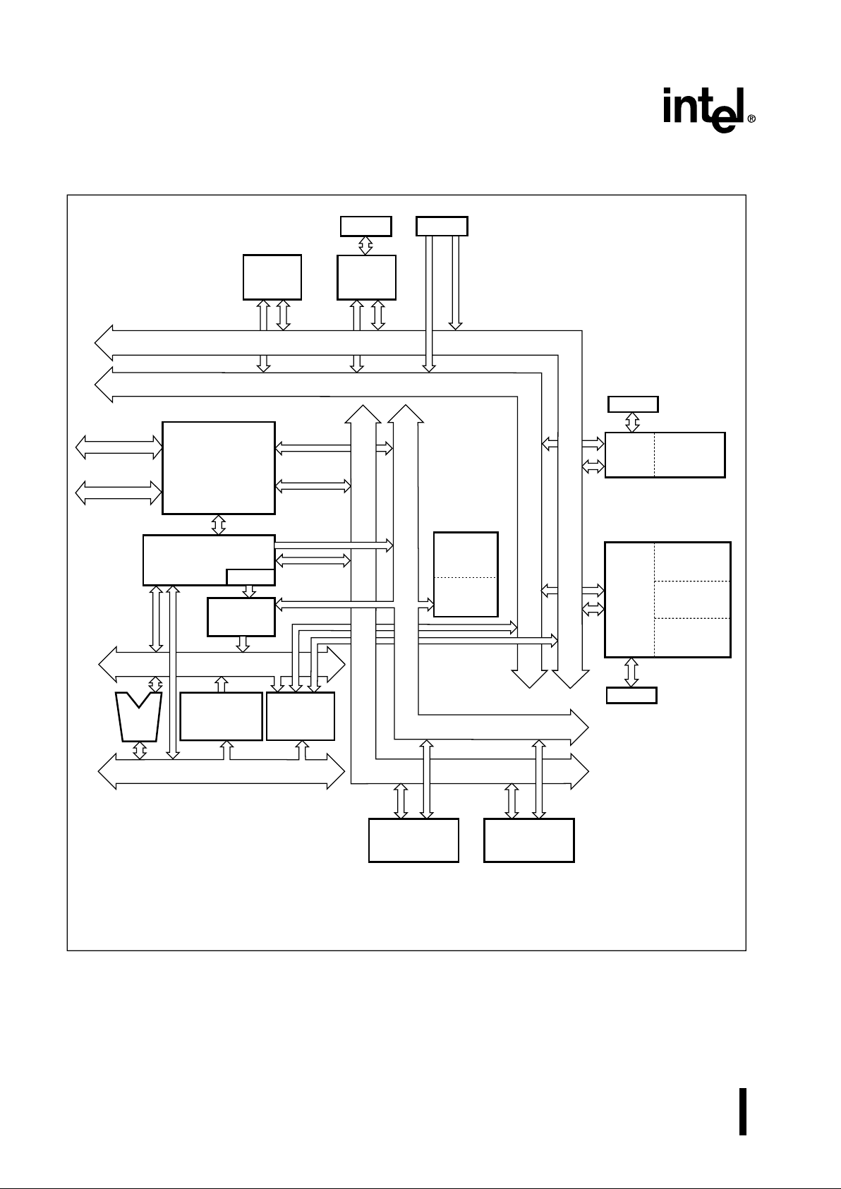
The 83C196LC, 83C196LD are low-cost, pin-compatible replacements for the existing 87C196JT and
87C196JR, respectively. These products feature an enhanced synchronous serial I/O (SSIO) port for more
flexible communication to other devices. The enhanced SSIO is compatible with Motorola’s Serial Peripheral
Interface (SPI) protocol and National’s Microwire protocol. To optimize die size, the A/D converter was
removed for use in those applications that use an off-chip A/D converter.
The MCS
®
96 microcontroller family members are all high-performanc e microcontrollers with 16-bit CPUs.
The 83C196LC, 83C196LD are composed of a high-speed core with the following peripherals: an
asynchronous/synchronous serial I/O port (8096 compatible) with a dedicated 16-bit baud-rate generator; an
additional synchronous serial I/O port with full duplex master/slave transceivers; a flexible timer/counter
structure with prescaler, cascading, and quadrature capabilities; six modularized, multiplexed high-speed I/O
for capture and compare (called event processor array) with 200 ns resolution and double buffered inputs;
and a sophisticated, prioritized interrupt structure with programmable peripheral transaction server (PTS).
The 83C196LC has the highest memory density of the 52-pin MCS 96 microcontroller family, with 32 Kbytes
of on-chip ROM, 1 Kbyte of on-chip register RAM, and 512 bytes of code RAM. The high memory integration
of the 83C196LC supports high functionality in a low pin-count package and the use of the C programming
language.
■ 22 MHz operation
†
■ 32 Kbytes of on-chip ROM (LC)
16 Kbytes of on-chip ROM (LD)
■ 1 Kbyte of on-chip register RAM (LC)
384 bytes of on-chip register RAM (LD)
■ 512 bytes of on-chip code RAM
(LC only)
■ Register-to-register architecture
■ Peripheral transaction server (PTS)
with high-speed, microcoded interrupt
service routines
■ Full-duplex serial I/O port with
dedicated baud-rate generator
■ Enhanced full-duplex, synchronous
serial I/O port (SSIO)
†
12 MHz standard; 18 MHz and 22 MHz are speed
premium
■ High-speed event processor array
—Six capture/compare channels
—Two compare-only channels
— Two 16-bit software timers
■ Programmable 8- or 16-bit external bus
■ Design enhancements for EMI
reduction
■ Oscillator failure detection circuitry
■ SFR register that indicates the source
of the last reset
■ Watchdog timer (WDT)
■ Cost reduced replacements for the
87C196JT and 87C196JR.
■ –40° C to +125° C ambient temperature
■ 52-pin PLCC package
2 ADVANCE INFORMATION
83C196LC, 83C196L D — AUTOMOTIVE
Figure 1. 83C196LC, 83C196LD Block Diagram
Code/Data RAM
512 Bytes
(LC only)
Queue
Source (16)
Destination (16)
AD15:0
EPA
2 Timers
6 Capture/
Compare
Channels †
Bus
Controller
Watchdog
Timer
Enhanced
SSIO
ROM
32 Kbytes (LC)
16 Kbytes (LD)
A3383-01
SIO
Baud-rate
Generator
Port 6
Memory Data Bus (16)
Bus-Control
Interface Unit
Microcode
Engine
Peripheral
Transaction
Server
Memory
Interface
Unit
Register RAM
1 Kbyte (LC)
384 Bytes (LD)
ALU
Interrupt
Controller
Bus Control
Peripheral Addr Bus (10)
Peripheral Data Bus (16)
Memory Addr Bus (16)
2
Compare-only
Channels
Port 2
Port 1,6
† A seventh capture/compare channel (EPA7) is available as a software timer. It is not connected to a package pin.
Port 0
ADVANCE INFORMATION 3
AUTOMOTIVE — 83C196LC, 83C196LD
1.0 NOMENCLATURE OVERVIEW
Figure 2. Product Nomenclature
Table 1. Description of Product Nomenclature
Parameter Options Description
Temperature and Burn-in Options A Automotive operating temperature range (–40° C to
125° C ambient) with Intel standard burn-in.
Packaging Options N PLCC
Program-memory Options 3 Internal ROM
Process Information C CHMOS
Product Family 196L
x
8XC196Lx family of products
Device Speed no mark
18
22
12 MHz
18 MHz
22 MHz
Program Memory Options
XXXXX XXXX8XXX
Packaging Options
Temperature and Burn-in Options
A2815-01
Process Information
Product Family
Device Speed
4 ADVANCE INFORMATION
83C196LC, 83C196L D — AUTOMOTIVE
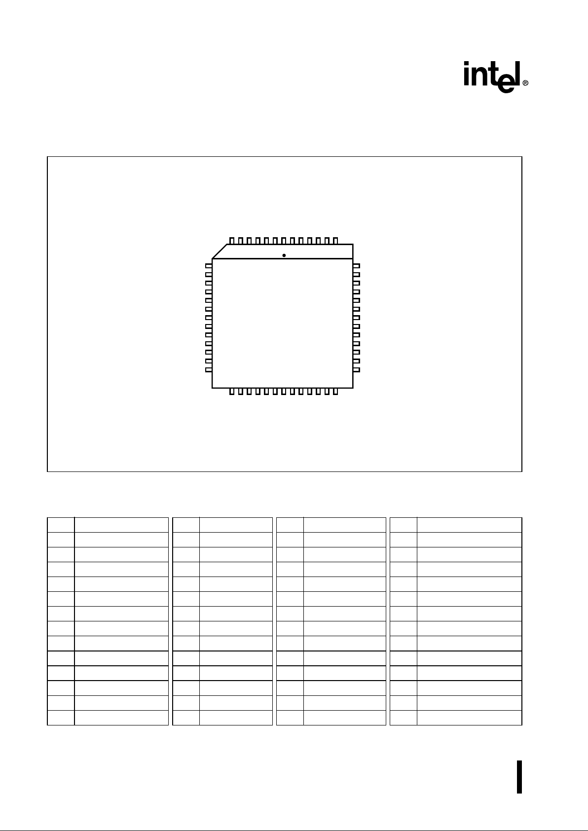
2.0 PINOUT
Figure 3. 83C196LC, 83C196LD 52-pin PLCC Package
Table 2. 83C196LC, 83C196LD 52-pin PLCC Package Pin Assignments
Pin Name Pin Name Pin Name Pin Name
1V
SS
14 AD8/P4.0 27 P2.0/TXD 40 V
CC
2 P5.0/ADV#/ALE 15 AD7/P3.7 28 P2.1/RXD 41 P1.3/EPA3
3V
SS
16 AD6/P3.6 29 P2.2/EXTINT 42 P1.2/EPA2/T2DIR
4V
PP
17 AD5/P3.5 30 P2.4 43 P1.1/EPA1
5 P5.3/RD# 18 AD4/P3.4 31 P2.6/ONCE# 44 P1.0/EPA0/T2CLK
6 P5.2/WR#/WRL# 19 AD3/P3.3 32 P2.7/CLKOUT 45 P6.0/EPA8
7 AD15/P4.7 20 AD2/P3.2 33 P0.2 46 P6.1/EPA9
8 AD14/P4.6 21 AD1/P3.1 34 P0.3 47 P6.4/SC0
9 AD13/P4.5 22 AD0/P3.0 35 P0.4 48 P6.5/SD0
10 AD12/P4.4 23 RESET# 36 P0.5 49 P6.6/SC1
11 AD11/P4.3 24 EA# 37 P0.6 50 P6.7/SD1
12 AD10/P4.2 25 V
SS
38 P0.7 51 XTAL2
13 AD9/P4.1 26 V
CC
39 V
SS
52 XTAL1
P6.1 / EPA9
P6.0 / EPA8
P1.0 / EPA0 / T2CLK
P1.1 / EPA1
P1.2 / EPA2 / T2DIR
P1.3 / EPA3
V
CC
V
SS
P0.7
P0.6
P0.5
P0.4
P0.3
AD15 / P4.7
P5.2 / WR# / WRL#
P5.3 / RD#
V
PP
V
SS
P5.0 / ADV# / ALE
V
SS
XTAL1
XTAL2
P6.7 / SD1
P6.6 / SC1
P6.5 / SD0
P6.4 / SC0
A3403-01
AD14 / P4.6
AD13 / P4.5
AD12 / P4.4
AD11 / P4.3
AD10 / P4.2
AD9 / P4.1
AD8 / P4.0
AD7 / P3.7
AD6 / P3.6
AD5 / P3.5
AD4 / P3.4
AD3 / P3.3
AD2 / P3.2
46
45
44
43
42
41
40
39
38
37
36
35
34
N83C196LC
N83C196LD
View of component as
mounted on PC board
8
9
10
11
12
13
14
15
16
17
18
19
20
AD1 / P3.1
AD0 / P3.0
RESET#
EA#
V
SS
V
CC
P2.0 / TXD
P2.1 / RXD
P2.2 / EXTINT
P2.4
P2.6 / ONCE#
P2.7 / CLKOUT
P0.2
21
22
23
24
25
26
27
28
29
30
31
32
33
7654321
52
51
50
49
48
47
ADVANCE INFORMATION 5
AUTOMOTIVE — 83C196LC, 83C196LD
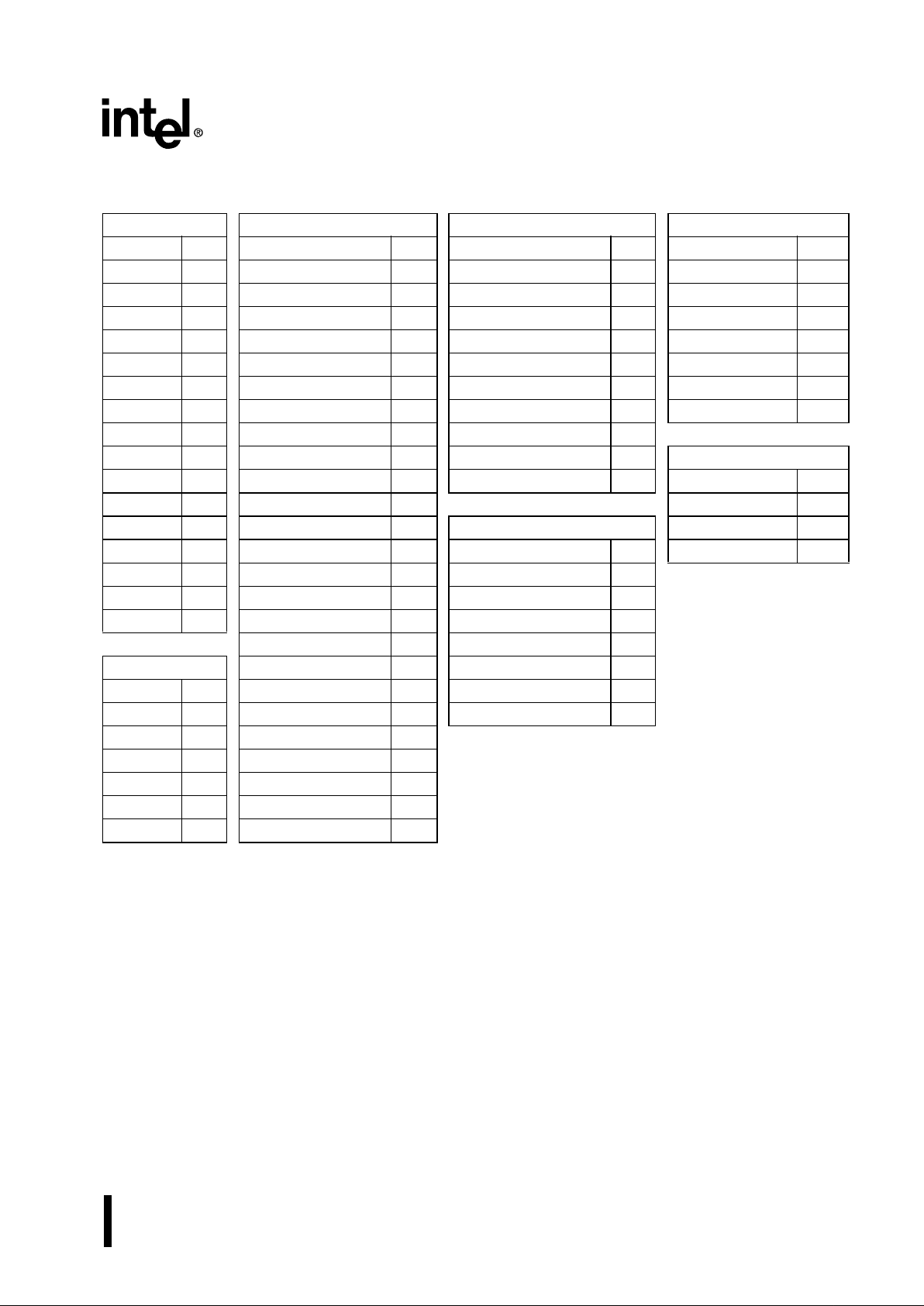
Table 3. Pin Assignment Arranged by Functional Categories
Addr & Data Input/Output Input/Output (Cont’d) Processor Control
Name Pin Name Pin Name Pin Name Pin
AD0 22 P1.0/EPA0/T2CLK 44 P4.7 7 CLKOUT 32
AD1 21 P1.1/EPA1 43
P5.0 2 EA# 24
AD2 20 P1.2/EPA2/T2DIR 42
P5.2 6EXTINT 29
AD3 19 P1.3/EPA3 41
P5.3 5 ONCE# 31
AD4 18 P2.0/TXD 27
P6.0/EPA8 45 RESET# 23
AD5 17 P2.1/RXD 28
P6.1/EPA9 46 XTAL1 52
AD6 16
P2.2 29 P6.4/SC0 47 XTAL2 51
AD7 15
P2.4 30 P6.5/SD0 48
AD8 14
P2.6 31 P6.6/SC1 49 Bus Control & Status
AD9 13
P2.7 32 P6.7/SD1 50 Name Pin
AD10 12 P3.0 22
ADV#/ALE 2
AD11 11 P3.1 21 Power & Ground
RD# 5
AD12 10 P3.2 20 Name Pin
WR#/WRL# 6
AD13 9 P3.3 19
V
CC
26
AD14 8 P3.4 18
V
CC
40
AD15 7 P3.5 17
V
PP
4
P3.6 16
V
SS
1
Input P3.7 15
V
SS
3
Name Pin P4.0 14 V
SS
25
P0.2 33 P4.1 13 V
SS
39
P0.3 34 P4.2 12
P0.4 35 P4.3 11
P0.5 36 P4.4 10
P0.6 37 P4.5 9
P0.7 38 P4.6 8

6 ADVANCE INFORMATION
83C196LC, 83C196L D — AUTOMOTIVE
3.0 SIGNALS
Table 4. Signal Descriptions
Name Type Description
AD15:0 I/O Address/Data Lines
These pins provide a multiplexed address and data bus. During the address
phase of the bus cycle, address bits 0–15 are presented on the bus and can be
latched using ALE or ADV#. During the data phase, 8- or 16-bit data is
transferred.
AD7:0 share package pins with P3.7:0. AD15:8 share package pins with P4.7:0.
ADV# O Address Valid
This active-low output signal is asserted only during external memory
accesses. ADV# indicates that valid address information is available on the
system address/data bus. The signal remains low while a valid bus cycle is in
progress and is returned high as soon as the bus cycle completes.
An external latch can use this signal to demultiplex the address from the
address/data bus. A decoder can also use this signal to generate chip selects
for external memory.
ADV# shares a package pin with P5.0 and ALE.
ALE O Address Latch Enable
This active-high output signal is asserted only during external memory cycles.
ALE signals the start of an external bus cycle and indicates that valid address
information is available on the system address/data bus.
An external latch can use this signal to demultiplex the address from the
address/data bus.
CLKOUT O Output
Output of the internal clock generator. The CLKOUT frequency is ½ the
oscillator input frequency (F
XTAL1
). CLKOUT has a 50% duty cycle.
CLKOUT shares a package pin with P2.7
EA# I External Access
This input determines whether memory accesses to special-purpose and
program memory partitions are directed to internal or external memory. These
accesses are directed to internal memory if EA# is held high and to
externalmemory if EA# is held low. For an access to any other memory location,
the value of EA# is irrelevant.
EA# is sampled and latched only on the rising edge of RESET#. Changing the
level of EA# after reset has no effect.
EPA9:8
EPA3:0
I/O Event Processor Array (EPA) Capture/Compare Channels
High-speed input/output signals for the EPA capture/compare channels.
The EPA signals share package pins with the following signals:
EPA0/P1.0/T2CLK, EPA1/P1.1, EPA2/P1.2/T2DIR, EPA3/P1.3,
EPA8/P6.0/COMP0, and EPA9/P6.1/COMP1. EPA7 does not connect to a
package pin. It cannot be used to capture an event, but it can function as a
software timer. EPA6:4 are not implemented.
ADVANCE INFORMATION 7
AUTOMOTIVE — 83C196LC, 83C196LD
EXTINT I External Interrupt
In normal operating mode, a rising edge on EXTINT sets the EXTINT interrupt
pending bit. EXTINT is sampled during phase 2 (CLKOUT high). The minimum
high time is one state time.
In powerdown mode, asserting the EXTINT signal for at least 50 ns causes the
device to resume normal operation. The interrupt does not need to be enabled.
In idle mode, asserting any enabled interrupt causes the device to resume
normal operation.
EXTINT shares a package pin with P2.2.
ONCE# I On-circuit Emulation
Holding ONCE# low during the rising edge of RESET# places the
microcontroller into on-circuit emulation (ONCE) mode. This mode puts all pins
into a high-impedance state, thereby isolating the microcontroller from other
components in the system. The value of ONCE# is latched when the RESET#
pin goes inactive. While the microcontroller is in ONCE mode, you can debug
the system using a clip-on emulator.
To exit ONCE mode, reset the microcontroller by pulling the RESET# signal
low. To prevent inadvertent entry into ONCE mode, either configure this pin as
an output or hold it high during reset and ensure that your system meets the V
IH
specification.
ONCE# shares a package pin with P2.6.
P0.7:2 I Port 0
This is a high-impedance, input-only port. Port 0 pins should not be left floating.
P1.3:0 I/O Port 1
This is a standard bidirectional port that shares package pins with individually
selectable special-function signals.
Port 1 shares package pins with the following signals: P1.0/EPA0/T2CLK,
P1.1/EPA1 , P1.2/EPA2/T2DIR, P1.3/EPA3.
P2.7:6
P2.4
P2.2:0
I/O P ort 2
This is a standard bidirectional port that shares package pins with individually
selectable special-function signals.
P2.6 is multiplexed with the ONCE function. If this pin is held low during reset,
the device will enter ONCE mode, so exercise caution if you use this pin for
input. If you choose to configure this pin as an input, always hold it lowhigh
during reset and ensure that your system meets the V
IH
specification to prevent
inadvertent entry into ONCE mode.
Port 2 shares package pins with the following signals: P2.0/TXD, P2.1/RXD,
P2.2/EXTINT, P2.6/ONCE#, P2.7/CLKOUT.
P3.7:0 I/O Port 3
This is a memory-mapped, 8-bit, bidirectional port with programmable opendrain or complementary output modes. The pins are shared with the
multiplexed address/data bus, which has complementary drivers.
P3.7:0 share package pins with AD7:0.
Table 4. Signal Descriptions (Continued)
Name Type Description

8 ADVANCE INFORMATION
83C196LC, 83C196L D — AUTOMOTIVE
P4.7:0 I/0 Port 4
This is a memory-mapped, 8-bit, bidirectional port with open-drain or
complementary output modes. The pins are shared with the multiplexed
address/data bus, which has complementary drivers.
P4.7:0 share package pins with AD15:8.
P5.3:2
P5.0
I/O Port 5
This is a memory-mapped, bidirectional port.
Port 5 shares package pins with the following signals: P5.0/ADV#/ALE,
P5.2/WR#/WRL#/PLLEN, and P5.3/RD#. P5.1 and P5.7:4 are not
implemented.
P6.7:4
P6.1:0
OPort 6
This is a standardbidirectional port.
Port 6 shares package pins with the following signals: P6.0/EPA8/COMP0,
P6.1/EPA9/COMP1, P6.4/SC0, P6.5/SD0, P6.6/SC1, and P6.7/SD1.
RD# O Read
Read-signal output to external memory. RD# is asserted during external
memory reads.
RD# shares a package pin with P5.3.
RESET# I/O Reset
A level-sensitive reset input to, and an open-drain system reset output from, the
microcontroller. Either a falling edge on RESET# or an internal reset turns on a
pull-down transistor connected to the RESET# pin for 16 state times.
In the powerdown and idle modes, asserting RESET# causes the
microcontroller to reset and return to normal operating mode. After a reset, the
first instruction fetch is from 2080H.
RXD I/O Receive Serial Data
In modes 1, 2, and 3, RXD receives serial port input data. In mode 0, it
functions as either an input or an open-drain output for data.
RXD shares a package pin with P2.1.
SC1:0 I/O Clock Pins for SSIO0 and 1
SC0 shares a package pin with P6.4, and SC1 shares a package pin with P6.6.
SD1:0 I/O Data Pins for SSIO0 and 1
These pins are the data I/O pins for SSIO0 and 1. For transmissions, configure
SD
x
as a complementary output signal. For receptions, configure SDx as a
high-impedance input signal.
SD0 shares a package pin with P6.5, and SD1 shares a package pin with P6.7.
T2CLK I Timer 2 External Clock
External clock for timer 2. Timer 2 increments (or decrements) on both rising
and falling edges of T2CLK. It is also used in conjunction with T2DIR for
quadrature counting mode.
T2CLK shares a package pin with P1.0 and EPA0.
Table 4. Signal Descriptions (Continued)
Name Type Description

ADVANCE INFORMATION 9
AUTOMOTIVE — 83C196LC, 83C196LD
T2DIR I Timer 2 External Direction
External direction (up/down) for timer 2. Timer 2 increments when T2DIR is
high and decrements when it is low. It is also used in conjunction with T2CLK
for quadrature counting mode.
T2DIR shares a package pin with P1.2 and EPA2.
TXD O Transmit Serial Data
In serial I/O modes 1, 2, and 3, TXD transmits serial port output data. In mode
0, it is the serial clock output.
TXD shares a package pin with P2.0.
V
CC
PWR Digital Supply Voltage
Connect each V
CC
pin to the digital supply voltage.
V
PP
PWR P owerdown Ex it
V
PP
causes the device to exit powerdown mode when it is driven low for at least
50 ns. Use this method to exit powerdown only when using an external clock
source because it enables the internal phase clocks, but not the internal
oscillator.
If you do not plan to use the powerdown feature, connect V
PP
to VCC.
V
SS
GND Digital Circuit Ground
These pins supply ground for the digital circuitry. Connect each V
SS
pin to
ground through the lowest possible impedance path.
WR# O Write
†
This active-low output indicates that an external write is occurring. This signal is
asserted only during external memory writes.
WR# shares a package pin with P5.2 and WRL#.
†
When this pin is configured as a special-function signal (P5_MODE.2 = 1), the
chip configuration register 0 (CCR0) determines whether it functions as WR#
or WRL#. CCR0.2 = 1 selects WR#; CCR0.2 = 0 selects WRL#.
WRL# O Write Low
†
During 16-bit bus cycles, this active-low output signal is asserted for low-byte
writes and word writes to external memory. During 8-bit bus cycles, WRL# is
asserted for all write operations.
WRL# shares a package pin with P5.2 and WR#.
†
When this pin is configured as a special-function signal (P5_MODE.2 = 1), the
chip configuration register 0 (CCR0) determines whether it functions as WR#
or WRL#. CCR0.2 = 1 selects WR#; CCR0.2 = 0 selects WRL#.
Table 4. Signal Descriptions (Continued)
Name Type Description

10 ADVANCE INFORMATION
83C196LC, 83C196L D — AUTOMOTIVE
XTAL1 I Input Crystal/Resonator or External Clock Input
Input to the on-chip oscillator and the internal clock generators. The internal
clock generators provide the peripheral clocks, CPU clock, and CLKOUT
signal. When using an external clock source instead of the on-chip oscillator,
connect the clock input to XTAL1. The external clock signal must meet the V
IH
specification for XTAL1.
XTAL2 O Inverted Output for the Crystal/Resonator
Output of the on-chip oscillator inverter. Leave XTAL2 floating when the design
uses an external clock source instead of the on-chip oscillator.
Table 4. Signal Descriptions (Continued)
Name Type Description

ADVANCE INFORMATION 11
AUTOMOTIVE — 83C196LC, 83C196LD
4.0 ADDRESS MAP
5.0 ELECTRICAL CHARACTERISTICS
Table 5. Address Map
Hex Address Range
Description
Addressing
Modes
LC LD
FFFF
A000
FFFF
6000
External device (memory or I/O) connected to
address/data bus
Indirect or indexed
9FFF
2080
5FFF
2080
Program memory (internal nonvolatile or external memory);
see Note 1
Indirect or indexed
207F
2000
207F
2000
Special-purpose memory (internal nonvolatile or external
memory)
Indirect or indexed
1FFF
1FE0
1FFF
1FE0
Memory-mapped SFRs Indirect or indexed
1FDF
1F00
1FDF
1F00
Peripheral SFRs
Indirect, indexed, or
windowed direct
1EFF
1C00
1EFF
1C00
External device (memory or I/O) connected to
address/data bus; (future SFR expansion; see Note 2)
Indirect or indexed
1BFF
0600
1BFF
0600
External device (memory or I/O) connected to
address/data bus
Indirect or indexed
05FF
0400
— Internal code or data RAM Indirect or indexed
—
05FF
0180
External device (memory or I/O) connected to
address/data bus
Indirect or indexed
03FF
0100
017F
0100
Upper register file (general-purpose register RAM)
Indirect, indexed, or
windowed direct
00FF
0000
00FF
0000
Lower register file (register RAM, stack pointer, and CPU
SFRs)
Direct, indirect, or
indexed
NOTES:
1. After a reset, the microcontroller fetches its first instruction from 2080H.
2. The content or function of these locations may change in future microcontroller revisions, in which
case a program that relies on a location in this range might not function properly.
ABSOLUTE MAXIMUM RATINGS
Storage temperature ............................... –60° C to +150° C
Supply voltage with respect to V
SS
............. –0.5 V to +13.0 V
Power dissipation....................... ..... ..... ...... .................. 0.5 W
OPERATING CONDITIONS
†
TA (Ambient temperature under bias)........ –40° C to +125° C
V
CC
(Digital supply voltage) ......................... 4.50 V to 5.50 V
F
XTAL1
(Oscillator frequency)....................... 4 MHz to 22 MHz
NOTICE: This document contains information on
products in the sampling and initial production
phases of development. The specifications are
subject to change without notice. Verify with your
local Intel sales office that you have the latest
datasheet before finalizing a design.
†
WARNING: Stressing the device beyond the
“Absolute Maximum Ratings” may cause permanent damage. These are stress ratings only. Operation beyond the “Operating Conditions” is not
recommended and extended exposure beyond the
“Operating Conditions” may affect device
reliability.

12 ADVANCE INFORMATION
83C196LC, 83C196L D — AUTOMOTIVE
5.1 DC Characteristics
Table 6. DC Characteristics at VCC = 4.5V – 5.5V
Symbol Parameter Min Typical Max Units T est Conditions
I
CC
VCC supply current
(
–40° C to +125° C
ambient)
88 mA
F
XTAL1
= 20 MHZ,
V
CC
= VPP = 5.5V
(While device is in reset)
I
CC1
Active mode supply current (typical)
55 mA
I
IDLE
Idle mode current 20 40 mA F
XTAL1
= 20 MHz,
V
CC
= VPP = 5.5V
I
PD
Powerdown mode
current
50 TBD µA
VCC = VPP = 5.5V
(Note 6)
V
IL
Input low voltage
(all pins)
–0.5V 0.3 V
CC
V
V
IH
Input high voltage (all
pins)
0.7 V
CC
VCC + 0.5 V
V
OL
Output low voltage
(outputs configured as
complementary)
0.3
0.45
1.5
V
V
V
IOL = 200 µA (Notes 3, 5)
I
OL
= 3.2 mA
IOL = 7.0 mA
V
OH
Output high voltage
(outputs configured as
complementary)
VCC – 0.3
V
CC
– 0.7
VCC – 1.5
V
V
V
I
OH
= –200 µA (Notes 3, 5)
I
OH
= –3.2 mA
IOH = –7.0 mA
I
LI
Input leakage current
(standard inputs, ports
3 & 4)
± 10 µA VSS ≤ VIN ≤ V
CC
(Note 2)
I
LI1
Input leakage current
(port 0)
± 2.0 µA VSS ≤ VIN ≤ V
REF
I
IH
Input high current (NMI
pin)
+175 µA VSS ≤ VIN ≤ V
CC
V
OH2
Output high voltage in
reset
VCC – 1V V IOH = –15 µA (Note 1)
I
OH2
Output high current in
reset
–25
–45
–50
–120
–240
–280
µA
µA
µA
V
OH2
= VCC – 1.0V
V
OH2
= VCC – 2.5V
V
OH2
= VCC – 4.0V
R
RST
Reset pullup resistor 6K 65K Ω
NOTES:
1. All bidirectional pins except CLKOUT. CLKOUT is not pulled weakly high in reset. Bidirectional pins
include ports 1–6.
2. Standard input pins include XTAL1, EA#, RESET#, P0.7:2, and ports 1–6 when configured as inputs.
3. All bidirectional pins when configured as complementary outputs.
4. Device is static and should operate below 1 Hz, but is only tested down to 4 MHz.
5. Maxim um I
OL
or IOH currents per pin will be characterized and published at a later date. Target values
are ± 10 mA.
6. Typicals are based on a limited number of samples and are not guaranteed. The values listed are at
room temperature and V
CC
= 5.0V.

ADVANCE INFORMATION 13
AUTOMOTIVE — 83C196LC, 83C196LD
C
S
Pin capacitance
(any pin to V
SS
)
10 pF F
TEST
= 1.0 MHz
R
WPU
Weak pullup resistance
(approximate)
150K Ω (Note 6)
Table 6. DC Characteristics at V
CC
= 4.5V – 5.5V (Continued)
Symbol Parameter Min Typical Max Units Test Conditions
NOTES:
1. All bidirectional pins except CLKOUT. CLKOUT is not pulled weakly high in reset. Bidirectional pins
include ports 1–6.
2. Standard input pins include XTAL1, EA#, RESET#, P0.7:2, and ports 1–6 when configured as inputs.
3. All bidirectional pins when configured as complementary outputs.
4. Device is static and should operate below 1 Hz, but is only tested down to 4 MHz.
5. Maximum I
OL
or IOH currents per pin will be characterized and published at a later date. Target values
are ± 10 mA.
6. Typicals are based on a limited number of samples and are not guaranteed. The values listed are at
room temperature and V
CC
= 5.0V.

14 ADVANCE INFORMATION
83C196LC, 83C196L D — AUTOMOTIVE
5.2 AC Characteristics
Test Conditions: capacitive load on all pins = 100 pF, rise and fall times = 10 ns, F
XTAL1
= 22 MHz.
Table 7. AC Characteristics
Symbol Parameter Min Max Units
The 83C196LC, 83C196LD meets these specifications
F
XTAL1
Oscillator Frequency 4.0 22.0 MHz
(1)
T
XTAL1
Oscillator Period (1/F
XTAL1
) 45.45 200 ns
T
XHCH
XTAL1 High to CLKOUT High or Low 20 110 ns
(2)
T
CLCL
CLKOUT Cycle Time 2 T
XTAL1
ns
T
CHCL
CLKOUT High Period T
XTAL1
– 10 T
XTAL1
+ 15 ns
T
CLLH
CLKOUT Falling to ALE Rising –10 15 ns
T
LLCH
ALE Falling to CLKOUT Rising –20 15 ns
T
LHLH
ALE Cycle Time 4 T
XTAL1
ns
T
LHLL
ALE High Period T
XTAL1
– 10 T
XTAL1
+ 10 ns
T
AVLL
Address Setup to ALE Low T
XTAL1
– 15 ns
T
LLAX
Address Hold after ALE Low T
XTAL1
– 40 ns
T
LLRL
ALE Low to RD# Low T
XTAL1
– 30 ns
T
RLCL
RD# Low to CLKOUT Low –10 20 ns
T
RLRH
RD# Low to RD# High T
XTAL1
– 5 ns
T
RHLH
RD# High to ALE Rising T
XTAL1
T
XTAL1
+ 25 ns
(3)
T
RLAZ
RD# Low to Address Float 5 ns
(5)
T
LLWL
ALE Low to WR# Low T
XTAL1
– 10 ns
T
CLWL
CLKOUT Low to WR# Falling Edge –10 20 ns
T
QVWH
Data Valid to WR# High T
XTAL1
– 23 ns
T
CHWH
CLKOUT High to WR# Rising Edge –10 15 ns
T
WLWH
WR# Low to WR# High T
XTAL1
– 20 ns
T
WHQX
Data Hold after WR# High T
XTAL1
– 25 ns
T
WHLH
WR# High to ALE High T
XTAL1
– 10 T
XTAL1
+ 15 ns
(3)
T
WHAX
AD15:8 Hold after WR# High T
XTAL1
– 30
(4)
ns
T
RHAX
AD15:8 Hold after RD# High T
XTAL1
– 30
(4)
ns
NOTES:
1. Testing is performed at 4 MHz, however, the device is static by design and will typically operate below
1 Hz.
2. Typical specifications, not guaranteed.
3. Assuming back-to- back bus cyc les.
4. 8-bit bus only.
5. T
RLAZ
(max) = 5 ns by design.

ADVANCE INFORMATION 15
AUTOMOTIVE — 83C196LC, 83C196LD
The external memory system must meet these specifications
T
AVDV
Address Valid to Input Data Valid 3 T
XTAL1
– 55 ns
T
RLDV
RD# Low to Input Data Valid T
XTAL1
– 22 ns
T
CLDV
CLKOUT Low to Input Data Valid T
XTAL1
– 50 ns
T
RHDZ
RD# High to Input Data Float T
XTAL1
ns
T
RXDX
Data Hold after RD# Inactive 0 ns
Table 8. AC Timing Symbol Definitions
Character Signal(s)
A AD15:0
C CLKOUT
D AD15:0, AD7:0
LALE
Q AD15:0, AD7:0
R RD#
W WR#, WRL#
Character Condition
HHigh
L Low
V Valid
X No Longer Valid
Z Floating (low impedance)
Table 7. AC Characteristics (Continued)
Symbol Parameter Min Max Units
NOTES:
1. Testing is performed at 4 MHz, however, the device is static by design and will typically operate below
1 Hz.
2. Typical specifications, not guaranteed.
3. Assuming back-to-back bus cycles.
4. 8-bit bus only.
5. T
RLAZ
(max) = 5 ns by design.

16 ADVANCE INFORMATION
83C196LC, 83C196L D — AUTOMOTIVE
Figure 4. System Bus Timing
XTAL1
CLKOUT
ALE/ADV#
RD#
WR#
T
XTAL1
T
XHCH
T
CHCL
T
CLCL
T
CLLH
T
LLCH
T
LHLH
T
LHLL
T
LLRL
T
RLRH
T
RHLH
T
RHDZ
T
AVLL
T
LLAX
T
RLDV
Address Out Data In
T
AVDV
T
LLWL
T
WLWH
T
WHLH
T
QVWH
T
WHQX
Data OutAddress Out Address Out
High Address Out
T
WHAX
, T
RHAX
T
RLAZ
AD15:0
(read)
AD15:0
(write)
AD15:8
(8-bit data bus)
A4320-01

ADVANCE INFORMATION 17
AUTOMOTIVE — 83C196LC, 83C196LD
5.3 AC Characteristics — Serial Port, Shift Register Mode
Test Conditions: TA = –40°C to +125°C; VCC = 5.0V ± 10%; VSS = 0.0V; Load Capacitance = 100 pF
Figure 5. Serial Port Waveform — Shift Register Mode
Table 9. Serial Port Timing — Shift Register Mode
Symbol Parameter Min Max Units
T
XLXL
Serial port clock period 8 T
XTAL1
ns
T
XLXH
Serial port clock falling edge to rising edge 4 T
XTAL1
– 50 4 T
XTAL1
+ 50 ns
T
QVXH
Output data setup to clock high 3 T
XTAL1
ns
T
XHQX
Output data hold after clock high 2 T
XTAL1
– 50 ns
T
XHQV
Next output data valid after clock high 2 T
XTAL1
+ 50 ns
T
DVXH
Input data setup to clock high 2 T
XTAL1
+ 200 ns
T
XHDX
†
Input data hold after clock high 0 ns
T
XHQZ
†
Last clock high to output float 5 T
XTAL1
ns
†
Parameter not tested.
A2080-03
Valid
Valid
Valid Valid Valid Valid
Valid
Valid
RXDx
(In)
TXD
x
01 2
3
4
5
6
7
T
QVXH
T
XLXL
T
DVXH
T
XHQV
T
XHQZ
T
XHDX
T
XHQX
T
XLXH
RXDx
(Out)

18 ADVANCE INFORMATION
83C196LC, 83C196L D — AUTOMOTIVE
5.4 AC Characteristics — Synchronous Serial Port
Figure 6. Synchronous Seri al Port
Table 10. Synchronous Serial Port Timing
Symbol Parameter Min Max Units
T
CLCL
Synchronous Serial Port Clock period TBD TBD ns
T
CLCH
Synchronous Serial Port Clock falling edge to
rising edge
TBD TBD n s
T
D1VD
Setup time for MSB output TBD ns
T
CXDV
Setup time for D6:0 output 1.5t + 20 ns
T
CXDX
Output data hold after clock high 0.5t ns
T
DVCX
Setup time for input data 10 ns
T
DXCX
Input data hold after clock high t + 5 ns
MSB D6 D5 D4 D3 D2 D1 D0
valid valid valid valid valid valid valid
valid
1 8765432
1 8765432
SC
x
(normal
transfers)
SD
x
(out)
SD
x
(in)
SC
x
(handshaking
transfers)
Slave Receiver Pulls SC
x
low
A3233-02
T
CHCH
T
CHCL
T
CLCH
STE Bit
T
D1DV
T
CXDX
T
CXDV
T
DVCX
T
DXCX
Assumes that the SSIO is configured to sample incoming data on the rising clock edge and sample outgoing
data on the falling clock edge, and that the SSIO is configured to pull the clock signal low while the channel
is idle.
†
†

ADVANCE INFORMATION 19
AUTOMOTIVE — 83C196LC, 83C196LD
5.5 External Clock Drive
Figure 7. External Clock Drive Waveforms
Table 11. External Clock Drive
Symbol Parameter Min Max Units
1/T
XLXL
Oscillator Frequency 4.0 22 MHz
T
XLXL
Oscillator Period (T
XTAL1
) 45.45 200 ns
T
XHXX
High Time 0.35 T
XTAL1
0.65 T
XTAL1
ns
T
XLXX
Low Time 0.35 T
XTAL1
0.65 T
XTAL1
ns
T
XLXH
Rise Time 10 n s
T
XHXL
Fall Time 10 n s
T
XLXX
A2119-03
T
XHXX
T
XHXL
T
XLXL
0.3 V
CC
– 0.5 V
0.7 V
CC
+ 0.5 V
T
XLXH
0.7 VCC + 0.5 V
0.3 V
CC
– 0.5 V
XTAL1

20 ADVANCE INFORMATION
83C196LC, 83C196L D — AUTOMOTIVE
5.6 Test Output Waveforms
Figure 8. AC Testing Input, Output Waveforms
Figure 9. Float Waveforms
Test Points
2.0 V
0.8 V
Note:
AC testing inputs are driven at 3.5 V for a logic “1” and 0.45 V for a logic
“0”. Timing measurements are made at 2.0 V for a logic “1” and 0.8 V for
a logic “0”.
3.5 V
0.45 V
A2120-04
2.0 V
0.8 V
V
LOAD
V
LOAD
– 0.15 V
V
LOAD
+ 0.15 V
Timing Reference
Points
V
OH
– 0.15 V
V
OL
+ 0.15 V
Note:
For timing purposes, a port pin is no longer floating when a 150 mV change from load
voltage occurs and begins to float when a 150 mV change from the loading V
OH/VOL
level occurs with IOL/IOH ≤15 mA.
A2121-03

ADVANCE INFORMATION 21
AUTOMOTIVE — 83C196LC, 83C196LD
6.0 THERMAL CHARACTERISTICS
All thermal impedance data is approximate for static air conditions at 1 watt of power dissipation. Values will
change depending on operating conditions and the application. The Intel
Packaging Handbook
(order number
240800) describes Intel’s thermal impedance test methodology. The
Components Quality and Reliability
Handbook
(order number 210997) provides quality and reliability information.
7.0 DESIGN CONSIDERATIONS
The 83C196LC and 83C196LD are pin-compatible replacements for the 87C196JT and 87C196JR microcontrollers with the following exceptions.
• The synchronous serial I/O port was enhanced to provide more flexible communication to other devices;
however, it remains compatible with the 87C196JT and JR non-enhanced SSIO.
• The A/D converter was removed to optimize die size.
Follow these recommendations to help maintain hardware and software compatibility between 52-pin, 68-pin,
and future microcontrollers.
• Bus width. Since the 83C196LC and LD have neither a WRH# nor a BUSWIDTH pin, the microcontrollers
cannot dynamically switch between 8- and 16-bit bus widths. Program the CCBs to select 8-bit bus mode.
• Wait states. Since the 83C196LC and LD have no READY pin, the microcontrollers cannot rely on a
READY signal to control wait states. Program the CCBs to limit the number of wait states (0, 1, 2, or 3).
• Write cycle during reset. If the microcontroller is reset during a write cycle, the contents of the external
memory device may be corrupted.
• EPA7. This function exists in the83C196LC and LD, but the associated pin is omitted. You can use this
channel either as a software timer or to reset the timers.
• EPA timer reset/write conflict. If an EPA channel resets the timer at the same time your code writes to
the timer, it is indeterminate which action takes precedence. If your code uses an EPA channel to reset a
timer, do not write to the timer.
• Valid time matches. The timer must increment or decrement to the compare value for a valid match to
occur. Writing the compare value to the timer will not cause a match. Resetting the timer also will not
cause a match when the compare value is zero.
• NMI. Since the 83C196LC and LD have no NMI pin, the nonmaskable interrupt is not supported. Initialize
the NMI vector (at location 203EH) to point to a RET instruction. This method provides glitch protection
only.
Table 12. Thermal Characteristics
Package Type θ
JA
θ
JC
52-pin PLCC 42°C/W 15°C/W
NOTES:
1. θ
JA
= Thermal resistance between junction and the surrounding environment (ambient). Measure-
ments are taken 1 ft. away from case in static air flow environment.
θ
JC
= Thermal resistance between juction and package surface (case).
2. All values of θ
JA
and θJC may fluctuate depending on the environment (with or without airflow, and
how much airflow) and microcontroller power dissipation at temperature of operation. Typical varia-
tions are ± 2
°C/W.
3. Values listed are at a maximum power dissipation of 0.50 W.

22 ADVANCE INFORMATION
83C196LC, 83C196L D — AUTOMOTIVE
• I/O port pins. The following port pins do not exist in the 83C196LC and LD: P0.0–P0.1, P1.4–P1.7, P2.3
and P2.5, P5.1 and P5.4–P5.7, P6.2 and P6.3. Software can still read and write the associated Px_REG,
Px_MODE, and Px_DIR registers. Configure the registers for the removed pins as follows:
— Clear the corresponding Px_DIR bits. (Configures pins as complementary outputs.)
— Clear the corresponding Px_MODE bits. (Selects I/O port function.)
— Write either “0” or “1” to the corresponding Px_REG bits. (Effectively ties signals low or high.)
— Do not use the bits associated with the removed port pins for conditional branch instructions. Treat
these bits as reserved.
• P6.7:4. A value written to any of the upper four bits of P6_REG (bits 4–7) is held in a buffer until the corre-
sponding P6_MODE bit is cleared, at which time the value is loaded into the P6_REG bit. A value read
from a P6_REG bit is the value currently in the register, not the value in the buffer. Therefore, any change
to a P6_REG bit can be read only after the corresponding P6_MODE bit is cleared.
• Reading reserved memory locations. The 87C196JT and JQ implement a precharged peripheral bus
within the microcontroller that returns a logic one when reserved bits are read. The 83C196LC and LD use
a driven bus within the microcontroller that returns the last value driven on the peripheral data bus when
reserved bits are read.
8.0 83C196LC, 83C196LD ERRATA
There is no known device errata at this time.
9.0 DATASHEET REVISION HISTORY
This datasheet is valid for devices with an “A” at the end of the topside field process order (FPO) number.
Datasheets are changed as new device information becomes available. Verify with your local Intel sales
office that you have the latest version before finalizing a design or ordering devices.
 Loading...