*Other brands and names are the property of their respective owners.
Information in this document is provided in connection with Intel products. Intel assumes no liability whatsoever, including infringement of any patent or
copyright, for sale and use of Intel products except as provided in Intel’s Terms and Conditions of Sale for such products. Intel retains the right to make
changes to these specifications at any time, without notice. Microcomputer Products may have minor variations to this specification known as errata.
February 1995COPYRIGHT©INTEL CORPORATION, 1995 Order Number: 270679-005
8XC196KB
ADVANCED 16-BIT CHMOS MICROCONTROLLER
ROMless OR ROM
Automotive
Y
b
40§Ctoa125§C Ambient
Y
232 Bytes of On-Chip Register RAM
Y
8 Kbytes of On-Chip ROM (Optional)
Y
High-Performance CHMOS Process
Y
Register-to-Register Architecture
Y
10-Bit A/D Converter with S/H
Y
Five 8-Bit I/O Ports
Y
28 Interrupt Sources
Y
Pulse Width Modulated Output
Y
Powerdown and Idle Modes
Y
High Speed I/O Subsystem
Y
Dynamically Configurable 8/16-Bit
Buswidth
Y
Full Duplex Serial Port
Y
Dedicated Baud Rate Generator
Y
1.725 ms 16 x 16 Multiply
Y
3 ms 32/16 Divide
Y
16-Bit Watchdog Timer
Y
16-Bit Timer
Y
16-Bit Up/Down Counter w/Capture
Y
Four 16-Bit Software Timers
Y
HOLD/HOLDA Bus Protocol
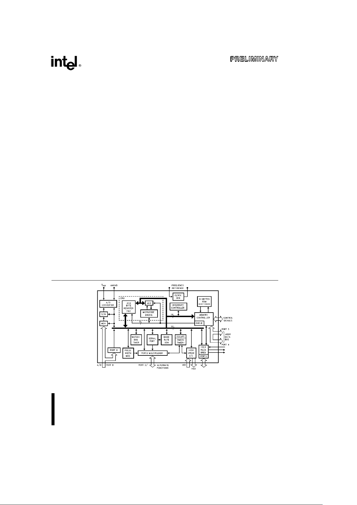
The 8XC196KB 16-bit microcontroller comes with 8 Kbytes of on-chip mask programmable ROM or in ROMless versions. All devices are high performance members of the 8096 microcontroller family. The 8XC196KB is
pin-to-pin compatible and uses a true superset of the 8096 instructions. Intel’s CHMOS process provides a
high performance processor along with low power consumption. To further reduce power requirements, the
processor can be placed into Idle or Powerdown Mode.
Bit, byte, word and some 32-bit operations are available on the 8XC196KB. With a 16 MHz oscillator, a 16-bit
addition takes 0.495 ms, and the instruction times average 0.375 ms to 1.125 ms in typical applications.
Four high-speed capture inputs are provided to record times when events occur. 4
a
2 high-speed outputs are
available for pulse or waveform generation. The high-speed output can also generate four software timers or
start an A/D conversion. Events can be based on the 16-bit timer or a 16-bit up/down counter.
Also provided on-chip are an 8 channel, 10-bit A/D converter with Sample and Hold, a serial port with
synchronous/asynchronous modes and on-chip baud rate generator, a 16-bit watchdog timer, pulse width
modulated output with prescaler and an on-chip clock failure detect circuitry.
270679– 1
Figure 1. 8XC196KB Block Diagram

AUTOMOTIVE 8XC196KB
270679– 3
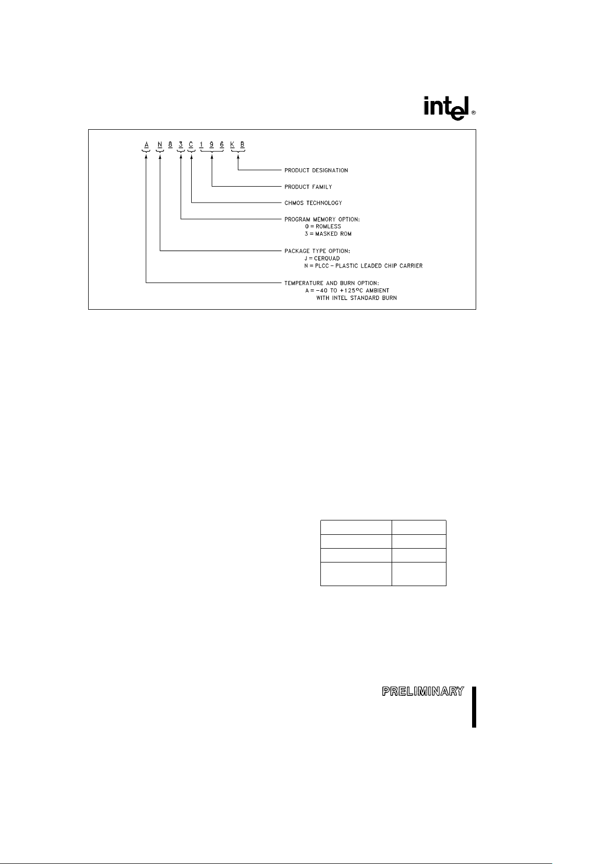
Figure 2. The 8XC196KB Family Nomenclature
ARCHITECTURE
The 8XC196KB is a member of the 8096 family, as
such has the same architecture and uses the same
instruction set as the 8096. Many new features have
been added on the 8CX196KB including:
CPU FEATURES
Divide by 2 instead of divide by 3 clock for a 1.5
c
performance improvement
Faster instructions, especially indexed/indirect data
operations
1.725 ms 16 x 16 multiply with 16 MHz clock (is
6.25 ms on the 8096)
Faster interrupt response (almost twice as fast)
Powerdown and Idle Modes
6 new instructions
8 new interrupt vectors/6 new interrupt sources
PERIPHERAL FEATURES
SFR window switching allows read-only SFRs to be
written and vice-versa
Timer 2 can count up and down by external selection
Timer 2 has an independent capture register on rising edges of (P2.7)
HSO line events are stored in a register
HSO has CAM lock and CAM clear commands
New baud rate values are needed for serial port,
which enables higher speeds in all modes.
Double buffered serial port transmit register (before,
only receive was double buffered)
Serial port receive overrun and framing error detection
PWM has a divide by 2 prescaler
HOLD/HLDA bus protocol
THERMAL CHARACTERISTICS
PLCC
i
JA
35§C/W
i
JC
12§C/W
Max Case
135
§
C
Temperature
NEW INSTRUCTIONS
PUSHA PUSHes the PSW, IMASK, IMASK1 and
WSR (used instead of PUSHF when using the new interrupts and registers)
POPA POPs the PSW, IMASK, IMASK1 and
WSR (used instead of POPF when using
the new interrupts and registers)
2

AUTOMOTIVE 8XC196KB
IDLPD Sets the device into Idle or Powerdown
Mode. The instruction has the following
format: IDLPD
Ý
key (where keye1 for
Idle and key
e
2 for Powerdown. Illegal
keys are processed, but no action is taken.
CMPL Compare 2 long direct values. Only the
direct addressing mode is supported for
this instruction and the format follows the
CMP format.
BMOV Block move using 2 auto-incrementing
pointers and a counter. The instruction
has the following format: BMOV
IPTR.wCNT. The IPTR is a long word,
with the low word being the address of
the source and the upper word being the
address of the destination. wCNT is the
number of words to be transferred.
DJNZW* Decrement Jump Not Zero using a word
counter. The instruction format follows
the DJNZ instruction.
*See the Functional Deviations section for details.
SFR OPERATION
All of the registers that were present on the 8096
work the same way as they did, except that the baud
rate value will be different on the 8XC196KB. The
new registers shown in the memory map control new
functions. The most important register is the Window
Select Register (WSR) which allows the reading of
the formerly write-only registers, and vice-versa.
PACKAGING
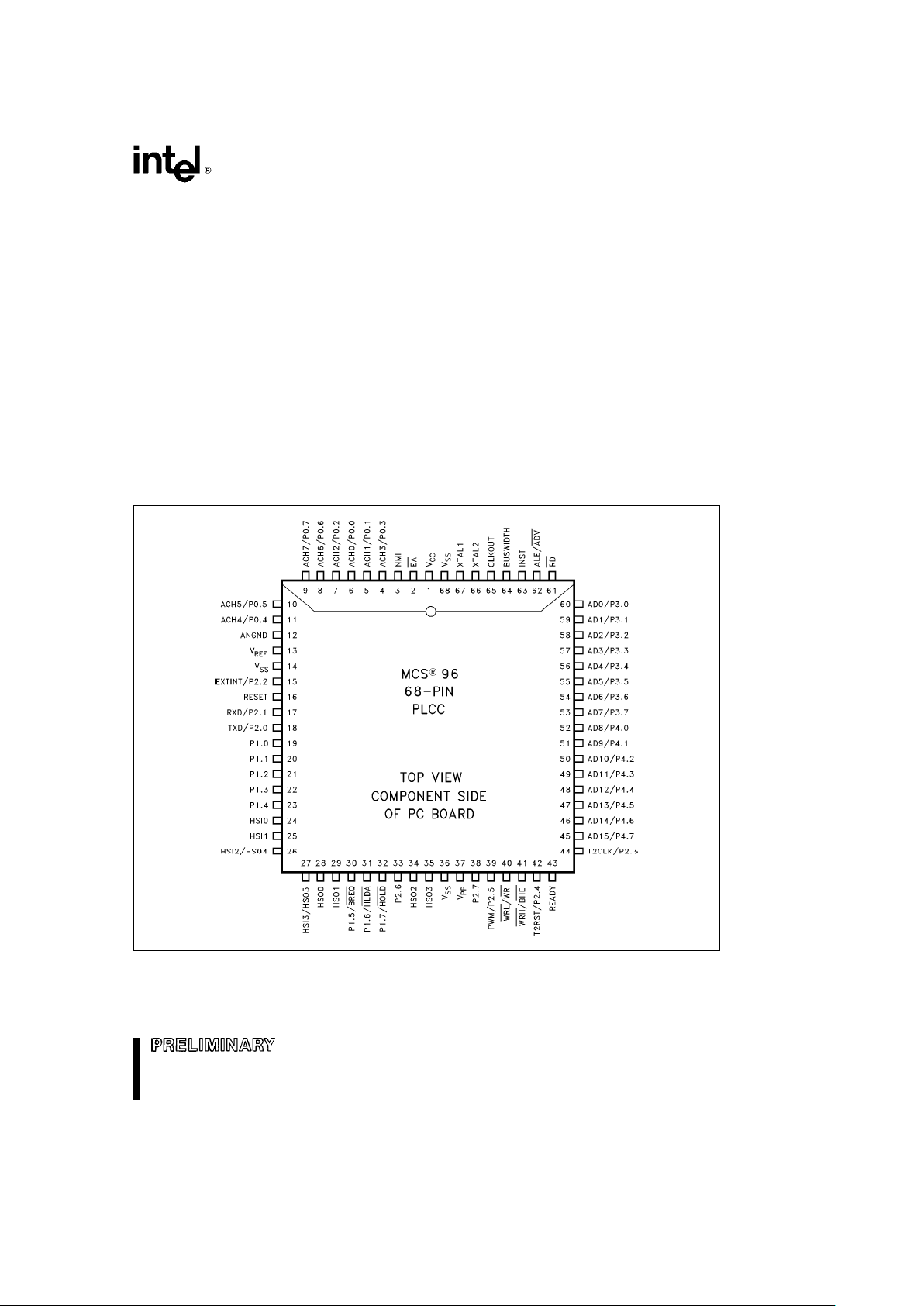
The 8XC196KB is available in 68-pin plastic leaded
chip carrier (PLCC) and 68-pin CERQUAD packages. Contact your local sales office to determine
the exact ordering code for the part desired.
270679– 2
Figure 3. 68-Pin PLCC Package
3

AUTOMOTIVE 8XC196KB
PLCC Description
9 ACH7/PO.7/PMD3
8 ACH6/PO.6/PMD2
7 ACH2/PO.2
6 ACH0/PO.0
5 ACH1/PO.1
4 ACH3/PO.3
3 NMI
2EA
1V
CC
68 V
SS
67 XTAL1
66 XTAL2
65 CLKOUT
64 BUSWIDTH
63 INST
62 ALE/ADV
61 RD
60 AD0/P3.0
59 AD1/P3.1
58 AD2/P3.2
57 AD3/P3.3
56 AD4/P3.4
55 AD5/P3.5
54 AD6/P3.6
53 AD7/P3.7
52 AD8/P4.0
51 AD9/P4.1
50 AD10/P4.2
49 AD11/P4.3
48 AD12/P4.4
47 AD13/P4.5
46 AD14/P4.6
45 AD15/P4.7
44 T2CLK/P2.3
PLCC Description
43 READY
42 T2RST/P2.4/AINC
41 BHE/WRH
40 WR/WRL
39 PWM/P2.5
38 P2.7/T2CAPTURE/PACT
37 V
PP
36 V
SS
35 HSO.3
34 HSO.2
33 P2.6
32 P1.7/HOLD
31 P1.6/HLDA
30 P1.5/BREQ
29 HSO.1
28 HSO.0
27 HSO.5/HSI.3/SID3
26 HSO.4/HSI.2/SID2
25 HSI.1/SID1
24 HSI.0/SID0
23 P1.4
22 P1.3
21 P1.2
20 P1.1
19 P1.0
18 TXD/P2.0/PVER
17 RXD/P2.1/PALE
16 RESET
15 EXTINT/P2.2/PROG
14 V
SS
13 V
REF
12 ANGND
11 ACH4/P0.4/PMD0
10 ACH4/P0.5/PMD1
Figure 4. PLCC Functional Pinouts
4

AUTOMOTIVE 8XC196KB
PIN DESCRIPTIONS
Symbol Name and Function
V
CC
Main Supply Voltage (a5V)
V
SS
Digital Circuit Ground (0V). There are three VSSpins, all of which MUST be connected.
V
REF
Reference for the A/D Converter (a5V). V
REF
is also the supply voltage to the analog portion
of the A/D converter and the logic used to read Port 0. Must be connected for A/D and Port 0
to function.
ANGND Reference Ground for the A/D Converter. Must be held at nominally the same potential as
V
SS
.
V
PP
Programming Voltage for the EPROM Parts. It should bea12.75V for programming. This pin
was V
BB
on 8X9X-90 parts. It is also the timing pin for the return from powerdown circuit.
Connect this pin with a 1 mF capacitor to V
SS
anda1MXresistor to VCC. If this function is not
used, V
PP
may be tied to VCC.
XTAL1 Input of the Oscillator Inverter and the Internal Clock Generator
XTAL2 Output of the Oscillator Inverter
CLKOUT Output of the Internal Clock Generator. The frequency of CLKOUT is (/2 the oscillator
frequency. It has a 50% duty cycle.
RESET Reset Input to the Chip. Input low for at least 4 state times will reset the chip. The subsequent
low to high transition resynchronizes CLKOUT and commences a 10-state time sequence in
which the PSW is cleared, a byte is read from 2018H loading the CCB, and a jump to location
2080H is executed. Input high for normal operation. RESET
has an internal pullup.
BUSWIDTH Input for Bus Width Selection. If CCR bit 1 is a one, this pin selects the buswidth for the bus
cycle in progress. If BUSWIDTH is low, an 8-bit cycle occurs. If BUSWIDTH is high, a 16-bit
cycle occurs. If CCR bit 1 is a 0, the bus is always an 8-bit bus. This pin is the TEST
pin on the
8X9X-90 parts. Systems with TEST
tied to VCCneed NOT change.
NMI A positive transition causes an interrupt vector through external memory location 203EH.
INST Output High during an External Memory Read. Indicates the read is an instruction fetch. INST
is valid throughout the bus cycle. INST is active only during external memory fetches, during
internal EPROM/ROM fetches INST is held low.
EA Input for Memory Select (External Access). EA equal to a TTL-high causes memory accesses
to locations 2000H through 3FFFH to be directed to on-chip EPROM/ROM. EA
equal to a
TTL-low causes accesses to these locations to be directed to off-chip memory. EA
e
a
12.75V causes execution to begin in the Programming Mode. EA has an internal pulldown,
so it defaults to execute from external memory, unless otherwise driven. EA
is latched at
reset.
ALE/ADV Address Latch Enable or Address Valid Output, as Selected by CCR. Both pin options provide
a latch to demultiplex the address from the address/data bus. When the pin is ADV, it goes
inactive (high) at the end of the bus cycle. ADV
can be used as a chip select for external
memory. ALE/ADV
is active only during external memory accesses.
5

AUTOMOTIVE 8XC196KB
PIN DESCRIPTIONS (Continued)
Symbol Name and Function
RD Read Signal Output to External Memory. RD is active only during external memory reads.
WR/WRL Write and Write Low Output to External Memory, as Selected by the CCR. WR will go low
for every external write, while WRL
will go low only for external writes where an even byte is
being written. WR
/WRL is active during external memory writes.
BHE/WRH Byte High Enable or Write High Output as Selected by the CCR. BHEe0 selects the bank
of memory that is connected to the high byte of the data bus. A0e0 selects that bank of
memory that is connected to the low byte. Thus accesses to a 16-bit wide memory can be
to the low byte only (A0
e
0, BHEe1), to the high byte only (A0e1, BHEe0) or both
bytes (A0
e
0, BHEe0). If the WRH function is selected, the pin will go low if the bus
cycle is writing to an odd memory location. BHE
/WRH is only valid during 16-bit external
memory write cycles.
READY Ready Input to lengthen external memory cycles, for interfacing with slow or dynamic
memory, or for bus sharing. If the pin is high, CPU operation continues in a normal manner.
If the pin is low prior to the falling edge of CLKOUT, the memory controller goes into a wait
state mode until the next positive transition in CLKOUT occurs with READY high. When
external memory is not used, READY has no effect. The number of wait states inserted into
the bus cycle is controlled by the CCR.
HSI Inputs to High Speed Input Unit. Four HSI pins are available: HSI.0, HSI.1, HSI.2, HSI.3.
Two of which are shared with the HSO Unit (HSI.2 and HSI.3). The HSI pins are also used
as the SID in Slave Programming Mode.
HSO Outputs from High Speed Output Unit. Six HSO pins are available (HSO.0 through HSO.5).
HSO.4 and HSO.5 are shared with HSI.
PORT 0 8-Bit High Impedance Input-Only Port. These pins can be used as digital inputs and/or as
analog inputs to the on-chip A/D converter. These pins are also used as inputs to EPROM
parts to select the Programming Mode.
PORT 1 8-Bit Quasi-Bidirectional I/O Port.
PORT 2 8-Bit Multi-Functional Port. All of its pins are shared with other functions.
PORT 3 and 4 8-Bit Bidirectional I/O Ports with Open Drain Outputs. These pins are shared with the
multiplexed address/data bus which has strong internal pullups.
HOLD Bus Hold Input Requesting Control of the Bus. Enabled by Setting WSR.7
HLDA Bus Hold Acknowledge Output Indicating Release of the Bus. Enabled by setting WSR.7.
BREQ Bus Request Output. Activated when the bus controller has a pending external memory
cycle. Enabled by setting WSR.7.
6
 Loading...