Intel Corporation AP28F010-150, AP28F010-120, AN28F010-150, AN28F010-120 Datasheet

*Other brands and names are the property of their respective owners.
Information in this document is provided in connection with Intel products. Intel assumes no liability whatsoever, including infringement of any patent or
copyright, for sale and use of Intel products except as provided in Intel’s Terms and Conditions of Sale for such products. Intel retains the right to make
changes to these specifications at any time, without notice. Microcomputer Products may have minor variations to this specification known as errata.
November 1995COPYRIGHT©INTEL CORPORATION, 1995 Order Number: 290266-004
A28F010
1024K (128K x 8) CMOS FLASH MEMORY
(Automotive)
Y
Automotive Temperature Range:
b
40§Ctoa125§C
Y
Flash Memory Electrical Chip-Erase
Ð 1 Second Typical Chip-Erase
Y
Quick-Pulse Programming Algorithm
Ð10 ms Typical Byte-Program
Ð 2 Second Chip-Program
Y
1,000 Erase/Program Cycles Minimum
over Automotive Temperature Range
Y
12.0Vg5% V
PP
Y
High-Performance Read
Ð 120 ns Maximum Access Time
Y
CMOS Low Power Consumption
Ð 30 mA Maximum Active Current
Ð 300 mA Maximum Standby Current
Y
Integrated Program/Erase Stop Timer
Y
Command Register Architecture for
Microprocessor/Microcontroller
Compatible Write Interface
Y
Noise Immunity Features
Ð
g
10% VCCTolerance
Ð Maximum Latch-Up Immunity
through EPI Processing
Y
ETOXTMIII Flash Nonvolatile Memory
Technology
Ð EPROM-Compatible Process Base
Ð High-Volume Manufacturing
Experience
Y
JEDEC-Standard Pinouts
Ð 32-Pin Plastic DIP
Ð 32-Lead PLCC
(See Packaging Spec., OrderÝ231369)
Intel’s 28F010 CMOS flash memory offers the most cost-effective and reliable alternative for read/write
random access nonvolatile memory. The 28F010 adds electrical chip-erasure and reprogramming to familiar
EPROM technology. Memory contents can be rewritten: in a test socket; in a PROM-programmer socket; onboard during subassembly test; in-system during final test; and in-system after-sale. The 28F010 increases
memory flexibility, while contributing to time- and cost-savings.
The 28F010 is a 1024-kilobit nonvolatile memory organized as 131,072 bytes of 8 bits. Intel’s 28F010 is
offered in 32-pin Plastic DIP or 32-lead PLCC packages. Pin assignments conform to JEDEC standards.
Extended erase and program cycling capability is designed into Intel’s ETOX
TM
III (EPROM Tunnel Oxide)
process technology. Advanced oxide processing, an optimized tunneling structure, and lower electric field
combine to extend reliable cycling beyond that of traditional EEPROMs. With the 12.0V V
PP
supply, the
28F010 performs a minimum of 1,000 erase and program cycles well within the time limits of the Quick-Pulse
Programming and Quick-Erase algorithms.
Intel’s 28F010 employs advanced CMOS circuitry for systems requiring high-performance access speeds, low
power consumption, and immunity to noise. Its 120 nanosecond access time provides no-WAIT-state performance for a wide range of microprocessors and microcontrollers. Maximum standby current of 300 mA translates into power savings when the device is deselected. Finally, the highest degree of latch-up protection is
achieved through Intel’s unique EPI processing. Prevention of latch-up is provided for stresses up to 100 mA
on address and data pins, from
b
1V to V
CC
a
1V.
With Intel’s ETOX III process base, the 28F010 leverages years of EPROM experience to yield the highest
levels of quality, reliability, and cost-effectiveness.
In order to meet the rigorous environmental requirements of automotive applications, Intel offers the 28F010 in
extended automotive temperature range. Read and write characteristics are guaranteed over the range of
b
40§Ctoa125§C ambient.

A28F010
290266– 1
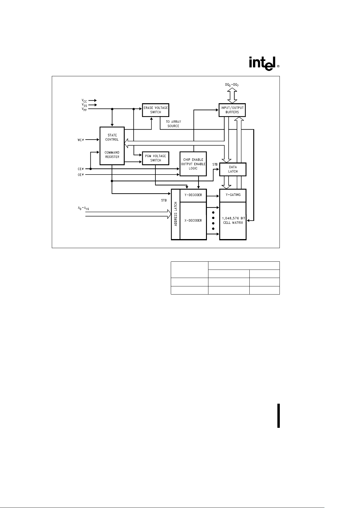
Figure 1. 28F010 Block Diagram
AUTOMOTIVE TEMPERATURE FLASH
MEMORIES
The Intel Automotive Flash memories have received
additional processing to enhance product characteristics. The automotive temperature range is
b
40§C
to
a
125§C during the read/write/erase/program
operations.
Versions
Speed
Packaging Options
Plastic DIP PLCC
150 AP AN
120 AP AN
2

A28F010
28F010
290266– 2
290266– 3
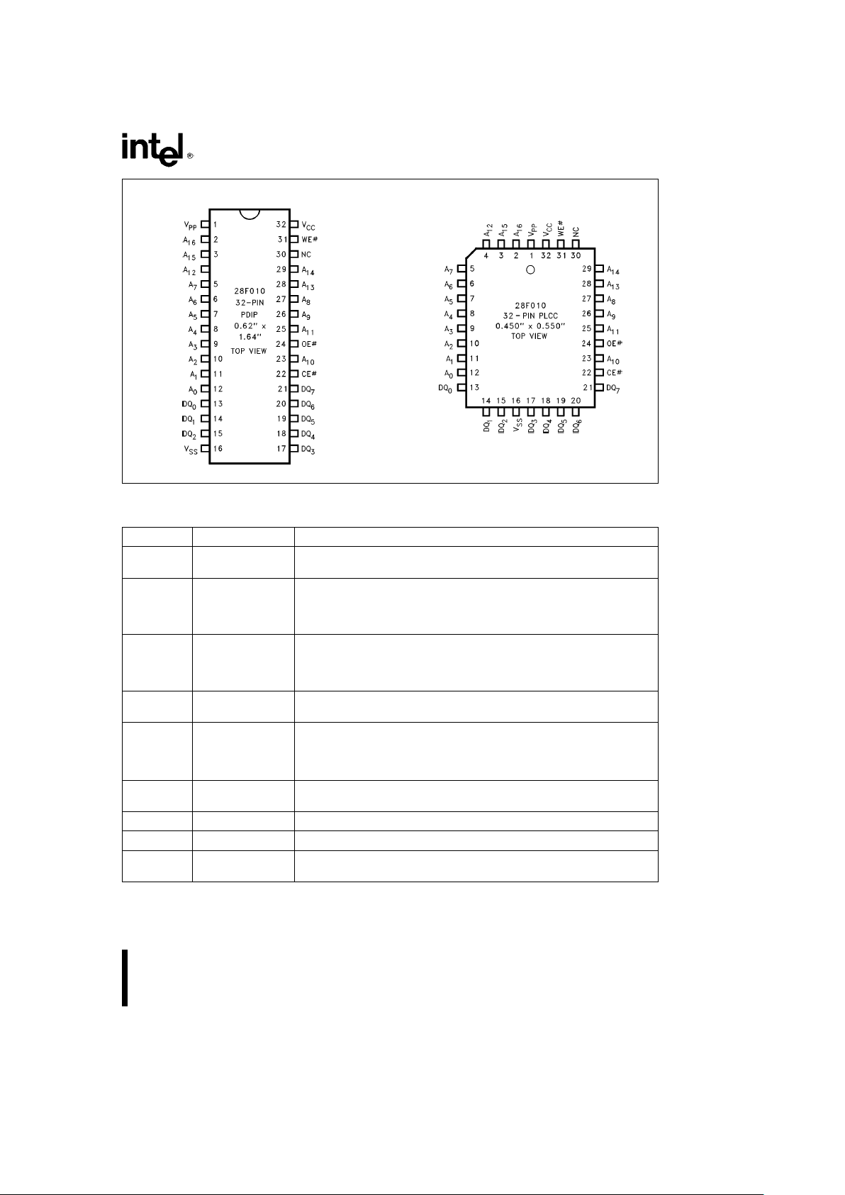
Figure 2. 28F010 Pin Configurations
Table 1. Pin Description
Symbol Type Name and Function
A0–A
16
INPUT ADDRESS INPUTS for memory addresses. Addresses are internally
latched during a write cycle.
DQ0–DQ7INPUT/OUTPUT DATA INPUT/OUTPUT: Inputs data during memory write cycles;
outputs data during memory read cycles. The data pins are active high
and float to tri-state OFF when the chip is deselected or the outputs
are disabled. Data is internally latched during a write cycle.
CE
Ý
INPUT CHIP ENABLE: Activates the device’s control logic, input buffers,
decoders and sense amplifiers. CE
Ý
is active low; CEÝhigh
deselects the memory device and reduces power consumption to
standby levels.
OE
Ý
INPUT OUTPUT ENABLE: Gates the devices output through the data buffers
during a read cycle. OE
Ý
is active low.
WE
Ý
INPUT WRITE ENABLE: Controls writes to the control register and the array.
Write enable is active low. Addresses are latched on the falling edge
and data is latched on the rising edge of the WE
Ý
pulse.
Note: With V
PP
s
6.5V, memory contents cannot be altered.
V
PP
ERASE/PROGRAM POWER SUPPLY for writing the command
register, erasing the entire array, or programming bytes in the array.
V
CC
DEVICE POWER SUPPLY (5Vg10%)
V
SS
GROUND
NC NO INTERNAL CONNECTION to device. Pin may be driven or left
floating.
3

A28F010
APPLICATIONS
The 28F010 flash-memory adds electrical chip-erasure and reprogrammability to EPROM non-volatility
and ease of use. The 28F010 is ideal for storing
code or data-tables in applications where periodic
updates are required. The 28F010 also serves as a
dense, nonvolatile data acquisition and storage medium.
The need for code updates pervades all phases of a
system’s lifeÐfrom prototyping to system manufacture to after-sale service. In the factory, during prototyping, revisions to control code necessitate ultraviolet erasure and reprogramming of EPROM-based
prototype codes. The 28F010 replaces the 15- to
20-minute ultraviolet erasure with one-second electrical erasure. Electrical chip-erasure and reprogramming occur in the same workstation or PROMprogrammer socket.
Diagnostics, performed at subassembly or final assembly stages, often require the socketing of
EPROMs. Socketed test codes are ultimately replaced with EPROMs containing the final program.
With electrical chip-erasure and reprogramming, the
28F010 is soldered to the circuit board. Test codes
are programmed into the 28F010 as it resides on the
circuit board. Ultimately, the final code can be downloaded to the device. The 28F010’s in-circuit alterability eliminates unnecessary handling and less-reliable socketed connections, while adding greater
test flexibility.
Material and labor costs associated with code
changes increase at higher levels of system integrationÐthe most costly being code updates after sale.
Code ‘‘bugs’’, or the desire to augment system functionality, prompt after-sale code updates. Field revisions to EPROM-based code require the removal of
EPROM components or entire boards.
Designing with the in-circuit alterable 28F010 eliminates socketed memories, reduces overall material
costs, and drastically cuts the labor costs associated with code updates. With the 28F010, code updates are implemented locally via an edge-connector, or remotely over a serial communication link.
The 28F010’s electrical chip-erasure, byte reprogrammability, and complete nonvolatility fit well with
data accumulation needs. Electrical chip-erasure
gives the designer a ‘‘blank-slate’’ in which to log
data. Data can be periodically off-loaded for analysisÐerasing the slate and repeating the cycle. Or,
multiple devices can maintain a ‘‘rolling window’’ of
accumulated data.
With high density, nonvolatility, and extended cycling
capability, the 28F010 offers an innovative alternative for mass storage. Integrating main memory and
backup storage functions into directly executable
flash memory boosts system performance, shrinks
system size, and cuts power consumption. Reliability
exceeds that of electromechanical media, with
greater durability in extreme environmental conditions.
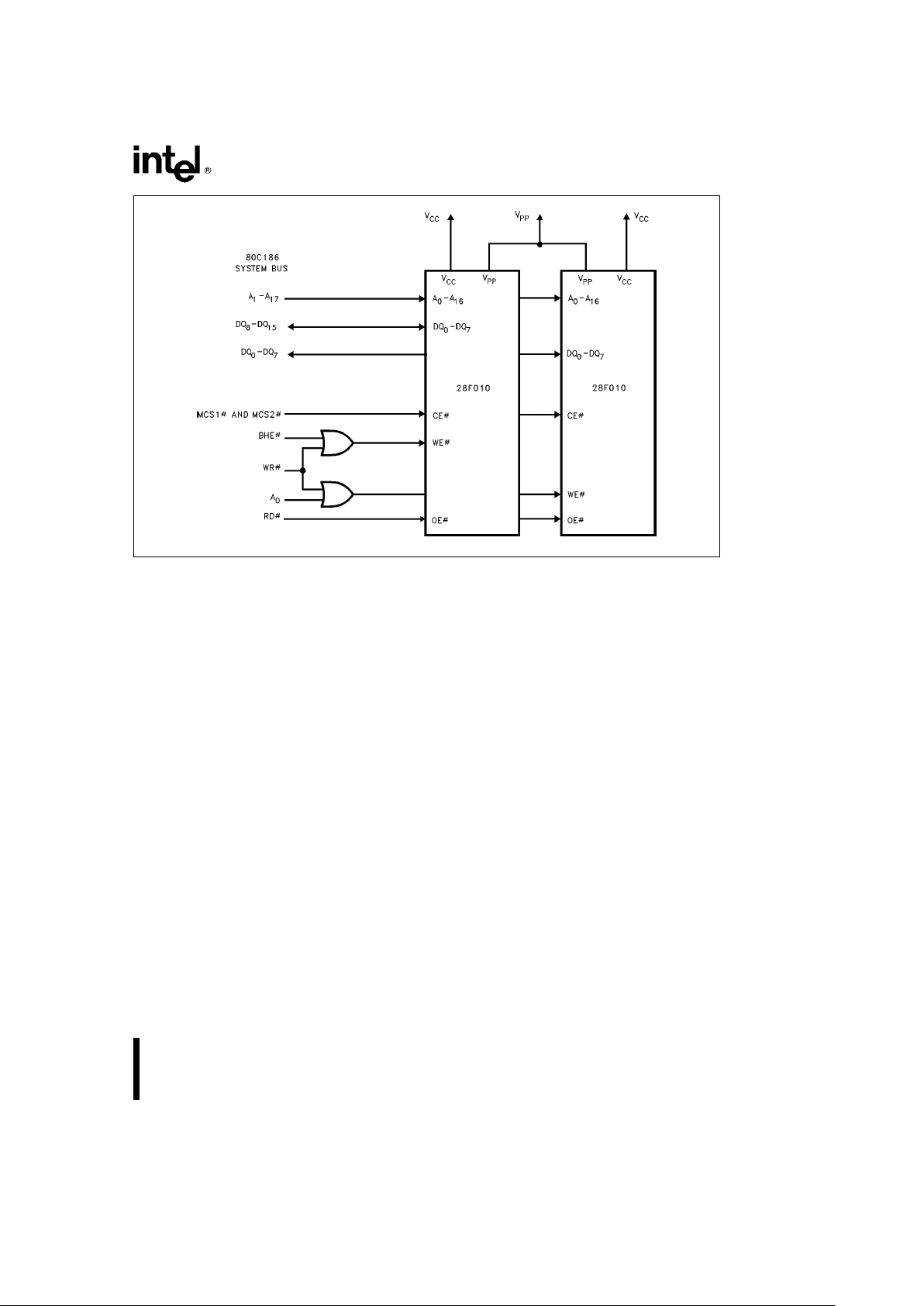
A high degree of on-chip feature integration simplifies memory-to-processor interfacing. Figure 3 depicts two 28F010s tied to the 80C186 system bus.
The 28F010’s architecture minimizes interface circuitry needed for complete in-circuit updates of
memory contents.
With cost-effective in-system reprogramming and
extended cycling capability, the 28F010 fills the
functionality gap between traditional EPROMs and
EEPROMs. EPROM-compatible specifications,
straightforward interfacing, and in-circuit alterability
allows designers to easily augment memory flexibility and satisfy the need for updatable nonvolatile
storage in today’s designs.
4

A28F010
290266– 4
Figure 3. 28F010 in a 80C186 System
PRINCIPLES OF OPERATION
Flash-memory augments EPROM functionality with
in-circuit electrical erasure and reprogramming. The
28F010 introduces a command register to manage
this new functionality. The command register allows
for: 100% TTL-level control inputs; fixed power supplies during erasure and programming; and maximum EPROM compatibility.
In the absence of high voltage on the V
PP
pin, the
28F010 is a read-only memory. Manipulation of the
external memory-control pins yields the standard
EPROM read, standby, output disable, and Intelligent Identifier operations.
The same EPROM read, standby, and output disable
operations are available when high voltage is applied to the V
PP
pin. In addition, high voltage on V
PP
enables erasure and programming of the device. All
functions associated with altering memory contentsÐIntelligent Identifier, erase, erase verify, program, and program verifyÐare accessed via the
command register.
Commands are written to the register using standard
microprocessor write timings. Register contents
serve as input to an internal state-machine which
controls the erase and programming circuitry. Write
cycles also internally latch addresses and data
needed for programming or erase operations. With
the appropriate command written to the register,
standard microprocessor read timings output array
data, access the Intelligent Identifier codes, or output data for erase and program verification.
Integrated Program/Erase Stop Timer
Successive command write cycles define the durations of program and erase operations; specifically,
the program or erase time durations are normally
terminated by associated program or erase verify
commands. An integrated stop timer provides simplified timing control over these operations; thus eliminating the need for maximum program/erase timing
specifications. Program and erase pulse durations
are minimums only. When the stop timer terminates
a program or erase operation, the device enters an
inactive state and remains inactive until receiving the
appropriate verify or reset command.
Write Protection
The command register is only alterable when VPPis
at high voltage. Depending upon the application, the
system designer may choose to make the V
PP
power supply switchableÐavailable only when memory
updates are desired. When high voltage is removed,
5

A28F010
Table 2. 28F010 Bus Operations
Pins
V
PP
(1)
A0A9CEÝOEÝWEÝDQ0–DQ
7
Operation
Read V
PPLA0
A
9
V
IL
V
IL
VIHData Out
Output Disable V
PPL
XXVILV
IH
VIHTri-State
READ-ONLY
Standby V
PPL
XXVIHX X Tri-State
Intelligent Identifier (Mfr)
(2)
V
PPLVILVID
(3)
V
IL
V
IL
VIHDatae89H
Intelligent Identifier (Device)
(2)
V
PPLVIHVID
(3)
V
IL
V
IL
VIHDataeB4H
Read V
PPHA0
A
9
V
IL
V
IL
VIHData Out
(4)
READ/WRITE
Output Disable V
PPH
XXVILV
IH
VIHTri-State
Standby
(5)
V
PPH
XXVIHX X Tri-State
Write V
PPHA0
A
9
V
ILVIH
VILData In
(6)
NOTES:
1. V
PPL
may be ground, a no-connect with a resistor tied to ground, ors6.5V. V
PPH
is the programming voltage specified
for the device. Refer to D.C. Characteristics. When V
PP
e
V
PPL
memory contents can be read but not written or erased.
2. Manufacturer and device codes may also be accessed via a command register write sequence. Refer to Table 3. All other
addresses low.
3. V
ID
is the Intelligent Identifier high voltage. Refer to DC Characteristics.
4. Read operations with V
PP
e
V
PPH
may access array data or the Intelligent Identifier codes.
5. With V
PP
at high voltage, the standby current equals I
CC
a
IPP(standby).
6. Refer to Table 3 for valid Data-In during a write operation.
7. X can be V
IL
or VIH.
the contents of the register default to the read command, making the 28F010 a read-only memory.
Memory contents cannot be altered.
Or, the system designer may choose to ‘‘hardwire’’
V
PP
, making the high voltage supply constantly
available. In this instance, all operations are performed in conjunction with the command register.
The 28F010 is designed to accommodate either design practice, and to encourage optimization of the
processor-memory interface.
The two-step Program/Erase write sequence to the
Command Register provides additional software
write protection.
BUS OPERATIONS
Read
The 28F010 has two control functions, both of which
must be logically active, to obtain data at the outputs. Chip-Enable (CE
Ý
) is the power control and
should be used for device selection. Output-Enable
(OE
Ý
) is the output control and should be used to
gate data from the output pins, independent of device selection. Figure 6 illustrates read timing waveforms.
When V
PP
is low (V
PPL
), the read only operation is
active. This permits reading the data in the array and
outputting the Intelligent Identifier codes (see Ta-
ble 2). When V
PP
is high (V
PPH
), the default condition of the device is the read only mode. This allows
reading the data in the array. Further functionality is
achieved though the Command Register as shown
in Table 3.
Output Disable
With Output-Enable at a logic-high level (V
IH
), output
from the device is disabled. Output pins are placed
in a high-impedance state.
Standby
With Chip-Enable at a logic-high level, the standby
operation disables most of the 28F010’s circuitry
and substantially reduces device power consumption. The outputs are placed in a high-impedance
state, independent of the Output-Enable signal. If
the 28F010 is deselected during erasure, programming, or program/erase verification, the device
draws active current until the operation is terminated.
Intelligent Identifier Operation
The Intelligent Identifier operation outputs the manufacturer code (89H) and device code (B4H). Programming equipment automatically matches the
device with its proper erase and programming
algorithms.
6

A28F010
With Chip-Enable and Output-Enable at a logic low
level, raising A9 to high voltage V
ID
(see DC Characteristics) activates the operation. Data read from locations 0000H and 0001H represent the manufacturer’s code and the device code, respectively.
The manufacturer- and device-codes can also be
read via the command register, for instances where
the 28F010 is erased and reprogrammed in the target system. Following a write of 90H to the command register, a read from address location 0000H
outputs the manufacturer code (89H). A read from
address 0001H outputs the device code (B4H).
Write
Device erasure and programming are accomplished
via the command register, when high voltage is applied to the V
PP
pin. The contents of the register
serve as input to the internal state-machine. The
state-machine outputs dictate the function of the
device.
The command register itself does not occupy an addressable memory location. The register is a latch
used to store the command, along with address and
data information needed to execute the command.
The command register is written by bringing WriteEnable to a logic-low level (V
IL
), while Chip-Enable is
low. Addresses are latched on the falling edge of
Write-Enable, while data is latched on the rising
edge of the Write-Enable pulse. Standard microprocessor write timings are used.
Refer to A.C. Write Characteristics and the Erase/
Programming Waveforms for specific timing
parameters.
COMMAND DEFINITIONS
When low voltage is applied to the V
PP
pin, the contents of the command register default to 00H, enabling read-only operations.
Placing high voltage on the V
PP
pin enables read/
write operations. Device operations are selected by
writing specific data patterns into the command register. Table 3 defines these 28F010 register
commands.
Table 3. Command Definitions
Bus
First Bus Cycle Second Bus Cycle
Command Cycles
Req’d Operation
(1)
Address
(2)
Data
(3)
Operation
(1)
Address
(2)
Data
(3)
Read Memory 1 Write X 00H
Read Intelligent Identifier Codes
(4)
2 Write X 90H Read IA ID
Set-up Erase/Erase
(5)
2 Write X 20H Write X 20H
Erase Verify
(5)
2 Write EA A0H Read X EVD
Set-up Program/Program
(6)
2 Write X 40H Write PA PD
Program Verify
(6)
2 Write X C0H Read X PVD
Reset
(7)
2 Write X FFH Write X FFH
NOTES:
1. Bus operations are defined in Table 2.
2. IA
e
Identifier address: 00H for manufacturer code, 01H for device code.
EA
e
Address of memory location to be read during erase verify.
PA
e
Address of memory location to be programmed.
Addresses are latched on the falling edge of the Write-Enable pulse.
3. ID
e
Data read from location IA during device identification (Mfre89H, DeviceeB4H).
EVD
e
Data read from location EA during erase verify.
PD
e
Data to be programmed at location PA. Data is latched on the rising edge of Write-Enable.
PVD
e
Data read from location PA during program verify. PA is latched on the Program command.
4. Following the Read Intelligent ID command, two read operations access manufacturer and device codes.
5. Figure 5 illustrates the Quick-Erase Algorithm.
6. Figure 4 illustrates the Quick-Pulse Programming Algorithm.
7. The second bus cycle must be followed by the desired command register write.
7
