

Intel Corporation A82596SX, A82596DX Datasheet
*Other brands and names are the property of their respective owners.
Information in this document is provided in connection with Intel products. Intel assumes no liability whatsoever, including infringement of any patent or
copyright, for sale and use of Intel products except as provided in Intel’s Terms and Conditions of Sale for such products. Intel retains the right to make
changes to these specifications at any time, without notice. Microcomputer Products may have minor variations to this specification known as errata.
November 1995COPYRIGHT©INTEL CORPORATION, 1996 Order Number: 290219-006
82596DX AND 82596SX
HIGH-PERFORMANCE 32-BIT LOCAL
AREA NETWORK COPROCESSOR
Y
Performs Complete CSMA/CD Medium
Access Control (MAC) FunctionsÐ
Independently of CPU
Ð IEEE 802.3 (EOC) Frame Delimiting
Y
Supports Industry Standard LANs
Ð IEEE TYPE 10BASE-T (TPE),
IEEE TYPE 10BASE5 (Ethernet*),
IEEE TYPE 10BASE2 (Cheapernet),
IEEE TYPE 1BASE5 (StarLAN),
and the Proposed Standard
TYPE 10BASE-F
Ð Proprietary CSMA/CD Networks Up
to 20 Mb/s
Y
On-Chip Memory Management
Ð Automatic Buffer Chaining
Ð Buffer Reclamation after Receipt of
Bad Frames; Optional Save Bad
Frames
Ð 32-Bit Segmented or Linear (Flat)
Memory Addressing Formats
Y
82586 Software Compatible
Y
Optimized CPU Interface
Ð 82596DX Bus Interface Optimized to
Intel’s 32-Bit i386
TM
DX
Ð 82596SX Bus Interface Optimized to
Intel’s 16-Bit i386
TM
SX
Ð Supports Big Endian and Little
Endian Byte Ordering
Y
High-Performance 16-/32-Bit Bus
Master Interface
Ð 66-MB/s Bus Bandwidth
Ð 33-MHz Clock, Two Clocks Per
Transfer
Ð Bus Throttle Timers
Ð Transfers Data at 100% of Serial
Bandwidth
Ð 128-Byte Receive FIFO, 64-Byte
Transmit FIFO
Y
Network Management and Diagnostics
Ð Monitor Mode
Ð 32-Bit Statistical Counters
Y
Self-Test Diagnostics
Y
Configurable Initialization Root for Data
Structures
Y
High-Speed, 5-V, CHMOS** IV
Technology
Y
132-Pin Plastic Quad Flat Pack (PQFP)
and PGA Package
(See Packaging Specifications Order Number: 240800-001,
Package Type KU and A)
i386
TM
is a trademark of Intel Corporation
*Ethernet is a registered trademark of Xerox Corporation.
**CHMOS is a patented process of Intel Corporation.
290219– 1
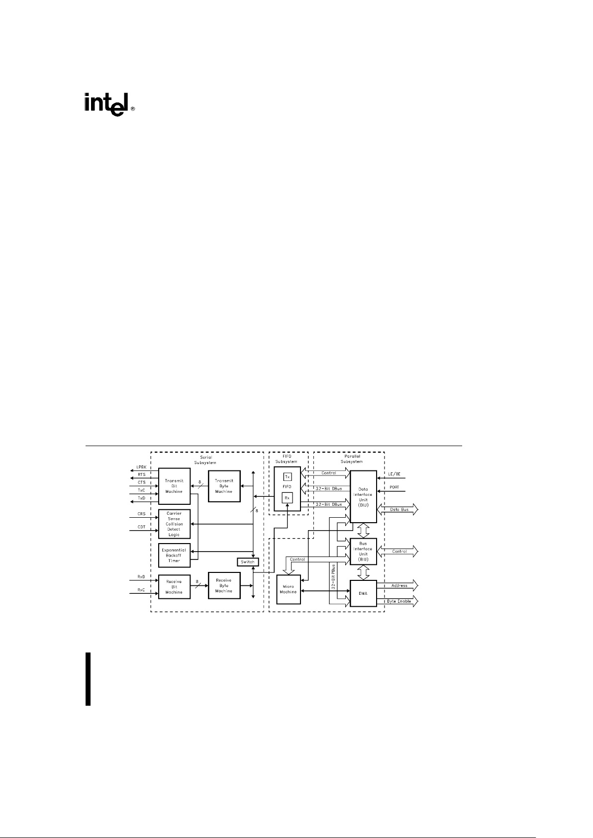
Figure 1. 82596DX/SX Block Diagram

82596DX/SX
82596DX and 82596SX High-Performance
32-Bit Local Area Network Coprocessor
CONTENTS PAGE
INTRODUCTION
ААААААААААААААААААААААААААА 3
PIN DESCRIPTIONS АААААААААААААААААААААА 10
82596 AND HOST CPU
INTERACTION ААААААААААААААААААААААААА 14
82596 BUS INTERFACE АААААААААААААААААА 14
82596 MEMORY ADDRESSING АААААААААА 14
82596 SYSTEM MEMORY
STRUCTURE ААААААААААААААААААААААААААА 16
TRANSMIT AND RECEIVE MEMORY
STRUCTURES
ААААААААААААААААААААААААА 17
TRANSMITTING FRAMES АААААААААААААААА 20
RECEIVING FRAMES АААААААААААААААААААА 21
82596 NETWORK MANAGEMENT AND
DIAGNOSTICS ААААААААААААААААААААААААА 21
NETWORK PLANNING AND
MAINTENANCE АААААААААААААААААААААААА 23
STATION DIAGNOSTICS AND SELF-
TEST
ААААААААААААААААААААААААААААААААААА 24
82586 SOFTWARE COMPATIBILITY ААААА 24
INITIALIZING THE 82596 АААААААААААААААА 24
SYSTEM CONFIGURATION POINTER
(SCP) ААААААААААААААААААААААААААААААААААА 24
Writing the Sysbus АААААААААААААААААААААААА 25
INTERMEDIATE SYSTEM
CONFIGURATION POINTER
(ISCP)
АААААААААААААААААААААААААААААААААА 26
INITIALIZATION PROCESS АААААААААААААА 26
CONTROLLING THE 82596DX/SX ААААААА 27
82596 CPU ACCESS INTERFACE
(PORT
Ý
) ААААААААААААААААААААААААААААААА 27
MEMORY ADDRESSING FORMATS ААААА 28
LITTLE ENDIAN AND BIG ENDIAN
BYTE ORDERING
АААААААААААААААААААААА 28
COMMAND UNIT (CU) ААААААААААААААААААА 29
RECEIVE UNIT (RU) АААААААААААААААААААААА 30
SYSTEM CONTROL BLOCK (SCB) АААААА 30
SCB OFFSET ADDRESSES АААААААААААААА 33
CONTENTS PAGE
CBL Offset (Address)
ААААААААААААААААААААА 33
RFA Offset (Address) ААААААААААААААААААААА 34
SCB STATISTICAL COUNTERS АААААААААА 34
Statistical Counter Operation АААААААААААААА 34
ACTION COMMANDS AND
OPERATING MODES
АААААААААААААААААА 35
NOP АААААААААААААААААААААААААААААААААААААА 35
Individual Address Setup АААААААААААААААААА 36
Configure ААААААААААААААААААААААААААААААААА 37
Multicast-Setup ААААААААААААААААААААААААААА 43
Transmit АААААААААААААААААААААААААААААААААА 44
Jamming Rules ААААААААААААААААААААААААААА 46
TDR АААААААААААААААААААААААААААААААААААААА 47
Dump ААААААААААААААААААААААААААААААААААААА 49
Diagnose ААААААААААААААААААААААААААААААААА 52
RECEIVE FRAME DESCRIPTOR ААААААААА 52
Simplified Memory Structure ААААААААААААААА 53
Flexible Memory Structure ААААААААААААААААА 54
Receive Buffer Descriptor (RBD) ААААААА 55
PGA PACKAGE THERMAL
SPECIFICATION ААААААААААААААААААААААА 60
ELECTRICAL AND TIMING
CHARACTERISTICS
ААААААААААААААААААА 60
Absolute Maximum Ratings ААААААААААААААА 60
DC Characteristics АААААААААААААААААААААААА 60
AC Characteristics АААААААААААААААААААААААА 61
82596DX Input/Output System
Timings АААААААААААААААААААААААААААААА 61
82596SX Input/Output System
Timings
АААААААААААААААААААААААААААААА 63
Transmit/Receive Clock
Parameters АААААААААААААААААААААААААА 66
82596DX/SX BUS OPERATION АААААААААА 68
System Interface A.C. Timing
Characteristics АААААААААААААААААААААААААА 69
Input Waveforms АААААААААААААААААААААААААА 70
Serial A.C. Timing Characteristics АААААААААА 72
OUTLINE DIAGRAMS АААААААААААААААААААА 74
REVISION SUMMARY АААААААААААААААААААА 77
2

82596DX/SX
INTRODUCTION
The 82596DX/SX is an intelligent, high-performance
32-bit Local Area Network coprocessor. The
82596DX/SX implements the CSMA/CD access
method and can be configured to support all existing IEEE 802.3 standardsÐTYPEs 10BASE-T,
10BASE5, 10BASE2, 1BASE5, and 10BROAD36. It
can also be used to implement the proposed standard TYPE 10BASE-F. The 82596DX/SX performs
high-level commands, command chaining, and interprocessor communications via shared memory, thus
relieving the host CPU of many tasks associated
with network control. All time-critical functions are
performed independently of the CPU, this increases
network performance and efficiency. The
82596DX/SX bus interface is optimized for Intel’s
i386
TM
DX and i386TMSX microprocessors.
The 82596DX/SX implements all IEEE 802.3 Medium Access Control and channel interface functions,
these include framing, preamble generation and
stripping, source address generation, destination address checking, short-frame detection, and automatic length-field handling. Data rates up to 20 Mb/s are
supported.
The 82596DX/SX provides a powerful host system
interface. It manages memory structures automatically, with command chaining and bidirectional data
chaining. An on-chip DMA controller manages four
channels, this allows autonomous transfer of data
blocks (buffers and frames) and relieves the CPU of
byte transfer overhead. Buffers containing errored or
collided frames can be automatically recovered without CPU intervention. The 82596DX/SX provides an
upgrade path for existing 82586 software drivers by
providing an 82586-software-compatible mode that
supports the current 82586 memory structure. The
82596DX/SX also has a Flexible memory structure
and a Simplified memory structure. The 82596DX/
SX can address up to 4 gigabytes of memory. The
82596DX/SX supports Little Endian and Big Endian
byte ordering.
The 82596DX/SX bus interface is optimized to Intel’s i386
TM
DX and i386 SX microprocessors, providing a bus transfer rate of up to 66 MB/s at
33 MHz. The bus interface employs bus throttle timers to regulate 82596DX/SX bus use. Two large, independent FIFOsÐ128 bytes for Receive and 64
bytes for TransmitÐtolerate long bus latencies and
provide programmable thresholds that allow the
user to optimize bus overhead for any worst-case
bus latency.
The 82596DX/SX provides a wide range of diagnostics and network management functions, these include internal and external loopback, exception condition tallies, channel activity indicators, optional
capture of all frames regardless of destination ad-
dress (promiscuous mode), optional capture of errored or collided frames, and time domain reflectometry for locating fault points on the network cable.
The statistical counters, in 32-bit segmented and linear modes, are 32-bits each and include CRC errors,
alignment errors, overrun errors, resource errors,
short frames, and received collisions. The
82596DX/SX also features a monitor mode for network analysis. In this mode the 82596DX/SX can
capture status bytes, and update statistical counters, of frames monitored on the link without transferring the contents of the frames to memory. This
can be done concurrently while transmitting and receiving frames destined for that station.
The 82596DX/SX can be used in both baseband
and broadband networks. It can be configured for
maximum network efficiency (minimum contention
overhead) with networks of any length. Its highly
flexible CSMA/CD unit supports address field
lengths of zero through six bytes for IEEE 802.3/
Ethernet frame delimitation. It also supports 16- or
32-bit cyclic redundancy checks. The CRC can be
transferred directly to memory for receive, operations or dynamically inserted for transmit operations.
The CSMA/CD unit can also be configured for full
duplex operation for high throughput in point-to-point
connections.
The 82596 C-Step incorporates several new features not found in previous steppings. The following
is a summary of the 82596 C-step’s new features.
#
The 82596 C-step fixes Errata found in the A1
and B steppings.
#
The 82596 C-step has improved AC timings over
both the A and B steppings.
#
The 82596 C-step has a New Enhanced Big Endian Mode where in Linear Addressing mode, true
32-bit Big Endian functionality is achieved. New
Enhanced Big Endian Mode is enabled by setting
bit 7 of the SYSBUS byte. This mode is software
compatible with the big endian mode of the Bstep with one exceptionÐno 32-bit addresses
need to be swapped by software in the C-step. In
this new mode, the 82596 C-step treats 32-bit address pointers as true 32-bit entities and the SCB
absolute address and statistical counters are still
treated as two 16-bit big endian entities. Not setting this mode will configure the 82596 C-step to
be 100% compatible to the A1-step bit endian
mode.
#
The 82596 C-step is hardware and software compatible to both the A1 and B steppings allowing
for easy ‘‘drop-in’’ to current designs. Pinout and
control structures remain unchanged.
The 82596DX/SX is fabricated with Intel’s reliable,
5-V, CHMOS IV (Process 648.8) technology. It is
available in a 132-pin PQFP or PGA package.
3

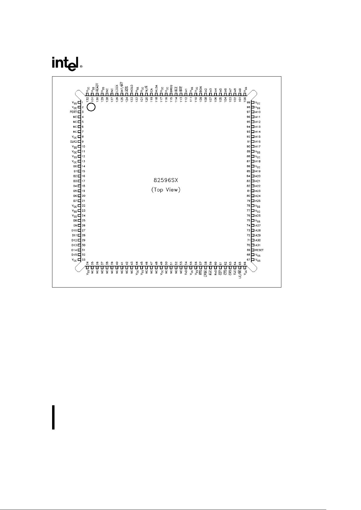
82596DX/SX
290219– 2
Figure 2a. 82596DX PQFP Pin Configuration
4
82596DX/SX
290219– 34
Figure 2b. 82596SX PQFP Pin Configuration
5
82596DX/SX
290219– 3
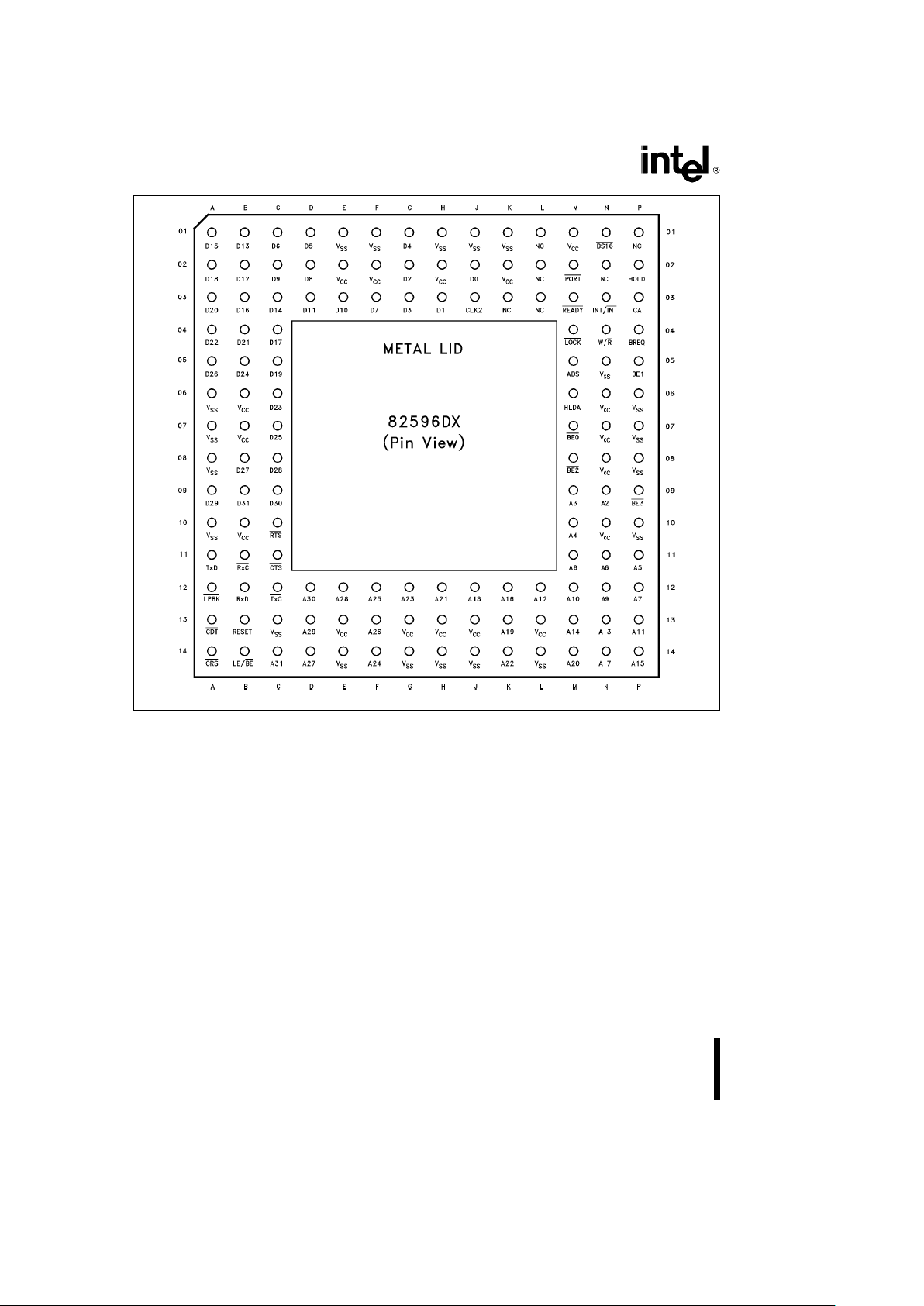
Figure 3a. 82596DX PGA Pin View Side
6
82596DX/SX
82596DX PGA Cross Reference by Pin Name
Address Data Control
Serial
N/C V
CC
V
SS
Interface
Signal Pin No. Signal Pin No. Signal Pin No. Signal Pin No. Pin No. Pin No. Pin No.
A
2
N9 D
0
J2 ADS M5 CDT A13 K3 B6 A6
A
3
M9 D
1
H3 BE0 M7 CRS A14 L1 B7 A7
A
4
M10 D
2
G2 BE1 P5 CTS C11 L2 B10 A8
A
5
P11 D
3
G3 BE2 M8 LPBK A12 L3 E2 A10
A
6
N11 D
4
G1 BE3 P9 RTS C10 N2 E13 C13
A
7
P12 D
5
D1 BREQ P4 RxC B11 P1 F2 E1
A
8
M11 D
6
C1 BS16 N1 RxD B12 G13 E14
A
9
N12 D
7
F3 CA P3 TxC C12 H2 F1
A
10
M12 D
8
D2 CLK2 J3 TxD A11 H13 G14
A
11
P13 D
9
C2 HLDA M6 J13 H1
A
12
L12 D
10
E3 HOLD P2 K2 H14
A
13
N13 D
11
D3 INT/INT N3 L13 J1
A
14
M13 D
12
B2 LE/BE B14 M1 J14
A
15
P14 D
13
B1 LOCK M4 N6 K1
A
16
K12 D
14
C3 PORT M2 N7 L14
A
17
N14 D
15
A1 READY M3 N8 N5
A
18
J12 D
16
B3 RESET B13 N10 P6
A
19
K13 D
17
C4 W/R N4 P7
A
20
M14 D
18
A2 P8
A
21
H12 D
19
C5 P10
A
22
K14 D
20
A3
A
23
G12 D
21
B4
A
24
F14 D
22
A4
A
25
F12 D
23
C6
A
26
F13 D
24
B5
A
27
D14 D
25
C7
A
28
E12 D
26
A5
A
29
D13 D
27
B8
A
30
D12 D
28
C8
A
31
C14 D
29
A9
D
30
C9
D
31
B9
7

82596DX/SX
290219– 35
Figure 3b. 82596SX PGA Pin View Side
8
82596DX/SX
82596SX PGA Cross Reference by Pin Name
Address Data Control
Serial
N/C V
CC
V
SS
Interface
Signal Pin No. Signal Pin No. Signal Pin No. Signal Pin No. Pin No. Pin No. Pin No.
A
2
N9 D
0
J2 ADS M5 CDT A13 A2 B6 A6
A
3
M9 D
1
H3 BLE M7 CRS A14 A3 B7 A7
A
4
M10 D
2
G2 BHE P5 CTS C11 A4 B10 A8
A
5
P11 D
3
G3 BON P9 LPBK A12 A5 E2 A10
A
6
N11 D
4
G1 BREQ P4 RTS C10 A9 E13 C13
A
7
P12 D
5
D1 CA P3 RxC B11 B3 F2 E1
A
8
M11 D
6
C1 CLK2 J3 RxD B12 B4 G13 E14
A
9
N12 D
7
F3 HLDA M6 TxC C12 B5 H2 F1
A
10
M12 D
8
D2 HOLD P2 TxD A11 B8 H13 G14
A
11
P13 D
9
C2 INT/INT N3 B9 J13 H1
A
12
L12 D
10
E3 LE/BE B14 C4 K2 H14
A
13
N13 D
11
D3 LOCK M4 C5 L13 J1
A
14
M13 D
12
B2 PORT M2 C6 M1 J14
A
15
P14 D
13
B1 RDY M3 C7 N5 K1
A
16
K12 D
14
C3 RESET B13 C8 N6 L14
A
17
N14 D
15
A1 W/R N04 C9 N7 N1
A
18
J12 K3 N8 P6
A
19
K13 L1 N10 P7
A
20
M14 L2 P8
A
21
H12 L3 P10
A
22
K14 N2
A
23
G12 P1
A
24
F14
A
25
F12
A
26
F13
A
27
D14
A
28
E12
A
29
D13
A
30
D12
A
31
C14
9

82596DX/SX
PIN DESCRIPTIONS
Symbol
PQFP
Type Name and Function
Pin No.
CLK2 9 I CLOCK. The system clock input provides the fundamental timing for
the 82596. It is internally divided by two to generate the 82596 clock.
All external timing parameters are specified in reference to the rising
edge of CLK2. For clock levels see D.C. Characteristics.
D31–D0 14–53 I/O DATA BUS. The 32 Data Bus lines are bidirectional, tri-state lines that
provide the general purpose data path between the 82596 and
memory. With the 82596DX the bus can be either 16 or 32 bits wide;
this is determined by the BS16
signal which is static. The 82596
always drives all 32 data lines during Write operations, even with a
16-bit bus. D0 – D31 are floated after a Reset or when the bus is not
acquired.
These lines are inputs during a CPU Port access; in this mode the CPU
writes the next address to the 82596 through the Data lines. During
PORT
commands (Relocatable SCP, Self-Test, and Dump) the
address must be aligned to a 16 byte boundary. This frees the D
3–D0
lines so they can be used to distinguish the commands. The following
is a summary of the decoding data.
D0 D1 D2 D3 D4–D31 Function
0000 0000 Reset
0100 ADDR Relocatable SCP
1000 ADDR Self-Test
1100 ADDR Dump Command
(D15–D0) 14 – 32 I/O These 16 Data Bus lines are bidirectional, tri-state lines that provide
the entire data path for the 82596SX. In the 82596SX D16 –D31 are
not connected (NC).
A31–A2 70 – 108 O ADDRESS LINES. These 30 tri-stated Address lines output the
address bits required for memory operation. These lines are floated
after a Reset or when the bus is not acquired.
A1 112 O The 82596SX requires this additional address line to output the
address bits required for memory operation.
BE3–BE0 109 – 114 O BYTE ENABLE. (82596DX only.) These tri-stated signals are used to
indicate which bytes are involved with the current memory access. The
number of Byte Enable signals asserted indicates the physical size of
the data being transferred (1, 2, 3, or 4 bytes).
#
BE0 indicates D0 – D7
#
BE1 indicates D8 – D15
#
BE2 indicates D16 – D23
#
BE3 indicates D24 – D31
These lines are floated after a Reset or when the bus is not acquired.
BHE, BLE 113–114 O (82596SX only.) These signals are the Byte High Enable and Byte Low
Enable signals for the 82596SX.
BON 109 O BUS ON. (82596SX only.) This signal is driven high when the 82596 is
holding the bus. This signal is tri-stated when the bus is relinquished.
BON has the same timing as the Byte Enables.
10

82596DX/SX
PIN DESCRIPTIONS (Continued)
Symbol
PQFP
Type Name and Function
Pin No.
W/R 120 O WRITE/READ. This dual-function pin is used to distinguish Write and
Read cycles. This line is floated after a Reset or when the bus is not
acquired.
ADS 124 O ADDRESS STATUS. This tri-state pin is used by the 82596 to indicate
that a valid bus cycle has begun and that A31–A2, BE3–BE0, and
W/R
are being driven. It is asserted during t1 bus states. This line is
floated after a Reset or when the bus is not acquired.
RDY 130 I READY. Active low. This signal is the acknowledgment from
addressed memory that the transfer cycle can be completed. When
high, it causes wait states to be inserted. It is ignored at the end of the
first clock of the bus cycle’s data cycle. This active-low signal does not
have an internal pull-up resistor. This signal must meet the setup and
hold times to operate correctly.
LOCK 126 O LOCK. This tri-state pin is used to distinguish locked and unlocked bus
cycles. LOCK
generates a semaphore handshake to the CPU. LOCK
can be active for several memory cycles, it goes active during the first
locked memory cycle (t1) and goes inactive at the last locked cycle
(t2). This line is floated after a Reset or when the bus is not acquired.
LOCK
can be disabled via the sysbus byte in software.
BS16 129 I BUS SIZE. This signal allows the 82596DX to work with either 16- or
32-bit bytes. This signal is static and should be tied high for 32-bit
operation or low for 16-bit operation. In Little Endian mode the D0 –
D15 lines are driven when BS16
is inserted, in Big Endian mode the
D16–D31 lines are driven.
HOLD 123 O HOLD. The HOLD signal is active high, the 82596 uses it to request
local bus mastership. In normal operation HOLD goes inactive before
HLDA. The 82596 can be forced off the bus by deasserting HLDA or if
the bus throttle timers expire.
HLDA 118 I HOLD ACKNOWLEDGE. The HLDA signal is active high, it indicates
that bus mastership has been given to the 82596. HLDA is internally
synchronized; after HOLD is detected low, the CPU drives HLDA low.
NOTE
Do not connect HLDA to VCCÐit will cause a deadlock.
A user wanting
to give the 82596 permanent access to the bus should connect HLDA
to HOLD. If HLDA goes inactive before HOLD, the 82596 will release
the bus (by deasserting HOLD) within a specified number of system
clocks.
BREQ 115 I BUS REQUEST. This signal, when configured to an externally
activated mode, is used to trigger the bus throttle timers.
11
82596DX/SX
PIN DESCRIPTIONS (Continued)
Symbol
PQFP
Type Name and Function
Pin No.
PORT 3IPORT. When this signal is received, the 82596 latches the data on the
data bus into an internal 32-bit register. When the CPU is asserting this
signal it can write into the 82596 (via the data bus). This pin must be
activated twice during all CPU Port access commands.
RESET 69 I RESET. This active high, internally synchronized signal causes the
82596 to terminate current activity. The signal must be high for at least
five system clock cycles. After five system clock cycles and four TxC
clock cycles the 82596 will execute a Reset when it receives a high
RESET signal. When RESET returns to low, the 82596 waits for the
first CA signal and then begins the initialization sequence.
LE/BE 65 I LITTLE ENDIAN/BIG ENDIAN. This dual-function pin is used to
select byte ordering. When LE/BE is high, little endian byte ordering is
used; when low, big endian byte ordering is used for data in frames
(bytes) and for control (SCB, RFD, CBL, etc.).
CA 119 I CHANNEL ATTENTION. The CPU uses this pin to force the 82596 to
begin executing memory resident Command blocks. The CA signal is
internally synchronized. The signal must be high for at least one
system clock. It is latched internally on the high to low edge and then
detected by the 82596.
The first CA after a Reset forces the 82596 into the initialization
sequence beginning at location 00FFFFF6h or an SCP address written
to the 82596 using CPU Port access. All subsequent CA signals cause
the 82596 to begin executing new command sequences from the SCB.
INT/INT 125 O INTERRUPT. A high signal on this pin notifies the CPU that the 82596
is requesting an interrupt. This signal is an edge triggered interrupt
signal, and can be configured to be active high or low.
V
CC
18 Pins (DX) POWER.a5Vg10%.
19 Pins (SX)
V
SS
19 Pins GROUND. 0V.
(DX and SX)
TxD 54 O TRANSMIT DATA. This pin transmits data to the serial link. It is high
when not transmitting.
TxC 64 I TRANSMIT CLOCK. This signal provides the fundamental timing for
the serial subsystem. The clock is also used to transmit data
synchronously on the TxD pin. For NRZ encoding, data is transferred
to the TxD pin on the high to low clock transition. For Manchester
encoding, the transmitted bit center is aligned with the low to high
transition. Transmit clock should always be running for proper device
operation.
12
82596DX/SX
PIN DESCRIPTIONS (Continued)
Symbol
PQFP
Type Name and Function
Pin No.
LPBK 58 O LOOPBACK. This TTL-level control signal enables the loopback
mode. In this mode serial data on the TxD input is routed through the
82C501 internal circuits and back to the RxD output without driving the
transceiver cable. To enable this signal, both internal and external
loopback need to be set with the Configure command.
RxD 60 I RECEIVE DATA. This pin receives NRZ serial data only. It must be
high when not receiving.
RxC 59 I RECEIVE CLOCK. This signal provides timing information to the
internal shifting logic. For NRZ data the state of the RxD pin is
sampled on the high to low transition of the clock.
RTS 57 O REQUEST TO SEND. When this signal is low the 82596 informs the
external interface that it has data to transmit. It is forced high after a
Reset or when transmission is stopped.
CTS 62 I CLEAR TO SEND. An active-low signal that enables the 82596 to
send data. It is normally used as an interface handshake to RTS
.
Asserting CTS
high stops transmission. CTS is internally synchronized.
If CTS
goes inactive, meeting the setup time to the TxC negative edge,
the transmission will stop and RTS
will go inactive within, at most, two
TxC cycles.
CRS 63 I CARRIER SENSE. This signal is active low, it is used to notify the
82596 that traffic is on the serial link. It is only used if the 82596 is
configured for external Carrier Sense. In this configuration external
circuitry is required for detecting traffic on the serial link. CRS
is
internally synchronized. To be accepted, the signal must remain active
for at least two serial clock cycles (for CRSF
e
0).
CDT 61 I COLLISION DETECT. This active-low signal informs the 82596 that a
collision has occurred. It is only used if the 82596 is configured for
external Collision Detect. External circuitry is required for collision
detection. CDT
is internally synchronized. To be accepted, the signal
must remain active for at least two serial clock cycles (for CDTF
e
0).
13

82596DX/SX
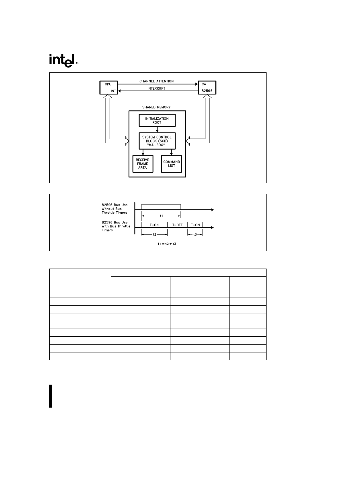
82596 AND HOST CPU INTERACTION
The 82596DX/SX and the host CPU communicate
through shared memory. Because of its on-chip
DMA capability, the 82596 can make data block
transfers (buffers and frames) independently of the
CPU; this greatly reduces the CPU byte transfer
overhead.
NOTE:
The 82596DX and 82596SX differ in their address
pin definitions and their data bus sizes. Information
in this data sheet applies to both versions unless
otherwise stated.
The 82596 is a multitasking coprocessor that comprises two independent logical unitsÐthe Command
Unit (CU) and the Receive Unit (RU). The CU executes commands from shared memory. The RU handles all activities related to frame reception. The independence of the CU and RU enables the 82596 to
engage in both activities simultaneouslyÐthe CU
can fetch and execute commands from memory
while the RU is storing received frames in memory.
The CPU is only involved with this process after the
CU has executed a sequence of commands or the
RU has finished storing a sequence of frames.
The CPU and the 82596 use the hardware signals
Interrupt (INT) and Channel Attention (CA) to initiate
communication with the System Control Block
(SCB), see Figure 4. The 82596 uses INT to alert the
CPU of a change in the contents of the SCB, the
CPU uses CA to alert the 82596.
The 82596 has a CPU Port Access state that allows
the CPU to execute certain functions without accessing memory. The 82596 PORT
pin and data bus
pins are used to enable this feature. The CPU can
directly activate four operations when the 82596 is in
this state.
#
Write an alternative System Configuration Pointer
(SCP). This can be used when the 82596 cannot
use the default SCP address space.
#
Write a different Dump Command Pointer and execute Dump. This can be used for troubleshooting No Response problems.
#
The CPU can reset the 82596 via software without disturbing the rest of the system.
#
A self-test can be used for board testing; the
82596 will execute a self-test and write the results to memory.
82596 BUS INTERFACE
The 82596DX/SX has bus interface timings and pin
definitions that are compatible with Intel’s 32-bit i386
DX and i386 SX microprocessors. This eliminates
the need for additional bus interface logic. Operating
at 33 MHz, the 82596’s bus bandwidth can be as
high as 66 MB/s. Since Ethernet only requires
1.25 MB/s, this leaves a considerable amount of
bandwidth for the CPU. The 82596 also has a bus
throttle to regulate its use of the bus. Two timers can
be programmed through the SCB: one controls the
maximum time the 82596 can remain on the bus, the
other controls the time the 82596 must stay off the
bus (see Figure 5). The bus throttle can be programmed to trigger internally with HLDA or externally with BREQ. These timers can restrict the 82596
HOLD activation time and improve bus utilization.
82596 MEMORY ADDRESSING
The 82596 has a 32-bit memory address range,
which allows addressing up to four gigabytes of
memory. The 82596 has three memory addressing
modes (see Table 1).
#
82586 Mode. The 82596 has a 24-bit memory
address range. The System Control Block, Command List, Receive Descriptor List, and Buffer
Descriptors must reside in one 64-kB memory
segment. Transmit and Receive buffers can reside in a 24-bit address space.
#
32-Bit Segmented Mode. The 82596 has a 32bit memory address range. The System Control
Block, Command List, Receive Descriptor List,
and Buffer Descriptors must reside in one 64-kB
memory segment. Transmit and Receive buffers
can reside in a 32-bit address space.
#
Linear Mode. The 82596 has a 32-bit memory
address range. Any memory structure can reside
anywhere within the 32-bit memory address
range.
14
82596DX/SX
290219– 4
Figure 4. 82596 and Host CPU Intervention
290219– 5
Figure 5. Bus Throttle Timers
Table 1. 82596 Memory Addressing Formats
Operation Mode
Pointer or Offset
82586
32-Bit
Linear
Segmented
ISCP ADDRESS 24-Bit Linear 32-Bit Linear 32-Bit Linear
SCB ADDRESS Base (24)aOffset (16) Base (32)aOffset (16) 32-Bit Linear
Command Block Pointers Base (24)aOffset (16) Base (32)aOffset (16) 32-Bit Linear
Rx Frame Descriptors Base (24)aOffset (16) Base (32)aOffset (16) 32-Bit Linear
Tx Frame Descriptors Base (24)aOffset (16) Base (32)aOffset (16) 32-Bit Linear
Rx Buffer Descriptors Base (24)aOffset (16) Base (32)aOffset (16) 32-Bit Linear
Tx Buffer Descriptors Base (24)aOffset (16) Base (32)aOffset (16) 32-Bit Linear
Rx Buffers 24-Bit Linear 32-Bit Linear 32-Bit Linear
Tx Buffers 24-Bit Linear 32-Bit Linear 32-Bit Linear
15
82596DX/SX
290219– 6
Figure 6. 82596 Shared Memory Structure
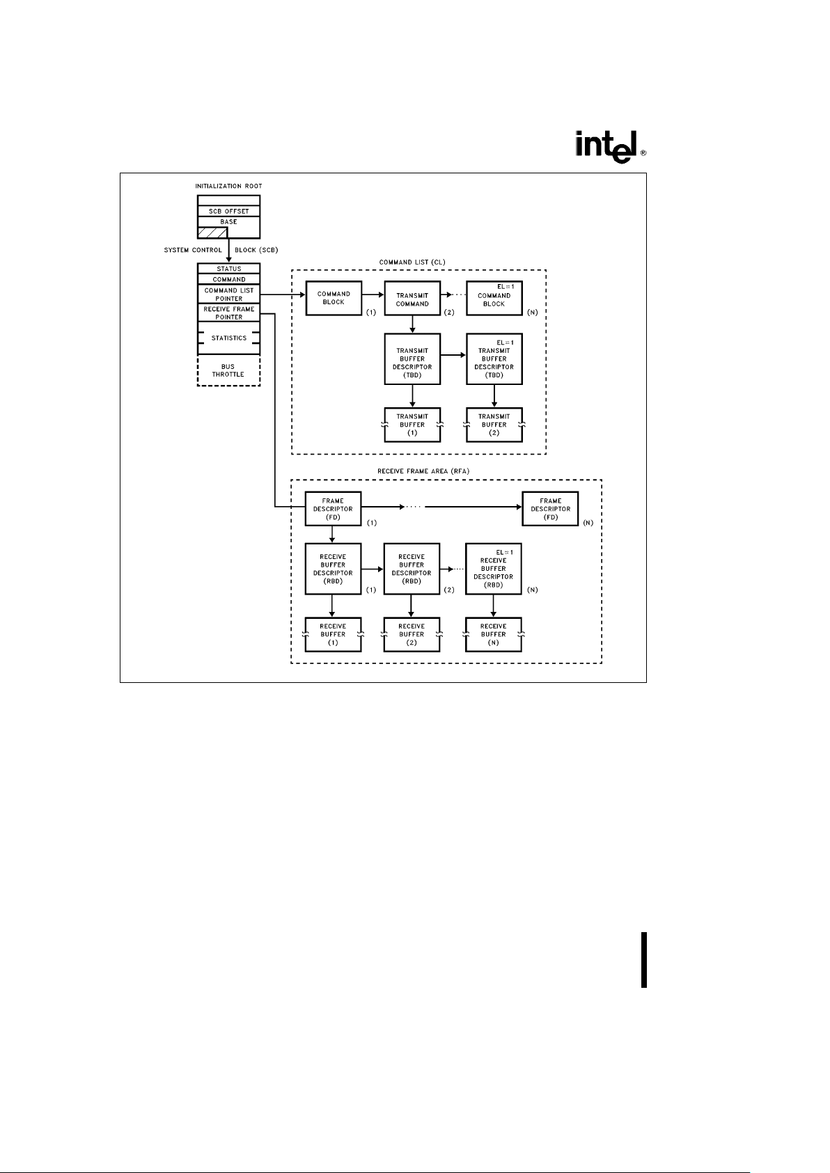
82596 SYSTEM MEMORY
STRUCTURE
The Shared Memory structure consists of four parts:
the Initialization Root, the System Control Block, the
Command List, and the Receive Frame Area (see
Figure 6).
The Initialization Root is in an established location
known to the host CPU and the 82596 (00FFFFF6h).
However, the CPU can establish the Initialization
Root in another location by using the CPU Port access. This root is accessed during initialization, and
points to the System Control Block.
The System Control Block serves as a bidirectional
mail drop for the host CPU and the 82596 CU and
RU. It is the central point through which the CPU and
the 82596 exchange control and status information.
The SCB has two areas. The first contains instructions from the CPU to the 82596. These include:
control of the CU and RU (Start, Abort, Suspend,
and Resume), a pointer to the list of CU commands,
a pointer to the Receive Frame Area, a set of Interrupt Acknowledge bits, and the T-ON and T-OFF
timers for the bus throttle. The second area contains
status information the 82596 is sending to the CPU.
Such as, the CU and RU states (Idle, Active
16

82596DX/SX
Ready, Suspended, No Receive Resources, etc.), interrupt bits (Command Completed, Frame Received,
CU Not Ready, and RU Not Ready), and statistical
counters.
The Command List functions as a program for the
CU; individual commands are placed in memory
units called Command Blocks (CBs). These CBs
contain the parameters and status of specific highlevel commands called Action Commands; e.g.,
Transmit or Configure.
Transmit causes the 82596 to transmit a frame. The
Transmit CB contains the destination address, the
length field, and a pointer to a list of linked buffers
holding the frame that is to be constructed from several buffers scattered throughout memory. The
Command Unit operates without CPU intervention;
the DMA for each buffer, and the prefetching of references to new buffers, is performed in parallel. The
CPU is notified only after a transmission is complete.
The Receive Frame Area is a list of Free Frame Descriptors (descriptors not yet used) and a list of userprepared buffers. Frames arrive at the 82596 unsolicited; the 82596 must always be ready to receive
and store them in the Free Frame Area. The Receive Unit fills the buffers when it receives frames,
and reformats the Free Buffer List into receivedframe structures. The frame structure is, for all practical purposes, identical to the format of the frame to
be transmitted. The first Frame descriptor is referenced by the SCB. Unless the 82596 is configured
to Save Bad Frames, the frame descriptor, and the
associated buffer descriptor, which is wasted when
a bad frame is received, are automatically reclaimed
and returned to the Free Buffer List.
Receive buffer chaining (storing incoming frames in
a linked buffer list) significantly improves memory
utilization. Without buffer chaining, the user must allocate consecutive blocks of memory, each capable
of containing a maximum frame (for Ethernet, 1518
bytes). Since an average frame is about 200 bytes,
this is very inefficient. With buffer chaining, the user
can allocate small buffers and the 82596 will only
use those that are needed.
Figure 7 A–D illustrates how the 82596 uses the
Receive Frame Area. Figure 7A shows an unused
Receive Frame Area composed of Free Frame Descriptors and Free Receive Buffers prepared by the
user. The SCB points to the first Frame Descriptor of
the Frame Descriptor List. Figure 7B shows the
same Receive Frame Area after receiving one
frame. This first frame occupies two Receive Buffers
and one Frame DescriptorÐa valid received frame
will only occupy one Frame Descriptor. After receiving this frame the 82596 sets the next Free Frame
Descriptor RBD pointer to the next Free RBD. Figure
7C shows the RFA after receiving a second frame.
In this example the second frame occupies only one
Receive Buffer and one RFD. The 82596 again sets
the RBD pointer. This process is repeated again in
Figure 7D, showing the reception of another frame
using one Receive Buffer; in this example there is an
extra Frame Descriptor.
TRANSMIT AND RECEIVE MEMORY
STRUCTURES
There are three memory structures for reception and
transmission. The 82586 memory structure, the
Flexible memory structure, and the Simplified memory structure. The 82586 mode is selected by configuring the 82596 during initialization. In this mode all
the 82596 memory structures are compatible with
the 82586 memory structures.
When the 82596 is not configured to the 82586
mode, the other two memory structures, Simplified
and Flexible, are available for transmitting and receiving. These structures are selected by setting the
S/F bit in the Transmit Command and/or the Receive Frame Descriptor (see Figures 29, 30, 41, and
42). It is recommended that any linked list of buffers
be relegated to a single typeÐeither simplified or
flexible. The Simplified memory structure offers a
simple structure for ease of programming (see Figure 8). All information about a frame is contained in
one structure; for example, during reception the RFD
and data field are contained in one structure.
The Flexible memory structure (see Figure 9) has a
control field that allows the programmer to specify
the amount of receive data the RFD will contain for
receive operations and the amount of transmit data
the Transmit Command Block will contain for transmit operations. For example, when the control field
in the RFD is set to 20 bytes during a reception, the
first 20 bytes of the data field are stored in the RFD
(6 Bytes of Destination Address, 6 Bytes of Source
Address, 2 Bytes of Length Field, and 6 Bytes of
Data), and the remainder of the data field is stored in
the Receive Data Buffers. This is useful for capturing
frame headers when header information is contained in the data field. The header information can
then be automatically stored in the RFD partitioned
from the Receive Data Buffer.
The control field can also be used for the Transmit
Command when the Flexible memory structure is
used. The quantity of data field bytes to be transmitted from the Transmit Command Block is specified
by the variable control field.
17

82596DX/SX
290219– 7
Figure 7. Frame Reception in the RFA
18

82596DX/SX
290219– 8
Figure 8. Simplified Memory Structure
290219– 9
Figure 9. Flexible Memory Structure
19
82596DX/SX
TRANSMITTING FRAMES
The 82596 executes high-level Action Commands
from the Command List in system memory. Action
Commands are fetched and executed in parallel with
the host CPU operation, thereby significantly improving system performance. The format of the Action
Commands is shown in Figure 10. Figure 28 shows
the 82586 mode, and Figures 29 and 30 shows the
command formats of the Linear and 32-bit Segmented modes.
A single Transmit command contains, as part of the
command-specific parameters, the destination address and length field of the transmitted frame and a
pointer to buffer area in memory containing the data
portion of the frame. The data field is contained in a
memory data structure consisting of a buffer descriptor (BD) and a data bufferÐor a linked list of
buffer descriptors and buffersÐas shown in Figure
11.
Multiple data buffers can be chained together using
the BDs. Thus, a frame with a long data field can be
transmitted using several (shorter) data buffers
chained together. This chaining technique allows the
system designer to develop efficient buffer management.
The 82596 automatically generates the preamble
(alternating 1s and 0s) and start frame delimiter,
fetches the destination address and length field from
the Transmit command, inserts its unique address
as the source address, fetches the data field specified by the Transmit command, and computes and
appends the CRC to the end of the frame (see Figure 12). In the Linear and 32-bit Segmented mode
the CRC can be optionally inserted on a frame-byframe basis by setting the NC bit in the Transmit
Command Block (see Figures 29 and 30).
The 82596 generates the standard End Of Carrier
(EOC) start and end frame delimiters. In EOC, the
start frame delimiter is 10101011 and the end frame
delimiter is indicated by the lack of a signal after the
last bit of the frame check sequence field has been
transmitted. In EOC, the 82596 can be configured to
extend short frames by adding pad bytes (7Eh) during transmission, according to the length field.
When a collision occurs, the 82596 manages the
jam, random wait, and retry processes, reinitializing
DMA pointers without CPU intervention. Multiple
frames can be sent by linking the appropriate number of Transmit commands together. This is particularly useful when transmitting a message larger than
the maximum frame size (1518 bytes for Ethernet).
290219– 10
Figure 10. Action Command Format
290219– 11
Figure 11. Data Buffer Descriptor and
Data Buffer Structure
20

82596DX/SX
START
DESTINATION SOURCE LENGTH DATA
FRAME END
PREAMBLE FRAME
ADDRESS ADDRESS FIELD FIELD
CHECK FRAME
DELIMITER SEQUENCE DELIMITER
Figure 12. Frame Format
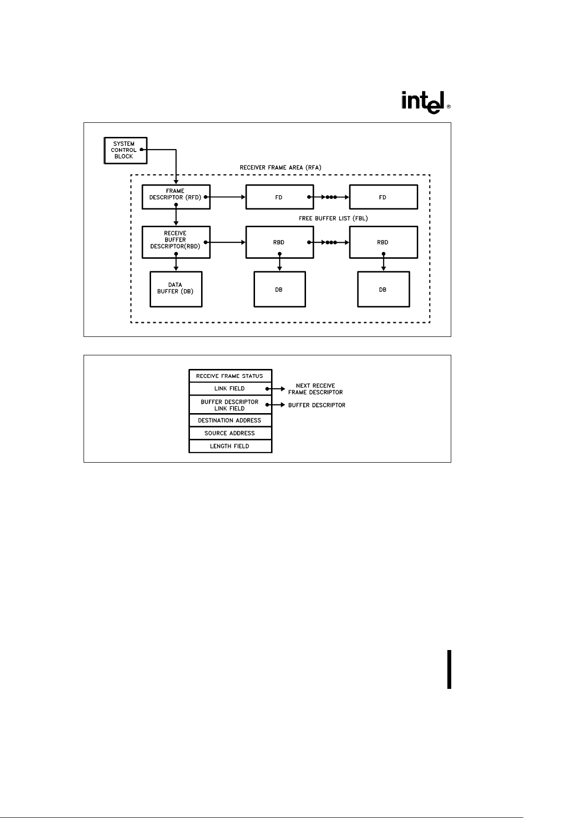
RECEIVING FRAMES
To reduce CPU overhead, the 82596 is designed to
receive frames without CPU supervision. The host
CPU first sets aside an adequate receive buffer
space and then enables the 82596 Receive Unit.
Once enabled, the RU watches for arriving frames
and automatically stores them in the Receive Frame
Area (RFA). The RFA contains Receive Frame Descriptors, Receive Buffer Descriptors, and Data Buffers (see Figure 13). The individual Receive Frame
Descriptors make up a Receive Descriptor List
(RDL) used by the 82596 to store the destination
and source addresses, the length field, and the
status of each frame received (see Figure 14).
Once enabled, the 82596 checks each passing
frame for an address match. The 82596 will recognize its own unique address, one or more multicast
addresses, or the broadcast address. If a match is
found the 82596 stores the destination and source
addresses and the length field in the next available
RFD. It then begins filling the next available Data
Buffer on the FBL, which is pointed to by the current
RFD, with the data portion of the incoming frame. As
one Data Buffer is filled, the 82596 automatically
fetches the next DB on the FBL until the entire frame
is received. This buffer chaining technique is particularly memory efficient because it allows the system
designer to set aside buffers to fit frames much
shorter than the maximum allowable frame length. If
AL-LOC
e
1, or if the flexible memory structure is
used, the addresses and length field can be placed
in the receive buffer.
Once the entire frame is received without error, the
82596 does the following housekeeping tasks.
#
The actual count field of the last Buffer Descriptor used to hold the frame just received is updated with the number of bytes stored in the associated Data Buffer.
#
The next available Receive Frame Descriptor is
fetched.
#
The address of the next available Buffer Descriptor is written to the next available Receive Frame
Descriptor.
#
A frame received interrupt status bit is posted in
the SCB.
#
An interrupt is sent to the CPU.
If a frame error occurs, for example a CRC error, the
82596 automatically reinitializes its DMA pointers
and reclaims any data buffers containing the bad
frame. The 82596 will continue to receive frames
without CPU help as long as Receive Frame Descriptors and Data Buffers are available.
82596 NETWORK MANAGEMENT
AND DIAGNOSTICS
The behavior of data communication networks is
normally very complex because of their distributed
and asynchronous nature. It is particularly difficult to
pinpoint a failure when it occurs. The 82596 has extensive diagnostic and network management functions that help improve reliability and testability. The
82596 reports on the following events after each
frame is transmitted.
#
Transmission successful.
#
Transmission unsuccessful. Lost Carrier Sense.
#
Transmission unsuccessful. Lost Clear to Send.
#
Transmission unsuccessful. A DMA underrun occurred because the system bus did not keep up
with the transmission.
#
Transmission unsuccessful. The number of collisions exceeded the maximum allowed.
#
Number of Collisions. The number of collisions
experienced during transmission of the frame.
#
Heartbeat Indicator. This indicates the presence
of a heartbeat during the last Interframe Spacing
(IFS) after transmission.
When configured to Save Bad Frames the 82596
checks each incoming frame and reports the following errors.
#
CRC error. Incorrect CRC in a properly aligned
frame.
#
Alignment error. Incorrect CRC in a misaligned
frame.
#
Frame too short. The frame is shorter than the
value configured for minimum frame length.
#
Overrun. Part of the frame was not placed in
memory because the system bus did not keep up
with incoming data.
#
Out of buffer. Part of the frame was discarded
because of insufficient memory storage space.
#
Receive collision. A collision was detected during
reception and the destination address of the incoming frame passes 82596 address filtering.
Collisions in the preamble are not counted.
#
Length error. A frame not matching the frame
length parameter was detected.
21
82596DX/SX
290219– 12
Figure 13. Receive Frame Area Diagram
290219– 13
Figure 14. Receive Frame Descriptor
22

82596DX/SX
NETWORK PLANNING AND
MAINTENANCE
To properly plan, operate, and maintain a communication network, the network management entity
must accumulate information on network behavior.
The 82596 provides a rich set of network-wide diagnostics that can serve as the basis for a network
management entity.
Information on network activity is provided in the
status of each frame transmitted. The 82596 reports
the following activity indicators after each frame.
#
Number of collisions. The number of collisions
the 82596 experienced while attempting to transmit the frame.
#
Deferred transmission. During the first transmission attempt the 82596 had to defer to traffic on
the link.
The 82596 updates its 32-bit statistical counters after each received frame that both passes address
filtering and is longer than the Minimum Frame
Length configuration parameter. The 82596 reports
the following statistics.
#
CRC errors. The number of well-aligned frames
that experienced a CRC error.
#
Alignment errors. The number of misaligned
frames that experienced a CRC error.
#
No resources. The number of frames that were
discarded because of insufficient resources for
reception.
#
Overrun errors. The number of frames that were
not completely stored in memory because the
system bus did not keep up with incoming data.
#
Receive Collision counter. The number of collisions detected during receive. Collisions occurring before the minimum frame length will be
counted as short frames. Collisions in the preamble will not be counted at all.
#
Short Frame counter. The number of frames that
were discarded because they were shorter than
the configured minimum frame length.
Once again, these counters are not updated until the
82596 decodes a destination address match.
The 82596 can be configured to Promiscuous mode.
In this mode it captures all frames transmitted on the
network without checking the Destination Address.
This is useful when implementing a monitoring station to capture all frames for analysis.
A useful method of capturing frame headers is to
use the Simplified memory mode, configure the
82596 to Save Bad Frames, and configure the
82596 to Promiscuous mode with space in the RFD
allocated for specific number of receive data bytes.
The 82596 will receive all frames and put them in the
RFD. Frames that exceed the available space in the
RFD will be truncated, the status will be updated,
and the 82596 will retrieve the next RFD. This allows
the user to capture the initial data bytes of each
frame (for instance, the header) and discard the remainder of the frame.
The 82596 also has a monitor mode for network
analysis. During normal operation the receive function enables the 82596 to receive frames which pass
address filtering. These frames must have the Start
of Frame Delimiter (SFD) field and must be longer
than the absolute minimum frame length of 5 bytes
(6 bytes in case of Multicast address filtering). Contents and status of the received frames are transferred to memory. The monitor function enables the
82596 to simply evaluate the incoming frames. The
82596 can monitor the frames that pass or do not
pass the address filtering. It can also monitor frames
which do not have the SFD fields. The 82596 can be
configured to only keep statistical information about
monitor frames. Three options are available in the
Monitor mode. These modes are selectable by the
two monitor mode configuration bits available in the
configuration command.
When the first option is selected, the 82596 receives
good frames that pass address filtering and transfers them to memory while monitoring frames that
do not pass address filtering or are shorter than the
minimum frame size (these frames are not transferred to memory). When this option is used the
82596 updates six counters: CRC errors, alignment
errors, no resource errors, overrun errors, short
frames, and total good frames received.
When the second option is selected, the receive
function is completely disabled. The 82596 monitors
only those frames that pass address filterings and
meet the minimum frame length requirement. When
this option is used the 82596 updates six counters:
CRC errors, alignment errors, total frames (good and
bad), short frames, collisions detected, and total
good frames.
When the third option is selected, the receive function is completely disabled. The 82596 monitors all
frames, including frames that do not have a Start
Frame Delimiter. When this option is used the 82596
updates six counter (CRC errors, alignment errors,
total frames (good and bad), short frames, collisions
detected, and total good frames.
23

82596DX/SX
STATION DIAGNOSTICS
AND SELF-TEST
The 82596 provides a large set of diagnostic and
network management functions. These include internal and external loopback and time domain reflectometry for locating fault points in the network cable.
The 82596 ensures software reliability by dumping
the contents of the 82596 internal registers into system memory. The 82596 has a self-test mode that
enables it to run an internal self-test and place the
results in system memory.
82586 SOFTWARE COMPATIBILITY
The 82596 has a software-compatible state in which
all its memory structures are compatible with the
82586 memory structure. This includes all the Action
Commands, the Receive Frame Area (including the
RFD, Buffer Descriptors, and Data Buffers), the System Control Block, and the initialization procedures.
There are two minor differences between the 82596
in the 82586-Compatible memory structure and the
82586.
#
When the internal and external loopback bits in
the Configure command are set to 11 the 82596
is in external loopback and the LPBK
pin is activated; in the 82586 this situation would produce
internal loopback.
#
During a Dump command both the 82596 and
82586 dump the same number of bytes; however,
the data format is different.
INITIALIZING THE 82596
A Reset command is issued to the 82596 to prepare
it for normal operation. The 82596 is initialized
through two data structures that are addressed by
two pointers, the System Configuration Pointer
(SCP) and the Intermediate System Configuration
Pointer (ISCP). The initialization procedure begins
when a Channel Attention signal is asserted after
RESET. The 82596 uses the address of the double
word that contains the SCP as a defaultÐ
00FFFFF4h. Before the CA signal is asserted this
default address can be changed to any other available address by asserting the PORT
pin and provid-
ing the desired address over the D
31–D4
pins of the
address bus. Pins D
3–D0
must be 0010; i.e., any
alternative address must be aligned to 16 byte
boundaries. All addresses sent to the 82596 must be
word aligned, which means that all pointers and
memory structures must start on an even address
(A
0
e
zero).
SYSTEM CONFIGURATION POINTER
(SCP)
The SCP contains the SYSBUS byte and the location of the next structure of the initialization process,
the ISCP. The following parameters are selected in
the SYSBUS.
#
The 82596 operation mode.
#
The Bus Throttle timer triggering method.
#
Lock enabled.
#
Interrupt polarity.
#
Big Endian 32-bit entity mode.
Byte ordering is determined by the LE/BE
pin.
LE/BE
e
1 selects little endian byte ordering and
LE/BE
e
0 selects big endian byte ordering.
NOTE:
In the following, X indicates a bit not checked in
82586 mode. This bit must be set to 0 in all other
modes.
24
 Loading...