

Intel Corporation A387DX Datasheet
*Other brands and names are the property of their respective owners.
Information in this document is provided in connection with Intel products. Intel assumes no liability whatsoever, including infringement of any patent or
copyright, for sale and use of Intel products except as provided in Intel’s Terms and Conditions of Sale for such products. Intel retains the right to make
changes to these specifications at any time, without notice. Microcomputer Products may have minor variations to this specification known as errata.
March 1992
COPYRIGHT
©
INTEL CORPORATION, 1995
Order Number: 240448-005
Intel387TMDX
MATH COPROCESSOR
Y
High Performance 80-Bit Internal
Architecture
Y
Implements ANSI/IEEE Standard 7541985 for Binary Floating-Point
Arithmetic
Y
Expands Intel386TMDX CPU Data
Types to Include 32-, 64-, 80-Bit
Floating Point, 32-, 64-Bit Integers and
18-Digit BCD Operands
Y
Directly Extends Intel386TMDX CPU
Instruction Set to Include
Trigonometric, Logarithmic,
Exponential and Arithmetic Instructions
for All Data Types
Y
Upward Object-Code Compatible from
8087 and 80287
Y
Full-Range Transcendental Operations
for SINE, COSINE, TANGENT,
ARCTANGENT and LOGARITHM
Y
Built-In Exception Handling
Y
Operates Independently of Real,
Protected and Virtual-8086 Modes of
the Intel386
TM
DX Microprocessor
Y
Eight 80-Bit Numeric Registers, Usable
as Individually Addressable General
Registers or as a Register Stack
Y
Available in 68-Pin PGA Package
Y
One Version Supports 16 MHz –33 MHz
Speeds
(See Packaging Spec: OrderÝ231369)
The Intel387TMDX Math CoProcessor (MCP) is an extension of the Intel386TMmicroprocessor architecture.
The combination of the Intel387 DX MCP with the Intel386
TM
DX Microprocessor dramatically increases the
processing speed of computer application software which utilize mathematical operations. This makes an ideal
computer workstation platform for applications such as financial modeling and spreadsheets, CAD/CAM, or
graphics.
The Intel387 DX Math CoProcessor adds over seventy mnemonics to the Intel386 DX Microprocessor instruction set. Specific Intel387 DX MCP math operations include logarithmic, arithmetic, exponential, and trigonometric functions. The Intel387 DX MCP supports integer, extended integer, floating point and BCD data
formats, and fully conforms to the ANSI/IEEE floating point standard.
The Intel387 DX Math CoProcessor is object code compatible with the Intel387 SX MCP, and upward object
code compatible from the 80287 and 8087 math coprocessors. Object code for Intel386 DX/Intel387 DX is
also compatible with the Intel486
TM
microprocessor. The Intel387 DX MCP is manufactured on 1 micron,
CHMOS IV technology and packaged in a 68-pin PGA package.
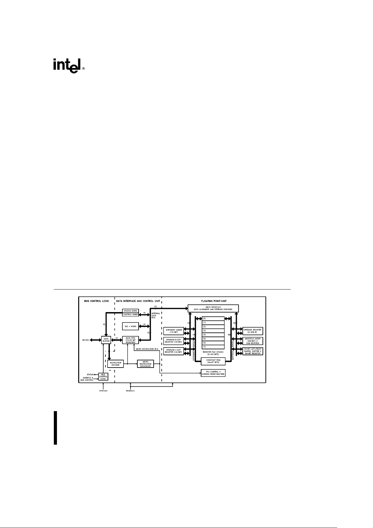
240448– 1
Figure 0.1. Intel387TMDX Math CoProcessor Block Diagram
1

Intel387TMDX Math CoProcessor
CONTENTS PAGE
1.0 FUNCTIONAL DESCRIPTION
АААААААААААААААААААААААААААААААААААААААААААААААААААААААААААА 5
2.0 PROGRAMMING INTERFACE АААААААААААААААААААААААААААААААААААААААААААААААААААААААААААА 6
2.1 Data Types ААААААААААААААААААААААААААААААААААААААААААААААААААААААААААААААААААААААААААААА 6
2.2 Numeric Operands ААААААААААААААААААААААААААААААААААААААААААААААААААААААААААААААААААААА 6
2.3 Register Set АААААААААААААААААААААААААААААААААААААААААААААААААААААААААААААААААААААААААААА 8
2.3.1 Data Registers ААААААААААААААААААААААААААААААААААААААААААААААААААААААААААААААААААААА 8
2.3.2 Tag Word АААААААААААААААААААААААААААААААААААААААААААААААААААААААААААААААААААААААААА 8
2.3.3 Status Word ААААААААААААААААААААААААААААААААААААААААААААААААААААААААААААААААААААААА 9
2.3.4 Instruction and Data Pointers ААААААААААААААААААААААААААААААААААААААААААААААААААААА 12
2.3.5 Control Word ААААААААААААААААААААААААААААААААААААААААААААААААААААААААААААААААААААА 14
2.4 Interrupt Description ААААААААААААААААААААААААААААААААААААААААААААААААААААААААААААААААААА 14
2.5 Exception Handling АААААААААААААААААААААААААААААААААААААААААААААААААААААААААААААААААААА 15
2.6 Initialization ААААААААААААААААААААААААААААААААААААААААААААААААААААААААААААААААААААААААААА 15
2.7 8087 and 80287 Compatibility ААААААААААААААААААААААААААААААААААААААААААААААААААААААААА 16
2.7.1 General Differences АААААААААААААААААААААААААААААААААААААААААААААААААААААААААААААА 16
2.7.2 Exceptions ААААААААААААААААААААААААААААААААААААААААААААААААААААААААААААААААААААААА 17
3.0 HARDWARE INTERFACE ААААААААААААААААААААААААААААААААААААААААААААААААААААААААААААААА 17
3.1 Signal Description ААААААААААААААААААААААААААААААААААААААААААААААААААААААААААААААААААААА 17
3.1.1 Intel386TMDX CPU Clock 2 (CPUCLK2) ААААААААААААААААААААААААААААААААААААААААААА 20
3.1.2 Intel387TMDX MCP Clock 2 (NUMCLK2) АААААААААААААААААААААААААААААААААААААААААА 20
3.1.3 Intel387TMDX MCP Clocking Mode (CKM) АААААААААААААААААААААААААААААААААААААААА 20
3.1.4 System Reset (RESETIN) ААААААААААААААААААААААААААААААААААААААААААААААААААААААААА 21
3.1.5 Processor Extension Request (PEREQ) ААААААААААААААААААААААААААААААААААААААААААА 21
3.1.6 Busy Status (BUSYÝ) АААААААААААААААААААААААААААААААААААААААААААААААААААААААААААА 21
3.1.7 Error Status (ERRORÝ) АААААААААААААААААААААААААААААААААААААААААААААААААААААААААА 21
3.1.8 Data Pins (D31 –D0) АААААААААААААААААААААААААААААААААААААААААААААААААААААААААААААА 21
3.1.9 Write/Read Bus Cycle (W/RÝ) ААААААААААААААААААААААААААААААААААААААААААААААААААА 21
3.1.10 Address Strobe (ADSÝ) ААААААААААААААААААААААААААААААААААААААААААААААААААААААААА 21
3.1.11 Bus Ready Input (READYÝ) ААААААААААААААААААААААААААААААААААААААААААААААААААААА 22
3.1.12 Ready Output (READYOÝ) АААААААААААААААААААААААААААААААААААААААААААААААААААААА 22
3.1.13 Status Enable (STEN) ААААААААААААААААААААААААААААААААААААААААААААААААААААААААААА 22
3.1.14 MCP SelectÝ1 (NPS1Ý) АААААААААААААААААААААААААААААААААААААААААААААААААААААААА 22
3.1.15 MCP SelectÝ2 (NPS2) АААААААААААААААААААААААААААААААААААААААААААААААААААААААААА 22
3.1.16 Command (CMD0Ý) АААААААААААААААААААААААААААААААААААААААААААААААААААААААААААА 22
2
2

CONTENTS PAGE
3.2 Processor Architecture
АААААААААААААААААААААААААААААААААААААААААААААААААААААААААААААААА 22
3.2.1 Bus Control Logic ААААААААААААААААААААААААААААААААААААААААААААААААААААААААААААААААА 23
3.2.2 Data Interface and Control Unit ААААААААААААААААААААААААААААААААААААААААААААААААААА 23
3.2.3 Floating Point Unit АААААААААААААААААААААААААААААААААААААААААААААААААААААААААААААААА 23
3.3 System Configuration АААААААААААААААААААААААААААААААААААААААААААААААААААААААААААААААААА 23
3.3.1 Bus Cycle Tracking ААААААААААААААААААААААААААААААААААААААААААААААААААААААААААААААА 24
3.3.2 MCP Addressing АААААААААААААААААААААААААААААААААААААААААААААААААААААААААААААААААА 24
3.3.3 Function Select ААААААААААААААААААААААААААААААААААААААААААААААААААААААААААААААААААА 24
3.3.4 CPU/MCP Synchronization ААААААААААААААААААААААААААААААААААААААААААААААААААААААА 24
3.3.5 Synchronous or Asynchronous Modes АААААААААААААААААААААААААААААААААААААААААААА 25
3.3.6 Automatic Bus Cycle Termination ААААААААААААААААААААААААААААААААААААААААААААААААА 25
3.4 Bus Operation ААААААААААААААААААААААААААААААААААААААААААААААААААААААААААААААААААААААААА 25
3.4.1 Nonpipelined Bus Cycles ААААААААААААААААААААААААААААААААААААААААААААААААААААААААА 26
3.4.1.1 Write Cycle АААААААААААААААААААААААААААААААААААААААААААААААААААААААААААААААААА 26
3.4.1.2 Read Cycle АААААААААААААААААААААААААААААААААААААААААААААААААААААААААААААААААА 26
3.4.2 Pipelined Bus Cycles ААААААААААААААААААААААААААААААААААААААААААААААААААААААААААААА 27
3.4.3 Bus Cycles of Mixed Type АААААААААААААААААААААААААААААААААААААААААААААААААААААААА 28
3.4.4 BUSYÝand PEREQ Timing Relationship ААААААААААААААААААААААААААААААААААААААААА 28
4.0 ELECTRICAL DATA ААААААААААААААААААААААААААААААААААААААААААААААААААААААААААААААААААААА 30
4.1 Absolute Maximum Ratings АААААААААААААААААААААААААААААААААААААААААААААААААААААААААААА 30
4.2 DC Characteristics АААААААААААААААААААААААААААААААААААААААААААААААААААААААААААААААААААА 30
4.3 AC Characteristics ААААААААААААААААААААААААААААААААААААААААААААААААААААААААААААААААААААА 31
5.0 Intel387TMDX MCP EXTENSIONS TO THE Intel386TMDX CPU INSTRUCTION
SET ААААААААААААААААААААААААААААААААААААААААААААААААААААААААААААААААААААААААААААААААААААААА 36
APPENDIX AÐCOMPATIBILITY BETWEEN THE 80287 MCP AND THE 8087 ААААААААААААА A-1
FIGURES
Figure 0.1 Intel387
TM
DX Math Coprocessor Block Diagram ААААААААААААААААААААААААААААААААААА 1
Figure 1.1 Intel386TMDX Microprocessor and Intel387TMDX Math Coprocessor Register
Set
АААААААААААААААААААААААААААААААААААААААААААААААААААААААААААААААААААААААААААААААА 5
Figure 2.1 Intel387TMDX MCP Tag Word АААААААААААААААААААААААААААААААААААААААААААААААААААААА 8
Figure 2.2 MCP Status Word АААААААААААААААААААААААААААААААААААААААААААААААААААААААААААААААААА 9
Figure 2.3 Protected Mode Intel387TMDX MCP Instruction and Data Pointer Image in
Memory, 32-Bit Format АААААААААААААААААААААААААААААААААААААААААААААААААААААААААААА 12
Figure 2.4 Real Mode Intel387TMDX MCP Instruction and Data Pointer Image in Memory, 32-
Bit Format АААААААААААААААААААААААААААААААААААААААААААААААААААААААААААААААААААААААА 13
Figure 2.5 Protected Mode Intel387TMDX MCP Instruction and Data Pointer Image in
Memory, 16-Bit Format АААААААААААААААААААААААААААААААААААААААААААААААААААААААААААА 13
Figure 2.6 Real Mode Intel387TMDX MCP Instruction and Data Pointer Image in Memory, 16-
Bit Format
АААААААААААААААААААААААААААААААААААААААААААААААААААААААААААААААААААААААА 13
Figure 2.7 Intel387TMDX MCP Control Word ААААААААААААААААААААААААААААААААААААААААААААААААА 14
Figure 3.1 Intel387TMDX MCP Pin Configuration ААААААААААААААААААААААААААААААААААААААААААААА 19
3
3

CONTENTS PAGE
FIGURES (Continued)
Figure 3.2 Asynchronous Operation
ААААААААААААААААААААААААААААААААААААААААААААААААААААААААА 20
Figure 3.3 Intel386TMDX Microprocessor and Intel387TMDX MCP Coprocessor System
Configuration АААААААААААААААААААААААААААААААААААААААААААААААААААААААААААААААААААА 23
Figure 3.4 Bus State Diagram ААААААААААААААААААААААААААААААААААААААААААААААААААААААААААААААА 25
Figure 3.5 Nonpipelined Read and Write Cycles ААААААААААААААААААААААААААААААААААААААААААААА 27
Figure 3.6 Fastest Transitions to and from Pipelined Cycles ААААААААААААААААААААААААААААААААА 28
Figure 3.7 Pipelined Cycles with Wait States АААААААААААААААААААААААААААААААААААААААААААААААА 29
Figure 3.8 STEN, BUSYÝand PEREQ Timing Relationship ААААААААААААААААААААААААААААААААА 29
Figure 4.0a Typical Output Valid Delay vs Load Capacitance at Max Operating
Temperature АААААААААААААААААААААААААААААААААААААААААААААААААААААААААААААААААААА 32
Figure 4.0b Typical Output Rise Time vs Load Capacitance at Max Operating
Temperature
АААААААААААААААААААААААААААААААААААААААААААААААААААААААААААААААААААА 32
Figure 4.1 CPUCLK2/NUMCLK2 Waveform and Measurement Points for Input/Output A.C.
Specifications
ААААААААААААААААААААААААААААААААААААААААААААААААААААААААААААААААААА 33
Figure 4.2 Output Signals ААААААААААААААААААААААААААААААААААААААААААААААААААААААААААААААААААА 33
Figure 4.3 Input and I/O Signals АААААААААААААААААААААААААААААААААААААААААААААААААААААААААААА 34
Figure 4.4 RESET Signal ААААААААААААААААААААААААААААААААААААААААААААААААААААААААААААААААААА 34
Figure 4.5 Float from STEN ААААААААААААААААААААААААААААААААААААААААААААААААААААААААААААААААА 34
Figure 4.6 Other Parameters АААААААААААААААААААААААААААААААААААААААААААААААААААААААААААААААА 35
TABLES
Table 2.1 Intel387
TM
DX MCP Data Type Representation in Memory АААААААААААААААААААААААААА 7
Table 2.2 Condition Code Interpretation ААААААААААААААААААААААААААААААААААААААААААААААААААААА 10
Table 2.3 Condition Code Interpretation after FPREM and FPREM1 Instructions ААААААААААААА 11
Table 2.4 Condition Code Resulting from Comparison ААААААААААААААААААААААААААААААААААААААА 11
Table 2.5 Condition Code Defining Operand Class АААААААААААААААААААААААААААААААААААААААААА 11
Table 2.6 Intel386TMDX Microprocessor Interrupt Vectors Reserved for MCP ААААААААААААААА 15
Table 2.7 Exceptions ААААААААААААААААААААААААААААААААААААААААААААААААААААААААААААААААААААААА 16
Table 3.1 Intel387TMDX MCP Pin Summary ААААААААААААААААААААААААААААААААААААААААААААААААА 18
Table 3.2 Intel387TMDX MCP Pin Cross-Reference ААААААААААААААААААААААААААААААААААААААААА 18
Table 3.3 Output Pin Status after Reset ААААААААААААААААААААААААААААААААААААААААААААААААААААА 21
Table 3.4 Bus Cycles Definition ААААААААААААААААААААААААААААААААААААААААААААААААААААААААААААА 24
Table 4.1 DC Specifications АААААААААААААААААААААААААААААААААААААААААААААААААААААААААААААААА 30
Table 4.2a Combinations of Bus Interface and Execution Speeds ААААААААААААААААААААААААААААА 31
Table 4.2b Timing Requirements of the Execution Unit ААААААААААААААААААААААААААААААААААААААА 31
Table 4.2c Timing Requirements of the Bus Interface Unit АААААААААААААААААААААААААААААААААААА 31
Table 4.3 Other Parameters АААААААААААААААААААААААААААААААААААААААААААААААААААААААААААААААА 35
4
4
Intel387TMDX MATH COPROCESSOR
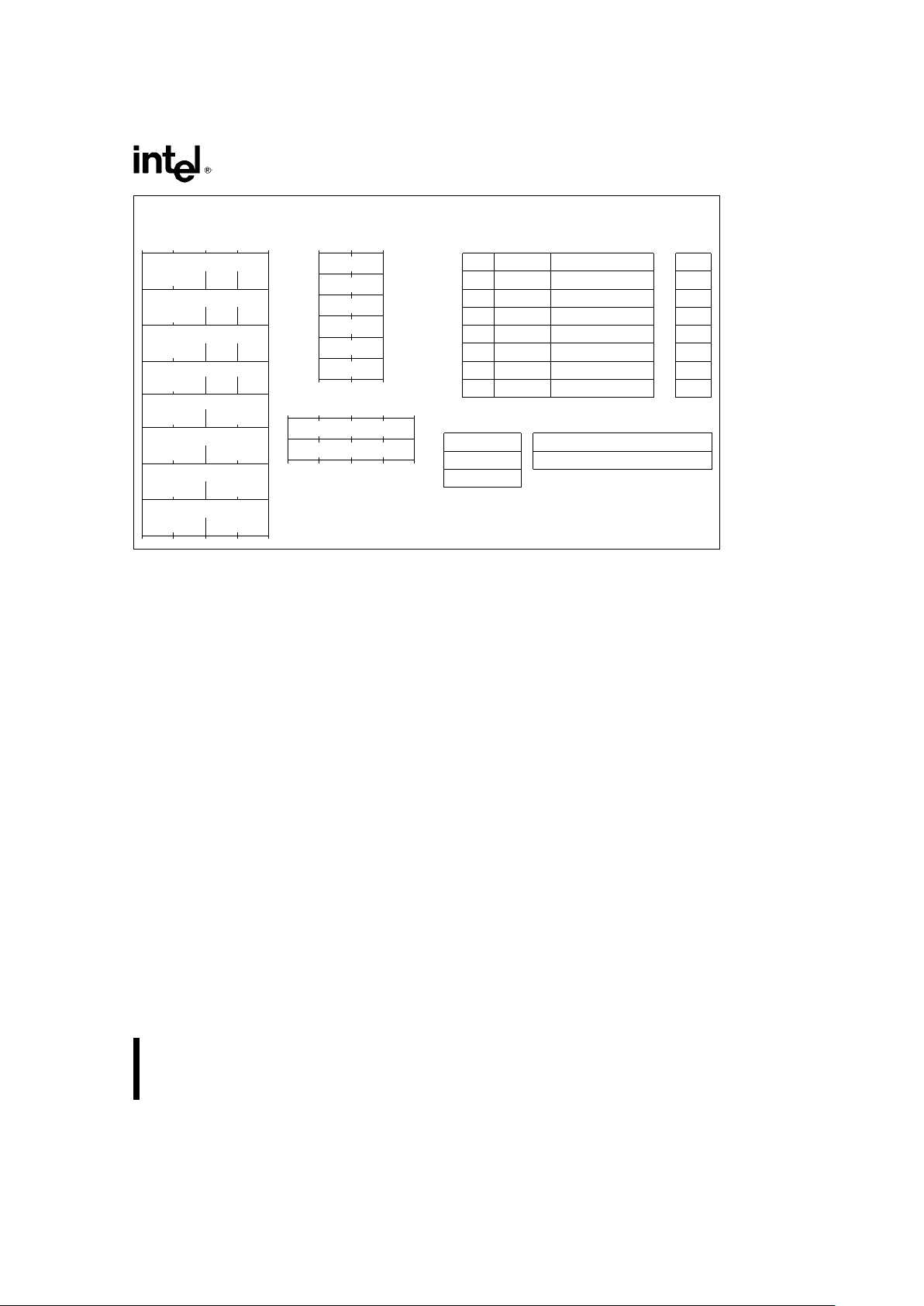
Intel386TMDX Microprocessor Registers
GENERAL REGISTERS
31 15 0
EAX
AX
AH AL
EBX
BX
BH BL
ECX
CX
CH CL
EDX
DX
DH DL
ESI SI
EDI DI
EBP BP
ESP SP
SEGMENT REGISTERS
15 0
CS
SS
DS
ES
FS
GS
31 0
EIP
EFLAGS
l
Intel387TMDX MCP Data Registers
l
Tag
Field
l
79 78 64 63 0 1 0
l
l
R0 Sign Exponent Significand
l
R1
l
R2
l
l
R3
l
R4
l
R5
l
l
R6
l
R7
l
l
l
15 0 47 0
l
Control Register Instruction Pointer (in i386TMDX CPU)
l
Status Register Data Pointer (in i386TMDX CPU)
l
l
Tag Word
l
l
l
l
l
Figure 1.1. Intel386TMDX Microprocessor and Intel387TMDX Math Coprocessor Register Set
1.0 FUNCTIONAL DESCRIPTION
The Intel387TMDX Math Coprocessor provides
arithmetic instructions for a variety of numeric data
types in Intel386
TM
DX Microprocessor systems. It
also executes numerous built-in transcendental
functions (e.g. tangent, sine, cosine, and log functions). The Intel387 DX MCP effectively extends the
register and instruction set of a Intel386 DX Microprocessor system for existing data types and adds
several new data types as well. Figure 1.1 shows the
model of registers visible to programs. Essentially,
the Intel387 DX MCP can be treated as an additional
resource or an extension to the Intel386 DX Microprocessor. The Intel386 DX Microprocessor together with a Intel387 DX MCP can be used as a single
unified system.
The Intel387 DX MCP works the same whether the
Intel386 DX Microprocessor is executing in real-address mode, protected mode, or virtual-8086 mode.
All memory access is handled by the Intel386 DX
Microprocessor; the Intel387 DX MCP merely operates on instructions and values passed to it by the
Intel386 DX Microprocessor. Therefore, the Intel387
DX MCP is not sensitive to the processing mode of
the Intel386 DX Microprocessor.
In real-address mode and virtual-8086 mode, the Intel386 DX Microprocessor and Intel387 DX MCP are
completely upward compatible with software for
8086/8087, 80286/80287 real-address mode, and
Intel386 DX Microprocessor and 80287 Coprocessor real-address mode systems.
In protected mode, the Intel386 DX Microprocessor
and Intel387 DX MCP are completely upward compatible with software for 80286/80287 protected
mode, and Intel386 DX Microprocessor and 80287
Coprocessor protected mode systems.
The only differences of operation that may appear
when 8086/8087 programs are ported to a protected-mode Intel386 DX Microprocessor and Intel387
DX MCP system (
not
using virtual-8086 mode), is in
the format of operands for the administrative instructions FLDENV, FSTENV, FRSTOR and FSAVE.
These instructions are normally used only by exception handlers and operating systems, not by applications programs.
The Intel387 DX MCP contains three functional units
that can operate in parallel to increase system performance. The Intel386 DX Microprocessor can be
transferring commands and data to the MCP
bus
control logic
for the next instruction while the MCP
floating-point unit
is performing the current numeric
instruction.
5
5

Intel387TMDX MATH COPROCESSOR
2.0 PROGRAMMING INTERFACE
The MCP adds to the Intel386 DX Microprocessor
system additional data types, registers, instructions,
and interrupts specifically designed to facilitate highspeed numerics processing. To use the MCP requires no special programming tools, because all
new instructions and data types are directly supported by the Intel386 DX CPU assembler and compilers
for high-level languages. All 8086/8088 development tools that support the 8087 can also be used
to develop software for the Intel386 DX Microprocessor and Intel387 DX Math Coprocessor in real-address mode or virtual-8086 mode. All 80286 development tools that support the 80287 can also be
used to develop software for the Intel386 DX Microprocessor and Intel387 DX Math Coprocessor.
All communication between the Intel386 DX Microprocessor and the MCP is transparent to applications software. The CPU automatically controls the
MCP whenever a numerics instruction is executed.
All physical memory and virtual memory of the CPU
are available for storage of the instructions and operands of programs that use the MCP. All memory
addressing modes, including use of displacement,
base register, index register, and scaling, are available for addressing numerics operands.
Section 6 at the end of this data sheet lists by class
the instructions that the MCP adds to the instruction
set of the Intel386 DX Microprocessor system.
2.1 Data Types
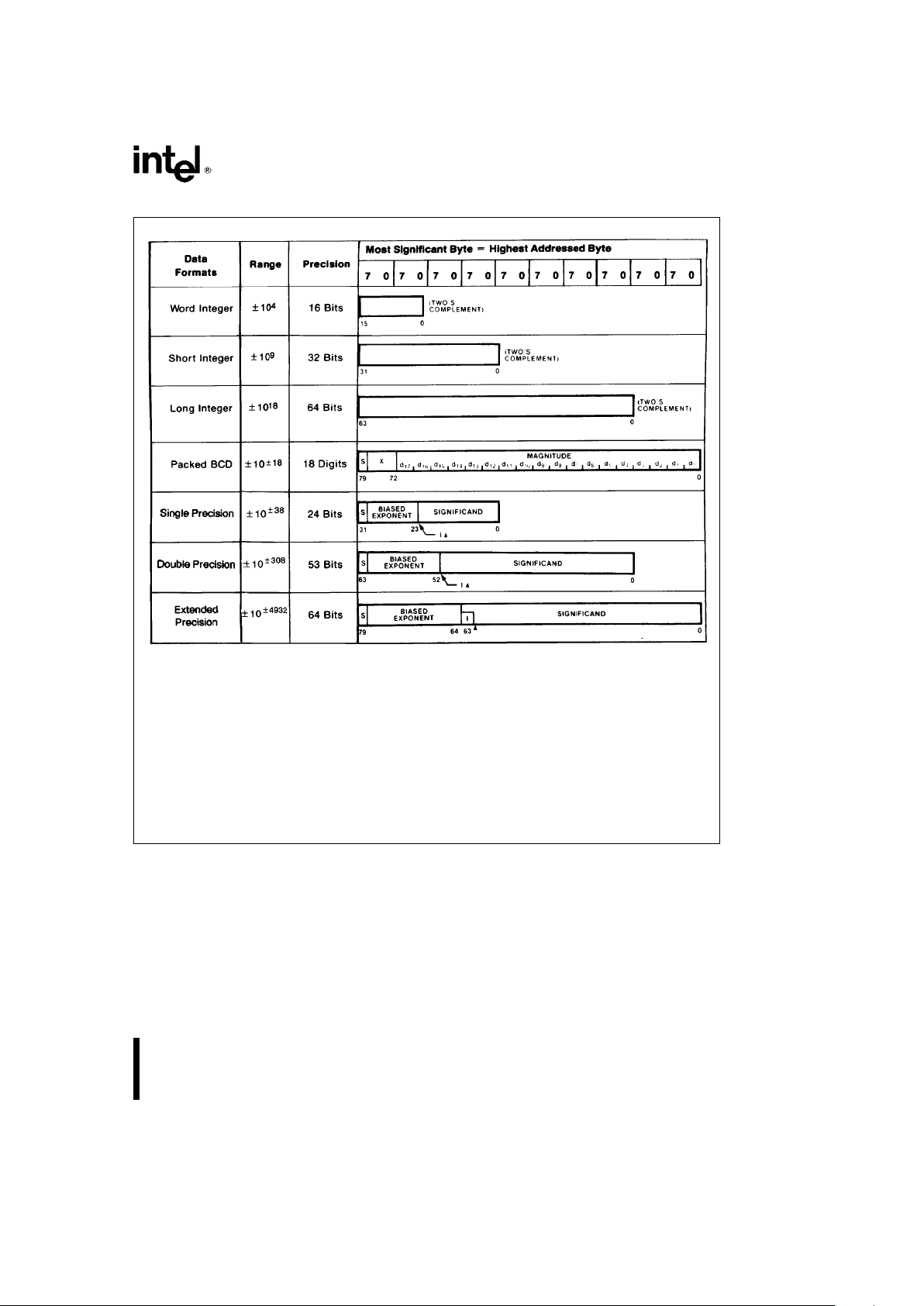
Table 2.1 lists the seven data types that the Intel387
DX MCP supports and presents the format for each
type. Operands are stored in memory with the least
significant digit at the lowest memory address. Programs retrieve these values by generating the lowest address. For maximum system performance, all
operands should start at physical-memory addresses evenly divisible by four (doubleword boundaries);
operands may begin at any other addresses, but will
require extra memory cycles to access the entire operand.
Internally, the Intel387 DX MCP holds all numbers in
the extended-precision real format. Instructions that
load operands from memory automatically convert
operands represented in memory as 16-, 32-, or 64bit integers, 32- or 64-bit floating-point numbers, or
18-digit packed BCD numbers into extended-precision real format. Instructions that store operands in
memory perform the inverse type conversion.
2.2 Numeric Operands
A typical MCP instruction accepts one or two operands and produces a single result. In two-operand
instructions, one operand is the contents of an MCP
register, while the other may be a memory location.
The operands of some instructions are predefined;
for example FSQRT always takes the square root of
the number in the top stack element.
6
6
Intel387TMDX MATH COPROCESSOR
Table 2.1. Intel387TMDX MCP Data Type Representation in Memory
240448– 2
NOTES:
(1) S
e
Sign bit (0epositive, 1enegative)
(2) d
n
e
Decimal digit (two per byte)
(3) X
e
Bits have no significance; Intel387TMDX MCP ignores when loading, zeros when storing
(4)
U
e
Position of implicit binary point
(5) I
e
Integer bit of significand; stored in temporary real, implicit in single and double precision
(6) Exponent Bias (normalized values):
Single: 127 (7FH)
Double: 1023 (3FFH)
Extended Real: 16383 (3FFFH)
(7) Packed BCD: (
b
1)S(D17...D0)
(8) Real: (
b
1)S(2
E-BIAS
)(F0F1...)
7
7

Intel387TMDX MATH COPROCESSOR
15 0
TAG (7) TAG (6) TAG (5) TAG (4) TAG (3) TAG (2) TAG (1) TAG (0)
NOTE:
The index i of tag(i) is not top-relative. A program typically uses the ‘‘top’’ field of Status Word to determine which tag(i)
field refers to logical top of stack.
TAG VALUES:
00
e
Valid
01
e
Zero
10
e
QNaN, SNaN, Infinity, Denormal and Unsupported Formats
11
e
Empty
Figure 2.1. Intel387TMDX MCP Tag Word
2.3 Register Set
Figure 1.1 shows the Intel387 DX MCP register set.
When an MCP is present in a system, programmers
may use these registers in addition to the registers
normally available on the Intel386 DX CPU.
2.3.1 DATA REGISTERS
Intel387 DX MCP computations use the MCP’s data
registers. These eight 80-bit registers provide the
equivalent capacity of twenty 32-bit registers. Each
of the eight data registers in the MCP is 80 bits wide
and is divided into ‘‘fields’’ corresponding to the
MCPs extended-precision real data type.
The Intel387 DX MCP register set can be accessed
either as a stack, with instructions operating on the
top one or two stack elements, or as a fixed register
set, with instructions operating on explicitly designated registers. The TOP field in the status word identifies the current top-of-stack register. A ‘‘push’’ operation decrements TOP by one and loads a value into
the new top register. A ‘‘pop’’ operation stores the
value from the current top register and then incre-
ments TOP by one. Like the Intel386 DX Microprocessor stacks in memory, the MCP register stack
grows ‘‘down’’ toward lower-addressed registers.
Instructions may address the data registers either
implicitly or explicitly. Many instructions operate on
the register at the TOP of the stack. These instructions implicitly address the register at which TOP
points. Other instructions allow the programmer to
explicitly specify which register to user. This explicit
register addressing is also relative to TOP.
2.3.2 TAG WORD
The tag word marks the content of each numeric
data register, as Figure 2.1 shows. Each two-bit tag
represents one of the eight numerics registers. The
principal function of the tag word is to optimize the
MCPs performance and stack handling by making it
possible to distinguish between empty and nonempty register locations. It also enables exception handlers to check the contents of a stack location without the need to perform complex decoding of the
actual data.
8
8
Intel387TMDX MATH COPROCESSOR
240448– 3
ES is set if any unmasked exception bit is set; cleared otherwise.
See Table 2.2 for interpretation of condition code.
TOP values:
000
e
Register 0 is Top of Stack
001
e
Register 1 is Top of Stack
#
#
#
111eRegister 7 is Top of Stack
For definitions of exceptions, refer to the section entitled
‘‘Exception Handling’’
Figure 2.2. MCP Status Word
2.3.3 STATUS WORD
The 16-bit status word (in the status register) shown
in Figure 2.2 reflects the overall state of the MCP. It
may be read and inspected by CPU code.
Bit 15, the B-bit (busy bit) is included for 8087 compatibility only. It reflects the contents of the ES bit
(bit 7 of the status word), not the status of the
BUSY
Ý
output of the Intel387 DX MCP.
Bits 13 –11 (TOP) point to the Intel387 DX MCP register that is the current top-of-stack.
The four numeric condition code bits (C
3–C0
) are
similar to the flags in a CPU; instructions that perform arithmetic operations update these bits to reflect the outcome. The effects of these instructions
on the condition code are summarized in Tables 2.2
through 2.5.
Bit 7 is the error summary (ES) status bit. This bit is
set if any unmasked exception bit is set; it is clear
otherwise. If this bit is set, the ERROR
Ý
signal is
asserted.
Bit 6 is the stack flag (SF). This bit is used to distinguish invalid operations due to stack overflow or underflow from other kinds of invalid operations. When
SF is set, bit 9 (C
1
) distinguishes between stack
overflow (C
1
e
1) and underflow (C
1
e
0).
Figure 2.2 shows the six exception flags in bits 5 –0
of the status word. Bits 5–0 are set to indicate that
the MCP has detected an exception while executing
an instruction. A later section entitled ‘‘Exception
Handling’’ explains how they are set and used.
Note that when a new value is loaded into the status
word by the FLDENV or FRSTOR instruction, the
value of ES (bit 7) and its reflection in the B-bit (bit
15) are not derived from the values loaded from
memory but rather are dependent upon the values of
the exception flags (bits 5 – 0) in the status word and
their corresponding masks in the control word. If ES
is set in such a case, the ERROR
Ý
output of the
MCP is activated immediately.
9
9

Intel387TMDX MATH COPROCESSOR
Table 2.2. Condition Code Interpretation
Instruction C0 (S) C3 (Z) C1 (A) C2 (C)
FPREM, FPREM1 Three least significant bits
Reduction
(see Table 2.3) of quotient
0
e
complete
Q2 Q0 Q1
1
e
incomplete
or O/U
Ý
FCOM, FCOMP,
FCOMPP, FTST, Result of comparison
Zero
Operand is not
FUCOM, FUCOMP, (see Table 2.4)
or O/U
Ý
comparable
FUCOMPP, FICOM, (Table 2.4)
FICOMP
FXAM Operand class Sign Operand class
(see Table 2.5) or O/U
Ý
(Table 2.5)
FCHS, FABS, FXCH,
FINCSTP, FDECSTP,
Zero
Constant loads, UNDEFINED UNDEFINED
FXTRACT, FLD,
or O/U
Ý
FILD, FBLD,
FSTP (ext real)
FIST, FBSTP,
FRNDINT, FST,
FSTP, FADD, FMUL,
Roundup
FDIV, FDIVR, UNDEFINED UNDEFINED
FSUB, FSUBR,
or O/U
Ý
FSCALE, FSQRT,
FPATAN, F2XM1,
FYL2X, FYL2XP1
FPTAN, FSIN Roundup Reduction
FCOS, FSINCOS UNDEFINED or O/U
Ý
,0
e
complete
undefined 1
e
incomplete
if C2
e
1
FLDENV, FRSTOR Each bit loaded from memory
FLDCW, FSTENV,
FSTCW, FSTSW, UNDEFINED
FCLEX, FINIT,
FSAVE
O/U
Ý
When both IE and SF bits of status word are set, indicating a stack exception, this bit
distinguishes between stack overflow (C1
e
1) and underflow (C1e0).
Reduction If FPREM or FPREM1 produces a remainder that is less than the modulus, reduction is
complete. When reduction is incomplete the value at the top of the stack is a partial
remainder, which can be used as input to further reduction. For FPTAN, FSIN, FCOS, and
FSINCOS, the reduction bit is set if the operand at the top of the stack is too large. In this
case the original operand remains at the top of the stack.
Roundup When the PE bit of the status word is set, this bit indicates whether the last rounding in the
instruction was upward.
UNDEFINED Do not rely on finding any specific value in these bits.
10
10

Intel387TMDX MATH COPROCESSOR
Table 2.3. Condition Code Interpretation after FPREM and FPREM1 Instructions
Condition Code
Interpretation after FPREM and FPREM1
C2 C3 C1 C0
Incomplete Reduction:
1 X X X further interation required
for complete reduction
Q1 Q0 Q2 Q MOD8
000 0
010 1
Complete Reduction:
0
100 2
C0, C3, C1 contain three least
110 3
significant bits of quotient
001 4
011 5
101 6
111 7
Table 2.4. Condition Code Resulting from Comparison
Order C3 C2 C0
TOPlOperand 0 0 0
TOP
k
Operand 0 0 1
TOP
e
Operand 1 0 0
Unordered 1 1 1
Table 2.5. Condition Code Defining Operand Class
C3 C2 C1 C0 Value at TOP
0000
a
Unsupported
0001
a
NaN
0010
b
Unsupported
0011
b
NaN
0100
a
Normal
0101
a
Infinity
0110
b
Normal
0111
b
Infinity
1000
a
0
1001
a
Empty
1010
b
0
1011
b
Empty
1100
a
Denormal
1110
b
Denormal
11
11

Intel387TMDX MATH COPROCESSOR
2.3.4 INSTRUCTION AND DATA POINTERS
Because the MCP operates in parallel with the CPU,
any errors detected by the MCP may be reported
after the CPU has executed the ESC instruction
which caused it. To allow identification of the failing
numeric instruction, the Intel386 DX Microprocessor
and Intel387 DX Math CoProcessor contains two
pointer registers that supply the address of the failing numeric instruction and the address of its numeric memory operand (if appropriate).
The instruction and data pointers are provided for
user-written error handlers. These registers are actually located in the Intel386 DX CPU, but appear to
be located in the MCP because they are accessed
by the ESC instructions FLDENV, FSTENV, FSAVE,
and FRSTOR. (In the 8086/8087 and 80286/80287,
these registers are located in the MCP.) Whenever
the Intel386 DX CPU decodes a new ESC instruction, it saves the address of the instruction (including
any prefixes that may be present), the address of
the operand (if present), and the opcode.
The instruction and data pointers appear in one of
four formats depending on the operating mode of
the Intel386 DX Microprocessor (protected mode or
real-address mode) and depending on the operandsize attribute in effect (32-bit operand or 16-bit operand). When the Intel386 DX Microprocessor is in virtual-8086 mode, the real-address mode formats are
used. (See Figures 2.3 through 2.6.) The ESC instructions FLDENV, FSTENV, FSAVE, and FRSTOR
are used to transfer these values between the Intel386 DX Microprocessor registers and memory.
Note that the value of the data pointer is
undefined
if
the prior ESC instruction did not have a memory operand.
32-BIT PROTECTED MODE FORMAT
31 23 15 7 0
RESERVED CONTROL WORD 0
RESERVED STATUS WORD 4
RESERVED TAG WORD 8
IP OFFSET C
00000 OPCODE
10..0
CS SELECTOR 10
DATA OPERAND OFFSET 14
RESERVED OPERAND SELECTOR 18
Figure 2.3. Protected Mode Intel387TMDX MCP Instruction and
Data Pointer Image in Memory, 32-Bit Format
12
12

Intel387TMDX MATH COPROCESSOR
32-BIT REAL-ADDRESS MODE FORMAT
31 23 15 7 0
RESERVED CONTROL WORD 0
RESERVED STATUS WORD 4
RESERVED TAG WORD 8
RESERVED INSTRUCTION POINTER 15..0 C
0000 INSTRUCTION POINTER 31..16 0 OPCODE 10..0 10
RESERVED OPERAND POINTER 15..0 14
0000 OPERAND POINTER 31..16 0000 00000000 18
Figure 2.4. Real Mode Intel387TMDX MCP Instruction and Data Pointer Image in Memory, 32-Bit Format
16-BIT PROTECTED MODE FORMAT
15 7 0
CONTROL WORD 0
STATUS WORD 2
TAG WORD 4
IP OFFSET 6
CS SELECTOR 8
OPERAND OFFSET A
OPERAND SELECTOR C
Figure 2.5. Protected Mode Intel387TMDX MCP
Instruction and Data Pointer
Image in Memory, 16-Bit Format
16-BIT REAL-ADDRESS MODE AND
VIRTUAL-8086 MODE FORMAT
15 7 0
CONTROL WORD 0
STATUS WORD 2
TAG WORD 4
INSTRUCTION POINTER 15..0 6
IP19.16 0 OPCODE 10..0 8
OPERAND POINTER 15..0 A
DP 19.16 00000000000 0 C
Figure 2.6. Real Mode Intel387TMDX MCP
Instruction and Data Pointer
Image in Memory, 16-Bit Format
13
13
 Loading...