Intel Corporation A376 Datasheet
*Other brands and names are the property of their respective owners.
Information in this document is provided in connection with Intel products. Intel assumes no liability whatsoever, including infringement of any patent or
copyright, for sale and use of Intel products except as provided in Intel’s Terms and Conditions of Sale for such products. Intel retains the right to make
changes to these specifications at any time, without notice. Microcomputer Products may have minor variations to this specification known as errata.
December 1990COPYRIGHT©INTEL CORPORATION, 1995 Order Number: 240182-004
376TMHIGH PERFORMANCE
32-BIT EMBEDDED PROCESSOR
Y
Full 32-Bit Internal Architecture
Ð 8-, 16-, 32-Bit Data Types
Ð 8 General Purpose 32-Bit Registers
Ð Extensive 32-Bit Instruction Set
Y
High Performance 16-Bit Data Bus
Ð 16 or 20 MHz CPU Clock
Ð Two-Clock Bus Cycles
Ð 16 Mbytes/Sec Bus Bandwidth
Y
16 Mbyte Physical Memory Size
Y
High Speed Numerics Support with the
80387SX
Y
Low System Cost with the 82370
Integrated System Peripheral
Y
On-Chip Debugging Support Including
Break Point Registers
Y
Complete Intel Development Support
Ð C, PL/M, Assembler
Ð ICE
TM
-376, In-Circuit Emulator
Ð iRMK Real Time Kernel
Ð iSDM Debug Monitor
Ð DOS Based Debug
Y
Extensive Third-Party Support:
Ð Languages: C, Pascal, FORTRAN,
BASIC and ADA*
Ð Hosts: VMS*, UNIX*, MS-DOS*, and
Others
Ð Real-Time Kernels
Y
High Speed CHMOS IV Technology
Y
Available in 100 Pin Plastic Quad FlatPack Package and 88-Pin Pin Grid Array
(See Packaging Outlines and DimensionsÝ231369)
INTRODUCTION
The 376 32-bit embedded processor is designed for high performance embedded systems. It provides the
performance benefits of a highly pipelined 32-bit internal architecture with the low system cost associated with
16-bit hardware systems. The 80376 processor is based on the 80386 and offers a high degree of compatibility with the 80386. All 80386 32-bit programs not dependent on paging can be executed on the 80376 and all
80376 programs can be executed on the 80386. All 32-bit 80386 language translators can be used for
software development. With proper support software, any 80386-based computer can be used to develop and
test 80376 programs. In addition, any 80386-based PC-AT* compatible computer can be used for hardware
prototyping for designs based on the 80376 and its companion product the 82370.
240182– 48
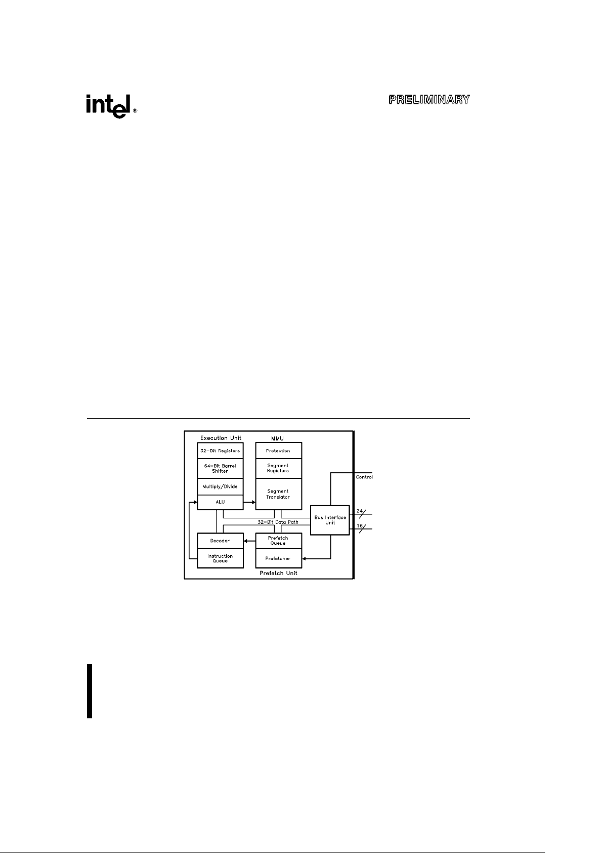
80376 Microarchitecture
Intel, iRMK, ICE, 376, 386, Intel386, iSDM, Intel1376 are trademarks of Intel Corp.
*UNIX is a registered trademark of AT&T.
ADA is a registered trademark of the U.S. Government, Ada Joint Program Office.
PC-AT is a registered trademark of IBM Corporation.
VMS is a trademark of Digital Equipment Corporation.
MS-DOS is a trademark of MicroSoft Corporation.
376 EMBEDDED PROCESSOR
1.0 PIN DESCRIPTION
240182– 52
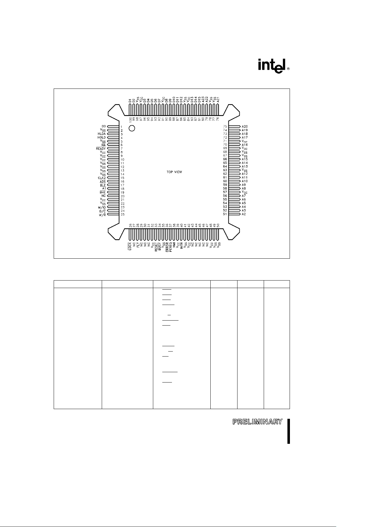
Figure 1.1. 80376 100-Pin Quad Flat-Pack Pin Out (Top View)
Table 1.1. 100-Pin Plastic Quad Flat-Pack Pin Assignments
Address Data Control N/C V
CC
V
SS
A
1
18 D
0
1 ADS 16 20 8 2
A
2
51 D
1
100 BHE 19 27 9 5
A
3
52 D
2
99 BLE 17 10 11
A
4
53 D
3
96 BUSY 34 29 21 12
A
5
54 D
4
95 CLK2 15 30 32 13
A
6
55 D
5
94 D/C 24 31 39 14
A
7
56 D
6
93 ERROR 36 43 42 22
A
8
58 D
7
92 FLT 28 44 48 35
A
9
59 D
8
90 HLDA 3 45 57 41
A
10
60 D
9
89 HOLD 4 46 69 49
A
11
61 D
10
88 INTR 40 47 71 50
A
12
62 D
11
87 LOCK 26 84 63
A
13
64 D
12
86 M/IO 23 91 67
A
14
65 D
13
83 NA 69768
A
15
66 D
14
82 NMI 38 77
A
16
70 D
15
81 PEREQ 37 78
A
17
72 READY 785
A
18
73 RESET 33 98
A
19
74 W/R 25
A
20
75
A
21
76
A
22
79
A
23
80
2
376 EMBEDDED PROCESSOR
Top View
(Component Side)
240182– 49
Bottom View
(Pin Side)
240182– 2
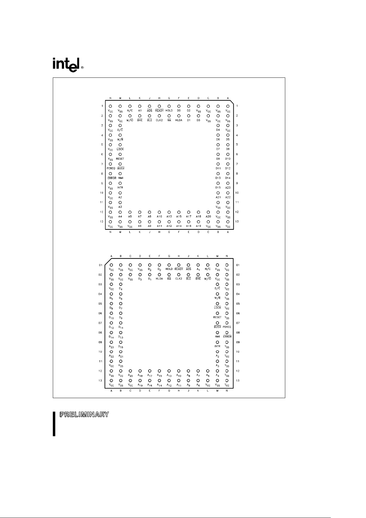
Figure 1.2. 80376 88-Pin Grid Array Pin Out
3

376 EMBEDDED PROCESSOR
Table 1.2. 88-Pin Grid Array Pin Assignments
Pin Label Pin Label Pin Label Pin Label
2H CLK2 12D A
18
2L M/IO 11A V
CC
9B D
15
12E A
17
5M LOCK 13A V
CC
8A D
14
13E A
16
1J ADS 13C V
CC
8B D
13
12F A
15
1H READY 13L V
CC
7A D
12
13F A
14
2G NA 1N V
CC
7B D
11
12G A
13
1G HOLD 13N V
CC
6A D
10
13G A
12
2F HLDA 11B V
SS
6B D
9
13H A
11
7N PEREQ 2C V
SS
5A D
8
12H A
10
7M BUSY 1D V
SS
5B D
7
13J A
9
8N ERROR 1M V
SS
4B D
6
12J A
8
9M INTR 4N V
SS
4A D
5
12K A
7
8M NMI 9N V
SS
3B D
4
13K A
6
6M RESET 11N V
SS
2D D
3
12L A
5
2B V
CC
2A V
SS
1E D
2
12M A
4
12B V
CC
12A V
SS
2E D
1
11M A
3
1C V
CC
1B V
SS
1F D
0
10M A
2
2M V
CC
13B V
SS
9A A
23
1K A
1
3N V
CC
13M V
SS
10A A
22
2J BLE 5N V
CC
2N V
SS
10B A
21
2K BHE 10N V
CC
6N V
SS
12C A
20
4M W/R 1A V
CC
12N V
SS
13D A
19
3M D/C 3A V
CC
1L N/C
4

376 EMBEDDED PROCESSOR
The following table lists a brief description of each pin on the 80376. The following definitions are used in
these descriptions:
The named signal is active LOW.
I Input signal.
O Output signal.
I/O Input and Output signal.
Ð No electrical connection.
Symbol Type Name and Function
CLK2 I CLK2 provides the fundamental timing for the 80376. For additional
information see Clock in Section 4.1.
RESET I RESET suspends any operation in progress and places the 80376 in a
known reset state. See Interrupt Signals in Section 4.1 for additional
information.
D15–D
0
I/O DATA BUS inputs data during memory, I/O and interrupt acknowledge
read cycles and outputs data during memory and I/O write cycles. See
Data Bus in Section 4.1 for additional information.
A23–A
1
O ADDRESS BUS outputs physical memory or port I/O addresses. See
Address Bus in Section 4.1 for additional information.
W/R O WRITE/READ is a bus cycle definition pin that distinguishes write
cycles from read cycles. See Bus Cycle Definition Signals in Section
4.1 for additional information.
D/C O DATA/CONTROL is a bus cycle definition pin that distinguishes data
cycles, either memory or I/O, from control cycles which are: interrupt
acknowledge, halt, and instruction fetching. See Bus Cycle Definition
Signals in Section 4.1 for additional information.
M/IO O MEMORY I/O is a bus cycle definition pin that distinguishes memory
cycles from input/output cycles. See Bus Cycle Definition Signals in
Section 4.1 for additional information.
LOCK O BUS LOCK is a bus cycle definition pin that indicates that other
system bus masters are denied access to the system bus while it is
active. See Bus Cycle Definition Signals in Section 4.1 for additional
information.
ADS O ADDRESS STATUS indicates that a valid bus cycle definition and
address (W/R
, D/C, M/IO, BHE, BLE and A23–A1) are being driven at
the 80376 pins. See Bus Control Signals in Section 4.1 for additional
information.
NA I NEXT ADDRESS is used to request address pipelining. See Bus
Control Signals in Section 4.1 for additional information.
READY I BUS READY terminates the bus cycle. See Bus Control Signals in
Section 4.1 for additional information.
BHE, BLE O BYTE ENABLES indicate which data bytes of the data bus take part in
a bus cycle. See Address Bus in Section 4.1 for additional
information.
HOLD I BUS HOLD REQUEST input allows another bus master to request
control of the local bus. See Bus Arbitration Signals in Section 4.1
for additional information.
5

376 EMBEDDED PROCESSOR
Symbol Type Name and Function
HLDA O BUS HOLD ACKNOWLEDGE output indicates that the 80376 has
surrendered control of its local bus to another bus master. See Bus
Arbitration Signals in Section 4.1 for additional information.
INTR I INTERRUPT REQUEST is a maskable input that signals the 80376 to
suspend execution of the current program and execute an interrupt
acknowledge function. See Interrupt Signals in Section 4.1 for
additional information.
NMI I NON-MASKABLE INTERRUPT REQUEST is a non-maskable input
that signals the 80376 to suspend execution of the current program
and execute an interrupt acknowledge function. See Interrupt Signals
in Section 4.1 for additional information.
BUSY I BUSY signals a busy condition from a processor extension. See
Coprocessor Interface Signals in Section 4.1 for additional
information.
ERROR I ERROR signals an error condition from a processor extension. See
Coprocessor Interface Signals in Section 4.1 for additional
information.
PEREQ I PROCESSOR EXTENSION REQUEST indicates that the processor
extension has data to be transferred by the 80376. See Coprocessor
Interface Signals in Section 4.1 for additional information.
FLT I FLOAT, when active, forces all bidirectional and output signals,
including HLDA, to the float condition. FLOAT is not available on the
PGA package. See Float for additional information.
N/C Ð NO CONNECT should always remain unconnected. Connection of a
N/C pin may cause the processor to malfunction or be incompatible
with future steppings of the 80376.
V
CC
I SYSTEM POWER provides thea5V nominal D.C. supply input.
V
SS
I SYSTEM GROUND provides 0V connection from which all inputs and
outputs are measured.
2.0 ARCHITECTURE OVERVIEW
The 80376 supports the protection mechanisms
needed by sophisticated multitasking embedded
systems and real-time operating systems. The use
of these protection mechanisms is completely optional. For embedded applications not needing protection, the 80376 can easily be configured to provide a 16 Mbyte physical address space.
Instruction pipelining, high bus bandwidth, and a
very high performance ALU ensure short average
instruction execution times and high system
throughput. The 80376 is capable of execution at
sustained rates of 2.5 –3.0 million instructions per
second.
The 80376 offers on-chip testability and debugging
features. Four break point registers allow conditional
or unconditional break point traps on code execution
or data accesses for powerful debugging of even
ROM based systems. Other testability features include self-test and tri-stating of output buffers during
RESET.
The Intel 80376 embedded processor consists of a
central processing unit, a memory management unit
and a bus interface. The central processing unit con-
sists of the execution unit and instruction unit. The
execution unit contains the eight 32-bit general registers which are used for both address calculation
and data operations and a 64-bit barrel shifter used
to speed shift, rotate, multiply, and divide operations.
The instruction unit decodes the instruction opcodes
and stores them in the decoded instruction queue
for immediate use by the execution unit.
The Memory Management Unit (MMU) consists of a
segmentation and protection unit. Segmentation allows the managing of the logical address space by
providing an extra addressing component, one that
allows easy code and data relocatability, and efficient sharing.
The protection unit provides four levels of protection
for isolating and protecting applications and the operating system from each other. The hardware enforced protection allows the design of systems with
a high degree of integrity and simplifies debugging.
Finally, to facilitate high performance system hardware designs, the 80376 bus interface offers address pipelining and direct Byte Enable signals for
each byte of the data bus.
6
376 EMBEDDED PROCESSOR
2.1 Register Set
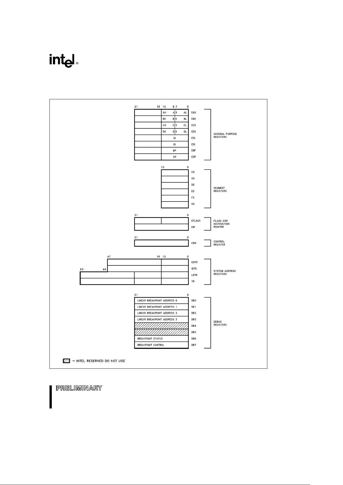
The 80376 has twenty-nine registers as shown in Figure 2.1. These registers are grouped into the following six
categories:
240182– 47
240182– 5
Figure 2.1. 80376 Base Architecture Registers
7
376 EMBEDDED PROCESSOR
General Registers: The eight 32-bit general pur-
pose registers are used to contain arithmetic and
logical operands. Four of these (EAX, EBX, ECX and
EDX) can be used either in their entirety as 32-bit
registers, as 16-bit registers, or split into pairs of
separate 8-bit registers.
Segment Registers: Six 16-bit special purpose registers select, at any given time, the segments of
memory that are immediately addressable for code,
stack, and data.
Flags and Instruction Pointer Registers: These
two 32-bit special purpose registers in Figure 2.1
record or control certain aspects of the 80376 processor state. The EFLAGS register includes status
and control bits that are used to reflect the outcome
of many instructions and modify the semantics of
some instructions. The Instruction Pointer, called
EIP, is 32 bits wide. The Instruction Pointer controls
instruction fetching and the processor automatically
increments it after executing an instruction.
Control Register: The 32-bit control register, CR0,
is used to control Coprocessor Emulation.
System Address Registers: These four special
registers reference the tables or segments supported by the 80376/80386 protection model. These tables or segments are:
GDTR (Global Descriptor Table Register),
IDTR (Interrupt Descriptor Table Register),
LDTR (Local Descriptor Table Register),
TR (Task State Segment Register).
Debug Registers: The six programmer accessible
debug registers provide on-chip support for debugging. The use of the debug registers is described in
Section 2.11 Debugging Support.
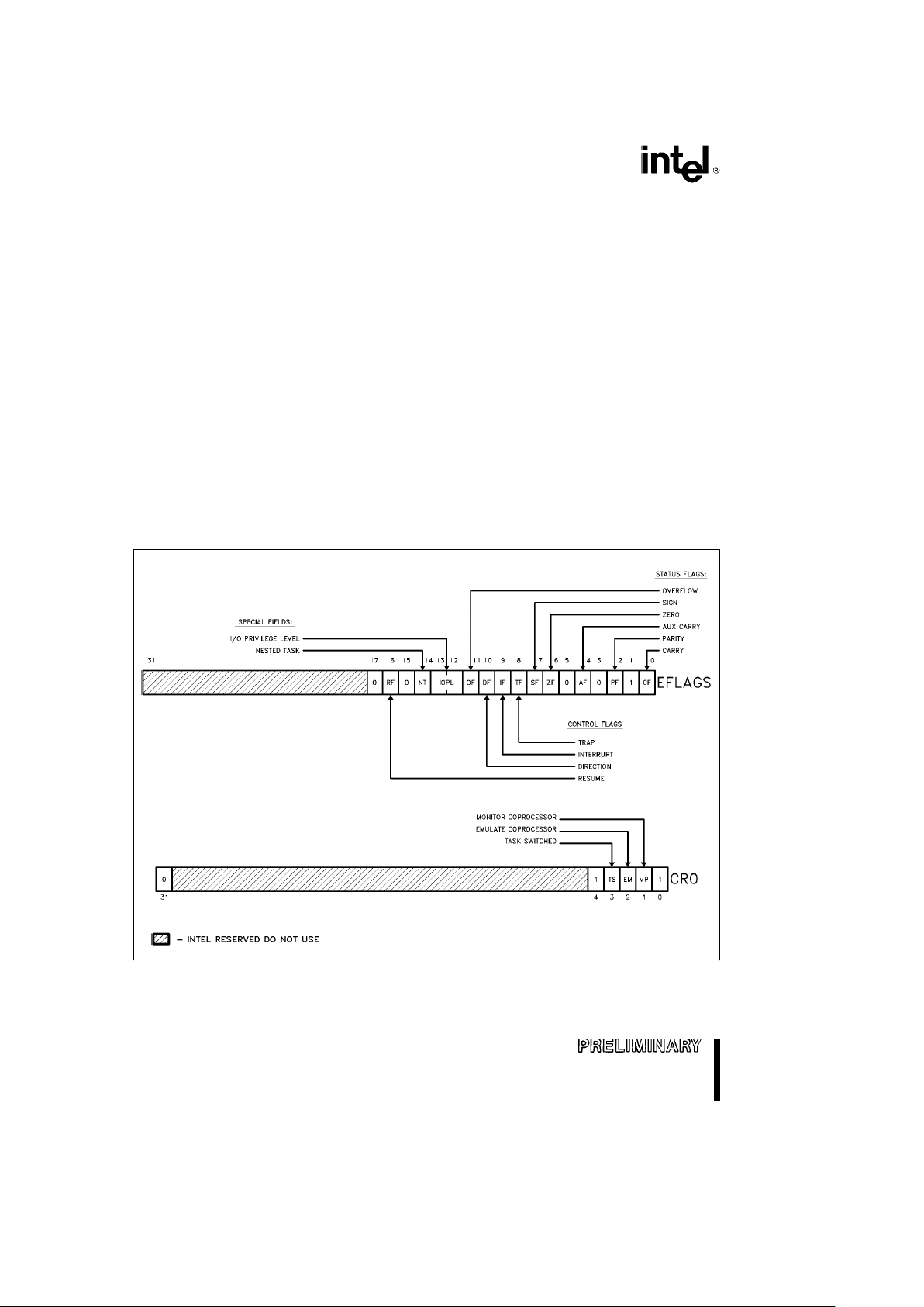
EFLAGS REGISTER
The flag Register is a 32-bit register named
EFLAGS. The defined bits and bit fields within
EFLAGS, shown in Figure 2.2, control certain operations and indicate the status of the 80376 processor.
The function of the flag bits is given in Table 2.1.
240182– 3
240182– 4
240182– 5
Figure 2.2. Status and Control Register Bit Functions
8

376 EMBEDDED PROCESSOR
Table 2.1. Flag Definitions
Bit Position Name Function
0CFCarry FlagÐSet on high-order bit carry or borrow; cleared otherwise.
2PFParity FlagÐSet if low-order 8 bits of result contain an even number
of 1-bits; cleared otherwise.
4AFAuxiliary Carry FlagÐSet on carry from or borrow to the low order
four bits of AL; cleared otherwise.
6ZFZero FlagÐSet if result is zero; cleared otherwise.
7SFSign FlagÐSet equal to high-order bit of result (0 if positive, 1 if
negative).
8TFSingle Step FlagÐOnce set, a single step interrupt occurs after the
next instruction executes. TF is cleared by the single step interrupt.
9IFInterrupt-Enable FlagÐWhen set, external interrupts signaled on the
INTR pin will cause the CPU to transfer control to an interrupt vector
specified location.
10 DF Direction FlagÐCauses string instructions to auto-increment (default)
the appropriate index registers when cleared. Setting DF causes auto-
decrement.
11 OF Overflow FlagÐSet if the operation resulted in a carry/borrow into
the sign bit (high-order bit) of the result but did not result in a
carry/borrow out of the high-order bit or vice-versa.
12, 13 IOPL I/O Privilege LevelÐIndicates the maximum CPL permitted to
execute I/O instructions without generating an exception 13 fault or
consulting the I/O permission bit map. It also indicates the maximum
CPL value allowing alteration of the IF bit.
14 NT Nested TaskÐIndicates that the execution of the current task is
nested within another task (see Task Switching).
16 RF Resume FlagÐUsed in conjunction with debug register breakpoints. It
is checked at instruction boundaries before breakpoint processing. If
set, any debug fault is ignored on the next instruction. It is reset at the
successful completion of any instruction except IRET, POPF, and
those instructions causing task switches.
CONTROL REGISTER
The 80376 has a 32-bit control register called CR0 that is used to control coprocessor emulation. This register
is shown in Figures, 2.1 and 2.2. The defined CR0 bits are described in Table 2.2. Bits 0, 4 and 31 of CR0 have
fixed values in the 80376. These values cannot be changed. Programs that load CR0 should always load bits
0, 4 and 31 with values previously there to be compatible with the 80386.
Table 2.2. CR0 Definitions
Bit Position Name Function
1MPMonitor Coprocessor ExtensionÐAllows WAIT instructions to cause
a processor extension not present exception (number 7).
2EMEmulate Processor ExtensionÐWhen set, this bit causes a
processor extension not present exception (number 7) on ESC
instructions to allow processor extension emulation.
3TSTask SwitchedÐWhen set, this bit indicates the next instruction using
a processor extension will cause exception 7, allowing software to test
whether the current processor extension context belongs to the
current task (see Task Switching).
9

376 EMBEDDED PROCESSOR
2.2 Instruction Set
The instruction set is divided into nine categories of
operations:
Data Transfer
Arithmetic
Shift/Rotate
String Manipulation
Bit Manipulation
Control Transfer
High Level Language Support
Operating System Support
Processor Control
These 80376 processor instructions are listed in Table 8.1 80376 Instruction Set and Clock Count
Summary.
All 80376 processor instructions operate on either 0,
1, 2 or 3 operands; an operand resides in a register,
in the instruction itself, or in memory. Most zero operand instructions (e.g. CLI, STI) take only one byte.
One operand instructions generally are two bytes
long. The average instruction is 3.2 bytes long.
Since the 80376 has a 16-byte prefetch instruction
queue an average of 5 instructions can be prefetched. The use of two operands permits the following types of common instructions:
Register to Register
Memory to Register
Immediate to Register
Memory to Memory
Register to Memory
Immediate to Memory
The operands are either 8-, 16- or 32-bit long.
2.3 Memory Organization
Memory on the 80376 is divided into 8-bit quantities
(bytes), 16-bit quantities (words), and 32-bit quantities (dwords). Words are stored in two consecutive
bytes in memory with the low-order byte at the lowest address. Dwords are stored in four consecutive
bytes in memory with the low-order byte at the lowest address. The address of a word or Dword is the
byte address of the low-order byte. For maximum
performance word and dword values should be at
even physical addresses.
In addition to these basic data types the 80376 processor supports segments. Memory can be divided
up into one or more variable length segments, which
can be shared between programs.
ADDRESS SPACES
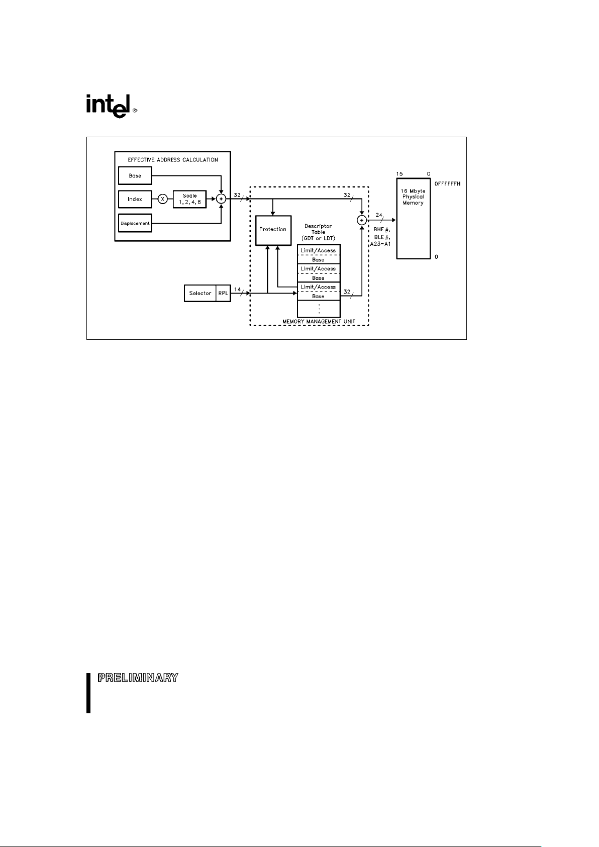
The 80376 has three types of address spaces: logical, linear, and physical. A logical address (also
known as a virtual address) consists of a selector
and an offset. A selector is the contents of a segment register. An offset is formed by summing all of
the addressing components (BASE, INDEX, and
DISPLACEMENT), discussed in Section 2.4 Ad-
dressing Modes, into an effective address.
Every selector has a logical base address associated with it that can be up to 32 bits in length. This 32bit logical base address is added to either a 32-bit
offset address or a 16-bit offset address (by using
the
address length prefix
)to form a final 32-bit lin-
ear address. This final linear address is then trun-
cated so that only the lower 24 bits of this address
are used to address the 16 Mbytes physical memory
address space. The logical base address is stored
in one of two operating system tables (i.e. the Local
Descriptor Table or Global Descriptor Table).
Figure 2.3 shows the relationship between the various address spaces.
10
376 EMBEDDED PROCESSOR
240182– 6
Figure 2.3. Address Translation
SEGMENT REGISTER USAGE
The main data structure used to organize memory is
the segment. On the 80376, segments are variable
sized blocks of linear addresses which have certain
attributes associated with them. There are two main
types of segments, code and data. The simplest use
of segments is to have one code and data segment.
Each segment is 16 Mbytes in size overlapping each
other. This allows code and data to be directly addressed by the same offset.
In order to provide compact instruction encoding
and increase processor performance, instructions
do not need to explicitly specify which segment reg-
ister is used. The segment register is automatically
chosen according to the rules of Table 2.3 (Segment
Register Selection Rules). In general, data references use the selector contained in the DS register,
stack references use the SS register and instruction
fetches use the CS register. The contents of the Instruction Pointer provide the offset. Special segment
override prefixes allow the explicit use of a given
segment register, and override the implicit rules listed in Table 2.3. The override prefixes also allow the
use of the ES, FS and GS segment registers.
There are no restrictions regarding the overlapping
of the base addresses of any segments. Thus, all 6
segments could have the base address set to zero.
Further details of segmentation are discussed in
Section 3.0 Architecture.
11

376 EMBEDDED PROCESSOR
Table 2.3. Segment Register Selection Rules
Type of Implied (Default) Segment Override
Memory Reference Segment Use Prefixes Possible
Code Fetch CS None
Destination of PUSH, PUSHF, INT,
SS None
CALL, PUSHA Instructions
Source of POP, POPA, POPF, IRET,
SS None
RET Instructions
Destination of STOS,
MOVS, REP STOS,
ES None
REP MOVS Instructions
(DI is Base Register)
Other Data References,
with Effective Address
Using Base Register of:
[
EAX
]
DS CS, SS, ES, FS, GS
[
EBX
]
DS CS, SS, ES, FS, GS
[
ECX
]
DS CS, SS, ES, FS, GS
[
EDX
]
DS CS, SS, ES, FS, GS
[
ESI
]
DS CS, SS, ES, FS, GS
[
EDI
]
DS CS, SS, ES, FS, GS
[
EBP
]
SS CS, SS, ES, FS, GS
[
ESP
]
SS CS, SS, ES, FS, GS
2.4 Addressing Modes
The 80376 provides a total of 8 addressing modes
for instructions to specify operands. The addressing
modes are optimized to allow the efficient execution
of high level languages such as C and FORTRAN,
and they cover the vast majority of data references
needed by high-level languages.
Two of the addressing modes provide for instructions that operate on register or immediate operands:
Register Operand Mode: The operand is located in
one of the 8-, 16- or 32-bit general registers.
Immediate Operand Mode: The operand is included in the instruction as part of the opcode.
The remaining 6 modes provide a mechanism for
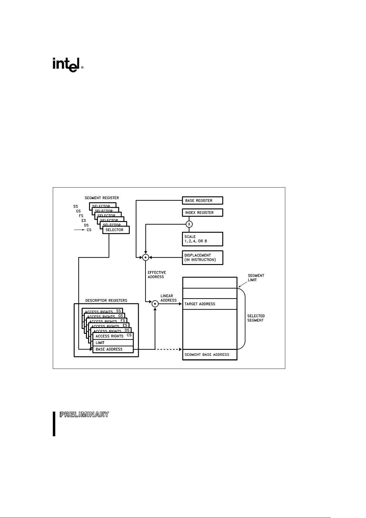
specifying the effective address of an operand. The
linear address consists of two components: the seg-
ment base address and an effective address. The
effective address is calculated by summing any
combination of the following three address elements
(see Figure 2.3):
DISPLACEMENT: an 8-, 16- or 32-bit immediate value following the instruction.
BASE: The contents of any general purpose register. The base registers are generally used by compilers to point to the start of the local variable area.
Note that if the
Address Length Prefix
is used, only
BX and BP can be used as a BASE register.
INDEX: The contents of any general purpose register except for ESP. The index registers are used to
access the elements of an array, or a string of characters. The index register’s value can be multiplied
by a scale factor, either 1, 2, 4 or 8. The scaled index
is especially useful for accessing arrays or structures. Note that if the
Address Length Prefix
is
used, no Scaling is available and only the registers
SI and DI can be used to INDEX.
12
376 EMBEDDED PROCESSOR
Combinations of these 3 components make up the 6
additional addressing modes. There is no performance penalty for using any of these addressing combinations, since the effective address calculation is
pipelined with the execution of other instructions.
The one exception is the simultaneous use of BASE
and INDEX components which requires one additional clock.
As shown in Figure 2.4, the effective address (EA) of
an operand is calculated according to the following
formula:
EA
e
BASE
Register
a
(INDEX
Register
c
scaling)
a
DISPLACEMENT
1. Direct Mode: The operand’s offset is contained
as part of the instruction as an 8-, 16- or 32-bit
DISPLACEMENT.
2. Register Indirect Mode: A BASE register contains the address of the operand.
3. Based Mode: A BASE register’s contents is added to a DISPLACEMENT to form the operand’s
offset.
4. Scaled Index Mode: An INDEX register’s contents is multiplied by a SCALING factor which is
added to a DISPLACEMENT to form the operand’s offset.
5. Based Scaled Index Mode: The contents of an
INDEX register is multiplied by a SCALING factor
and the result is added to the contents of a BASE
register to obtain the operand’s offset.
6. Based Scaled Index Mode with Displacement:
The contents of an INDEX register are multiplied
by a SCALING factor, and the result is added to
the contents of a BASE register and a DISPLACEMENT to form the operand’s offset.
240182– 7
Figure 2.4. Addressing Mode Calculations
13

376 EMBEDDED PROCESSOR
GENERATING 16-BIT ADDRESSES
The 80376 executes code with a default length for
operands and addresses of 32 bits. The 80376 is
also able to execute operands and addresses of 16
bits. This is specified through the use of override
prefixes. Two prefixes, the Operand Length Prefix
and the Address Length Prefix, override the default 32-bit length on an individual instruction basis.
These prefixes are automatically added by assem-
blers. The Operand Length and Address Length Prefixes can be applied separately or in combination to
any instruction.
The 80376 normally executes 32-bit code and uses
either 8- or 32-bit displacements, and any register
can be used as based or index registers. When executing 16-bit code (by prefix overrides), the displacements are either 8 or 16 bits, and the base and index
register conform to the 16-bit model. Table 2.4 illustrates the differences.
Table 2.4. BASE and INDEX Registers for 16- and 32-Bit Addresses
16-Bit Addressing 32-Bit Addressing
BASE REGISTER BX, BP Any 32-Bit GP Register
INDEX REGISTER SI, DI Any 32-Bit GP Register
except ESP
SCALE FACTOR None 1, 2, 4, 8
DISPLACMENT 0, 8, 16 Bits 0, 8, 32 Bits
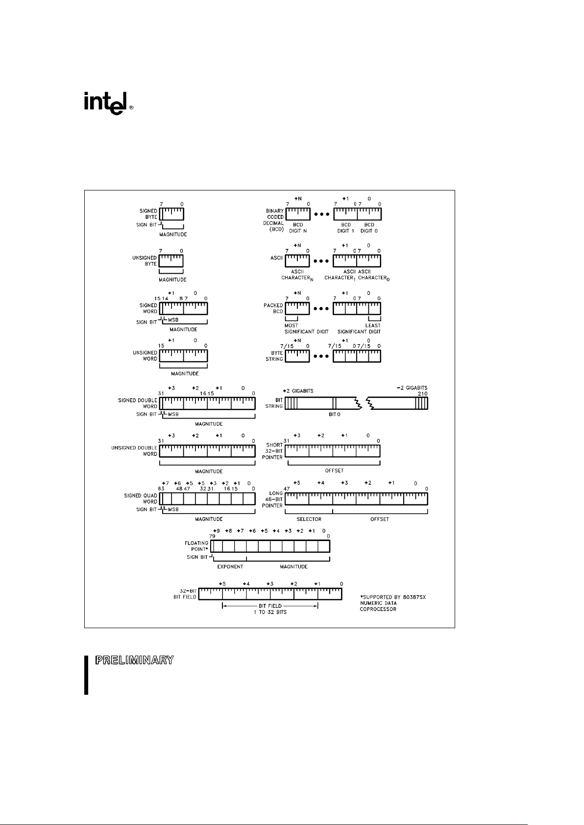
2.5 Data Types
The 80376 supports all of the data types commonly used in high level languages:
Bit: A single bit quantity.
Bit Field: A group of up to 32 contiguous bits, which spans a maximum of four
bytes.
Bit String: A set of contiguous bits, on the 80376 bit strings can be up to 16 Mbits
long.
Byte: A signed 8-bit quantity.
Unsigned Byte: An unsigned 8-bit quantity.
Integer (Word): A signed 16-bit quantity.
Long Integer (Double Word): A signed 32-bit quantity. All operations assume a 2’s complement
representation.
Unsigned Integer (Word): An unsigned 16-bit quantity.
Unsigned Long Integer
(Double Word): An unsigned 32-bit quantity.
Signed Quad Word: A signed 64-bit quantity.
Unsigned Quad Word: An unsigned 64-bit quantity.
Pointer: A 16- or 32-bit offset only quantity which indirectly references another
memory location.
Long Pointer: A full pointer which consists of a 16-bit segment selector and either a
16- or 32-bit offset.
Char: A byte representation of an ASCII Alphanumeric or control character.
String: A contiguous sequence of bytes, words or dwords. A string may
contain between 1 byte and 16 Mbytes.
BCD: A byte (unpacked) representation of decimal digits 0–9.
Packed BCD: A byte (packed) representation of two decimal digits 0 – 9 storing one
digit in each nibble.
14
376 EMBEDDED PROCESSOR
When the 80376 is coupled with a numerics Coprocessor such as the 80387SX then the following
common Floating Point types are supported.
Floating Point: A signed 32-, 64- or 80-bit real number representation. Floating point
numbers are supported by the 80387SX numerics coprocessor.
Figure 2.5 illustrates the data types supported by the 80376 processor and the 80387SX coprocessor.
240182– 8
Figure 2.5. 80376 Supported Data Types
15

376 EMBEDDED PROCESSOR
2.6 I/O Space
The 80376 has two distinct physical address
spaces: physical memory and I/O. Generally, peripherals are placed in I/O space although the
80376 also supports memory-mapped peripherals.
The I/O space consists of 64 Kbytes which can be
divided into 64K 8-bit ports, 32K 16-bit ports, or any
combination of ports which add to no more than 64
Kbytes. The M/IO
pin acts as an additional address
line, thus allowing the system designer to easily determine which address space the processor is accessing. Note that the I/O address refers to a physical address.
The I/O ports are accessed by the IN and OUT instructions, with the port address supplied as an immediate 8-bit constant in the instruction or in the DX
register. All 8-bit and 16-bit port addresses are zero
extended on the upper address lines. The I/O instructions cause the M/IO
pin to be driven LOW. I/O
port addresses 00F8H through 00FFH are reserved
for use by Intel.
2.7 Interrupts and Exceptions
Interrupts and exceptions alter the normal program
flow in order to handle external events, report errors
or exceptional conditons. The difference between interrupts and exceptions is that interrupts are used to
handle asynchronous external events while exceptions handle instruction faults. Although a program
can generate a software interrupt via an INT N instruction, the processor treats software interrupts as
exceptions.
Hardware interrupts occur as the result of an external event and are classified into two types: maskable
or non-maskable. Interrupts are serviced after the
execution of the current instruction. After the interrupt handler is finished servicing the interrupt, execution proceeds with the instruction immediately af-
ter the interrupted instruction.
Exceptions are classified as faults, traps, or aborts
depending on the way they are reported, and whether or not restart of the instruction causing the exception is suported. Faults are exceptions that are detected and serviced before the execution of the
faulting instruction. Traps are exceptions that are
reported immediately after the execution of the instruction which caused the problem. Aborts are exceptions which do not permit the precise location of
the instruction causing the exception to be determined. Thus, when an interrupt service routine has
been completed, execution proceeds from the in-
struction immediately following the interrupted instruction. On the other hand the return address from
an exception/fault routine will always point at the
instruction causing the exception and include any
leading instruction prefixes. Table 2.5 summarizes
the possible interrupts for the 80376 and shows
where the return address points to.
The 80376 has the ability to handle up to 256 different interrupts/exceptions. In order to service the interrupts, a table with up to 256 interrupt vectors
must be defined. The interrupt vectors are simply
pointers to the appropriate interrupt service routine.
The interrupt vectors are 8-byte quantities, which are
put in an Interrupt Descriptor Table. Of the 256 possible interrupts, 32 are reserved for use by Intel and
the remaining 224 are free to be used by the system
designer.
INTERRUPT PROCESSING
When an interrupt occurs the following actions happen. First, the current program address and the
Flags are saved on the stack to allow resumption of
the interrupted program. Next, an 8-bit vector is supplied to the 80376 which identifies the appropriate
entry in the interrupt table. The table contains either
an Interrupt Gate, a Trap Gate or a Task Gate that
will point to an interrupt procedure or task. The user
supplied interrupt service routine is executed. Finally, when an IRET instruction is executed the old
processor state is restored and program execution
resumes at the appropriate instruction.
The 8-bit interrupt vector is supplied to the 80376 in
several different ways: exceptions supply the interrupt vector internally; software INT instructions contain or imply the vector; maskable hardware interrupts supply the 8-bit vector via the interrupt acknowledge bus sequence. Non-Maskable hardware
interrupts are assigned to interrupt vector 2.
Maskable Interrupt
Maskable interrupts are the most common way to
respond to asynchronous external hardware events.
A hardware interrupt occurs when the INTR is pulled
HIGH and the Interrupt Flag bit (IF) is enabled. The
processor only responds to interrupts between instructions (string instructions have an ‘‘interrupt window’’ between memory moves which allows interrupts during long string moves). When an interrupt
occurs the processor reads an 8-bit vector supplied
by the hardware which identifies the source of the
interrupt (one of 224 user defined interrupts).
16

376 EMBEDDED PROCESSOR
Table 2.5. Interrupt Vector Assignments
Instruction Which
Return Address
Function
Interrupt
Can Cause
Points to
Type
Number
Exception
Faulting
Instruction
Divide Error 0 DIV, IDIV Yes FAULT
Debug Exception 1 Any Instruction Yes TRAP*
NMI Interrupt 2 INT 2 or NMI No NMI
One-Byte Interrupt 3 INT No TRAP
Interrupt on Overflow 4 INTO No TRAP
Array Bounds Check 5 BOUND Yes FAULT
Invalid OP-Code 6 Any Illegal Instruction Yes FAULT
Device Not Available 7 ESC, WAIT Yes FAULT
Double Fault
8
Any Instruction That Can ABORT
Generate an Exception
Coprocessor Segment Overrun 9 ESC No ABORT
Invalid TSS 10 JMP, CALL, IRET, INT Yes FAULT
Segment Not Present 11 Segment Register Instructions Yes FAULT
Stack Fault 12 Stack References Yes FAULT
General Protection Fault 13 Any Memory Reference Yes FAULT
Intel Reserved 14– 15 Ð Ð Ð
Coprocessor Error 16 ESC, WAIT Yes FAULT
Intel Reserved 17– 32
Two-Byte Interrupt 0–255 INT n No TRAP
*Some debug exceptions may report both traps on the previous instruction, and faults on the next instruction.
Interrupts through Interrupt Gates automatically reset IF, disabling INTR requests. Interrupts through
Trap Gates leave the state of the IF bit unchanged.
Interrupts through a Task Gate change the IF bit according to the image of the EFLAGs register in the
task’s Task State Segment (TSS). When an IRET
instruction is executed, the original state of the IF bit
is restored.
Non-Maskable Interrupt
Non-maskable interrupts provide a method of servicing very high priority interrupts. When the NMI input
is pulled HIGH it causes an interrupt with an internally supplied vector value of 2. Unlike a normal hardware interrupt no interrupt acknowledgement sequence is performed for an NMI.
While executing the NMI servicing procedure, the
80376 will not service any further NMI request, or
INT requests, until an interrupt return (IRET) instruc-
tion is executed or the processor is reset. If NMI
occurs while currently servicing an NMI, its presence
will be saved for servicing after executing the first
IRET instruction. The disabling of INTR requests depends on the gate in IDT location 2.
Software Interrupts
A third type of interrupt/exception for the 80376 is
the software interrupt. An INT n instruction causes
the processor to execute the interrupt service routine pointed to by the n
th
vector in the interrupt table.
A special case of the two byte software interrupt
INT n is the one byte INT 3, or breakpoint interrupt.
By inserting this one byte instruction in a program,
the user can set breakpoints in his program as a
debugging tool.
17

376 EMBEDDED PROCESSOR
A final type of software interrupt, is the single step
interrupt. It is discussed in Single-Step Trap (page
22).
INTERRUPT AND EXCEPTION PRIORITIES
Interrupts are externally-generated events. Maskable Interrupts (on the INTR input) and Non-Maskable
Interrupts (on the NMI input) are recognized at instruction boundaries. When NMI and maskable
INTR are both recognized at the same instruction
boundary, the 80376 invokes the NMI service routine first. If, after the NMI service routine has been
invoked, maskable interrupts are still enabled, then
the 80376 will invoke the appropriate interrupt service routine.
As the 80376 executes instructions, it follows a consistent cycle in checking for exceptions, as shown in
Table 2.6. This cycle is repeated as each instruction
is executed, and occurs in parallel with instruction
decoding and execution.
INSTRUCTION RESTART
The 80376 fully supports restarting all instructions
after faults. If an exception is detected in the instruction to be executed (exception categories 4 through
9 in Table 2.6), the 80376 device invokes the appropriate exception service routine. The 80376 is in a
state that permits restart of the instruction.
DOUBLE FAULT
A Double fault (exception 8) results when the processor attempts to invoke an exception service routine for the segment exceptions (10, 11, 12 or 13),
but in the process of doing so, detects an exception.
2.8 Reset and Initialization
When the processor is Reset the registers have the
values shown in Table 2.7. The 80376 will then start
executing instructions near the top of physical memory, at location 0FFFFF0H. A short JMP should be
executed within the segment defined for power-up
(see Table 2.7). The GDT should then be initialized
for a start-up data and code segment followed by a
far JMP that will load the segment descriptor cache
with the new descriptor values. The IDT table, after
reset, is located at physical address 0H, with a limit
of 256 entries.
RESET forces the 80376 to terminate all execution
and local bus activity. No instruction execution or
bus activity will occur as long as Reset is active.
Between 350 and 450 CLK2 periods after Reset becomes inactive, the 80376 will start executing instructions at the top of physical memory.
Table 2.6. Sequence of Exception Checking
Consider the case of the 80376 having just completed an instruction. It then performs the following checks
before reaching the point where the next instruction is completed:
1. Check for Exception 1 Traps from the instruction just completed (single-step via Trap Flag, or Data
Breakpoints set in the Debug Registers).
2. Check for external NMI and INTR.
3. Check for Exception 1 Faults in the next instruction (Instruction Execution Breakpoint set in the
Debug Registers for the next instruction).
4. Check for Segmentation Faults that prevented fetching the entire next instruction (exceptions 11 or
13).
5. Check for Faults decoding the next instruction (exception 6 if illegal opcode; or exception 13 if
instruction is longer than 15 bytes, or privilege violation (i.e. not at IOPL or at CPL
e
0).
6. If WAIT opcode, check if TSe1 and MPe1 (exception 7 if both are 1).
7. If ESCape opcode for numeric coprocessor, check if EMe1orTSe1 (exception 7 if either are 1).
8. If WAIT opcode or ESCape opcode for numeric coprocessor, check ERROR input signal (exception
16 if ERROR
input is asserted).
9. Check for Segmentation Faults that prevent transferring the entire memory quantity (exceptions 11,
12, 13).
18

376 EMBEDDED PROCESSOR
Table 2.7. Register Values after Reset
Flag Word (EFLAGS) uuuu0002H (Note 1)
Machine Status Word (CR0) uuuuuuu1H (Note 2)
Instruction Pointer (EIP) 0000FFF0H
Code Segment (CS) F000H (Note 3)
Data Segment (DS) 0000H (Note 4)
Stack Segment (SS) 0000H
Extra Segment (ES) 0000H (Note 4)
Extra Segment (FS) 0000H
Extra Segment (GS) 0000H
EAX Register 0000H (Note 5)
EDX Register Component and Stepping ID (Note 6)
All Other Registers Undefined (Note 7)
NOTES:
1. EFLAG Register. The upper 14 bits of the EFLAGS register are undefined, all defined
flag bits are zero.
2. CR0: The defined 4 bits in the CR0 is equal to 1H.
3. The Code Segment Register (CS) will have its Base Address set to 0FFFF0000H and
Limit set to 0FFFFH.
4. The Data and Extra Segment Registers (DS and ES) will have their Base Address set
to 000000000H and Limit set to 0FFFFH.
5. If self-test is selected, the EAX should contain a 0 value. If a value of 0 is not found
the self-test has detected a flaw in the part.
6. EDX register always holds component and stepping identifier.
7. All unidentified bits are Intel Reserved and should not be used.
2.9 Initialization
Because the 80376 processor starts executing in protected mode, certain precautions need be taken during
initialization. Before any far jumps can take place the GDT and/or LDT tables need to be setup and their
respective registers loaded. Before interrupts can be initialized the IDT table must be setup and the IDTR must
be loaded. The example code is shown below:
; ****************************************************************
;
; This is an example of startup code to put either an 80376,
; 80386SX or 80386 into flat mode. All of memory is treated as
; simple linear RAM. There are no interrupt routines. The
; Builder creates the GDT-alias and IDT-alias and places them,
; by default, in GDT[1] and GDT[2]. Other entries in the GDT
; are specified in the Build file. After initialization it jumps
; to a C startup routine. To use this template, change this jmp
; address to that of your code, or make the label of your code
;‘c
startup‘.
;
; This code was assembled and built using version 1.2 of the
; Intel RLL utilities and Intel 386ASM assembler.
;
; *** This code was tested ***
;
; ****************************************************************
19

376 EMBEDDED PROCESSOR
NAME FLAT ; name of the object module
EXTRN c
startup:near ; this is the label jmped to after init
pe
flag equ 1
data
selc equ 20h ; assume code is GDT[3], data GDT[4]
INIT
CODE SEGMENT ER PUBLIC USE32 ; Segment base at 0ffffff80h
PUBLIC GDT
DESC
gdt
desc dq ?
PUBLIC START
start:
cld ; clear direction flag
smsw bx ; check for processor (80376) at reset
test bl,1 ; use SMSW rather than MOV for speed
jnz pestart
realstart ; is an 80386 and in real mode
db 66h ; force the next operand into 32-bit mode.
mov eax,offset gdt
desc ; move address of the GDT descriptor into eax
xor ebx,ebx ; clear ebx
mov bh,ah ; load 8 bits of address into bh
move bl,al ; load 8 bits of address into bl
db 67h
db 66h ; use the 32-bit form of LGDT to load
lgdt cs:[ebx] ; the 32-bits of address into the GDTR
smsw ax ; go into protected mode (set PE bit)
or al,pe
flag
lmsw ax
jmp next ; flush prefetch queue
pestart:
mov ebx,offset gdt
desc
xor eax,eax
mov ax,bx ; lower portion of address only
lgdt cs:[eax]
xor ebx,ebx ; initialize data selectors
mov b1,data
selc ; GDT[3]
mov ds,bx
mov ss,bx
mov es,bx
mov fs,bx
mov gs,bx
jmp pejump
next:
xor ebx,ebx ; initialize data selectors
mov b1,data
selc ; GDT[3]
mov ds,bx
mov ss,bx
mov es,bx
mov fs,bx
mov gs,bx
db 66h ; for the 80386, need to make a 32-bit jump
pejump:
jmp far ptr c
startup ; but the 80376 is already 32-bit.
org 70h ; only if segment base is at 0ffffff80h
jmp short start
INIT
CODE ENDS
END
20

376 EMBEDDED PROCESSOR
This code should be linked into your application for boot loadable code. The following build file illustrates how
this is accomplished.
FLAT; Ð build program id
SEGMENT
*segments (dpl40), Ð Give all user segments a DPL of 0.
phantom code (dpl40), Ð These two segments are created by
phantom data (dpl40), Ð the builder when the FLAT control is used.
init
code (base40ffffff80h); Ð Put startup code at the reset vector area.
GATE
g13 (entry413, dpl40, trap), Ð trap gate disables interrupts
i32 (entry432, dpl40, interrupt), Ð interrupt gates doesn’t
TABLE
Ð create GDT
GDT (LOCATION 4 GDT
DESC, Ð In a buffer starting at GDT DESC,
Ð BLD386 places the GDT base and
Ð GDT limit values. Buffer must be
Ð 6 bytes long. The base and limit
Ð values are places in this buffer
Ð as two bytes of limit plus
Ð four bytes of base in the format
Ð required for use by the LGDT
Ð instruction.
ENTRY 4 (3:
phantom code , Ð Explicitly place segment
4:
phantom data , Ð entries into the GDT.
5:code32,
6:data,
7:init
code)
);
TASK
MAIN
TASK
(
DPL 4 0, Ð Task privilege level is 0.
DATA 4 DATA, Ð Points to a segment that
Ð indicates initial DS value.
CODE 4 main, Ð Entry point is main, which
Ð must be a public id.
STACKS 4 (DATA), Ð Segment id points to stack
Ð segment. Sets the initial SS:ESP.
NO INTENABLED, Ð Disable interrupts.
PRESENT Ð Present bit in TSS set to 1.
);
MEMORY
(RANGE 4 (EPROM 4 ROM(0ffff8000h..0ffffffffh),
DRAM 4 RAM(0..0ffffh)),
ALLOCATE 4 (EPROM 4 (MAIN
TASK)));
END
asm386 flatsim.a38 debug
asm386 application.a38 debug
bnd386 application.obj,flatsim.obj nolo debug oj (application.bnd)
bld386 application.bnd bf (flatsim.bld) bl flat
Commands to assemble and build a boot-loadable application named ‘‘application.a38’’. The initialization code
is called ‘‘flatsim.a38’’, and build file is called ‘‘application.bld’’.
21
376 EMBEDDED PROCESSOR
2.10 Self-Test
The 80376 has the capability to perform a self-test.
The self-test checks the function of all of the Control
ROM and most of the non-random logic of the part.
Approximately one-half of the 80376 can be tested
during self-test.
Self-Test is initiated on the 80376 when the RESET
pin transitions from HIGH to LOW, and the BUSY
pin
is LOW. The self-test takes about 2
20
clocks, or approximately 33 ms with a 16 MHz 80376 processor.
At the completion of self-test the processor performs reset and begins normal operation. The part
has successfully passed self-test if the contents of
the EAX register is zero. If the EAX register is not
zero then the self-test has detected a flaw in the
part. If self-test is not selected after reset, EAX may
be non-zero after reset.
2.11 Debugging Support
The 80376 provides several features which simplify
the debugging process. The three categories of onchip debugging aids are:
1. The code execution breakpoint opcode (0CCH).
2. The single-step capability provided by the TF bit
in the flag register, and
3. The code and data breakpoint capability provided
by the Debug Registers DR0 –3, DR6, and DR7.
BREAKPOINT INSTRUCTION
A single-byte software interrupt (Int 3) breakpoint instruction is available for use by software debuggers.
The breakpoint opcode is 0CCh, and generates an
exception 3 trap when executed.
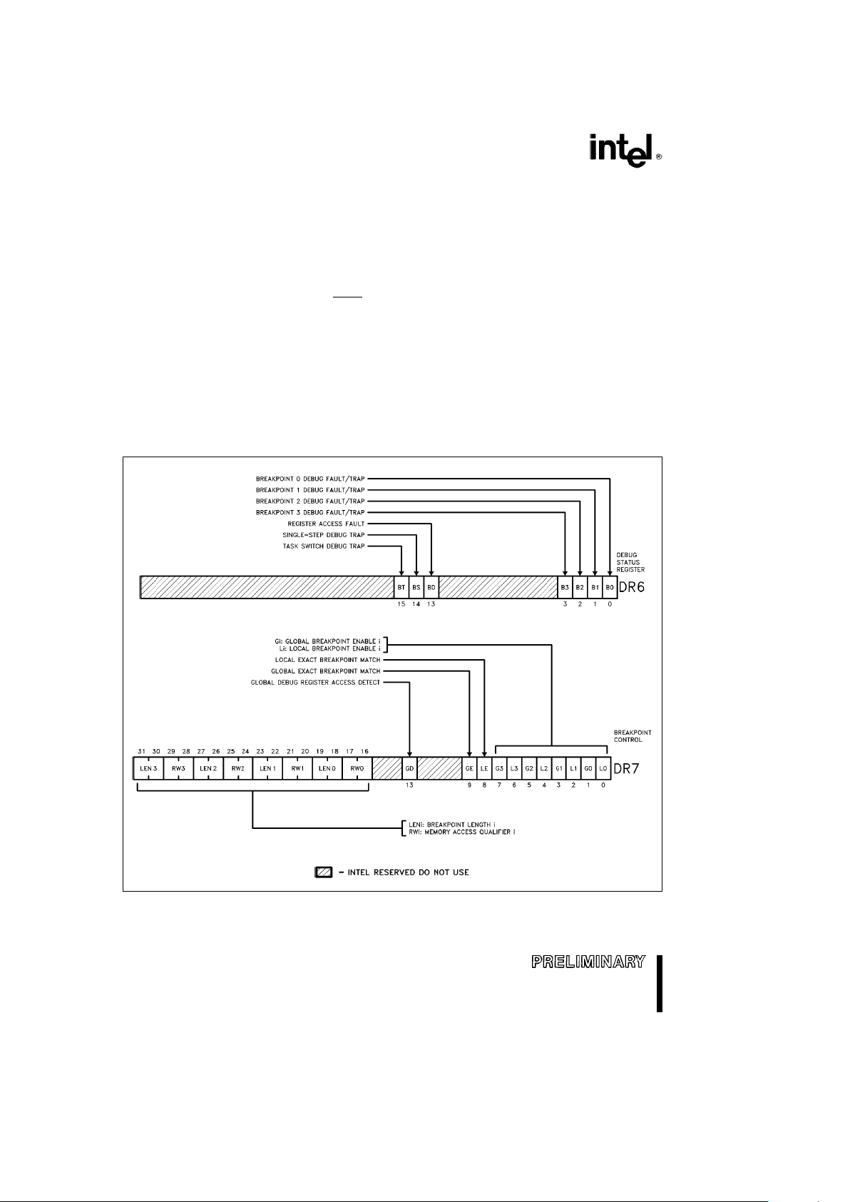
DEBUG REGISTERS
240182– 9
240182– 10
240182– 5
Figure 2.6. Debug Registers
22
376 EMBEDDED PROCESSOR
SINGLE-STEP TRAP
If the single-step flag (TF, bit 8) in the EFLAG register is found to be set at the end of an instruction, a
single-step exception occurs. The single-step exception is auto vectored to exception number 1.
The Debug Registers are an advanced debugging
feature of the 80376. They allow data access breakpoints as well as code execution breakpoints. Since
the breakpoints are indicated by on-chip registers,
an instruction execution breakpoint can be placed in
ROM code or in code shared by several tasks, neither of which can be supported by the INT 3 breakpoint opcode.
The 80376 contains six Debug Registers, consisting
of four breakpoint address registers and two breakpoint control registers. Initially after reset, breakpoints are in the disabled state; therefore, no breakpoints will occur unless the debug registers are
programmed. Breakpoints set up in the Debug
Registers are auto-vectored to exception 1.
Figure 2.6 shows the breakpoint status and control
registers.
3.0 ARCHITECTURE
The Intel 80376 Embedded Processor has a physical address space of 16 Mbytes (2
24
bytes) and allows the running of virtual memory programs of almost unlimited size (16 Kbytes
c
16 Mbytes or
256 Gbytes (2
38
bytes)). In addition the 80376 provides a sophisticated memory management and a
hardware-assisted protection mechanism.
3.1 Addressing Mechanism
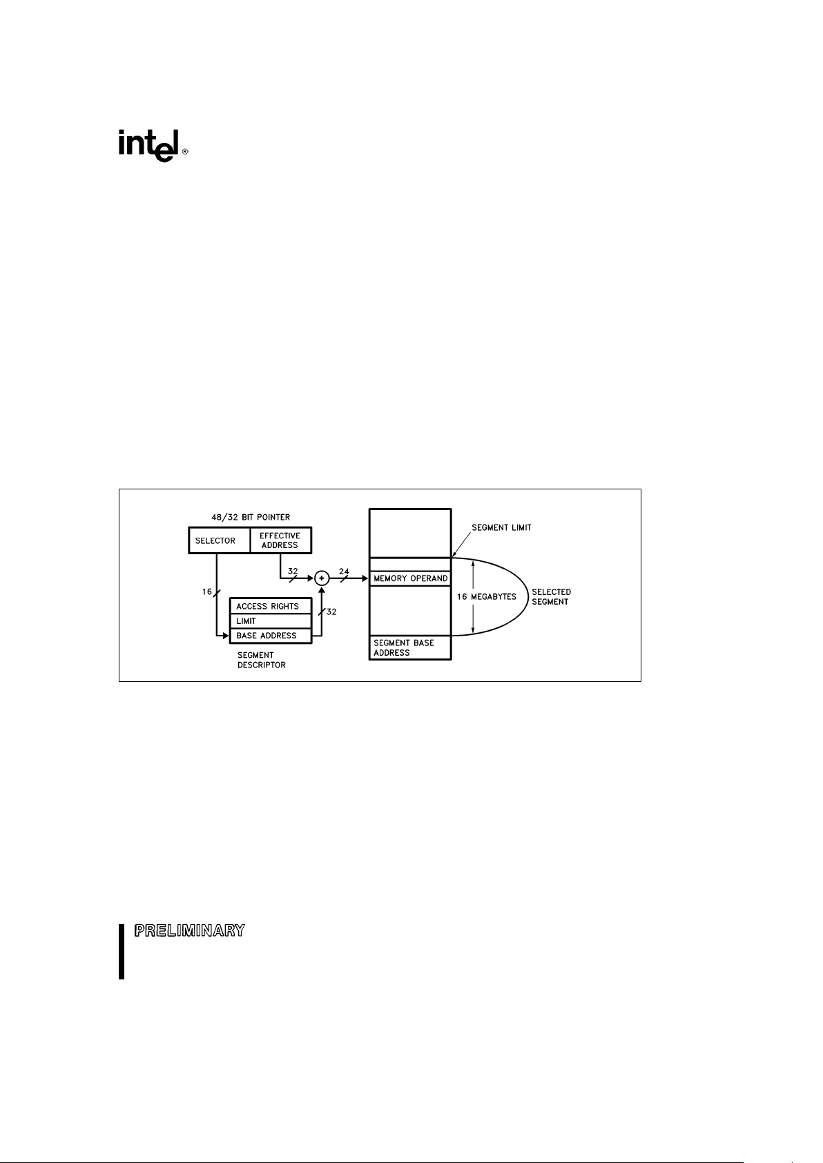
The 80376 uses two components to form the logical
address, a 16-bit selector which determines the linear base address of a segment, and a 32-bit effective address. The selector is used to specify an
index into an operating system defined table (see
Figure 3.1). The table contains the 32-bit base address of a given segment. The linear address is
formed by adding the base address obtained from
the table to the 32-bit effective address. This value
is truncated to 24 bits to form the physical address,
which is then placed on the address bus.
240182– 11
Figure 3.1. Address Calculation
23
376 EMBEDDED PROCESSOR
3.2 Segmentation
Segmentation is one method of memory management and provides the basis for protection in the
80376. Segments are used to encapsulate regions
of memory which have common attributes. For example, all of the code of a given program could be
contained in a segment, or an operating system table may reside in a segment. All information about
each segment, is stored in an 8-byte data structure
called a descriptor. All of the descriptors in a system
are contained in tables recognized by hardware.
TERMINOLOGY
The following terms are used throughout the discussion of descriptors, privilege levels and protection:
PL: Privilege LevelÐOne of the four hierarchical
privilege levels. Level 0 is the most privileged
level and level 3 is the least privileged.
RPL: Requestor Privilege LevelÐThe privilege
level of the original supplier of the selector.
RPL is determined by the least two significant
bits of a selector.
DPL: Descriptor Privilege LevelÐThis is the least
privileged level at which a task may access
that descriptor (and the segment associated
with that descriptor). Descriptor Privilege Level is determined by bits 6:5 in the Access
Right Byte of a descriptor.
CPL: Current Privilege LevelÐThe privilege level
at which a task is currently executing, which
equals the privilege level of the code segment being executed. CPL can also be determined by examining the lowest 2 bits of the
CS register, except for conforming code segments.
EPL: Effective Privilege LevelÐThe effective
privilege level is the least privileged of the
RPL and the DPL. EPL is the numerical maximum of RPL and DPL.
Task: One instance of the execution of a program.
Tasks are also referred to as processes.
DESCRIPTOR TABLES
The descriptor tables define all of the segments
which are used in an 80376 system. There are three
types of tables on the 80376 which hold descriptors:
the Global Descriptor Table, Local Descriptor Table,
and the Interrupt Decriptor Table. All of the tables
are variable length memory arrays, they can range in
size between 8 bytes and 64 Kbytes. Each table can
hold up to 8192 8-byte descriptors. The upper 13
bits of a selector are used as an index into the descriptor table. The tables have registers associated
with them which hold the 32-bit linear base address,
and the 16-bit limit of each table.
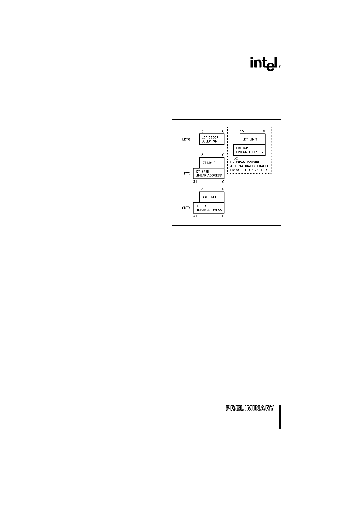
Each of the tables have a register associated with it:
GDTR, LDTR and IDTR; see Figure 3.2. The LGDT,
LLDT and LIDT instructions load the base and limit
of the Global, Local and Interrupt Descriptor Tables
into the appropriate register. The SGDT, SLDT and
SIDT store these base and limit values. These are
privileged instructions.
240182– 12
Figure 3.2. Descriptor Table Registers
Global Descriptor Table
The Global Descriptor Table (GDT) contains descriptors which are possibly available to all of the
tasks in a system. The GDT can contain any type of
segment descriptor except for interrupt and trap descriptors. Every 80376 system contains a GDT. A
simple 80376 system contains only 2 entries in the
GDT; a code and a data descriptor. For maximum
performance, descriptor tables should begin on
even addresses.
The first slot of the Global Descriptor Table corresponds to the null selector and is not used. The null
selector defines a null pointer value.
Local Descriptor Table
LDTs contain descriptors which are associated with
a given task. Generally, operating systems are designed so that each task has a separate LDT. The
LDT may contain only code, data, stack, task gate,
and call gate descriptors. LDTs provide a mechanism for isolating a given task’s code and data segments from the rest of the operating system, while
the GDT contains descriptors for segments which
are common to all tasks. A segment cannot be accessed by a task if its segment descriptor does not
exist in either the current LDT or the GDT. This pro-
24
376 EMBEDDED PROCESSOR
vides both isolation and protection for a task’s segments, while still allowing global data to be shared
among tasks.
Unlike the 6-byte GDT or IDT registers which contain
a base address and limit, the visible portion of the
LDT register contains only a 16-bit selector. This selector refers to a Local Descriptor Table descriptor in
the GDT (see Figure 2.1).
INTERRUPT DESCRIPTOR TABLE
The third table needed for 80376 systems is the Interrupt Descriptor Table. The IDT contains the descriptors which point to the location of up to 256
interrupt service routines. The IDT may contain only
task gates, interrupt gates and trap gates. The IDT
should be at least 256 bytes in size in order to hold
the descriptors for the 32 Intel Reserved Interrupts.
Every interrupt used by a system must have an entry
in the IDT. The IDT entries are referenced by INT
instructions, external interrupt vectors, and exceptions.
DESCRIPTORS
The object to which the segment selector points to
is called a descriptor. Descriptors are eight-byte
quantities which contain attributes about a given
region of linear address space. These attributes include the 32-bit logical base address of the seg-
ment, the 20-bit length and granularity of the segment, the protection level, read, write or execute
privileges, and the type of segment. All of the attribute information about a segment is contained in 12
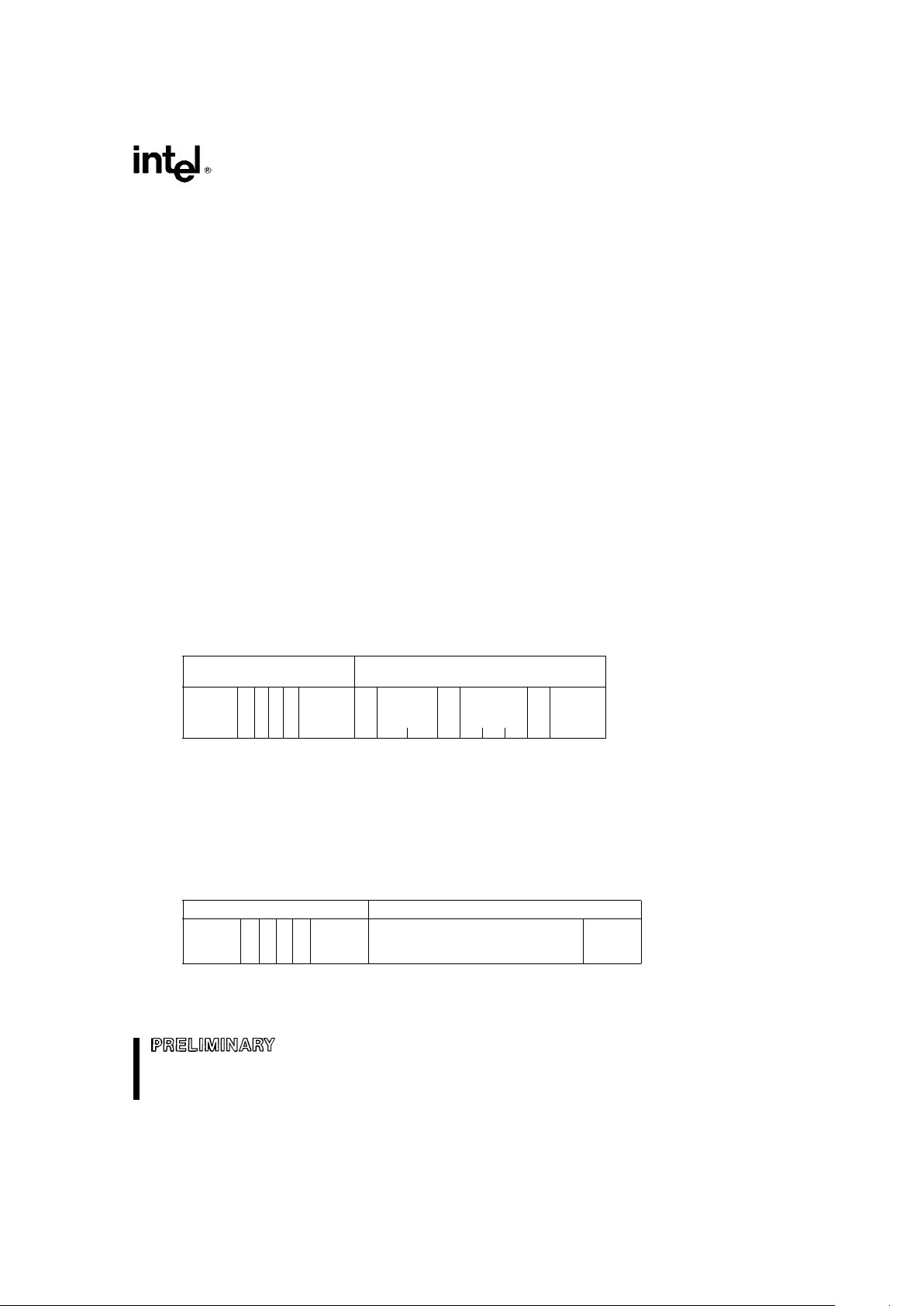
bits in the segment descriptor. Figure 3.3 shows the
general format of a descriptor. All segments on the
the 80376 have three attribute fields in common: the
Present bit (P), the Descriptor Privilege Level bits
(DPL) and the Segment bit (S). P
e
1 if the segment
is loaded in physical memory, if P
e
0 then any
attempt to access the segment causes a not present
exception (exception 11). The DPL is a two-bit field
which specifies the protection level, 0–3, associated
with a segment.
The 80376 has two main categories of segments:
system segments, and non-system segments (for
code and data). The segment bit, S, determines if a
given segment is a system segment, a code segment or a data segment. If the S bit is 1 then the
segment is either a code or data segment, if it is 0
then the segment is a system segment.
Note that although the 80376 is limited to a
16-Mbyte Physical address space (2
24
), its base address allows a segment to be placed anywhere in a
4-Gbyte linear address space. When writing code for
the 80376, users should keep code portability to an
80386 processor (or other processors with a larger
physical address space) in mind. A segment base
address can be placed anywhere in this 4-Gbyte linear address space, but a physical address will be
31 0 BYTE
ADDRESS
SEGMENT BASE 15...0 SEGMENT LIMIT 15...0 0
BASE
A
LIMIT BASE
a
4
31...24
G10V
19...16
P DPL S TYPE A
23...16
L
BASE Base Address of the segment
LIMIT The length of the segment
P Present Bit 1
e
Present 0eNot Present
DPL Descriptor Privilege Level 0 –3
S Segment Descriptor: 0
e
System Descriptor, 1eCode or Data Descriptor
TYPE Type of Segment
A Accessed Bit
G Granularity Bit 1
e
Segment length is 4 Kbyte Granular
0
e
Segment length is byte granular
0 Bit must be zero (0) for compatibility with future processors
AVL Available field for user or OS
Figure 3.3. Segment Descriptors
31 0
SEGMENT BASE 15...0 SEGMENT LIMIT 15...0 0
BASE
A
LIMIT
ACCESS
BASE
31...24
G10V
19...16
RIGHTS
23...16
a
4
L BYTE
G Granularity Bit 1eSegment length is 4 Kbyte granular
0
e
Segment length is byte granular
0 Bit must be zero (0) for compatibility with future processors
AVL Available field for user or OS
Figure 3.4. Code and Data Descriptors
25

376 EMBEDDED PROCESSOR
Table 3.1. Access Rights Byte Definition for Code and Data Descriptors
Bit
Name Function
Position
7 Present (P) Pe1 Segment is mapped into physical memory.
P
e
0 No mapping to physical memory exits
6–5 Descriptor Privilege Segment privilege attribute used in privilege tests.
Level (DPL)
4 Segment Se1 Code or Data (includes stacks) segment descriptor
Descriptor (S) S
e
0 System Segment Descriptor or Gate Descriptor
3 Executable (E) Ee0 Descriptor type is data segment: If
2 Expansion ED
e
0 Expand up segment, offsets must beslimit. Data
Direction (ED) ED
e
1 Expand down segment, offsets must bellimit. Segment
1 Writable (W) (S
e
1,We0 Data segment may not be written into.
E
e
0)*W
e
1 Data segment may be written into.
3 Executable (E) IfEe1 Descriptor type is code segment:
2 Conforming (C) CodeC
e
1 Code segment may only be executed when
SegmentCPL
t
DPL and CPL remains unchanged.
1 Readable (R) (S
e
1,Re0 Code segment may not be read.
E
e
1)*R
e
1 Code segment may be read.
0 Accessed (A) Ae0 Segment has not been accessed.
Ae1 Segment selector has been loaded into segment register
or used by selector test instructions.
generated that is a truncated version of this linear
address. Truncation will be to the maximum number
of address bits. It is recommended to place EPROM
at the highest physical address and DRAM at the
lowest physical addresses.
Code and Data Descriptors (S
e
1)
Figure 3.4 shows the general format of a code and
data descriptor and Table 3.1 illustrates how the bits
in the Access Right Byte are interpreted.
Code and data segments have several descriptor
fields in common. The accessed bit, A, is set whenever the processor accesses a descriptor. The granularity bit, G, specifies if a segment length is 1-bytegranular or 4-Kbyte-granular. Base address bits
31–24, which are normally found in 80386 descriptors, are not made externally available on the 80376.
They do not affect the operation of the 80376. The
A
31–A24
field should be set to allow an 80386 to
correctly execute with EPROM at the upper 4096
Mbytes of physical memory.
System Descriptor Formats (S
e
0)
System segments describe information about operating system tables, tasks, and gates. Figure 3.5
shows the general format of system segment descriptors, and the various types of system segments.
80376 system descriptors (which are the same as
80386 descriptor types 2, 5, 9, B, C, E and F) contain
a 32-bit logical base address and a 20-bit segment
limit.
Selector Fields
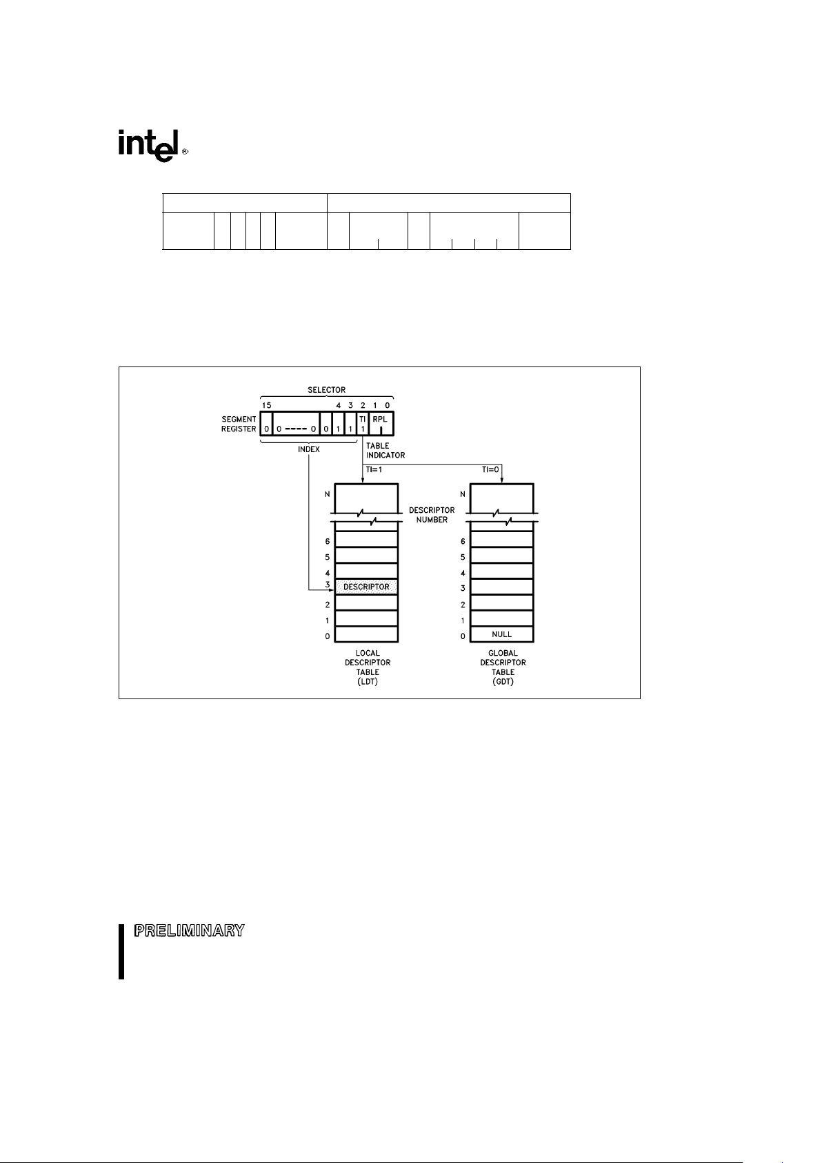
A selector has three fields: Local or Global Descriptor Table Indicator (TI), Descriptor Entry Index (Index), and Requestor ( the selector’s) Privilege Level
(RPL) as shown in Figure 3.6. The TI bit selects either the Global Descriptor Table or the Local Descriptor Table. The Index selects one of 8K descriptors in the appropriate descriptor table. The RPL bits
allow high speed testing of the selector’s privilege
attributes.
Segment Descriptor Cache
In addition to the selector value, every segment register has a segment descriptor cache register associated with it. Whenever a segment register’s contents are changed, the 8-byte descriptor associated
with that selector is automatically loaded (cached)
on the chip. Once loaded, all references to that segment use the cached descriptor information instead
of reaccessing the descriptor. The contents of the
descriptor cache are not visible to the programmer.
Since descriptor caches only change when a segment register is changed, programs which modify
the descriptor tables must reload the appropriate
segment registers after changing a descriptor’s
value.
26
376 EMBEDDED PROCESSOR
31 16 0
SEGMENT BASE 15...0 SEGMENT LIMIT 15...0 0
BASE
G000
LIMIT
P DPL 0 TYPE
BASE
a
4
31...24 19...16 23...16
Type Defines Type Defines
0 Invalid 8 Invalid
1 Reserved 9 Available 80376/80386 TSS
2 LDT A Undefined (Intel Reserved)
3 Reserved B Busy 80376/80386 TSS
4 Reserved C 80376/80386 Call Gate
5 Task Gate (80376/80386 Task) D Undefined (Intel Reserved)
6 Reserved E 80376/80386 Interrupt Gate
7 Reserved F 80376/80386 Trap Gate
Figure 3.5. System Descriptors
240182– 13
Figure 3.6. Example Descriptor Selection
3.3 Protection
The 80376 offers extensive protection features.
These protection features are particularly useful in
sophisticated embedded applications which use
multitasking real-time operating systems. For simpler embedded applications these protection capabilities can be easily bypassed by making all applications run at privilege level (PL) 0.
RULES OF PRIVILEGE
The 80376 controls access to both data and procedures between levels of a task, according to the following rules.
ÐData stored in a segment with privilege level p
can be accessed only by code executing at a
privilege level at least as privileged as p.
ÐA code segment/procedure with privilege level p
can only be called by a task executing at the
same or a lesser privilege level than p.
PRIVILEGE LEVELS
At any point in time, a task on the 80376 always
executes at one of the four privilege levels. The Current Privilege Level (CPL) specifies what the task’s
privilege level is. A task’s CPL may only be changed
27

376 EMBEDDED PROCESSOR
by control transfers through gate descriptors to a
code segment with a different privilege level. Thus,
an application program running at PL
e
3 may call an
operating system routine at PL
e
1 (via a gate) which
would cause the task’s CPL to be set to 1 until the
operating system routine was finished.
Selector Privilege (RPL)
The privilege level of a selector is specified by the
RPL field. The selector’s RPL is only used to establish a less trusted privilege level than the current
privilege level of the task for the use of a segment.
This level is called the task’s effective privilege level
(EPL). The EPL is defined as being the least privileged (numerically larger) level of a task’s CPL and a
selector’s RPL. The RPL is most commonly used to
verify that pointers passed to an operating system
procedure do not access data that is of higher privilege than the procedure that originated the pointer.
Since the originator of a selector can specify any
RPL value, the Adjust RPL (ARPL) instruction is provided to force the RPL bits to the originator’s CPL.
I/O Privilege
The I/O privilege level (IOPL) lets the operating system code executing at CPL
e
0 define the least privileged level at which I/O instructions can be used. An
exception 13 (General Protection Violation) is generated if an I/O instruction is attempted when the CPL
of the task is less privileged than the IOPL. The
IOPL is stored in bits 13 and 14 of the EFLAGS register. The following instructions cause an exception
13 if the CPL is greater than IOPL: IN, INS, OUT,
OUTS, STI, CLI and LOCK prefix.
Descriptor Access
There are basically two types of segment accessess: those involving code segments such as control transfers, and those involving data accesses.
Determining the ability of a task to access a segment involves the type of segment to be accessed,
the instruction used, the type of descriptor used and
CPL, RPL, and DPL as described above.
Any time an instruction loads a data segment register (DS, ES, FS, GS) the 80376 makes protection
validation checks. Selectors loaded in the DS, ES,
FS, GS registers must refer only to data segment or
readable code segments.
Finally the privilege validation checks are performed.
The CPL is compared to the EPL and if the EPL is
more privileged than the CPL, an exception 13 (general protection fault) is generated.
The rules regarding the stack segment are slightly
different than those involving data segments. Instructions that load selectors into SS must refer to
data segment descriptors for writeable data segments. The DPL and RPL must equal the CPL of all
other descriptor types or a privilege level violation
will cause an exception 13. A stack not present fault
causes an exception 12.
PRIVILEGE LEVEL TRANSFERS
Inter-segment control transfers occur when a selector is loaded in the CS register. For a typical system
most of these transfers are simply the result of a call
or a jump to another routine. There are five types of
control transfers which are summarized in Table 3.2.
Many of these transfers result in a privilege level
transfer. Changing privilege levels is done only by
control transfers, using gates, task switches, and interrupt or trap gates.
Control transfers can only occur if the operation
which loaded the selector references the correct descriptor type. Any violation of these descriptor usage
rules will cause an exception 13.
CALL GATES
Gates provide protected indirect CALLs. One of the
major uses of gates is to provide a secure method of
privilege transfers within a task. Since the operating
system defines all of the gates in a system, it can
ensure that all gates only allow entry into a few trusted procedures.
28

376 EMBEDDED PROCESSOR
Table 3.2. Descriptor Types Used for Control Transfer
Control Transfer Types Operation Types
Descriptor Descriptor
Referenced Table
Intersegment within the same privilege level JMP, CALL, RET, IRET* Code Segment GDT/LDT
Intersegment to the same or higher privilege level CALL Call Gate GDT/LDT
Interrupt within task may change CPL
Interrupt Instruction, Trap or IDT
Exception, External Interrupt
Interrupt Gate
Intersegment to a lower privilege level RET, IRET* Code Segment GDT/LDT
(changes task CPL)
CALL, JMP Task State GDT
Segment
Task Switch CALL, JMP Task Gate GDT/LDT
IRET** Task Gate IDT
Interrupt Instruction,
Exception, External
Interrupt
*NT (Nested Task bit of flag register)e0
**NT (Nested Task bit of flag register)
e
1
29
 Loading...