


E
DATASHEET
ADDENDUM
82371AB (PIIX4) PCI
Timing Specifications
Order Number: 290548-001
ISA IDE Xcelerator
September 1997

Information in this document is provided in connection with Intel products. No license, express or implied, by estoppel or
COPYRIGHT © INTEL CORPORATION, 1997 CG-041493
otherwise, to any intellectual property rights is granted by this document. Except as provided in Intel’s Terms and Conditions
of Sale for such products, Intel assumes no liability whatsoever, and Intel disclaims any express or implied warranty, relating
to sale and/or use of Intel products including liability or warranties relating to fitness for a particular purpose, merchantability,
or infringement of any patent, copyright or other intellectual property right. Intel products are not intended for use in medical,
life saving, or life sustaining applications.
Intel may make changes to specifications and product descriptions at any time, without notice.
The 82371AB (PIIX4) may contain design defects or errors known as errata which may cause the product to deviate from
published specifications. Current characterized errata are available on request.
*Third-party brands and names are the property of their respective owners.
Contact your local Intel sales office or your distributor to obtain the latest specifications and before placing your product order.
Copies of documents which have an ordering number and are referenced in this document, or other Intel literature, may be
obtained from:
Intel Corporation
P.O. Box 5937
Denver, CO 80217-4725
or call 1-800-548-4725

E 82371AB (PIIX4) PCI ISA IDE XCELERATOR TIMING SPECIFICATIONS
PRELIMINARY
82371AB (PIIX4) PCI ISA IDE
XCELERATOR FEATURES
Supported Kits for both Pentium and
Pentium
82430TX ISA Kit
82440LX ISA/DP Kit
Multifunction PCI to ISA Bridge
Supports PCI at 30 MHz and 33
Supports PCI Rev 2.1 Specification
Supports Full ISA or Extended I/O
Supports full Positive Decode or
Supports ISA/EIO at 1/4 of PCI
Supports Both Mobile and Desktop
Deep Green Environments
3.3V Operation With 5V Tolerant
Ultra-Low Power for Mobile
Power-On Suspend and Soft-OFF
All Registers Readable/Restorable
Power Management Logic
Global and Local Device
Suspend/Resume Logic
Supports Thermal Alarm
Support for External
Full Support for Advanced
Integrated IDE Controller
Independent Timing of Up to
PIO Mode 4 Transfers Up to
Pro Microprocessors
MHz
(EIO) Bus
Subtractive Decode of PCI
Frequency
Buffers
Environments
for Desktop Environment
for Proper Resume From 0V
Suspend
Management
Microcontroller
Configuration and Power Interface
(ACPI) Specification and OS
Directed Power Management
4 Drives
14 Mbytes/sec
Supports “Ultra DMA/33”
Synchronous DMA Mode Transfers
Up to 33 Mbytes/sec
Integrated 8 x 32-Bit Buffer for IDE
PCI Burst Transfers
Supports Glue-Less “Swap-Bay”
Option With Full Electrical Isolation
Enhanced DMA Controller
Two 82C37 DMA Controllers
Supports PCI DMA With 3 PC/PCI
Channels and Distributed DMA
Protocols (Simultaneously)
Fast Type-F DMA for Reduced PCI
Bus Usage
Interrupt Controller Based on Two
82C59
15 interrupt support
Independently Programmable for
Edge/Level Sensitivity
Supports Optional I/O APIC
Serial Interrupt Input
Timers based on 82C54
System Timer, Refresh Request,
Speaker Tone Output
USB
Two USB 1.0 Ports for Serial
Transfers at 12 or 1.5 Mbit/sec
Supports Legacy Keyboard and
Mouse Software With USB-Based
Keyboard and Mouse
Supports UHCI Design Guide
Revision 1.1 Interface
SMBus
Host interface Allows CPU to
Communicate via SMBus
Slave Interface Allows External
SMBus Master to Control Resume
Events
Real-Time Clock
256-Byte Battery-Back CMOS
SRAM
Includes Date Alarm
Two 8-Byte Lockout Ranges
1

82371AB (PIIX4) PCI ISA IDE XCELERATOR TIMING SPECIFICATIONS E
PRELIMINARY
Microsoft Windows* 95 Compliant 324 mBGA Package
REFERENCE INFORMATION: The information in this document is provided as a supplement to the standard
package datasheets published for the Intel 82371AB (PIIX4) PCI ISA IDE Xcelerator. Please refer to the
standard package datasheet (order number 290562 for the PIIX4) for product information and specifications
not found in this document.
NOTICE: This document contains information on products in the sampling and initial production phases of
development. The specifications are subject to change without notice. Verify with your local Intel Sales office
that you have the latest datasheet before finalizing a design.
The 82371AB (PIIX4) may contain design defects or errors known as errata which may cause the product to
deviate from published specifications. Current characterized errata are available on request.
2

E 82371AB (PIIX4) PCI ISA IDE XCELERATOR TIMING SPECIFICATIONS
PRELIMINARY
1.0. INTRODUCTION............................................................................................................................... 5
2.0. ELECTRICAL CHARACTERISTICS...................................................................................................5
2.1. Absolute Maximum Ratings............................................................................................................5
2.2. D.C. Characteristics ......................................................................................................................6
2.3. A.C. Characteristics .................................................................................................................... 10
2.4. Clock, Reset, ISA Bus, X-Bus and Host Timing Diagrams ............................................................. 29
2.5. PCI Timing Diagrams................................................................................................................... 48
2.6. IDE Timing Diagrams................................................................................................................... 51
2.7. USB Timing Diagrams.................................................................................................................. 53
2.8. IOAPIC Timing Diagrams............................................................................................................. 54
2.9. SMBus Timing Diagrams.............................................................................................................. 55
2.10. Ultra DMA/33 Timing Diagrams .................................................................................................. 56
FIGURES
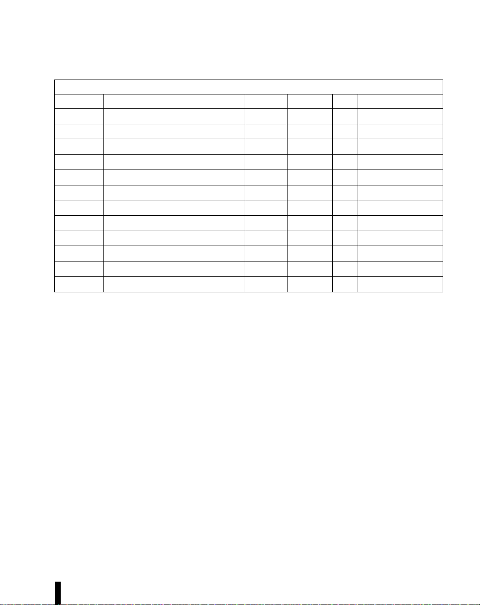
Figure 1. Test Load ............................................................................................................................ 29
Figure 2. Clock Timing........................................................................................................................ 29
Figure 3. Reset Inactive Timing........................................................................................................... 30
Figure 4. Reset Active Pulse Width..................................................................................................... 30
Figure 5. SMI#, EXTSMI# and STPCLK# Timing.................................................................................. 31
Figure 6. Input to PCICLK Setup/Hold Times ....................................................................................... 31
Figure 7. HCLKIN to Output Valid Delay .............................................................................................. 32
Figure 8. 8-Bit ISA Memory Slave Timing (PIIX4 as Master)................................................................. 32
Figure 9. 16-Bit ISA Memory Slave Timing (PIIX4 as Master)............................................................... 33
Figure 10. 8-Bit ISA I/O Slave Timing (PIIX4 as Master) ...................................................................... 34
Figure 11. 16-Bit I/O Slave Timing (PIIX4 as Master)........................................................................... 35
Figure 12. ISA Master Accessing PCI Memory Timing......................................................................... 36
Figure 13. ISA Master Accessing PIIX4 Register Timing...................................................................... 37
Figure 14. NMI Timing........................................................................................................................ 37
Figure 15. Interrupt Timing.................................................................................................................. 38
Figure 16. ISA Master Miscellaneous Timing....................................................................................... 38
Figure 17. ISA Master Data Swap Timing ............................................................................................ 39
Figure 18. DMA Compatible Timing (Memory Read)............................................................................. 40
Figure 19. DMA Compatible Timing (Memory Write)............................................................................. 41
Figure 20. DMA Compatible Timing (Data Swap).................................................................................. 42
Figure 21. DMA Type F Timing............................................................................................................ 43
Figure 22. PIIX4-Initiated Refresh Timing ............................................................................................ 44
Figure 23. ISA Master-Initiated Refresh Timing.................................................................................... 45
Figure 24. PIIX4 and ISA Master Access to X-Bus Timing.................................................................... 46
CONTENTS
PAGE
3

82371AB (PIIX4) PCI ISA IDE XCELERATOR TIMING SPECIFICATIONS E
PRELIMINARY
Figure 25. Coprocessor Error and Mouse Support Timing.....................................................................47
Figure 26. Real Time Clock Timing (RTCALE Generation)....................................................................47
Figure 27. Speaker Timing ..................................................................................................................48
Figure 28. Propagation Delay ..............................................................................................................48
Figure 29. Valid Delay From Rising Clock Edge ...................................................................................49
Figure 30. Setup and Hold Times.........................................................................................................49
Figure 31. Float Delay.........................................................................................................................50
Figure 32. Pulse Width........................................................................................................................50
Figure 33. Output Enable Delay...........................................................................................................50
Figure 34. IDE PIO Mode....................................................................................................................51
Figure 35. IDE Multiword DMA Mode...................................................................................................52
Figure 36. Data Signal Rise and Fall Time............................................................................................53
Figure 37. Data Jitter..........................................................................................................................53
Figure 38. EOP Width Timing..............................................................................................................54
Figure 39. PIIX4 to IOAPIC Timing ......................................................................................................54
Figure 40. SMBus Timing....................................................................................................................55
Figure 41. SMBus Timeout Timing.......................................................................................................55
Figure 42. Ultra DMA/33 Drive Initiating a DMA Burst for a Read Command..........................................56
Figure 43. Ultra DMA/33 Sustained Synchronous DMA Burst................................................................57
Figure 44. Ultra DMA/33 Sustained Synchronous DMA Burst................................................................58
Figure 45. Ultra DMA/33 Host Terminating a DMA Burst During a Write Command................................58
TABLES
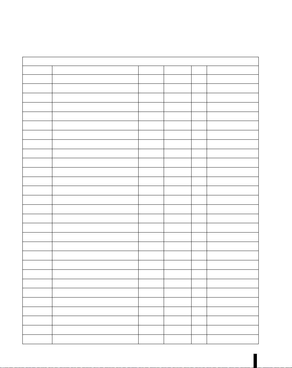
Table 1. Package Thermal Resistance...................................................................................................5
Table 2. DC Characteristics ..................................................................................................................6
Table 3. DC Characteristic Signal Association .......................................................................................8
Table 4. DC Current Characteristics......................................................................................................9
Table 5. Clock/Reset Timings..............................................................................................................10
Table 6. ISA Bus and X-Bus Timings ...................................................................................................12
Table 7. PCI Interface Timing..............................................................................................................23
Table 8. PCI Bus IDE Timing...............................................................................................................24
Table 9. Universal Serial Bus Timing...................................................................................................26
Table 10. IOAPIC Bus Timing..............................................................................................................27
Table 11. SMBUS Timing....................................................................................................................27
Table 12. Serial IRQ Timing ................................................................................................................28
Table 13. Ultra DMA/33 Timing............................................................................................................28
Table 14. A.C. Test Loads...................................................................................................................29
4

E 82371AB (PIIX4) PCI ISA IDE XCELERATOR TIMING SPECIFICATIONS
PRELIMINARY
1.0. INTRODUCTION
This document contains the Electrical and the Thermal Specification (ETS) for the 82371AB (PIIX4). PIIX4 is
a multi-function PCI device implementing a PCI-to-ISA bridge function, a PCI IDE function, a Universal Serial
Bus Host/Hub function, and a Power Management function.
The contents of this document are based on simulation and parametric data. This information may be
modified as more data is available.
REFERENCES
The ETS assumes that the reader is familiar with the following documents:
• 82371AB PIIX4 External Design Specification
• Universal Serial Bus Specification
• Universal Host Controller Interface (UHCI) Design Guide
• System Management Bus Specification
• Serialized IRQ Support for PCI Systems Specification
• Distributed DMA Support for PCI Systems Specification
2.0. ELECTRICAL CHARACTERISTICS
2.1. Absolute Maximum Ratings
Case Temperature under Bias ............................................0oC to +85oC
Storage Temperature .........................................................-55oC to +150oC
Voltage on Any Pin with Respect to Ground ........................-0.3 to V
3.3V Supply Voltage with Respect to Vss............................-0.3 to +4.6V
5.0V Supply Voltage with Respect to Vss (V
Maximum Power Dissipation ..............................................1.0W
WARNING: Stressing the device beyond the “Absolute Maximum Ratings” may cause permanent
The 82371AB PIIX4 (BGA) is designed for operation at case temperatures between 0oC and 85oC. The
thermal resistances of the package are given in Table 1.
Thetaja (oC/Watt) 29 24.5
Thetajc (oC/Watt) 9.0
CC + 0.3V
REF).................-0.3 to +5.5V
damage. These are stress ratings only. Operating beyond the “Operating Conditions” is not
recommended and extended exposure beyond “Operating Conditions” may affect reliability.
Table 1. Package Thermal Resistance
Parameter Air Flow
Meters/Second (Linear Feet per Minute)
0 (0) 1.0 (196.9)
5
82371AB (PIIX4) PCI ISA IDE XCELERATOR TIMING SPECIFICATIONS E
PRELIMINARY
2.2. D.C. Characteristics
Table 2. DC Characteristics
Functional Operating Range (V
Symbol Parameter Min Max Unit Notes
VCC(RTC) Battery Voltage 2.0 3.6 V
VCC(SUS) Standby Voltage 3.0 3.6 V
VIL1 Input Low Voltage -0.5 0.3 VCC V 1
VIH1 Input High Voltage 0.5 VCC VCC + 0.5 V 1
VIL2 Input Low Voltage -0.3 0.6 V 1
VIH2 Input High Voltage 1.4 VCC + 0.3 V 1
VIL3 Input Low Voltage -0.5 0.8 V 1
VIH3 Input High Voltage 2.0 VCC5 + 0.5 V 1
VOL1 Output Low Voltage 0.4 V 1
VOH1 Output High Voltage VCC - 0.5 V 1
VOL2 Output Low Voltage 0.3 V 1, 2
VOH2 Output High Voltage 2.8 3.6 V 1, 2
VOL3 Output Low Voltage 0.5 V 1
VOH3 Output High Voltage VCC - 0.5 V 1
VOL4 Output Low Voltage 0.45 V 1
VOH4 Output High Voltage VCC - 0.5 V 1
VDI Differential Input Sensitivity 0.2 V |(USBPx+, USBPx-)|
VCM Differential Common Mode Range 0.8 2.5 V Includes VDI
VSE Single Ended Rcvr Threshold 0.8 2.0 V
IOL1 Output Low Current 4 mA 1, @ VOL1
IOH1 Output High Current -1 mA 1, @ VOH1
IOL2 Output Low Current 10 mA 1, @ VOL4
IOH2 Output High Current -3 mA 1, @ VOH4
IOL3 Output Low Current 3 mA 1, @ VOL1
IOH3 Output High Current -2 mA 1, @ VOH1
IOL4 Output Low Current 6 mA 1, @ VOL1
IOH4 Output High Current -2 mA 1, @ VOH1
IOL5 Output Low Current 2 mA 1, @ VOL2
IOH5 Output High Current -0.25 mA 1, @ VOH2
REF=5V ±±5%, VCC=3.3V ±±0.3V, TCASE=0°C to +85°C)
6
E 82371AB (PIIX4) PCI ISA IDE XCELERATOR TIMING SPECIFICATIONS
PRELIMINARY
Table 2. DC Characteristics
Functional Operating Range (V
Symbol Parameter Min Max Unit Notes
IOL6 Output Low Current 6 mA 1, @ VOL1
IOH6 Output High Current -2 mA 1, @ VOH1
IOL7 Output Low Current 7 mA 1, @ VOL1
IOH7 Output High Current -2 mA 1, @ VOH1
IOL8 Output Low Current 11 mA 1, @ VOL3
IOH8 Output High Current -2 mA 1, @ VOH3
ILI1 Input Leakage Current ±1 µA
ILI2 Hi-Z State Data Line Leakage -10 +10 µA (0V< VIN< 3.3V)
CIN Input Capacitance 12 pF FC=1 MHz
COUT Output Capacitance 12 pF FC=1 MHz
CI/O I/O Capacitance 12 pF FC=1 MHz
CL Crystal Load Capacitance 7.5 15 pF
NOTES:
1. Refer to Table 3. for the signals associated with this specification.
OL2 assumes RL of 1.5 kohms to 3.6V and VOH2 assumes RL of 15 kohms to GND.
2. V
REF=5V ±±5%, VCC=3.3V ±±0.3V, TCASE=0°C to +85°C)
7
82371AB (PIIX4) PCI ISA IDE XCELERATOR TIMING SPECIFICATIONS E
PRELIMINARY
Table 3. DC Characteristic Signal Association
Symbol Associated Signals
VIL1/VIH1 VREF=5.0V: (all 3.3V only inputs except SMBCLK & SMBDATA)
PWROK, RSMRST#, RTCX1, TEST, BATLOW#, CONFIG[1:2], EXTSMI#, GPI[1], IRQ8#,
LID, RI#, SMBALERT#, PWRBTN#, USBP[1:0]+, USBP[1:0]-, FERR#
REF=3.3V: (all inputs except SMBCLK & SMBDATA)
V
PWROK, RSMRST#, RTCX1, TEST, BATLOW#, CONFIG[1:2], EXTSMI#, GPI[1], IRQ8#,
LID, RI#, SMBALERT#, PWRBTN#, USBP[1:0]+, USBP[1:0]-, FERR#, AD[31:0],
C/BE[3:0]#, CLKRUN#, DEVSEL#, FRAME#, IDSEL, IRDY#, PHLDA#, SERR#, STOP#,
TRDY#, IOCHK#, IOCHRDY, IOCS16#, IOR#, IOW#, LA[23:17], MEMCS16#, MEMR#,
MEMW#, REFRESH#, SA[19:0], SBHE#, SD[15:0], ZEROWS#, A20GATE, RCIN#,
DREQ[0:3, 5:7], REQ[A:C]#, APICREQ#, IRQ[1, 3:7, 9:12, 14:15], PIRQ[A:D], SERIRQ,
CLK48, PCICLK, OSC, PDD[15:0], PDDREQ, PIORDY, SDD[15:0], SDDREQ, SIORDY,
OC[1:0]#, PCIREQ[A:D],THRM#
VIL2/VIH2 SMBCLK, SMBDATA
VIL3/VIH3 VREF=5.0V: (all 5V tolerant inputs)
AD[31:0], C/BE[3:0]#, CLKRUN#, DEVSEL#, FRAME#, IDSEL, IRDY#, PHLDA#, SERR#,
STOP#, TRDY#, IOCHK#, IOCHRDY, IOCS16#, IOR#, IOW#, LA[23:17], MEMCS16#,
MEMR#, MEMW#, REFRESH#, SA[19:0], SBHE#, SD[15:0], ZEROWS#, A20GATE,
RCIN#, DREQ[0:3, 5:7], REQ[A:C]#, APICREQ#, IRQ[1, 3:7, 9:12, 14:15], PIRQ[A:D],
SERIRQ, CLK48, PCICLK, OSC, PDD[15:0], PDDREQ, PIORDY, SDD[15:0], SDDREQ,
SIORDY, OC[1:0]#, PCIREQ[A:D],THRM#
VOL1/VOH1 PDA[2:0], PDCS1#, PDCS3#, PDD[15:0], PDDACK#, PDIOR#, PDIOW#, SDA[2:0],
VOL2/VOH2 USBP[1:0]+, USBP[1:0]-
VOL3/VOH3 SLP#
VOL4/VOH4 ISA/EIO Output Signals: AEN, BALE, IOCHRDY, IOR#, IOW#, LA[23:17], MEMCS16#,
IOL1/IOH1 IDE Output Signals: PDA[2:0], PDCS1#, PDCS3#, PDD[15:0], PDDACK#, PDIOR#,
IOL2/IOH2 ISA/EIO Output Signals: AEN, BALE, IOCHRDY, IOR#, IOW#, LA[23:17], MEMCS16#,
SDCS1#, SDCS3#, SDD[15:0], SDDACK#, SDIOR#, SDIOW#, CPU_STP#, EXTSMI#, ZZ,
GPO8, PCI_STP#, SMBCLK, SMBDATA, SUS[A:C]#, SUS_STAT[1:2]#, A20M#, CPURST,
IGNNE#, INIT, INTR, NMI, SMI#, STPCLK#, BIOSCS#, KBCCS#, MCCS#, PCS0#, PCS1#,
RTCALE, RTCCS#, XDIR#, XOE#, SUSCLK, RTCX2, SMBCLK, SMBDATA, APICACK#,
APICCS#, IRQ[0, 8], SPKR, GNT[A:C], GPO[0, 8, 27, 28, 30], IRQ9OUT#, AD[31:0],
C/BE[3:0]#, CLKRUN#, DEVSEL#, FRAME#, IRDY#, PAR, PCIRST#, PHOLD#, SERR#,
STOP#, TRDY#, SERIRQ
MEMR#, MEMW#, REFRESH#, RSTDRV, SA[19:0], SBHE#, SD[15:0], SMEMR#,
SMEMW#, SYSCLK, DACK[0:3, 5:7]#, TC
PDIOW#, SDA[2:0], SDCS1#, SDCS3#, SDD[15:0], SDDACK#, SDIOR#, SDIOW#
MEMR#, MEMW#, REFRESH#, RSTDRV, SA[19:0], SBHE#, SD[15:0], SMEMR#,
SMEMW#, SYSCLK, DACK[0:3, 5:7]#, TC
8
E 82371AB (PIIX4) PCI ISA IDE XCELERATOR TIMING SPECIFICATIONS
PRELIMINARY
Table 3. DC Characteristic Signal Association
Symbol Associated Signals
IOL3/IOH3 Power Management Signals: CPU_STP#, EXTSMI#, ZZ, GPO8, PCI_STP#, SMBCLK,
IOL4/IOH4 PCI Bus Signals: AD[31:0], C/BE[3:0]#, CLKRUN#, DEVSEL#, FRAME#, IRDY#, PAR,
IOL5/IOH5 USB Signals: USBP[1:0]+, USBP[1:0]-
IOL6/IOH6 SMI#, STPCLK#
IOL7/IOH7 INIT#
IOL8/IOH8 SLP#
Symbol Parameter Typ Max Unit Notes
ICC(3V) VCC Supply Current 110 155 mA
ICC(SUS)ONSuspend Well Supply Current—Full On 3 5 mA
SMBDATA, SUS[A:C]#, SUS_STAT[1:2]#
CPU Interface Signals: A20M#, CPURST, IGNNE#, INTR, NMI
X-Bus Interface Signals: BIOSCS#, KBCCS#, MCCS#, PCS0#, PCS1#, RTCALE,
RTCCS#, XDIR#, XOE#, SUSCLK, RTCX2
Other Signals: SMBCLK, SMBDATA, APICACK#, APICCS#, IRQ[0, 8], SPKR, GNT[A:C],
GPO[0, 8, 27, 28, 30], IRQ9OUT#
PCIRST#, PHOLD#, SERR#, STOP#, TRDY#, SERIRQ
Table 4. DC Current Characteristics
Functional Operating Range (V
REF=5V ±±5%, VCC=3.3V ±±0.3V, TCASE=0°C to +85°C)
ICC(SUS)
POS/STR
ICC(SUS)
STD/Soff
Icc(RTC) Battery Standby Current 6 8 µA VCC(RTC)=3.0V
Suspend Well Supply Current—Power On
Suspend or Suspend to RAM
Suspend Well Supply Current—Suspend to
Disk or Soft Off
30 150 µA
9 150 µA
Mech Off State
9
82371AB (PIIX4) PCI ISA IDE XCELERATOR TIMING SPECIFICATIONS E
PRELIMINARY
2.3. A.C. Characteristics
Table 5. Clock/Reset Timings
Functional Operating Range (V
Sym Parameter Min Max Units Notes Figure
PCI Clock Timings
PCICLK
t1a Period 30 33.3 ns 2
t1b High Time 12.0 ns 2
t1c Low Time 12.0 ns 2
t1c Rise Time 3.0 ns 2
t1d Fall Time 3.0 ns 2
ISA Clock Timings
SYSCLK
t1f Period 120 133.3 ns 2
t1g High Time 49 ns 2
t1h Low Time 49 ns 2
t1i Rise Time 4 ns 2
t1j Fall Time 4 ns 2
Oscillator Clock Timings
OSC
t1l OSC Period 67 70 ns 2
t1m High Time 20 2
t1n Low Time 20 ns 2
USB Clock Timings
f
clk48
t1p Frequency Tolerance ±2500 ppm 1 2
t1q High Time 7 ns 2
t1r Low Time 7 ns 2
t1s Rise Time 1.2 ns 2
t1t Fall Time 1.2 ns 2
f
susclk
t1v High Time 10 µs
t1w Low Time 10 µs
Operating Frequency 48 MHz
Suspend Clock Timings
SUSCLK Operating Frequency 32 KHz
REF=5V ±±5%, VCC=3.3V ±±0.3V, TCASE=0°C to +85°C)
10
E 82371AB (PIIX4) PCI ISA IDE XCELERATOR TIMING SPECIFICATIONS
PRELIMINARY
Table 5. Clock/Reset Timings
Functional Operating Range (V
Sym Parameter Min Max Units Notes Figure
SMBus Clock
f
smb
t2b High Time 4.0 50 µs 40
t2c Low Time 4.7 µs 40
t2d Clock/Data Rise Time 1000 ns 40
t2e Clock/Data Fall Time 300 ns 40
t2f PCIRST#, RSTDRV Driven Inactive After
t2g CPURST, PCIRST#, RSTDRV Active Pulse
t2h CPURST Driven Inactive After PCIRST# is
t2i CPURST Valid Delay from PCICLK Rising 2 25 ns 29
t2j PWROK, RSMRST# Rise Time 10 ns 3
t3a Valid Delay from PCICLK 2 25 ns 7
t3b Active Pulse Width 3 PCICLK 5
t3c Inactive Pulse Width 4 PCICLK 5
t3d Active Pulse Width 2 PCICLK 5
t3e Inactive Pulse Width 4 PCICLK 5
t3f Valid Setup to PCICLK 10 ns 6
t3g Valid Hold from PCICLK 4 ns 6
t3h Valid Delay from PCICLK 2 25 ns 7
t3i STPCLK# Inactive Pulse Width 5 PCICLK 5
NOTES:
1. The USBCLK is a 48 MHz that expects a 40/60% duty cycle.
2. The maximum high time (t2b Max) provide a simple guaranteed method for devices to detect bus idle
3. t2j is measured as a transition time through the threshold region Vol=0.8V and Voh=2.0V.
SMCLK Operating Frequency 10 16 KHz
RESET TIMINGS
SUS_STATx# is Driven Inactive.
Width. Initiated via the RC Register.
Driven Inactive.
SMI#
EXTSMI#
STPCLK#
conditions.
REF=5V ±±5%, VCC=3.3V ±±0.3V, TCASE=0°C to +85°C)
1 RTCCLK 3
1 ms 4
1 RTCCLK 3
11
82371AB (PIIX4) PCI ISA IDE XCELERATOR TIMING SPECIFICATIONS E
PRELIMINARY
Table 6. ISA Bus and X-Bus Timings
Functional Operating Range (V
Sym Parameter Min Max Units Type Size Notes Figure
PIIX4 AS MASTER TIMINGS
BALE
t4a BALE Pulse Width 50 ns M,I/O 8,16 8,9,10,
t4b BALE Driven Active from MEMx#, Iox#
Inactive
LA[23:17]
t5a LA[23:17] Valid Setup to BALE Inactive 150 ns M 8,16 7 8,9
t5b LA[23:17] Valid Hold from BALE
Inactive
t5c LA[23:17] Valid Setup to MEMx# Active 150 ns M 16 9
t5d LA[23:17] Valid Setup to MEMx# Active 173 ns M 8 8
t5e LA[23:17] Invalid from MEMx# Active 39 ns M 16 9
t5f LA[23:17] Invalid from MEMx# Active 39 ns M 8 8
SA[19:0], SBHE#
t6a SA[19:0], SBHE# Valid Setup to
MEMx# Active
t6b SA[19:0], SBHE# Valid Setup to Iox#
Active
t6c SA[19:0], SBHE# Setup to MEMx#,
Iox# Active
t6d SA[19:0], SBHE# Valid Setup to BALE
Inactive
t6e SA[19:0], SBHE# Valid Hold from
MEMx#, Iox# Inactive
MEMR#, MEMW#, IOR# AND IOW#
t7a MEMx# Active Pulse Width (std) 225 ns M 16 9
t7b Iox# Active Pulse Width (std) 160 ns I/O 16 11
t7c MEMx# Active Pulse Width (nws) 105 ns M 16 1 9
t7d MEMx# or Iox# Active Pulse Width
(std)
t7e MEMx# or Iox# Active Pulse Width
(nws)
t7f MEMx# Inactive Pulse Width 103 ns M 16 9
REF=5V ±±5%, VCC=3.3V ±±0.3V, TCASE=0°C to +85°C)
11
44 ns M,I/O 8,16 8,9,10,
11
26 ns M 8,16 8,9
34 ns M 16 13,15 9
100 ns I/O 16 11
100 ns M,I/O 8 9
37 ns M,I/O 8,16 13,15 8,9,10,
11
41 ns M,I/O 8,16 8,9,10,
11
520 ns M,I/O 8 8,10
160 ns M,I/O 8 1 8,10
12
E 82371AB (PIIX4) PCI ISA IDE XCELERATOR TIMING SPECIFICATIONS
PRELIMINARY
Table 6. ISA Bus and X-Bus Timings
Functional Operating Range (V
Sym Parameter Min Max Units Type Size Notes Figure
t7g MEMx# Inactive Pulse Width 163 ns M 8 8
t7h Iox# Inactive Pulse Width 163 ns I/O 8,16 10,11
t7i MEMx#, Iox# Driven Inactive from
IOCHRDY Active
SMEMR# and SMEMW#
t8a SMEMR# & SMEMW# Propagation
Delay from MEMR# and MEMW#
Read Data
t9a Read Data Driven from MEMR#, IOR#
Active
t9b Read Data Valid Setup to MEMR#,
IOR#
t9c Read Data Valid Hold from MEMR#,
IOR# Inactive
t9d Read Data Tri-Stated from MEMR# and
IOR# Inactive
Write Data
t10a Write Data Valid Setup to MEMW#
Active
Write Data Valid Setup to IOW# Active
Write Data Valid Setup to IOW# Active
t10b Write Data Valid Hold from MEMW#,
IOW# Inactive
t10c Write Data Tri-Stated from MEMW#,
IOW# Inactive
t10d Write Data Driven Valid after Read
MEMR#, IOR# Inactive
MEMCS16#
t11a MEMCS16# Driven Active from
LA[23:17] Valid
t11b MEMCS16# Inactive from LA[23:17]
Valid
t11c MEMCS16# Valid Hold from LA[23:17]
Invalid
REF=5V ±±5%, VCC=3.3V ±±0.3V, TCASE=0°C to +85°C)
120 ns M,I/O 8,16 8,9,10,
16 ns M 8,16 8,9
0 ns M,I/O 8,16 8,9,10,
24 ns M,I/O 8,16 8,9,10,
0 ns M,I/O 8,16 8,9,10,
41 ns M,I/O 8,16 8,9,10,
-40
-40
+23
45 ns M,I/O 8,16 8,9,10,
105 ns M,I/O 8,16 8,9,10,
41 ns M,I/O 8,16 8,9,10,
94 ns M 16 9
91 ns M 8 8
0 ns M 16 9
ns
ns
ns
M,I/O
M,I/O
M,I/O
8,16
8
16
11
11
11
11
11
8,9,10,
11
11
11
11
13
82371AB (PIIX4) PCI ISA IDE XCELERATOR TIMING SPECIFICATIONS E
PRELIMINARY
Table 6. ISA Bus and X-Bus Timings
Functional Operating Range (V
Sym Parameter Min Max Units Type Size Notes Figure
t11d MEMCS16# Driven Active from
SA[19:2] Valid
IOCS16#
t12a IOCS16# Driven Active from Valid
SA[19:0]
t12b IOCS16# Inactive from Valid SA[19:0] 91 ns I/O 8 10
t12c IOCS16# Valid Hold from SA[19:0]
Invalid
t12d IOCS16# Driven Active from Iox Active 80 ns I/O 16 11
ZEROWS#
t13a ZEROWS# Driven Active from MEMx#
Active
t13b ZEROWS# Driven Active from MEMx#,
Iox# Active
t13c ZEROWS# Driven Active from
LA[23:17] Valid
t13d ZEROWS# Driven Active from
LA[23:17] Valid
ZEROWS#
t13e ZEROWS# Driven Active from
SA[19:0], SBHE# Valid
t13f ZEROWS# Driven Active from
SA[19:0], SBHE# Valid
AEN
t14a AEN Valid Setup to Iox# Driven Active 111 ns I/O 8,16 10,11
t14b AEN Valid Setup to BALE Driven
Inactive
t14c AEN Valid Hold from Iox# Driven
Inactive
IOCHRDY
t15a IOCHRDY Driven Valid from MEMx#,
Iox# Active
t15b IOCHRDY Driven Valid from MEMx#,
Iox# Active
REF=5V ±±5%, VCC=3.3V ±±0.3V, TCASE=0°C to +85°C)
35 ns M 16 9
123 ns I/O 16 11
0 ns I/O 16 11
16 ns M 16 9
80 ns M,I/O 8 8
180 ns M 16 9
300 ns M 8 8
80 ns M 16 9
200 ns M,I/O 8 8,10
111 ns I/O 8,16 10,11
41 ns I/O 8,16 10,11
78 ns M,I/O 16 9,11
366 ns M,I/O 8 8,10
14
E 82371AB (PIIX4) PCI ISA IDE XCELERATOR TIMING SPECIFICATIONS
PRELIMINARY
Table 6. ISA Bus and X-Bus Timings
Functional Operating Range (V
Sym Parameter Min Max Units Type Size Notes Figure
t15e IOCHRDY Inactive Pulse Width 0.12 15.6 µs M,I/O 8,16 8,9,10,
PIIX4 AS SLAVE TIMINGS
LA[23:17]
t16a LA[23:17] Valid Setup to MEMx# Active 23 ns M 16 12
SA[19:0],SBHE#
t17a SA[19:0],SBHE# Setup to MEMx#
Active
t17b SA[19:0],SBHE# Setup to Iox# Active 89 ns I/O 8 13
t17c SA[19:0],SBHE# Valid Hold from
MEMx#, Iox# Inactive
MEMR#, MEMW#, IOR#, IOW#
t18a MEMx# Active Pulse Width 214 ns M 16 12
t18b Iox# Active Pulse Width 509 ns I/O 8 13
t18c MEMx# Inactive Pulse Width 92 ns M 16 12
t18d Iox# Inactive Pulse Width 152 ns I/O 8 13
Read Data
t19a Read Data Valid from IOCHRDY
Active
t19b Read Data Valid from IOR# Active 69 ns I/O 8 11 13
t19c Read Data Valid Hold from MEMR#,
IOR# Inactive
t19d Read Data Tri-State from MEMR#,
IOR# Inactive
Write Data
t20a Write Data Valid Setup to MEMW#,
IOW# Active
t20b Write Data Valid Hold from MEMW#,
IOW# Inactive
MEMCS16#
t21a MEMCS16# Driven Active from Valid
LA[23:17]
t21b MEMCS16# Float from Valid LA[23:17] 31 ns M 16 12
REF=5V ±±5%, VCC=3.3V ±±0.3V, TCASE=0°C to +85°C)
11
23 ns M 16 12
30 ns M,I/O 8,16 12,13
69 ns M,I/O 8,16 12,13
0 ns M,I/O 8,16 12,13
55 ns M,I/O 8,16 12,13
-54 ns M,I/O 8,16 12,13
14 ns M,I/O 8,16 12,13
65 ns M 16 12
15
82371AB (PIIX4) PCI ISA IDE XCELERATOR TIMING SPECIFICATIONS E
PRELIMINARY
Table 6. ISA Bus and X-Bus Timings
Functional Operating Range (V
Sym Parameter Min Max Units Type Size Notes Figure
t21c MEMCS16# Valid Hold from LA[23:17]
Invalid
IOCHRDY
t22a IOCHRDY Inactive from MEMx#, Iox#
Active
t22b IOCHRDY Float from IOCHRDY
Rising
t22c IOCHRDY Inactive Pulse Width 0.12 2.5 µs M,I/O 8,16 12,13
INTERRUPT AND NMI TIMINGS
NMI Timing
t23a SERR#, IOCHK# Active to NMI Driven
Active
Interrupt Timing
t24a IRQx Inactive Pulse Width 100 ns 15
ISA BUS MASTER TIMINGS
DACK#
t26a DACK#, Inactive from DREQ Inactive 240 ns 16
Tri-Stating and Driving the Bus
t27a PIIX4 Tri-States Address, Data, and
Control Signals from DACK#, Active
t27b PIIX4 Drives Address, Data, and
Control Signals from DACK#, Inactive
SMEMR# and SMEMW#
t28a SMEMR# and SMEMW# Active (falling
edge) from MEMR# and MEMW#
Active (falling edge)
t28b SMEMR# and SMEMW# Inactive
(rising edge) from MEMR# and
MEMW# Inactive (rising edge)
DATA SWAP LOGIC TIMING
(ISA MASTER TO ISA SLAVE)
t29a SD[7:0] to SD[15:8] Propagation Delay 26 ns 17
t29b SD[15:8] to SD[7:0] Propagation Delay 26 ns 17
REF=5V ±±5%, VCC=3.3V ±±0.3V, TCASE=0°C to +85°C)
0 ns M 16 12
50 ns M,I/O 8,16 12,13
85 ns M,I/O 8,16 4 12,13
200 ns 14
30 ns 16
71 ns 16
25 ns 16
35 ns 16
16
E 82371AB (PIIX4) PCI ISA IDE XCELERATOR TIMING SPECIFICATIONS
PRELIMINARY
Table 6. ISA Bus and X-Bus Timings
Functional Operating Range (V
Sym Parameter Min Max Units Type Size Notes Figure
t29c PIIX4 Drives Data Bus from IOR#,
IOW#, MEMR# or MEMW# Active
t29d PIIX4 Tri-States Bus from IOR#,
MEMR#, or SMEMR# Inactive
t29e PIIX4 Tri-States Bus from IOW#,
MEMW#, or SMEMW# Inactive
DMA COMPATIBLE TIMINGS
DREQ
t30a DREQ Active Hold from IOR# Active 558 ns 5 19
t30b DREQ Active Hold from IOW# Active 315 ns 5 18
DACK#
t31a DACK# Active to IOR# Active 73 ns 19
t31b DACK# Active to IOW# Active 312 ns 18
t31c DACK# Active Hold from IOR# Inactive 100 ns 19
t31d DACK# Active Hold from IOW# Inactive 155 ns 18
AEN and BALE
t32a AEN Active to Iox# Active 111 ns 18,19
t32b AEN and BALE Inactive from Iox#
Inactive
LA[23:19], SA[19:0], SBHE#
t33a LA[23:19],SA[19:0], SBHE# Valid Setup
to MEMx# Active
t33b LA[23:19],SA[19:0], SBHE# Valid Hold
from MEMx# Inactive
MEMR#, MEMW#, IOR#, IOW#
t34a IOW# and MEMW# Active Pulse Width 465 ns 18,19
t34b MEMR# Active Pulse Width 495 ns 18
t34c IOR# Active Pulse Width 760 ns 19
t34d IOW# Inactive Pulse Width
(continuous)
t34e IOR# Inactive Pulse Width (continuous) 160 ns 19
t34f IOR# Active to MEMW# Active 230 ns 19
t34g MEMR# Active to IOW# Active -26 ns 18
REF=5V ±±5%, VCC=3.3V ±±0.3V, TCASE=0°C to +85°C)
26 ns 2 17
2 55 ns 2,3 17
2 60 ns 2,3 17
41 ns 18,19
99 ns 18,19
51 ns 18,19
465 ns 18
17

82371AB (PIIX4) PCI ISA IDE XCELERATOR TIMING SPECIFICATIONS E
PRELIMINARY
Table 6. ISA Bus and X-Bus Timings
Functional Operating Range (V
Sym Parameter Min Max Units Type Size Notes Figure
t34h MEMR# Active Hold from IOW#
Inactive
t34i IOR# Active Hold from MEMW#
Inactive
t34j MEMx# Active Hold from IOCHRDY
Active
SMEMR# & SMEMW#
t35a SMEMR# & SMEMW# Valid from
MEMR# and MEMW# Valid
Read Data
t36a Read Data Valid from IOR# Active 237 ns 19
t36b Read Data Valid Hold from IOR#
Inactive
t36c Read Data Float from IOR# Inactive 61 ns 19
Write Data
t37a Write Data Valid Setup to IOW#
Inactive
t37b Write Data Valid Hold from IOW#
Inactive
DATA SWAP LOGIC TIMING
(ISA TO ISA TRANSACTION)
t38a SD[7:0] to SD[15:8] Propagation Delay 26 ns 20
t38b SD[15:8] to SD[7:0] Propagation Delay 26 ns 20
t38c PIIX4 Drives Data Bus from IOR# or
MEMR# Active
t38d PIIX4 Tri-States Bus from IOR# or
MEMR# Inactive
TC
t39a TC Active Setup to Iox# Inactive 511 ns 6 18,19
t39b TC Active Hold from Iox# Inactive 71 ns 6 18,19
t39h TC Pulse Width 700 ns 18,19
IOCHRDY
t40b IOCHRDY Valid from MEMx# Active 315 ns 18,19
t40c IOCHRDY Inactive Pulse Width 125 ns 18,19
REF=5V ±±5%, VCC=3.3V ±±0.3V, TCASE=0°C to +85°C)
40 ns 18
40 ns 19
120 ns 18,19
15 ns 18,19
0 ns 19
225 ns 18
36 ns 18
26 ns 2 20
55 ns 2 20
18

E 82371AB (PIIX4) PCI ISA IDE XCELERATOR TIMING SPECIFICATIONS
PRELIMINARY
Table 6. ISA Bus and X-Bus Timings
Functional Operating Range (V
Sym Parameter Min Max Units Type Size Notes Figure
DMA TYPE “F” TIMINGS
DREQ
t55a DREQ Active Hold from IOR# Active 82 ns 5,16 21
t55b DREQ Active Hold from IOW# Active 82 ns 5,16 21
DACK#
t56a DACK# Active to IOR# Active 77 ns 16 21
t56b DACK# Active to IOW# Active 77 ns 16 21
t56c DACK# Active Hold from IOR# Inactive 30 ns 16 21
t56d DACK# Active Hold from IOW# Inactive 30 ns 16 21
AEN and BALE
t57a AEN Active to Iox# Active 111 ns 21
t57b AEN and BALE Inactive from Iox#
Inactive
IOR# and IOW#
t58a IOR# Active Pulse Width 110 ns 21
t58b IOW# Active Pulse Width 110 ns 21
t58c IOR# Inactive Pulse Width
(Continuous)
t58d IOW# Inactive Pulse Width
(Continuous)
READ DATA
t59a Read Data Valid from IOR# Active 96 ns 21
t59b Read Data Valid Hold from IOR#
Inactive
t59c Read Data Float from IOR# Inactive 61 ns 21
WRITE DATA
t60a Write Data Valid Setup to IOW#
Inactive
t60b Write Data Valid Hold from IOW#
Inactive
TC
t61a TC Active Setup to IOR# Inactive 40 ns 6 21
REF=5V ±±5%, VCC=3.3V ±±0.3V, TCASE=0°C to +85°C)
41 ns 21
115 ns 21
115 ns 21
2 ns 21
70 ns 21
31 ns 21
19

82371AB (PIIX4) PCI ISA IDE XCELERATOR TIMING SPECIFICATIONS E
PRELIMINARY
Table 6. ISA Bus and X-Bus Timings
Functional Operating Range (V
Sym Parameter Min Max Units Type Size Notes Figure
t61b TC Active Setup to IOW# Inactive 40 ns 6 21
t61c TC Active Hold from Iox# Inactive 0 ns 6 21
ISA REFRESH TIMINGS
REFRESH#
t62a REFRESH# Active Setup to MEMR#
Active
t62b REFRESH# Active Hold from MEMR#
Inactive
t62c REFRESH# Driven Active to SA[15:0]
Valid
t62d REFRESH# Active Hold from SA[15:0]
Invalid
AEN
t63a AEN Driven Active to MEMR# Active 11 ns 22,23
t63b AEN Hold from MEMR# Inactive 11 ns 22,23
SA[15:0]
t64a SA[15:0] Valid Setup to MEMR#
Active
t64b SA[15:0] Valid Hold from MEMR#
Inactive
t64c SA[15:0] Valid Float from MEMR#
Inactive
MEMR#, SMEMR#
t65a MEMR# Active Pulse Width 225 ns 22,23
t65b MEMR# Tri-State from MEMR# Inactive 36 120 ns 22,23
t65c MEMR# Driven Inactive from
IOCHRDY Active
t65d SMEMR# Propagation Delay from
MEMR#
IOCHRDY
t66a IOCHRDY Inactive from MEMR# Active 76 ns 22,23
t66b IOCHRDY Valid from MEMR# Active 76 ns 22,23
t66c IOCHRDY Inactive Pulse Width 120 ns 22,23
REF=5V ±±5%, VCC=3.3V ±±0.3V, TCASE=0°C to +85°C)
120 ns 22,23
31 260 ns 22,23
11 ns 22,23
11 ns 22,23
72 ns 22,23
35 ns 22,23
46 120 ns 8 23
120 ns 22,23
25 ns 22,23
20

E 82371AB (PIIX4) PCI ISA IDE XCELERATOR TIMING SPECIFICATIONS
PRELIMINARY
Table 6. ISA Bus and X-Bus Timings
Functional Operating Range (V
Sym Parameter Min Max Units Type Size Notes Figure
PIIX4 Driving Bus
From REFRESH#
t67a PIIX4 Drives Control and Address from
REFRESH# Active
PIIX4 AND ISA MASTER ACCESSES
TO THE X-BUS
BIOSCS#, KBCCS#, RTCCS#, AND
PCS0#, PCS1#, MCCS#
t68a CS# Driven Active from SA[19:0],
LA[23:17] Valid (except BIOSCS#)
t68b CS# Driven Inactive from SA[16:0],
LA[23:17] Invalid (except BIOSCS#)
XDIR# and XOE#
t69a XDIR# Active from IOR#, MEMR#
Active
—PCI-Initiated Access
—ISA-Initiated Access
t69b BIOSCS#, XOE# Active from Iox#,
MEMx# Active
t69c XDIR# Active Setup to XOE# Active 2 12 ns 24
t69d BIOSCS#, XOE# Inactive from Iox#,
MEMx# Inactive
t69f BIOSCS#, XOE# Setup to XDIR#
Inactive
t69g XOE# Inactive from IOR#, MEMR#
Inactive
t69i XOE# Inactive Setup to XDIR# Inactive 2 12 ns 10 24
MISCELLANEOUS X-BUS TIMINGS
Mouse Timing Support
t71a IRQ12/M and IRQ1 Minimum Active
Pulse Width (for Mouse Function and
Keyboard)
Coprocessor Error Support
t73a IGNNE# Active from IOW# Active from
Port F0H Access
REF=5V ±±5%, VCC=3.3V ±±0.3V, TCASE=0°C to +85°C)
5 ns 8 23
35 ns 24
35 ns 24
25
30
29 ns 24
35 60 ns 9 24
2 15 ns 9 24
2 140 ns 10 24
180 ns 25
220 ns 25
ns
ns
24
21

82371AB (PIIX4) PCI ISA IDE XCELERATOR TIMING SPECIFICATIONS E
PRELIMINARY
Table 6. ISA Bus and X-Bus Timings
Functional Operating Range (V
Sym Parameter Min Max Units Type Size Notes Figure
t73b IGNNE# Inactive from FERR# Inactive 230 ns 25
Real Time Clock Timing (RTCALE)
t75a RTCALE Pulse Width 200 300 ns 26
t75b RTCALE Active from IOW# Active
—PCI-Initiated Access
—ISA-Initiated Access
Speaker Timing
t76a SPKR Valid Delay from OSC Rising 200 ns 27
NOTES:
1. No-wait-state (ZEROWS#) asserted.
2. This applies to the byte lane that the data has been swapped to.
3. Data is tri-stated from the standard memory commands (SMEMR# or SMEMW#), when they are
generated.
4. This specification includes both the time the PIIX4 drives IOCHRDY active and the time it takes thePIIX4
to float IOCHRDY.
5. This applies to the last cycle of a demand mode DMA transfer.
6. Output from PIIX4.
7. 36 ns has been added to the ISA spec to meet ZEROWS# setup requirements.
8. This applies to ISA Master initiated refresh only.
9. PIIX4 as a master cycles only.
10. ISA master cycles only.
11. This applies to the PIIX4 cycles that IOCHRDY is not driven low.
12. This applies to all DACK# signals.
13. 56 ns has been added to the ISA spec to meet MEMCS16# setup requirements. ISA devices are not
suppose to use the SA address as part of their MEMCS16# decode. However, some devices do use SA
as part of MEMCS16# decode.
14. X-Bus read.
15. For back-to-back “sub cycles” generated as a result of byte assembly or disassembly, this spec is 34
ns.
16. Type F transfers are selected via the MBDMAX Register.
REF=5V ±±5%, VCC=3.3V ±±0.3V, TCASE=0°C to +85°C)
85
156
ns
ns
26
22
E 82371AB (PIIX4) PCI ISA IDE XCELERATOR TIMING SPECIFICATIONS
PRELIMINARY
Table 7. PCI Interface Timing
Functional Operating Range (V
Sym Parameter Min Max Units Notes Figure
t77 AD[31:0] Valid Delay 2 11 ns Min: 0 pF
t78 AD[31:0] Setup Time 7 ns 30
t79 AD[31:0] Hold Time 0 ns 30
t80 C/BE[3:0]#, FRAME#, TRDY#, IRDY#, STOP#,
PAR, SERR#, IDSEL, DEVSEL# CLOCKRUN#,
GNT[A:C]# Valid Delay from PCICLK Rising
t81 C/Bes[3:0]#, FRAME#, TRDY#, IRDY#, STOP#,
PAR, SERR#, IDSEL, DEVSEL# CLOCKRUN#,
GNT[A:C]# Output Enable Delay from PCICLK
Rising
t82 C/BE[3:0]#, FRAME#, TRDY#, IRDY#, STOP#,
SERR#, IDSEL, DEVSEL# CLOCKRUN#, Float
Delay from PCICLK Rising
t83 C/BE[3:0]#, FRAME#, TRDY#, IRDY#, STOP#,
SERR#, IDSEL, DEVSEL# CLOCKRUN#,
REQ[A:C]# Setup Time to PCICLK Rising
t84 C/BE[3:0]#, FRAME#, TRDY#, IRDY#, STOP#,
SERR#, IDSEL, DEVSEL# CLOCKRUN#,
REQ[A:C]#, Hold Time from PCLKIN Rising
t85 PHLD# Valid Delay from PCICLK Rising 2 12 ns 0 pF 29
t86 PHLDA# Setup Time to PCICLK Rising 10 ns 30
t87 PHLDA# Hold Time from PCICLK Rising 0 ns 30
t91 PIRQ[D:A]# Setup Time to PCICLK Rising 1 30
t92 PIRQ[D:A]# Hold Time from PCICLK Rising 1 30
t96 RST# Low Pulse Width 1 ms 32
NOTES:
1. This signal is internally synchronized.
REF=5V ±±5%, VCC=3.3V ±±0.3V, TCASE=0°C to +85°C)
Max: 50 pF
2 11 ns Min: 0 pF
Max: 50 pF
2 ns 33
2 28 ns 31
7 ns 30
0 ns 30
29
29
23

82371AB (PIIX4) PCI ISA IDE XCELERATOR TIMING SPECIFICATIONS E
PRELIMINARY
Table 8. PCI Bus IDE Timing
Functional Operating Range (V
Sym Parameter Min Max Units Notes Figure
Primary IDE Timing
t102 PDIOW# Active from PCICLK Rising 2 20 ns 34,35
t103 PDIOW# Inactive from PCICLK Rising 2 20 ns 34,35
t104 PDIOR# Active from PCICLK Rising 2 20 ns 34,35
t105 PDIOR# Inactive from PCICLK Rising 2 20 ns 34,35
t106 PDA[2:0] Valid Delay from PCICLK Rising 2 30 ns 34
t107 PDCS1#, PDCS3# Active from PCICLK Rising 2 30 ns 34
t108 PDCS1#, PDCS3# Inactive from PCICLK Rising 2 30 ns 34
t113 PDDACK# Active from PCICLK Rising 2 20 ns 35
t114 PDDACK# Inactive from PCICLK Rising 2 20 ns
t114a PDDREQ Setup Time to PCICLK Rising 7 ns 35
t114b PDDREQ Hold from PCICLK Rising 7 ns 35
t115 PDD[15:0] Valid Delay from PCICLK Rising 2 30 ns 34,35
t115a PDD[15:0] Setup Time to PCICLK Rising 10 ns 34,35
t115b PDD[15:0] Hold from PCICLK Rising 8 ns 34,35
t116 PIORDY Setup Time to PCICLK Rising 7 ns 1 34
t117 PIORDY Hold from PCICLK Rising 7 ns 1 34
t117a PIORDY Inactive Pulse Width 48 ns 34
t118 PIORDY Sample Point from DIOx# Assertion PCICLK 2,3 34
t119 PDIOx# Active Pulse Width PCICLK 2,3 34,35
t120 PDIOx# Inactive Pulse Width PCICLK 3,4 34,35
Secondary IDE Timing
t102 SDIOW# Active from PCICLK Rising 2 20 ns 34,35
t103 SDIOW# Inactive from PCICLK Rising 2 20 ns 34,35
t104 SDIOR# Active from PCICLK Rising 2 20 ns 34,35
t105 SDIOR# Inactive from PCICLK Rising 2 20 ns 34,35
t106 SDA[2:0] Valid Delay from PCICLK Rising 2 30 ns 34
t107 SDCS1#, PDCS3# Active from PCICLK Rising 2 30 ns 34
t108 SDCS1#, PDCS3# Inactive from PCICLK Rising 2 30 ns 34
REF=5V ±±5%, VCC=3.3V ±±0.3V, TCASE=0°C to +85°C)
24

E 82371AB (PIIX4) PCI ISA IDE XCELERATOR TIMING SPECIFICATIONS
PRELIMINARY
Table 8. PCI Bus IDE Timing
Functional Operating Range (V
Sym Parameter Min Max Units Notes Figure
t113 SDDACK# Active from PCICLK Rising 2 20 ns 35
t114 SDDACK# Inactive from PCICLK Rising 2 20 ns
t114a SDDREQ Setup Time to PCICLK Rising 7 ns 35
t114b SDDREQ Hold from PCICLK Rising 7 ns 35
t115 SDD[15:0] Valid Delay from PCICLK Rising 2 30 ns 34,35
t115a SDD[15:0] Setup Time to PCICLK Rising 10 ns 34,35
t115b SDD[15:0] Hold from PCICLK Rising 8 ns 34,35
t116 SIORDY Setup Time to PCICLK Rising 7 ns 1 34
t117 SIORDY Hold from PCICLK Rising 7 ns 1 34
t117a PIORDY Inactive Pulse Width 48 ns 34
t118 SIORDY Sample Point from DIOx# Assertion PCICLK 2,3 34
t119 SDIOx# Active Pulse Width PCICLK 2,3 34,35
t120 SDIOx# Inactive Pulse Width PCICLK 3,4 34,35
NOTES:
1. IORDY is internally synchronized. This timing is to guarantee recognition on the next clock.
2. This parameter is programmable from 2–5 PCI clocks when the drive mode is Mode 2 or greater. Refer to
the ISP field in the IDE Timing Register.
3. The cycle time is the compatible timing when the drive mode is Mode 0/1. Refer to the TIM0/1 field in the
IDE timing register.
4. This parameter is programmable from 1–4 PCI clocks when the drive mode is Mode 2 or greater. Refer to
the RCT field in the IDE Timing Register.
REF=5V ±±5%, VCC=3.3V ±±0.3V, TCASE=0°C to +85°C)
25

82371AB (PIIX4) PCI ISA IDE XCELERATOR TIMING SPECIFICATIONS E
PRELIMINARY
Table 9. Universal Serial Bus Timing
Functional Operating Range (V
Sym Parameter Min Max Units Notes Fig
Full Speed Source (Note 7)
t122 USBPx+, USBPx- Driver Rise Time 4 20 ns 1, CL=50 pF 36
t123 USBPx+, USBPx- Driver Fall Time 4 20 ns 1, CL=50 pF 36
t124 Source Differential Driver Jitter
—To Next Transition
—For Paired Transitions
t125 Source EOP Width 160 175 ns 4 38
t126 Differential to SE0 Transition Skew -2 5 ns 5
t127 Receiver Data Jitter Tolerance
—To Next Transition
—For Paired Transitions
t128 EOP Width
—Must reject as EOP
—Must accept as EOP
t126 Differential to SE0 Transition Skew -2 5 ns 5
Low Speed Source (Note 8)
t127 USBPx+, USBPx- Driver Rise Time 75
t128 USBPx+, USBPx- Driver Fall Time
t129 Source Differential Driver Jitter
—To Next Transition
—For Paired Transitions
t130 Source EOP Width 160 175 ns 4 38
t131 Differential to SE0 Transition Skew -2 5 ns 5
t132 Receiver Data Jitter Tolerance
—To Next Transition
—For Paired Transitions
t133 EOP Width
—Must reject as EOP
—Must accept as EOP
t134 Differential to SE0 Transition Skew -2 5 ns 5
REF=5V ±±5%, VCC=3.3V ±±0.3V, TCASE=0°C to +85°C)
2,3 37
-2
2
ns
-1
1
ns
3 37
-20
-102010nsns
4 38
40
85
ns
ns
1,6=50 pF
300nsns
L=350 pF
C
1,6
75
300nsns
L=50 pF
C
L=350 pF
C
2,3 37
-2
2
ns
-1
1
ns
3 37
-20
-102010nsns
4 38
40
85
ns
ns
36
36
26
E 82371AB (PIIX4) PCI ISA IDE XCELERATOR TIMING SPECIFICATIONS
PRELIMINARY
NOTES:
1. Driver output resistance under steady state drive is spec’ed at 28 ohms at minimum and 43 ohms at
maximum.
2. Timing difference between the differential data signals.
3. Measured at crossover point of differential data signals.
4. Measured at 50% swing point of data signals.
5. Measured from last crossover point to 50% swing point of data line at leading edge of EOP.
6. Measured from 10% to 90% of the data signal.
7. Full Speed Data Rate has minimum of 11.97 Mbps and maximum of 12.03 Mbps.
8. Low Speed Data Rate has a minimum of 1.48 Mbps and a maximum of 1.52 Mbps.
Table 10. IOAPIC Bus Timing
Functional Operating Range (V
Sym Parameter Min Max Units Notes Fig
t136 APICCS# Setup to MEMx# 2 PCICLK 1 39
t137 SA[19:0] Setup to APICCS# 2 PCICLK 1 39
t138 APICACK# Valid Delay from PCICLK 2.0 12.0 ns 29
t139 APICREQ# Valid Setup to PCICLK 10.0 ns 30
t140 APICREQ# Valid Hold from PCICLK 0.0 ns 30
NOTES:
1. With these exceptions, the APIC configuration cycles conform to the 8-bit ISA Memory Slave Timing
where PIIX4 is the master.
REF=5V ±±5%, VCC=3.3V ±±0.3V TCASE=0°C to +85°C)
Sym Parameter Min Max Units Notes Fig
t141 Bus free time between Stop and Start Condition 4.7 µs 40
t142 Hold time after (repeated) Start Condition. After this
t143 Repeated Start Condition setup time 4.7 µs 40
t144 Stop Condition setup time 4.0 µs 40
t145 Data hold time 300 ns 40
t146 Data setup time 250 ns 40
t147 Device time out 25 35 ms 1
t148 Cumulative clock low extend time (slave device) 25 ms 2 41
t149 Cumulative clock low extend time (master device) 10 ms 3 41
Functional Operating Range (V
period, the first clock is generated
Table 11. SMBUS Timing
REF=5V ±±5%, VCC=3.3V ±±0.3V TCASE=0°C to +85°C)
4.0 µs 40
27
82371AB (PIIX4) PCI ISA IDE XCELERATOR TIMING SPECIFICATIONS E
PRELIMINARY
NOTES:
1. A device will timeout when any clock low exceeds this value.
2. t148 is the cumulative time a slave device is allowed to extend the clock cycles in one message from the
initial start to stop. If a slave device exceeds this time, it is expected to release both its clock and data
lines and reset itself.
3. t149 is the cumulative time a master device is allowed to extend its clock cycles within each byte of a
message as defined from start-to-ack, ack-to-ack, or ack-to-stop.
Table 12. Serial IRQ Timing
Functional Operating Range (V
Sym Parameter Min Max Units Notes Fig
t151 SERIRQ Setup Time to PCICLK Rising 7 ns 30
t152 SERIRQ Hold Time from PCICLK Rising 0 ns 30
Functional Operating Range (V
Sym Parameter
t154 Cycle Time (Tcyc)
(1)
(2)
t155 Two Cycle Time (T2cyc) 235 156 117 43
t156 Data Setup Time (Tds) 15 10 7 43
t157 Data Hold Time (Tdh) 5 5 5 43
t158 Data Valid Setup Time (Tdvs) 70 48 34 43
t159 Data Valid Hold Time (Tdvh) 6 6 6 43
t160 Limited Interlock Time (Tli) 0 150 0 150 0 150 45
t161 Interlock Time w/Minimum (Tmli) 20 20 20 45
t162 Envelope Time (Tenv) 20 70 20 70 20 70 42
t163 Ready to pause Time (Trp) 160 125 100 44
t164 DMACK setup/hold Time (Tack) 20 20 20 42,45
NOTES:
1. The specification symbols in parenthesis correspond to the Ultra DMA/33 specification name.
2. These cycle timings are based on the STROBE period as indicated in Figure 44. However, Table 13 in the
PIIX4 datasheet refers to cycle time strobe periods as 120 ns, 90 ns and 60 ns for mode 0, 1, and 2
respectively. The datasheet timings are different because they are based on the number of PCI clocks
per cycle, not the actual period between the rise and fall of STROBE.
REF=5V ±±5%, VCC=3.3V ±±0.3V TCASE=0°C to +85°C)
Table 13. Ultra DMA/33 Timing
REF=5V ±±5%, VCC=3.3V ±±0.3V TCASE=0°C to +85°C)
Mode 0 (ns) Mode 1 (ns) Mode 2 (ns)
Min Max Min Max Min Max Figure
114 75 55 43
28

E 82371AB (PIIX4) PCI ISA IDE XCELERATOR TIMING SPECIFICATIONS
PRELIMINARY
CL Includes all Parasitic Capacitance
Output
CL
Table 14. A.C. Test Loads
Capacitive Load Signals
120 pf REFRESH#, TC, SD[15:0], SA[19:0], SBHE#, LA[23:17], I0CS16#, MEMCS16#,
50 pf DACK#[7:5,3:0], SPKR, INTR, NMI, BIOSCS#, KBCCS#, RTCCS#, PCS[1:0]#,
MEMR#, MEMW#, SMEMR#, SMEMW#, IOR#, IOW#, AEN, BALE, IOCHRDY,
ZEROWS#, RSTDRV, SYSCLK
MCCS#, RTCALE, XDIR#, XOE#, IGNNE#, PDD[15:0], SDD[15:0], , APICCS#,
DIOR#, DIOW#, PDDACK#, SDDACK#, PDCS1# PDCS3#, SDCS1#, SDCS3
PDA[2:0], SDA[2:0].
CC,
TESTLOAD
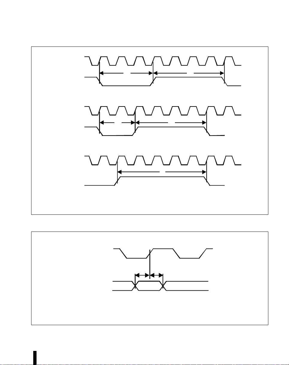
2.4. Clock, Reset, ISA Bus, X-Bus and Host Timing Diagrams
PCICLK,
SYSCLK,
OSC
Figure 1. Test Load
Period
High Time
2.0V
0.8V
Low Time
Fall Time Rise Time
CLK_TM
Figure 2. Clock Timing
29

82371AB (PIIX4) PCI ISA IDE XCELERATOR TIMING SPECIFICATIONS E
PRELIMINARY
SUS_STAT[1:2]#
PCIRST#, RSTDRV
CPURST, PCIRST#,
RSTDRV
(Write to RC Register)
t2f
Active Inactive
t2h
InactiveActiveCPURST
reset2.vsd
Figure 3. Reset Inactive Timing
t2g
Active
048821_2.vsd
Figure 4. Reset Active Pulse Width
30
E 82371AB (PIIX4) PCI ISA IDE XCELERATOR TIMING SPECIFICATIONS
PRELIMINARY
PCIC LK
t3b
SMI#
PCIC LK
t3c
EXTSMI#
PCIC LK
STP C LK#
t3d
Figure 5. SMI#, EXTSMI# and STPCLK# Timing
PC ICLK
t3f
EXTSMI#
t3e
t3i
t3g
048823.drw (M)
Figure 6. Input to PCICLK Setup/Hold Times
0 48 8 24. drw (M )
31

82371AB (PIIX4) PCI ISA IDE XCELERATOR TIMING SPECIFICATIONS E
PRELIMINARY
PC ICL K
t3a,t3h
SMI#, EXTSMI#,
STPCLK#
BALE
LA[23:17]
SA[19:0], SBHE#
MEMR#, MEMW#
SMEMx#
MEMCS16#
ZEROWS#
IOCHRDY
SD[7:0] R
SD[7:0] W
04 88 25.drw (M )
Figure 7. HCLKIN to Output Valid Delay
t4a
t5a
t6d
t5d
t6c
t8a
t11b
t13f
t13d
t13b
t15b
t10a
t9a
t5b
t7d, t7e
t5f
t4b
t6e
t7g
t8a
t7it15e
t9c, t9d
t9b
t10d
t10b,t10c
32
048826_2.vsd
Figure 8. 8-Bit ISA Memory Slave Timing (PIIX4 as Master)

E 82371AB (PIIX4) PCI ISA IDE XCELERATOR TIMING SPECIFICATIONS
PRELIMINARY
t4a
BALE
LA[23:17]
SA[15:0],SBHE#
MEMR#, MEMW#
SMEMW#, SMEMR#
MEMCS16#
ZEROWS#
IOCHRDY
SD[15:0] R
SD[15:0] W
t11a
t5a
t5c
t11d
t13e
t6d
t6a
t13c
t10a
t8a
t13a
t15a
t7a, t7c
t15e
t5e
t5b
t7i
t9b
t6e
t4b
t7f
t8a
t11c
t9c, t9d
t10b, t10c
t10d
048827_2.vsd
Figure 9. 16-Bit ISA Memory Slave Timing (PIIX4 as Master)
33

82371AB (PIIX4) PCI ISA IDE XCELERATOR TIMING SPECIFICATIONS E
PRELIMINARY
AEN
t14a
t14b
t4a
BALE
t6d
SA[19:0], SBHE#
t14c
t6e
IOR#, IOW#
IOCS16#
ZEROWS#
IOCHRDY
SD[7:0] R
SD[7:0] W
t6c
t12b
t13f
t13b
t15b t15e
t10a
t9a
t7d, t7e
t9b
t7i
t9c,t9d
t10b, c
Figure 10. 8-Bit ISA I/O Slave Timing (PIIX4 as Master)
t4b
t7h
t10d
048828_2.vsd
34

E 82371AB (PIIX4) PCI ISA IDE XCELERATOR TIMING SPECIFICATIONS
PRELIMINARY
AEN
BALE
SA[19:0], SBHE#
IOR#, IOW#
IOCS16#
IOCHRDY
SD[15:0] R
SD[15:0] W
t14b
t6d
t14a
t12a
t6b
t4a
t10a
t15a
t12d
t15e
t7b
t9a
t14c
t6e
t4b
t7h
t12c
t7i
t9d,
t9c
t10d
t10b, c
048829_2.vsd
Figure 11. 16-Bit I/O Slave Timing (PIIX4 as Master)
35

82371AB (PIIX4) PCI ISA IDE XCELERATOR TIMING SPECIFICATIONS E
PRELIMINARY
BALE
LA[23:17]
t17a
SA[19:0], SBHE#
MEMR#, MEMW#
IOCHRDY
MEMCS16#
SD[7:0] R
SD[7:0] W
t21a
t16a
t20a
t22a
t22c
t18a
t21b,
t21c
t22b
t19a
t19c,
t19d
t20b
t17c
t18c
048830_2.vsd
36
Figure 12. ISA Master Accessing PCI Memory Timing

E 82371AB (PIIX4) PCI ISA IDE XCELERATOR TIMING SPECIFICATIONS
PRELIMINARY
AEN
Low
BALE
SA[19:0], SBHE#
IOR#, IOW#
IOCHRDY
SD[7:0] R
SD[7:0] W
High
t17b
t22a t22c
t20a
Figure 13. ISA Master Accessing PIIX4 Register Timing
t19b
t18b
t22b
t19a
t17c
t19c,
t19d
t20b
t18d
048831.drw
SERR#,
IOCHK#
t23a
NMI
048832.vsd
Figure 14. NMI Timing
37

82371AB (PIIX4) PCI ISA IDE XCELERATOR TIMING SPECIFICATIONS E
PRELIMINARY
IRQx
DREQ
DACK#
AE N
SD [1 5: 0]
SA [1 5: 0]
LA [23:19]
BH E #
ME M R #, ME M W #
IO R# , IO W#
t24a
Figure 15. Interrupt Timing
t27a
048833.vsd
t2 6a
t27b
ME M R #, M E M W#
SM E M R#, SM EM W #
38
t28 a t2 8b
0 4 883 4_2.vsd
Figure 16. ISA Master Miscellaneous Timing

E 82371AB (PIIX4) PCI ISA IDE XCELERATOR TIMING SPECIFICATIONS
PRELIMINARY
SD[7:0]
SD[15:8]
IOR#, IOW#
MEMR#, MEMW#
SD[7:0] or SD[15:8]
t29a
t29c
t29b
IOR#, MEMR#, OR
SMEMR#
SD[7:0] or SD[15:8]
IOW#, MEMW#, OR
SMEMW#
SD[7:0] or SD[15:8]
t29d
t29e
048835_2.vsd
Figure 17. ISA Master Data Swap Timing
39

82371AB (PIIX4) PCI ISA IDE XCELERATOR TIMING SPECIFICATIONS E
PRELIMINARY
DREQ
t32a
AEN
t31b
DACK#
LA[23:17]
t30b
t32b
t31d
SA[15:0]
IOCHRDY
IOW#
MEMR#
SMEMR#
SD[15:0]
TC
t33a
t34
g
t35a
t34
t34b
t34j
t35a
t37b
t34d
t33
b
a
t40b t40c
Figure 18. DMA Compatible Timing (Memory Read)
t37a
t39a
t34h
t39b
t39h
048836_2.vsd
40

E 82371AB (PIIX4) PCI ISA IDE XCELERATOR TIMING SPECIFICATIONS
PRELIMINARY
DYDREQ
AEN
DACK#
LA[23:17]SA[19:0]IOCHRIOR#MEMW#SMEMW#SD[15:0]TC
t30a
t32a
t31a
t33a
t35a
t34a
t35at34c
t34e
t36a
t39at39bt36b,t36ct40bt40ct34jt34it34ft33bt31ct32b
04883
7
t39
h
Figure 19. DMA Compatible Timing (Memory Write)
41

82371AB (PIIX4) PCI ISA IDE XCELERATOR TIMING SPECIFICATIONS E
PRELIMINARY
SD[7:0]
t38a
SD[15:8]
t38b
IOR#,
MEMR#
t38c
SD[7:0], or
SD[15:8]
Figure 20. DMA Compatible Timing (Data Swap)
t38d
048838.vsd
42

E 82371AB (PIIX4) PCI ISA IDE XCELERATOR TIMING SPECIFICATIONS
PRELIMINARY
DREQ
AEN
DACK#
IOW#
MEMR#
SD[15:0]
IOR#
MEMW#
SD[15:0]
TC
t57a
t56b
t57a
t56a
t59a
t58b
t55a
t55b
t60a
t60b
t59c,
t59b
t58d
t58c
t58a
t61b
t61a
t57b
t57b
t56d
t56c
t61c
t61c
dma_f2.vsd
Figure 21. DMA Type F Timing
43

82371AB (PIIX4) PCI ISA IDE XCELERATOR TIMING SPECIFICATIONS E
PRELIMINARY
AEN
BALE
REFRESH#
SA[15:0]
MEMR#
SMEMR#
IOCHRDY
t62a
t64a
t63a
t65d
t66a,b
t65a
t66c
t65c
t62c
Figure 22. PIIX4-Initiated Refresh Timing
t63b
t62b
t62d
t64b
t65b
t65d
048839_2.vsd
44

E 82371AB (PIIX4) PCI ISA IDE XCELERATOR TIMING SPECIFICATIONS
PRELIMINARY
AEN
t63a
t63b
BALE
REFRESH#
SA[15:0]
MEMR#
SMEMR#
IOCHRDY
High
t62a
t62c
t64a
t67a
t65d
t66a,b
Figure 23. ISA Master-Initiated Refresh Timing
t62b
t62d
t64bt65a
t64c
t65b
t65d
t66c t65c
048840_2.vsd
45

82371AB (PIIX4) PCI ISA IDE XCELERATOR TIMING SPECIFICATIONS E
PRELIMINARY
BALE
LA[23:17]
SA[16:0]
PCCS[1:4]#, KBCS#,
MCCS#, RTCCS#
t68a
t68b
MEMR#, MEMW#,
IOR#, IOW#
BIOSCS#, XOE#
XDIR#
SA[16:0]
SA[16:0]
XOE#
XDIR#
t69b
PIIX4 as Master
t69a t69c
t69a
t69b
t69c
ISA Master
Figure 24. PIIX4 and ISA Master Access to X-Bus Timing
t69d
t69f
t69g
t69i
048841.vsd
46

E 82371AB (PIIX4) PCI ISA IDE XCELERATOR TIMING SPECIFICATIONS
PRELIMINARY
FERR#
IRQ13
IOW#
(Write to F0h)
IGNNE#
IRQ12/M,
IRQ1
t73a
t73b
t71a
048844.vsd
IOW#
RTCALE
Figure 25. Coprocessor Error and Mouse Support Timing
t75b
Figure 26. Real Time Clock Timing (RTCALE Generation)
t75a
048845.vsd
47

82371AB (PIIX4) PCI ISA IDE XCELERATOR TIMING SPECIFICATIONS E
PRELIMINARY
OSC
t76a
SPKR
048846.vsd
Figure 27. Speaker Timing
2.5. PCI Timing Diagrams
48
Input
Output
VT
Propagation Delay
VT
prop_del.vsd
Figure 28. Propagation Delay

E 82371AB (PIIX4) PCI ISA IDE XCELERATOR TIMING SPECIFICATIONS
PRELIMINARY
Clock
Output
Clock
1.5V
Valid Delay
VT
val_del.vsd
Figure 29. Valid Delay From Rising Clock Edge
1.5V
Hold TimeSetup Time
VTInput
Figure 30. Setup and Hold Times
VT
sethold.vsd
49

82371AB (PIIX4) PCI ISA IDE XCELERATOR TIMING SPECIFICATIONS E
PRELIMINARY
Input
Output
Figure 31. Float Delay
Pulse Width
VT
Figure 32. Pulse Width
VT
Float
Delay
floatdel.vsd
VT
pulsewid.vsd
50
Clock
Output
1.5V
Output
Enable
Delay
Figure 33. Output Enable Delay
VT
outendel.vsd

E 82371AB (PIIX4) PCI ISA IDE XCELERATOR TIMING SPECIFICATIONS
PRELIMINARY
2.6. IDE Timing Diagrams
PCICLK
t103,t105
t119
DIOx#
DD[15:0] Write
DD[15:0] Read
IORDY
t103,t105
t118
t115 t115
write data
t115b
t115a
read data
t117
t116
sample point
t117a
t120
t106,t107 t106,t107
DA[2:0], CS1#, CS3#
idepio_2.vsd
Figure 34. IDE PIO Mode
51

82371AB (PIIX4) PCI ISA IDE XCELERATOR TIMING SPECIFICATIONS E
PRELIMINARY
PCICLK
t114b
DDREQ[1:0]
DDACK[1:0]
DIOx#
t114a
t113
t102,t104 t103,t105
t119
t115a
t120
t115b
DD[15:0] Read
DD[15:0] Write
Read Data
t115
t115
Write Data
Figure 35. IDE Multiword DMA Mode
Read Data
Write Data
idedma.vsd
52

E 82371AB (PIIX4) PCI ISA IDE XCELERATOR TIMING SPECIFICATIONS
PRELIMINARY
Full Speed: 4 to 20 ns at CL=50 pF
Differential
Data Lines
90%
10%
10%
90%tRtF
Rise Time
Fall Time
Los Speed: 75 ns at CL=50 pF, 300 ns at CL=350 pF
CLC
L
2.7. USB Timing Diagrams
Tperiod
Differential
Data Lines
USB_1.vsd
Figure 36. Data Signal Rise and Fall Time
Crossover
Points
Consecutive
Transitions
Paired
Transitions
USB_2.vsd
Figure 37. Data Jitter
53

82371AB (PIIX4) PCI ISA IDE XCELERATOR TIMING SPECIFICATIONS E
PRELIMINARY
Tperiod
Data
Differential
Data Lines
Crossover
Level
EOP
Width
USB_3.vsd
Figure 38. EOP Width Timing
2.8. IOAPIC Timing Diagrams
54
SA[19:0]
APICCS#
MEMx#
t137
t136
Figure 39. PIIX4 to IOAPIC Timing
apic_01.vsd

E 82371AB (PIIX4) PCI ISA IDE XCELERATOR TIMING SPECIFICATIONS
PRELIMINARY
smbusto.vsd
Start
Stop
t148
CLK
ack
CLK
ack
t149
t149
SMB CLK
SMB
2.9. SMBus Timing Diagrams
CLK
Data
t142
t141
t2c
t145
t2d
t2e
t146
Figure 40. SMBus Timing
t143
t2b
t144
smbtm_2.vsd
Figure 41. SMBus Timeout Timing
55

82371AB (PIIX4) PCI ISA IDE XCELERATOR TIMING SPECIFICATIONS E
PRELIMINARY
2.10. Ultra DMA/33 Timing Diagrams
DMARQ (drive)
t164
DMACK# (host)
t162
STOP (host)
DMARDY# (host)
STROBE (drive)
DD[15:0]
DA[2:0], CS[1:0]
t162
t164
udma1.vsd
Figure 42. Ultra DMA/33 Drive Initiating a DMA Burst for a Read Command
56

E 82371AB (PIIX4) PCI ISA IDE XCELERATOR TIMING SPECIFICATIONS
PRELIMINARY
t155
t154
t158
STROBE @ sender
t154
t158
Data @ sender
STROBE @ receiver
Data @ receiver
t159
t156
t157
Figure 43. Ultra DMA/33 Sustained Synchronous DMA Burst
t159
t156
t157
t159
t157
udma2.vsd
57

82371AB (PIIX4) PCI ISA IDE XCELERATOR TIMING SPECIFICATIONS E
PRELIMINARY
t161
udma4.vsd
STROBE (drive)
DMARDY# (host)
DATA (drive)
DMACK# (host)
t164
t160
DMARQ (drive)
CRC
t163
STOP (host)
DMARDY#
STROBE
DATA
udma3.vsd
Figure 44. Ultra DMA/33 Sustained Synchronous DMA Burst
58
Figure 45. Ultra DMA/33 Host Terminating a DMA Burst During a Write Command

UNITED STATES, Intel Corporation
2200 Mission College Blvd., P.O. Box 58119, Santa Clara, CA 95052-8119
Tel: +1 408 765-8080
JAPAN, Intel Japan K.K.
5-6 Tokodai, Tsukuba-shi, Ibaraki-ken 300-26
Tel: + 81-29847-8522
FRANCE, Intel Corporation S.A.R.L.
1, Quai de Grenelle, 75015 Paris
Tel: +33 1-45717171
UNITED KINGDOM, Intel Corporation (U.K.) Ltd.
Pipers Way, Swindon, Wiltshire, England SN3 1RJ
Tel: +44 1-793-641440
GERMANY, Intel GmbH
Dornacher Strasse 1
85622 Feldkirchen/ Muenchen
Tel: +49 89/99143-0
HONG KONG, Intel Semiconductor Ltd.
32/F Two Pacific Place, 88 Queensway, Central
Tel: +852 2844-4555
CANADA, Intel Semiconductor of Canada, Ltd.
190 Attwell Drive, Suite 500
Rexdale, Ontario M9W 6H8
Tel: +416 675-2438
 Loading...