

Page 1

Intel® Xeon® Processor E5-2400
Product Family
Thermal/Mechanical Design Guide
May 2012
Reference Number: 327250-001
Page 2

Legal Lines and Disclaimers
INFORMATION IN THIS DOCUMENT IS PROVIDED IN CONNECTION WITH INTEL® PRODUCTS. NO LICENSE, EXPRESS OR IMPLIED,
BY ESTOPPEL OR OTHERWISE, TO ANY INTELLECTUAL PROPERTY RIGHTS IS GRANTED BY THIS DOCUMENT. EXCEPT AS
PROVIDED IN INTEL'S TERMS AND CONDITIONS OF SALE FOR SUCH PRODUCTS, INTEL ASSUMES NO LIABILITY WHATSOEVER,
AND INTEL DISCLAIMS ANY EXPRESS OR IMPLIED WARRANTY, RELATING T O SALE AND/OR USE OF INTEL PRODUCT S INCLUDING
LIABILITY OR WARRANTIES RELA TING T O FITNES S FOR A PARTICULAR PURPOSE, MERCHANT ABILITY, OR INFRINGEMENT OF ANY
PATENT, COPYRIGHT OR OTHER INTELLECTUAL PROPERTY RIGHT. Intel products are not intended for use in medical, life saving,
life sustaining, critical control or safety systems, or in nuclear facility applications.
Intel may make changes to specifications and product descriptions at any time, without notice.
Designers must not rely on the absence or characteristics of any features or instructions marked “reserved” or “undefined.” Intel
reserves these for future definition and shall have no responsibility whatsoev er for conflicts or incompatibilities arising from future
changes to them.
The Intel® Xeon® E5-2400 Product Family may contain design defects or errors known as errata which may cause the product to
deviate from published specifications. Current characterized errata are available on request.
Requires a system with Intel® Turbo Boost Technology. Intel Turbo Boost Technology and Intel Turbo Boost Technology 2.0 are only
available on select Intel® processors. Consult your PC manufacturer. Performance varies depending on hardware, software, and
system configuration. For more information, visit http://www.intel.com/go/turbo
Contact your local Intel sales office or your distributor to obtain the latest specifications and before placing your product order.
Copies of documents which have an order number and are referenced in this document, or other Intel literature may be obtained
by calling 1-800-548-4725 or by visiting Intel's website at http://www.intel.com.
Intel, Xeon, and the Intel logo are tr ademarks or r egistered tr ad emarks of Intel Corpor ation or its subsidiaries in the United States
and other countries.
*Other names and brands may be claimed as the property of others.
Copyright © 2012, Intel Corporation. All Rights Reserved.
2 Intel® Xeon® Processor E5-2400 Product Family
Thermal/Mechanical Design Guide
Page 3

Contents
1Introduction..............................................................................................................9
1.1 References.......................................................................................................10
1.2 Definition of Terms............................................................................................10
2 LGA1356 Socket ......................................................................................................13
2.1 Board Layout....................................................................................................15
2.2 Attachment to Motherboard................................................................................16
2.3 Socket Components...........................................................................................16
2.3.1 Socket Body Housing..............................................................................16
2.3.2 Solder Balls...........................................................................................16
2.3.3 Contacts ...............................................................................................17
2.3.4 Pick and Place Cover...............................................................................17
2.4 Package Installation / Removal ......... ..................................................................18
2.4.1 Socket Standoffs and Package Seating Plane..............................................19
2.5 Durability.........................................................................................................19
2.6 Markings..........................................................................................................19
2.7 Component Insertion Forces ...............................................................................20
2.8 Socket Size ......................................................................................................20
2.9 LGA1356 Socket NCTF Solder Joints.....................................................................20
3 Independent Loading Mechanism (ILM) and Back Plate...........................................23
3.1 Design Concept.................................................................................................23
3.1.1 ILM Assembly Design Overview.............. .. .. ........................... .. ... ..............23
3.1.2 ILM Back Plate Design Overview...............................................................24
3.1.3 Durability..............................................................................................24
3.2 Assembly of ILM to a Motherboard.......................................................................25
3.3 ILM Cover .............. .. .. ......................... .. .......................... .. ......................... .. .. ..27
4 LGA1356 Socket, ILM and Back Plate Electrical, Mechanical, and Environmental
Specifications29
4.1 Component Mass...............................................................................................29
4.2 Package/Socket Stackup Height ..........................................................................29
4.3 Socket Maximum Temperature............................................................................29
4.4 Loading Specifications.................................... .. .. .. ......................... .. .. .................30
4.5 Electrical Requirements......................................................................................30
4.6 Environmental Requirements .................................................................. ............31
5Thermal Solutions...................................................................................................33
5.1 Boundary Conditions..........................................................................................33
5.2 Assembly .........................................................................................................35
5.2.1 Thermal Interface Material (TIM)..............................................................36
5.3 Structural Considerations ...................................................................................36
5.4 Thermal Design.................................................................................................36
5.4.1 Thermal Characterization Parameter.........................................................36
5.5 Fan Speed Control.............................................................................................37
5.5.1 Fundamentals........................................................................................37
5.6 Thermal Features..............................................................................................37
5.6.1 TCONTROL and DTS Relationship..............................................................38
5.6.2 Short Duration TCC Activation and Catastrophic Thermal
Management for Intel® Xeon® Processor E5-2400 Product Family....... ......... 39
5.6.3 Intel® Turbo Boost Technology................................................................40
5.7 Thermal Guidance .............................................................................................40
5.7.1 Thermal Excursion..................................................................................40
5.7.2 Absolute Processor Temperature ..............................................................40
Intel® Xeon® Processor E5-2400 Product Family 3
Thermal/Mechanical Design Guide
Page 4

5.8 DTS Based Thermal Specification.........................................................................41
5.8.1 Compliance to Tcase Based Thermal Profile................................................41
5.8.2 Considerations for Follow-on Processor ......................................................41
5.8.3 DTS Based Thermal Profile, Tcontrol and Margin
for the Intel® Xeon® Processor E5-2400 Product Family .............................41
5.8.4 Power Calculation for the Intel® Xeon® Processor E5-2400 Product Family....42
5.8.5 Averaging the DTS Based Thermal Specification for the
5.8.6 Capabilities for the Follow-on Processor .....................................................43
6 Quality and Reliability Requirements .......................................................................45
6.1 Test Conditions .................................................................................................45
6.2 Intel Reference Component Validation ..................................................................45
6.2.1 Board Functional Test Sequence ...............................................................45
6.2.2 Post-Test Pass Criteria.............................................................................45
6.2.3 Recommended BIOS/Processor/Memory Test Procedures .............................46
6.3 Material and Recycling Requirements....................................................................46
A Component Su ppliers...............................................................................................47
A.1 Intel Enabled Supplier Information.......................................................................47
A.1.1 Intel Reference Thermal Solution..............................................................47
A.1.2 Intel Collaboration Thermal Solution..........................................................47
A.1.3 Alternative Thermal Solution ....................................................................48
A.1.4 Socket, ILM and Back Plate......................................................................50
B Mechanical Drawings ...............................................................................................51
C Socket Mechanical Drawings....................................................................................85
D Processor Installation Tool ......................................................................................91
E Embedded Thermal Solutions...................................................................................93
E.1 Performance Targets.................................................. ........................................93
E.2 Thermal Design Guidelines................................ .. ........................... .. ...................94
E.2.1 High Case Temperature Thermal Profile.....................................................94
E.3 Mechanical Drawings and Supplier Information......................................................95
Intel® Xeon® Processor E5-2400 Product Family........................................42
Figures
1-1 Intel® Xeon® Processor E5-2400 Product Family Platform Socket Stack ...... .. .. .. .. ...... 9
2-1 LGA1356 Socket with Pick and Place Cover Removed..............................................13
2-2 LGA1356 Socket Contact Numbering (Top View of Socket) ......................................14
2-3 LGA1356 Socket Land Pattern (Top View of Board).................................................15
2-4 Attachment to Motherboard................ .. .. ........................... ..................................16
2-5 Pick and Place Cover............................. .. .. ................................................... .. .. ..17
2-6 Package Installation / Removal Features...............................................................18
2-7 Package and Board Enabling Mark (-2) .................................................................19
2-8 LGA1356 NCTF Solder Joints ...............................................................................21
3-1 ILM Assembly....................................................................................................24
3-2 Back Plate ........................................................................................................25
3-3 ILM Assembly....................................................................................................26
3-4 Pin1 and ILM Lever ............................................................................................27
4-1 Flow Chart of Knowledge-Based Reliability Evaluation Methodology...........................32
5-1 Best-fit Equations ..............................................................................................34
5-2 1U Reference Heatsink Assembly .........................................................................35
5-3 Processor Thermal Characterization Parameter Relationships ...................................37
B-1 Board Keepin / Keep out Zone s (She et 1 of 4)................................... .. .. .. ...............52
4 Intel® Xeon® Processor E5-2400 Product Family
Thermal/Mechanical Design Guide
Page 5

B-2 Board Keepin / Keepout Zones (Sheet 2 of 4)........................................................53
B-3 Board Keepin / Keepout Zones (Sheet 3 of 4)........................................................54
B-4 Board Keepin / Keepout Zones (Sheet 4 of 4)........................................................55
B-5 1U Reference Heatsink Assembly (Sheet 1 of 2) ....................................................56
B-6 1U Reference Heatsink Assembly (Sheet 2 of 2) ....................................................57
B-7 1U Reference Heatsink Fin and Base (Sheet 1 of 2)................................................58
B-8 1U Reference Heatsink Fin and Base (Sheet 2 of 2)................................................59
B-9 Heatsink Shoulder Screw (1U, 2U and Tower) .......................................................60
B-10 Heatsink Compression Spring (1U, 2U and Tower).................................................61
B-11 Heatsink Retaining Ring (1U, 2U and Tower).........................................................62
B-12 Heatsink Load Cup (1U, 2U and Tower)................................................................63
B-13 2U Collaborative Heatsink Assembly (Sheet 1 of 2)................................................64
B-14 2U Collaborative Heatsink Assembly (Sheet 2 of 2)................................................65
B-15 2U Collaborative Heatsink Volumetric (Sheet 1 of 2) ......................... .. .. .................66
B-16 2U Collaborative Heatsink Volumetric (Sheet 2 of 2) ......................... .. .. .................67
B-17 Tower Collaborative Heatsink Assembly (Sheet 1 of 2) ...........................................68
B-18 Tower Collaborative Heatsink Assembly (Sheet 2 of 2) ...........................................69
B-19 Tower Collaborative Heatsink Volumetric (Sheet 1 of 2)..........................................70
B-20 Tower Collaborative Heatsink Volumetric (Sheet 2 of 2)..........................................71
B-21 1U Reference Heatsink Assembly with TIM (Sheet 1 of 2) .......................................72
B-22 1U Reference Heatsink Assembly with TIM (Sheet 2 of 2) .......................................73
B-23 2U Reference Heatsink Assembly with TIM (Sheet 1 of 2) .......................................74
B-24 2U Reference Heatsink Assembly with TIM (Sheet 2 of 2) .......................................75
B-25 Tower Reference Heatsink Assembly with TIM (Sheet 1 of 2)...................................76
B-26 Tower Reference Heatsink Assembly with TIM (Sheet 2 of 2)...................................77
B-27 25.5 mm Reference Heatsink Assembly (Sheet 1 of 2) ...........................................78
B-28 25.5 mm Reference Heatsink Assembly (Sheet 2 of 2) ...........................................79
B-29 25.5 mm Reference Heatsink Fin and Base (Sheet 1 of 2).......................................80
B-30 25.5 mm Reference Heatsink Fin and Base (Sheet 2 of 2).......................................81
B-31 25.5 mm Reference Heatsink Assembly with TIM (Sheet 1 of 2)...............................82
B-32 25.5 mm Reference Heatsink Assembly with TIM (Sheet 2 of 2)...............................83
C-1 Socket Mechanical Drawing (Sheet 1 of 4)............................................................86
C-2 Socket Mechanical Drawing (Sheet 2 of 4)............................................................87
C-3 Socket Mechanical Drawing (Sheet 3 of 4)............................................................88
C-4 Socket Mechanical Drawing (Sheet 4 of 4)............................................................89
D-1 Processor Installation Tool..................................................................................92
E-1 ATCA Heatsink Performance Curves.............................................. .......................94
E-2 NEBS Thermal Profile.........................................................................................95
E-3 ATCA Reference Heat Sink Assembly (Sheet 1 of 2) ...............................................97
E-4 ATCA Reference Heat Sink Assembly (Sheet 2 of 2) ...............................................98
E-5 ATCA Reference Heatsink Fin and Base (Sheet 1 of 2)............................................99
E-6 ATCA Reference Heatsink Fin and Base (Sheet 2 of 2).......................................... 100
Tables
1-1 Reference Documents..................................................................... .. .................10
1-2 Terms and Descriptions......................................................................................10
4-1 Component Mass...............................................................................................29
4-2 1356-land Package and LGA1356 Socket Stackup Height........................................29
4-3 Socket and ILM Mechanical Specifications.............................................................30
4-4 Electrical Requirements for LGA1356 Socket ......................................................... 31
5-1 Values Used to Generate Processor Thermal Specifications......................................33
5-2 Performance Expectations in Compact Electronics Bay (CEB)................................... 34
Intel® Xeon® Processor E5-2400 Product Family 5
Thermal/Mechanical Design Guide
Page 6

5-3 TCONTROL and DTS Relationship.........................................................................38
5-4 Sign Convention................................................................................................38
5-5 T
CONTROL
Relief for Intel® Xeon® Processor E5-2400 Product Family........................39
5-6 Averaging Coefficients........................................................................................43
A-1 Suppliers for the Intel Reference Thermal Solution.................................................47
A-2 Suppliers for the Intel Collaboration Thermal Solution.............................................48
A-3 Suppliers for the Alternative Thermal Solution .......................................................48
A-4 LGA135 6 Socket, ILM and Back Plate........................................................ ............50
B-1 Mechanical Drawing List......................................................................................51
C-1 Mechanical Drawing List......................................................................................85
E-1 8-Core/6-Core Processor Reference Thermal Boundary Conditions............................93
E-2 4-Core Processor Reference Thermal Boundary Conditions.......................................93
E-3 Embedded Heatsink Component Suppliers.............................................................95
E-4 Mechanical Drawings List....................................................................................96
6 Intel® Xeon® Processor E5-2400 Product Family
Thermal/Mechanical Design Guide
Page 7
Revision History
Document
Number
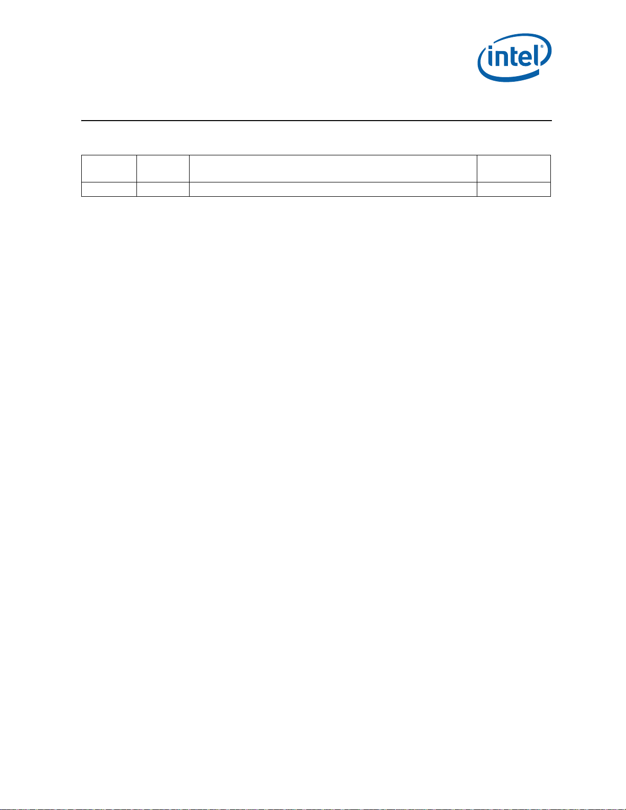
327250 -001 • Initial release of the document. May 2012
Revision
Number
Description Date
§
Intel® Xeon® Processor E5-2400 Product Family 7
Thermal/Mechanical Design Guide
Page 8

8 Intel® Xeon® Processor E5-2400 Product Family
Thermal/Mechanical Design Guide
Page 9
Introduction
1 Introduction
This document provides guidelines for the design of thermal and mechanical solutions
for server and workstation processors in the Intel® Xeon® Processor E5-2400 Product
Family platform. The processors covered include those listed in the Intel® Xeon®
Processor E5-2400 Product Family Datasheet - Volume One. The components described
in this document include:
• The processor thermal solution (heatsink) and associated retention hardware.
• The LGA1356 socket, the Independent Loading Mechanism (ILM) and back plate.
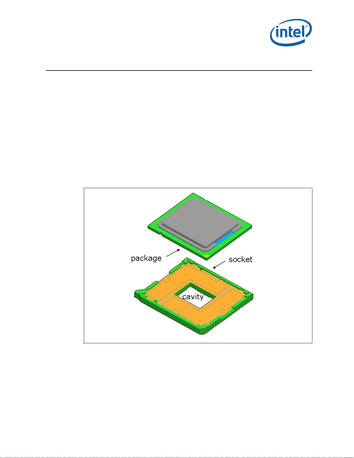
Figure 1-1. Intel® Xeon® Processor E5-2400 Product Family Platform Socket Stack
The goals of this document are:
• To assist board and system thermal mechanical designers.
• To assist designers and suppliers of processor heatsinks.
Thermal profiles and other processor specifications are provided in the appropriate
Datasheet.
Intel® Xeon® Processor E5-2400 Product Family 9
Thermal/Mechanical Design Guide
Page 10
1.1 References
Material and concepts available in the following documents may be beneficial when
reading this document.
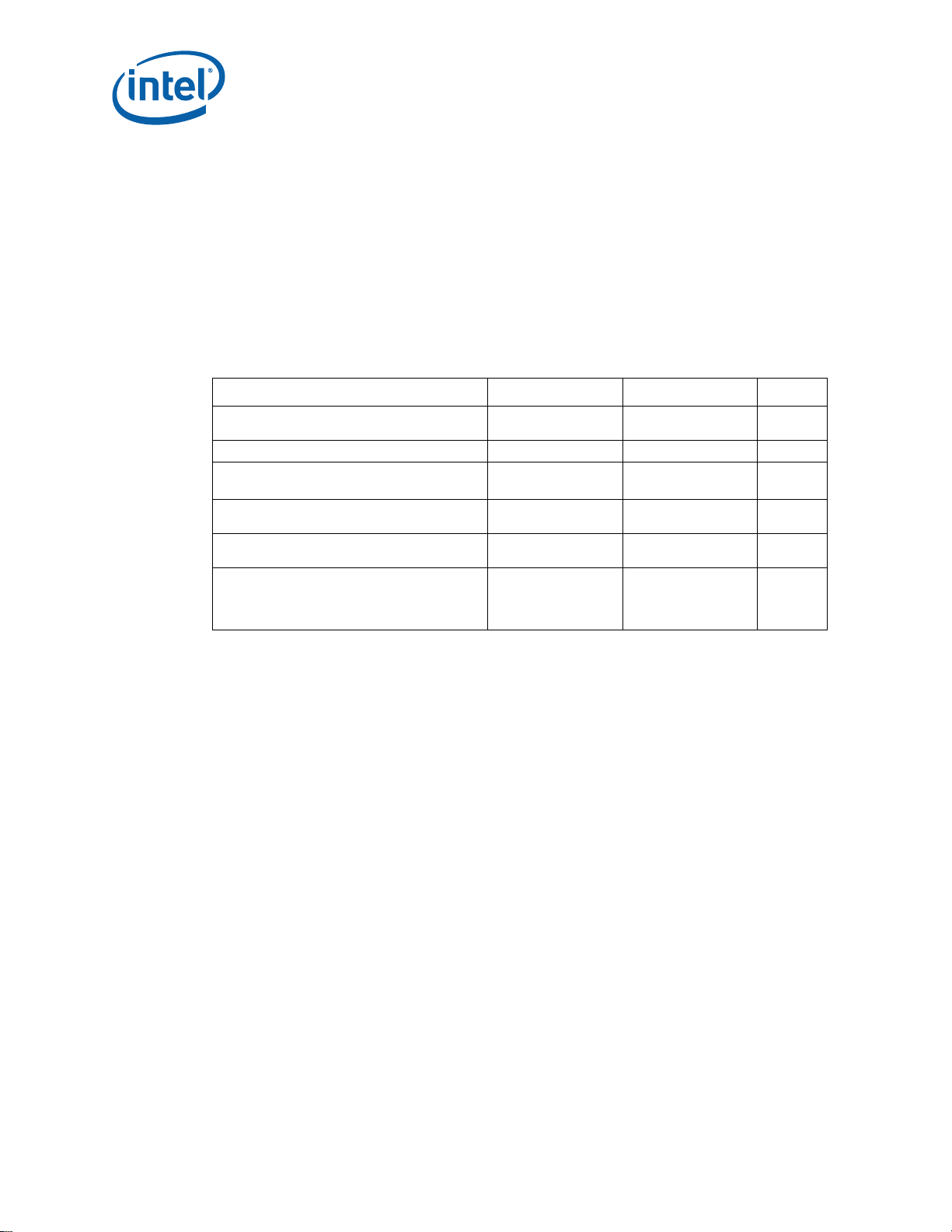
Table 1-1. Reference Documents
Document Number Notes
European Blue Angel Recycling Standards 2
Intel® Xeon® Processor E5-2400 Product Family Datasheet -
Volume One
Platform Environment Control Interface (PECI) Specification 4
Intel® Xeon® Processor E5-2400 Processor Product Family
Mechanical Model
Intel® Xeon® Processor E5-2400 Processor Product Family
Thermal Model
Manufacturing With Intel Components Using Lead-Free
Technology
Platform Digital Thermal Sensor (DTS) Based Thermal
Specifications and Overview
Notes:
1. Available at http://www.intel.com. Document numbers are subject to change.
2. Available at http://www.blauer-engel.de/en/index.php
3. Available at https://learn.intel.com/portal/scripts/general/logon.aspx.
4. Contact your local Intel Field Sales Representative.
Introduction
327248 1
327322 1
327321 1
3
4
1.2 Definition of Terms
Table 1-2. Terms and Descriptions (Sheet 1 of 2)
Term Description
Bypass Bypass is the area between a passive heatsink and any object that can act to form a
DTS Digital Thermal Sensor reports a relative die temperature as an offset from TCC
FSC Fan Speed Control
IHS Integrated Heat Spreader: a component of the processor pac k age used to enhance the
ILM Independent Loading Mechanism provides the force needed to seat the 1356-LGA land
LGA1356 socket The processor mates with the system board through this surface mount, 1356-contact
PECI The Platform Environment Control Interface (PECI) is a one- wire in terface that pro vides
Ψ
CA
Ψ
CS
Ψ
SA
duct. For this example, it can be expressed as a dimension away from the outside
dimension of the fins to the nearest surface.
activation temperature.
thermal performance of the package. Component thermal solutions interface with the
processor at the IHS surface.
package onto the socket contacts.
socket.
a communication channel between Intel processor and chipset components to external
monitoring devices.
Case-to-ambient thermal characterization parameter (psi). A measure of thermal
solution performance using t otal package power. Defined as (T
Package Power. Heat source should always be specified for Ψ measurements.
Case-to-sink thermal characterization parameter. A measure of thermal interface
material performance using total package po wer. Defined as (T
Package Power.
Sink-to-ambient thermal characterization parameter. A measure of heatsink thermal
performance using total package power. Defined as (T
– TLA) / Total
CASE
– TS) / Total
CASE
– TLA) / Total Package Power.
S
10 Intel® Xeon® Processor E5-2400 Product Family
Thermal/Mechanical Design Guide
Page 11
Introduction
Table 1-2. Terms and Descriptions (Sheet 2 of 2)
Term Description
T
CASE
T
CASE_MAX
TCC Thermal Control Circuit: Thermal monitor uses the TCC to reduce the die temperature
T
CONTROL
TDP Thermal Design Power: Thermal solution should be designed to dissipate this target
Thermal Monitor A power reduction feature designed to decrease temperature after the processor has
Thermal Profile Line that defines the temperature specification of a processor at a given power level.
TIM Thermal Interface Material: The thermally conductive compound between the heatsink
T
LA
T
SA
U A unit of measure used to define server rack spacing height. 1U is equal to 1.75 in, 2U
The case temperature of the p rocessor measure d at the geomet ric center of the topside
of the IHS.
The maximum case temperature as specified in a component specification.
by using clock modulation and/or operating frequency and input voltage adjustment
when the die temperature is very near its operating limits.
T
control.
is a static value below TCC activation used as a trigger point for fan speed
CONTROL
power level. TDP is not the maximum power that the processor can dissipate.
reached its maximum operating temperature.
and the processor case. This material fills the air gaps and voids, and enhances the
transfer of the heat from the processor case to the heatsink.
The measured ambient temperature locally surrounding the proces sor. The ambient
temperature should be measured just upstream of a p assive he atsink or at the fan inle t
for an active heatsink.
The system ambient air temperature external to a system chassis. This temperature is
usually measured at the chassis air inlets.
equals 3.50 in, etc.
§
Intel® Xeon® Processor E5-2400 Product Family 11
Thermal/Mechanical Design Guide
Page 12

Introduction
12 Intel® Xeon® Processor E5-2400 Product Family
Thermal/Mechanical Design Guide
Page 13
LGA1356 Socket
2 LGA1356 Socket
This chapter describes a surface mount, LGA (Land Grid Array) socket intended for
processors in the E5-2400 Product Family Platform. The socket provides I/O , power and
ground contacts. The socket contains 1356 contacts arrayed about a cavity in the
center of the socket with lead-free solder balls for surface mounting on the
motherboard.
The socket has 1356 contacts with 1.016 mm X 1.016 mm pitch (X by Y) in a 43x41
grid array with 21x17 grid depopulation in the center of the array and selective
depopulation elsewhere.
The socket must be compatible with the package (processor) and the Independent
Loading Mechanism (ILM). The design includes a back plate which is a key contributor
in producing a uniform load on the socket solder joints. Socket loading specifications
are listed in Section 4.4.
Figure 2-1. LGA1356 Socket with Pick and Place Cover Removed
Intel® Xeon® Processor E5-2400 Product Family 13
Thermal/Mechanical Design Guide
Page 14
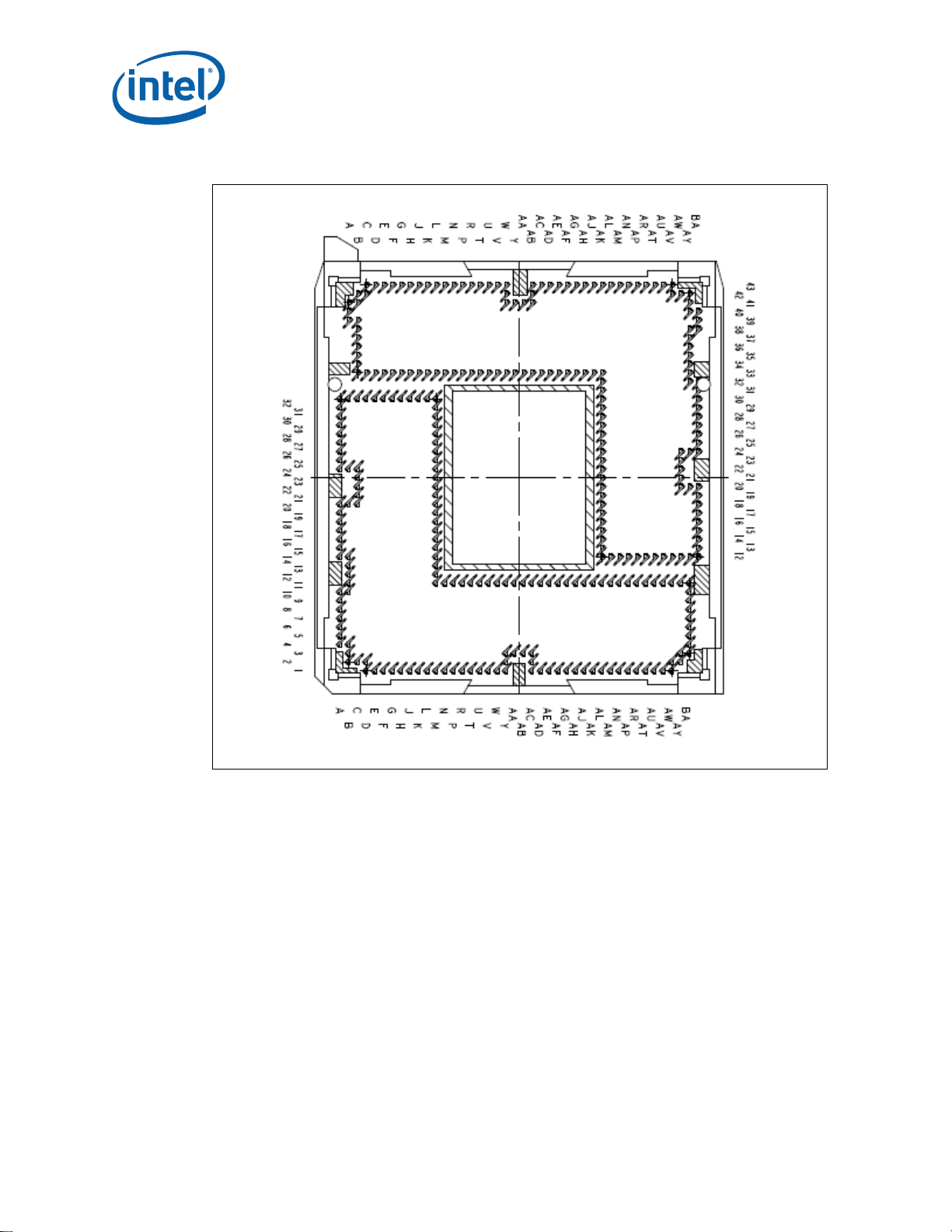
Figure 2-2. LGA1356 Socket Contact Numbering (Top View of Socket)
LGA1356 Socket
14 Intel® Xeon® Processor E5-2400 Product Family
Thermal/Mechanical Design Guide
Page 15
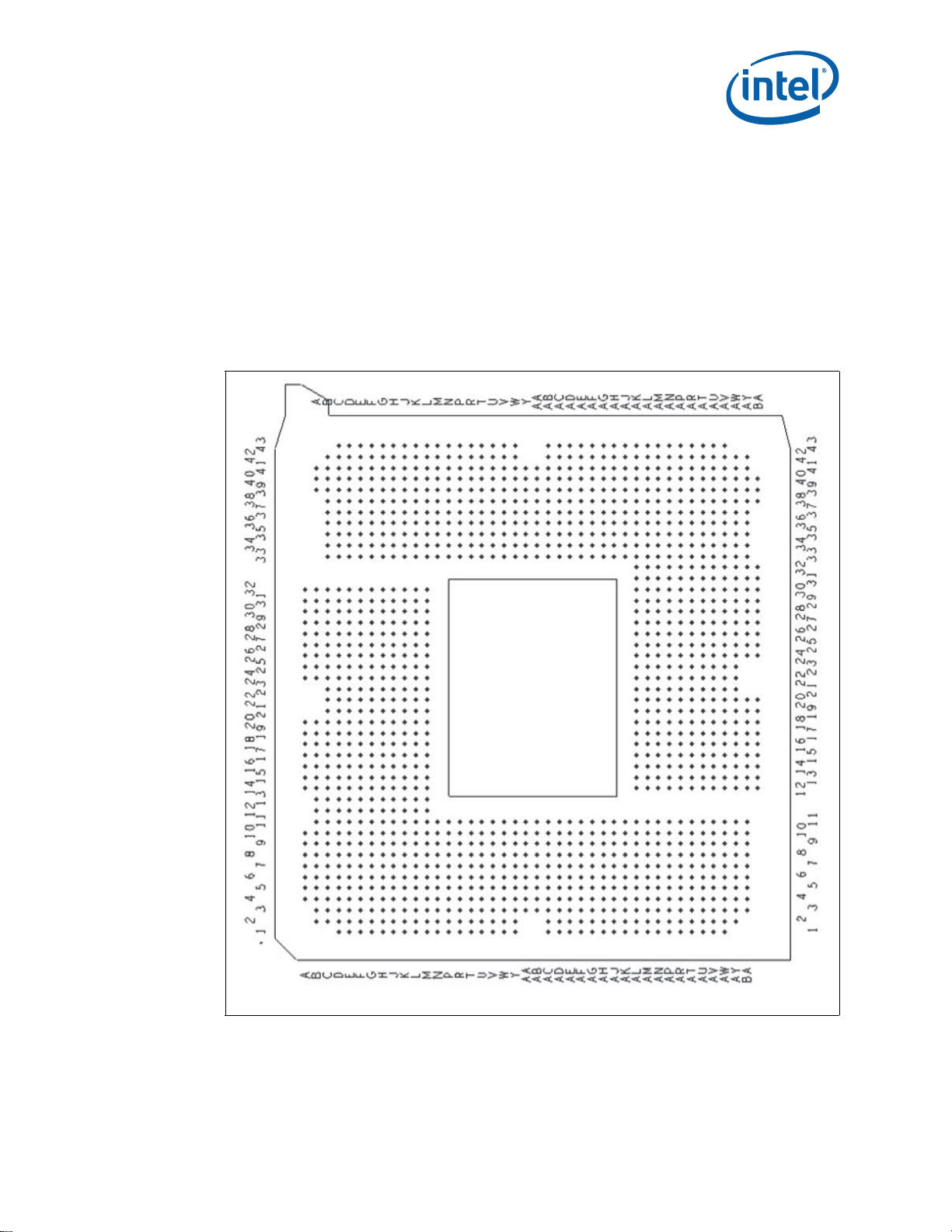
LGA1356 Socket
2.1 Board Layout
The land pattern for the LGA1356 socket is 40 mils X 40 mils (X by Y). Note that there
is no round-off (conversion) error between socket pitch (1.016 mm) and board pitch
(40 mil) as these values are equivalent.
In general, metal defined (MD) pads perform better than solder mask defined (SMD)
pads under thermal cycling, and SMD pads perform better than MD pads under
dynamic stress. At this time, complete recommendations for pad definition and pad size
do not exist for the LGA1356 socket. See Section 2.9 for more information on pad
definition and pad size.
Figure 2-3. LGA1356 Socket Land Pattern (Top View of Board)
Intel® Xeon® Processor E5-2400 Product Family 15
Thermal/Mechanical Design Guide
Page 16
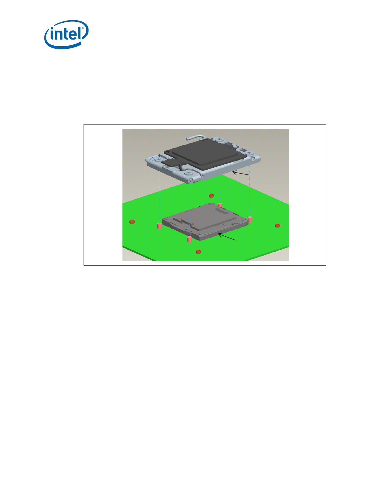
2.2 Attachment to Motherboard
LGA1356
Socket
ILM
The socket is attached to the motherboard by 1356 solder balls. There are no additional
external methods (that is, screw, extra solder, adhesive, and so on) to attach the
socket.
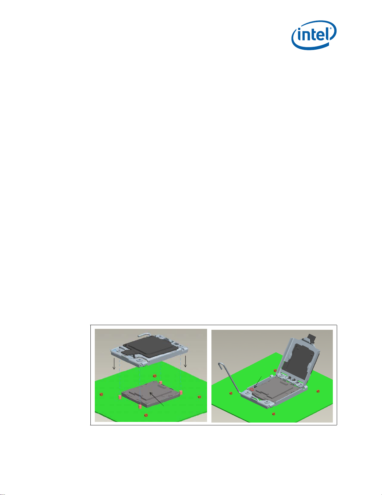
As indicated in Figure 2-4, the Independent Loading Mechanism (ILM) is not present
during the attach (reflow) process.
Figure 2-4. Attachment to Motherboard
LGA1356 Socket
2.3 Socket Components
The socket has two main components, the socket body and Pick and Place (PnP) cover,
and is delivered as a single integral assembly. Refer to Appendix C for detailed
drawings.
2.3.1 Socket Body Housing
The housing material is thermoplastic or equivalent with UL 94 V -0 flame rating capable
of withstanding 260 °C for 40 seconds (typical reflow/rework). The socket coefficient of
thermal expansion (in the XY plane), and creep properties, must be such that the
integrity of the socket is maintained for the conditions listed in the LGA1366 Socket
Validation Reports, and the LGA1356 Addendum.
The color of the housing will be dark as compared to the solder balls to provide the
contrast needed for pick and place vision systems.
2.3.2 Solder Balls
A total of 1356 solder balls corresponding to the contacts are on the bottom of the
socket for surface mounting with the motherboard.
The socket has the following solder ball material:
• Lead free SAC (SnAgCu) solder alloy with a silver (Ag) content between 3% and
4% and a melting temperature of approximately 217 °C. The alloy must be
16 Intel® Xeon® Processor E5-2400 Product Family
Thermal/Mechanical Design Guide
Page 17
LGA1356 Socket
ILM Installation
Pick and
Place Cover
Pin 1
ILM cover
compatible with immersion silver (ImAg) motherboard surface finish and a SAC
alloy solder paste.
The co-planarity (profile) and true position requirements are defined in Appendix C.
2.3.3 Contacts
Base material for the contacts is high strength copper alloy.
For the area on socket contacts where processor lands will mate, there is a 0.381 μm
[15 μinches] minimum gold plating over 1.27 μm [50 μinches] minimum nickel
underplate.
No contamination by solder in the contact area is allowed during solder reflow.
2.3.4 Pick and Place Cover
The cover provides a planar surface for vacuum pick up used to place components in
the Surface Mount Technology (SMT) manufacturing line. The cover remains on the
socket during reflow to help prevent contamination during reflow. The cover can
withstand 260 °C for 40 seconds (typical reflow/rework profile) and the conditions
listed in the LGA1366 Socket Validation Reports, and LGA1356 Addendum, without
degrading. Reports are available from socket suppliers listed in Appendix A.
As indicated in Figure 2-5, the Pick and Place cover remains on the socket during ILM
installation. Use of the ILM cover can mitigate against bent socket contacts associated
with reinstalling the Pick and Place cover. A cover should remain on whenever possible
to help prevent damage to the socket contacts. See Section 3.2 and Section 3.3 for
additional information on the ILM cover.
Pick and Place cover retention must be sufficient to support the socket weight during
lifting, translation, and placement (board manufacturing), and during board and
system shipping and handling.
Pick and Place covers are designed to be interchangeable between socket suppliers. As
indicated in Figure 2-5, a Pin1 indicator on the Pick and Place cover provides a visual
reference for proper orientation with the socket.
Figure 2-5. Pick and Place Cover
Intel® Xeon® Processor E5-2400 Product Family 17
Thermal/Mechanical Design Guide
Page 18
2.4 Package Installation / Removal
As indicated in Figure 2-6, access is provided to facilitate manual installation and
removal of the package.
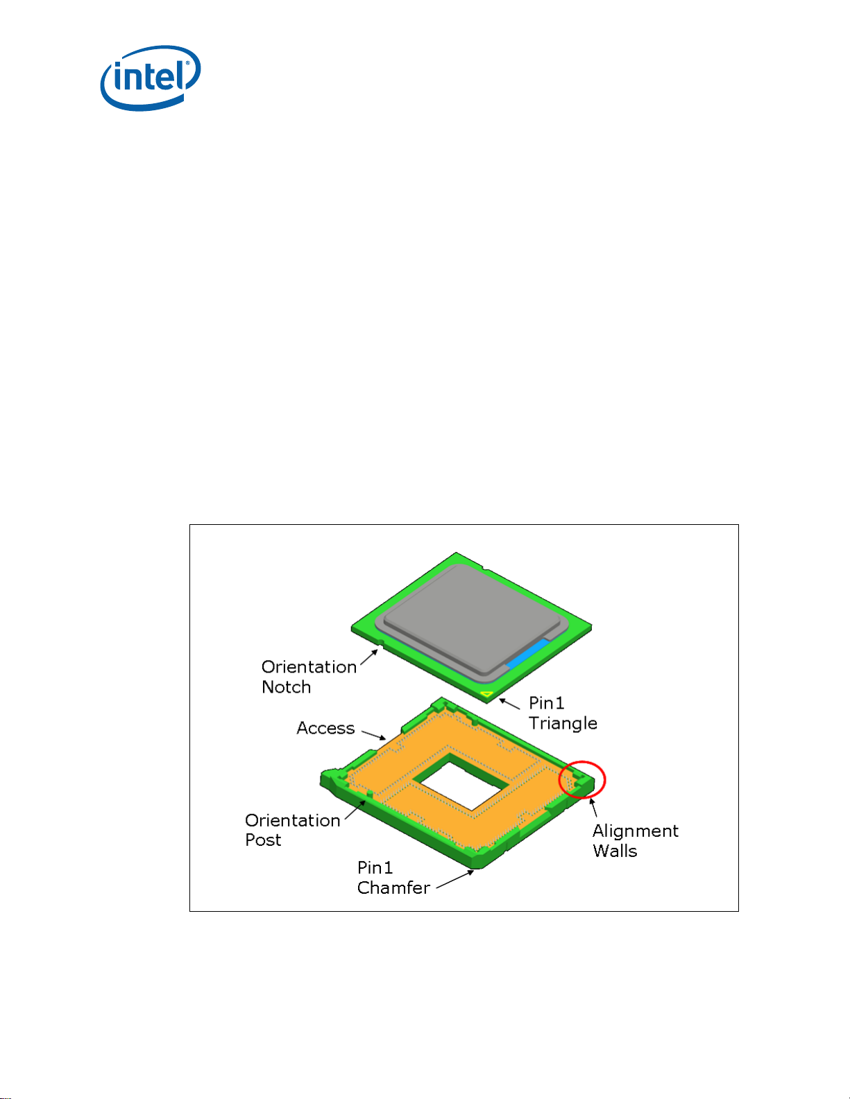
To assist in package orientation and alignment with the socket:
• The package Pin1 triangle and the socket Pin1 chamfer provide visual reference for
proper orientation.
• The package substrate has orientation notches along two opposing edges of the
package, offset from the centerline. The socket has two corresponding orientation
posts to physically prevent mis-orientation of the package. These orientation
features also provide initial rough alignment of package to socket.
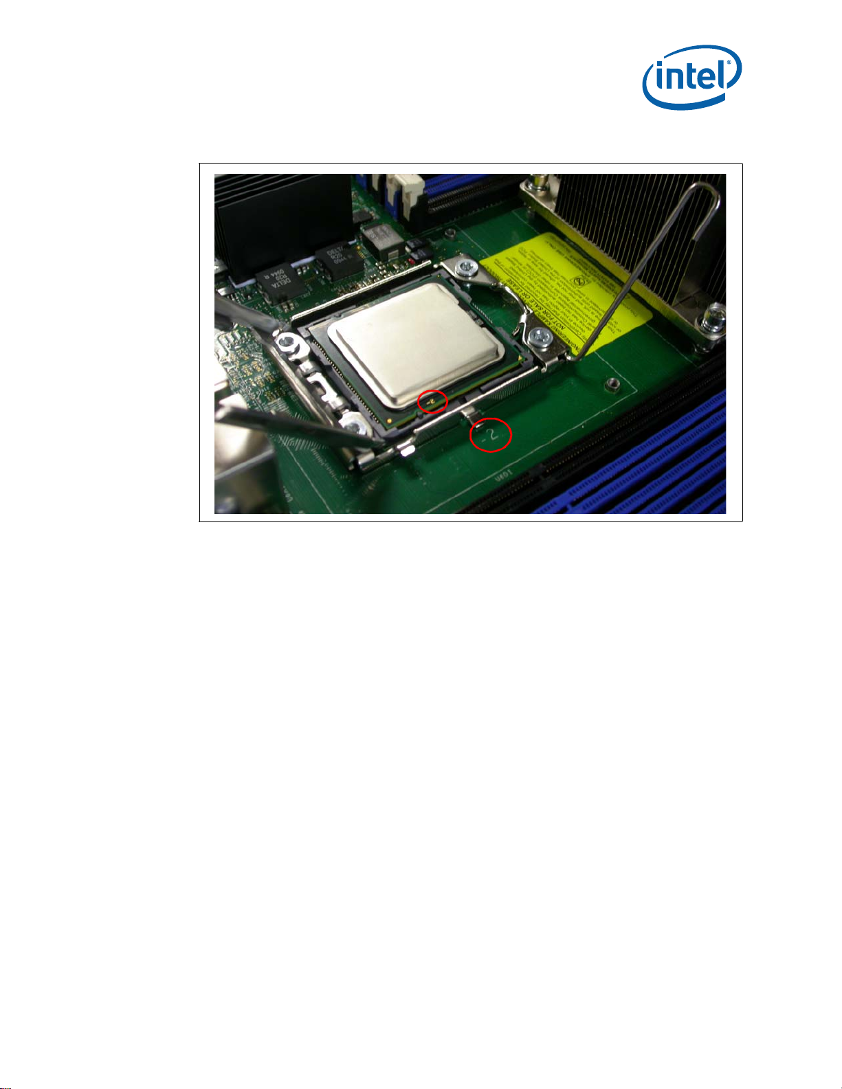
• As shown in Figure 2-7, the package substrate has a “-2” mark near the orientation
notch on the Pin 1 side. Similarly, space has been reserved for a “-2” mark on the
motherboard in the Board Keepin / Keepout Z on es in Figure B-1 and Figure B-2.
These matching marks help prevent system assemblers from installing the
incorrect processor into the socket.
• The socket has alignment walls at the four corners to provide final alignment of the
package.
See Appendix D for information regarding a tool designed to provide mechanical
.
Figure 2-6. Package Installation / Removal Features
assistance during processor installation and removal.
LGA1356 Socket
18 Intel® Xeon® Processor E5-2400 Product Family
Thermal/Mechanical Design Guide
Page 19
LGA1356 Socket
Figure 2-7. Package and Board Enabling Mark (-2)
2.4.1 Socket Standoffs and Package Seating Plane
Standoffs on the bottom of the socket base establish the minimum socket height after
solder reflow and are specified in Appendix C.
Similarly, a seating plane on the topside of the socket establishes the minimum
package height. See Section 3.2 for the calculated IHS height above the motherboard.
2.5 Durability
The socket must withstand 30 cycles of processor insertion and removal. The max
chain contact resistance from Table 4-4 must be met when mated in the 1st and 30th
cycles.
The socket Pick and Place cover must withstand 15 cycles of insertion and removal.
2.6 Markings
There are three markings on the socket:
• LGA1356: Font type is Helvetica Bold - minimum 6 point (2.125 mm).
• Manufacturer's insignia (font size at supplier's discretion).
• Lot identification code (allows traceability of manufacturing date and location).
All markings must withstand 260 °C for 40 seconds (typical reflow/rework profile)
without degrading, and must be visible after the socket is mounted on the
motherboard.
LGA1356 and the manufacturer's insignia are molded or laser marked on the side wall.
Intel® Xeon® Processor E5-2400 Product Family 19
Thermal/Mechanical Design Guide
Page 20

2.7 Component Insertion Forces
Any actuation must meet or exceed SEMI S8-95 Safety Guidelines for Ergonomics/
Human Factors Engineering of Semiconductor Manufacturing Equipment, example T able
R2-7 (Maximum Grip Forces). The socket must be designed so that it requires no force
to insert the package into the socket.
2.8 Socket Size
Socket information needed for motherboard design is given in Appendix C.
This information should be used in conjunction with the reference motherboard keepout
drawings provided in Appendix B to ensure compatibility with the reference thermal
mechanical components.
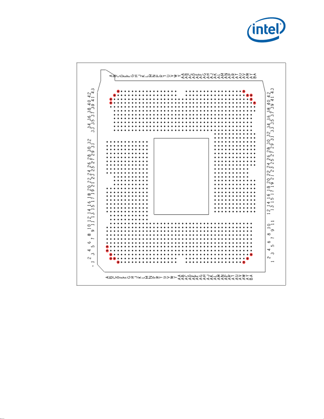
2.9 LGA1356 Socket NCTF Solder Joints
Intel has defined selected solder joints of the socket as non-critical to function (NCTF)
for post environmental testing. The processor signals at NCTF locations are typically
redundant ground or non-critical reserved, so the loss of the solder joint continuity at
end of life conditions will not affect the overall product functionality. Figure 2-8
identifies the NCTF solder joints.
LGA1356 Socket
Since corner pads are often more susceptible to solder joint damage, NCTF locations
are often placed in the corners. When possible, larger pads may be chosen at NCTF
locations to further mitigate against solder joint damage. At this time, complete
recommendations for pad definition and pad size do not exist at NCTF locations. CTF
and NCTF locations are 18mil solder mask defined on Intel reference designs.
20 Intel® Xeon® Processor E5-2400 Product Family
Thermal/Mechanical Design Guide
Page 21
LGA1356 Socket
.
Figure 2-8. LGA1356 NCTF Solder Joints
§
Intel® Xeon® Processor E5-2400 Product Family 21
Thermal/Mechanical Design Guide
Page 22

LGA1356 Socket
22 Intel® Xeon® Processor E5-2400 Product Family
Thermal/Mechanical Design Guide
Page 23

Independent Loading Mechanism (ILM) and Back Plate
3 Independent Loading
Mechanism (ILM) and Back
Plate
The Independent Loading Mechanism (ILM) provides the force needed to seat the
1356-LGA land package onto the socket contacts. The ILM is physically separate from
the socket body. The assembly of the ILM to the board is expected to occur after wave
solder. The exact assembly location is dependent on manufacturing preference and test
flow.
Note: The ILM has two critical functions: deliver the force to seat the processor onto the
socket contacts and distribute the resulting compressive load evenly through the socket
solder joints.
Note: The mechanical design of the ILM is a key contributor to the over all fun ctionality of the
LGA1356 socket. Intel performs detailed studies on integration of processor package,
socket and ILM as a system. These studies directly impact the design of the ILM. The
Intel reference ILM will be “build to print” from Intel controlled drawings. Intel
recommends using the Intel Reference ILM. Custom non-Intel ILM designs do not
benefit from Intel's detailed studies and may not incorporate critical design
parameters.
3.1 Design Concept
The ILM and back plate are assemblies and can be procured from the enabled vendors.
3.1.1 ILM Assembly Design Overview
The ILM assembly consists of four major pieces: load lever, load plate, frame and the
captive fasteners.
The load lever and load plate are stainless steel. The frame and fasteners are high
carbon steel with appropriate plating. The fasteners are fabricated from a high carbon
steel. The frame provides the hinge locations for the load lever and load plate.
The ILM assembly design ensures that once assembled to the back plate and the load
lever is closed, the only features touching the board are the captive fasteners. The
nominal gap of the frame to the board is ~1 mm when the load plate is closed on the
empty socket or when closed on the processor package.
When closed, the load plate applies two point loads onto the IHS at the “dimpled”
features shown in Figure 3-1. The reaction force from closing the load plate is
transmitted to the frame and through the captive fasteners to the back plate. Some of
the load is passed through the socket body to the board inducing a slight compression
on the solder joints.
Intel® Xeon® Processor E5-2400 Product Family 23
Thermal/Mechanical Design Guide
Page 24
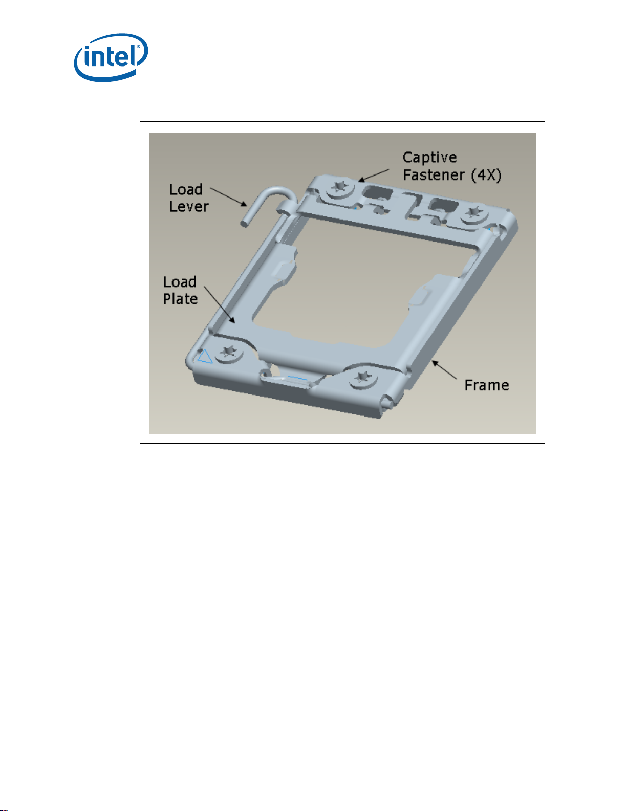
Figure 3-1. ILM Assembly
Independent Loading Mechanism (ILM) and Back Plate
3.1.2 ILM Back Plate Design Overview
The unified back plate consists of a flat steel back plate with threaded studs for ILM
attach, and internally threaded nuts for heatsink attach. The threaded studs have a
smooth surface feature that provides alignment for the back plate to the motherboard
for proper assembly of the ILM around the socket. A clearance hole is located at the
center of the plate to allow access to test points and backside capacitors. An additional
cut-out on two sides provides clearance for backside voltage regulator components. An
insulator is pre-applied. To stay within the temperature limit of the insulator, remove
the back plate prior to board component rework.
3.1.3 Durability
The ILM durability requirement is 30 processor cycles. 1 processor cycle = install
processor, close load plate, latch load lever, unlatch load lever, open load plate.
The ILM durability requirement is 6 assembly cycles. See Section 3.2 for assembly
procedure. 1 assembly cycle = fasten the ILM assembly to the back plate with the four
captive screws, torque to 9 ± 1 inch-pounds, unfasten ILM assembly from the back
plate.
24 Intel® Xeon® Processor E5-2400 Product Family
Thermal/Mechanical Design Guide
Page 25

Independent Loading Mechanism (ILM) and Back Plate
Figure 3-2. Back Plate
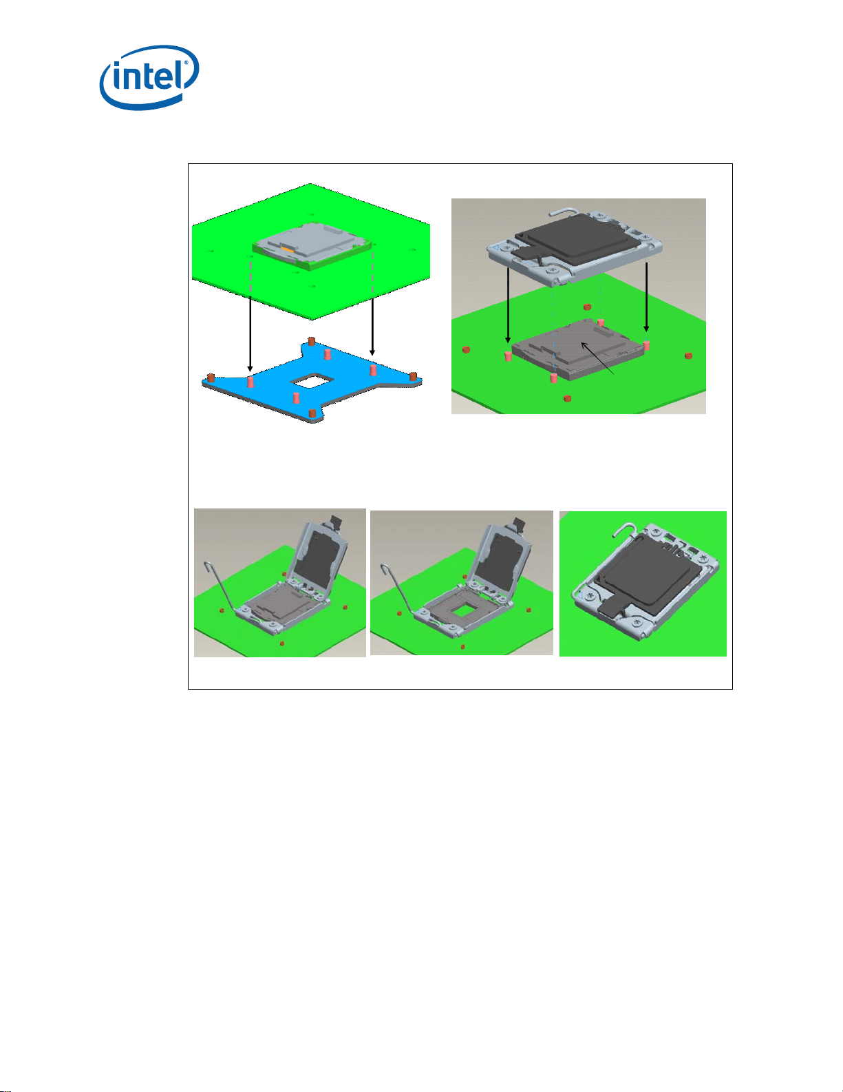
3.2 Assembly of ILM to a Motherboard
The ILM design allows a bottoms up assembly of the components to the board. In step
1 (see Figure 3-3), the back plate is placed in a fixture. Holes in the motherboard
provide alignment to the threaded studs.
In step 2, the ILM assembly is placed over the socket and threaded studs. The Intel
Reference Design ILM cover is not designed to nest over the Pick and Place cover. This
feature helps prevent reinstallation of the Pick and Place cover, a step that can lead to
socket bent contacts.
To prevent the ILM cover from popping off during ILM assembly, the load plate can be
unlatched from the load lever when the fasteners are torqued as shown is Step 3. Using
a T20 Torx* driver, fasten the ILM assembly to the back plate with the four captive
fasteners. Torque to 9 ± 1 inch-pounds.
The Pick and Place cover can then be removed as shown in Step 4, and the load plate
can then closed and latched as shown in Step5.
The length of the threaded studs accommodate board thicknesses from
0.062” to 0.100”.
Intel® Xeon® Processor E5-2400 Product Family 25
Thermal/Mechanical Design Guide
Page 26
.
ILM co ver
Step 1: With socket body reflowed
on board, and back plate in fixture,
align board holes to back plate studs.
Step 2: With back plate against
bottom of board, align ILM assembly
to back plate studs.
ILM cover
Pick and
Place Cover
Step 3
Step 4 Step 5
Figure 3-3. ILM Assembly
Independent Loading Mechanism (ILM) and Back Plate
26 Intel® Xeon® Processor E5-2400 Product Family
Thermal/Mechanical Design Guide
Page 27
Independent Loading Mechanism (ILM) and Back Plate
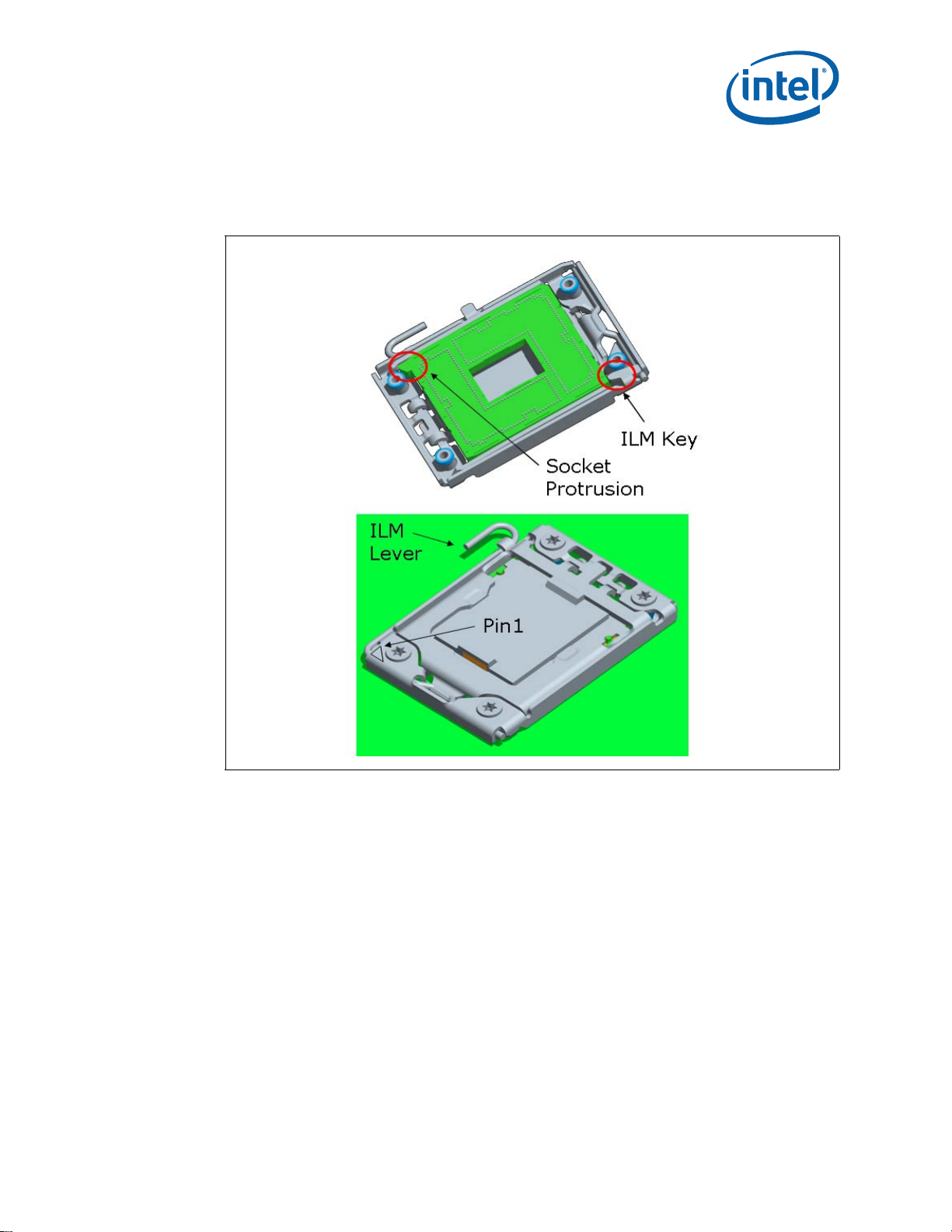
As indicated in Figure 3-4, socket protrusion and ILM key features prevent 180-degree
rotation of ILM assembly with respect to the socket. The result is a specific Pin 1
orientation with respect to the ILM lever.
Figure 3-4. Pin1 and ILM Lever
3.3 ILM Cover
As indicated in Table A-4, ILM covers are available as discrete components and preassembled to the ILM load plate.
The ILM cover will interfere with a processor and pop off if the ILM is closed with a
processor in the socket.
The ILM cover is designed to be interchangeable between different suppliers validated
by Intel. Performance of the pop off feature may decline if the ILM cover supplier is
different than the ILM supplier. The ILM cover can be removed manually if the pop off
feature is not desirable, or not functional.
The ILM cover has UL94 V-0 flammability rating.
The ILM cover durability requirement is 20 cycles (1 cycle = install and remove).
§
Intel® Xeon® Processor E5-2400 Product Family 27
Thermal/Mechanical Design Guide
Page 28

Independent Loading Mechanism (ILM) and Back Plate
28 Intel® Xeon® Processor E5-2400 Product Family
Thermal/Mechanical Design Guide
Page 29
LGA1356 Socket, ILM and Back Plate Electrical, Mechanical, and Environmental Specifications
4 LGA1356 Socket, ILM and Back
Plate Electrical, Mechanical,
and Environmental
Specifications
This chapter describes the electrical, mechanical, and environmental specifications for
the LGA1356 socket, Independent Loading Mechanism and Back Plate.
4.1 Component Mass
Table 4-1. Component Mass
Component Mass
Socket Body, Contacts and PnP Cover 15 gm
ILM Assembly 43 gm
Back Plate 100 gm
4.2 Package/Socket Stackup Height
Table 4-2 provides the stackup height of a processor in the 1356-land LGA package and
LGA1356 socket with the ILM closed and the processor fully seated in the socket.
Table 4-2. 1356-land Package and LGA1356 Socket Stackup Height
Integrated Stackup Height (mm)
From Top of Board to Top of IHS
Notes:
1. This data is provided for information only, and is derived from: (a) the height of the socket seating plane
above the motherboard after reflow, given in Appendix C, (b) the height of the packag e, fr om the pac kage
seating plane to the top of the IHS, and accounting for its nominal variation and tolerances that are given
in the corresponding processor EDS and expected values for the follow-on processor.
2. This value is a RSS calculation.
7.753 ± 0.262 mm
4.3 Socket Maximum Temperature
The power dissipated within the socket is a function of the current at the pin level and
the effective pin resistance. To ensure socket long term reliability, Intel defines socket
maximum temperature using a via on the underside of the motherboard. Exceeding the
temperature guidance may result in socket body deformation, or increases in thermal
and electrical resistance which can cause a thermal runaway and eventual electrical
failure. The guidance for socket maximum temperature is listed below:
• Via temperature under socket < 96 °C
Intel® Xeon® Processor E5-2400 Product Family 29
Thermal/Mechanical Design Guide
Page 30
LGA1356 Socket, ILM and Back Plate Electrical, Mechanical, and Environmental Specifications
4.4 Loading Specifications
The socket will be tested against the conditions listed in the LGA1366 Socket Validation
Reports, and LGA1356 Addendum, with heatsink, ILM and back plate attached, under
the loading conditions outlined in this chapter.
Table 4-3 provides load specifications for the LGA1356 socket with the ILM and back
plate installed. The maximum limits should not be exceeded during heatsink assembly,
shipping conditions, or standard use condition. Exceeding these limits during test may
result in component failure. The socket body should not be used as a mechanical
reference or load-bearing surface for thermal solutions.
Table 4-3. Socket and ILM Mechanical Specifications
Parameter Min Max Notes
Static compressive load from ILM to processor
IHS
Thermal Solution Static Compressive Load 0 N [0 lbf] 266 N [60 lbf] 1, 2, 3
Total Static Compressive Load
(ILM plus Heatsink)
Dynamic Compressive Load
(with heatsink installed)
Target Pick and Place Cover allowable removal
force
Load Lever actuation force N/A 38.3 N [8.6 lbf] in the
445 N [100 lbf] 623 N [140 lbf] 3, 4
445 N (100 lbf) 890 N (200 lbf) 3, 4
N/A 890 N [200 lbf] 1, 3, 5, 6
N/A 4.45 - 6.68 N [1.0 -
1.5 lbf]
vertical direction
10.2 N [2.3 lbf] in the
lateral direction.
Notes:
1. These specifications apply to uniform compressive loading in a direction perpendicular to the IHS top
surface.
2. This is the minimum and maximum static force that can be applied by the heatsink and it’s retention
solution to maintain the heatsink to IHS interface. This does not imply the Intel reference TIM is validated
to these limits. TIM load range is documented in Section 5.2 for the Intel Reference Design.
3. Loading limits are for the LGA1356 socket.
4. This minimum limit defines th e compressi ve forc e required to electrically seat the processor onto the sock et
contacts.
5. Dynamic loading is defined as an 11 ms duration average load superimposed on the static load
requirement.
6. T est condition used a heatsink mass of 550 gm [1.21 lb] with 50 g acceler ation measured at heatsi nk mass.
The dynamic portion of this specification in the product application can have flexibility in specific values, but
the ultimate product of mass times acceleration should not exceed this dynamic load.
4.5 Electrical Requirements
LGA1356 socket electrical requirements are measured from the socket-seating plane of
the processor to the component side of the socket PCB to which it is attached. All
specifications are maximum values (unless otherwise stated) for a single socket
contact, but includes effects of adjacent contacts where indicated.
30 Intel® Xeon® Processor E5-2400 Product Family
Thermal/Mechanical Design Guide
Page 31

LGA1356 Socket, ILM and Back Plate Electrical, Mechanical, and Environmental Specifications
Table 4-4. Electrical Requirements for LGA1356 Socket
Parameter Value Comment
The inductance calculated for two contacts,
Mated loop inductance, Loop <3.9 nH
Maximum mutual capacitance, C. <1 pF The capacitance between two contacts
Socket Average Contact R esistance
(EOL)
Max Individual Contact Resistance
(EOL)
Bulk Resistance Increase ≤
Dielectric Withstand Voltage 360 Volts RMS
Insulation Resistance 800 MΩ
15.2 mΩ
100 mΩ
≤
3 mΩ
considering one forward conductor an d one return
conductor. These values must be satisfied at the
worst-case height of the socket.
The socket average contact resistance target is
derived from average of every chain contact
resistance for each part used in testing, with a
chain contact resistance defined as the resistance
of each chain minus resistance of shorting bars
divided by number of lands in the daisy chain.
The specification listed is at room temperature
and has to be satisfied at all time.
Socket Contact Resistance: The resistance of
the socket contact, solderball, and interface
resistance to the interposer land.
The specification listed is at room temperature
and has to be satisfied at all time.
Socket Contact Resistance: The resistance of
the socket contact, solderball, and interface
resistance to the interposer land; gaps included.
The bulk resistance increase per contact from
24 °C to 107 °C
4.6 Environmental Requirements
The reliability targets in this chapter are based on the expected field use environment
for these products. The test sequence for the LGA1356 socket was developed using the
knowledge-based reliability evaluation methodology, which is acceleration factor
dependent. A simplified process flow of this methodology can be seen in Figure 4-1.
Since the LGA1356 socket is very similar to the LGA1366 socket, the LGA1356 socket is
expected to perform similarly and full validation for the LGA1356 socket is avoided.
Intel® Xeon® Processor E5-2400 Product Family 31
Thermal/Mechanical Design Guide
Page 32

LGA1356 Socket, ILM and Back Plate Electrical, Mechanical, and Environmental Specifications
Establish the
market/expected use
environment for the
technology
Develop Speculative
stress conditions based on
historical data, content
experts, and literature
search
Perform stressing to
validate accelerated
stressing assumptions and
determine acceleration
factors
Freeze stressing
requirements and perform
additional data turns
Figure 4-1. Flow Chart of Knowledge-Based Reliability Evaluation Methodology
A detailed description of this methodology can be found at:
ftp://download.intel.com/technology/itj/q32000/pdf/reliability.pdf.
§
32 Intel® Xeon® Processor E5-2400 Product Family
Thermal/Mechanical Design Guide
Page 33

Thermal Solutions
Notes:
5 Thermal Solutions
This section describes a 1U reference heatsink and thermal design guidelines for the
Intel® Xeon® Processor E5-2400 Product Family.
5.1 Boundary Conditions
Table 5-1 provides values for boundary conditions and performance targets used to
generate processor thermal specifications and to provide guidance for heatsink design.
Table 5-1. Values Used to Generate Processor Thermal Specifications
Parameter Value
Altitude, system
ambient temp
TDP
1
Ψ
CA
2
T
LA
3
Airflow
System height
(form factor)
Heatsink
volumetric
Heatsink
technology
5
7
Sea level, 35
50W (4-
core)
o
C/W 0.296oC/W 0.296oC/W 0.315oC/W
0.312
60W 70W 80W (4-core) 95W
o
49
C48.1
9.7 CFM @ 0.23” dP
1U (EEB)
90 x 90 x 25.5 mm (1U/SSI blade)
Cu base, Al fins
4
o
C
0.296
0.298
o
C/W
(8-core),
o
C/W
(6-core)
6
80W (2-core,
1 socket)
o
0.285
C/W
o
C
13 CFM @
0.28” dP
1U
(non-specific,
1-socket)
1. Max target (mean + 3 sigma + offset) for thermal characterization parameter (Section 5.4.1).
2. Local ambient temperature of the air entering the heatsink.
3. Airflow through the heatsink fins with zero bypa ss. Max target for pressure drop (dP) meas ured in inches H2O.
4. Reference system configuration. Processor is downstream from me mory in EEB (Entry-Level Electronics Bay).
Values above do not apply to LR-DIMM in an Intel Reference Design. Ducting is utilized to direct airflow.
5. Dimensions of heatsink do not include socket or processor.
6. Heatsink height + socket/processor height (Table 4-2) complies with TEB 1U Rack Height Constraints
(36 mm) in EEB Specification 2011, and with Maximum Component Height (33.5 mm) in SSI Compute Blade
Specification, both at http://www.ssiforum.org.
7. Passive heatsinks. PCM45F thermal interface material.
Table 5-2 provides approximate boundary conditions and approximate performance
expectations in Compact Electronics Bay. These values are not used to generate
processor thermal specifications, but may provide guidance for heatsink design.
Table 5-2. Performance Expectations in Compact Electronics Bay (CEB)
Parameter Value
Altitude, system
ambient temp
TDP 50W 60W 70W 80W (4-core) 95W
1
T
LA
Intel® Xeon® Processor E5-2400 Product Family 33
Thermal/Mechanical Design Guide
43.7oC 45.6oC 46.8oC 48.1oC
Sea level, 35
o
C
o
C (8-core),
50.0
o
C (6-core)
46.6
Page 34

Notes:
Table 5-2. Performance Expectations in Compact Electronics Bay (CEB)
Parameter Value
2
Ψ
CA
3
Airflow
System height
(form factor)
Heatsink
volumetric
Heatsink
technology
1. Local ambient temperature of the air entering the heatsink.
2. Max target (mean + 3 sigma + offset) for thermal characterization parameter (Section 5.4.1).
3. Airflow through the heatsink fins with zero bypass. Max target for pressure drop (dP) measured in
4. Reference system configuration. Processor is downstream from processor in CEB (Compact
5. Dimensions of heatsink do not include socket or processor.
6. Heatsink height + socket/processor height (Table 4-2) complies with TEB 1U Rack Height
7. Passive heatsinks. PCM45F thermal interface material.
5
inches H
Electronics Bay). With the values above, the 25.5mm tall heatsink can meet the processor thermal
specifications in Intel's Reference Design 10.5x12 inches CEB board. However, these CEB values are
not used to generate processor thermal specifications. Ducting is utilized to direct airflow.
Constraints (36 mm) in EEB Specification 2011, and with Maximum Component Height (33.5 mm)
in SSI Compute Blade Specification, both at http://www.ssiforum.org.
0.273oC/W 0.265oC/W 0.264oC/W 0.278oC/W
13 CFM @ 0.32” dP
4
1U (CEB)
90 x 90 x 25.5 mm (1U/SSI blade)
7
O.
2
Cu base, Al fins
0.265
0.269
6
Thermal Solutions
o
C/W (8-core),
o
C/W (6-core)
Table 5-1 and Table 5-2 spe c ify ΨCA and pressure drop targets for specific airflows. To
determine ΨCA and pressure drop targets for other airflows, use Best-fit equations in
Figure 5-1. Heatsink detailed drawings are in Appendix A.
Figure 5-1. Best-fit Equations
34 Intel® Xeon® Processor E5-2400 Product Family
Thermal/Mechanical Design Guide
Page 35

Thermal Solutions
5.2 Assembly
Figure 5-2. 1U Reference Heatsink Assembly
The assembly process for the 1U reference heatsink begins with application of
Honeywell PCM45F thermal interface material to improve conduction from the IHS.
Tape and roll format is recommended. Pad size is 35 x 35 mm, thickness is 0.25 mm.
Next, position the heatsink such that the heatsink fins are parallel to system airflow.
While lowering the heatsink onto the IHS, align the four captive screws of the heatsink
to the four threaded nuts of the back plate.
Using a #2 Phillips driver, torque the four captive screws to 8 inch-pounds. Fastener
sequencing, in other words starting the threads on all four screws before torquing, may
mitigate against cross threading.
This assembly process is designed to produce a static load of 39 - 51 lbf, for 0.062" -
0.100" board thickness respectively. Honeywell PCM45F is expected to meet the
performance targets in Table 5-1 and Table 5-2 from 30 - 60 lbf. From Table 4-3, the
Heatsink Static Compressive Load of 0 - 60 lbf allows for designs that vary from the 1U
reference heatsink. Example: A customer’s unique heatsink with very little static load
(as little as 0 lbf) is acceptable from a socket loading perspective as long as the
thermal specifications are met.
Compliance to Board Keepout Zones in Appendix A is assumed for this
assembly process.
Intel® Xeon® Processor E5-2400 Product Family 35
Thermal/Mechanical Design Guide
Page 36

5.2.1 Thermal Interface Material (TIM)
TIM should be verified to be within its recommended shelf life before use.
Surfaces should be free of foreign materials prior to application of TIM.
Use isopropyl alcohol and a lint free cloth to remove old TIM before applying new TIM.
5.3 Structural Considerations
Target mass of heatsinks should not exceed 500 gm.
From Table 4-3, the Dynamic Compressive Load of 200 lbf max allows for designs that
exceed 500 gm as long as the mathematical product does not exceed 200 lbf. Example:
A heatsink of 2-lb mass (908 gm) x 50 g (acceleration) x 2.0 Dynamic Amplification
Factor = 200 lbf. The Total Static Compressive Load (Table 4-3) should also be
considered in dynamic assessments.
Direct contact between back plate and chassis pan will help minimize board deflection
during shock. Placement of board-to-chassis mounting holes also impacts board
deflection and resultant socket solder ball stress. Customers need to assess shock for
their designs as their heatsink retention (back plate), heatsink mass and chassis
mounting holes may vary.
Thermal Solutions
5.4 Thermal Design
5.4.1 Thermal Characterization Parameter
The case-to-local ambient Thermal Characterization Parameter (ΨCA) is defined by:
Equation 5-1.ΨCA = (T
Where:
T
CASE
T
LA
TDP = TDP (W) assumes all power dissipates through the integrated heat
Equation 5-2.Ψ
= ΨCS + ΨSA
CA
Where:
Ψ
CS
Ψ
SA
Figure 5-3 illustrates the thermal characterization parameters.
CASE
- TLA) /
TDP
= Processor case temperature (°C). For T
appropriate External Design Specification (EDS).
= Local ambient temperature in chassis at processor (°C).
spreader. This inexact assumption is convenient for heatsink design.
TTVs are often used to dissipate TDP. Correction offsets account for
differences in temperature distribution between processor and TTV.
= Thermal characterization parameter of the TIM (°C/W) is dependent
on the thermal conductivity and thickness of the TIM.
= Thermal characterization parameter from heatsink-to-local ambient
(°C/W) is dependent on the thermal conductivity and geometry of the
heatsink and dependent on the air velocity through the heatsink fins.
specification see the
CASE
36 Intel® Xeon® Processor E5-2400 Product Family
Thermal/Mechanical Design Guide
Page 37

Thermal Solutions
Figure 5-3. Processor Thermal Characterization Parameter Relationships
5.5 Fan Speed Control
5.5.1 Fundamentals
In server platforms, processors often share airflow provided by system fans with other
system components such as chipset, memory and hard drives. As such, the thermal
control features in chipset, memory and other components not covered in this
document, should influence system fan speed control to reduce fan power consumption
and help systems meet acoustic targets.
The addition of thermal sensors placed in the system (for example, on front panel or
motherboard) to augment internal device sensors (for example, in processor, chipset
and memory) will improve the ability to implement need-based fan speed control. The
placement of system sensors in cooling zones, where each zone has dedicated fan(s),
can improve the ability to tune fan speed control for optimal performance and/or
acoustics.
System events such as fan or power supply failure, device events such as TCC
Activation or THERMTRIP, and maintenance events such as hot swap time allowance,
need to be comprehended to implement appropriate fan speed control to prevent
undesirable performance or loss of data. For more information on device events and
features see the appropriate processor Datasheet.
Tcontrol and its upper and lower limits defined by hysteresis, can be used to avoid fan
speed oscillation and undesirable noise variations.
5.6 Thermal Features
More information regarding processor thermal features is contained in the appropriate
datasheet.
Intel® Xeon® Processor E5-2400 Product Family 37
Thermal/Mechanical Design Guide
Page 38

Thermal Solutions
5.6.1 T
CONTROL
and DTS Relationship
Improved acoustics and lower fan power can be achieved by understanding the
Table 5-3. T
T
CONTROL
CONTROL
DTS ≤ T
DTS > T
and DTS relationship, and implementing fan speed control accordingly.
and DTS Relationship
Condition Fan Speed Control
CONTROL
CONTROL
Adjust fan speed to maintain DTS ≤ T
Adjust fan speed to keep T
EDS, or adjust fan speed to keep DTS at or below the DTS based thermal profile in
the EDS.
CASE
CONTROL
at or below the T
5.6.1.1 Sign Convention and Temperature Filtering
Digital Thermal Sensor (DTS) and Tcontrol are relative die temperatures offset below
the Thermal Control Circuit (TCC) activation temperature. As such, negative sign
conventions are understood. While DTS and Tcontrol are available over PECI and MSR,
use of these values in fan speed control algorithms requires close attention to sign
convention. See Table 5-4 for the sign convention of various sources.
Table 5-4. Sign Convention
MSR (BWG) PECI (EDS)
DTS
T
CONTROL
(+) using
PACKAGE_THERM_STA TUS (22:16,
Digital Readout)
(+) using TEMPERATURE_TARGET
(15:8, Temperature Control Offset)
(-) using GetTemp()
(+) using T emperature T arget R ead
from RdPkgConfig()
.
based thermal profile in the
CASE
Where a positive (+) sign convention is shown in Table 5-4, no sign bit is actually
assigned, so writers of firmware code may mistakenly assign a positive sign convention
in firmware equations. As appropriate, a negative sign should be introduced.
Where a negative (-) sign convention is shown in Table 5-4, a sign bit is assigned, so
firmware code will read a negative sign convention in firmware equations, as desired.
DTS obtained thru MSR (PACKAGE_THERM_STATUS) is an instantaneous value. As
such, temperature readings over short time intervals may vary considerably using this
MSR. For this reason, DTS obtained thru PECI GetTemp() may be preferred since
temperature filtering will provide the thermal trend.
5.6.1.2 Tcontrol Relief
Factory configured T
Letter or may be extracted by issuing a Mailbox or an RDMSR instruction. See the
appropriate External Design Specification (EDS) for more information.
Due to increased thermal headroom based on thermal characterization on the latest
processors, customers have the option to reduce T
factory configured values.
In some situations, use of T
acoustics. There are no plans to change Intel's specification or the factory configured
T
CONTROL
values on individual processors.
CONTROL
values are available in the appropriate Dear Customer
to values lower than the
CONTROL
CONTROL
Relief can reduce average fan power and improve
38 Intel® Xeon® Processor E5-2400 Product Family
Thermal/Mechanical Design Guide
Page 39

Thermal Solutions
Table 5-5. T
To implement this relief, customers must re-write code to set T
CONTROL
to the reduced
values provided in the table below. Implementation is optional. Alternately, the factory
configured T
CONTROL
configured and Relief. Regardless of T
values can still be used, or some value between factory
CONTROL
values used, BIOS needs to identify the
processor type.
CONTROL
Relief for Intel® Xeon® Processor E5-2400 Product Family
TDP, # Core T
95W 8C -6 2.30 GHz or lower -10
95W 6C -6 2.40 GHz or lower -10
70W 8C -6 1.80 GHz or lower -10
60W 6C -6 2.00 GHz or lower -10
80W 4C -6 2.20 GHz or lower -10
80W 2C, 1S -6 2.80 GHz or lower -10
CONTROL
Relief Max Core Frequency Factory Configured
In some cases, use of Tcontrol Relief as the trigger point for fan speed control may
result in excessive TCC activation. To avoid this, the adjusted trigger point for fan
speed control (FSC) is defined as:
Tcontrol_FSC = - T
CONTROL
+ Tcontrol_offset
Tcontrol_offset must be chosen such that Tcontrol_FSC < Tcontrol Relief. As such,
Tcontrol_FSC is an earlier trigger point for fan speed control, as compared to Tcontrol
Relief, and can be interpreted as overcooling. When overcooling to Tcontrol_FSC,
margin as defined in Section 5.8.3 and Section 5.8.6 can be ignored. As compared to
cooling to Tcontrol Relief, overcooling to Tcontrol_FSC:
• May increase frequency benefit from Intel TBT as defined in Section 5.6.3.
• Will increase acoustics
• May result in lower wall power
Customers must characterize a Tcontrol_offset value for their system to meet their
goals for frequency, acoustics and wall power.
5.6.2 Short Duration TCC Activation and Catastrophic Thermal Management for Intel® Xeon® Processor E5-2400 Product Family
Systems designed to meet thermal capacity may encounter short durations of
throttling, also known as TCC activation, especially when running non-steady processor
stress applications. This is acceptable and is functionally within the intended
temperature control parameters of the processor. Such short duration TCC activ ation is
not expected to provide noticeable reductions in application performance, and is
typically within the normal range of processor to processor performance variation.
Normal amounts of TCC activation occur at PECI values less than -0.25. Such
occurrences may cause utilities or operating systems to issue error log.
PECI = -0.25 indicates a catastrophic thermal failure condition in all studies conducted.
As such, to help prevent loss of data, a soft shutdown can be initiated at PECI = -0.25.
Since customer designs, boundary conditions, and failure scenarios differ, this guidance
should be tested in the customer's system to prevent loss of data during shutdown.
PECI command GetTemp() can be used to obtain non-integer PECI values.
Intel® Xeon® Processor E5-2400 Product Family 39
Thermal/Mechanical Design Guide
Page 40

5.6.3 Intel® Turbo Boost Technology
Intel® Turbo Boost Technology (Intel® TBT), available on certain processor SKUs,
opportunistically , and automatically, allows the processor to run faster than the marked
frequency if the part is operating below its power, temperature and current limits.
Thermal Solutions
Heatsink performance (lower Ψ
factors that can impact the amount of Intel TBT frequency benefit. Intel TBT
performance is also constrained by ICC, and VCC limits.
Increased IMON accuracy may provide more Intel TBT benefit on TDP limited
applications, as compared to lower Ψ
these workloads.
With Intel TBT enabled, the processor may run more consistently at higher power levels
(but still within TDP), and be more likely to operate above T
when Intel TBT is disabled. This may result in higher acoustics.
5.7 Thermal Guidance
5.7.1 Thermal Excursion
Under fan failure or other anomalous thermal excursions, Tcase may exceed the
thermal profile for a duration totaling less than 360 hours per year without affecting
long term reliability (life) of the processor. For more typical thermal excursions,
Thermal Monitor is expected to control the processor power level as long as conditions
do not allow the Tcase to exceed the temperature at which Thermal Control Circuit
(TCC) activation initially occurred. Under more severe anomalous thermal excursions
when the processor temperature cannot be controlled at or below this Tcase level by
TCC activation, then data integrity is not assured. At some higher threshold,
THERMTRIP_N will enable a shut down in an attempt to prevent permanent damage to
the processor. Thermal Test Vehicle (TTV) may be used to check anomalous thermal
excursion compliance by ensuring that the processor Tcase value, as measured on the
TTV, does not exceed Tcase_max at the anomalous power level for the environmental
condition of interest. This anomalous power level is equal to 75% of the Thermal
Design Power (TDP) limit.
as described in Section 5.4.1) is one of several
CA
, as temperature is not typically the limiter for
CA
CONTROL
, as compared to
This guidance can be applied to 95W, 80W, 70W, 60W Standard or Basic SKUs in the
Intel® Xeon® Processor E5-2400 Product Family.
5.7.2 Absolute Processor Temperature
Intel does not test any third party software that reports absolute processor
temperature. As such, Intel cannot recommend the use of software that claims this
capability. Since there is part-to-part variation in the TCC (thermal control circuit)
activation temperature, use of software that reports absolute temperature can be
misleading.
See the appropriate Datasheet for details regarding use of TEMPERATURE_TARGET
register to determine the minimum absolute temperature at which the TCC will be
activated and PROCHOT# will be asserted.
40 Intel® Xeon® Processor E5-2400 Product Family
Thermal/Mechanical Design Guide
Page 41

Thermal Solutions
5.8 DTS Based Thermal Specification
5.8.1 Compliance to Tcase Based Thermal Profile
Processor heatsink design must still comply with the Tcase based thermal profile
provided in the Intel® Xeon® Processor E5-2400 Product Family Datasheet - Volume
One. Heatsink design compliance can be determined with thermocouple and TTV as
with previous processors.
The heat sink is sized to comply with the Tcase based thermal profile. Customers have
an option to either follow processor based Tcase spec or follow the DTS based thermal
specification. In some situations, implementation of DTS based thermal specification
can reduce average fan power and improve acoustics as compared to the Tcase based
thermal profile.
When all cores are active, a properly sized heatsink will be able to meet the DTS based
thermal specification. When all cores are not active or when Intel Turbo Boost
Technology is active, attempting to comply with the DTS based thermal specification
may drive system fans to maximum speed. In such situations, the T
will be below the T
5.8.2 Considerations for Follow-on Processor
based thermal profile by design.
CASE
temperature
CASE
The follow-on processor in the platform will have new capabilities as compared to the
Intel® Xeon® Processor E5-2400 Product Family. For example, the follow-on processor
has a new Package Configuration Space (PCS) command to read margin (M) from the
processor: RdPkgConfig(), Index 10. For the Intel® Xeon® Processor E5-2400 Product
Family, margin (M) must be calculated in firmware.
In the following sections, implementation details specified for the Intel® Xeon®
Processor E5-2400 Product Family can also be used for the follow-on processor.
For more information regarding the differences between the follow-on processor and
the Intel® Xeon® Processor E5-2400 Product Family see Platform Digital Thermal
Sensor (DTS) Based Thermal Specifications and Overview.
5.8.3 DTS Based Thermal Profile, Tcontrol and Margin for the Intel® Xeon® Processor E5-2400 Product Family
The calculation of the DTS based thermal specification is based on both Tcontrol and
the DTS Based Thermal Profile (T
T
= min[TLA + Ψpa * P * F, TEMPERATURE_TARGET [23:16] – Tcc_Offset]
DTS
Where T
+ Ψpa are the intercept and slope terms from the T
LA
appropriate External Design Specification (EDS). To implement the DTS based thermal
specification, these equations must be programmed in firmware. Since the equations
differ with processor SKU, SKUs can be identified by TDP, Core Count and a profile
identifier (CSR bits). For associated commands, see Platform Digital Thermal Sensor
(DTS) Based Thermal Specifications and Overview.
DTS
):
equations in the
DTS
Power (P) is calculated in Section 5.8.4. As power dynamically changes, the
specification also changes, so power and T
calculations are recommended every 1
DTS
second.
Correction factor (F) compensates for the error in power monitoring. The current
estimate for F is 0.95.
Intel® Xeon® Processor E5-2400 Product Family 41
Thermal/Mechanical Design Guide
Page 42

Thermal Solutions
The Tcontrol portion of the DTS based thermal specification is a one time calculation:
T
control_spec
= TEMPERATURE_TARGET [23:16] - Tcontrol + Tcontrol_offset
Tcontrol is defined in Section 5.6.1.1. Tcontrol_offset is defined in Section 5.6.1.2.
The final DTS based thermal specification is the maximum of both:
T
DTS_max
= max[T
control_spec
, T
DTS
]
The margin (M) between the actual die temperature and the DTS based thermal
specification is used in the fan speed control algorithm. When M < 0, increase fan
speed. When M ≥ 0, fan speed may decrease.
M = T
DTS_max
- Tsensor
OR
M = T
DTS_ave
– Tsensor
Tsensor represents the absolute temperature of the processor as power changes:
Tsensor = TEMPERATURE_TARGET [23:16] + DTS
T
DTS_ave
is defined in Section 5.8.5.
TEMPERATURE_TARGET [23:16], the temperature at which the processor thermal
control circuit activates, is a one time PECI readout: RdPkgConfig(), Temperature
Target Read, 23:16.
DTS, the relative temperature from thermal control circuit activation, is negative by
definition, and changes instantaneously. DTS command info is given in Section 5.6.1.1.
5.8.4 Power Calculation for the Intel® Xeon® Processor E52400 Product Family
To imple ment DTS based thermal specification, average power over time must be
calculated:
P = (E2 - E1) / (t2 - t1)
Where:
t1 = time stamp 1
t2 = time stamp 2
E1 = Energy readout at time t1
E2 = Energy readout at time t2
The recommended time interval between energy readings is 1 second. This helps
ensure the power calculation is accurate by making the error between time stamps
small as compared to the duration between time stamps.
For details regarding energy readings, see Platform Digital Thermal Sensor (DTS)
Based Thermal Specifications and Overview.
5.8.5 Averaging the DTS Based Thermal Specification for the Intel® Xeon® Processor E5-2400 Product Family
Averaging the DTS Based Thermal Specification helps keep the rate of change of the
temperature specification on the same scale as the actual processor temperature, and
helps avoid rapid changes in fan speed when power changes rapidly.
42 Intel® Xeon® Processor E5-2400 Product Family
Thermal/Mechanical Design Guide
Page 43

Thermal Solutions
An exponential average of the specification can be calculated using a two time constant
model:
= αf x DT x T
T
DTS_f
T
DTS_s
T
DTS_ave
= αs x DT x T
= C x T
DTS_max
DTS_f
Where:
T
DTS_max
T
DTS_f
T
DTS_ave
and αs are the time constant coefficients
α
f
is the instantaneous spec
and T
are the fast and slow time averages
DTS_s
is the final two time constant average specification
C is a scale factor
DT is the scan rate and is recommended to be approximately 1 second
Table 5-6 below shows the coefficients recommended for averaging. These values may
change per processor SKU. Customers should tune these coefficients based on their
thermal solutions.
Table 5-6. Averaging Coefficients
+ T
DTS_max
+ T
+ (1-C) x T
DTS_f_previous
DTS_s_previous
DTS_s
x (1- αf x DT)
x (1- αs x DT)
Heatsink
Performance
Low 1.0 0.04 0.30 based on typical processor
Medium 1.0 0.07 0.30 based on typical processor
High 1.0 0.10 0.40 based on typical processor
α
(1/s) αs (1/s) C Comment
f
5.8.6 Capabilities for the Follow-on Processor
For the follow-on processor, the intercept and slope terms from the T
(TLA, Ψpa), as defined in Section 5.8.3, are stored in the processor. This allows margin
(M) to be reported by the processor. The PECI command for margin (M) will be
RdPkgConfig(), Index 10.
M < 0; gap to spec, fan speed must increase
M ≥ 0; margin to spec, fan speed may decrease
Use of RdPkgConfig(), Index 10 with the Intel® Xeon® Processor E5-2400 Product
Family will return an illegal command.
For the follow-on processor, coefficients (α
(F) will be factory configured.
, αs), scale factor (C) and correction factor
f
§
equations
DTS
Intel® Xeon® Processor E5-2400 Product Family 43
Thermal/Mechanical Design Guide
Page 44

Thermal Solutions
44 Intel® Xeon® Processor E5-2400 Product Family
Thermal/Mechanical Design Guide
Page 45

Quality and Reliability Requirements
6 Quality and Reliability
Requirements
6.1 Test Conditions
Test Conditions, Qualification and Visual Criteria vary by customer.
Socket Test Conditions are provided in the LGA1366 Socket Validation Reports, and
LGA1356 Addendum and are available from socket suppliers listed in Appendix A.
6.2 Intel Reference Component Validation
Intel tests reference components both individually and as an assembly on mechanical
test boards, and assesses performance to the envelopes specified in previous sections
by varying boundary conditions.
While component validation shows that a reference design is tenable for a limited range
of conditions, customers need to assess their specific boundary conditions and perform
reliability testing based on their use conditions.
Intel reference components are also used in board functional tests to assess
performance for specific conditions.
6.2.1 Board Functional Test Sequence
Each test sequence should start with components (baseboard, heatsink assembly, and
so on) that have not been previously submitted to any reliability testing.
The test sequence should always start with a visual inspection after assembly and
BIOS/Processor/memory test. The stress test should be then followed by a visual
inspection and then BIOS/Processor/memory test.
6.2.2 Post-Test Pass Criteria
The post-test pass criteria are:
1. No significant physical damage to the heatsink and retention hardware.
2. Heatsink remains seated and its bottom remains mated flat against the IHS
surface. No visible gap between the heatsink base and processor IHS. No visible tilt
of the heatsink with respect to the retention hardware.
3. No signs of physical damage on baseboard surface due to impact of heatsink.
4. No visible physical damage to the processor package.
5. Successful BIOS/Processor/memory test.
6. Thermal compliance testing to demonstrate that the case temperature specification
can be met.
Intel® Xeon® Processor E5-2400 Product Family 45
Thermal/Mechanical Design Guide
Page 46

Quality and Reliability Requirements
6.2.3 Recommended BIOS/Processor/Memory Test Procedures
This test is to ensure proper operation of the product before and after environmental
stresses, with the thermal mechanical enabling components assembled. The test shall
be conducted on a fully operational baseboard that has not been exposed to any
battery of tests prior to the test being considered.
The testing setup should include the following components, properly assembled and/or
connected:
• Appropriate system baseboard.
• Processor and memory.
• All enabling components, including socket and thermal solution parts.
The pass criterion is that the system under test shall successfully complete the
checking of BIOS, basic processor functions and memory, without any errors.
6.3 Material and Recycling Requirements
Material shall be resistant to fungal growth. Examples of non-resistant materials
include cellulose materials, animal and vegetable based adhesives, grease, oils, and
many hydrocarbons. Synthetic materials such as PVC formulations, certain
polyurethane compositions (for example, polyester and some polyethers), plastics
which contain organic fillers of laminating materials, paints, and varnishes also are
susceptible to fungal growth. If materials are not fungal growth resistant, then MILSTD-810E, Method 508.4 must be performed to determine material performance.
Any plastic component exceeding 25 gm should be recyclable per the European Blue
Angel recycling standards.
The following definitions apply to the use of the terms lead-free, Pb-free, and RoHS
compliant.
Lead-free and Pb-free: Lead has not been intentionally added, but lead may still
exist as an impurity below 1000 ppm.
RoHS compliant: Lead and other materials banned in RoHS Directive are either
(1) below all applicable substance thresholds as proposed by the EU or (2) an
approved/pending exemption applies.
Note: RoHS implementation details are not fully defined and may change.
§
46 Intel® Xeon® Processor E5-2400 Product Family
Thermal/Mechanical Design Guide
Page 47

Component Suppliers
A Component Suppliers
Various suppliers have developed support components for processors in the Intel®
Xeon® Processor E5-2400 Product Family-based platform. These suppliers and
components are listed as a convenience to customers. Intel does not guarantee
quality, reliability, functionality or compatibility of these components. The supplier list
and/or the components may be subject to change without notice. Customers are
responsible for the thermal, mechanical, and environmental verification of the
components with the supplier.
A.1 Intel Enabled Supplier Information
Performance targets for heatsinks are described in Section 5.1. Mechanical drawings
are provided in Appendix A. Mechanical models are listed in Table 1-1. Heatsinks
assemble to server back plate Table A-4.
A.1.1 Intel Reference Thermal Solution
Customers can purchase the Intel reference thermal solutions from the suppliers listed
in Table A-1.
Table A-1. Suppliers for the Intel Reference Thermal Solution
Assembly Component Description Supplier PN Supplier Contact Info
Assembly, Heat
Sink, Intel Xeon
processor E52400 product
family, 1U
1U URS Intel
Reference
Heatsink p/n
E32409-001
1U URS SSI Blade
Reference
Heatsink p/n
E39069-001 refers
to E22056 Rev 02 +
Snap Cover
27 mm 1U Aluminum Fin,
Copper Base, includes
TIM, capable up to 95W
25.5 mm 1U Aluminum
Fin, Copper Base,
includes TIM and Snap
Cover, capable up to 95W
Thermal Interface
Material
Fujikura
HSA-8078 Rev A
Fujikura
HSA-8083C
Honeywell PCM45F Honeywell International, Inc.
Fujikura America
Yuji Yasuda
yuji@fujikura.com
408-748-6991
Fujikura Taiwan Branch
Yao-Hsien Huang
yeohsien@fujikuratw.com.tw
886(2)8788-4959
Judy Oles (Customer Service)
Judy.Oles@Honeywell.com
509-252-8605
Andrew S.K. Ho (APAC)
andrew.ho@honeywell.com
(852) 9095-4593
Andy Delano (Technical)
Andrew.Delano@Honeywell.com
509-252-2224
A.1.2 Intel Collaboration Thermal Solution
Customers can purchase the Intel collaboration thermal solutions from the suppliers
listed in Table A-2.
Intel® Xeon® Processor E5-2400 Product Family 47
Thermal/Mechanical Design Guide
Page 48

Component Suppliers
Table A-2. Suppliers for the Intel Collaboration Thermal Solution
Assembly Component Description Supplier PN Supplier Contact Info
Assembly,
Heatsink, Intel
Xeon processor
E5-2400 product
family, 2U
Assembly,
Heatsink, Intel
Xeon processor
E5-2400 product
family, Pedestal
2U URS Heatsink
Intel Collaboration
Heatsink p/n
E32410-001
Tower URS Heatsink
Intel Collaboration
Heatsink p/n
E32412-001
Supplier Designed
Solution with
Intel-specified
retention, includes
TIM, up to 95W
capable
Supplier Designed
Solution with
Intel-specified
retention, includes
TIM, up to 95W
capable
Foxconn
pn 1A016500
Chaun-Choung
T echnology Corp
(CCI)
pn 0007029401
Foxconn
Ray Wang
ray.wang@foxconn.com
(512) 670-2638 ext 273
Chaun-Choung Technology Corp (CCI)
Monica Chih
monica_chih@ccic.com.tw
+886 (2) 2995-2666 x1131
Sean Wu
sean_wu@ccic.com.tw
408-768-7629
A.1.3 Alternative Thermal Solution
Customers can purchase the alternative thermal solutions from the suppliers listed in
Table A-3.
Table A-3. Suppliers for the Alternative Thermal Solution (Sheet 1 of 3)
Assembly Component Description Supplier PN Thermal Capability
Assembly,
Heat Sink, 1U
1U SSI Blade
(25.5mm)
Alternative
URS Heatsink
Standard
Standard
TaiSol Corporation
1A1-9031000960-A
www.Taisol.com
Thermaltake
CL-P0484
www.Thermaltake.com
not capable for 80W (2-core, 1
socket); capable for all other SKUs up
not capable for 80W (2-core, 1
socket); capable for all other SKUs up
to 95W
to 95W
48 Intel® Xeon® Processor E5-2400 Product Family
Thermal/Mechanical Design Guide
Page 49

Component Suppliers
Table A-3. Suppliers for the Alternative Thermal Solution (Sheet 2 of 3)
Assembly Component Description Supplier PN Thermal Capability
Assembly
Heatsink, 1U
Assembly,
Heatsink, 2U
1U (27mm)
Alternative
URS Heatsink
2U Alternative
URS Heatsink
Standard
Standard
Performance
Performance
Standard
Performance
Performance
Performance
Performance
Performance
Standard
Standard
Standard
Standard
Standard
Low Cost
Low Cost
CoolerMaster
S1N-PJFCS-07-GP
www.CoolerMaster.com
Aavid Thermalloy
050073
www.AavidThermalloy.com
Aavid Thermalloy
050231
www.AavidThermalloy.com
Aavid Thermalloy
050232
www.AavidThermalloy.com
CoolJag
JYC0B39CTA
www.CoolJag.com
Taiwan Microloops
99-520040-M03
www.Microloops.com
Asia Vital Components
SQ42H00001
www.avc.com.tw
Dynatron
G218
www.Dynatron-Corp.com
Delta Electronics
DHS-B9090-20
www.deltaww.com
Celsia Technologies
01IN001
www.celsiatechnologies.com
Asia Vital Components
SR40400001
www.avc.com.tw
Asia Vital Components
SR41400002
www.avc.com.tw
Thermaltake
CL-P0486
www.Thermaltake.com
CoolerMaster
S2N-PJMHS-07-GP
www.CoolerMaster.com
TaiSol Corporation
1A0-9041000960-A
www.Taisol.com
Dynatron Corporation
(Top Motor/Dynaeon)
G520
www.Dynatron-Corp.com
CoolJag
JAC0B40A
www.CoolJag.com
socket); capable for all other SKUs up
socket); capable for all other SKUs up
up to 95W capable
up to 95W capable
up to 95W capable
up to 95W capable
up to 95W capable
up to 95W capable
up to 95W capable
up to 95W capable
up to 95W capable
up to 95W capable
up to 95W capable
up to 95W capable
up to 95W capable
up to 95W capable
up to 95W capable
not capable for 80W (2-core, 1
to 95W
not capable for 80W (2-core, 1
to 95W
Intel® Xeon® Processor E5-2400 Product Family 49
Thermal/Mechanical Design Guide
Page 50

Component Suppliers
Table A-3. Suppliers for the Alternative Thermal Solution (Sheet 3 of 3)
Assembly Component Description Supplier PN Thermal Capability
Standard
Assembly,
Heatsink,
Tower
Assembly,
Heatsink
Notes:
1) Standard - Design and technology similar to Intel Reference or Collaboration designs, however, may not meet thermal
requirements for all processor SKUs.
2) Performance - 1U Heatsink designed with premium materials or technology expected to provide optimum thermal performance
for all processor SKUs.
3) Low Cost - 2U Cost-Optimized Heatsink, expected to meet thermal targets for lower power processor SKUs.
Tower
Alternative
URS Heatsink
Pedestal/2U
Active
Heatsink
Standard
Standard
Active
TaiSol Corporation
1A0-9051000960-A
www.Taisol.com
Thermaltake
CL-P0485
www.Thermaltake.com
Asia Vital Components
SS40W00001
www.avc.com.tw
Dynatron Corporation* (Top
Motor/Dynaeon)
G555
www.Dynatron-Corp.com
up to 95W capable
up to 95W capable
up to 95W capable
up to 95W capable
A.1.4 Socket, ILM and Back Plate
The LGA1356 Socket, ILM and Back Plate are described in Chapter 2 and Chapter 3,
respectively. Socket mechanical drawings are provided in Appendix C. Mechanical
models are listed in Table 1-1.
Table A-4. LGA1356 Socket, ILM and Back Plate
Item Intel PN Foxconn Tyco Mol ex
ILM Assembly D92428-003 PT44L13-4102 1554105-1 475939000
ILM Assembly
with ILM Cover
ILM Cover G14954-001 012-1000-5776 1-2134711-1 475930403
Back Plate D92433-002 PT44P12-4104 1981467-2 475937000
LGA1356
Socket
Supplier Contact Info Julia Jiang
G13666-001 PT44L13-4111 1-1554105-1 475939070
E81085-001 PE135627-4371-01H 1554116-1 475943001
juliaj@foxconn.com
408-919-6178
Billy Hsieh
billy.hsieh@tycoel
ectronics.com
+81 44 844 8292
§
Carol Liang
carol.liang@molex.com
Tel #: +86-21-5048-0889 ext
3301
50 Intel® Xeon® Processor E5-2400 Product Family
Thermal/Mechanical Design Guide
Page 51

Mechanical Drawings
B Mechanical Drawings
Table B-1. Mechanical Drawing List
Description Figure
Board Keepin / Keepout Zones (Sheet 1 of 4) Figure B-1
Board Keepin / Keepout Zones (Sheet 2 of 4) Figure B-2
Board Keepin / Keepout Zones (Sheet 3 of 4) Figure B-3
Board Keepin / Keepout Zones (Sheet 4 of 4) Figure B-4
1U Reference Heatsink Assembly (Sheet 1 of 2) Figure B-5
1U Reference Heatsink Assembly (Sheet 2 of 2) Figure B-6
1U Reference Heatsink Fin and Base (Sheet 1 of 2) Figure B-7
1U Reference Heatsink Fin and Base (Sheet 2 of 2) Figure B-8
Heatsink Shoulder Screw (1U, 2U and Tower) Figure B-9
Heatsink Compression Spring (1U, 2U and Tower) Figure B-10
Heatsink Retaining Ring (1U, 2U and Tower) Figure B-11
Heatsink Load Cup (1U, 2U and Tower) Figure B-12
2U Collaborative Heatsink Assembly (Sheet 1 of 2) Figure B-13
2U Collaborative Heatsink Assembly (Sheet 2 of 2) Figure B-14
2U Collaborative Heatsink Volumetric (Sheet 1 of 2) Figure B-15
2U Collaborative Heatsink Volumetric (Sheet 2 of 2) Figure B-16
Tower Collaborative Heatsink Assembly (Sheet 1 of 2) Figure B-17
Tower Collaborative Heatsink Assembly (Sheet 2 of 2) Figure B-18
Tower Collaborative Heatsink Volumetric (Sheet 1 of 2) Figure B-19
Tower Collaborative Heatsink Volumetric (Sheet 2 of 2) Figure B-20
1U Reference Heatsink Assembly with TIM (Sheet 1 of 2) Figure B-21
1U Reference Heatsink Assembly with TIM (Sheet 2 of 2) Figure B-22
2U Reference Heatsink Assembly with TIM (Sheet 1 of 2) Figure B-23
2U Reference Heatsink Assembly with TIM (Sheet 2 of 2) Figure B-24
Tower Reference Heatsink Assembly with TIM (Sheet 1 of 2) Figure B-25
Tower Reference Heatsink Assembly with TIM (Sheet 2 of 2) Figure B-26
25.5 mm Reference Heatsink Assembly (Sheet 1 of 2) Figure B-27
25.5 mm Reference Heatsink Assembly (Sheet 2 of 2) Figure B-28
25.5 mm Reference Heatsink Fin and Base (Sheet 1 of 2) Figure B-29
25.5 mm Reference Heatsink Fin and Base (Sheet 2 of 2) Figure B-30
25.5 mm Reference Heatsink Assembly with TIM (Sheet 1 of 2) Figure B-31
25.5 mm Reference Heatsink Assembly with TIM (Sheet 2 of 2) Figure B-32
Intel® Xeon® Processor E5-2400 Product Family 51
Thermal/Mechanical Design Guide
Page 52

Figure B-1. Board Keepin / Keepout Zones (Sheet 1 of 4)
13
4
5678
B
C
D
A
123
4
5678
B
C
D
A
2200 MISSION COLLEGE BLVD.
P.O. BOX 58119
SANTA CLARA, CA 95052-8119
R
49.90
[1.965]
SOCKET BODY OUTLINE,
FOR REFERENCE ONLY
44.70
[1.760]
CENTERLINE OF OUTER
SOCKET BALL ARRAY
47.50
[1.870]
SOCKET BODY OUTLINE,
FOR REFERENCE ONLY
41.66
[1.640]
CENTERLINE OF OUTER
SOCKET BALL ARRAY
36.00
[1.417]
SOCKET ILM
HOLE PATTERN
90.00
[3.543]
MAX THERMAL
RETENTION OUTLINE
90.00
[3.543]
MAX THERMAL
RETENTION OUTLINE
61.20
[2.409]
SOCKET ILM
HOLE PATTERN
80.00
[3.150]
THERMAL RETENTION
HOLE PATTERN
80.00
[3.150]
THERMAL RETENTION
HOLE PATTERN
E91486
102
DWG. NO SHT. REV
SHEET 1 OF 4DO NOT SCALE DRAWINGSCALE: 3.000
02
E91486
D
REV
DRAWING NUMBER
SIZE
LGA1356, SOCKET B2
ENABLING KEEPIN / KEEPOUT
TITLE
EASD / PTMI
DEPARTMENT
NANA
FINISHMATERIAL DATEAPPROVED BY
--
02/19/10D. LLAPITAN
DATECHECKED BY
02/19/10N. ULEN
DATEDRAWN BY
02/19/10N. ULEN
DATEDESIGNED BY
UNLESS OTHERWISE SPECIFIED
INTERPRET DIMENSIONS AND TOLERANCES
IN ACCORDANCE WITH ASME Y14.5-1994
DIMENSIONS ARE IN MILLIMETERS
TOLERANCES: NA FOR KOZ DWG
THIRD ANGLE PROJECTION
THIS DRAWING CONTAINS INTEL CORPORAT ION CONFIDENTIAL INFORMATION. IT IS DISCLOSED IN CONFIDENCE AND ITS CONT ENTS
MAY NOT BE DISCLOSED, REPRODUCED, DI SPLAYED OR MODIFIED, WITHOUT THE PRI OR WRITTEN CONSENT OF INTEL CORPORAT ION.
AS VIEWED FROM PRIMARY SIDE
OF THE MOTHERBOARD
NOTES: 1. THIS DRAWING TO BE USED IN CORELATION WITH SUPPLIED
3D DATA BASE FILE. ALL DIMENSIONS AND TOLERANCES
ON THIS DRAWING TAKE PRECEDENCE OVER SUPPLIED FILE.
2. PRIMARY DIMENSIONS STATED IN MILLIMETERS. [BRACKATED]
DIMENSIONS STATED IN INCHES
3. SOCKET KEEP OUT DIMENSIONS SHOWN FOR REFERNCE ONLY
PLEASE REFER TO THE SOCKET B2 KEEPOUT / KEEPIN DRAWING
FOR EXACT DIMENSIONS
4 BALL 1 LOCATION WITH RESPECT TO SOCKET BALL ARRAY IS
FORMED BY INTERSECTION OF ROW A & COLUMN 1. MAXIMUM
OUTLINE OF SOCKET SOLDERBALL ARRAY MUST BE PLACED
SYMMETRIC TO THE ILM HOLE PATTERN (INNER PATTERN) FOR
PROPER ILM & SOCKET FUNCTION.
5 A HEIGHT RESTRICTION ZONE IS DEFINED AS ONE WHERE
ALL COMPONENTS PLACED ON THE SURFACE OF THE MOTHERBOARD
MUST HAVE A MAXIMUM HEIGHT NO GREATER THAN THE HEIGHT
DEFINED BY THAT ZONE.
ALL ZONES DEFINED WITHIN THE 90 X 90 MM
OUTLINE REPRESENT SPACE THAT RESIDES BENEATH THE HEAT
SINK FOOTPRINT.
UNLESS OTHERWISE NOTED ALL VIEW DIMENSION ARE NOMINAL.
ALL HEIGHT RESTRICTIONS ARE MAXIMUMS. NEITHER ARE
DRIVEN BY IMPLIED TOLERANCES.
A HEIGHT RESTRICTION OF 0.0 MM REPRESENTS
THE TOP (OR BOTTOM) SURFACE OF THE MOTHERBOARD AS
THE MAXIMUM HEIGHT. THIS IS A NO COMPONENT/NO HEIGHT
PLACEMENT ZONE.
SEE NOTE 7 FOR ADDITIONAL DETAILS.
6. SEE SHEET 4 FOR REVISION HISTORY.
7 ASSUMING A GENERIC A MAXIMUM COMPONENT HEIGHT ZONE.
CHOICE OF AND COMPONENT PLACEMENT IN THIS ZONE MUST INCLUDE:
- COMPONENT NOMINAL HEIGHT
- COMPONENT TOLERANCES
- COMPONENT PLACEMENT TILT
- SOLDER REFLOW THICKNESS
DO NOT PLACE COMPONENTS IN THIS ZONE THAT WILL EXCEED THIS MAXIMUM
COMPONENT HEIGHT.
8 ASSUMES PLACEMENT OF A 0805 CAPACITOR WITH DIMENSIONS:
- CAP NOMINAL HEIGHT = 1.25MM (0.049")
- CAP MATERIAL TOLERANCE = 0.20MM (0.008")
9 SKT B2 INDICATOR SILK SCREEN. PLACE "-2" INDICATOR ON BOARD,
APPROXIMATELY WHERE SHOWN. SEE SHEET 2 FOR LOCATION DIMENSIONS.
NO COMPONENT PLACEMENT ALLOWED IN THIS ZONE.
-2
BALL 1 POSITION 4
LINE REPRESENTS OF
OUTERMOST ROWS AND COLUMNS
OF SOCKET BALL ARRAY OUTLINE.
FOR REFERENCE ONLY
SOCKET BODY OUTLINE
FOR REFERENCE ONLY
SKT B2 INDICATOR, SEE NOTE 9
LEGEND, THIS SHEET ONLY
ZONE 1:
0.0 MM MAX COMPONENT HEIGHT,NO COMPONENT/FEATURE PLACEMENT
WITH HEIGHT > 0.0 ALLOWED. 5
ZONE 2:
7.0 MM MAX COMPONENT HEIGHT 5 7
ZONE 3:
3.0 MM MAX COMPONENT HEIGHT 5 7
ZONE 4:
0.0 MM MAX COMPONENT HEIGHT, NO COMPONENT PLACEMENT 5
RETENTION MODULE OR HEAT SINK TOUCH ZONE
ZONE 5:
0.0 MM MAX COMPONENT HEIGHT, NO COMPONENT PLACEMENT, 5
NO ROUTE ZONE
ZONE 6:
1.67 MM MAX COMPONENT HEIGHT, SOCKET CAVITY 5 7
1.45 MM MAX 0805 CAPACITOR HEIGHT 5 8
Mechanical Drawings
52 Intel® Xeon® Processor E5-2400 Product Family
Thermal/Mechanical Design Guide
Page 53

Mechanical Drawings
13
4
5678
B
C
D
A
123
4
5678
B
C
D
A
2200 MISSION COLLEGE BLVD.
P.O. BOX 58119
SANTA CLARA, CA 95052-8119
R
2X 0.00
0.000[]
2X 0.00
0.000[]
2X 7.50
0.295[]
9.60
0.378[]
12.30
0.484[]
67.70
2.665[]
2X 72.50
2.854[]
32.85
1.293[]
47.15
1.856[]
BALL 1 4
19.17
0.755[]
3.30
0.130[]
29.90
1.177[]
BALL 1 4
62.39
2.456[]
77.90
3.067[]
30.60
1.205[]
49.40
1.945[]
4X NPTH
THERMAL RETENTION
MOUNTING HOLES
4.03
+0.06
-0.03
0.159
+0.002
-0.001
[]
4X NPTH
SOCKET ILM
MOUNTING HOLES
3.80
+0.06
-0.03
0.150
+0.002
-0.001
[]
4X
NO ROUTE
COPPER PAD ON SURFACE
6.00
0.236[]
4X 6.00
0.236[]
2X 9.40
0.370[]
9.90
0.390[]
2X 70.60
2.780[]
22.00
0.866[]
58.00
2.283[]
2X 7.50
0.295[]
2X 72.50
2.854[]
85.00
3.346[]
5.00
0.197[]
5.00
0.197[]
85.00
3.346[]
2X 80.00
3.150[]
3X 80.00
3.150[]
932.90
1.295[]
935.90
1.413[]
93.60
0.142[]
96.60
0.260[]
E91486 2 02
DWG. NO SHT. REV
THIS DRAWING CONTAINS INTEL CORPORAT ION CONFIDENTIAL INFORMATION. IT IS DISCLOSED IN CONFIDENCE AND ITS CONT ENTS
MAY NOT BE DISCLOSED, REPRODUCED, DI SPLAYED OR MODIFIED, WITHOUT THE PRI OR WRITTEN CONSENT OF INTEL CORPORAT ION.
SHEET 2 OF 4DO NOT SCALE DRAWINGSCALE: 3.000
EASD / PTMI
02E91486D
REVDRAWING NUMBERSIZEDEPARTMENT
AS VIEWED FROM PRIMARY SIDE
OF THE MOTHERBOARD
(DETAILS)
-2
SEE DETAIL A
DETAIL A
SCALE 6.000
LEGEND, THIS SHEET ONLY
ZONE 1:
0.0 MM MAX COMPONENT HEIGHT,NO COMPONENT/FEATURE PLACEMENT
WITH HEIGHT > 0.0 ALLOWED. 5
ZONE 2:
7.0 MM MAX COMPONENT HEIGHT 5 7
ZONE 3:
3.0 MM MAX COMPONENT HEIGHT 5 7
ZONE 4:
0.0 MM MAX COMPONENT HEIGHT, NO COMPONENT PLACEMENT 5
RETENTION MODULE OR HEAT SINK TOUCH ZONE
ZONE 5:
0.0 MM MAX COMPONENT HEIGHT, NO COMPONENT PLACEMENT, 5
NO ROUTE ZONE
ZONE 6:
1.67 MM MAX COMPONENT HEIGHT, SOCKET CAVITY 5 7
1.45 MM MAX 0805 CAPACITOR HEIGHT 5 8
Figure B-2. Board Keepin / Keepout Zones (Sheet 2 of 4)
Intel® Xeon® Processor E5-2400 Product Family 53
Thermal/Mechanical Design Guide
Page 54

Figure B-3. Board Keepin / Keepout Zones (Sheet 3 of 4)
13
4
5678
B
C
D
A
123
4
5678
B
C
D
A
2200 MISSION COLLEGE BLVD.
P.O. BOX 58119
SANTA CLARA, CA 95052-8119
R
8X 6.00
0.236[]
5.00
0.197[]
5.00
0.197[]
0.00
0.000[]
0.00
0.000[]
5.00
0.197[]
17.17
0.676[]
62.83
2.474[]
75.00
2.953[]
85.00
3.346[]
9.50
0.374[]
32.85
1.293[]
47.15
1.856[]
70.50
2.776[]
85.00
3.346[]
30.60
1.205[]
49.40
1.945[]
(90.00 )
[3.543]
(90.00 )
[3.543]
(72.20 )
[2.843]
(47.00 )
[1.850]
E91486 3 02
DWG. NO SHT. REV
THIS DRAWING CONTAINS INTEL CORPORAT ION CONFIDENTIAL INFORMATION. IT IS DISCLOSED IN CONFIDENCE AND ITS CONT ENTS
MAY NOT BE DISCLOSED, REPRODUCED, DI SPLAYED OR MODIFIED, WITHOUT THE PRI OR WRITTEN CONSENT OF INTEL CORPORAT ION.
SHEET 3 OF 4DO NOT SCALE DRAWINGSCALE: 3.000
EASD / PTMI
02E91486D
REVDRAWING NUMBERSIZEDEPARTMENT
AS VIEWED FROM SECONDARY SIDE
OF THE MOTHERBOARD
(DETAILS)
DESKTOP BACKPLATE
KEEPIN SHOWN FOR
REFERENCE ONLY
LEGEND, THIS SHEET ONLY
ZONE 7:
NO COMPONENT/FEATURE PLACEMENT WITH HEIGHT > 0.0 ALLOWED. 5
STIFFENING PLATE CONTACT AREA
ZONE 8:
1.8 MM MAX COMPONENT HEIGHT 5 7
ZONE 9:
NO COMPONENT/FEATURE PLACEMENT WITH HEIGHT > 0.0 ALLOWED. 5
NO ROUTE ZONE
Mechanical Drawings
54 Intel® Xeon® Processor E5-2400 Product Family
Thermal/Mechanical Design Guide
Page 55

Mechanical Drawings
13
4
5678
B
C
D
A
123
4
5678
B
C
D
A
2200 MISSION COLLEGE BLVD.
P.O. BOX 58119
SANTA CLARA, CA 95052-8119
R
REVISION HISTORY
ZONE REV DESCRIPTION DATE APPROVED
-
01 ORIGINAL RELEASE 02/19/10-02 ADDED "-2" INDICATOR FOR B2 SOCKET CONFIG 11/09/10
E91486 4 02
DWG. NO SHT. REV
THIS DRAWING CONTAINS INTEL CORPORAT ION CONFIDENTIAL INFORMATION. IT IS DISCLOSED IN CONFIDENCE AND ITS CONT ENTS
MAY NOT BE DISCLOSED, REPRODUCED, DI SPLAYED OR MODIFIED, WITHOUT THE PRI OR WRITTEN CONSENT OF INTEL CORPORAT ION.
SHEET 4 OF 4DO NOT SCALE DRAWINGSCALE: 2.500
EASD / PTMI
02
E91486D
REVDRAWING NUMBERSIZEDEPARTMENT
ALL ZONES, SEE NOTE 5
THIS HEIGHT REPRESENTS AN ARBITRARY
MOTHERBOARD THICKNESS
SECONDARY SIDE
3D HEIGHT RESTRICTION ZONES
PRIMARY SIDE
3D HEIGHT RESTRICTION ZONES
Figure B-4. Board Keepin / Keepout Zones (Sheet 4 of 4)
Intel® Xeon® Processor E5-2400 Product Family 55
Thermal/Mechanical Design Guide
Page 56

Figure B-5. 1U Reference Heatsink Assembly (Sheet 1 of 2)
Mechanical Drawings
56 Intel® Xeon® Processor E5-2400 Product Family
Thermal/Mechanical Design Guide
Page 57

Mechanical Drawings
Figure B-6. 1U Reference Heatsink Assembly (Sheet 2 of 2)
Intel® Xeon® Processor E5-2400 Product Family 57
Thermal/Mechanical Design Guide
Page 58

Figure B-7. 1U Reference Heatsink Fin and Base (Sheet 1 of 2)
Mechanical Drawings
58 Intel® Xeon® Processor E5-2400 Product Family
Thermal/Mechanical Design Guide
Page 59

Mechanical Drawings
Figure B-8. 1U Reference Heatsink Fin and Base (Sheet 2 of 2)
Intel® Xeon® Processor E5-2400 Product Family 59
Thermal/Mechanical Design Guide
Page 60

Figure B-9. Heatsink Shoulder Screw (1U, 2U and Tower)
13
4
5678
B
C
D
A
123
4
5678
B
C
D
A
A
A
D89880 1 03
DWG. NO SHT. REV
SHEET 1 OF 1DO NOT SCALE DRAWINGSCALE: 1
03D89880D
REVDRAWING NUMBERSIZE
SCREW, SHOULDER, M3 X 0.5
TITLE
2200 MISSION COLLEGE BLVD.
P.O. BOX 58119
SANTA CLARA, CA 95052-8119
R
EASD / PTMI
DEPARTMENT
SEE NOTESSEE NOTES
FINISHMATERIAL
DATEAPPROVED BY
02/14/07W. SCHULZ
DATECHECKED BY
02/12/07N. ULEN
DATEDRAWN BY
02/12/07N. ULEN
DATEDESIGNED BY
UNLESS OTHERWISE SPECIFIED
INTERPRET DIMENSIONS AND TOLERANCES
IN ACCORDANCE WITH ASME Y14.5-1994
DIMENSIONS ARE IN MILLIMETERS
TOLERANCES:
.X .5 Angles 1.0
.XX 0.25
.XXX 0.127
THIRD ANGLE PROJECTION
REVISION HISTORY
ZONE REV DESCRIPTION DATE APPROVED
- A SUPPLIER FEEDBACK 02/12/07 -
B5
B UPDATED NOTE 3 AND ADDED NOTE 4.
SCREW LENGTH INCREASED BY 1.0 MM.
03/22/07
B3
B8
C REDUCED SHAFT DIAMETER TO 3.9, ADDED TOLERANCE.
E-RING GROOVE DEPTH CHANGED TO 0.35
ADDED PHILLIPS HEAD DETAILS PER ASME B18.6.2-1998
04/27/07
B3 D ADDED CTF 05/15/07
01 PRODUCTION RELEASE
INCREASED THREAD LENGTH TO 5MM
07/13/07
A3 02 ADDED MAJOR SCREW DIA AS CTF 12/18/07
SEC A-A
NOTES
B6
03 UPDATED SHAFT INSPECTION CRITERIA
ADDED NOTE 7
ADDED SHOULDER NOTE
09/08/08
THIS DRAWING CONTAINS INTEL CORPORAT ION CONFIDENTIAL INFORMATION. IT IS DISCLOSED IN CONFIDENCE AND ITS CONT ENTS
MAY NOT BE DISCLOSED, REPRODUCED, DI SPLAYED OR MODIFIED, WITHOUT THE PRI OR WRITTEN CONSENT OF INTEL CORPORAT ION.
5
MAJOR DIA,
M3 x 0.5
TOLERANCE CLASS 6G
2.93 0.06
0.115 0.002[]
7.00
0.276[]
6.00
0.236[]
573.90
0
-0.10
0.154
+0.000
-0.003
[]
2.00
0.079[]
0.35
0.014[]
R0.20
0.008[]
513.50 0.13
0.532 0.005[]
0.00
0.000[]
3.50
0.138[]
511.00 0.13
0.433 0.005[]
18.50
0.728[]
50.64
+0.05
0
0.025
+0.001
-0.000
[]
2X 64.06 0.17
0.160 0.006[]
62.00 0.32
0.079 0.012[]
4X MIN. 60.72
0.028[]
()5.60
0.220[]
57
()13.50
0.532[]
NOTES:
1. THIS DRAWING TO BE USED IN CONJUNCTION WITH SUPPLIED
3D DATABASE. ALL DIMENSIONS AND TOLERANCES ON THIS
DRAWING TAKE PRECEDENCE OVER SUPPLIED DATABASE.
2. PRIMARY DIMENSIONS STATED IN MILLIMETERS.
[BRACKETED] DIMENSIONS STATED IN INCHES.
3. MATERIAL: 18-8 STAINLESS STEEL; AISI 303, 304, 305; JIS SUS304;
OR EQUIVALENT. MINIMUM TENSILE STRENGTH = 60,000 PSI.
4. TORQUE TO FAILURE SHALL BE NO LESS THAN 20 IN-LBF.
5 CRITICAL TO FUNCTION DIMENSION
6 PER ASME B18.6.3-1998
7 INSPECT SHAFT DIAMETER IN THESE LOCATIONS
M3 X 0.5
EXTERNAL THREAD
SEE DETAIL A
SEE DETAIL B
SEE DETAIL C
CRITICAL INTERFACE FEATURE:
THIS SHOULDER MUST
BE SQUARE
TYPE 1, CROSS RECESSED
#2 DRIVER 6
DETAIL A
SCALE 40.000
0.5 X 45
ALL AROUND
SECTION A-A
DETAIL B
SCALE 40.000
DETAIL C
SCALE 40.000
Mechanical Drawings
60 Intel® Xeon® Processor E5-2400 Product Family
Thermal/Mechanical Design Guide
Page 61

Mechanical Drawings
Figure B-10. Heatsink Compression Spring (1U, 2U and Tower)
Intel® Xeon® Processor E5-2400 Product Family 61
Thermal/Mechanical Design Guide
Page 62

Figure B-11. Heatsink Retaining Ring (1U, 2U and Tower)
Mechanical Drawings
62 Intel® Xeon® Processor E5-2400 Product Family
Thermal/Mechanical Design Guide
Page 63

Mechanical Drawings
Figure B-12. Heatsink Load Cup (1U, 2U and Tower)
Intel® Xeon® Processor E5-2400 Product Family 63
Thermal/Mechanical Design Guide
Page 64

Figure B-13. 2U Collaborative Heatsink Assembly (Sheet 1 of 2)
Mechanical Drawings
64 Intel® Xeon® Processor E5-2400 Product Family
Thermal/Mechanical Design Guide
Page 65

Mechanical Drawings
Figure B-14. 2U Collaborative Heatsink Assembly (Sheet 2 of 2)
Intel® Xeon® Processor E5-2400 Product Family 65
Thermal/Mechanical Design Guide
Page 66

Figure B-15. 2U Collaborative Heatsink Volumetric (Sheet 1 of 2)
Mechanical Drawings
66 Intel® Xeon® Processor E5-2400 Product Family
Thermal/Mechanical Design Guide
Page 67

Mechanical Drawings
Figure B-16. 2U Collaborative Heatsink Volumetric (Sheet 2 of 2)
Intel® Xeon® Processor E5-2400 Product Family 67
Thermal/Mechanical Design Guide
Page 68

Figure B-17. Tower Collaborative Heatsink Assembly (Sheet 1 of 2)
Mechanical Drawings
68 Intel® Xeon® Processor E5-2400 Product Family
Thermal/Mechanical Design Guide
Page 69

Mechanical Drawings
Figure B-18. Tower Collaborative Heatsink Assembly (Sheet 2 of 2)
Intel® Xeon® Processor E5-2400 Product Family 69
Thermal/Mechanical Design Guide
Page 70

Figure B-19. Tower Collaborative Heatsink Volumetric (Sheet 1 of 2)
Mechanical Drawings
70 Intel® Xeon® Processor E5-2400 Product Family
Thermal/Mechanical Design Guide
Page 71

Mechanical Drawings
Figure B-20. Tower Collaborative Heatsink Volumetric (Sheet 2 of 2)
Intel® Xeon® Processor E5-2400 Product Family 71
Thermal/Mechanical Design Guide
Page 72

Figure B-21. 1U Reference Heatsink Assembly with TIM (Sheet 1 of 2)
13
4
5678
B
C
D
A
123
4
5678
B
C
D
A
2200 MISSION COLLEGE BLVD.
P.O. BOX 58119
SANTA CLARA, CA 95052-8119
R
E32409 1 01
DWG. NO SHT. REV
SHEET 1 OF 2DO NOT SCALE DRAWINGSCALE: 1.500
01E32409D
REVDRAWING NUMBERSIZE
ASSEMBLY, HEAT SINK, THURLEY
1U WITH TIM
TITLE
EASD / PTMI
DEPARTMENT
SEE NOTESSEE NOTES
FINISHMATERIAL DATEAPPROVED BY
12/14/07D. LLAPITAN
DATECHECKED BY
12/14/07N. ULEN
DATEDRAWN BY
12/14/07N. ULEN
DATEDESIGNED BY
UNLESS OTHERWISE SPECIFIED
INTERPRET DIMENSIONS AND TOLERANCES
IN ACCORDANCE WITH ASME Y14.5-1994
DIMENSIONS ARE IN MILLIMETERS
TOLERANCES:
.X # 0.5 Angles # 1.0$
.XX # 0.25
.XXX # 0.127
THIRD ANGLE PROJECTION
PARTS LIST
DESCRIPTIONPART NUMBERITEM NOQTY
ASSEMBLY, HEAT SINK, THURLEY, 1U WITH TIME32409TOP
HEAT SINK, CU BASE, AL FINS, 1UD8500311
TIM, 0.250x35x35MM, HONEYWELL (SEE NOTE 9)PCM-45F21
REVISION HISTORY
ZONE REV DESCRIPTION DATE APPROVED
01 PRODUCTION RELEASE 12/14/07
THIS DRAWING CONTAINS INTEL CORPORAT ION CONFIDENTIAL INFORMATION. IT IS DISCLOSED IN CONFIDENCE AND ITS CONT ENTS
MAY NOT BE DISCLOSED, REPRODUCED, DI SPLAYED OR MODIFIED, WITHOUT THE PRI OR WRITTEN CONSENT OF INTEL CORPORAT ION.
NOTES: 1. THIS DRAWING TO BE USED IN CORRELATION WITH
SUPPLIED 3D DATABASE FILE. ALL DIMENSIONS AND TOLERANCES
ON THIS DRAWING TAKE PRECEDENCE OVER SUPPLIED FILE.
2. PRIMARY DIMENSIONS STATED IN MILLIMETERS,
[BRACKETED] DIMENSIONS STATED IN INCHES.
CRITICAL TO FUNCTION DIMENSION.
3. ALL DIMENSION AND TOLERANCES PER ANSI Y14.5-1994.
4. REMOVE ALL BURRS, SHARP EDGES, GREASES, AND/OR
SOLVENTS AFTER FINAL ASSEMBLY.
5 PART NUMBER AND TORQUE SPEC MARK.
PLACE PART NUMBER AND TORQUE SPEC IN ALLOWABLE AREA,
EITHER SIDE OF PART WHERE SHOWN. BELOW PART NUMBER
CALLOUT, PLACE THE FOLLOWING TEXT:
"RECOMMENDED SCREW TORQUE: 8 IN-LBF"
THE MARK CAN BE AN INK MARK, LASER MARK, PUNCH MARK
OR ANY OTHER PERMANENT MARK THAT IS READABLE AT 1.0X
MAGNIFICATION.
6. NA
7. NA
8 CRITICAL TO FUNCTION DIMENSION.
9 HONEYWELL PCM-45F THERMAL INTERFACE MATERIAL,
WITH CLEAR PROTECTIVE LINER REMOVABLE BY HAND. LINER
ORIENTATION AND REMOVAL DIRECTION NON-CRITICAL.
SEE PARTS LIST, ITEM 2.
CLEAR PROTECTIVE LINER NOT SHOWN IN THIS VIEW.
5
2
1
Mechanical Drawings
72 Intel® Xeon® Processor E5-2400 Product Family
Thermal/Mechanical Design Guide
Page 73

Mechanical Drawings
13
4
5678
B
C
D
A
123
4
5678
B
C
D
A
2200 MISSION COLLEGE BLVD.
P.O. BOX 58119
SANTA CLARA, CA 95052-8119
R
35.0#1.0
1.38#0.03[]
35.0#1.0
1.38#0.03[]
27.5#0.5
1.08#0.01[]
27.5#0.5
1.08#0.01[]
E32409 2 01
DWG. NO SHT. REV
THIS DRAWING CONTAINS INTEL CORPORAT ION CONFIDENTIAL INFORMATION. IT IS DISCLOSED IN CONFIDENCE AND ITS CONT ENTS
MAY NOT BE DISCLOSED, REPRODUCED, DI SPLAYED OR MODIFIED, WITHOUT THE PRI OR WRITTEN CONSENT OF INTEL CORPORAT ION.
SHEET 2 OF 2DO NOT SCALE DRAWINGSCALE: 1.500
EASD / PTMI
01E32409D
REVDRAWING NUMBERSIZEDEPARTMENT
THERMAL INTERFACE APPLICATION
PROTECTIVE LINER NOT SHOWN.
INSTALL PER MANUFACTURER'S RECOMMENDATION.
SEE PARTS LIST, SHEET 1, ITEM 2
SEE NOTE 9
Figure B-22. 1U Reference Heatsink Assembly with TIM (Sheet 2 of 2)
Intel® Xeon® Processor E5-2400 Product Family 73
Thermal/Mechanical Design Guide
Page 74

Figure B-23. 2U Reference Heatsink Assembly with TIM (Sheet 1 of 2)
13
4
5678
B
C
D
A
123
4
5678
B
C
D
A
2200 MISSION COLLEGE BLVD.
P.O. BOX 58119
SANTA CLARA, CA 95052-8119
R
E32410 1 01
DWG. NO SHT. REV
SHEET 1 OF 2DO NOT SCALE DRAWINGSCALE: 1.500
01E32410D
REVDRAWING NUMBERSIZE
ASSEMBLY, HEAT SINK, THURLEY,
2U TALL WITH TIM
TITLE
EASD / PTMI
DEPARTMENT
SEE NOTESSEE NOTES
FINISHMATERIAL DATEAPPROVED BY
--
12/14/07D. LLAPITAN
DATECHECKED BY
12/14/07N. ULEN
DATEDRAWN BY
12/14/07N. ULEN
DATEDESIGNED BY
UNLESS OTHERWISE SPECIFIED
INTERPRET DIMENSIONS AND TOLERANCES
IN ACCORDANCE WITH ASME Y14.5-1994
DIMENSIONS ARE IN MILLIMETERS
TOLERANCES:
.X # 0.5 Angles # 1.0$
.XX # 0.25
.XXX # 0.127
THIRD ANGLE PROJECTION
PARTS LIST
DESCRIPTIONPART NUMBERITEM NOQTY
ASSEMBLY, HEAT SINK, THURLEY, 2U TALL WITH TIME32410TOP
HEAT SINK, 2U TALLD9312711
TIM, 0.250x35x35MM, HONEYWELL (SEE NOTE 9)PCM-45F21
REVISION HISTORY
ZONE REV DESCRIPTION DATE APPROVED
01 PRODUCTION RELEASE 12/14/07
THIS DRAWING CONTAINS INTEL CORPORAT ION CONFIDENTIAL INFORMATION. IT IS DISCLOSED IN CONFIDENCE AND ITS CONT ENTS
MAY NOT BE DISCLOSED, REPRODUCED, DI SPLAYED OR MODIFIED, WITHOUT THE PRI OR WRITTEN CONSENT OF INTEL CORPORAT ION.
NOTES: 1. THIS DRAWING TO BE USED IN CORRELATION WITH
SUPPLIED 3D DATABASE FILE. ALL DIMENSIONS AND TOLERANCES
ON THIS DRAWING TAKE PRECEDENCE OVER SUPPLIED FILE.
2. PRIMARY DIMENSIONS STATED IN MILLIMETERS,
[BRACKETED] DIMENSIONS STATED IN INCHES.
CRITICAL TO FUNCTION DIMENSION.
3. ALL DIMENSION AND TOLERANCES PER ANSI Y14.5-1994.
4. REMOVE ALL BURRS, SHARP EDGES, GREASES, AND/OR
SOLVENTS AFTER FINAL ASSEMBLY.
5 PART NUMBER AND TORQUE SPEC MARK.
PLACE PART NUMBER AND TORQUE SPEC IN ALLOWABLE AREA,
EITHER SIDE OF PART WHERE SHOWN. BELOW PART NUMBER
CALLOUT, PLACE THE FOLLOWING TEXT:
"RECOMMENDED SCREW TORQUE: 8 IN-LBF"
THE MARK CAN BE AN INK MARK, LASER MARK, PUNCH MARK
OR ANY OTHER PERMANENT MARK THAT IS READABLE AT 1.0X
MAGNIFICATION.
6. NA
7. NA
8 CRITICAL TO FUNCTION DIMENSION.
9 HONEYWELL PCM-45F THERMAL INTERFACE MATERIAL,
WITH CLEAR PROTECTIVE LINER REMOVABLE BY HAND. LINER
ORIENTATION AND REMOVAL DIRECTION NON-CRITICAL.
SEE PARTS LIST, ITEM 2.
CLEAR PROTECTIVE LINER NOT SHOWN IN THIS VIEW.
5
2
1
Mechanical Drawings
74 Intel® Xeon® Processor E5-2400 Product Family
Thermal/Mechanical Design Guide
Page 75

Mechanical Drawings
13
4
5678
B
C
D
A
123
4
5678
B
C
D
A
2200 MISSION COLLEGE BLVD.
P.O. BOX 58119
SANTA CLARA, CA 95052-8119
R
35.0#1.0
1.38#0.03[]
35.0#1.0
1.38#0.03[]
27.5#0.5
1.08#0.01[]
27.5#0.5
1.08#0.01[]
E32410 2 01
DWG. NO SHT. REV
THIS DRAWING CONTAINS INTEL CORPORAT ION CONFIDENTIAL INFORMATION. IT IS DISCLOSED IN CONFIDENCE AND ITS CONT ENTS
MAY NOT BE DISCLOSED, REPRODUCED, DI SPLAYED OR MODIFIED, WITHOUT THE PRI OR WRITTEN CONSENT OF INTEL CORPORAT ION.
SHEET 2 OF 2DO NOT SCALE DRAWINGSCALE: 1.500
EASD / PTMI
01E32410D
REVDRAWING NUMBERSIZEDEPARTMENT
THERMAL INTERFACE APPLICATION
PROTECTIVE LINER NOT SHOWN.
INSTALL PER MANUFACTURER'S RECOMMENDATION.
SEE PARTS LIST, SHEET 1, ITEM 2.
SEE NOTE 9
Figure B-24. 2U Reference Heatsink Assembly with TIM (Sheet 2 of 2)
Intel® Xeon® Processor E5-2400 Product Family 75
Thermal/Mechanical Design Guide
Page 76

Figure B-25. Tower Reference Heatsink Assembly with TIM (Sheet 1 of 2)
13
4
5678
B
C
D
A
123
4
5678
B
C
D
A
2200 MISSION COLLEGE BLVD.
P.O. BOX 58119
SANTA CLARA, CA 95052-8119
R
E32412 1 01
DWG. NO SHT. REV
SHEET 1 OF 2DO NOT SCALE DRAWINGSCALE: 1.500
01E32412D
REVDRAWING NUMBERSIZE
ASSEMBLY, HEAT SINK, THURLEY,
TOWER WITH TIM
TITLE
EASD / PTMI
DEPARTMENT
SEE NOTESSEE NOTES
FINISHMATERIAL DATEAPPROVED BY
--
12/14/07D. LLAPITAN
DATECHECKED BY
12/14/07N. ULEN
DATEDRAWN BY
12/14/07N. ULEN
DATEDESIGNED BY
UNLESS OTHERWISE SPECIFIED
INTERPRET DIMENSIONS AND TOLERANCES
IN ACCORDANCE WITH ASME Y14.5-1994
DIMENSIONS ARE IN MILLIMETERS
TOLERANCES:
.X # 0.5 Angles # 1.0$
.XX # 0.25
.XXX # 0.127
THIRD ANGLE PROJECTION
PARTS LIST
DESCRIPTIONPART NUMBERITEM NOQTY
ASSEMBLY, HEAT SINK, THURLEY, TOWER WITH TIME32412TOP
HEAT SINK, THURLEY, TOWERD8500911
TIM, 0.250x35x35MM, HONEYWELL (SEE NOTE 9)PCM-45F21
REVISION HISTORY
ZONE REV DESCRIPTION DATE APPROVED
01 PRODUCTION RELEASE 12/14/07
THIS DRAWING CONTAINS INTEL CORPORAT ION CONFIDENTIAL INFORMATION. IT IS DISCLOSED IN CONFIDENCE AND ITS CONT ENTS
MAY NOT BE DISCLOSED, REPRODUCED, DI SPLAYED OR MODIFIED, WITHOUT THE PRI OR WRITTEN CONSENT OF INTEL CORPORAT ION.
NOTES: 1. THIS DRAWING TO BE USED IN CORRELATION WITH
SUPPLIED 3D DATABASE FILE. ALL DIMENSIONS AND TOLERANCES
ON THIS DRAWING TAKE PRECEDENCE OVER SUPPLIED FILE.
2. PRIMARY DIMENSIONS STATED IN MILLIMETERS,
[BRACKETED] DIMENSIONS STATED IN INCHES.
CRITICAL TO FUNCTION DIMENSION.
3. ALL DIMENSION AND TOLERANCES PER ANSI Y14.5-1994.
4. REMOVE ALL BURRS, SHARP EDGES, GREASES, AND/OR
SOLVENTS AFTER FINAL ASSEMBLY.
5 PART NUMBER AND TORQUE SPEC MARK.
PLACE PART NUMBER AND TORQUE SPEC IN THE ALLOWABLE AREA.
BELOW PART NUMBER CALLOUT, PLACE THE FOLLOWING TEXT:
"RECOMMENDED SCREW TORQUE: 8 IN-LBF"
THE MARK CAN BE AN INK MARK, LASER MARK, PUNCH MARK
OR ANY OTHER PERMANENT MARK THAT IS READABLE AT 1.0X
MAGNIFICATION.
6. NA
7. NA
8 CRITICAL TO FUNCTION DIMENSION.
9 HONEYWELL PCM-45F THERMAL INTERFACE MATERIAL,
WITH CLEAR PROTECTIVE LINER REMOVABLE BY HAND. LINER
ORIENTATION AND REMOVAL DIRECTION NON-CRITICAL.
SEE PARTS LIST, ITEM 2.
CLEAR PROTECTIVE LINER NOT SHOWN IN THIS VIEW.
2
1
5
Mechanical Drawings
76 Intel® Xeon® Processor E5-2400 Product Family
Thermal/Mechanical Design Guide
Page 77

Mechanical Drawings
13
4
5678
B
C
D
A
123
4
5678
B
C
D
A
2200 MISSION COLLEGE BLVD.
P.O. BOX 58119
SANTA CLARA, CA 95052-8119
R
35.0#1.0
1.38#0.03[]
35.0#1.0
1.38#0.03[]
27.5#0.5
1.08#0.01[]
27.5#0.5
1.08#0.01[]
E32412 2 01
DWG. NO SHT. REV
THIS DRAWING CONTAINS INTEL CORPORAT ION CONFIDENTIAL INFORMATION. IT IS DISCLOSED IN CONFIDENCE AND ITS CONT ENTS
MAY NOT BE DISCLOSED, REPRODUCED, DI SPLAYED OR MODIFIED, WITHOUT THE PRI OR WRITTEN CONSENT OF INTEL CORPORAT ION.
SHEET 2 OF 2DO NOT SCALE DRAWINGSCALE: 1.500
EASD / PTMI
01E32412D
REVDRAWING NUMBERSIZEDEPARTMENT
THERMAL INTERFACE APPLICATION
PROTECTIVE LINER NOT SHOWN.
INSTALL PER MANUFACTURER'S RECOMMENDATION.
SEE PARTS LIST, SHEET 1, ITEM 2.
SEE NOTE 9
Figure B-26. Tower Reference Heatsink Assembly with TIM (Sheet 2 of 2)
Intel® Xeon® Processor E5-2400 Product Family 77
Thermal/Mechanical Design Guide
Page 78

Figure B-27. 25.5 mm Reference Heatsink Assembly (Sheet 1 of 2)
Mechanical Drawings
78 Intel® Xeon® Processor E5-2400 Product Family
Thermal/Mechanical Design Guide
Page 79

Mechanical Drawings
Figure B-28. 25.5 mm Reference Heatsink Assembly (Sheet 2 of 2)
Intel® Xeon® Processor E5-2400 Product Family 79
Thermal/Mechanical Design Guide
Page 80

Figure B-29. 25.5 mm Reference Heatsink Fin and Base (Sheet 1 of 2)
Mechanical Drawings
80 Intel® Xeon® Processor E5-2400 Product Family
Thermal/Mechanical Design Guide
Page 81

Mechanical Drawings
Figure B-30. 25.5 mm Reference Heatsink Fin and Base (Sheet 2 of 2)
Intel® Xeon® Processor E5-2400 Product Family 81
Thermal/Mechanical Design Guide
Page 82

Mechanical Drawings
Figure B-31. 25.5 mm Reference Heatsink Assembly with TIM (Sheet 1 of 2)
82 Intel® Xeon® Processor E5-2400 Product Family
Thermal/Mechanical Design Guide
Page 83

Mechanical Drawings
Figure B-32. 25.5 mm Reference Heatsink Assembly with TIM (Sheet 2 of 2)
Intel® Xeon® Processor E5-2400 Product Family 83
Thermal/Mechanical Design Guide
Page 84

Mechanical Drawings
§
84 Intel® Xeon® Processor E5-2400 Product Family
Thermal/Mechanical Design Guide
Page 85

Socket Mechanical Drawings
C Socket Mechanical Drawings
Table C-1 lists the mechanical drawings included in this appendix.
Table C-1. Mechanical Drawing List
Drawing Description Figure Number
“Socket Mechanical Drawing (Sheet 1 of 4)” Figure C-1
“Socket Mechanical Drawing (Sheet 2 of 4)” Figure C-2
“Socket Mechanical Drawing (Sheet 3 of 4)” Figure C-3
“Socket Mechanical Drawing (Sheet 4 of 4)” Figure C-4
Intel® Xeon® Processor E5-2400 Product Family 85
Thermal/Mechanical Design Guide
Page 86

Figure C-1. Socket Mechanical Drawing (Sheet 1 of 4)
Socket Mechanical Drawings
86 Intel® Xeon® Processor E5-2400 Product Family
Thermal/Mechanical Design Guide
Page 87

Socket Mechanical Drawings
Figure C-2. Socket Mechanical Drawing (Sheet 2 of 4)
Intel® Xeon® Processor E5-2400 Product Family 87
Thermal/Mechanical Design Guide
Page 88

Figure C-3. Socket Mechanical Drawing (Sheet 3 of 4)
Socket Mechanical Drawings
88 Intel® Xeon® Processor E5-2400 Product Family
Thermal/Mechanical Design Guide
Page 89

Socket Mechanical Drawings
Figure C-4. Socket Mechanical Drawing (Sheet 4 of 4)
Intel® Xeon® Processor E5-2400 Product Family 89
Thermal/Mechanical Design Guide
Page 90

Socket Mechanical Drawings
§
90 Intel® Xeon® Processor E5-2400 Product Family
Thermal/Mechanical Design Guide
Page 91

Processor Installation Tool
D Processor Installation Tool
The following optional tool is designed to provide mechanical assistance during
processor installation and removal.
Contact the supplier for details regarding this tool:
Billy Hsieh
billy.hsieh@tycoelectronics.com
+81 44 844 8292
Intel® Xeon® Processor E5-2400 Product Family 91
Thermal/Mechanical Design Guide
Page 92

Figure D-1. Processor Installation Tool
Processor Installation Tool
§
92 Intel® Xeon® Processor E5-2400 Product Family
Thermal/Mechanical Design Guide
Page 93

Embedded Thermal Solutions
E Embedded Thermal Solutions
Embedded Server SKU’s target higher case temperatures and/or NEBS thermal profiles
for embedded communications server and storage form factors. This section describes
reference heatsinks for NEBS (Network Equipment Building Systems) compliant ATCA
(Advanced Telecommunications Computing Architecture) systems. These higher case
temperature processors are sufficient for any form factor that needs to meet NEBS
requirements.
E.1 Performance Targets
Table E-1 provides boundary conditions and performance targets for 1U and ATCA
heatsinks. These values are used to generate processor thermal specifications and to
provide guidance for heatsink design.
Table E-1. 8-Core/6-Core Processor Reference Thermal Boundary Conditions
5,
TDP
LV70W (8-core) ATCA Cu base Al fins 0.466 45/60 90x90x13.3
LV60W (6-core) ATCA Cu base Al fins 0.467 45/60 90x90x13.3
Heatsink Technology
6
Ψca2(oC/W) T
1, 4
(oC)
LA
Heatsink
Volumetric
3
(mm)
Table E-2. 4-Core Processor Reference Thermal Boundary Conditions
5,
TDP
LV50W (4-core) ATCA Cu base Al fins 0.509 52/67 90x90x13.3
Notes:
1. Local ambient temperature of the air entering the heatsink.
2. Max target (mean + 3 sigma + offset) for thermal characterization parameter (Section 5.4.1).
3. Dimensions of heatsink do not include socket or processor.
4. Local Ambient Temperature written X/Y
Term NEBS excursions.
5. All heatsinks are Non-Direct Chassis Attach (DCA)
6. See Section 5.1 for standard 1U solutions that do not need to meet NEBS.
Heatsink Technology
6
Ψca2(oC/W) T
o
C means Xo C under Nominal conditions but Yo C is allowed for Short-
1, 4
(oC)
LA
Heatsink
Volumetric
3
(mm)
Intel® Xeon® Processor E5-2400 Product Family 93
Thermal/Mechanical Design Guide
Page 94

Detailed drawings for the ATCA reference heatsink can be found in Section E.3.
0
0.4
0.8
1.2
1.6
2
0
0.5
1
1.5
2
2.5
0 5 10 15 20 25 30 35
ΔP, inch water
Ψca, C/W
CFM Through Fins
ΔP = 1.3e-04CFM2 +1.1e-02CFM
Mean Ψca= 0.337 + 1.625 CFM
-0.939
Table E-1 above specifies ΨCA and pressure drop targets and Figure E-1 below shows
and pressure drop for the ATCA heatsink versus the airflow provided. Best-fit
Ψ
CA
equations are provided to prevent errors associated with reading the graph.
Figure E-1. ATCA Heatsink Performance Curves
Embedded Thermal Solutions
Other LGA1366 compatible thermal solutions may work with the same retention.
®
ATCA 13 mm heatsink performance using Intel
Xeon® processor 5500 series TTV.
E.2 Thermal Design Guidelines
E.2.1 High Case Temperature Thermal Profile
Processors that offer a High case temperature thermal profile are specified in the
Intel® Xeon® Processor E5-2400 Product Family Datasheet - Volume One.
High case temperature thermal profiles help relieve thermal constraints for Short-Term
NEBS conditions. To help reliability, processors must meet the nominal thermal profile
under standard operating conditions and can only rise up to the Short-Term spec for
NEBS excursions (see Figure E-2). The definition of Short-Term time is clearly defined
for NEBS Level 3 conditions but the key is that it cannot be longer than 360 hours per
year.
Fan speed control is treated the same as standard processors. When DTS (Digital
Te mperature Sensor) value is less than Tcontrol, the thermal profile can be ignored.
94 Intel® Xeon® Processor E5-2400 Product Family
Thermal/Mechanical Design Guide
Page 95

Embedded Thermal Solutions
Thermal Profile
40
50
60
70
80
90
0 5 10 15 20 25 30 35 40 45 50 55 60
Power [ W ]
Tcase [C]
Tc = 0.302 * P + 66.9
Nominal Thermal Profile
Tc = 0.302* P + 51.9
Short-term Thermal Profile may only be used for short term
excursions to higher ambient temperatures, not to exceed 360
hours per year
Figure E-2. NEBS Thermal Profile
\
Short-Term Thermal Profile
Notes:
1.) The Nominal Thermal Profile must be used for all normal operating conditions, or for products that do not
require NEBS Level 3 compliance.
2.) The Short-Term Thermal Profile may only be used for short-term excursions to higher ambient operating
temperatures, not to exceed 360 hours per year as compliant with NEBS Level 3.
3.) Implementation of either thermal profile should result in virtually no TCC activation.
4.) Utilization of a thermal solution that exceeds the Short-Term Thermal Profile, or which operate s at the Shor tTerm Thermal Profile for a duration longer than the limits specified in Note 3 above, do not meet the processo r
thermal specifications and may result in permanent damage to the processor.
§
E.3 Mechanical Drawings and Supplier Information
See Appendix B for retention and keep out drawings.
The part number below represent Intel reference designs for a ATCA reference
heatsink. Customer implementation of these components may be unique and require
validation by the customer. Customers can obtain these components directly from the
supplier below.
Table E-3. Embedded Heatsink Component Suppliers
Component Description Supplier PN Supplier Contact Info
ATCA
Reference
Heatsink
Intel P/N
E65918-001
ATCA Copper Fin,
Copper Base
Fujikura
HSA-7901-B
Fujikura America
Yuji Yasuda
yuji@fujikura.com
408-988-7478
Fujikura Taiwan Branch
Yao-Hsien Huang
yeohsien@fujikuratw.com.tw
886(2)8788-4959
Intel® Xeon® Processor E5-2400 Product Family 95
Thermal/Mechanical Design Guide
Page 96

Table E-4. Mechanical Drawings List
Parameter Value
ATCA Reference Heat Sink Assembly (Sheet 1 of 2) Figure E-3
ATCA Reference Heat Sink Assembly (Sheet 2 of 2) Figure E-4
ATCA Reference Heatsink Fin and Base (Sheet 1 of 2) Figure E-5
ATCA Reference Heatsink Fin and Base (Sheet 2 of 2) Figure E-6
Embedded Thermal Solutions
96 Intel® Xeon® Processor E5-2400 Product Family
Thermal/Mechanical Design Guide
Page 97

Embedded Thermal Solutions
Figure E-3. ATCA Reference Heat Sink Assembly (Sheet 1 of 2)
Intel® Xeon® Processor E5-2400 Product Family 97
Thermal/Mechanical Design Guide
Page 98

Figure E-4. ATCA Reference Heat Sink Assembly (Sheet 2 of 2)
Embedded Thermal Solutions
98 Intel® Xeon® Processor E5-2400 Product Family
Thermal/Mechanical Design Guide
Page 99

Embedded Thermal Solutions
Figure E-5. ATCA Reference Heatsink Fin and Base (Sheet 1 of 2)
Intel® Xeon® Processor E5-2400 Product Family 99
Thermal/Mechanical Design Guide
Page 100

Figure E-6. ATCA Reference Heatsink Fin and Base (Sheet 2 of 2)
Embedded Thermal Solutions
§
100 Intel® Xeon® Processor E5-2400 Product Family
Thermal/Mechanical Design Guide
 Loading...