

Page 1

Intel
Xeon® Processor 3400 Series
and LGA1156 Socket
Thermal/Mechanical Specifications and Design Guidelines
September 2009
®
Reference Number: 322374-001
Page 2

INFORMATION IN THIS DOCUMENT IS PROVIDED IN CONNECTION WITH INTEL® PRODUCTS. NO LICENSE, EXPRESS OR IMPLIED,
BY ESTOPPEL OR OTHERWISE, TO ANY INTELLECTUAL PROPERTY RIGHTS IS GRANTED BY THIS DOCUMENT. EXCEPT AS
PROVIDED IN INTEL'S TERMS AND CONDITIONS OF SALE FOR SUCH PRODUCTS, INTEL ASSUMES NO LIABILITY WHATSOEVER,
AND INTEL DISCLAIMS ANY EXPRESS OR IMPLIED WARRANTY, RELATING TO SALE AND/OR USE OF INTEL PRODUCTS INCLUDING
LIABILITY OR WARRANTIES RELATING TO FITNESS FOR A PARTICULAR PURPOSE, MERCHANTABILITY, OR INFRINGEMENT OF ANY
PATENT, COPYRIGHT OR OTHER INTELLECTUAL PROPERTY RIGHT. Intel products are not intended for use in medical, life saving, or
life sustaining applications.
Intel may make changes to specifications and product descriptions at any time, without notice.
Designers must not rely on the absence or characteristics of any features or instructions marked “reserved” or “undefined.” Intel
reserves these for future definition and shall have no responsibility whatsoever for conflicts or incompatibilities arising from future
changes to them.
®
The Intel
Xeon® Processor 3400 Series and LGA1156 socket may contain design defects or errors known as errata which may
cause the product to deviate from published specifications. Current characterized errata are available on request.
ÄIntel processor numbers are not a measure of performance. Processor numbers differentiate features within each processor
family, not across different processor families. See http://www.intel.com/products/processor_number for details. Over time
processor numbers will increment based on changes in clock, speed, cache, FSB, or other features, and increments are not
intended to represent proportional or quantitative increases in any particular feature. Current roadmap processor number
progression is not necessarily representative of future roadmaps. See www.intel.com/products/processor_number for details.
Contact your local Intel sales office or your distributor to obtain the latest specifications and before placing your product order.
Intel, Xeon, Intel Flexible Display Interface, Intel Core, Intel Thermal Monitor, and the Intel logo are trademarks of Intel
Corporation in the U.S and other countries.
* Other brands and names may be claimed as the property of others.
Copyright © 2008-2009 Intel Corporation.
2 Thermal/Mechanical Specifications and Design Guidelines
Page 3

Contents
1Introduction..............................................................................................................7
1.1 References .........................................................................................................7
1.2 Definition of Terms..............................................................................................8
2 Package Mechanical and Storage Specifications....................................................... 11
2.1 Package Mechanical Specifications ....................................................................... 11
2.2 Processor Storage Specifications ......................................................................... 16
3 LGA1156 Socket ...................................................................................................... 17
3.1 Board Layout .................................................................................................... 19
3.2 LGA1156 Socket NCTF Solder Joints..................................................................... 20
3.3 Attachment to Motherboard ................................................................................ 21
3.4 Socket Components........................................................................................... 21
3.5 Package Installation / Removal ........................................................................... 23
3.6 Durability ......................................................................................................... 24
3.7 Markings.......................................................................................................... 25
3.8 Component Insertion Forces ............................................................................... 25
3.9 Socket Size ......................................................................................................25
4 Independent Loading Mechanism (ILM)................................................................... 27
4.1 Design Concept................................................................................................. 27
4.2 Assembly of ILM to a Motherboard.......................................................................30
4.3 ILM Interchangeability ....................................................................................... 31
4.4 Markings.......................................................................................................... 32
5 LGA1156 Socket and ILM Electrical, Mechanical, and Environmental Specifications .33
5.1 Component Mass............................................................................................... 33
5.2 Package/Socket Stackup Height .......................................................................... 33
5.3 Socket Maximum Temperature............................................................................33
5.4 Loading Specifications........................................................................................ 34
5.5 Electrical Requirements...................................................................................... 35
5.6 Environmental Requirements .............................................................................. 36
6 Thermal Specifications ............................................................................................ 37
6.1 Thermal Specifications ....................................................................................... 37
6.2 Processor Thermal Features................................................................................44
6.3 Platform Environment Control Interface (PECI)...................................................... 48
7 Sensor Based Thermal Specification Design Guidance.............................................. 51
7.1 Sensor Based Specification Overview ................................................................... 51
7.2 Sensor Based Thermal Specification..................................................................... 52
7.3 Thermal Solution Design Process......................................................................... 54
7.4 Fan Speed Control (FSC) design process............................................................... 56
7.5 System Validation ............................................................................................. 58
8 1U Collaboration Thermal Solution .......................................................................... 59
8.1 Performance Targets.......................................................................................... 59
8.2 Thermal Solution............................................................................................... 62
8.3 Assembly ......................................................................................................... 63
8.4 Geometric Envelope for 1U Thermal Mechanical Design .......................................... 64
8.5 Thermal Interface Material.................................................................................. 64
9 Thermal Solution Quality and Reliability Requirements............................................ 65
9.1 Collaboration Heatsink Thermal Verification .......................................................... 65
9.2 Mechanical Environmental Testing ....................................................................... 65
Thermal/Mechanical Specifications and Design Guidelines 3
Page 4

9.3 Material and Recycling Requirements....................................................................67
10 Boxed Processor Specifications................................................................................69
10.1 Introduction......................................................................................................69
10.2 Mechanical Specifications....................................................................................70
10.3 Electrical Requirements ......................................................................................72
10.4 Thermal Specifications........................................................................................73
A Component Suppliers...............................................................................................77
B Mechanical Drawings ...............................................................................................79
C Socket Mechanical Drawings....................................................................................97
D Package Mechanical Drawings ...............................................................................103
Figures
2-1 Processor Package Assembly Sketch .......................................................................11
2-2 Package View ......................................................................................................12
2-3 Processor Top-Side Markings .................................................................................14
2-4 Processor Package Lands Coordinates .....................................................................15
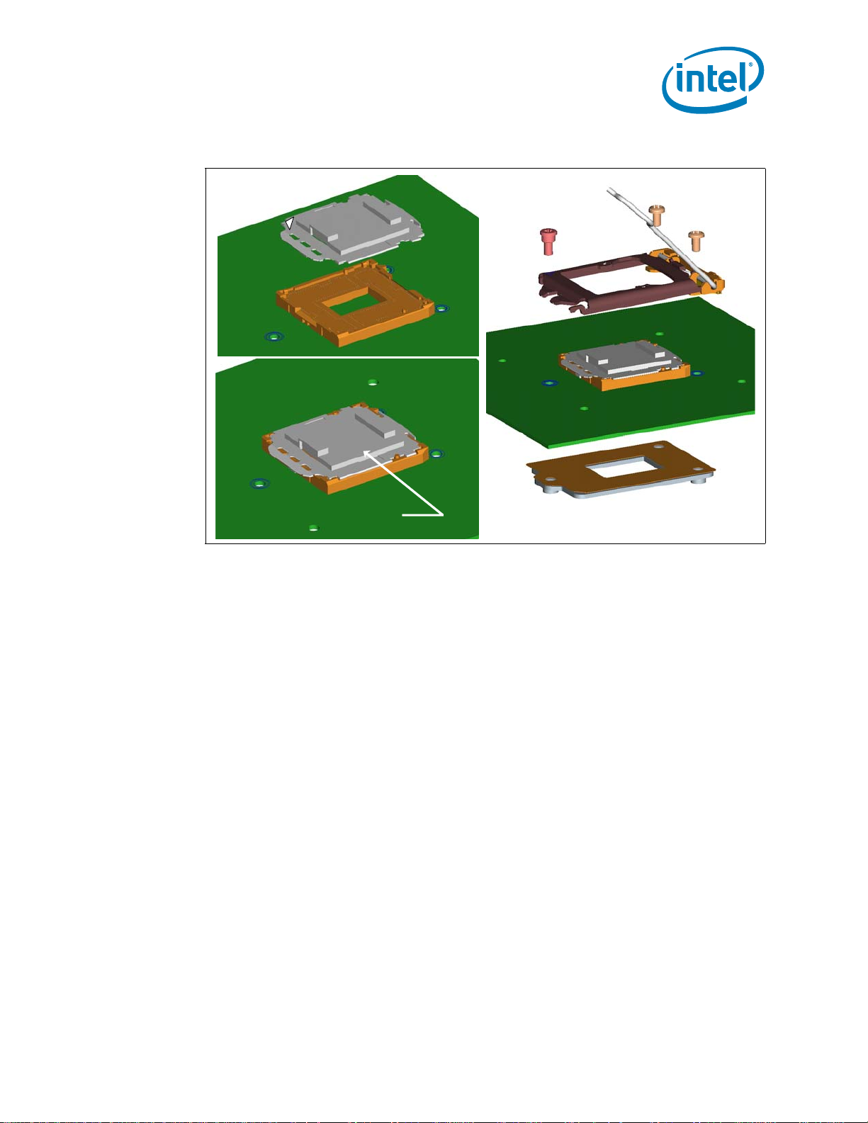
3-1 LGA1156 Socket with Pick and Place Cover..............................................................17
3-2 LGA1156 Socket Contact Numbering (Top View of Socket).........................................18
3-3 LGA1156 Socket Land Pattern (Top View of Board) ...................................................19
3-4 LGA1156 Socket NCTF Solder Joints .......................................................................20
3-5 Attachment to Motherboard...................................................................................21
3-6 Pick and Place Cover.............................................................................................23
3-7 Package Installation / Removal Features .................................................................24
4-1 ILM Cover Assembly .............................................................................................28
4-2 Back Plate...........................................................................................................28
4-3 Shoulder Screw....................................................................................................29
4-4 ILM Assembly ......................................................................................................30
4-5 Pin 1 and ILM Lever..............................................................................................31
5-1 Flow Chart of Knowledge-Based Reliability Evaluation Methodology.............................36
6-1 Thermal Test Vehicle Thermal Profile for Intel
6-2 Thermal Test Vehicle Thermal Profile for Intel® Xeon® Processor 3400 Series (45W) .....41
6-3 TTV Case Temperature (TCASE) Measurement Location.............................................44
6-4 Frequency and Voltage Ordering ............................................................................46
6-5 Temperature Sensor Data Format...........................................................................49
7-1 Comparison of Case Temperature versus Sensor Based Specification...........................52
7-2 Intel
®
Xeon® Processor 3400 Series (95W) Thermal Profile........................................53
7-3 Required YCA for Various TAMBIENT Conditions........................................................55
8-1 1U Heatsink Performance Curves............................................................................60
8-2 1U Heatsink Performance Curves............................................................................61
8-3 1U Collaboration Heatsink Assembly .......................................................................63
8-4 KOZ 3-D Model (Top) in 1U Server .........................................................................64
10-1 Boxed Processor Fan Heatsink................................................................................69
10-2 Space Requirements for the Boxed Processor (side view)...........................................70
10-3 Space Requirements for the Boxed Processor (top view)............................................71
10-4 Space Requirements for the Boxed Processor (overall view) .......................................71
10-5 Boxed Processor Fan Heatsink Power Cable Connector Description ..............................72
10-6 Baseboard Power Header Placement Relative to Processor Socket ...............................73
10-7 Boxed Processor Fan Heatsink Airspace Keepout Requirements (top view) ...................74
10-8 Boxed Processor Fan Heatsink Airspace Keepout Requirements (side view) ..................74
10-9 Boxed Processor Fan Heatsink Set Points.................................................................75
B-1 Socket / Heatsink / ILM Keepout Zone Primary Side for 1U(Top).................................80
B-2 Socket / Heatsink / ILM Keepout Zone Secondary Side for 1U(Bottom)........................81
®
Xeon® Processor 3400 Series (95W) .....39
4 Thermal/Mechanical Specifications and Design Guidelines
Page 5

B-3 Socket / Processor / ILM Keepout Zone Primary Side for 1U(Top)............................... 82
B-4 Socket / Processor / ILM Keepout Zone Secondary Side for 1U(Bottom) ...................... 83
B-5 1U Collaboration Heatsink Assembly.......................................................................84
B-6 1U Collaboration Heatsink..................................................................................... 85
B-7 1U Collaboration Heatsink Screw............................................................................ 86
B-8 Heatsink Compression Spring ................................................................................87
B-9 Heatsink Load Cup ............................................................................................... 88
B-10 Heatsink Retaining Ring........................................................................................ 89
B-11 Heatsink Backplate Assembly ................................................................................90
B-12 Heatsink Backplate .............................................................................................. 91
B-13 Heatsink Backplate Insulator ................................................................................. 92
B-14 Heatsink Backplate Stud ....................................................................................... 93
B-15 Thermocouple Attach Drawing ...............................................................................94
B-16 1U ILM Shoulder Screw ........................................................................................ 95
B-17 1U ILM Standard 6-32 Thread Fastener...................................................................96
C-1 Socket Mechanical Drawing (Sheet 1 of 4)...............................................................98
C-2 Socket Mechanical Drawing (Sheet 2 of 4)...............................................................99
C-3 Socket Mechanical Drawing (Sheet 3 of 4)............................................................. 100
C-4 Socket Mechanical Drawing (Sheet 4 of 4)............................................................. 101
D-1 Processor Package Drawing (Sheet 1 of 2) ............................................................ 104
D-2 Processor Package Drawing (Sheet 2 of 2) ............................................................ 105
Tables
1-1 Reference Documents.............................................................................................7
1-2 Terms and Descriptions ..........................................................................................8
2-1 Processor Loading Specifications............................................................................ 13
2-2 Package Handling Guidelines ................................................................................. 13
2-3 Processor Materials .............................................................................................. 14
2-4 Storage Conditions............................................................................................... 16
5-1 Socket Component Mass....................................................................................... 33
5-2 1156-land Package and LGA1156 Socket Stackup Height .......................................... 33
5-3 Socket & ILM Mechanical Specifications................................................................... 34
5-4 Electrical Requirements for LGA1156 Socket............................................................ 35
6-1 Intel
6-2 Thermal Test Vehicle Thermal Profile for Intel® Xeon® Processor 3400 Series (95W) .... 40
6-3 Thermal Test Vehicle Thermal Profile for Intel
6-4 Thermal Solution Performance above TCONTROL for the Intel
6-5 Thermal Solution Performance above TCONTROL for the Intel
6-6 Supported PECI Command Functions and Codes ...................................................... 49
6-7 Error Codes and Descriptions................................................................................. 50
8-1 Boundary Conditions and Performance Targets ........................................................ 59
8-2 Comparison between TTV Thermal Profile and Thermal Solution Performance
9-1 Use Conditions (Board Level)................................................................................. 65
10-1 Fan Heatsink Power and Signal Specifications .......................................................... 73
10-2 Fan Heatsink Set Points ........................................................................................ 75
A-1 Collaboration Heatsink Enabled Components ........................................................... 77
A-2 LGA1156 Socket and ILM Components.................................................................... 77
A-3 Supplier Contact Information................................................................................. 77
B-1 Mechanical Drawing List........................................................................................ 79
C-1 Mechanical Drawing List........................................................................................ 97
D-1 Mechanical Drawing List...................................................................................... 103
®
Xeon® Processor 3400 Series Thermal Specifications ...................................... 38
®
Xeon® Processor 3400 Series (45W) .... 41
Processor 3400 Series (95W) ................................................................................42
®
Xeon®
®
Xeon®
Processor 3400 Series (45W) ................................................................................43
®
for Intel
Xeon® Processor 3400 Series (95W) ........................................................ 61
Thermal/Mechanical Specifications and Design Guidelines 5
Page 6

Document
Number
322374 -001 • Initial release September 2009
Revision
Number
Description Revision Date
§
6 Thermal/Mechanical Specifications and Design Guidelines
Page 7
Introduction
1 Introduction
This document differs from previous Thermal and Mechanical Design Guidelines. In this
document, mechanical and thermal specifications for the processor and the associated
socket are now included. The usual design guidance has been retained.
The components described in this document include:
• The thermal and mechanical specifications for the
—Intel® Xeon® processor 3400 series
• The LGA1156 socket and the Independent Loading Mechanism (ILM) and back
plate.
• The collaboration design thermal solution (heatsink) for the processors and
associated retention hardware.
®
The Intel
for clarity this document will use Intel® Xeon® processor 3400 series (95W) or Intel
Xeon® processor 3400 series (45W).
Xeon® processor 3400 series has two thermal specifications. When required
®
Note: For Workstation segment, since boundary conditions, ILM assembly and reference
thermal solution etc. are similar to Desktop’s corresponding parts, user could refer to
®
Intel
Core™ i7-800 and i5-700 Desktop Processor Series and LGA1156 Socket
Thermal/Mechanical Specifications and Design Guidelines.
Note: When the information is applicable to all products, the this document will use
“processor” or “processors” to simplify the document.
1.1 References
Material and concepts available in the following documents may be beneficial when
reading this document.
Table 1-1. Reference Documents
Document Location
®
Xeon® Processor 3400 Series Datasheet, Volume 1
Intel
®
Intel
Xeon® Processor 3400 Series Datasheet, Volume 2
®
Intel
Xeon® Processor 3400 Series Specification Update www.intel.com/Assets/
®
5 Series Chipset and Intel® 3400 Chipset Datasheet www.intel.com/Assets/
Intel
®
Intel
5 Series Chipset and Intel® 3400 Chipset Specification Update www.intel.com/Assets/
®
5 Series Chipset and Intel® 3400 Chipset – Thermal Mechanical
Intel
Specifications and Design Guidelines
4-Wire Pulse Width Modulation (PWM) Controlled Fans http://
www.intel.com/Assets/
PDF/datasheet/322371.pdf
www.intel.com/Assets/
PDF/datasheet/322372.pdf
PDF/specupdate/
322173.pdf
PDF/datasheet/322169.pdf
PDF/specupdate/
322170.pdf
www.intel.com/Assets/
PDF/designguide/
322171.pdf
www.formfactors.org/
Thermal/Mechanical Specifications and Design Guidelines 9
Page 8
1.2 Definition of Terms
Table 1-2. Terms and Descriptions (Sheet 1 of 2)
Term Description
Bypass Bypass is the area between a passive heatsink and any object that can act to form a
CTE Coefficient of Thermal Expansion. The relative rate a material expands during a thermal
DTS Digital Thermal Sensor reports a relative die temperature as an offset from TCC
FSC Fan Speed Control
IHS Integrated Heat Spreader: a component of the processor package used to enhance the
ILM Independent Loading Mechanism provides the force needed to seat the 1156-LGA land
PCH Platform Controller Hub. The PCH is connected to the processor via the Direct Media
LGA1156 socket The processor mates with the system board through this surface mount, 1156-land
PECI The Platform Environment Control Interface (PECI) is a one-wire interface that provides
Ψ
CA
Ψ
CS
Ψ
SA
T
CASE or TC
T
CASE_MAX
TCC Thermal Control Circuit: Thermal monitor uses the TCC to reduce the die temperature by
T
CONTROL
TDP Thermal Design Power: Thermal solution should be designed to dissipate this target
Thermal Monitor A power reduction feature designed to decrease temperature after the processor has
Thermal Profile Line that defines case temperature specification of the TTV at a given power level.
TIM Thermal Interface Material: The thermally conductive compound between the heatsink
duct. For this example, it can be expressed as a dimension away from the outside
dimension of the fins to the nearest surface.
event.
activation temperature.
thermal performance of the package. Component thermal solutions interface with the
processor at the IHS surface.
package onto the socket contacts.
®
Interface (DMI) and Intel
Flexible Display Interface (Intel® FDI).
socket.
a communication channel between Intel processor and chipset components to external
monitoring devices.
Case-to-ambient thermal characterization parameter (psi). A measure of thermal
solution performance using total package power. Defined as (T
Package Power. The heat source should always be specified for Ψ measurements.
Case-to-sink thermal characterization parameter. A measure of thermal interface
material performance using total package power. Defined as (T
Power.
Sink-to-ambient thermal characterization parameter. A measure of heatsink thermal
performance using total package power. Defined as (T
The case temperature of the processor, measured at the geometric center of the topside
of the TTV IHS.
The maximum case temperature as specified in a component specification.
using clock modulation and/or operating frequency and input voltage adjustment when
the die temperature is very near its operating limits.
T
trigger point for fan speed control. When DTS > T
with the TTV thermal profile.
is a static value that is below the TCC activation temperature and used as a
CONTROL
power level. TDP is not the maximum power that the processor can dissipate.
reached its maximum operating temperature.
and the processor case. This material fills the air gaps and voids, and enhances the
transfer of the heat from the processor case to the heatsink.
– TLA) / Total
CASE
– TS) / Total Package
CASE
– TLA) / Total Package Power.
S
, the processor must comply
CONTROL
Introduction
10 Thermal/Mechanical Specifications and Design Guidelines
Page 9
Introduction
Table 1-2. Terms and Descriptions (Sheet 2 of 2)
Term Description
TTV Thermal Test Vehicle. A mechanically equivalent package that contains a resistive heater
T
LA
T
SA
in the die to evaluate thermal solutions.
The measured ambient temperature locally surrounding the processor. The ambient
temperature should be measured just upstream of a passive heatsink or at the fan inlet
for an active heatsink.
The system ambient air temperature external to a system chassis. This temperature is
usually measured at the chassis air inlets.
§
Thermal/Mechanical Specifications and Design Guidelines 11
Page 10

Introduction
12 Thermal/Mechanical Specifications and Design Guidelines
Page 11
Package Mechanical and Storage Specifications
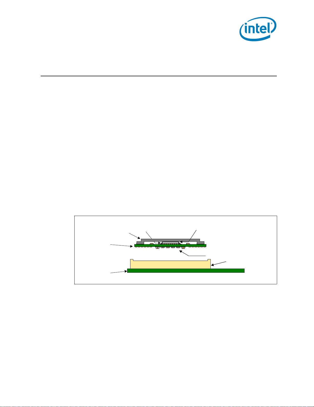
IHS
Substrate
System Board
Capacitors
Core (die)
TIM
LGA1156 Socket
2 Package Mechanical and
Storage Specifications
2.1 Package Mechanical Specifications
The processor is packaged in a Flip-Chip Land Grid Array package that interfaces with
the motherboard via the LGA1156 socket. The package consists of a processor
mounted on a substrate land-carrier. An integrated heat spreader (IHS) is attached to
the package substrate and core and serves as the mating surface for processor thermal
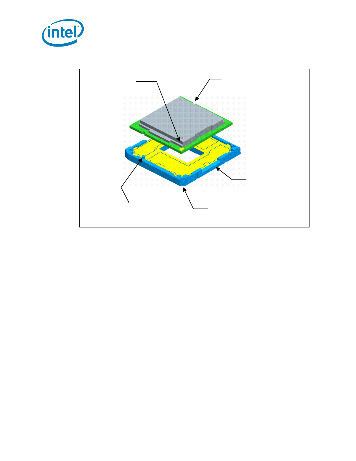
solutions, such as a heatsink. Figure 2-1 shows a sketch of the processor package
components and how they are assembled together. Refer to Chapter 3 and Chapter 4
for complete details on the LGA1156 socket.
The package components shown in Figure 2-1 include the following:
1. Integrated Heat Spreader (IHS)
2. Thermal Interface Material (TIM)
3. Processor core (die)
4. Package substrate
5. Capacitors
Figure 2-1. Processor Package Assembly Sketch
Note:
1. Socket and motherboard are included for reference and are not part of processor package.
2. For clarity the ILM is not shown.
Thermal/Mechanical Specifications and Design Guidelines 13
Page 12
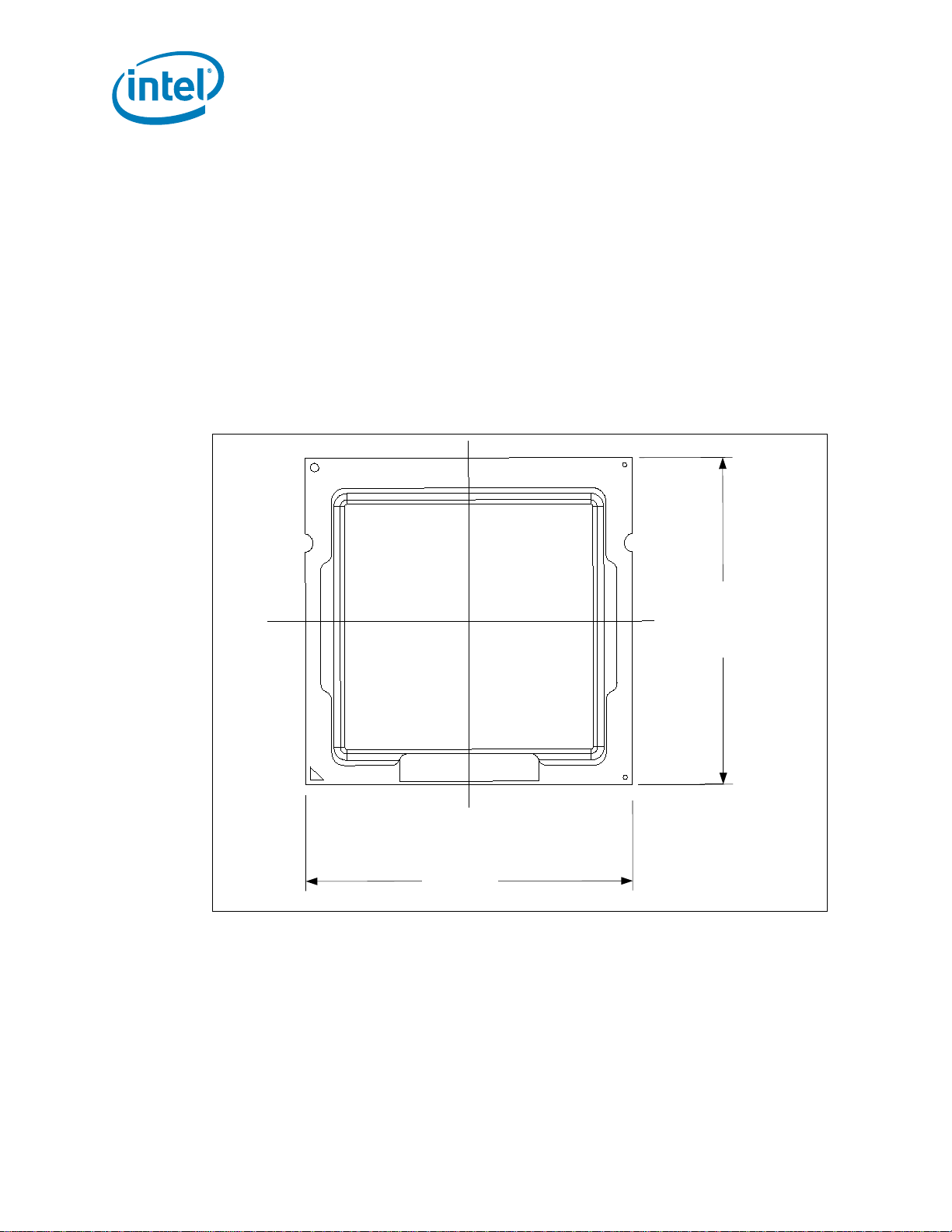
2.1.1 Package Mechanical Drawing
37.5
37.5
Figure 2-2 shows the basic package layout and dimensions. The detailed package
mechanical drawings are in Appendix D. The drawings include dimensions necessary to
design a thermal solution for the processor. These dimensions include:
1. Package reference dimensions with tolerances (total height, length, width, and so
forth.)
2. IHS parallelism and tilt
3. Land dimensions
4. Top-side and back-side component keep-out dimensions
5. Reference datums
6. All drawing dimensions are in mm.
Figure 2-2. Package View
Package Mechanical and Storage Specifications
2.1.2 Processor Component Keep-Out Zones
The processor may contain components on the substrate that define component keepout zone requirements. A thermal and mechanical solution design must not intrude into
the required keep-out zones. Decoupling capacitors are typically mounted to either the
topside or land-side of the package substrate. See Figure B-3 and Figure B-4 for keepout zones. The location and quantity of package capacitors may change due to
manufacturing efficiencies but will remain within the component keep-in. This keep-in
zone includes solder paste and is a post reflow maximum height for the components.
14 Thermal/Mechanical Specifications and Design Guidelines
Page 13
Package Mechanical and Storage Specifications
2.1.3 Package Loading Specifications
Tab l e 2- 1 provides dynamic and static load specifications for the processor package.
These mechanical maximum load limits should not be exceeded during heatsink
assembly, shipping conditions, or standard use condition. Also, any mechanical system
or component testing should not exceed the maximum limits. The processor package
substrate should not be used as a mechanical reference or load-bearing surface for
.
Table 2-1. Processor Loading Specifications
thermal and mechanical solution.
Parameter Minimum Maximum Notes
Static Compressive Load — 600 N [135 lbf] 1, 2, 3
Dynamic Compressive
Notes:
1. These specifications apply to uniform compressive loading in a direction normal to the processor IHS.
2. This is the maximum static force that can be applied by the heatsink and retention solution to maintain the
3. These specifications are based on limited testing for design characterization. Loading limits are for the
4. Dynamic loading is defined as an 50g shock load, 2X Dynamic Acceleration Factor with a 500g maximum
Load
heatsink and processor interface.
package only and do not include the limits of the processor socket.
thermal solution.
— 712 N [160 lbf] 1, 3, 4
2.1.4 Package Handling Guidelines
Tab l e 2- 2 includes a list of guidelines on package handling in terms of recommended
maximum loading on the processor IHS relative to a fixed substrate. These package
handling loads may be experienced during heatsink removal.
Table 2-2. Package Handling Guidelines
Parameter Maximum Recommended Notes
Shear 311 N [70 lbf] 1, 4
Tensile 111 N [25 lbf] 2, 4
Torque 3.95 N-m [35 lbf-in] 3, 4
Notes:
1. A shear load is defined as a load applied to the IHS in a direction parallel to the IHS top surface.
2. A tensile load is defined as a pulling load applied to the IHS in a direction normal to the IHS surface.
3. A torque load is defined as a twisting load applied to the IHS in an axis of rotation normal to the IHS top
surface.
4. These guidelines are based on limited testing for design characterization.
2.1.5 Package Insertion Specifications
The processor can be inserted into and removed from an LGA1156 socket 15 times. The
socket should meet the LGA1156 socket requirements detailed in Chapter 5.
2.1.6 Processor Mass Specification
The typical mass of the processor is 21.5g (0.76 oz). This mass [weight] includes all
the components that are included in the package.
Thermal/Mechanical Specifications and Design Guidelines 15
Page 14
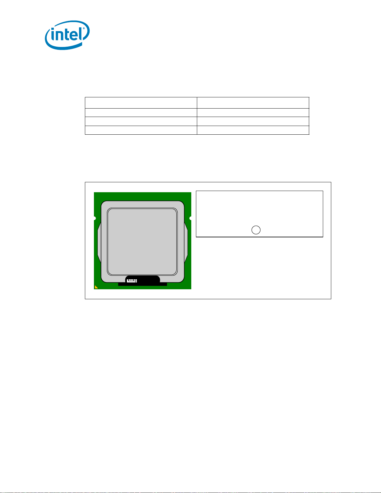
2.1.7 Processor Materials
Legend:
GRP1LINE1
GRP1LINE2
GRP1LINE3
GRP1LINE4
GRP1LINE5
Mark Text (Production Mark):
INTEL{M}{C}'08 PROC#
BRAND
SLxxx C00
SPEED/CACHE/ FMB
FPO
Legend:
GRP1LINE1
GRP1LINE2
GRP1LINE3
GRP1LINE4
GRP1LINE5
Mark Text (Engineering Mark):
INTEL{M}{C}'08
INTEL CONFIDENTIAL
Qxxx ES C00
PRODUCT CODE
FPO
e4
e4
GRP1LINE1
GRP1LINE2
GRP1LINE3
GRP1LINE4
GRP1LINE5
GRP1LINE1
GRP1LINE2
GRP1LINE3
GRP1LINE4
GRP1LINE5
LOT NO S/N
Package Mechanical and Storage Specifications
Tabl e 2 - 3 lists some of the package components and associated materials.
Table 2-3. Processor Materials
Component Material
Integrated Heat Spreader (IHS) Nickel Plated Copper
Substrate Fiber Reinforced Resin
Substrate Lands Gold Plated Copper
2.1.8 Processor Markings
Figure 2-3 shows the topside markings on the processor. This diagram is to aid in the
identification of the processor.
Figure 2-3. Processor Top-Side Markings
16 Thermal/Mechanical Specifications and Design Guidelines
Page 15
Package Mechanical and Storage Specifications
AY
AV
AT
AP
AM
AK
AH
AF
AD
AB
Y
V
T
P
M
K
H
F
D
B
AW
AU
AR
AN
AL
AJ
AG
AE
AC
AA
W
U
N
R
K
J
G
E
C
A
1 3 5 7 9 11 13 15 17 19 21 23 25 27 29 31
33 35 37 39
2 4 6 8 10 12 14 16 18 20 22 24 26 28 30 32
34 36 38 40
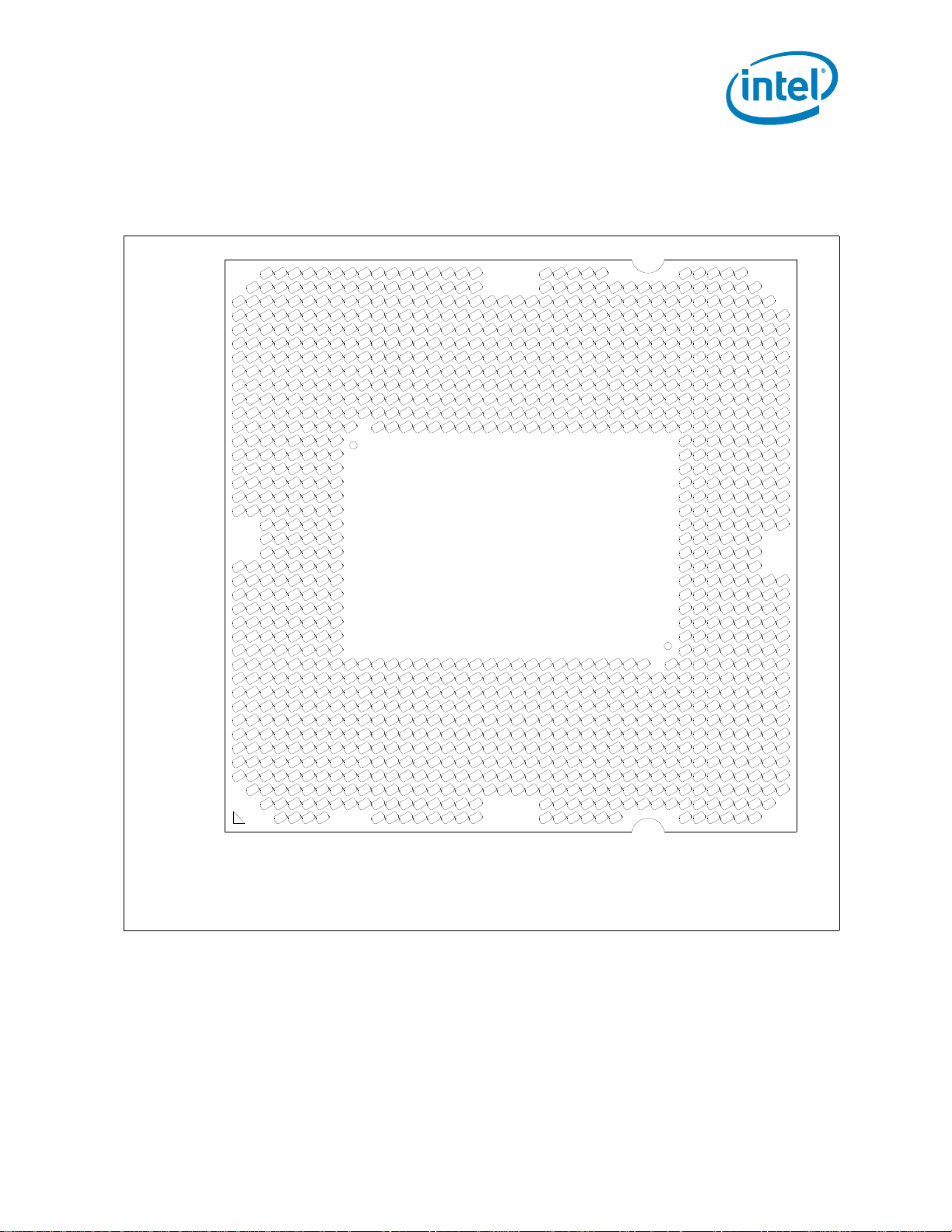
2.1.9 Processor Land Coordinates
.
Figure 2-4. Processor Package Lands Coordinates
Thermal/Mechanical Specifications and Design Guidelines 17
Figure 2-4 shows the bottom view of the processor package.
Page 16
Package Mechanical and Storage Specifications
2.2 Processor Storage Specifications
Tabl e 2 - 4 includes a list of the specifications for device storage in terms of maximum
and minimum temperatures and relative humidity. These conditions should not be
.
Table 2-4. Storage Conditions
exceeded in storage or transportation.
Parameter Description Min Max Notes
T
ABSOLUTE STORAGE
T
SUSTAINED STORAGE
RH
SUSTAINED STORAGE
TIME
SUSTAINED STORAGE
Notes:
1. Refers to a component device that is not assembled in a board or socket that is not to be electrically
connected to a voltage reference or I/O signals.
2. Specified temperatures are based on data collected. Exceptions for surface mount reflow are specified in
applicable JEDEC standard and MAS document. Non-adherence may affect processor reliability.
3. T
ABSOLUTE STORAGE
moisture barrier bags or desiccant.
®
4. Intel
5. The JEDEC, J-JSTD-020 moisture level rating and associated handling practices apply to all moisture
6. Nominal temperature and humidity conditions and durations are given and tested within the constraints
branded board products are certified to meet the following temperature and humidity limits that are
given as an example only (Non-Operating Temperature Limit: -40 °C to 70 °C, Humidity: 50% to 90%,
non-condensing with a maximum wet bulb of 28 °C). Post board attach storage temperature limits are not
specified for non-Intel branded boards.
sensitive devices removed from the moisture barrier bag.
imposed by T
SUSTAINED
The non-operating device storage
temperature. Damage (latent or otherwise)
may occur when subjected to for any length of
time.
The ambient storage temperature limit (in
shipping media) for a sustained period of time.
The maximum device storage relative humidity
for a sustained period of time.
A prolonged or extended period of time;
typically associated with customer shelf life. 0 Months6 Months
applies to the unassembled component only and does not apply to the shipping media,
and customer shelf life in applicable Intel box and bags.
-55 °C 125 °C 1, 2, 3
-5 °C 40 °C 4, 5
60% @ 24 °C 5, 6
6
§
18 Thermal/Mechanical Specifications and Design Guidelines
Page 17

LGA1156 Socket
3 LGA1156 Socket
This chapter describes a surface mount, LGA (Land Grid Array) socket intended for the
processors. The socket provides I/O, power, and ground contacts. The socket contains
1156 contacts arrayed about a cavity in the center of the socket with lead-free solder
balls for surface mounting on the motherboard.
The contacts are arranged in two opposing L-shaped patterns within the grid array. The
grid array is 40 x 40 with 24 x 16 grid depopulation in the center of the array and
selective depopulation elsewhere.
The socket must be compatible with the package (processor) and the Independent
Loading Mechanism (ILM). The ILM design includes a back plate that is integral to
having a uniform load on the socket solder joints. Socket loading specifications are
listed in Chapter 5.
Figure 3-1. LGA1156 Socket with Pick and Place Cover
Thermal/Mechanical Specifications and Design Guidelines 19
Page 18
Figure 3-2. LGA1156 Socket Contact Numbering (Top View of Socket)
A C E G J L N R U W AA AC AE AG AJ AL AN AR AU AW
B D F H K M P T V Y AB AD AF
AH AK
AM AP AT AV AY
1
3
7
5
9
11
15
13
17
19
23
21
25
27
29
2
8
4
6
10
16
12
14
18
24
20
22
26
28
30
15
11
13
17
23
19
21
25
31
27
29
33
39
35
37
32
14
12
16
18
22
20
24
26
30
28
34
38
36
40
A C E G J L N R U W AA AC AE AG AJ AL AN AR AU AW
B D F H K M P T V Y AB AD AF
AH AK
AM AP AT AV AY
1
3
7
5
9
11
15
13
17
19
23
21
25
27
29
2
8
4
6
10
16
12
14
18
24
20
22
26
28
30
15
11
13
17
23
19
21
25
31
27
29
33
39
35
37
32
14
12
16
18
22
20
24
26
30
28
34
38
36
40
A C E G J L N R U W AA AC AE AG AJ AL AN AR AU AWA C E G J L N R U W AA AC AE AG AJ AL AN AR AU AW
B D F H K M P T V Y AB AD AF
AH AK
AM AP AT AV AY
B D F H K M P T V Y AB AD AF
AH AK
AM AP AT AV AY
1
3
7
5
9
11
15
13
17
19
23
21
25
27
29
1
3
7
5
9
11
15
13
17
19
23
21
25
27
29
2
8
4
6
10
16
12
14
18
24
20
22
26
28
30
2
8
4
6
10
16
12
14
18
24
20
22
26
28
30
15
11
13
17
23
19
21
25
31
27
29
33
39
35
37
15
11
13
17
23
19
21
25
31
27
29
33
39
35
37
32
14
12
16
18
22
20
24
26
30
28
34
38
36
40
32
14
12
16
18
22
20
24
26
30
28
34
38
36
40
LGA1156 Socket
20 Thermal/Mechanical Specifications and Design Guidelines
Page 19
LGA1156 Socket
A C E G J L N R U W AA ACAEAGAJ ALANAR AUAW
B D F H K M P T V Y AB AD AF AH AK AM AP AT AV AY
1
3
7
5
9
11
15
13
17
19
23
21
25
27
29
2
8
4
6
10
16
12
14
18
24
20
22
26
28
30
32
15
11
14
12
13
16
17
23
19
18
22
20
21
24
25
31
27
26
30
28
29
33
39
35
34
38
36
37
40
B D F H K M P T V Y AB AD AF AH AK AM AP AT AV AY
A C E G J L N R U W AA AC AE A G AJ AL A N AR AU AW
122.6 mil (3.1144mm)
36mil (0.9144 mm)
A C E G J L N R U W AA ACAEAGAJ ALANAR AUAW
B D F H K M P T V Y AB AD AF AH AK AM AP AT AV AY
1
3
7
5
9
11
15
13
17
19
23
21
25
27
29
1
3
7
5
9
11
15
13
17
19
23
21
25
27
29
2
8
4
6
10
16
12
14
18
24
20
22
26
28
30
2
8
4
6
10
16
12
14
18
24
20
22
26
28
30
32
15
11
14
12
13
16
17
23
19
18
22
20
21
24
25
31
27
26
30
28
29
33
39
35
34
38
36
37
40
B D F H K M P T V Y AB AD AF AH AK AM AP AT AV AY
A C E G J L N R U W AA AC AE A G AJ AL A N AR AU AW
122.6 mil (3.1144mm)
36mil (0.9144 mm)
3.1 Board Layout
The land pattern for the LGA1156 socket is 36 mils X 36 mils (X by Y) within each of the
two L-shaped sections. Note that there is no round-off (conversion) error between
socket pitch (0.9144 mm) and board pitch (36 mil) as these values are equivalent. The
two L-sections are offset by 0.9144 mm (36 mil) in the x direction and 3.114 mm
(122.6 mil) in the y direction (see Figure 3-3). This was to achieve a common package
land to PCB land offset that ensures a single PCB layout for socket designs from the
multiple vendors.
Figure 3-3. LGA1156 Socket Land Pattern (Top View of Board)
Thermal/Mechanical Specifications and Design Guidelines 21
Page 20
3.2 LGA1156 Socket NCTF Solder Joints
1
3
7
5
9
11
15
13
17
19
23
21
25
27
29
2
8
4
6
10
16
12
14
18
24
20
22
26
28
30
A C E G J L N R U W AA AC AE AG AJ AL AN AR AU AW
B D F H K M P T V Y AB AD AF AH AK AM AP AT AV AY
32
15
11
14
12
13
16
17
23
19
18
22
20
21
24
25
31
27
26
30
28
29
33
39
35
34
38
36
37
40
A C E G J L N R U W AA AC AE AG AJ AL AN AR AU AW
B D F H K M P T V Y AB AD AF AH AK AM AP AT AV AY
20 mil corner NCTF
20 mil corner CTF
14 x 18 mil oval pads
16.9 mil circular pads
Intel has defined selected solder joints of the socket as non-critical to function (NCTF)
when evaluating package solder joints post environmental testing. The signals at NCTF
locations are typically redundant ground or non-critical reserved, so the loss of the
solder joint continuity at end of life conditions will not affect the overall product
functionality. Figure 3-4 identifies the NCTF solder joints.
Figure 3-4. LGA1156 Socket NCTF Solder Joints
LGA1156 Socket
22 Thermal/Mechanical Specifications and Design Guidelines
Page 21

LGA1156 Socket
Load plate
Frame
Load Lever
Back Plate
Shoulder
Screw
Load plate
Frame
Load Lever
Back Plate
Shoulder
Screw
3.3 Attachment to Motherboard
The socket is attached to the motherboard by 1156 solder balls. There are no additional
external methods (that is, screw, extra solder, adhesive, etc.) to attach the socket.
As indicated in Figure 3-1, the Independent Loading Mechanism (ILM) is not present
during the attach (reflow) process.
Figure 3-5. Attachment to Motherboard
3.4 Socket Components
The socket has two main components, the socket body and Pick and Place (PnP) cover,
and is delivered as a single integral assembly. Refer to Appendix C for detailed
drawings.
3.4.1 Socket Body Housing
The housing material is thermoplastic or equivalent with UL 94 V-0 flame rating capable
of withstanding 260 °C for 40 seconds, which is compatible with typical reflow/rework
profiles. The socket coefficient of thermal expansion (in the XY plane), and creep
properties, must be such that the integrity of the socket is maintained for the
conditions listed in Chapter 5.
The color of the housing will be dark as compared to the solder balls to provide the
contrast needed for pick and place vision systems.
Thermal/Mechanical Specifications and Design Guidelines 23
Page 22

3.4.2 Solder Balls
A total of 1156 solder balls corresponding to the contacts are on the bottom of the
socket for surface mounting with the motherboard. The socket solder ball has the
following characteristics:
• Lead free SAC (SnAgCu) 305 solder alloy with a silver (Ag) content between 3%
and 4% and a melting temperature of approximately 217 °C. The alloy must be
compatible with immersion silver (ImAg) and Organic Solderability Protectant
(OSP) motherboard surface finishes and a SAC alloy solder paste.
The co-planarity (profile) and true position requirements are defined in Appendix C.
3.4.3 Contacts
Base material for the contacts is high strength copper alloy.
For the area on socket contacts where processor lands will mate, there is a 0.381 μm
[15 μinches] minimum gold plating over 1.27 μm [50 μinches] minimum nickel
underplate.
No contamination by solder in the contact area is allowed during solder reflow.
LGA1156 Socket
3.4.4 Pick and Place Cover
The cover provides a planar surface for vacuum pick up used to place components in
the Surface Mount Technology (SMT) manufacturing line. The cover remains on the
socket during reflow to help prevent contamination during reflow. The cover can
withstand 260 °C for 40 seconds (typical reflow/rework profile) and the conditions
listed in Chapter 5 without degrading.
As indicated in Figure 3-6, the cover remains on the socket during ILM installation, and
should remain on whenever possible to help prevent damage to the socket contacts.
Cover retention must be sufficient to support the socket weight during lifting,
translation, and placement (board manufacturing), and during board and system
shipping and handling. Covers can be removed without tools.
The socket vendors have a common interface on the socket body where the PnP cover
attaches to the socket body. This should allow the PnP covers to be compatible between
socket suppliers.
As indicated in Figure 3-6, a Pin1 indicator on the cover provides a visual reference for
proper orientation with the socket.
24 Thermal/Mechanical Specifications and Design Guidelines
Page 23
LGA1156 Socket
Pick & Place Cover
Pin 1
ILM Installation
Pick & Place Cover
Pin 1
ILM Installation
Figure 3-6. Pick and Place Cover
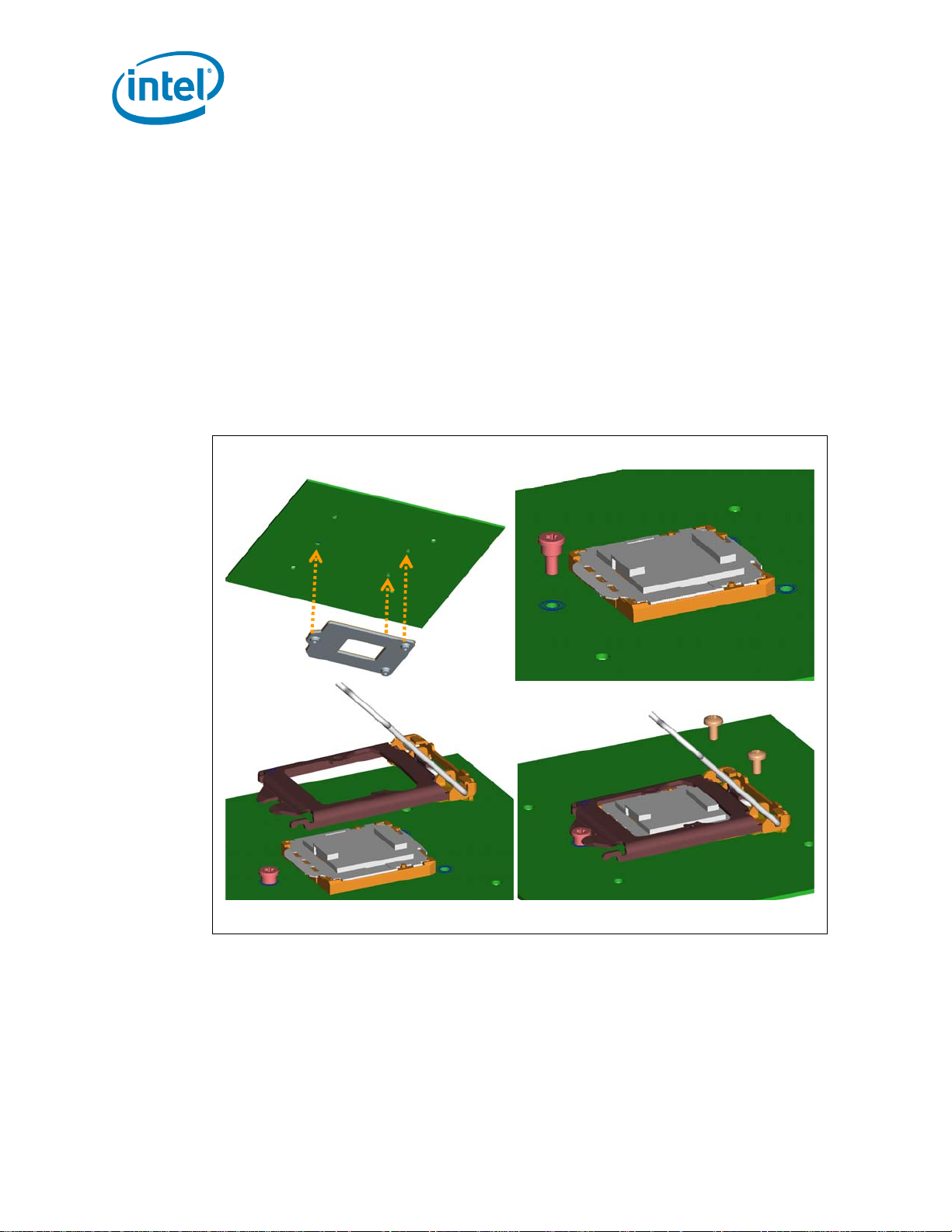
3.5 Package Installation / Removal
As indicated in Figure 3-7, access is provided to facilitate manual installation and
removal of the package.
To assist in package orientation and alignment with the socket:
• The package Pin 1 triangle and the socket Pin1 chamfer provide visual reference for
proper orientation.
• The package substrate has orientation notches along two opposing edges of the
package, offset from the centerline. The socket has two corresponding orientation
posts to physically prevent mis-orientation of the package. These orientation
features also provide initial rough alignment of package to socket.
• The socket has alignment walls at the four corners to provide final alignment of the
package.
Thermal/Mechanical Specifications and Design Guidelines 25
Page 24
.
Pin 1
Chamfer
Package
Pin 1
Indicator
Alignment
Post
(2 Places)
Finger
Access
(2 Places)
Orientation
Notch
(2 Places)
Figure 3-7. Package Installation / Removal Features
LGA1156 Socket
3.5.1 Socket Standoffs and Package Seating Plane
Standoffs on the bottom of the socket base establish the minimum socket height after
solder reflow and are specified in Appendix C.
Similarly, a seating plane on the top-side of the socket establishes the minimum
package height. See Section 5.2 for the calculated IHS height above the motherboard.
3.6 Durability
The socket must withstand 20 cycles of processor insertion and removal. The max
chain contact resistance from Tab l e 5- 4 must be met when mated in the 1st and 20th
cycles.
The socket Pick and Place cover must withstand 15 cycles of insertion and removal.
26 Thermal/Mechanical Specifications and Design Guidelines
Page 25

LGA1156 Socket
3.7 Markings
There are three markings on the socket:
• LGA1156: Font type is Helvetica Bold - minimum 6 point (2.125 mm).
• Manufacturer's insignia (font size at supplier's discretion).
• Lot identification code (allows traceability of manufacturing date and location).
All markings must withstand 260°C for 40 seconds (typical reflow/rework profile)
without degrading, and must be visible after the socket is mounted on the
motherboard.
LGA1156 and the manufacturer's insignia are molded or laser marked on the side wall.
3.8 Component Insertion Forces
Any actuation must meet or exceed SEMI S8-95 Safety Guidelines for Ergonomics/
Human Factors Engineering of Semiconductor Manufacturing Equipment, example Table
R2-7 (Maximum Grip Forces). The socket must be designed so that it requires no force
to insert the package into the socket.
3.9 Socket Size
Socket information needed for motherboard design is given in Appendix C.
This information should be used in conjunction with the reference motherboard keepout drawings provided in Appendix B to ensure compatibility with the reference thermal
mechanical components.
§
Thermal/Mechanical Specifications and Design Guidelines 27
Page 26

LGA1156 Socket
28 Thermal/Mechanical Specifications and Design Guidelines
Page 27

Independent Loading Mechanism (ILM)
4 Independent Loading
Mechanism (ILM)
The Independent Loading Mechanism (ILM) provides the force needed to seat the
1156-LGA land package onto the socket contacts. The ILM is physically separate from
the socket body. The assembly of the ILM to the board is expected to occur after wave
solder. The exact assembly location is dependent on manufacturing preference and test
flow. See the Manufacturing Advantage Service collateral for this platform for additional
guidance.
Note: The ILM has two critical functions: deliver the force to seat the processor onto the
socket contacts and distribute the resulting compressive load evenly through the socket
solder joints.
Note: The mechanical design of the ILM is integral to the overall functionality of the LGA1156
socket. Intel performs detailed studies on integration of processor package, socket and
ILM as a system. These studies directly impact the design of the ILM. The Intel
reference ILM will be “build to print” from Intel controlled drawings. Intel recommends
using the Intel Reference ILM. Custom non-Intel ILM designs do not benefit from Intel's
detailed studies and may not incorporate critical design parameters.
4.1 Design Concept
The ILM consists of two assemblies that will be procured as a set from the enabled
vendors. These two components are ILM cover assembly and back plate. To secure the
two assemblies, two types of fasteners are required a pair (2) of standard 6-32 thread
screws and a custom 6-32 thread shoulder screw. The reference design incorporates a
T-20 Torx* head fastener. The Torx* head fastener was chosen to ensure end users do
not inadvertently remove the ILM assembly and for consistency with the LGA1366
socket ILM. The Torx* head fastener is also less susceptible to driver slippage. Once
assembled the ILM is not required to be removed to install / remove the motherboard
from a chassis.
4.1.1 ILM Cover Assembly Design Overview
The ILM Cover assembly consists of three major pieces: load lever, load plate and the
hinge frame assembly.
All of the pieces in the ILM cover assembly except the hinge frame and the screws used
to attach the back plate are fabricated from stainless steel. The hinge frame is plated.
The frame provides the hinge locations for the load lever and load plate. An insulator is
pre-applied to the bottom surface of the hinge frame.
The cover assembly design ensures that once assembled to the back plate the only
features touching the board are the shoulder screw and the insulated hinge frame
assembly. The nominal gap of the load plate to the board is ~1 mm.
Thermal/Mechanical Specifications and Design Guidelines 29
Page 28
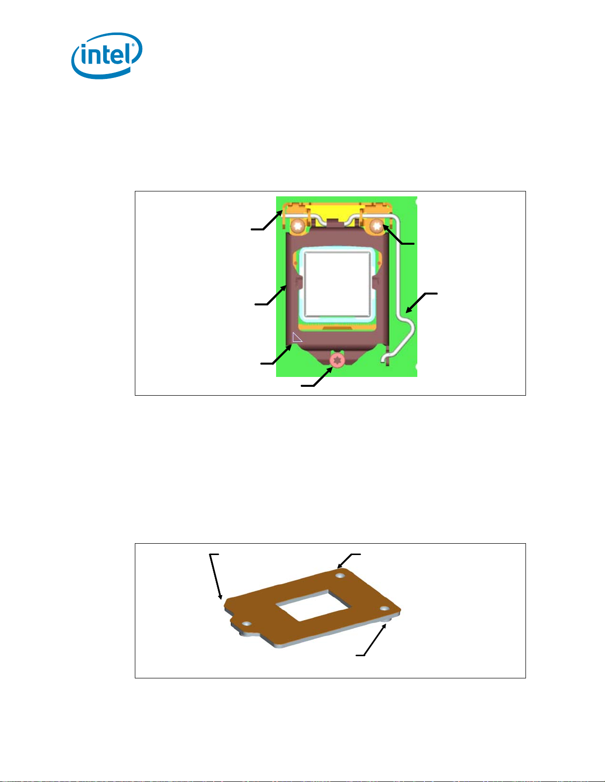
When closed, the load plate applies two point loads onto the IHS at the “dimpled”
Fasteners
Load
Lever
Load
Plate
Hinge /
Frame
Assy
Shoulder Screw
Pin 1 Indicator
Fasteners
Load
Lever
Load
Plate
Hinge /
Frame
Assy
Shoulder Screw
Pin 1 Indicator
Die Cut
Insulator
Pierced & Extruded
Thread Features
Assembly
Orientation
Feature
Die Cut
Insulator
Pierced & Extruded
Thread Features
Assembly
Orientation
Feature
features shown in Figure 4-1. The reaction force from closing the load plate is
transmitted to the hinge frame assembly and through the fasteners to the back plate.
Some of the load is passed through the socket body to the board inducing a slight
compression on the solder joints.
A pin 1 indicator will be marked on the ILM cover assembly.
Figure 4-1. ILM Cover Assembly
Independent Loading Mechanism (ILM)
4.1.2 ILM Back Plate Design Overview
The back plate (see Figure 4-2) is a flat steel back plate with pierced and extruded
features for ILM attach. A clearance hole is located at the center of the plate to allow
access to test points and backside capacitors if required. An insulator is pre-applied. A
notch is placed in one corner to assist in orienting the back plate during assembly.
Note: The Server ILM back plate is different from the Desktop design. Since Server
secondary-side clearance of 3.0 mm[0.118 inch] is generally available for leads and
backside components, so Server ILM back plate is designed with 1.8 mm thickness and
2.2 mm entire height including punch protrusion length.
Figure 4-2. Back Plate
30 Thermal/Mechanical Specifications and Design Guidelines
Page 29
Independent Loading Mechanism (ILM)
Shoulder
6-32 thread
Cap
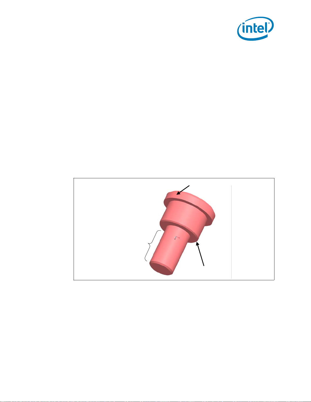
4.1.3 Shoulder Screw and Fasteners Design Overview
The shoulder screw is fabricated from carbonized steel rod. The shoulder height and
diameter are integral to the mechanical performance of the ILM. The diameter provides
alignment of the load plate. The height of the shoulder ensures the proper loading of
the IHS to seat the processor on the socket contacts. The design assumes the shoulder
screw has a minimum yield strength of 235 MPa.
A dimensioned drawing of the shoulder screw is available for local sourcing of this
component. Refer to Figure B-16 for the custom 6-32 thread shoulder screw drawing.
The standard fasteners can be sourced locally. The design assumes this fastener has a
minimum yield strength of 235 MPa. Refer to Figure B-17 for the standard 6-32 thread
fasteners drawing.
Note: The screws for Server ILM are different from Desktop design. The length of Server ILM
screws are shorter than the Desktop screw length to satisfy Server secondary-side
clearance limitation.
Note: The reference design incorporates a T-20 Torx* head fastener. The Torx* head fastener
was chosen to ensure end users do not inadvertently remove the ILM assembly and for
consistency with the LGA1366 socket ILM.
Figure 4-3. Shoulder Screw
Thermal/Mechanical Specifications and Design Guidelines 31
Page 30
Independent Loading Mechanism (ILM)
Step 1 Step 2
Step 3
Step 4
Step 1 Step 2
Step 3
Step 4
Step 1 Step 2
Step 3
Step 4
4.2 Assembly of ILM to a Motherboard
The ILM design allows a bottoms up assembly of the components to the board. See
Figure 4-4 for step by step assembly sequence.
1. Place the back plate in a fixture. The motherboard is aligned with the fixture.
2. Install the shoulder screw in the single hole near Pin 1 of the socket. Torque to a
minimum and recommended 8 inch-pounds, but not to exceed 10 inch-pounds.
3. Align and place the ILM cover assembly over the socket.
4. Install two (2) 6-32 fasteners. Torque to a minimum and recommended 8 inchpounds, but not to exceed 10 inch-pounds.
The thread length of the shoulder screw accommodates a nominal board thicknesses of
.
Figure 4-4. ILM Assembly
0.062”.
32 Thermal/Mechanical Specifications and Design Guidelines
Page 31

Independent Loading Mechanism (ILM)
Alignment
Features
Load plate not
shown for
clarity
Pin 1
Shoulder
Screw
Load
Lever
As indicated in Figure 4-5, the shoulder screw, socket protrusion and ILM key features
prevent 180 degree rotation of ILM cover assembly with respect to socket. The result is
a specific Pin 1 orientation with respect to ILM lever.
Figure 4-5. Pin 1 and ILM Lever
4.3 ILM Interchangeability
ILM cover assemblies and ILM back plates built from the Intel controlled drawings are
intended to be interchangeable. Interchangeability is defined as an ILM from Vendor A
will demonstrate acceptable manufacturability and reliability with a socket body from
Vendor A, B, or C. ILM cover assemblies and ILM back plates from all vendors are also
interchangeable.
The ILMs are an integral part of the socket validation testing. ILMs from each vendor
will be matrix tested with the socket bodies from each of the current vendors. The tests
would include manufacturability, bake and thermal cycling.
See Appendix A for vendor part numbers that were tested.
Note: Desktop and Server ILM backplate/screws are NOT interchangeable.
Note: ILMs that are not compliant with the Intel controlled ILM drawings can not be assured
to be interchangeable.
Thermal/Mechanical Specifications and Design Guidelines 33
Page 32

4.4 Markings
There are four markings on the ILM:
• 115XLM: Font type is Helvetica Bold - minimum 6 point (2.125 mm).
• Manufacturer's insignia (font size at supplier's discretion).
• Lot identification code (allows traceability of manufacturing date and location).
• Pin 1 indicator on the load plate.
All markings must be visible after the ILM is assembled on the motherboard.
115XLM and the manufacturer's insignia can be ink stamped or laser marked on the
side wall.
Independent Loading Mechanism (ILM)
§
34 Thermal/Mechanical Specifications and Design Guidelines
Page 33

LGA1156 Socket and ILM Electrical, Mechanical, and Environmental Specifications
5 LGA1156 Socket and ILM
Electrical, Mechanical, and
Environmental Specifications
This chapter describes the electrical, mechanical, and environmental specifications for
the LGA1156 socket and the Independent Loading Mechanism.
5.1 Component Mass
Table 5-1. Socket Component Mass
Component Mass
Socket Body, Contacts and PnP Cover 10 g
ILM Cover 29 g
ILM Back Plate 38 g
5.2 Package/Socket Stackup Height
Tab l e 5- 2 provides the stackup height of a processor in the 1156-land LGA package and
LGA1156 socket with the ILM closed and the processor fully seated in the socket.
Table 5-2. 1156-land Package and LGA1156 Socket Stackup Height
Component Stackup Height Note
Integrated Stackup Height
From Top of Board to Top of IHS
Socket Nominal Seating Plane Height 3.4 ± 0.2 mm 1
Package Nominal Thickness (lands to top of IHS) 4.381 ± 0.269 mm 1
Notes:
1. This data is provided for information only, and should be derived from: (a) the height of the socket seating
plane above the motherboard after reflow, given in Appendix C, (b) the height of the package, from the
package seating plane to the top of the IHS, and accounting for its nominal variation and tolerances that
are given in the corresponding processor datasheet.
2. The integrated stackup height value is a RSS calculation based on current and planned processors that will
use the ILM design.
(mm)
7.781 ± 0.335 mm 2
5.3 Socket Maximum Temperature
The power dissipated within the socket is a function of the current at the pin level and
the effective pin resistance. The key temperature limit for the LGA1156 socket is:
• Socket contact interface with package < 100 °C.
Thermal/Mechanical Specifications and Design Guidelines 35
Page 34

LGA1156 Socket and ILM Electrical, Mechanical, and Environmental Specifications
5.4 Loading Specifications
The socket will be tested against the conditions listed in Chapter 9 with heatsink and
the ILM attached, under the loading conditions outlined in this section.
Tabl e 5 - 3 provides load specifications for the LGA1156 socket with the ILM installed.
The maximum limits should not be exceeded during heatsink assembly, shipping
conditions, or standard use condition. Exceeding these limits during test may result in
component failure. The socket body should not be used as a mechanical reference or
load-bearing surface for thermal solutions.
Table 5-3. Socket & ILM Mechanical Specifications
Parameter Min Max Notes
ILM static compressive load on processor IHS 356 N [80 lbf] 600 N [135 lbf] 3, 4, 7, 8
Heatsink static compressive load 0 N [0 lbf] 222 N [50 lbf] 1, 2, 3
Total static compressive Load
(ILM plus Heatsink)
Dynamic Compressive Load
(with heatsink installed)
Pick & Place cover insertion force N/A 10.2 N [2.3 lbf] -
Pick & Place cover removal force 2.2N [0.5 lbf] 7.56 N [1.7 lbf] 9
Load lever actuation force N/A 38.3 N [8.6 lbf] in the
Maximum heatsink mass N/A 500g 10
356 N [80 lbf] 822 N [185 lbf] 3, 4, 7, 8
N/A 712 N [160 lbf] 1, 3, 5, 6
vertical direction
10.2 N [2.3 lbf] in the
lateral direction.
-
Notes:
1. These specifications apply to uniform compressive loading in a direction perpendicular to the IHS top
surface.
2. This is the minimum and maximum static force that can be applied by the heatsink and it’s retention
solution to maintain the heatsink to IHS interface. This does not imply the Intel reference TIM is validated
to these limits.
3. Loading limits are for the LGA1156 socket.
4. This minimum limit defines the static compressive force required to electrically seat the processor onto the
socket contacts. The minimum load is a beginning of life load.
5. Dynamic loading is defined as a load a 4.3 m/s [170 in/s] minimum velocity change average load
superimposed on the static load requirement.
6. Test condition used a heatsink mass of 500gm [1.102 lb] with 50 g acceleration (table input) and an
assumed 2X Dynamic Acceleration Factor (DAF). The dynamic portion of this specification in the product
application can have flexibility in specific values. The ultimate product of mass times acceleration plus static
heatsink load should not exceed this limit.
7. The maximum BOL value and must not be exceeded at any point in the product life.
8. The minimum value is a beginning of life loading requirement based on load degradation over time.
9. The maximum removal force is the flick up removal upwards thumb force (measured at 45
to SMT operation for system assembly. Only the minimum removal force is applicable to vertical removal in
SMT operation for system assembly.
10. The maximum heatsink mass includes the heatsink, screws, springs, rings and cups. This mass limit is
evaluated using the heatsink attach to the PCB.
o
), not applicable
36 Thermal/Mechanical Specifications and Design Guidelines
Page 35

LGA1156 Socket and ILM Electrical, Mechanical, and Environmental Specifications
5.5 Electrical Requirements
LGA1156 socket electrical requirements are measured from the socket-seating plane of
the processor to the component side of the socket PCB to which it is attached. All
specifications are maximum values (unless otherwise stated) for a single socket
contact, but includes effects of adjacent contacts where indicated.
Table 5-4. Electrical Requirements for LGA1156 Socket
Parameter Value Comment
Mated loop inductance, Loop <3.6nH The inductance calculated for two contacts,
Socket Average Contact Resistance
(EOL)
Max Individual Contact Resistance
(EOL)
Bulk Resistance Increase ≤
Dielectric Withstand Voltage 360 Volts RMS
Insulation Resistance 800 MΩ
19 mOhm The socket average contact resistance target is
100 mOhm The specification listed is at room temperature
3 mΩ The bulk resistance increase per contact from
considering one forward conductor and one
return conductor. These values must be satisfied
at the worst-case height of the socket.
calculated from the following equation:
sum (Ni X LLCRi) / sum (Ni)
• LLCRi is the chain resistance defined as the
resistance of each chain minus resistance of
shorting bars divided by number of lands in
the daisy chain.
• Ni is the number of contacts within a chain.
• I is the number of daisy chain, ranging from
1 to 119 (total number of daisy chains).
The specification listed is at room temperature
and has to be satisfied at all time.
and has to be satisfied at all time.
Socket Contact Resistance:
the socket contact, solderball, and interface
resistance to the interposer land; gaps included.
25 °C to 100 °C.
The resistance of
Thermal/Mechanical Specifications and Design Guidelines 37
Page 36

LGA1156 Socket and ILM Electrical, Mechanical, and Environmental Specifications
Establish the
market/expected use
environment for the
technology
Develop Speculative
stress conditions based on
historical data, content
experts, and literature
search
Perform stressing to
validate accelerated
stressing assumptions and
determine acceleration
factors
Freeze stressing
requirements and perform
additional data turns
5.6 Environmental Requirements
Design, including materials, shall be consistent with the manufacture of units that meet
the following environmental reference points.
The reliability targets in this section are based on the expected field use environment
for these products. The test sequence for new sockets will be developed using the
knowledge-based reliability evaluation methodology, which is acceleration factor
dependent. A simplified process flow of this methodology can be seen in Figure 5-1.
Figure 5-1. Flow Chart of Knowledge-Based Reliability Evaluation Methodology
38 Thermal/Mechanical Specifications and Design Guidelines
A detailed description of this methodology can be found at: ftp://download.intel.com/
technology/itj/q32000/pdf/reliability.pdf.
§
Page 37

Thermal Specifications
6 Thermal Specifications
The processor requires a thermal solution to maintain temperatures within its operating
limits. Any attempt to operate the processor outside these operating limits may result
in permanent damage to the processor and potentially other components within the
system. Maintaining the proper thermal environment is key to reliable, long-term
system operation.
A complete solution includes both component and system level thermal management
features. Component level thermal solutions can include active or passive heatsinks
attached to the processor integrated heat spreader (IHS).
This chapter provides data necessary for developing a complete thermal solution. For
more information on 1U collaboration thermal solution design, refer to Chapter 8.
6.1 Thermal Specifications
To allow the optimal operation and long-term reliability of Intel processor-based
systems, the processor must remain within the minimum and maximum case
temperature (T
Thermal solutions not designed to provide this level of thermal capability may affect the
long-term reliability of the processor and system. For more details on thermal solution
design, refer to the Chapter 8.
) specifications as defined by the applicable thermal profile.
CASE
The processors implement a methodology for managing processor temperatures which
is intended to support acoustic noise reduction through fan speed control and to assure
processor reliability. Selection of the appropriate fan speed is based on the relative
temperature data reported by the processor’s Digital Temperature Sensor (DTS). The
DTS can be read using the Platform Environment Control Interface (PECI) as described
in Section 6.3. Alternatively, when PECI is monitored by the PCH, the processor
temperature can be read from the PCH using the SMBus protocol defined in Embedded
Controller Support Provided by Platform Controller Hub (PCH). The temperature
reported over PECI is always a negative value and represents a delta below the onset of
thermal control circuit (TCC) activation, as indicated by PROCHOT# (see Section 6.2,
Processor Thermal Features). Systems that implement fan speed control must be
designed to use this data. Systems that do not alter the fan speed only need to ensure
the case temperature meets the thermal profile specifications.
A single integer change in the PECI value corresponds to approximately 1 °C change in
processor temperature. Although each processors DTS is factory calibrated, the
accuracy of the DTS will vary from part to part and may also vary slightly with
temperature and voltage. In general, each integer change in PECI should equal a
temperature change between 0.9 °C and 1.1 °C.
Analysis indicates that real applications are unlikely to cause the processor to consume
maximum power dissipation for sustained time periods. Intel recommends that
complete thermal solution designs target the Thermal Design Power (TDP), instead of
the maximum processor power consumption. The Adaptive Thermal Monitor feature is
intended to help protect the processor in the event that an application exceeds the TDP
recommendation for a sustained time period. For more details on this feature, refer to
Document Number: 424077 Revision: 2.0Thermal/Mechanical Specifications and Design Guidelines 37
Page 38

Section 6.2. To ensure maximum flexibility for future processors, systems should be
designed to the Thermal Solution Capability guidelines, even if a processor with lower
power dissipation is currently planned.
Table 6-1. Intel® Xeon® Processor 3400 Series Thermal Specifications
Thermal Specifications
Product FMB
®
Xeon®
Intel
processor 3400
series (95W)
®
Xeon®
Intel
processor 3400
series (45W)
2009B
(09B)
2009A
(09A)
Max
8
Power
Package
C1E
1,2,5,9
(W)
28 22 5.5 95 5 Figure 6-1
21 17 4.0 45 Figure 6-2
Max
Power
Package
C3
1,3,5,9
(W)
Max
Power
Package
C6
1,4,5,9
(W)
TTV
Thermal
Design
Power
6,7
(W)
Min T
CASE
(°C)
& Tab le 6 -2
& Tab le 6 -3
Maximum
Notes:
1. The package C-state power is the worst case power in the system configured as follows:
- Memory configured for DDR3 1333 and populated with 2 DIMM per channel.
- DMI and PCIe links are at L1.
2. Specification at DTS = -50 and minimum voltage loadline.
3. Specification at DTS = -50 and minimum voltage loadline.
4. Specification at DTS = -64 and minimum voltage loadline.
5. These DTS values (in Notes 2-4) are based on the TCC Activation MSR having a value of 100, see
Section 6.2.1.
6. These values are specified at V
Systems must be designed to ensure the processor is not to be subjected to any static V
combination wherein V
the EDS.
7. Thermal Design Power (TDP) should be used for processor thermal solution design targets. TDP is not the
maximum power that the processor can dissipate. TDP is measured at DTS = -1.
TDP is achieved with the Memory configured for DDR3 1333 and 2 DIMMs per channel.
8. FMB, or Flexible Motherboard, guidelines provide a design target for meeting all planned processor
frequency requirements. The FMB 2009B (09B) is equivalent to the thermal requirements for the Intel®
Core™ 2 Quad Q9000 processor series. The FMB 2009A (09A) is equivalent to the thermal requirements for
the Intel® Core™ 2 Duo E8000 processor series. Reuse of those thermal solutions is recommended with
the updated mechanical attach to straddle the LGA1156 socket.
9. Not 100% tested. Specified by design characterization.
exceeds V
CCP
CC_MAX
and V
CCP_MAX
for all other voltage rails for all processor frequencies.
NOM
at specified I
. Please refer to the loadline specifications in
CCP
and ICC
CC
TTV
TCASE
(°C)
38 Document Number: 424077 Revision: 2.0Thermal/Mechanical
Specifications and Design Guidelines
Page 39
Thermal Specifications
TTV Therma l Pr of i le
Y = Power x 0.29 + 45.1
40.0
45.0
50.0
55.0
60.0
65.0
70.0
75.0
0 20406080100
TTV Powe r (W)
TTV Case Tem p eratu re (°C)
6.1.1 Intel® Xeon® Processor 3400 Series (95W) Thermal Profile
Figure 6-1. Thermal Test Vehicle Thermal Profile for Intel® Xeon® Processor 3400 Series
(95W)
Notes:
1. Please refer to Tab le 6 -2 for discrete points that constitute the thermal profile.
2. Refer to Chapter 8 and Chapter 9 for system and environmental implementation details.
Document Number: 424077 Revision: 2.0Thermal/Mechanical Specifications and Design Guidelines 39
Page 40

Thermal Specifications
Table 6-2. Thermal Test Vehicle Thermal Profile for Intel® Xeon® Processor 3400 Series
(95W)
Power (W) T
0 45.1 50 59.6
2 45.7 52 60.2
4 46.3 54 60.8
6 46.8 56 61.3
8 47.4 58 61.9
10 48.0 60 62.5
12 48.6 62 63.1
14 49.2 64 63.7
16 49.7 66 64.2
18 50.3 68 64.8
20 50.9 70 65.4
22 51.5 72 66.0
24 52.1 74 66.6
26 52.6 76 67.1
28 53.2 78 67.7
30 53.8 80 68.3
32 54.4 82 68.9
34 55.0 84 69.5
36 55.5 86 70.0
38 56.1 88 70.6
40 56.7 90 71.2
42 57.3 92 71.8
44 57.9 94 72.4
46 58.4 95 72.7
48 59.0
CASE_MAX
(° C) Power (W) T
CASE_MAX
(° C)
40 Document Number: 424077 Revision: 2.0Thermal/Mechanical
Specifications and Design Guidelines
Page 41

Thermal Specifications
6.1.2 Intel® Xeon® Processor 3400 Series (45W) Thermal Profile
.
Figure 6-2. Thermal Test Vehicle Thermal Profile for Intel® Xeon® Processor 3400 Series
(45W)
Notes:
1. Please refer to Tab le 6 -3 for discrete points that constitute the thermal profile.
2. Refer to Chapter 8 and Chapter 9 for system and environmental implementation details.
Table 6-3. Thermal Test Vehicle Thermal Profile for Intel® Xeon® Processor 3400 Series
(45W)
Power (W) T
0 45.2 24 52.2
2 45.8 26 52.7
4 46.4 28 53.3
6 46.9 30 53.9
8 47.5 32 54.5
10 48.1 34 55.1
12 48.7 36 55.6
14 49.3 38 56.2
16 49.8 40 56.8
18 50.4 42 57.4
20 51.0 44 58.0
22 51.6 45 58.3
CASE_MAX
(° C) Power (W) T
CASE_MAX
(° C)
Document Number: 424077 Revision: 2.0Thermal/Mechanical Specifications and Design Guidelines 41
Page 42

Thermal Specifications
6.1.3 Processor Specification for Operation Where Digital
Thermal Sensor Exceeds T
When the DTS value is less than T
the speed of the thermal solution fan. This remains the same as with the previous
guidance for fan speed control.
CONTROL
CONTROL
, the fan speed control algorithm can reduce
During operation, when the DTS value is greater than T
algorithm must drive the fan speed to meet or exceed the target thermal solution
performance (ΨCA) shown in Tabl e 6- 4 for the Intel® Xeon® processor 3400 series (95
®
W), Tab l e 6- 5 for the Intel
Xeon® processor 3400 series (45W) . To get the full
acoustic benefit of the DTS specification, ambient temperature monitoring is necessary.
Table 6-4. Thermal Solution Performance above T
3400 Series (95W)
T
AMBIENT
1
45.1 0.290 0.290
44.0 0.310 0.301
43.0 0.328 0.312
42.0 0.346 0.322
41.0 0.364 0.333
40.0 0.383 0.343
39.0 0.401 0.354
38.0 0.419 0.364
37.0 0.437 0.375
36.0 0.455 0.385
35.0 0.473 0.396
34.0 0.491 0.406
33.0 0.510 0.417
32.0 0.528 0.427
31.0 0.546 0.438
30.0 0.564 0.448
29.0 0.582 0.459
28.0 0.600 0.469
27.0 0.618 0.480
26.0 0.637 0.491
25.0 0.655 0.501
24.0 0.673 0.512
23.0 0.691 0.522
22.0 0.709 0.533
21.0 0.727 0.543
20.0 0.746 0.554
Ψ
DTS = T
CONTROL
at
CA
CONTROL
CONTROL
, the fan speed control
for the Intel® Xeon® Processor
Ψ
at
CA
2
DTS = -1
3
Notes:
1. The ambient temperature is measured at the inlet to the processor thermal solution.
2. This column can be expressed as a function of T
= 0.29 + (45.1 - T
Ψ
CA
3. This column can be expressed as a function of T
= 0.29 + (45.1 - T
Ψ
CA
42 Document Number: 424077 Revision: 2.0Thermal/Mechanical
Specifications and Design Guidelines
AMBIENT
AMBIENT
) x 0.0181
) x 0.0105
by the following equation:
AMBIENT
by the following equation:
AMBIENT
Page 43

Thermal Specifications
Table 6-5. Thermal Solution Performance above T
3400 Series (45W)
T
AMBIENT
1
45.2 0.290 0.289
44.0 0.332 0.316
43.0 0.368 0.338
42.0 0.403 0.360
41.0 0.438 0.382
40.0 0.473 0.404
39.0 0.509 0.427
38.0 0.544 0.449
37.0 0.579 0.471
36.0 0.615 0.493
35.0 0.650 0.516
34.0 0.685 0.538
33.0 0.720 0.560
32.0 0.756 0.582
31.0 0.791 0.604
30.0 0.826 0.627
29.0 0.861 0.649
28.0 0.897 0.671
27.0 0.932 0.693
26.0 0.967 0.716
25.0 1.003 0.738
24.0 1.038 0.760
23.0 1.073 0.782
22.0 1.108 0.804
21.0 1.114 0.827
20.0 1.179 0.849
Ψ
DTS = T
CONTROL
at
CA
CONTROL
for the Intel® Xeon® Processor
Ψ
at
CA
2
DTS = -1
3
Notes:
1. The ambient temperature is measured at the inlet to the processor thermal solution.
2. This column can be expressed as a function of T
3. This column can be expressed as a function of T
= 0.29 + (45.2 - T
Ψ
CA
= 0.289 + (45.2 - T
Ψ
CA
AMBIENT
AMBIENT
) x 0.0353
) x 0.0222
by the following equation:
AMBIENT
by the following equation:
AMBIENT
Document Number: 424077 Revision: 2.0Thermal/Mechanical Specifications and Design Guidelines 43
Page 44

6.1.4 Thermal Metrology
37.5
37.5
Measure T
CASE
at
the geometric
center of the
package
Thermal Specifications
The maximum TTV case temperatures (T
appropriate TTV thermal profile earlier in this chapter. The TTV T
geometric top center of the TTV integrated heat spreader (IHS). Figure 6-3 illustrates
the location where T
temperature measurements should be made. See Figure B-15
CASE
for drawings showing the thermocouple attach to the TTV package.
Figure 6-3. TTV Case Temperature (T
CASE-MAX
) Measurement Location
CASE
) can be derived from the data in the
is measured at the
CASE
Note: The following supplier can machine the groove and attach a thermocouple to the IHS.
The supplier is listed the table below as a convenience to Intel’s general customers and
the list may be subject to change without notice. THERM-X OF CALIFORNIA, 1837
Whipple Road, Hayward, Ca 94544. Ernesto B Valencia +1-510-441-7566 Ext. 242
ernestov@therm-x.com. The vendor part number is XTMS1565.
6.2 Processor Thermal Features
6.2.1 Processor Temperature
A new feature in the processors is a software readable field in the
IA32_TEMPERATURE_TARGET register that contains the minimum temperature at
which the TCC will be activated and PROCHOT# will be asserted. The TCC activation
temperature is calibrated on a part-by-part basis and normal factory variation may
result in the actual TCC activation temperature being higher than the value listed in the
register. TCC activation temperatures may change based on processor stepping,
6.2.2 Adaptive Thermal Monitor
frequency or manufacturing efficiencies.
The Adaptive Thermal Monitor feature provides an enhanced method for controlling the
processor temperature when the processor silicon exceeds the Thermal Control Circuit
(TCC) activation temperature. Adaptive Thermal Monitor uses TCC activation to reduce
processor power via a combination of methods. The first method (Frequency/VID
44 Document Number: 424077 Revision: 2.0Thermal/Mechanical
Specifications and Design Guidelines
Page 45

Thermal Specifications
control, similar to Intel® Thermal Monitor 2 (TM2) in previous generation processors)
involves the processor reducing its operating frequency (using the core ratio multiplier)
and input voltage (using the VID signals). This combination of lower frequency and VID
results in a reduction of the processor power consumption. The second method (clock
modulation, known as Intel
processors) reduces power consumption by modulating (starting and stopping) the
internal processor core clocks. The processor intelligently selects the appropriate TCC
method to use on a dynamic basis. BIOS is not required to select a specific method (as
with previous-generation processors supporting TM1 or TM2). The temperature at
which Adaptive Thermal Monitor activates the Thermal Control Circuit is factory
calibrated and is not user configurable. Snooping and interrupt processing are
performed in the normal manner while the TCC is active.
When the TCC activation temperature is reached, the processor will initiate TM2 in
attempt to reduce its temperature. If TM2 is unable to reduce the processor
temperature then TM1 will be also be activated. TM1 and TM2 will work together (clocks
will be modulated at the lowest frequency ratio) to reduce power dissipation and
temperature.
With a properly designed and characterized thermal solution, it is anticipated that the
TCC would only be activated for very short periods of time when running the most
power intensive applications. The processor performance impact due to these brief
periods of TCC activation is expected to be so minor that it would be immeasurable. An
under-designed thermal solution that is not able to prevent excessive activation of the
TCC in the anticipated ambient environment may cause a noticeable performance loss,
and in some cases may result in a T
temperature and may affect the long-term reliability of the processor. In addition, a
thermal solution that is significantly under-designed may not be capable of cooling the
processor even when the TCC is active continuously. Refer to the appropriate Thermal
Mechanical Design Guidelines for information on designing a compliant thermal
solution.
®
Thermal Monitor 1 or TM1 in previous generation
that exceeds the specified maximum
CASE
The Intel Thermal Monitor does not require any additional hardware, software drivers,
or interrupt handling routines. The following sections provide more details on the
different TCC mechanisms used by the processor.
6.2.2.1 Frequency/VID Control
When the Digital Temperature Sensor (DTS) reaches a value of 0 (DTS temperatures
reported using PECI may not equal zero when PROCHOT# is activated, see Section 6.3
for further details), the TCC will be activated and the PROCHOT# signal will be
asserted. This indicates the processors' temperature has met or exceeded the factory
calibrated trip temperature and it will take action to reduce the temperature.
Upon activation of the TCC, the processor will stop the core clocks, reduce the core
ratio multiplier by 1 ratio, and restart the clocks. All processor activity stops during this
frequency transition that occurs within 2 us. Once the clocks have been restarted at the
new lower frequency, processor activity resumes while the voltage requested by the
VID lines is stepped down to the minimum possible for the particular frequency.
Running the processor at the lower frequency and voltage will reduce power
consumption and should allow the processor to cool off. If after 1 ms the processor is
still too hot (the temperature has not dropped below the TCC activation point, DTS still
= 0, and PROCHOT# is still active), then a second frequency and voltage transition will
Document Number: 424077 Revision: 2.0Thermal/Mechanical Specifications and Design Guidelines 45
Page 46

take place. This sequence of temperature checking and Frequency/VID reduction will
Temperatu re
f
MAX
f
1
f
2
VIDf
MAX
VID
Frequency
VIDf
2
VIDf
1
PROCHOT#
Temperatu re
f
MAX
f
1
f
2
VIDf
MAX
VID
Frequency
VIDf
2
VIDf
1
PROCHOT#
continue until either the minimum frequency has been reached or the processor
temperature has dropped below the TCC activation point.
If the processor temperature remains above the TCC activation point even after the
minimum frequency has been reached, then clock modulation (described below) at that
minimum frequency will be initiated.
There is no end user software or hardware mechanism to initiate this automated TCC
activation behavior.
A small amount of hysteresis has been included to prevent rapid active/inactive
transitions of the TCC when the processor temperature is near the TCC activation
temperature. Once the temperature has dropped below the trip temperature, and the
hysteresis timer has expired, the operating frequency and voltage transition back to
the normal system operating point using the intermediate VID/frequency points.
Transition of the VID code will occur first, to insure proper operation as the frequency is
increased. Refer to Tabl e 6- 4 for an illustration of this ordering.
Figure 6-4. Frequency and Voltage Ordering
Thermal Specifications
6.2.2.2 Clock Modulation
Clock modulation is a second method of thermal control available to the processor.
Clock modulation is performed by rapidly turning the clocks off and on at a duty cycle
that should reduce power dissipation by about 50% (typically a 30–50% duty cycle).
Clocks often will not be off for more than 32 microseconds when the TCC is active.
Cycle times are independent of processor frequency. The duty cycle for the TCC, when
activated by the Intel
It is possible for software to initiate clock modulation with configurable duty cycles.
46 Document Number: 424077 Revision: 2.0Thermal/Mechanical
Specifications and Design Guidelines
®
Thermal Monitor, is factory configured and cannot be modified.
Page 47

Thermal Specifications
A small amount of hysteresis has been included to prevent rapid active/inactive
transitions of the TCC when the processor temperature is near its maximum operating
temperature. Once the temperature has dropped below the maximum operating
temperature, and the hysteresis timer has expired, the TCC goes inactive and clock
modulation ceases.
6.2.2.3 Immediate Transition to combined TM1 and TM2
As mentioned above, when the TCC is activated, the processor will sequentially step
down the ratio multipliers and VIDs in an attempt to reduce the silicon temperature. If
the temperature continues to increase and exceeds the TCC activation temperature by
approximately 5 °C before the lowest ratio/VID combination has been reached, then
the processor will immediately transition to the combined TM1/TM2 condition. The
processor will remain in this state until the temperature has dropped below the TCC
activation point. Once below the TCC activation temperature, TM1 will be discontinued
and TM2 will be exited by stepping up to the appropriate ratio/VID state.
6.2.2.4 Critical Temperature Flag
If TM2 is unable to reduce the processor temperature, TM1 will also be activated. TM1
and TM2 will then work together to reduce power dissipation and temperature. It is
expected that only a catastrophic thermal solution failure would create a situation
where both TM1 and TM2 are active.
If TM1 and TM2 have both been active for greater than 20 ms and the processor
temperature has not dropped below the TCC activation point, then the Critical
Temperature Flag in the IA32_THERM_STATUS MSR will be set. This flag is an indicator
of a catastrophic thermal solution failure and that the processor cannot reduce its
temperature. Unless immediate action is taken to resolve the failure, the processor will
probably reach the Thermtrip temperature (see Section 6.2.3 Thermtrip Signal) within
a short time. In order to prevent possible permanent silicon damage, Intel
recommends removing power from the processor within ½ second of the Critical
Temperature Flag being set.
6.2.2.5 PROCHOT# Signal
An external signal, PROCHOT# (processor hot), is asserted when the processor core
temperature has exceeded its specification. If Adaptive Thermal Monitor is enabled
(note it must be enabled for the processor to be operating within specification), the
TCC will be active when PROCHOT# is asserted.
The processor can be configured to generate an interrupt upon the assertion or deassertion of PROCHOT#.
Although the PROCHOT# signal is an output by default, it may be configured as bidirectional. When configured in bi-directional mode, it is either an output indicating the
processor has exceeded its TCC activation temperature or it can be driven from an
external source (such as a voltage regulator) to activate the TCC. The ability to activate
the TCC using PROCHOT# can provide a means for thermal protection of system
components.
As an output, PROCHOT# (Processor Hot) will go active when the processor
temperature monitoring sensor detects that one or more cores has reached its
maximum safe operating temperature. This indicates that the processor Thermal
Control Circuit (TCC) has been activated, if enabled. As an input, assertion of
PROCHOT# by the system will activate the TCC for all cores. TCC activation when
PROCHOT# is asserted by the system will result in the processor immediately
Document Number: 424077 Revision: 2.0Thermal/Mechanical Specifications and Design Guidelines 47
Page 48

Thermal Specifications
transitioning to the minimum frequency and corresponding voltage (using Freq/VID
control). Clock modulation is not activated in this case. The TCC will remain active until
the system de-asserts PROCHOT#.
Use of PROCHOT# in bi-directional mode can allow VR thermal designs to target
maximum sustained current instead of maximum current. Systems should still provide
proper cooling for the VR, and rely on PROCHOT# only as a backup in case of system
cooling failure. The system thermal design should allow the power delivery circuitry to
operate within its temperature specification even while the processor is operating at its
Thermal Design Power.
6.2.3 THERMTRIP# Signal
Regardless of whether or not Adaptive Thermal Monitor is enabled, in the event of a
catastrophic cooling failure, the processor will automatically shut down when the silicon
has reached an elevated temperature. At this point, the THERMTRIP# signal will go
active and stay active as described in the datasheet. THERMTRIP# activation is
independent of processor activity. The temperature at which THERMTRIP# asserts is
not user configurable and is not software visible.
6.3 Platform Environment Control Interface (PECI)
6.3.1 Introduction
The Platform Environment Control Interface (PECI) is a one-wire interface that provides
a communication channel between Intel processor and chipset components to external
monitoring devices. The processor implements a PECI interface to allow communication
of processor thermal and other information to other devices on the platform. The
processor provides a digital thermal sensor (DTS) for fan speed control. The DTS is
calibrated at the factory to provide a digital representation of relative processor
temperature. Instantaneous temperature readings from the DTS are available using the
IA32_TEMPXXXX MSR; averaged DTS values are read using the PECI interface.
The PECI physical layer is a self-clocked one-wire bus that begins each bit with a
driven, rising edge from an idle level near zero volts. The duration of the signal driven
high depends on whether the bit value is a logic '0' or logic '1'. PECI also includes
variable data transfer rate established with every message. The single wire interface
provides low board routing overhead for the multiple load connections in the congested
routing area near the processor and chipset components. Bus speed, error checking,
and low protocol overhead provides adequate link bandwidth and reliability to transfer
critical device operating conditions and configuration information.
The PECI bus offers:
• A wide speed range from 2 Kbps to 2 Mbps
• CRC check byte used to efficiently and automatically confirm accurate data delivery
• Synchronization at the beginning of every message minimizes device timing
accuracy requirements.
Generic PECI specification details are out of the scope of this document. What follows is
a processor-specific PECI client definition, and is largely an addendum to the PECI
Network Layer and Design Recommendations sections for the PECI 2.0 specification
For system temperature monitoring and fan speed control management purposes, the PECI 2.0
48 Document Number: 424077 Revision: 2.0Thermal/Mechanical
Specifications and Design Guidelines
document.
Page 49

Thermal Specifications
commands that are commonly implemented include Ping() , GetDIB() and GetTemp().
Table 6-6. Supported PECI Command Functions and Codes
Command Function
Ping() Yes 1
GetDIB() Yes 1
GetTemp() Yes 1
Note:
1. Thermal management related commands supported by the processor. Common command that will be
implemented for system design.
6.3.2 PECI Client Capabilities
The processor PECI clients are designed to support processor thermal management.
Processor fan speed control is managed by comparing DTS temperature data against
the processor-specific value stored in the static variable, T
temperature data is less than T
speed of the thermal solution fan. This remains the same as with the previous guidance
for fan speed control. Refer to Section 6.1.3 for guidance where the DTS temperature
data exceeds T
CONTROL
.
The DTS temperature data is delivered over PECI, in response to a GetTemp()
command, and reported as a relative value to TCC activation target. The temperature
data reported over PECI is always a negative value and represents a delta below the
onset of thermal control circuit (TCC) activation, as indicated by PROCHOT#. Therefore,
as the temperature approaches TCC activation, the value approaches zero degrees.
CONTROL
Supported on the
processor
CONTROL
Note
. When the DTS
, the fan speed control algorithm can reduce the
6.3.3 Temperature Data
6.3.3.1 Format
The temperature is formatted in a 16-bit, 2’s complement value representing a number
of 1/64 degrees centigrade. This format allows temperatures in a range of ±512 °C to
be reported to approximately a 0.016 °C resolution.
Figure 6-5. Temperature Sensor Data Format
MSB
Upper nibble
S x x x x x x x x x x x x x x x
Sign Integer Value (0-511) Fractional Value (~0.016)
6.3.3.2 Interpretation
The resolution of the processor’s Digital Thermal Sensor (DTS) is approximately 1 °C.
PECI temperatures are sent through a configurable low-pass filter prior to delivery in
the GetTemp() response data. The output of this filter produces temperatures at the full
1/64 °C resolution even though the DTS itself is not this accurate.
MSB
Lower nibble
LSB
Upper nibble
LSB
Lower nibble
Document Number: 424077 Revision: 2.0Thermal/Mechanical Specifications and Design Guidelines 49
Page 50

Temperature readings from the processor are always negative in a 2’s complement
format, and imply an offset from the reference TCC activation temperature. As an
example, assume that the TCC activation temperature reference is 100 °C. A PECI
thermal reading of -10 indicates that the processor is running at approximately 10 °C
below the TCC activation temperature, or 90 °C. PECI temperature readings are not
reliable at temperatures above TCC activation (since the processor is operating out of
specification at this temperature). Therefore, the readings are never positive.
Note that changes in PECI data counts are approximately linear in relation to changes
in temperature in degrees centigrade. A change of ‘1’ in the PECI count represents
roughly a temperature change of 1 degree centigrade. This linearity is approximate and
cannot be ensured over the entire range of PECI temperatures, especially as the delta
from the maximum PECI temperature (zero) increases.
6.3.3.3 Processor Thermal Data Sample Rate and Filtering
The processor digital thermal sensor (DTS) provides an improved capability to monitor
device hot spots, which inherently leads to more varying temperature readings over
short time intervals. To reduce the sample rate requirements on PECI and improve
thermal data stability versus time the processor DTS implements an averaging
algorithm that filters the incoming data before reporting it over PECI.
6.3.3.4 Reserved Values
Thermal Specifications
Several values well out of the operational range are reserved to signal temperature
sensor errors. These are summarized in Tabl e 6- 7 .
Table 6-7. Error Codes and Descriptions
Error Code Description
8000h General Sensor Error (GSE)
8002h
Sensor is operational, but has detected a temperature below its operational range
(underflow)
§
50 Document Number: 424077 Revision: 2.0Thermal/Mechanical
Specifications and Design Guidelines
Page 51

Sensor Based Thermal Specification Design Guidance
7 Sensor Based Thermal
Specification Design Guidance
The sensor based thermal specification presents opportunities for the system designer
to optimize the acoustics and simplify thermal validation. The sensor based
specification uses the Digital Thermal Sensor information accessed using the PECI
interface.
This chapter will review thermal solution design options, fan speed control design
guidance and implementation options and suggestions on validation both with the TTV
and the live die in a shipping system.
7.1 Sensor Based Specification Overview
Create a thermal specification that meets the following requirements:
• Use Digital Thermal Sensor (DTS) for real-time thermal specification compliance.
• Single point of reference for thermal specification compliance over all operating
conditions.
• Does not require measuring processor power and case temperature during
functional system thermal validation.
• Opportunity for acoustic benefits for DTS values between T
CONTROL
and -1.
Thermal specifications based on the processor case temperature have some notable
gaps to optimal acoustic design. When the ambient temperature is less than the
maximum design point, the fan speed control system (FSC) will over cool the processor.
The FSC has no feedback mechanism to detect this over cooling, this is shown in the
top half of Figure 7-1.
The sensor based specification will allow the FSC to be operated at the maximum
allowable silicon temperature or T
acoustics for operation above T
for the measured ambient. This will provide optimal
J
CONTROL
. See lower half of Figure 7-1.
Thermal/Mechanical Specifications and Design Guidelines 53
Page 52

Sensor Based Thermal Specification Design Guidance
Power
Sensor Based Specification (DTS Temp)
TDP
Tcontrol
Ta = 30 C
Ψ-ca = 0.564
Ψ-ca = 0.448
Power
Current Specification (Case Temp)
TDP
Tcontrol
Ta = 45.1 °C
Ta = 30 °C
Ψ-ca = 0.292
Power
Sensor Based Specification (DTS Temp)
TDP
Tcontrol
Ta = 30 C
Ψ-ca = 0.564
Ψ-ca = 0.448
Power
Current Specification (Case Temp)
TDP
Tcontrol
Ta = 45.1 °C
Ta = 30 °C
Ψ-ca = 0.292
Figure 7-1. Comparison of Case Temperature versus Sensor Based Specif icati on
7.2 Sensor Based Thermal Specification
The sensor based thermal specification consists of two parts. The first is a thermal
profile that defines the maximum TTV T
thermal profile defines the boundary conditions for validation of the thermal solution.
The second part is a defined thermal solution performance (Ψ
DTS value as reported over the PECI bus when DTS is greater than T
defines the operational limits for the processor using the TTV validated thermal
solution.
as a function of TTV power dissipation. The
CASE
) as a function of the
CA
CONTROL
. This
54 Thermal/Mechanical Specifications and Design Guidelines
Page 53

Sensor Based Thermal Specification Design Guidance
TTV Therma l Pr of i le
Y = Power x 0.29 + 45.1
40.0
45.0
50.0
55.0
60.0
65.0
70.0
75.0
0 20406080100
TTV Powe r (W)
TTV Case Tem p eratu re (°C)
7.2.1 TTV Thermal Profile
For the sensor-based specification the only reference made to a case temperature
measurement is on the TTV. Functional thermal validation will not require the user to
apply a thermocouple to the processor package or measure processor power.
Note: All functional compliance testing will be based on fan speed response to the reported
DTS values above T
will be necessary.
A knowledge of the system boundary conditions is necessary to perform the heatsink
validation. Section 7.3.1 will provide more detail on defining the boundary conditions.
The TTV is placed in the socket and powered to the recommended value to simulate the
TDP condition. See Figure 7-2 for an example of the Intel
series (95W) TTV thermal profile.
Figure 7-2. Intel
CONTROL
®
Xeon® Processor 3400 Series (95W) Thermal Profile
. As a result no conversion of TTV T
®
Xeon® processor 3400
to processor T
CASE
CASE
Note: This graph is provided as a reference, the complete thermal specification is in
Chapter 6.
7.2.2 Specification When DTS value is Greater than T
Thermal/Mechanical Specifications and Design Guidelines 55
The product specification provides a table of ΨCA values at DTS = T
DTS = -1 as a function of T
points, a linear interpolation can be done for any DTS value reported by the processor.
The fan speed control algorithm has enough information using only the DTS value and
T
AMBIENT
part on the thermal profile.
to command the thermal solution to provide just enough cooling to keep the
AMBIENT
(inlet to heatsink). Between these two defined
CONTROL
CONTROL
and
Page 54

Sensor Based Thermal Specification Design Guidance
In the prior thermal specifications this region, DTS values greater than T
defined by the processor thermal profile. This required the user to estimate the
processor power and case temperature. Neither of these two data points are accessible
in real time for the fan speed control system. As a result the designer had to assume
the worst case T
AMBIENT
and drive the fans to accommodate that boundary condition.
7.3 Thermal Solution Design Process
Thermal solution design guidance for this specification is the same as with previous
products. The initial design needs to take into account the target market and overall
product requirements for the system. This can be broken down into several steps:
• Boundary condition definition
• Thermal design / modelling
•Thermal testing
CONTROL
, was
56 Thermal/Mechanical Specifications and Design Guidelines
Page 55

Sensor Based Thermal Specification Design Guidance
0.0
10.0
20.0
30.0
40.0
50.0
60.0
70.0
80.0
0 20406080
TTV Pow er Dissi pation (W)
TTV Tcase (°C)
Ψ-ca = 0.45
Ta = 30 °C
Ψ-ca = 0.40
Ta = 35 °C
Ψ-ca = 0.34
Ta = 40 ° C
Ψ-ca = 0.29
Ta = 45.1 °C
7.3.1 Boundary Condition Definition
Using the knowledge of the system boundary conditions such as inlet air temperature,
acoustic requirements, cost, design for manufacturing, package and socket mechanical
specifications and chassis environmental test limits the designer can make informed
thermal solution design decisions.
®
For the Intel
for a 1U Server system are as follows:
•T
EXTERNAL
•T
RISE
•T
AMBIENT
Xeon® processor 3400 series (95W), the thermal boundary conditions
= 35 °C. This is typical of a maximum system operating environment
= 5 °C
= 40 °C (T
AMBIENT
= T
EXTERNAL
+ T
RISE
)
Based on the system boundary conditions the designer can select a T
use in thermal modelling. The assumption of a T
required Ψ
assumed T
needed to meet TTV T
CA
AMBIENT
can utilize a design with a higher ΨCA, which can have a lower cost.
Figure 7-3 shows a number of satisfactory solutions for the Intel® Xeon® processor
3400 series (95W).
Note: If the assumed T
thermal solution performance may not be sufficient to meet the product requirements.
AMBIENT
is inappropriate for the intended system environment, the
The results may be excessive noise from fans having to operate at a speed higher than
intended. In the worst case this can lead to performance loss with excessive activation
of the Thermal Control Circuit (TCC).
Figure 7-3. Required ΨCA for Various T
CASEMAX
AMBIENT
AMBIENT
AMBIENT
has a significant impact on the
at TDP. A system that can deliver lower
Conditions
and ΨCA to
Note: If an ambient of greater than 45.1 °C is necessary based on the boundary conditions a
thermal solution with a Ψ
lower than 0.29 °C/W will be required.
CA
Thermal/Mechanical Specifications and Design Guidelines 57
Page 56

Sensor Based Thermal Specification Design Guidance
7.3.2 Thermal Design and Modelling
Based on the boundary conditions the designer can now make the design selection of
the thermal solution components. The major components that can be mixed are the
fan, fin geometry, heat pipe or air duct design. There are cost and acoustic trade-offs
the customer can make.
7.3.3 Thermal Solution Validation
7.3.3.1 Test for Compliance with the TTV Thermal Profile
This step is the same as previously suggested for prior products. The thermal solution
is mounted on a test fixture with the TTV and tested at the following conditions:
• TTV is powered to the TDP condition
• Maximum airflow through heatsink
•T
AMBIENT
at the boundary condition from Section 7.3.1
The following data is collected: TTV power, TTV T
calculate Ψ
which is defined as:
CA
ΨCA = (TTV T
CASE
– T
AMBIENT
) / Power
CASE
, and T
AMBIENT
. This is used to
This testing is best conducted on a bench to eliminate as many variables as possible
when assessing the thermal solution performance. The boundary condition analysis as
described in Section 7.3.1 should help in making the bench test simpler to perform.
7.3.3.2 Thermal Solution Characterization for Fan Speed Control
The final step in thermal solution validation is to establish the thermal solution
performance,ΨCA and acoustics as a function of fan speed. This data is necessary to
allow the fan speed control algorithm developer to program the device. It also is
needed to asses the expected acoustic impact of the processor thermal solution in the
system.
The fan speed control device may modulate the thermal solution fan speed (RPM) by
one of two methods. The first and preferred is pulse width modulation (PWM) signal
compliant with the 4-Wire Pulse Width Modulation (PWM) Controlled Fans specification.
the alternative is varying the input voltage to the fan. As a result the characterization
data needs to also correlate the RPM to PWM or voltage to the thermal solution fan. The
fan speed algorithm developer needs to associate the output command from the fan
speed control device with the required thermal solution performance. Regardless of
which control method is used, the term RPM will be used to indicate required fan speed
in the rest of this document.
7.4 Fan Speed Control (FSC) design process
The next step is to incorporate the thermal solution characterization data into the
algorithms for the device controlling the fans.
As a reminder, the requirements are:
• When the DTS value is at or below T
CONTROL
as with prior processors.
58 Thermal/Mechanical Specifications and Design Guidelines
, the fans can be slowed down — just
Page 57

Sensor Based Thermal Specification Design Guidance
•When DTS is above T
CONTROL
, FSC algorithms will use knowledge of T
AMBIENT
and
ΨCA versus RPM to achieve the necessary level of cooling.
This chapter will discuss two implementations. The first is a FSC system that is not
provided the T
current T
AMBIENT
AMBIENT
information and a FSC system that is provided data on the
. Either method will result in a thermally compliant solution and some
acoustic benefit by operating the processor closer to the thermal profile. But only the
T
AMBIENT
aware FSC system can fully use the specification for optimized acoustic
performance.
In the development of the FSC algorithm it should be noted that the T
AMBIENT
is
expected to change at a significantly slower rate than the DTS value. The DTS value will
be driven by the workload on the processor and the thermal solution will be required to
respond to this much more rapidly than the changes in T
AMBIENT
.
An additional consideration in establishing the fan speed curves is to account for the
thermal interface material performance degradation over time.
Thermal/Mechanical Specifications and Design Guidelines 59
Page 58

7.5 System Validation
System validation should focus on ensuring the fan speed control algorithm is
responding appropriately to the DTS values and T
device being monitored for thermal compliance.
Since the processor thermal solution has already been validated using the TTV to the
thermal specifications at the predicted T
chassis is not expected to be necessary.
Once the heatsink has been demonstrated to meet the TTV Thermal Profile, it should be
evaluated on a functional system at the boundary conditions.
In the system under test and Power/Thermal Utility Software set to dissipate the TDP
workload confirm the following item:
• Verify if there is TCC activity by instrumenting the PROCHOT# signal from the
processor. TCC activation in functional application testing is unlikely with a
compliant thermal solution. Some very high power applications might activate TCC
for short intervals this is normal.
• Verify fan speed response is within expectations — actual RPM (Ψ
with DTS temperature and T
• Verify RPM versus PWM command (or voltage) output from the FSC device is within
expectations.
• Perform sensitivity analysis to asses impact on processor thermal solution
performance and acoustics for the following:
— Other fans in the system.
— Other thermal loads in the system.
AMBIENT
Sensor Based Thermal Specification Design Guidance
data as well as any other
) is consistent
CA
AMBIENT
AMBIENT
, additional TTV based testing in the
.
In the same system under test, run real applications that are representative of the
expected end user usage model and verify the following:
• Verify fan speed response vs. expectations as done using Power/Thermal Utility SW
• Validate system boundary condition assumptions: Trise, venting locations, other
thermal loads and adjust models / design as required.
§
60 Thermal/Mechanical Specifications and Design Guidelines
Page 59

1U Collaboration Thermal Solution
8 1U Collaboration Thermal
Solution
Note: The collaboration thermal mechanical solution information shown in this document
represents the current state of the data and may be subject to modification.The
information represents design targets, not commitments by Intel.
This section describes the overall requirements for enabled thermal solutions designed
to cool the Intel
®
Xeon® processor 3400 series including critical to function
dimensions, operating environment and validation criteria in 1U server system.
8.1 Performance Targets
Tab l e 8- 1 provides boundary conditions and performance targets for a 1U heatsink to
cool Intel® Xeon® processor 3400 series in 1U server. These values are used to provide
guidance for heatsink design.
Table 8-1. Boundary Conditions and Performance Targets
Processor Altitude
Intel® Xeon®
Processor 3400
Series(95W)
®
Intel
Xeon®
Processor 3400
Series(45W)
Notes:
1. The values in Table 8 -1 are from final design review.
2. Max target (mean + 3 sigma) for thermal characterization parameter.
3. Airflow through the heatsink fins with zero bypass.
4. Max target for pressure drop (dP) measured in inches H
Sea Level 95W 40°C 0.34W/°C 15CFM 0.383
Sea Level 45W 40°C 0.40W/°C 15CFM 0.383
For 1U collaboration heatsink, see Appendix B for detailed drawings. Table 8-1 specifies
and pressure drop targets at 15.0 CFM. Figure 8-1 shows ΨCAand pressure drop for
Ψ
CA
the 1U heatsink versus the airflow provided. Best-fit equations are provided to prevent
errors associated with reading the graph.
Thermal
Design
Power
T
LA
O.
2
TTV Target
2
Ψca
Air Flow
3
Pressure
4
Drop
59
Page 60

Figure 8-1. 1U Heatsink Performance Curves
1U Collaboration Thermal Solution
Collaboration thermal solution Ψca(mean+3sigma) is computed to 0.319°C/W at the
airflow of 15 CFM. As the Tabl e 8 - 1 shown when T
thermal solution of this heatsink is calculated as:
where,
Y=Processor T
X=Processor Power Value (W)
Tabl e 8 - 2 shows thermal solution performance is compliant with Intel
processor 3400 series(95W) TTV thermal profile specification. At the TDP(95W) with
local ambient of 40°C, there is a 2.4 °C margin.
Note: Intel
LGA1156 Processors.
is 40 °C, equation representing
LA
Y=0.319*X+40
Value (°C)
CASE
®
Xeon®
®
Xeon® processor 3400 series (95W) TTV thermal profile is the worst case of
60
Page 61

1U Collaboration Thermal Solution
Figure 8-2. 1U Heatsink Performance Curves
Table 8-2. Comparison between TTV Thermal Profile and Thermal Solution Performance
for Intel® Xeon® Processor 3400 Series (95W) (Sheet 1 of 2)
Power (W)
TTV T
CASE_MAX
(°C)
Thermal
Solution
T
CASE_MAX
(°C)
Power (W)
TTV T
CASE_MAX
(°C)
0 45.1 40.0 50 59.6 56.0
2 45.7 40.6 52 60.2 56.6
4 46.3 41.3 54 60.8 57.2
6 46.8 41.9 56 61.3 57.9
8 47.4 42.6 58 61.9 58.5
10 48.0 43.2 60 62.5 59.1
12 48.6 43.8 62 63.1 59.8
14 49.2 44.5 64 63.7 60.4
16 49.7 45.1 66 64.2 61.1
18 50.3 45.7 68 64.8 61.7
20 50.9 46.4 70 65.4 62.3
22 51.5 47.0 72 66.0 63.0
24 52.1 47.7 74 66.6 63.6
26 52.6 48.3 76 67.1 64.2
28 53.2 48.9 78 67.7 64.9
30 53.8 49.6 80 68.3 65.5
32 54.4 50.2 82 68.9 66.2
34 55.0 50.8 84 69.5 66.8
36 55.5 51.5 86 70.0 67.4
Thermal
Solution
T
CASE_MAX
(°C)
61
Page 62

1U Collaboration Thermal Solution
Table 8-2. Comparison between TTV Thermal Profile and Thermal Solution Performance
for Intel
Power (W)
®
Xeon® Processor 3400 Series (95W) (Sheet 2 of 2)
TTV T
CASE_MAX
(°C)
Thermal
Solution
T
CASE_MAX
(°C)
Power (W)
TTV T
CASE_MAX
(°C)
Thermal
Solution
T
CASE_MAX
(°C)
38 56.1 52.1 88 70.6 68.1
40 56.7 52.8 90 71.2 68.7
42 57.3 53.4 92 71.8 69.3
44 57.9 54.0 94 72.4 70.0
46 58.4 54.7 95 72.7 70.3
48 59.0 55.3
8.2 Thermal Solution
The collaboration thermal solution consists of two assemblies: heatsink assembly &
back plate.
Heatsink is designed with the Aluminum base and Aluminum stack fin, which
volumetrically is 95x95x24.85 mm. The heatpipe technology is used in the heatsink to
improve thermal conduction.
Heatsink back plate is a 1.8 mm thick flat steel plate with threaded studs for heatsink
attach. A clearance hole is located at the center of the heatsink backplate to
accommodate the ILM back plate. An insulator is pre-applied.
Note: Heatsink back plate herein is only applicable to 1U server. Desktop has a specific
heatsink back plate for its form factor.
62
Page 63

1U Collaboration Thermal Solution
8.3 Assembly
Figure 8-3. 1U Collaboration Heatsink Assembly
The assembly process for the 1U collaboration heatsink with application of thermal
interface material begins with placing back plate in a fixture. The motherboard is
aligned with fixture.
Next is to place the heatsink such that the heatsink fins are parallel to system airflow.
While lowering the heatsink onto the IHS, align the four captive screws of the heatsink
to the four holes of motherboard.
Using a #2 Phillips driver, torque the four captive screws to 8 inch-pounds.
This assembly process is designed to produce a static load compliant with the minimum
preload requirement (26.7lbf) for the selected TIM and to not exceed the package
design limit (50 lbf).
63
Page 64

1U Collaboration Thermal Solution
2.5mm Maximum
Component Height
(6 places)
1.2mm Maximum
Component Height
(1 place)
1.6mm Maximum
Component Height
(2 places)
9.5mm Maximum
Component Height
(5 places)
2.07mm Maximum
Component Height
(1 place)
8.4 Geometric Envelope for 1U Thermal Mechanical Design
Figure 8-4. KOZ 3-D Model (Top) in 1U Server
8.5 Thermal Interface Material
64
A thermal interface material (TIM) provides conductivity between the IHS and heatsink.
The collaboration thermal solution uses Honeywell PCM45F, which pad size is
35x35 mm.
TIM should be verified to be within its recommended shelf life before use. Surfaces
should be free of foreign materials prior to application of TIM.
§
Page 65

Thermal Solution Quality and Reliability Requirements
9 Thermal Solution Quality and
Reliability Requirements
9.1 Collaboration Heatsink Thermal Verification
Each motherboard, heatsink and attach combination may vary the mechanical loading
of the component. Based on the end user environment, the user should define the
appropriate reliability test criteria and carefully evaluate the completed assembly prior
to use in high volume. The Intel collaboration thermal solution will be evaluated to the
boundary conditions in Chapter 5.
The test results, for a number of samples, are reported in terms of a worst-case mean
+ 3σ value for thermal characterization parameter using the TTV.
9.2 Mechanical Environmental Testing
Each motherboard, heatsink and attach combination may vary the mechanical loading
of the component. Based on the end user environment, the user should define the
appropriate reliability test criteria and carefully evaluate the completed assembly prior
to use in high volume. Some general recommendations are shown in Tab l e 9-1 .
The Intel collaboration heatsinks have been tested in an assembled LGA1156 socket
and mechanical test package. Details of the environmental requirements, and
associated stress tests, can be found in Tabl e 9- 1 are based on speculative use
condition assumptions, and are provided as examples only.
Table 9-1. Use Conditions (Board Level)
1
Test
Mechanical Shock 3 drops each for + and - directions in each of 3
Random Vibration Duration: 10 min/axis, 3 axes
Thermal Cycling –25°C to +100°C;Ramp rate ~ 8C/minute; Cycle time:~30
Notes:
1. It is recommended that the above tests be performed on a sample size of at least ten assemblies from
multiple lots of material.
2. Additional pass/fail criteria may be added at the discretion of the user.
perpendicular axes (i.e., total 18 drops)
Profile: 50 g, Trapezoidal waveform, 4.3 m/s [170 in/s]
minimum velocity change
Frequency Range: 5 Hz to 500 Hz
5 Hz @ 0.01 g
20 Hz to 500 Hz @ 0.02 g
Power Spectral Density (PSD) Profile: 3.13 g RMS
minutes per cycle for 500 cycles.
2
Requirement Pass/Fail Criteria
Visual Check and
Electrical Functional
Test
Visual Check and
Electrical Functional
/Hz to 20 Hz @ 0.02 g2/Hz (slope up)
2
/Hz (flat)
Test
Visual Check and
Thermal Performance
Test
2
Thermal/Mechanical Specifications and Design Guidelines 67
Page 66

Thermal Solution Quality and Reliability Requirements
9.2.1 Recommended Test Sequence
Each test sequence should start with components (that is, baseboard, heatsink
assembly, and so forth) that have not been previously submitted to any reliability
testing.
Prior to the mechanical shock & vibration test, the units under test should be
preconditioned for 72 hours at 45 ºC. The purpose is to account for load relaxation
during burn-in stage.
The test sequence should always start with a visual inspection after assembly, and
BIOS/Processor/memory test. The stress test should be then followed by a visual
inspection and then BIOS/Processor/memory test.
9.2.2 Post-Test Pass Criteria
The post-test pass criteria are:
1. No significant physical damage to the heatsink and retention hardware.
2. Heatsink remains seated and its bottom remains mated flatly against the IHS
surface. No visible gap between the heatsink base and processor IHS. No visible tilt
of the heatsink with respect to the retention hardware.
3. No signs of physical damage on baseboard surface due to impact of heatsink.
4. No visible physical damage to the processor package.
5. Successful BIOS/Processor/memory test of post-test samples.
6. Thermal compliance testing to demonstrate that the case temperature specification
can be met.
9.2.3 Recommended BIOS/Processor/Memory Test Procedures
This test is to ensure proper operation of the product before and after environmental
stresses, with the thermal mechanical enabling components assembled. The test shall
be conducted on a fully operational baseboard that has not been exposed to any
battery of tests prior to the test being considered.
Testing setup should include the following components, properly assembled and/or
connected:
• Appropriate system baseboard.
• Processor and memory.
• All enabling components, including socket and thermal solution parts.
The pass criterion is that the system under test shall successfully complete the
checking of BIOS, basic processor functions and memory, without any errors. Intel PC
Diags is an example of software that can be used for this test.
68 Thermal/Mechanical Specifications and Design Guidelines
Page 67

Thermal Solution Quality and Reliability Requirements
9.3 Material and Recycling Requirements
Material shall be resistant to fungal growth. Examples of non-resistant materials
include cellulose materials, animal and vegetable based adhesives, grease, oils, and
many hydrocarbons. Synthetic materials such as PVC formulations, certain
polyurethane compositions (such as polyester and some polyethers), plastics that
contain organic fillers of laminating materials, paints, and varnishes also are
susceptible to fungal growth. If materials are not fungal growth resistant, then MILSTD-810E, Method 508.4 must be performed to determine material performance.
Material used shall not have deformation or degradation in a temperature life test.
Any plastic component exceeding 25 grams should be recyclable per the European Blue
Angel recycling standards.
The following definitions apply to the use of the terms lead-free, Pb-free, and RoHS
compliant.
Lead (Pb)-free: Lead has not been intentionally added, but lead may still exist as an
impurity below 1000 ppm.
RoHS compliant: Lead and other materials banned in RoHS Directive are either
(1) below all applicable substance thresholds as proposed by the EU or (2) an
approved/pending exemption applies.
Note: RoHS implementation details are not fully defined and may change.
§
Thermal/Mechanical Specifications and Design Guidelines 69
Page 68

Thermal Solution Quality and Reliability Requirements
70 Thermal/Mechanical Specifications and Design Guidelines
Page 69

Boxed Processor Specifications
10 Boxed Processor Specifications
10.1 Introduction
The processor will also be offered as an Intel boxed processor. Intel boxed processors
are intended for system integrators who build systems from baseboards and standard
components. The boxed processor will be supplied with a cooling solution. This chapter
documents baseboard and system requirements for the cooling solution that will be
supplied with the boxed processor. This chapter is particularly important for OEMs that
manufacture baseboards for system integrators.
Note: Unless otherwise noted, all figures in this chapter are dimensioned in millimeters and
inches [in brackets]. Figure 10-1 shows a mechanical representation of a boxed
processor.
Note: The cooling solution that is supplied with the boxed processor will be halogen free
Note: Drawings in this chapter reflect only the specifications on the Intel boxed processor
Figure 10-1. Boxed Processor Fan Heatsink
compliant.
product. These dimensions should not be used as a generic keep-out zone for all
cooling solutions. It is the system designers’ responsibility to consider their proprietary
cooling solution when designing to the required keep-out zone on their system
platforms and chassis.
Note: The airflow of the fan heatsink is into the center and out of the sides of the fan heatsink.
Thermal/Mechanical Specifications and Design Guidelines 71
Page 70

Boxed Processor Specifications
10.2 Mechanical Specifications
10.2.1 Boxed Processor Cooling Solution Dimensions
This section documents the mechanical specifications of the boxed processor. The
boxed processor will be shipped with an unattached fan heatsink. Figure 10-1 shows a
boxed processor fan heatsink.
Clearance is required around the fan heatsink to ensure unimpeded airflow for proper
cooling. The physical space requirements and dimensions for the boxed processor with
assembled fan heatsink are shown in Figure 10-2 (side view), and Figure 10-3 (top
view). The airspace requirements for the boxed processor fan heatsink must also be
incorporated into new baseboard and system designs. Airspace requirements are
shown in Figure 10-7 and Figure 10-8. Note that some figures have centerlines shown
(marked with alphabetic designations) to clarify relative dimensioning.
Figure 10-2. Space Requirements for the Boxed Processor (side view)
72 Thermal/Mechanical Specifications and Design Guidelines
Page 71

Boxed Processor Specifications
Figure 10-3. Space Requirements for the Boxed Processor (top view)
Note: Diagram does not show the attached hardware for the clip design and is provided only as a mechanical
representation.
Figure 10-4. Space Requirements for the Boxed Processor (overall view)
Thermal/Mechanical Specifications and Design Guidelines 73
Page 72
Boxed Processor Specifications
Pin
Signal
12
34
1
2
3
4
GND
+12 V
SENSE
CONTROL
Straight square pin, 4-pin terminal housing with
polarizing ribs and friction locking ramp.
0.100" pitch, 0.025" square pin width.
Match with straight pin, friction lock header on
mainboard.
10.2.2 Boxed Processor Fan Heatsink Weight
The boxed processor fan heatsink will not weigh more than 450 grams.
10.2.3 Boxed Processor Retention Mechanism and Heatsink Attach Clip Assembly
The boxed processor thermal solution requires a heatsink attach clip assembly, to
secure the processor and fan heatsink in the baseboard socket. The boxed processor
will ship with the heatsink attach clip assembly.
10.3 Electrical Requirements
10.3.1 Fan Heatsink Power Supply
The boxed processor's fan heatsink requires a +12 V power supply. A fan power cable
will be shipped with the boxed processor to draw power from a power header on the
baseboard. The power cable connector and pinout are shown in Figure 10-5.
Baseboards must provide a matched power header to support the boxed processor.
Tabl e 1 0 - 1 contains specifications for the input and output signals at the fan heatsink
connector.
The fan heatsink outputs a SENSE signal, which is an open-collector output that pulses
at a rate of 2 pulses per fan revolution. A baseboard pull-up resistor provides V
match the system board-mounted fan speed monitor requirements, if applicable. Use of
the SENSE signal is optional. If the SENSE signal is not used, pin 3 of the connector
should be tied to GND.
The fan heatsink receives a PWM signal from the motherboard from the 4th pin of the
connector labeled as CONTROL.
The boxed processor's fanheat sink requires a constant +12 V supplied to pin 2 and
does not support variable voltage control or 3-pin PWM control.
The power header on the baseboard must be positioned to allow the fan heatsink power
cable to reach it. The power header identification and location should be documented in
the platform documentation, or on the system board itself. Figure 10-6 shows the
location of the fan power connector relative to the processor socket. The baseboard
power header should be positioned within 110 mm [4.33 inches] from the center of the
processor socket.
Figure 10-5. Boxed Processor Fan Heatsink Power Cable Connector Description
OH
to
74 Thermal/Mechanical Specifications and Design Guidelines
Page 73

Boxed Processor Specifications
NOTES:
B
C
R110
[4.33]
Table 10-1. Fan Heatsink Power and Signal Specifications
Description Min Typ Max Unit Notes
+12 V: 12 volt fan power supply 11.4 12.0 12.6 V —
IC:
• Maximum fan steady-state current draw
• Average steady-state fan current draw
• Maximum fan start-up current draw
• Fan start-up current draw maximum duration
SENSE: SENSE frequency — 2 — pulses per fan
CONTROL 21 25 28 kHz
1. Baseboard should pull this pin up to 5 V with a resistor.
2. Open drain type, pulse width modulated.
3. Fan will have pull-up resistor for this signal to maximum of 5.25 V.
—
—
—
—
1.2
0.5
2.2
1.0
—
—
—
—
Second
revolution
Figure 10-6. Baseboard Power Header Placement Relative to Processor Socket
A
—
A
A
1
2, 3
10.4 Thermal Specifications
This section describes the cooling requirements of the fan heatsink solution used by the
boxed processor.
10.4.1 Boxed Processor Cooling Requirements
The boxed processor may be directly cooled with a fan heatsink. However, meeting the
processor's temperature specification is also a function of the thermal design of the
entire system, and ultimately the responsibility of the system integrator. The processor
temperature specification is found in Chapter 6 of this document. The boxed processor
fan heatsink is able to keep the processor temperature within the specifications (see
Tab l e 6- 1) in chassis that provide good thermal management. For the boxed processor
fan heatsink to operate properly, it is critical that the airflow provided to the fan
heatsink is unimpeded. Airflow of the fan heatsink is into the center and out of the
sides of the fan heatsink. Airspace is required around the fan to ensure that the airflow
through the fan heatsink is not blocked. Blocking the airflow to the fan heatsink
reduces the cooling efficiency and decreases fan life. Figure 10-7 and Figure 10-8
illustrate an acceptable airspace clearance for the fan heatsink. The air temperature
Thermal/Mechanical Specifications and Design Guidelines 75
entering the fan should be kept below 40ºC. Again, meeting the processor's
temperature specification is the responsibility of the system integrator.
Page 74

Boxed Processor Specifications
Figure 10-7. Boxed Processor Fan Heatsink Airspace Keepout Requirements (top view)
Figure 10-8. Boxed Processor Fan Heatsink Airspace Keepout Requirements (side view)
76 Thermal/Mechanical Specifications and Design Guidelines
Page 75

Boxed Processor Specifications
10.4.2 Variable Speed Fan
If the boxed processor fan heatsink 4-pin connector is connected to a 3-pin
motherboard header, it will operate as follows:
The boxed processor fan will operate at different speeds over a short range of internal
chassis temperatures. This allows the processor fan to operate at a lower speed and
noise level, while internal chassis temperatures are low. If internal chassis temperature
increases beyond a lower set point, the fan speed will rise linearly with the internal
temperature until the higher set point is reached. At that point, the fan speed is at its
maximum. As fan speed increases, so do fan noise levels. Systems should be designed
to provide adequate air around the boxed processor fan heatsink that remains cooler
then lower set point. These set points, represented in Figure 10-9 and Table 10-2, can
vary by a few degrees from fan heatsink to fan heatsink. The internal chassis
temperature should be kept below 40 ºC. Meeting the processor's temperature
specification (see Chapter 6) is the responsibility of the system integrator.
The motherboard must supply a constant +12 V to the processor's power header to
ensure proper operation of the variable speed fan for the boxed processor. Refer to
Table 10-1 for the specific requirements.
Figure 10-9. Boxed Processor Fan Heatsink Set Points
Table 10-2. Fan Heatsink Set Points
Boxed Processor Fan
Heatsink Set Point
Note:
1. Set point variance is approximately ± 1 ° C from fan heatsink to fan heatsink.
Thermal/Mechanical Specifications and Design Guidelines 77
ºC)
(
X ≤ 30
Y = 35
Z ≥ 40
When the internal chassis temperature is below or equal to this set point,
the fan operates at its lowest speed. Recommended maximum internal
chassis temperature for nominal operating environment.
When the internal chassis temperature is at this point, the fan operates
between its lowest and highest speeds. Recommended maximum internal
chassis temperature for worst-case operating environment.
When the internal chassis temperature is above or equal to this set point,
the fan operates at its highest speed.
Boxed Processor Fan Speed Notes
1
-
-
Page 76

Boxed Processor Specifications
If the boxed processor fan heatsink 4-pin connector is connected to a 4-pin
motherboard header and the motherboard is designed with a fan speed controller with
PWM output (CONTROL see Table 10-1) and remote thermal diode measurement
capability, the boxed processor will operate as follows:
As processor power has increased the required thermal solutions have generated
increasingly more noise. Intel has added an option to the boxed processor that allows
system integrators to have a quieter system in the most common usage.
The 4th wire PWM solution provides better control over chassis acoustics. This is
achieved by more accurate measurement of processor die temperature through the
processor's Digital Thermal Sensors (DTS) and PECI. Fan RPM is modulated through the
use of an ASIC located on the motherboard that sends out a PWM control signal to the
4th pin of the connector labeled as CONTROL. The fan speed is based on actual
processor temperature instead of internal ambient chassis temperatures.
If the new 4-pin active fan heat sink solution is connected to an older 3-pin baseboard
processor fan header, it will default back to a thermistor controlled mode, allowing
compatibility with existing 3-pin baseboard designs. Under thermistor controlled mode,
the fan RPM is automatically varied based on the Tinlet temperature measured by a
thermistor located at the fan inlet.
§
78 Thermal/Mechanical Specifications and Design Guidelines
Page 77

Component Suppliers
A Component Suppliers
Note: The part numbers listed below identifies the reference components. End-users are
responsible for the verification of the Intel enabled component offerings with the
supplier. These vendors and devices are listed by Intel as a convenience to Intel's
general customer base, but Intel does not make any representations or warranties
whatsoever regarding quality, reliability, functionality, or compatibility of these devices.
Customers are responsible for thermal, mechanical, and environmental validation of
these solutions. This list and/or these devices may be subject to change without notice.
Table A-1. Collaboration Heatsink Enabled Components
Item Intel PN AVC
1U heatsink Assembly E49069-001 SQ41900001
Heatsink Back Plate Assembly E49060-001 P209000071
Table A-2. LGA1156 Socket and ILM Components
Item Intel PN Foxconn Molex Tyco Lotes
LGA1156 Socket E51948-002 PE115627-
G
A1156 ILM E36142-002 PT44L11-6401 475969910 2013882-3 ACA-ZIF-078-
L
1U Back Plate
(with Screws)
E66807-001 PT44P12-6401 N/A N/A DCA-HSK-157-
4041-01F
475961132
2013092-1 N/A
T02
T01
Table A-3. Supplier Contact Infor mation
Supplier Contact Phone Email
AVC
(Asia Vital
Components Co.,
Ltd.)
Foxconn Julia Jiang +1 408 919 6178 juliaj@foxconn.com
Lotes Co., Ltd. Windy Wong +1 604 721 1259 windy@lotesconn.com
Molex Carol Liang +86 21 504 80889 x3301 carol.liang@molex.com
Tyco Billy Hsieh +81 44 844 8292 billy.hsieh@tycoelectronics.com
David Chao +886 2 2299 6930 x7619 david_chao@avc.com.tw
The enabled components may not be currently available from all suppliers. Contact the
supplier directly to verify time of component availability.
§
77
Page 78

Component Suppliers
78
Page 79

Mechanical Drawings
B Mechanical Drawings
Tab l e B- 1 lists the mechanical drawings included in this appendix.
Table B-1. Mechanical Drawing List
Drawing Description Figure Number
Socket / Heatsink / ILM Keepout Zone Primary Side for 1U(Top) Figure B-1
Socket / Heatsink / ILM Keepout Zone Secondary Side for 1U(Bottom) Figure B-2
Socket / Processor / ILM Keepout Zone Primary Side for 1U(Top) Figure B-3
Socket / Processor / ILM Keepout Zone Secondary Side for 1U(Bottom) Figure B-4
1U Collaboration Heatsink Assembly Figure B-5
1U Collaboration Heatsink Figure B-6
1U Collaboration Heatsink Screw Figure B-7
Heatsink Compression Spring Figure B-8
Heatsink Load Cup Figure B-9
Heatsink Retaining Ring Figure B-10
Heatsink Backplate Assembly Figure B-11
Heatsink Backplate Figure B-12
Heatsink Backplate Insulator Figure B-13
Heatsink Backplate Stud Figure B-14
Thermocouple Attach Drawing Figure B-15
1U ILM Shoulder Screw Figure B-16
1U ILM Standard 6-32 Thread Fastener Figure B-17
79
Page 80

Mechanical Drawings
Figure B-1. Socket / Heatsink / ILM Keepout Zone Primary Side for 1U(Top)
80
Page 81

Mechanical Drawings
Figure B-2. Socket / Heatsink / ILM Keepout Zone Secondary Side for 1U(Bottom)
81
Page 82

Mechanical Drawings
A
A
B
B
DEPARTMENT
R
2200 MISSION COLLEGE BLVD.
P.O. BOX 58119
SANTA CLARA, CA 95052-8119
PST-TMI
TITLE
LGA1156 & 1155 SOCKET,
ILM & PROCESSOR KEEPIN
SIZE DRAWING NUMBER REV
A1
E21320
J
SCALE:
1.000
DO NOT SCALE DRAWING
SHEET
1
OF
2
51.00
70.37
17.00
7170.0
()15.16
8.12
49.50
3.75
11.75
9.26
9.26
8.97
8.97
6.55
3X 6.34
6.76
6.76
1.25
13.00
5.50
40.71
37.54
()78.25
CLEARANCE NEEDED
FOR WIRE TRAVEL
3.75
4.00
8130.0
618.72
6
27.33
3.18
3.18
15.92
19.50
()42.50
()42.50
4.00
1.75
7.00
()
TYP PCB THICKNESS
1.50
2.50
()49.50
2.50
28.12
42.50
21.25
()94.76
78.25
3X 2.58
3X 5.00
12.29
19.99
B
C
C
B
B
C
C
(R )65.21
(R )46.51
()37.54
()2.50
()1.50
NOTES:
1 SOCKET CENTER PLANES ARE REFERENCED FROM GEOMETRIC
CENTER OF SOCKET HOUSING CAVITY FOR CPU PACKAGE (ALIGNS
WITH DATUM REFERENCE GIVEN FOR BOARD COMPONENT KEEP-INS).
2 SOCKET KEEP-IN VOLUME VERTICAL HEIGHT ESTABLISHES LIMIT OF SOCKET
AND CPU PACKAGE ASSEMBLY IN THE SOCKET LOCKED DOWN POSITION.
IT ENCOMPASSES SOCKET AND CPU PACKAGE DIMENSIONAL TOLERANCES
AND DEFLECTION / SHAPE CHANGES DUE TO ILM LOAD.
3. SOCKET KEEP-IN VOLUME ENCOMPASS THE SOCKET NOMINAL VOLUME
AND ALLOWANCES FOR SIZE TOLERANCES. THERMAL/MECHANICAL COMPONENT
DEVELOPERS SHALL DESIGN TO THE OUTSIDE OF SOCKET KEEP IN VOLUME WITH
CLEARANCE MARGINS. SOCKET DEVELOPERS SHALL DESIGN TO THE INSIDE VOLUME.
4.DIMENSIONS ARE IN MILLIMETERS
5 NO COMPONENT BOUNDARY-FINGER ACCESS AREA
6 MOTHERBOARD BACKSIDE COMPONENT KEEP-IN
7 MAXIMUM OPEN ANGLE TO OPEN LOAD PLATE
8 MINIMUM OPEN ANGLE TO CLEAR LOAD PLATE
TOP SIDE
BOTTOM SIDE
1
2
SECTION A-A
SECTION B-B
SEE DETAIL A
5
MAX LEVER MOTION SPACE
TO LEVER STOP
7
LOAD PLATE OPENING
MOTION SPACE
MIN LEVER MOTION SPACE
TO OPEN LID
8
PRIMARY SIDE COMPONENT
CLEARANCE
LEVER UNLATCHED
POSITION
SECONDARY SIDE
COMPONENT CLEARANCE
SEE DETAIL A
Figure B-3. Socket / Processor / ILM Keepout Zone Primary Side for 1U(Top)
82
Page 83

Mechanical Drawings
Figure B-4. Socket / Processor / ILM Keepout Zone Secondary Side for 1U(Bottom)
()18.12
17.00
LEVER UNLATCHED
10.97
()6.30
3.50
8.00
3.50
()11.78
()13.75
()15.83
TOP SIDE VIEW
DETAIL A
2
OF
2
SHEET
DO NOT SCALE DRAWING
SIZE DRAWING NUMBER REV
A1 E21320 J
SCALE: NONE
TOP SIDE
PCB ILM SILKSCREEN
+0.05
-0.03
6.00
3X
NO ROUTE ON
PRIMARY & SECONDARY SIDES
3 X 4.70 NO ROUTE ON
ALL OTHER LAYERS
COPPER PAD ON PRIMARY SIDE,
37.31
25.70
0.00
ADD SILKSCREEN OUTLINE
ON PCB PRIMARY SIDE
AS SHOWN
25.70
+0.05
-0.03
0.1 B C
NON-GROUNDED.
COPPER PAD CAN INSET MAXIMUM
OF .127MM FROM THE NO ROUTE EDGE
18.00
0.00
18.00
3X NPTH3.80
23.81
0.00
C
B
B
5 FINGER ACCESS
COMPONENT KEEPOUT
AREA
()10.50
()47.50
R3.50
C
25.50
TOP SIDE
PCB ILM MOUNTING HOLES
25.81
0.00
PIN 1
35.21
40.71
83
Page 84

Figure B-5. 1U Collaboration Heatsink Assembly
A
4
B
3
C
D
43
21
A
2
C
1
D
A
A
E49069 1 B
DWG. NO SHT. REV
THIS DRAWING CONTAINS INTEL CORPORATION CONFIDENTIAL INFORMATION. IT IS DISCLOSED IN CONFIDENCE AND ITS CONTENTS
MAY NOT BE DISCLOSED, REPRODUCED, DISPLAYED OR MODIFIED, WITHOUT THE PRIOR WRITTEN CONSENT OF INTEL CORPORATION.
SHEET 1 OF 1DO NOT SCALE DRAWINGSCALE: 1:1
BE49069C
REVDRAWING NUMBERSIZE
ASSY, HEAT SINK, FOXHOLLOW, 1U
TITLE
2200 MISSION COLLEGE BLVD.
P.O. BOX 58119
SANTA CLARA, CA 95052-8119
R
EASD-SH
DEPARTMENT
SEE NOTESSEE NOTES
FINISHMATERIAL
--
DATEAPPROVED BY
--
--
DATECHECKED BY
07/15/08JUN LU
DATEDRAWN BY
07/15/08JUN LU
DATEDESIGNED BY
UNLESS OTHERWISE SPECIFIED
INTERPRET DIMENSIONS AND TOLERANCES
IN ACCORDANCE WITH ASME Y14.5M-1994
DIMENSIONS ARE IN INCHES
TOLERANCES:
.X 0.5 Angles 1.0
.XX 0.25
.XXX 0.127
THIRD ANGLE PROJECTION
PARTS LIST
DESCRIPTIONPART NUMBERITEM NOQTY
-E49069TOP
D8988214
D8988524
D9147234
E4905941
E5068654
PCM-45F61
REVISION HISTORY
ZONE REV DESCRIPTION DATE APPR
1 A INITIAL RELEASE 07/15/08 -
2 B UPDATE 09/20/08
30.5
+0.20
-0.25
NOTES:
1. THIS DRAWING TO BE USED IN CONJUNCTION WITH SUPPLIED 3D DATABASE.
ALL DIMENSIONS AND TOLERENCES ON THIS DRAWING TAKE PRECEDENCE OVER
SUPPLIED DATABASE
2. PRIMARY DIMENSIONS STATED IN MILLINETERS. [BRACKETED] DIMESNIONS
STATED IN INCHS.
3 CRITICAL TO FUNCTION DIMENSION.
4. REMOVE ALL BURRS, SHARP EDGES, GREASES, AND/OR SOLVENTS AFTER MACHINING
AND FIN ASSEMBLY
5 PART NUMBER AND TORGUE SPEC MARK:
PLACE PART NUMBER AND TORGUE SPEC IN ALLOWABLE AREA
EITHER SIDE OF PART WHERE SHOWN. BELOW PART NUMBER CALLOUT,
PLACE THE FOLLOW TEXT:
"RECOMMENDED SCREW TORQUE: 8 IN-LBF"
THE MARK CAN BE AN INK MARK, LASER MARK, PUNCH MARK
OR ANY OTHER PERMANENT MARK THAT IS READABLE AT 1.0X
MAGNIFICATION
6. PRESS FIT CUP LIP FLUSH TO TOP SURFACE OF HEAT SINK
7. MINIMUM PUSH OUT FORCE = 30LBF PER CUP
1
2
4
5
3
5
SPRING, COMPRESSION, PRELOAD
RING, RETAINING, 3.2MM GROOVE DIA
CUP, SPRING RETENTION
HEAT SINK, FOXHOLLOW, 1U
SCREW, SHOULDER, M3X0.5, FOXHOLLOW
TIM, 0.25x35x35MM, HONEYWELL
6
SEE DETAIL A
SECTION A-A
DETAIL A
SCALE 4:1
Mechanical Drawings
84
Page 85

Mechanical Drawings
A
4
B
3
C
D
43
21
A
2
C
1
D
E49059 1 C
DWG. NO SHT. REV
THIS DRAWING CONTAINS INTEL CORPORATION CONFIDENTIAL INFORMATION. IT IS DISCLOSED IN CONFIDENCE AND ITS CONTENTS
MAY NOT BE DISCLOSED, REPRODUCED, DISPLAYED OR MODIFIED, WITHOUT THE PRIOR WRITTEN CONSENT OF INTEL CORPORATION.
SHEET 1 OF 1DO NOT SCALE DRAWINGSCALE: 1:1
CE49059C
REVDRAWING NUMBERSIZE
HEAT SINK, FOXHOLLOW, 1U
TITLE
2200 MISSION COLLEGE BLVD.
P.O. BOX 58119
SANTA CLARA, CA 95052-8119
R
EASD-SH
DEPARTMENT
SEE NOTESSEE NOTES
FINISHMATERIAL
--
DATEAPPROVED BY
--
--
DATECHECKED BY
07/15/08JUN LU
DATEDRAWN BY
07/15/08JUN LU
DATEDESIGNED BY
UNLESS OTHERWISE SPECIFIED
INTERPRET DIMENSIONS AND TOLERANCES
IN ACCORDANCE WITH ASME Y14.5M-1994
DIMENSIONS ARE IN MILLIMETERS
TOLERANCES:
.X 0.5 Angles 1.0
.XX 0.25
.XXX 0.025
THIRD ANGLE PROJECTION
PARTS LIST
DESCRIPTIONPART NUMBERITEM NOQTY
-E49059TOP
REVISION HISTORY
ZONE REV DESCRIPTION DATE APPR
1 A INITIAL RELEASE 07/15/08 -
2 B UPDATE 09/20/08
3 C HS TOLERANCE UPDATED TO 0/-0.4MM 11/01/08
0.076
395
0
-0.4
395
0
-0.4
375 0.15
375 0.15
3 PEDESTAL2.5 0.13
3 BASE THICKNESS5.5 0.13
4 X 8
0
-0.06
24.85
36
36
055.7
055.7
NOTES:
1. THIS DRAWING TO BE USED IN CONJUNCTION WITH SUPPLIED 3D DATABASE.
ALL DIMENSIONS AND TOLERENCES ON THIS DRAWING TAKE PRECEDENCE OVER
SUPPLIED DATABASE
2. PRIMARY DIMENSIONS STATED IN MILLINETERS.
3 CRITICAL TO FUNCTION DIMENSION
4. FIN PARAMETERS CAN BE DECIDED BASED ON SUPPLIERS'SUGGESTION.
5. REMOVE ALL BURRS, SHARP EDGES, GREASES, AND/OR SOLVENTS AFTER MACHINING
AND FIN ASSEMBLY
6 LOCAL FLATNESS ZONE .076 MM [0.003''] CENTERED ON HEAT SINK PEDESTAL
7. MECHANICAL STITCHING OR CONNECTION ALLOWED ON TOP SURFACE OF HEATSINK TO
INCREASE FIN STRUCTURAL STABILITY. OVERALL FIN HEIGHT MUST STILL BE MAINTAINED.
8. MATERIAL:ALUMINUM 6063-T5
FLATNESS ZONE 6
Figure B-6. 1U Collaboration Heatsink
((
85
Page 86

Figure B-7. 1U Collaboration Heatsink Screw
A
4
B
3
C
D
43
21
A
2
C
1
D
A
A
E50686 1 B
DWG. NO SHT. REV
THIS DRAWING CONTAINS INTEL CORPORATION CONFIDENTIAL INFORMATION. IT IS DISCLOSED IN CONFIDENCE AND ITS CONTENTS
MAY NOT BE DISCLOSED, REPRODUCED, DISPLAYED OR MODIFIED, WITHOUT THE PRIOR WRITTEN CONSENT OF INTEL CORPORATION.
SHEET 1 OF 1DO NOT SCALE DRAWINGSCALE: 1:1
BE50686C
REVDRAWING NUMBERSIZE
SCREW,SHOULDER, M3 X 0.5, FOXHOLLOW
TITLE
2200 MISSION COLLEGE BLVD.
P.O. BOX 58119
SANTA CLARA, CA 95052-8119
R
EASD-SH
DEPARTMENT
SEE NOTESSEE NOTES
FINISHMATERIAL
--
DATEAPPROVED BY
--
--
DATECHECKED BY
07/20/08JUN LU
DATEDRAWN BY
07/20/08JUN LU
DATEDESIGNED BY
UNLESS OTHERWISE SPECIFIED
INTERPRET DIMENSIONS AND TOLERANCES
IN ACCORDANCE WITH ASME Y14.5M-1994
DIMENSIONS ARE IN MILLIMETERS
TOLERANCES:
.X 0.5 Angles 1.0
.XX 0.25
.XXX 0.025
THIRD ANGLE PROJECTION
PARTS LIST
DESCRIPTIONPART NUMBERITEM NOQTY
-E50686TOP
REVISION HISTORY
ZONE REV DESCRIPTION DATE APPR
1 A INITIAL RELEASE 07/20/08 -
2B
ADDED MAJOR SCREW DIA AS CTF
UPDATED SHAFT INSPECTION CRITERIA
ADDED NOTE 7
ADDED SHOULDER NOTE
01/19/09
2 X 64.06 0.17
4 X MIN. 60.72
03.5
.000
511
0.13
514.5
0.13
019.5
.006
.007
.002
62 0.32
2.93 0.06 5
MAJOR DIA,
M3 x 0.5
TOLERANCE CLASS 6G
R0.2
50.64
+0.05
0
0.35
()14.5
573.9
0
-0.1
()5.6
57
NOTES:
1. THIS DRAWING TO BE USED IN CONJUNCTION WITH SUPPLIED 3D DATABASE.
ALL DIMENSIONS AND TOLERENCES ON THIS DRAWING TAKE PRECEDENCE OVER
SUPPLIED DATABASE
2. PRIMARY DIMENSIONS STATED IN MILLINETERS. [BRACKETED] DIMESNIONS
STATED IN INCHS.
3. MATERIAL: 18-8 STAINLESS STEEL: AISI 303, 304, 305, J1S, SUS304
OR EQUIVALENT, MINIMUM TENSILE STRENGTH: 60,000 PSI
4. TORQUE TO FAILURE SHALL BE NOT LESS THEN 20 IN-LBF
5 CRITICAL TO FUNCTION DIMENSION
6 PER ASME B18,6,3-1998
7 INSPECT SHAFT DIAMETER IN THESE LOCATIONS
TYPE 1. CROSS RECESSED
#2 DRIVER 6
SEE DETAIL A
SEE DETAIL B
SEE DETAIL C
CRITICAL INTERFACE FEATURE:
THIS SHOULDER MUST BE SQUARE
SCALE 5:1
M3 X 0.5
EXTERNAL THREAD
SECTION A-A
DETAIL A
SCALE 15:1
DETAIL B
SCALE 25:1
DETAIL C
SCALE 40:1
0.5 X 45
ALL AROUND
Mechanical Drawings
86
Page 87

Mechanical Drawings
Figure B-8. Heatsink Compression Spring
87
Page 88

Figure B-9. Heatsink Load Cup
Mechanical Drawings
88
Page 89

Mechanical Drawings
Figure B-10. Heatsink Retaining Ring
89
Page 90

Figure B-11. Heatsink Backplate Assembly
A
4
B
3
C
D
43
21
A
2
C
1
D
A
A
E49060-001
1C
DWG. NO SHT. REV
THIS DRAWING CONTAINS INTEL CORPORATION CONFIDENTIAL INFORMATION. IT IS DISCLOSED IN CONFIDENCE AND ITS CONTENTS
MAY NOT BE DISCLOSED, REPRODUCED, DISPLAYED OR MODIFIED, WITHOUT THE PRIOR WRITTEN CONSENT OF INTEL CORPORATION.
SHEET 1 OF 1DO NOT SCALE DRAWINGSCALE: 1:1
C
E49060-001
C
REVDRAWING NUMBERSIZE
ASSY, BACK PLATE, HS, FOXHOLLOW
TITLE
2200 MISSION COLLEGE BLVD.
P.O. BOX 58119
SANTA CLARA, CA 95052-8119
R
EASD-SH
DEPARTMENT
SEE NOTESSEE NOTES
FINISHMATERIAL
--
DATEAPPROVED BY
--
--
DATECHECKED BY
04/10/08JUN LU
DATEDRAWN BY
04/10/08JUN LU
DATEDESIGNED BY
UNLESS OTHERWISE SPECIFIED
INTERPRET DIMENSIONS AND TOLERANCES
IN ACCORDANCE WITH ASME Y14.5M-1994
DIMENSIONS ARE IN MILLIMETERS
TOLERANCES:
.X 0.5 Angles 0.5
.XX 0.25
.XXX 0.025
THIRD ANGLE PROJECTION
PARTS LIST
DESCRIPTIONPART NUMBERITEM NOQTY
-E49060-001TOP
HS BACKPLATEE49062-00111
HS BACKPLATE INSULATORE49058-00121
HS BACKPLATE STANDOFFE49063-00134
REVISION HISTORY
ZONE REV DESCRIPTION DATE APPR
1 A INITIAL RELEASE 04/10/08 -
2 B UPDATE
07/20/08
3 C ADDED PLATING CORROSION REQUIREMENT
01/21/09
()689.25
()692.25
()689.25 ()649.75
()668.55
()674.05
()660.25
75
4 X ( )3.52
()
AFTER INSULATOR
APPLICATION
2.03
4 X 3.8
75
C
B
A
A
NOTES:
1. THIS DRAWING TO BE USED IN CONJUNCTION WITH SUPPLIED 3D DATABASE.
ALL DIMENSIONS AND TOLERENCES ON THIS DRAWING TAKE PRECEDENCE OVER
SUPPLIED DATABASE
2. PRIMARY DIMENSIONS STATED IN MILLINETERS. [BRACKETED] DIMESNIONS
STATED IN INCHS.
3 CRITICAL TO FUNCTION DIMENSION
4 INSTALL ALL STUDS FLUSH TO THIS SURFACE +0.00 / -0.25 3
5 HEAT SINK ATTACH STUDS:
-PUSHOUT FORCE > 100LBF 3
-TORQUE TO FAILURE > 20 IN-LBF 3
-FAILURE MODES: STUDS MUST NOT SHEAR, DEFORM, STRIP, CRACK, OR TORQUE OUT
BELOW THIS TORQUE LIMIT.
-LIMITS BASED ON A 3 SIGMA DISTRIBUTION
6 CRITICAL TO FUNCTION: NO METAL OF THE FLAT PLATE CAN BE EXPOSED
7. CLEAN AND DEGREASE BACKPLATE ASSEMBLY BEFORE ATTACHING INSULATION
8. AFTER APPLICATION THE INSULATOR MUST BE FREE OF BUBBLES, POCKETS,
GREASED, AND ANY OTHER DEFORMATIONS.
9. PLATING CORROSION REQUIREMENTS:
48 HRS 85 C / 85% HUMIDITY WITH NO VISIBLE CORROSION
4
SECTION A-A
SEE DETAIL A
5
DETAIL A
SCALE 8:1
Mechanical Drawings
90
Page 91

Mechanical Drawings
Figure B-12. Heatsink Backplate
91
Page 92

Figure B-13. Heatsink Backplate Insulator
Mechanical Drawings
92
Page 93

Mechanical Drawings
Figure B-14. Heatsink Backplate Stud
1
REVISION HISTORY
1 A INITIAL RELEASE 04/10/08 -
ZONE REV DESCRIPTION DATE APPR
2
2 B REDEFINE THE HEIGHT OF STUD 07/15/08
3 C ADDED PLATING CORROSION REQUIREMENT 01/21/09
D
NOTES:
1. THIS DRAWING TO BE USED IN CONJUNCTION WITH SUPPLIED 3D DATABASE.
ALL DIMENSIONS AND TOLERENCES ON THIS DRAWING TAKE PRECEDENCE
OVER SUPPLIED DATABASE
2. PRIMARY DIMENSIONS STATED IN MILLINETERS. [BRACKETED] DIMESNIONS
STATED IN INCHS.
3. MATERIAL: STEEL, MUST MEET LOAD, TORQUE, AND FAILURE REQUIREMENTS LISTED ON
ASSEMBLY DRAWING
4. FINISH: ZINC OR ELECTROLYTIC NICKEL PLATING PLUS CLEAR CHROMATE PER ASTM B
633 COLORLESS
5. MATERIAL PROPERTIES: YIELD 235 MPA MIN ULTINATE STRENGTH 395 MPA MIN
C
6 FEATURE DETAIL PER MANUFACTURE SPECS.PRESS FIT FLUSH MOUNT FOR > 100 LBF
7 CRITICAL TO FUNCTION DIMENSION
PULL OUT, AND >20 IN-LBF TORQUE TO FAILURE.
8. PLATING CORROSION REQUIREMENTS:
48 HRS 85 C / 85% HUMIDITY WITH NO VISIBLE CORROSION
DWG. NO SHT. REV
FOXHOLLOW_THICK_BP_STANDOFF
1C
6
2200 MISSION COLLEGE BLVD.
R
DESCRIPTIONPART NUMBERITEM NOQTY
DEPARTMENT
PARTS LIST
DATEDESIGNED BY
-TOP
UNLESS OTHERWISE SPECIFIED
INTERPRET DIMENSIONS AND TOLERANCES
A
CE49063-001C
REVDRAWING NUMBERSIZE
SHEET 1 OF 1DO NOT SCALE DRAWINGSCALE: 1:1
P.O. BOX 58119
SANTA CLARA, CA 95052-8119
EASD-SH
STUD, FEMALE, M3X0.5, FOXHOLLOW
TITLE
SEE NOTESSEE NOTES
FINISHMATERIAL
--
DATEAPPROVED BY
--
--
DATECHECKED BY
04/10/08JUN LU
DATEDRAWN BY
04/10/08JUN LU
21
THIRD ANGLE PROJECTION
IN ACCORDANCE WITH ASME Y14.5M-1994
DIMENSIONS ARE IN MILLIMETERS
TOLERANCES:
.X 0.5 Angles 0.5
.XX 0.25
.XXX 0.025
75.55 0.13
73.8 0.05
6
43
THIS DRAWING CONTAINS INTEL CORPORATION CONFIDENTIAL INFORMATION. IT IS DISCLOSED IN CONFIDENCE AND ITS CONTENTS
MAY NOT BE DISCLOSED, REPRODUCED, DISPLAYED OR MODIFIED, WITHOUT THE PRIOR WRITTEN CONSENT OF INTEL CORPORATION.
A A
D
6
C
3
M3 X 0.5 INTERNAL THREAD, THRU
SECTION A-A
6
B
A
4
93
Page 94

Figure B-15. Thermocouple Attach Drawing
$
$
&
'
3$&.$*(&(17(5
5()(5(1&(')520
3$&.$*(('*(6
3$&.$*(
('*(6
127(',5(&7,212)0,//('*5229(
5(/$7,9(72$/,*10(17127&+(6
%
6(&7,21$$
'(7$,/%
6&$/(
'(7$,/&
6&$/(
3$&.$*(
&(17(5
;5
'(7$,/'
6&$/(
127(681/(6627+(5:,6(63(&,),('
1250$/$1'/$7(5$//2$'6217+(,+60867%(
0,1,0,=(''85,1*0$&+,1,1*
0$&+,1(:,7+&/($1'5<$,521/<12)/8,'625
2,/6
$//0$&+,1('685)$&(672%(0,//),1,6+25
%(77(5
,+60$7(5,$/,61,&.(/3/$7('&233(5
&87',5(&7,2125,(17$7,212)*5229(,6$66+2:1
$//0$&+,1('('*(6$5(72%()5((2)%8556
7+('(37+$77+(3$&.$*(&(17(5,6&5,7,&$/
$
352-(&7,21
0$7(5,$/
7+,5'$1*/(
%
'21276&$/('5$:,1*
'5$:,1*180%(5
),1,6+
$33529('%<
&+(&.('%<
'5$:1%<
6&$/(
7,7/(
'$7(
%
6,=(
'$7(
'$7(
&$*(&2'(
'(6,*1('%< '$7(
&+$1'/(5$5,=21$
6+((72)
5(9
:&+$1'/(5%/9'
$
%
7+,6'5$:,1*&217$,16,17(/&25325$7,21&21),'(17,$/,1)250$7,2
1,7,6',6&/26('
,1&21),'(1&($1',76&217(1760$<127%(',6&/26('5(352'8&('
',63/$<('25
02',),(':,7+2877+(35,25:5,77(1&216(172),17(/&25325$7,2
1
':*12 6+ 5(9
'(3$570(17
72/;
$1*/(6
;;
;;;
(
81/(6627+(5:,6(63(&,),('
',0(16,216$5(,1,1&+(6
72/(5$1&(6
,17(535(7',0$1'72/3(5
$60(<0
/*$,+6*5229()2562/'(5
7+(502&283/($77$&+
Mechanical Drawings
94
Page 95

Mechanical Drawings
8 7 6 5 4 3 2
H
G
F
E
D
C
B
A
8 7 6 5 4 3 2 1
H
G
F
E
D
C
B
A
A35.75± 0.05
0.1 A
37.25± 0.05
1.35±0.1
33.25± 0.05
3
6-32 UNC CLASS 2A THREAD
3.8± 0.2
45° X 0.35 ± 0.1
45° X 0.05
+0.2
0
THIS DRAWING CONTAINS INTEL CORPORATION CONFIDENTIAL INFORMATION. IT IS DISCLOSED IN CONFIDENCE AND ITS CONTENTS
MAY NOT BE DISCLOSED, REPRODUCED, DISPLAYED OR MODIFIED, WITHOUT THE PRIOR WRITTEN CONSENT OF INTEL CORPORATION.
REVISION HISTORY
ZONE REV DESCRIPTION DATE APPROVED
1 A INITIAL RELEASE 11/01/08
2B
DECREASE .1MM TO SHOULDER HEIGHT;
UPDATED PLATING SPEC
02/20/09
3 C ADD CTF TO THREAD LENGTH 06/10/09
4
D UPDATED TO BLACK NICKEL PLATING 07/06/09
E49065-001 1 D
DWG. NO SHT. REV
DEPARTMENT
R
2200 MISSION COLLEGE BLVD.
P.O. BOX 58119
SANTA CLARA, CA 95052-8119
EASD-SH
TITLE
FOXHOLLOW SERVER ILM SHOULDER SCREW
SIZE DRAWING NUMBER REV
A1
E49065-001
D
SCALE:
13
DO NOT SCALE DRAWING
SHEET
1
OF
1
SEE NOTESSEE NOTES
FINISHMATERIAL
DATEAPPROVED BY
DATECHECKED BY
05/19/08JUN LU
DATEDRAWN BY
05/19/08JUN LU
DATEDESIGNED BY
UNLESS OTHERWISE SPECIFIED
INTERPRET DIMENSIONS AND TOLERANCES
IN ACCORDANCE WITH ASME Y14.5M-1994
DIMENSIONS ARE IN MILLIMETERS
ALL UNTOLERANCED LINEAR
DIMENSIONS ±0.1
ANGLES ±1
THIRD ANGLE PROJECTION
PARTS LIST
DESCRIPTIONPART NUMBERITEM NOQTY
FOXHOLLOW 1U ILM SHOULDER SCREWTOP
6 POINT T-20 DRIVE
HEAD DEPTH 2MM MIN
45° X 0.15+/- 0.1
NOTES:
1. THIS DRAWING TO BE USED IN CONJUNCTION WITH THE SUPPLIED 3D
DATABASE FILE. ALL DIMENSIONS AND TOLERANCES ON THIS DRAWING
TAKE PRECEDENCE OVER SUPPLIED FILE.
2. UNLESS OTHERWISE NOTED, TOLERANCES ON DIMENSIONED FEATURES
ARE AS IN TOLERANCE BLOCK.
3 CRITICAL TO FUNCTION (CTF).
4. MATERIAL: LOW CARBON STEEL,
MIN HARDNESS - ROCKEWELL HARDNESS B70.
5. PLATING: 2 MICRON MIN. ELECTROLYTIC "BLACK" NICKEL PLATING.
PROCESS TEST: 48 HRS. 85° C/85% HUMIDITY WITH NO VISIBLE CORROSION.
6. REMOVE ALL BURRS OR SHARP EDGES AROUND PERIMETER OF PART.
SHARPNESS OF EDGES SUBJECT TO HANDLING ARE REQUIRED TO MEET
UL1439 TEST.
7. BREAK ALL SHARP CORNERS, EDGES, AND BURRS TO 0.10MM MAX.
8. PART SHALL BE DEGREASED AND FREE OF OIL AND DIRT MARKS.
Figure B-16. 1U ILM Shoulder Screw
95
Page 96

Figure B-17. 1U ILM Standard 6-32 Thread Fastener
Mechanical Drawings
1B
E49066-001
DWG. NO SHT. REV
REVISION HISTORY
1 A INITIAL RELEASE 11/01/08-2 B UPDATED TO BLACK NICKEL PLATING 07/06/09
ZONE REV DESCRIPTION DATE APPR
H
G
F
E
6 POINT T-20 TORX DRIVE
RECESS DEPTH 2MM MIN
PARTIAL THREAD TAP IN TOOL RECESS OKAY
D
C
6-32 UNC - 2B THREAD
B
DESCRIPTIONPART NUMBERITEM NOQTY
-
E49066-001
TOP
2200 MISSION COLLEGE BLVD.
R
DEPARTMENT
PARTS LIST
DATEDESIGNED BY
UNLESS OTHERWISE SPECIFIED
A
B
1
OF
1
SHEET
P.O. BOX 58119
SANTA CLARA, CA 95052-8119
E49066-001
DO NOT SCALE DRAWING
13
SCR, PAN, T20, 6X32, 5.17MM L
EASD-SH
SIZE DRAWING NUMBER REV
A1
TITLE
SCALE:
SEE NOTESSEE NOTES
FINISHMATERIAL-DATEAPPROVED BY
-
-
DATECHECKED BY
05/20/08JUN LU
DATEDRAWN BY
05/20/08JUN LU
ANGLES ±0.5
DIMENSIONS ±0.1
ALL UNTOLERANCED LINEAR
THIRD ANGLE PROJECTION
DIMENSIONS ARE IN MILLIMETERS
INTERPRET DIMENSIONS AND TOLERANCES
IN ACCORDANCE WITH ASME Y14.5M-1994
FEATURE SIZE TOLERANCE
0 - 1 mm +/- 0.15 mm
1 - 10 mm +/- 0.25 mm
8 7 6 5 4 3 2
DATABASE FILE. ALL DIMENSIONS AND TOLERANCES ON THIS DRAWING TAKE
PRECEDENCE OVER SUPPLIED FILE.
UNDIMENSIONED FEATURES ARE AS IN TABLE.
CRITICAL TO FUNCTION (CTF)
3
1. THIS DRAWING IS TO BE USED IN CONJUNCTION WITH THE SUPPLIED 3D
2. UNLESS OTHERWISE NOTED, TOLERANCES ON DIMENSIONS AND
NOTES:
THIS DRAWING CONTAINS INTEL CORPORATION CONFIDENTIAL INFORMATION. IT IS DISCLOSED IN CONFIDENCE AND ITS CONTENTS
MAY NOT BE DISCLOSED, REPRODUCED, DISPLAYED OR MODIFIED, WITHOUT THE PRIOR WRITTEN CONSENT OF INTEL CORPORATION.
4. SHARPNESS OF EDGES SUBJECT TO HANDLING ARE REQUIRED TO MEET UL1439
H
APPROVAL.
TEST.
a) LOW CARBON STEEL,
MIN HARDNESS - ROCKWELL HARDNESS B70
b) TENSILE YIELD STRENGTH (ASTM D638) >= 235 MPa
7. REFERENCE AND UNDIMENSIONED FEATURES MAY BE MODIFIED PER INTEL
8. DELETED
5. MATERIAL:
6. PLATING: 2 MICRON MIN. ELECTROLYTIC "BLACK" NICKEL PLATING.
G
F
E
§
D
6.86 3
MAX 2.41
PHYSICAL PAN HEAD HEIGHT
C
35.17± 0.2
8 7 6 5 4 3 2 1
B
A
96
Page 97

Socket Mechanical Drawings
C Socket Mechanical Drawings
Tab l e C- 1 lists the mechanical drawings included in this appendix.
Table C-1. Mechanical Drawing List
Drawing Description Figure Number
“Socket Mechanical Drawing (Sheet 1 of 4)” Figure C-1
“Socket Mechanical Drawing (Sheet 2 of 4)” Figure C-2
“Socket Mechanical Drawing (Sheet 3 of 4)” Figure C-3
“Socket Mechanical Drawing (Sheet 4 of 4)” Figure C-4
Thermal/Mechanical Specifications and Design Guidelines 99
Page 98

Figure C-1. Socket Mechanical Drawing (Sheet 1 of 4)
Socket Mechanical Drawings
E27147 1 4
DWG. NO SHT. REV
REVISION HISTORY
ZONE REV DESCRIPTION DATE APPROVED
H
- 1 PRELIMINARY RELEASE 10/23/07 -
G
F
E
6
D
7
11
C
12
B
A
2200 MISSION COLLEGE BLVD.
P.O. BOX 58119
SANTA CLARA, CA 95052-8119
R
SOCKET LGA1156
-
SIZE DRAWING NUMBER REV
DEPARTMENT
TITLE
--
--
DATECHECKED BY
02/28/07B. KNAPIK
DATEDRAWN BY
02/28/07L. YUPENG
DATEDESIGNED BY
THIRD ANGLE PROJECTION
4
OF
1
SHEET
DO NOT SCALE DRAWING
4
A1 E27147 4
SCALE:
SEE NOTESSEE NOTES
FINISHMATERIAL--DATEAPPROVED BY
8 7 6 5 4 3 2
NOTES:
1. THE PURPOSE OF THIS DRAWING IS TO ESTABLISH THE
MECHANICAL FORM FACTOR OF THE SOCKET. THIS DRAWING IS
NOT INTENDED TO SHOW INTERNAL DETAIL OF THE SOCKET
WHICH MAY VARY FROM SUPPLIER TO SUPPLIER.
2. MATERIAL:
BASE AND CAP: HIGH TEMPERATURE THERMOPLASTIC. UL94V-0
CONTACT: HIGH STRENGTH COPPER ALLOY
POSTS: HIGH TEMPERATURE THERMOPLASTIC UL94V-0
SOLDER BALL: LEAD FREE SAC
3. FINISH: NONE
4. CONTACT MUST REMAIN ON LAND THROUGHOUT ACTUATION STROKE.
5. REMOVE ALL BURRS AND SHARP EDGES R0.05 MAX.
6 SOCKET NAME TO BE INDICATED IN THIS AREA.
7 LOT NUMBER SHALL BE INDICATED IN THIS AREA.
8 CHAMFER INDICATES THE CORNER CLOSEST TO PACKAGE PIN A1
9 CONTACT MUST REMAIN OUTSIDE THE CENTRAL CAVITY THROUGHOUT THE ACTUATION STROKE.
10 PICK-AND-PLACE TOOLING KEEP-IN ZONE. NO THOUGH HOLES ALLOWED IN THIS ZONE.
THIS DRAWING CONTAINS INTEL CORPORAT ION CONFIDENTIAL INFORMATION. IT IS DISCLOSED IN CONFIDENCE AND ITS CONT ENTS
MAY NOT BE DISCLOSED, REPRODUCED, DI SPLAYED OR MODIFIED, WITHOUT THE PRI OR WRITTEN CONSENT OF INTEL CORPORAT ION.
H
G
11 SOCKET MANUFACTURER NAME SHOWN ON SIDEWALL. OPPOSITE SIDEWALL CAN BE USED IF NEEDED.
F
12 ONLY THE LGA CONTACTS/SOLDER BALLS ALONG THE BOUNDARIES OF THE TWO "L" ARRAYS ARE SHOWN
IN THE DRAWINGS.
13 THE DIMENSION MEASURED FROM THE TOP OF THE ILM KEY-IN FEATURE TO THE TOP OF THE SOCKET
ALIGNMENT FEATURE.
14 DO NOT TOOL THIS KEY-IN FEATURE. MOLD TOOLING SHALL ALLOW THIS FEATURE TO BE ADDED IN THE
FUTURE NO LARGER THAN THE AREA SPECIFIED.
15 SOCKET SEAT PLANES.
E
D
C
B
8 7 6 5 4 3 2 1
A
100 Thermal/Mechanical Specifications and Design Guidelines
Page 99

Socket Mechanical Drawings
H
G
F
E
D
C
B
A
H
G
F
E
D
C
B
A
8 7 6 5 4 3 2
8 7 6 5 4 3 2 1
A
A
A
A
0.1 A B
42.5ı#0.2
20.5 MIN THRU
0 ABC
12.8 MIN THRU
0 ACB
0.1 A C
42.5ı#0.2
B2X 37.6
C
2X 37.6
4X 1.7
2X 2.1ı#0.2
3.4ı#0.2 AFTER SMT
0.65 MAX
29X 0.9144
30X COLUMNS
39X 0.9144
40X ROWS
39X 0.9144
40 ROWS
16X 1 MIN
16X 7
2X 18.95
29X 0.9144
30X COLUMNS
2X 9
2X 1.6
6X 1
6X 19.75
4X 15.5
6X 19.1
4X 15.5
4
2.9
2
1.5
2.35
15.96
0.5
16.25
F
G
THIS DRAWING CONTAINS INTEL CORPORAT ION CONFIDENTIAL INFORMATION. IT IS DISCLOSED IN CONFIDENCE AND ITS CONT ENTS
MAY NOT BE DISCLOSED, REPRODUCED, DI SPLAYED OR MODIFIED, WITHOUT THE PRI OR WRITTEN CONSENT OF INTEL CORPORAT ION.
E27147 2 4
DWG. NO SHT. REV
DEPARTMENT
R
2200 MISSION COLLEGE BLVD.
P.O. BOX 58119
SANTA CLARA, CA 95052-8119
-
SIZE DRAWING NUMBER REV
A1 E27147 4
SCALE:
4
DO NOT SCALE DRAWING
SHEET
2
OF
4
B
C
2 X 2 PIN A1
2X 1X3 CHAMFER
D
SECTION A-A
A
E
DETAIL ON SHEET 3
F
DETAIL ON SHEET 3
DETAIL
A
SCALE 10
1156X 0.6
SOLDER BALLS (LF)
1156X
CONTACT TIPS
DETAIL
B
SCALE 10
DETAIL
C
SCALE 10
DETAIL
D
SCALE 20
E
DETAIL ON SHEET 3
F
DETAIL ON SHEET 3
8
9
9
Figure C-2. Socket Mechanical Drawing (Sheet 2 of 4)
Thermal/Mechanical Specifications and Design Guidelines 101
Page 100

(
H
G
F
E
D
C
B
A
H
G
F
E
D
C
B
A
8 7 6 5 4 3 2
8 7 6 5 4 3 2 1
39X 0.9144
40X ROWS
29X 0.9144
30X COLUMNS
39X 0.9144
40 ROWS
29X 0.9144
30X COLUMNS
0.75
17.3738
7.5868
8.2296
(3.1144)
18.9308
10.0584
18.2878
17.3738
8.2296
(3.1144)
7.5868
18.9308
18.2878
10.0584
0.75
4
THIS DRAWING CONTAINS INTEL CORPORAT ION CONFIDENTIAL INFORMATION. IT IS DISCLOSED IN CONFIDENCE AND ITS CONT ENTS
MAY NOT BE DISCLOSED, REPRODUCED, DI SPLAYED OR MODIFIED, WITHOUT THE PRI OR WRITTEN CONSENT OF INTEL CORPORAT ION.
E27147 3 4
DWG. NO SHT. REV
DEPARTMENT
R
2200 MISSION COLLEGE BLVD.
P.O. BOX 58119
SANTA CLARA, CA 95052-8119
-
SIZE DRAWING NUMBER REV
A1 E27147 4
SCALE:
6
DO NOT SCALE DRAWING
SHEET
3
OF
4
DETAIL
E
SCALE 10
1156X SOLDER BALLS
DETAIL
F
SCALE 10
AY AW AVAU ATAR APAN AMAL AKAJ AHAG AFAE ADAC ABAA Y W V U T R P N M L K J H G F E D C B
A
1 3 5 7 9 11 13 15 17 19 21 23 25 27 29
2 4 6 8 10 12 14 16 18 20 22 24 26 28 30
31 33 35 37 39
32 34 36 38 40
0.3 A F G
0.25 A
TOP VIEW
SCALE 5
8X 0.4X0.5 CHAMFER
(0.4 HORIZONTAL 0.5 VERTICAL)
14
15
H
G
DETAIL H
SCALE 15
DETAIL
G
SCALE 15
13
0.3 A F G
0.25 A
Figure C-3. Socket Mechanical Drawing (Sheet 3 of 4)
Socket Mechanical Drawings
102 Thermal/Mechanical Specifications and Design Guidelines
 Loading...