

Page 1

Intel® Xeon™ Processor with
512 KB L2 Cache and Intel®
E7500 Chipset Platform
Design Guide
March 2002
Document Number: 298649-002
Page 2

Information in this document is provided in connection with Intel® products. No license, express or implied, by estoppel or otherwise, to any
intellectual property rights is granted by this document. Except as provided in Intel's Terms and Conditions of Sale for such products, Intel assumes no
liability whatsoever, and Intel disclaims any express or implied warranty, relating to sale and/or use of Intel products including liability or warranties
relating to fitness for a particular purpose, merchantability, or infringement of any patent, copyright or other intellectual property right. Intel products are
not intended for use in medical, life saving, or life sustaining applications.
Intel may make changes to specifications and product descriptions at any time, without notice.
Designers must not rely on the absence or characteristics of any features or instructions marked "reserved" or "undefined." Intel reserves these for
future definition and shall have no responsibility whatsoever for conflicts or incompatibilities arising from future changes to the m.
The Intel® E7500 chipset and processors in the Intel® Xeon processor family may contain design defects or errors known as errata which may cause the product
to deviate from published specifi catio ns. C urr en t chara cter ized err ata are avail a ble on req ues t.
Contact your local Intel sales office or your distributor to obtain the latest specifications and before placing your product order.
2
I
C is a two-wire communications bus/protocol developed by Philips. SMBus is a subset of the I2C bus/protocol and was developed by Intel.
Implementations of the I2C bus/protocol may require licenses from various entities, including Philips Electronics N.V. and North American Philips
Corporation.
Alert on LAN and Alert on LAN2 are a result of the Intel-IBM Advanced Manageability Alliance and a trademark of IBM
Copies of documents which have an ordering number and are referenced in this document, or other Intel literature, may be obtained from:
Intel Corporation
www.intel.com
or call 1-800-548-4725
Intel, Pentium, Intel Xeon, Intel Netburst and the Intel logo are trademarks or registered trademarks of Intel Corporation or its subsidiaries in the United
States and other countries.
*Other names and brands may be claimed as the property of others.
Copyright © 2002, Intel Corporation
Design Guide 2
Page 3

Contents
1 Introduction................................................................................................................15
1.1 Reference Documentation .. ...... ....... ...... ...... ....... ....................................... ...... ....15
1.2 Conventions and Terminology.............................................................................17
1.3 System Overview ................................................................................................19
1.3.1 Intel® Xeon™ Processor with 512 KB L2 Cache ...............................20
1.3.2 Intel® E7500 Chipset .........................................................................21
1.3.2.1 Intel® E7500 Memory Controller Hub (MCH).......................21
1.3.2.2 I/O Controller Hub 3 (Intel
1.3.2.3 PCI/PCI-X 64-bit Hub 2 (Intel
1.3.3 Bandwidth Summary ..........................................................................23
1.3.4 System Configurations .......................................................................23
2 Component Quadrant Layout..............................................................................25
2.1 Intel® Xeon™ Processor with 512 KB L2 Cache Quadrant Layout ....................26
2.2 Intel® E7500 MCH Quadrant Layout...................................................................27
2.3 Intel
2.4 Intel
®
ICH3-S Quadrant Layout...........................................................................28
®
82870P2 P64H2 Quadrant Layout ............................................................29
3 Platform Stack-Up and Component Placement Overview.......................31
3.1 Platform Component Placement .........................................................................31
3.2 Platform Stack-Up ...............................................................................................32
®
ICH3-S).....................................22
®
82870P2 P64H2).................22
4 Platform Clock Routing Guidelines..................................................................35
4.1 Clock Groups............... ....... ...... ....... ...... ....................................... ...... ....... ...... ....38
4.1.1 HOST_CLK Clock Group ...................................................................38
4.1.1.1 HOST_CLK Clock Topology.................................................38
4.1.1.2 HOST_CLK General Routing Guidelines..............................41
4.1.1.3 CK408 vs. CK408B Requirement.........................................41
4.1.2 CLK66 Clock Group ................................ ....... ....................................42
4.1.2.1 CLK66 Skew Requirements..................................................43
4.1.3 CLK33_ICH3-S Clock.........................................................................45
4.1.4 CLK33 Clock Group ................................ ....... ....................................46
4.1.5 CLK14 Clock Group ................................ ....... ....................................48
4.1.6 USBCLK Clock Group........................................................................49
4.2 Clock Driver Decoupling.................................................. ...... ....... ...... ....... ...... ....50
4.3 Clock Driver Power Delivery................................................................................51
4.4 EMI Constraints...................................................................................................51
5 System Bus Routing Guidelines........................................................................53
5.1 Routing Guidelines for the AGTL+ Source Synchronous 2X and 4X Groups .....56
5.1.1 Trace Length Matching.......................................................................56
5.2 Routing Guidelines for Common Clock Signals ..................................................58
5.2.1 Wired-OR Signals...............................................................................58
5.2.2 RESET# Topology..............................................................................59
5.3 Routing Guidelines for Asynchronous GTL+ and Miscellaneous Signals ...........59
5.3.1 Asynchronous GTL+ Signals Driven by the Processor ......................60
5.3.1.1 Proper THERMTRIP# Usage..... ....... ...... ....... ...... ....... ...... ....61
Design Guide 3
Page 4

5.3.2 Asynchronous GTL+ Signals Driven by the Chipset ..........................61
5.3.2.1 Proper Power Good Usage ..................................................62
5.3.2.2 Voltage Translation for INIT#................................................62
5.3.3 VID[4:0] ..............................................................................................63
5.3.4 SMBus Signals...................................................................................63
5.3.5 System Bus COMP Routing Guidelines.............................................64
5.3.6 BR[3:0]# Routing Guidelines..............................................................64
5.3.7 ODTEN Signal Routing Guidelines ....................................................64
5.3.8 TESTHI[6:0] Routing Guidelines ................ ....... ...... ...........................65
5.3.9 SKTOCC# Signal Routing Guidelines................................................65
6 Memory Interface Routing Guidelines.............................................................67
6.1 DDR Overview ....................................................................................................68
6.2 Source Synchronous Signal Group.....................................................................70
6.3 Command Clock Routing ....................................................................................73
6.4 Source Clocked Signal Group Routing ...............................................................75
6.5 Chip Select Routing ............................................................................................76
6.6 Clock Enable Routing..........................................................................................77
6.7 Enable Signal (RCVEN#)....................................................................................78
6.8 Miscellaneous Signals.........................................................................................79
6.9 DDR Reference Voltage......................................................................................80
6.10 DDR Signal Termination .....................................................................................81
6.11 Decoupling Requirements...................................................................................82
7 Hub Interface..............................................................................................................83
7.1 Signal Naming Convention..................................................................................83
7.2 Hub Interface 2.0 Implementation......................... ...... ....... ...... ....... ...... ....... ...... .84
7.2.1 Hub Interface 2.0 High-Speed Routing Guidelines ............................84
7.2.2 Hub Interface 2.0 Generation/Distribution of Reference Voltages .....87
7.2.3 Hub Interface 2.0 Resistive Compensation........................................88
7.2.4 Hub Interface 2.0 Decoupling Guidelines...........................................89
7.2.5 Unused Hub Interface 2.0 Interfaces..................................................89
7.3 Hub Interface 1.5 Implementation......................... ...... ....... ...... ....... ...... ....... ...... .89
7.3.1 Hub Interface 1.5 High-Speed Routing Guidelines ............................89
7.3.2 Hub Interface 1.5 Generation/Distribution of Reference Voltages .....90
7.3.3 Hub Interface 1.5 Resistive Compensation........................................91
7.3.4 Hub Interface 1.5 Decoupling Guidelines...........................................92
8Intel
®
82870P2 (P64H2)..........................................................................................93
8.1 PCI/PCI-X Design Guidelines .............................................................................93
8.1.1 PCI/PCI-X Routing Requirements (No Hot Plug)...............................94
8.1.2 PCI/PCI-X Hot Plug Routing Requirements.......................................95
8.1.3 Clock Configuration........................................................ ...... ....... ...... .96
8.1.4 Loop Clock Configuration..................................................... ....... ...... .97
8.1.5 IDSEL Implementation .......................................................................98
8.1.6 SMBus Address..................................................................................98
8.2 Hot Plug Implementation.....................................................................................99
8.2.1 Standard Usage Model.......................................................................99
8.2.1.1 Hot-Removals.......................................................................99
8.2.1.2 Hot-Insertions .....................................................................100
8.2.2 Hot Plug Switch Implementation ......................................................100
4 Design Guide
Page 5

8.2.2.1 Manually-Operated Retention Latch Sensor.......................101
8.2.2.2 Optional Attention Button....................................................102
8.2.3 LED Indicator Outputs......................................................................102
8.2.4 Disabling/Enabling an Intel
®
P64H2 Hot Plug Controller..................103
8.2.4.1 Hot Plug Strapping Options................................................103
8.2.4.2 Hot Plug Registers’ Visibility...............................................103
8.2.5 Single Slot Parallel Mode .................................................................103
8.2.5.1 Required Additional Logic.... ...... ....... ...... ....... ...... ....... ...... ..103
8.2.5.2 PCI Clock............................. ...... ....... ...... ....... ...... ....... ........103
8.2.5.3 Debounced Hot Plug Switch Input......................................104
8.2.5.4 Comparator Circuit for PCIXCAP1/PCIXCAP2 Pins...........104
8.2.5.5 Tri-State Buffer or 2:1 MUX for HPxSLOT [2:0]..................104
8.2.5.6 Hot Plug Muxed Signals in Single Slot Parallel Mode ........105
8.2.5.7 SMBus Address Considerations.........................................106
8.2.5.8 Pull-Ups/Pull-Downs in Single Slot Parallel Mode..............106
8.2.5.9 Reference Schematic for Single-Slot Parallel Mode...........107
8.2.6 Dual Slot Parallel Mode....................................................................108
8.2.6.1 Required Additional Logic.... ...... ....... ...... ....... ...... ....... ...... ..108
8.2.6.2 Debounced Hot Plug Switch Input......................................108
8.2.6.3 Comparator Circuit for PCIXCAP1/PCIXCAP2 Pins...........108
8.2.6.4 Tri-State Buffer or 2:1 Mux for HPxSLOT [2:0]...................108
8.2.6.5 HPx_SID Output Signal ......................................................108
8.2.6.6 Pull-Ups/Pull-Downs in Dual Slot Parallel Mode.................108
8.2.6.7 Hot Plug Muxed Signals in Dual Slot Parallel Mode...........109
8.2.6.8 SMBus Address Considerations.........................................110
8.2.6.9 Reference Schematic for Dual-Slot Parallel Mode .............111
8.2.7 Three or More Slot Serial Mode .......................................................112
8.2.7.1 Hot Plug and Non-Hot Plug Combinations .........................112
8.2.7.2 Required Additional Logic.... ...... ....... ...... ....... ...... ....... ...... ..112
8.2.7.3 Debounced Hot Plug Switch Input......................................112
8.2.7.4 Comparator Circuit for PCIXCAP1/PCIXCAP2 Pins...........112
8.2.7.5 HPxSLOT [2:0]........ ...... ....... ...... ....... ...... ....... ...... ....... ...... ..112
8.2.7.6 Stutter Logic for Implementing Fewer Than Six Slots.........112
8.2.7.7 Pull-Ups/Pull-Downs in Three or More Slot Serial Mode....113
8.2.7.8 Reference Schematic for Serial Mode................................114
8.2.8 Intel
®
P64H2 PCI Interface PCIXCAP and M66EN Pins..................115
8.2.8.1 PCIXCAP Pin Requirements ..............................................115
8.2.8.2 M66EN Pin Requirements ..................................................115
9 I/O Controller Hub..................................................................................................119
9.1 IDE Interface .....................................................................................................119
9.1.1 Cabling .............................................................................................119
9.1.2 Cable Detection for Ultra ATA/66 and Ultra ATA/100 ......................120
9.1.2.1 Combination Host-Side/Device-Side Cable Detection........120
9.1.3 Primary IDE Connector Requirements .............................................121
9.1.4 Secondary IDE Connector Requirements ........................................122
9.2 SPKR Pin Consideration ...................................................................................123
9.3 PCI ....................................................................................................................123
9.4 USB...................................................................................................................124
9.4.1 General Routing and Placement ......................................................124
9.4.2 USB Trace Separation .....................................................................125
9.4.3 USB Trace Length Matching ............................................................125
Design Guide 5
Page 6

9.4.4 Plane Splits, Voids, and Cut-Outs (Anti-Etch)..................................125
9.4.4.1 VCC Plane Splits, Voids, and Cut-Outs (Anti-Etch)............125
9.4.4.2 GND Plane Splits, Voids, and Cut-Outs (Anti-Etch) ...........125
9.4.5 EMI Considerations..........................................................................125
9.4.6 USB Power Line Layout Topologies.................................................126
9.5 Intel
®
ICH3-S SMBus/SMLink Interface............................................................126
9.5.1 SMBus Design Considerations.........................................................127
9.5.2 General Design Note .. ....... ...................................... ....... ...... ....... .....127
9.5.3 The Unified VCC_CORE Architecture..............................................127
9.6 Real Time Clock (RTC).....................................................................................128
9.6.1 RTC External Circuit.........................................................................129
9.6.2 External Capacitors..........................................................................130
9.6.3 RTC Layout Considerations .............................................................131
9.6.4 RTC External Battery Connection ....................................................131
9.6.5 RTC External RTCRST# Circuit.......................................................132
9.6.6 VBIAS DC Voltage and Noise Measurements .................................132
9.6.7 SUSCLK...........................................................................................133
9.6.8 RTC-Well Input Strap Requirements................................................133
9.7 Internal LAN Layout Guidelines ........................................................................133
9.7.1 LCI (LAN Connect Interface) Guidelines..........................................135
9.7.1.1 Bus Topology............................................. ....... ...... ....... .....135
9.7.1.2 Signal Routing and Layout .................................................136
9.7.1.3 Crosstalk Consideration .....................................................136
9.7.1.4 Impedances........................................................................136
9.7.1.5 Line Termination.................................................................136
9.7.2 General LAN Routing Guidelines and Consi der ations .....................137
9.7.2.1 General Trace Routing Considerations ..............................137
9.7.2.2 Trace Geometry and Length...............................................138
9.7.2.3 Signal Isolation ...................................................................138
9.7.2.4 Power and Ground Connections ........................................138
9.7.2.5 General Power and Ground Plane Consideration ..............139
9.7.2.6 Board Design......................................................................140
9.7.2.7 Common Physical Layout Issues .......................................140
9.7.3 Intel
9.7.3.1 Guidelines for Intel
9.7.3.2 Crystals and Oscillators......................................................142
9.7.3.3 Intel
®
82562ET/EM Guidelines ........................................................142
®
82562ET/EM Termination Resistors............. ....... .....143
®
82562ET/EM Component Placement 142
9.7.4 Critical Dimensions...........................................................................143
9.7.5 Terminating Unused Connections....................................................145
10 Debug Port................................................................................................................147
10.1 Logic Analyzer Interface (LAI)...........................................................................147
10.2 Mechanical Considerations...............................................................................147
10.3 Electrical Considerations...................................................................................147
11 EMI and Mechanical Design Considerations..............................................149
11.1 Introduction .......................................................................................................149
11.1.1 Brief EMI Theory ........................... ....... ...... ....... ...... ....... ...... ....... .....149
11.1.2 EMI Regulations and Certifications..................................................150
11.2 EMI Design Considerations...............................................................................150
11.2.1 Spread Spectrum Clocking (SSC)....................................................150
6 Design Guide
Page 7

11.2.2 Differential Clocking .........................................................................151
11.2.3 PCI Bus Clock Control......................................................................152
11.2.4 Heatsink Effects ...............................................................................153
11.2.5 EMI Ground Frames and Faraday Cages ........................................153
11.2.6 EMI Test Capabilities .......................................................................154
11.3 Retention Mechanism Placement and Keep-Outs ............................................155
11.3.1 Grounding Techniques.....................................................................157
12 Platform Power Delivery Guidelines..............................................................159
12.1 Customer Reference Board Power Delivery .....................................................159
12.1.1 Processor Core Voltage ...................................................................161
12.1.2 2.5 V.................................................................................................161
12.1.3 1.25 V...............................................................................................161
12.1.4 1.8 V.................................................................................................161
12.1.5 1.2 V.................................................................................................161
12.1.6 5 VSB ...............................................................................................161
12.1.7 3.3 VSB ............................................................................................162
12.1.8 1.8 VSB ............................................................................................162
12.1.9 Power Summary...............................................................................162
12.2 Processor Power Distribution Guidelines..........................................................162
12.2.1 Processor Power Requirements.......................................................162
12.2.1.1 Multiple Voltages ................................................................162
12.2.1.2 Voltage Tolerance...............................................................163
12.2.2 Processor Current Requirements.....................................................163
12.2.3 Power Delivery Layout Requirements..............................................163
12.2.4 Voltage Regulator Requirements .....................................................164
12.2.4.1 Input Voltages and Currents...............................................165
12.2.4.2 Power Good Output (PWRGD)...........................................165
12.2.4.3 Fault Protection...................................................................166
12.2.5 VR Module 9.1 Recommendations...................................................166
12.2.6 VR Down Recommendations ...........................................................167
12.2.7 Voltage Sequencing .........................................................................169
12.2.8 VCCA, VCCIOPLL, and VSSA Filter Specifications.........................171
12.2.9 Processor Decoupling ......................................................................173
12.2.9.1 High-Frequency Decoupling ...............................................173
12.2.9.2 Bulk Decoupling..................................................................175
12.2.10 GTLREF[3:0] ....................................................................................175
12.2.11 Component Models .............................................. ....... ...... ....... ........177
12.2.12 Measuring Transients.......................................................................177
12.3 MCH Power Delivery Guidelines.......................................................................177
12.3.1 DDR_VTT (1.25 V) Decoupling ........................................................177
12.3.2 VCC_CPU (1.45 V Power Plane).....................................................177
12.3.3 DDR (2.5 V Power Plane) ................................................................178
12.3.4 Hub Interface (1.2 V Power Plane)...................................................178
12.3.5 Filter Specifications (1.2V Power Plane)..........................................179
12.3.6 MCH Power Sequencing Requirement ............................................180
12.4 Intel
®
ICH3-S Power Delivery Guidelines .........................................................181
12.4.1 1.8 V/3.3 V Power Sequencing ........................................................181
12.4.2 3.3V/V5REF Sequencing .................................................................182
12.4.3 Intel
12.4.4 Intel
®
ICH3-S Power Rails................................................................183
®
ICH3-S Decoupling Recommendations..................................183
Design Guide 7
Page 8

12.5 Intel® P64H2 Power Requirements..................................................................185
12.5.1 Intel® P64H2 Current Requirements ...............................................185
12.5.2 Intel® P64H2 Decoupling Requirements .........................................185
12.5.3 PCIRST# Implementation.................................................................186
12.5.4 P64H2 Power Sequencing Requirement..........................................186
13 Schematic Checklist.............................................................................................187
13.1 Processor Schematic Checklist...................... ....... ...... ....... ...... .........................187
13.2 MCH Schematic Checklist.................................................................................193
13.3 Intel
13.4 Intel
13.5 CK408 Schematic Checklist..............................................................................209
®
ICH3-S Schematic Checklist...................................................................196
®
82870P2 P64H2 Schematic Checklist.....................................................204
14 Layout Checklist.....................................................................................................211
14.1 Processor Checklist ........................................................... ...... ....... ...... ....... .....211
14.2 Intel® E7500 MCH Layout Checklist.................................................................213
14.3 Intel® ICH3-S Layout Checklist.........................................................................216
15 Schematics ...............................................................................................................221
8 Design Guide
Page 9

Figures
1-1 Example Intel® Xeon™ Processor with 512 KB L2 Cache / Intel® E7500 Chipset
Based System Configuration23
2-1 Intel® Xeon™ Processor with 512 KB L2 Cache Quadrant Layout (Top View)..26
2-2 Intel
2-3 Intel
2-4 Intel
®
E7500 MCH Quadrant Layout (Top View).................................................27
®
ICH3-S Quadrant Layout (Top View) ........................................................28
®
P64H2 Quadrant Layout (Top View) .........................................................29
3-1 Intel® E7500 Chipset Customer Reference Board System Placement Example32
3-2 8 Layer, 50 Ω Board with 5 mil Traces................................................................33
4-1 Intel® E7500 Chipset-Based System Clocking Diagram.....................................37
4-2 Source Shunt Termination...................................................................................38
4-3 Clock Skew As Measured from Agent to Agent ..................................................40
4-4 Trace Spacing for HOST_CLK Clocks................................................................40
4-5 Stuffing Options for CK408 and CK408B ............................................................41
4-6 Topology for CLK66 ............................................................................................42
4-7 Clock Skew Requirements....................................... ....... ...... ....... ...... ....... ...... ....43
4-8 Example of Adding a Single Connector...............................................................44
4-9 Example of Adding Two Connectors and/or a Riser ...........................................44
4-10 Topology for CLK33_ICH3-S...............................................................................45
4-11 Topology for CLK33 to PCI Device Down ...........................................................46
4-12 Topology for CLK33 to PCI Slot ..........................................................................47
4-13 Topology for CLK14 ............................................................................................48
4-14 Topology for USB_CLK.......................................................................................49
4-15 Decoupling Capacitors Placement and Connectivity ..........................................50
5-1 Dual Processor System Bus Topology .. ...... ....... ...... ....... ...... ....... .......................5 4
5-2 Trace Length Matching for the Dual Processor System Bus...............................57
5-3 RESET# Topology...............................................................................................59
5-4 Topology for Asynchronous GTL+ Signals Driven by the Processor ..................60
5-5 Recommended THERMTRIP# Circuit.................................................................61
5-6 Topology for Asynchronous GTL+ Signals Driven by the Chipset ......................61
5-7 Topology for PWRGOOD (CPUPWRGOOD)......................................................62
5-8 INIT# Routing Topology ......................................................................................62
5-9 Voltage Translator Circuit....................................................................................63
5-10 BR[3:0]# Connection for DP Configuration..........................................................64
6-1 4 DIMM per Channel Implementation..................................................................68
6-2 3 DIMM per Channel Implementation..................................................................68
6-3 Trace Width and Spacing for All DDR Signals Except CMDCLK/CMDCLK#......69
6-4 Source Synchronous Topology...........................................................................71
6-5 Trace Length Matching Requirements for Source Synchronous Routing...........72
6-6 DQS To CMDCLK Pair Length Matching ............................................................72
6-7 Command Clock Topology..................................................................................73
6-8 Trace Width/Spacing for CMDCLK/CMDCLK# Routing......................................74
6-9 Length Matching Requirements for Source Clocked Signal, CKE, and CS[7:0]#74
6-10 Source Clocked Signal Topology........................................................................75
6-11 Chip Select Topology............................................... ....... ...... ....... ...... .................76
6-12 CKE Topology.................................................... ...... ....... ...... ....... ...... ....... ..........77
6-13 Receive Enable Signal Routing Guidelines.........................................................78
6-14 DDRCOMP Resistive Compensation.............................................................. ....79
6-15 DDRCVOL and DDRCVOH Resistive Compensation........................ ....... ...... ....79
Design Guide 9
Page 10

6-16 DDR VREF Voltage Regulator............................................................................80
6-17 DDR VREF Voltage Divider ................................................................................80
6-18 DDR VTerm Plane ..............................................................................................81
6-19 DIMM Decoupling................................................................................................82
7-1 Signal Naming Convention on Both Sides of the Hub Interfaces........................83
7-2 Hub Interface 2.0 Length matching.... ...... ....................................... ...... ....... ...... .86
7-3 Hub Interface 2.0 Routing Guidelines for Device Down Solutions......................86
7-4 Hub Interface 2.0 Routing Guidelines for Hub Interface Connector Solutions....87
7-5 Hub Interface 2.0 with Locally Generated Voltage Divider Circuit ......................88
7-6 Hub Interface 2.0 RCOMP Circuits.......................................... ...........................88
7-7 8-Bit Hub Interface 1.5 Routing...........................................................................89
7-8 Hub Interface 1.5 Locally Generated Reference Divider Circuits........................91
7-9 Hub Interface 1.5 RCOMP Circuits.......................................... ...........................91
8-1 Typical PCI/PCI-X Routing..................................................................................94
8-2 Typical Hot Plug Routing.....................................................................................95
8-3 Hot Plug Clock Configuration..............................................................................96
8-4 No Hot Plug Clock Configuration ........................................................................96
8-5 Loop Clock Configuration....................................................................................97
8-6 IDSEL Sample Implementation Circuit................................................................98
8-7 Manually-Operated Retention Latch Sensor.....................................................101
8-8 Attention Button Implementation.......................................................................102
8-9 Tri-State Buffer Circuit Example........................................................................104
8-10 MUX Circuit Example........................................................................................105
8-11 Single Slot Parallel SMBus Circuit ....................................................................106
8-12 Reference Schematic for Single-Slot Parallel Mode .........................................107
8-13 Dual Slot Parallel SMBus Circuit.......................................................................110
8-14 Reference Schematic for Dual-Slot Parallel Mode............................................111
8-15 Four Slot Stutter Logic Implementation Example..............................................113
8-16 Reference Schematic for Serial Mode ..............................................................114
8-17 M66EN Isolation Switch Solution ......................................................................116
8-18 M66EN Diode Solution......................................................................................117
9-1 Combination Host-Side/Device-Side IDE Cable Detection ...............................120
9-2 Connection Requirements for Primary IDE Connector .....................................121
9-3 Connection Requirements for Secondary IDE Connector.................................122
9-4 Example Speaker Circuit.......................... ...... ....... ...... ....... ...... ....... ...... ....... .....123
9-5 PCI Bus Layout Example..................................................................................124
9-6 Suggested USB Downstream Power Connection.............................................126
9-7 Intel® ICH3-S SMBus / SMLink Interface .........................................................127
9-8 Unified VCC_3.3 Architecture ...........................................................................128
9-9 RTCX1 and SUSCLK Relationship ...................................................................128
9-10 RTC External Circuitry ......................................................................................129
9-11 RTC Connection When Not Using Internal RTC...............................................129
9-12 A Diode Circuit to Connect RTC External Battery.............................................131
9-13 RTCRST# External Circuit................................................................................132
9-14 Platform LAN Connect .....................................................................................134
9-15 Point-to-Point Interconnect Guideline ...............................................................135
9-16 LAN_CLK Routing Example..............................................................................136
9-17 Routing a 90 Degree Bend................................................................................137
9-18 Ground Plane Separation..................................................................................139
9-19 Intel
®
82562ET/EM Termination .......................................................................143
10 Design Guide
Page 11

9-20 Critical Dimensions for Component Placement.................................................143
9-21 Termination Plane.............................................................................................145
11-1 Spread Spectrum Modulation Profile.................................................................151
11-2 Impact of Spread Spectrum Clocking on Radiated Emissions..........................151
11-3 Cancellation of H-fields Through Inverse Currents ...........................................152
11-4 Conceptu al Proc esso r Ground Fram e............................. ..................................154
11-5 Retention Mechanism Outline and Ground Pad Detail......................................155
11-6 Retention Mechanism Placement and Keep-Out Overview ..............................156
11-7 EMI Ground Size and Location .........................................................................157
11-8 Retention Mechanism Ground Ring..................................................................158
12-1 Power Delivery Example ...................................................................................160
12-2 Power Distribution Block Diagrams for Two-Way System Motherboard ...........165
12-3 VRM VID Routing..............................................................................................167
12-4 Simplified VRD Circuit Example........................................................................167
12-5 Example Load Line Selection Circuit.................................................................168
12-6 VID Routing.......................................................................................................169
12-7 Power-Up and Power-Down Timing................................................... ...............170
12-8 Processor Filter Topology .................................................................................171
12-9 Filter Implementation 1: Using Discrete Resistor ..............................................172
12-10 Filter Implementation 2: No Discrete Resistor...................................................172
12-11 Decoupling Example for a Microstrip Baseboard Design..................................174
12-12 1206 Capacitor Pad and Via Layouts................................................................174
12-13 GTLREF Divider................................................................................................175
12-14 Suggested GTLREF Generation ..... ...... ...... ....... ...... ....... ...... ....... ...... ....... ...... ..176
12-15 MCH Decoupling (Backside View) ....................................................................178
12-16 Filter Topology for VCCA_1.2 (DDR Interface).................................................179
12-17 Filter Topology for VCCAHI_1.2 (HUB Interface)..............................................179
12-18 Filter Topology for VCCAHI_1.2 (System Bus).................................................180
12-19 Power Sequencing Requirement for MCH ........................................................180
12-20 Sample 2.5 V Output Enable Control Logic.......................................................181
12-21 Example 1.8 V/3.3 V Power Sequencing Circuit ...............................................182
12-22 Example 3.3 V/V5REF Sequencing Circuitry ....................................................183
12-23 3.3V PCI/PCI-X (VCC_3.3) Capacitor Placement.............................................186
Design Guide 11
Page 12

Tables
1-1 Reference Documents ........................................................................................15
1-2 Intel® Xeon™ Processor with 512 KB L2 Cache Feature Set Overview............20
1-3 Platform Maximum Bandwidth Summary............................................................23
3-1 Assumptions for System Placement Example ....................................................31
3-2 E7500 Chipset Customer Reference Board Requirements ................................33
4-1 CK408B Clock Groups........................................................................................35
4-2 Platform System Clock-Reference......................................................................36
4-3 HOST_CLK[1:0]# Routing Guidelines.................................................................39
4-4 CLK66 Routing Guidelines..................................................................................42
4-5 CLK33_ICH3-S Routing Guidelines................................................ ...... ..............45
4-6 CLK33 Routing Guidelines for PCI Device Down ...............................................46
4-7 CLK33 Routing Guidelines for PCI Slot ..............................................................47
4-8 CLK14 Routing Guidelines..................................................................................48
4-9 USBCLK Routing Guidelines ..............................................................................49
5-1 System Bus Signal Groups .................................................................................53
5-2 System Bus Routing Summary ...........................................................................55
5-3 2X and 4X Signal Groups............................... ....................................... ....... ...... .56
5-4 Source Synchronous Signals with the Associated Strobes.................................56
5-5 AGTL+ Common Clock I/O Signals.....................................................................58
5-6 Asynchronous GTL+ and Miscellaneous Signals................................................59
5-7 BR[3:0]# Connection...........................................................................................64
6-1 DDR Channel Signal Groups ..............................................................................67
6-2 DQ/CB to DQS Mapping .....................................................................................70
6-3 Source Synchronous Signal Group Routing Guidelines .....................................71
6-4 Command Clock Pair Routing Guidelines...........................................................73
6-5 Source Clocked Signal Group Routing Guidelines .............................................75
6-6 Chip Select Routing Guidelines ..........................................................................76
6-7 Clock Enable Routing Guidelines........................................................................77
7-1 Hub Interface 2.0 Signal/Strobe Association......... ...... ....... ...... ....... ...... ..............84
7-2 Hub Interface 2.0 Signal Groups........................... ...... ....... ...... ...........................84
7-3 Hub Interface 2.0 Routing Parameters........................ ....... ...... ....... ...... ....... ...... .84
7-4 Hub Interface 2.0 Reference Circuit Specifications.............................................87
7-5 Hub Interface 2.0 RCOMP Resistor Values........................................................88
7-6 Hub Interface 1.5 Signal Groups........................... ...... ....... ...... ...........................90
7-7 Hub Interface 1.5 Routing Parameters........................ ....... ...... ....... ...... ....... ...... .90
7-8 Hub Interface 1.5 Reference Circuit Specifications.............................................90
7-9 Hub Interface 1.5 RCOMP Resistor Values........................................................91
8-1 PCI/PCI-X Frequencies.......................................................................................93
8-2 Intel® P64H2 PCI/PCI-X Configuration Length Requirements ...........................94
8-3 Intel® P64H2 Hot Plug Configuration Length Requirements ..............................95
8-4 Hot Plug Clock Routing Length Parameters .......................................................96
8-5 No Hot Plug Clock Routing Length Parameters..................................................96
8-6 Loop Clock Configuration Routing Length Parameters.......................................97
8-7 SMBus Address Configuration............................................................................98
8-8 Hot Plug Mode ..................................................................................................103
8-9 Frequency Matrix ..............................................................................................104
8-10 Single Slot Parallel Mode Hot Plug Signal Table ..............................................105
8-11 Hot Plug Controller Output Signal Reset Values...............................................106
12 Design Guide
Page 13

8-12 Dual Slot Parallel Mode Hot Plug Signals Table ...............................................109
8-13 Shift Register Input Data ...................................................................................113
9-1 LAN Design Guide Section Reference..............................................................134
12-1 Power Summary................................................................................................162
12-2 Processor Current Step Parameters .................................................................163
12-3 Component Recommendation—Inductor..........................................................171
12-4 Component Recommendation—Capacitor........................................................171
12-5 Processor High-Frequency Capacitance Recommendations............................173
12-6 Processor Bulk Capacitance Recommendations ..............................................175
12-7 Various Component Models Used at Intel (Not Vendor Specifications)............177
12-8 ICH3-S Power Rail Terminology .......................................................................183
12-9 Intel
®
ICH3-S Decoupling Recommendations...................................................184
12-10 Intel® P64H2 Max Sustained Currents .............................................................185
12-11 Decoupling Capacitor Recommendations.........................................................185
13-1 Processor Schematic Checklist.........................................................................187
13-2 MCH Schematic Checklist.................................................................................193
13-3 Intel
13-4 Intel
®
ICH3-S Schematic Checklist ...................................................................196
®
P64H2 Schematic Checklist........................... ....... ...... ....... ...... ....... ...... ..204
13-5 CK408 Schematic Checklist..............................................................................209
14-1 Processor Layout Checklist...............................................................................211
14-2 MCH Layout Checklist.......................................................................................213
14-3 Intel® ICH3-S Layout Checklist.........................................................................216
Design Guide 13
Page 14
Revision History
Revision Description Date
-001 Initial Release. February 2002
Changed: Section 6.3; DDR Command Clock Figure Notes
-002
Added: Section 12.5.4; New P64H2 Power Sequencing
Requirement
Updated Schematics to reflect changes identified above.
March 2002
14 Design Guide
Page 15
Introduction
Introduction 1
The Intel® Xeon™ Processor with 512 KB L2 Cache and Intel® E7500 Chipset Platform Design
Guide documents In tel’s design recommendations fo r systems based on the Intel
Processor with 512 KB L2 Cache and the E7500 chipset. In addition to providing motherboard
design recommendations such as layout and routing guidelines, this document addresses system
design issues such as power delivery.
Carefully follow the design information, board schematics, debug recommendations, and system
checklists provided in this document. These design guidelines have been developed to ensure
maximum flexibility for board designers while reducing the risk of board related issues.
Note that the guidelines recommended in this document are based on experience and simulation
work done at Intel while developing Intel Xeon processor with 512 KB L2 cache / E7500 chipsetbased systems. This work is ongoing, and the recommendations are subject to change.
Board designers may use the associated I ntel schematics as a referen ce. While the schematics cover
a specific design implementation, the core schematics remain the same for most E7500 chipsetbased platforms. The schematic set provides a reference schematic for each E7500 chipset
component as well as common motherboard options. Additional flexibility is possible through
other permutations of these options and components.
1.1 Reference Documentation
Note: For the latest revision and documentation number, contact your appropriate field representative.
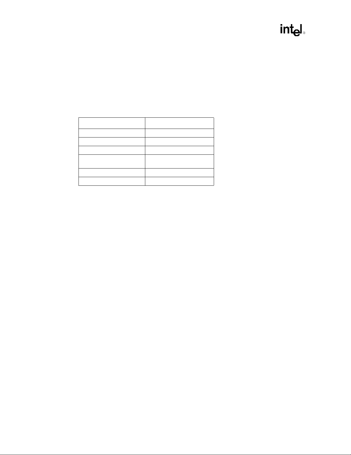
T able 1-1. Reference Documents
®
Xeon™
Document
603-Pin Socket Design Guidelines
82562ET 10/100 Mbps Platform LAN Connect (PLC) Product Datasheet
APIC External Design Specification
AT Attachment - 6 with packet Interface (ATA/ATAPI - 6)
CK-408B Clock Synthesizer/Driver Specification Revision 1.1
ITP700 Debug Port Design Guide
Intel® Xeon™ Processor with 512 KB L2 Cache Signal Integrity Models
Intel® 82801CA I/O Controller Hub 3 (ICH3-S) Datasheet 290733
®
Intel
PCI-64 Hub 2 (P64H2) Thermal and Mechanical Design Guidelines 298648
®
Intel
E7500 Chipset Thermal and Mechanical Design Guidelines 298647
®
Intel
PCI-64 Hub 2 (P64H2) Datasheet 290732
®
Intel
E7500 Chipset Memory Controller Hub (MCH) Datasheet 290730
Design Guide 15
http://developer.intel.com/design/
Xeon/guides/249672.htm
http://developer.intel.com/design/
Xeon/guides/
http://developer.intel.com/design/
Xeon/devtools
Document
Number/Source
Page 16

Introduction
Table 1-1. Reference Documents
Document
http://www.pcisig.com/
PCI Bus Power Management Interface Specification, Revision 1.1
PCI Hot Plug Specification, Revision 1.1
PCI Local Bus Specification, Revision 2.2
PCI-PCI Bridge Architecture Specification, Revision 1.1
PCI Standard Hot-Plug Controller and Subsystem Specification, Revision 1.0
PCI-X Specification, Revision 1.0a
System Management Bus Specification (SMBus), Revision 1.1 http://www.smbus.org/specs/
Universal Serial Bus Specification, Revision 1.1
VRM 9.1 DC-DC Converter Design Guidelines
Intel® Xeon™ Processor Voltage Regulator Down (VRD) Design Guidelines
Intel® Xeon™ Processor with 512 KB L2 Cache System Compatibility
Guidelines
Intel® Xeon™ Processor Thermal Design Guidelines
Intel® Xeon™ Processor Thermal Solution Functional Specifications
Intel® Xeon™ Processor with 512 KB L2 Cache Thermal Models
Intel® Xeon™ Processor with 512 KB L2 Cache Mechanical Model in IGES
Format
Intel® Xeon™ Processor with 512 KB L2 Cache Mechanical Model in ProE*
Format
Intel® Xeon™ Processor with 512 KB L2 Cache at 1.80 GHz, 2 GHz, and
2.20 GHz Datasheet
AP-728 Intel® ICH Family Real Time Clock (RTC) Accuracy and
Considerations Under Test Conditions
specifications/
pci_bus_power_management_int
erface
http://www.pcisig.com/
specifications/pci_hot_plug
http://www.pcisig.com/
specifications/conventional_pci
http://www.pcisig.com/
specifications/
pci_to_pci_bridge_architecture
http://www.pcisig.com/
specifications/pci_hot_plug
http://www.pcisig.com/
specifications/pci_x
http://www.usb.org/developers/
docs.html
http://developer.intel.com/design/
Xeon/guides/
http://developer.intel.com/design/
Xeon/guides/
http://developer.intel.com/design/
Xeon/guides/
http://developer.intel.com/design/
Xeon/guides/298348.ht m
http://developer.intel.com/design/
Xeon/applnots/249673.htm
http://developer.intel.com/design/
Xeon/devtools/
http://developer.intel.com/design/
Xeon/devtools/
http://developer.intel.com/design/
Xeon/devtools/
http://developer.intel.com/design/
Xeon/datashts/298642.htm
http://developer.intel.com/design/
chipsets/applnots/292276.htm
Document
Number/Source
16 Design Guide
Page 17
1.2 Conventions and Terminology
This section defines conventions and terminology used throughout the design guide.
Convention/Terminology Description
Aggressor A network that transmits a coupled signal to another network.
AGTL+ The Xeon™ processor family system bus uses a bus technology called AGTL+,
Asynchronous GTL+ Xeon processors do not utilize CMOS voltage levels on any signals that connect
Bus Agent A component or group of components that, when combined, represent a single
Core Power Core power refers to a power rail that is on only during full-power operation.
Crosstalk The reception on a victim network of a signal imposed by aggressor network(s)
Derived power A derived power rail is any power rail that is generated from another power rail
Dual Processor (DP) Used to specify a system configuration using two processors.
Electromagnetic
Compatibility (EMC)
Electromagnetic
Interference (EMI)
or Assisted Gunning Transceiver Logic. AGTL+ buffers are open-drain, and
require pull-up resistors to provide the high logic level and termination. AGTL+
output buffers differ from GTL+ buffers with the addition of an active pMOS pullup transistor to assist the pull-up resistors during the first clock of a low-to-high
voltage transition.
to the processor. As a result, legacy input signals such as A20M#, IGNNE#,
INIT#, LINT0/INTR, LINT1/NMI, PWRGOOD, SMI#, SLP#, and STPCLK# utilize
GTL+ input buffers. Legacy output signals (FERR# and IERR#) and non-AGTL+
signals (THERMTRIP# and PROCHOT#) also utilize GTL+ output buffers. All of
these signals follow the same DC requirements as AGTL+ signals, however the
outputs are not actively driven high (during a logical 0 to 1 transition) by the
processor (the major difference between GTL+ and AGTL+). These signals do
not have setup or hold time specifications in relation to BCLK[1:0], and are
therefore referred to as “Asynchronous GTL+ Signals”. However, all of the
Asynchronous GTL+ signals are required to be asserted for at least two BCLKs
in order for the processor to recognize them.
load on the AGTL+ bus.
These power rails are on when the active-low PSON signal is asserted to the
power supply. The core power rails that are distributed directly from the power
supply are: +12 V, +5 V, and +3.3 V.
through inductive and capacitive coupling between the networks.
• Backward Crosstalk – Coupling that creates a signal in a victim network that
travels in the opposite direction as the aggressor’s signal.
• Forward Crosstalk – Coupling that creates a signal in a victim network that
travels in the same direction as the aggressor’s signal.
• Even Mode Crosstalk – Coupling from a signal or multiple aggressors when
all the aggressors switch in the same direction that the victim is switching.
• Odd Mode Crosstalk – Coupling from a signal or multiple aggressors when
all the aggressors switch in the opposite direction that the victim is switching.
using an on-board voltage regulator. For example, +2.5 V is derived from a +5 V
power rail using a voltage regulator.
The successful operation of electronic equipment in its intended electromagnetic
environment.
Electromagnetic radiation from an electrical source that interrupts the normal
function of an electronic device.
Introduction
Design Guide 17
Page 18
Introduction
Convention/Terminology Description
Flight Time Flight time is a term in the timing equation that includes the signal propagation
Full-power During full-power operation, all components on the motherboard remain
GTLREF Reference voltage for AGTL+ input pins.
Inter-Symbol
Interference (ISI)
Network The network is the trace of a Printed Circuit Board (PCB) that completes an
Overshoot The maximum voltage observed for a signal at the device pad, measured with
Pad The electrical contact point of a semiconductor die to the package substrate. A
Pin The contact point of a component package to the traces on a substrate, such as
Power-Good “Power-Good,” “PWRGOOD,” or “CPUPWRGOOD” (an active high signal)
Power Rails A power supply has five power rails: +12 V, –12 V, +5 V, +3.3 V, and +5 VSB. In
Ringback The voltage to which a signal changes after reaching its maximum absolute
System Bus The System Bus is the bus which connects the processor to the platform.
Setup Window The time between the beginning of Setup to Clock (TSU_MIN) and the arrival of
delay, any effects the system has on the Tco of the driver, plus any adjustments
to the signal at the receiver needed to guarantee the setup time of the receiver.
More precisely, flight time is defined as:
• The time difference between a signal at the input pin of a receiving agent
crossing the switching voltage (adjusted to meet the receiver manufacturer’s
conditions required for AC timing specifications; i.e., ringback, etc.) and the
output pin of the driving agent crossing the switching voltage when the driver
is driving a test load used to specify the driver’s AC timings.
• Maximum and Minimum Flight Time – Flight time variations are caused by
many different parameters. The more obvious causes include variation of
the board dielectric constant, changes in load condition, crosstalk, power
noise, variation in termination resistance, and differences in I/O buffer
performance as a function of temperature, voltage, and manufacturing
process. Some less obvious causes include effects of Simultaneous
Switching Output (SSO) and packaging effects.
• Maximum flight time is the largest acceptable flight time that a network
experiences under all conditions.
• Minimum flight time is the smallest acceptable flight time that a network
experiences under all conditions.
powered. Note that full-power operation includes both the full-on operating state,
and the S1 (processor stop-grant) state.
The effect of a previous signal (or transition) on the interconnect delay. For
example, when a signal is transmitted down a line, and the reflections due to the
transition have not completely dissipated, the following data transition launched
onto the bus is affected. ISI is dependent upon frequency, time delay of the line,
and the reflection coefficient at the driver and receiver. ISI can impact both timing
and signal integrity.
electrical connection between two or more components.
respect to VCC.
pad is only observable in simulations.
the motherboard. Signal quality and timings can be measured at the pin.
indicates that all of the system power supplies and clocks are stable.
PWRGOOD should go active a predetermined time after system voltages are
stable and should go inactive as soon as any of these voltages fail their
specifications.
addition to these power rails from the power supply, several other power rails are
created by voltage regulators on the Reference Board.
value. Ringback may be caused by reflections, driver oscillations, or other
transmission line phenomena.
a valid clock edge. This window may be different for each type of bus agent in
the system.
18 Design Guide
Page 19

Convention/Terminology Description
Introduction
Simultaneous Switching
Output (SSO)
Standby Power Rail Standby power is supplied by the power supply during times when the system is
Stub The branch from the bus trunk terminating at the pad of an agent.
Trunk The main connection, excluding interconnect branches, from one end agent pad
Undershoot The minimum voltage extending below VSS observed for a signal at the device
VCC_CPU VCC_CPU is the core power for the processor. The system bus is terminated to
Victim A network that receives a coupled crosstalk signal from another network is called
VRM 9.1 “VRM 9.1” refers to the Voltage Regulator Module specification for the Xeon
Effects which are differences in electrical timing parameters and degradation in
signal quality caused by multiple signal outputs simultaneously switching voltage
levels in the opposite direction from a single signal or in the same direction.
These are called odd mode and even mode switching, respectively. This
simultaneous switching of multiple outputs creates higher current swings that
may cause additional propagation delay (“push-out”) or a decrease in
propagation delay (“pull-in”). These SSO effects may impact the setup and/or
hold times and are not always taken into account by simulations. System timing
budgets should include margin for SSO effects.
powered down. The purpose is to maintain functions that always need to be
enabled, such as the date and time-of-day within the BIOS. The power supply
provides a +5 VSB power rail.
to the other end agent pad.
pad.
VCC_CPU.
the victim network.
processor. It is a DC-DC converter module that supplies the required voltage and
current to a single processor.
1.3 System Overview
The E7500 chipset is Intel’s first generation server chipset designed for use with the Xeon
processor. The architecture of the chipset provides the performance and feature-set required for
dual-processor based severs in the entry- level and mid-range, front -end and g eneral-purp ose server
market segments. A new chipset component interconnect, the Hub Interface 2.0 (HI2.0), is
designed into the E7500 chipset to provide more efficient communication between chipset
components for high-speed I/O . Each HI2.0 prov ides 1.066 GB/s I/O bandwidt h. The E7500 MC H
has three HI2.0 connectio ns , d eliv eri ng 3.2 G B /s b andw id th fo r h i gh- sp eed I /O, which can be used
for PCI/PCI-X bridges. The system bus, used to connect the processor with the E7500 chipset,
utilizes a 400 MHz transfer rate for data transfers, delivering 3.2 GB/s. The E7500 chipset
architecture supports a 144-bit wide, 200 MHz DDR memory interface also capable of transferring
data at 3.2 GB/s.
In addition to these performance features, E7500 chipset-based platforms also provide the RASUM
(Reliability, Availability, Serviceability, Usability, and Manageability) features required for entrylevel and mid-range servers. These features include: Chipkill* technology ECC for memory, ECC
for all high-performance I/O, out-of-band manageability through SMBus target interfaces on all
major components, memory scrubbing and auto-initialization, processor thermal monito ring, and
hot-plug PCI. For a complete list of the features on this platform, refer to the component datasheets
listed in Section 1.1.
Design Guide 19
Page 20
Introduction
1.3.1 Intel® Xeon™ Processor with 512 KB L2 Cache
The Intel Xeon processor with 512 KB L2 cache is the second generation of microprocessors
targeted for severs and workstations using the Intel
processor delivers performance levels that are sign ificantly hig her th an previou s g eneratio ns of IA32 processors. The E7500 chipset supports all speeds of the Intel Xeon processor with 512 KB L2
cache.
Table 1-2. Intel
L2 Cache 512 KB
Data Bus Transfer Rate 3.2 GB/s
Multi-Processor Support 1–2 CPUs
Manageability Features
Package 603-pin micro-PGA
Operating Voltage 1.50 V
Unless otherwise noted, the term “processor” refers to the Xeon processor.
The Xeon processor includes the following advanced microarchitecture features:
• Hyper Pipelined Technology.
• Advanced Dynamic Execution.
• Execution Trace Cache.
®
NetBurst™ microarchitecture. The Xeon
®
Xeon™ Processor with 512 KB L2 Cache Feature Set Overview
Feature Xeon™
Intel and OEM EEPROMs and
thermal sensor on package
• Streaming SIMD (single instruction, multiple data) Extensions 2.
• Advanced Transfer Cache.
• Enhanced Floating Point and Multimedia Engine.
The Intel Xeon processor system bus utilizes a split-transaction, deferred reply protocol similar to
that of the Intel
with the Pentium III Xeon processor bus. The system bus uses source-synchronous transfer of
address and data to improve performance and enables addressing at 2X the system bus frequency
of 100 MHz and data transfers at 4X the system bus frequency of 100 MHz. This allows the
processors to transfer data at 3.2 GB/s.
The Xeon processor provides manageability features consistent with Intel
processors. These features include the Processor Information ROM, the OEM EEPROM, and the
processor thermal sensor; all of which are accessed through the System Management Bus
(SMBus). The Processor Information ROM is a 128-byte read-only device that incorporates Intel
processor specific data. The OEM EEPROM, also known as the “scratchpad EEPROM,” is a
128-byte read/write EEPROM in which an OEM may program system specific data. The thermal
sensor monitors the temperature of the processor die.
®
Pentium III Xeon™ processor bus, however the system bus is not compatible
®
Pentium® III Xeon™
20 Design Guide
Page 21

1.3.2 Intel® E7500 Chipset
Introduction
The E7500 chipset consists of three major components: the Intel® E7500 Memory Controller Hub
(referred to throughout this document as the MCH), the Intel
(hereafter referred to as ICH3-S), and th e Intel
P64H2). The chipset components communicate via hub interfaces (HIs). The MCH provides four
hub interface connections: one for the ICH3-S and three for high-speed I/O using 82870P2 P64H2
components. The hub interfaces are point-to-po int and therefore on ly support two agents (the MCH
plus one I/O device). Therefore, the system supports a total of three P64H2s.
®
82870P2 PCI/ PCI-X 64-bit Hub 2 (abbreviated to
1.3.2.1 Intel® E7500 Memory Controller Hub (MCH)
The MCH is a 1005-ball FC-BGA package and contains the following functionality:
• System Bus Features:
— Supports dual processors at 100 MHz (x4 transfers).
— System bus bandwidth of 3.2 GB/s (400 MHz).
— Supports 36-bit system bus addressing model.
— 12 deep in-order queue, 2 deep defer queue.
• Memory Bus Features:
— 144-bit wide, DDR-200 memory interface with memory bandwidth of 3.2 GB/s.
— Supports x72, ECC, registered DDR-200 DIMMs using 64-Mb, 128-Mb, 256-Mb and
512-Mb DRAMs.
— Supports a maximum of 16 GB of memory.
— Supports Single 4-bit Error Correct, Double 4-bit Error Detect (S4EC/D4ED) Chipkill
technology ECC (x4 Chipkill technology).
— Supports up to 32 simultaneous open pages.
®
82801CA I/O Controller Hub 3-S
• I/O Features:
— Provides HI1.5 connection for ICH3-S (Hub Interface A):
- 266 MB/s point-to-point connection for ICH3-S with parity protection.
- 8-bit wide, 66 MHz base clock, 4X data transfer.
- Parallel termination mode for longer trace lengths.
- 64-bit inbound addressing, 32-bit outbound addressing.
— Provides 3 HI2.0 Connections for P64H2s (Hub Interfaces B, C and D):
- 1.066 GB/s point-to-point connection for I/O bridges with ECC protection.
- 16-bit wide, 66 MHz base clock, 8X data transfer.
- Parallel termination mode for longer trace lengths.
- 64-bit inbound addressing, 32-bit outbound addressing.
• Power Management Features:
— Supports C0, C1, C2, S0, S1, S4, and S5 power states. (Does not support C3, C4, S2,
and S3).
Design Guide 21
Page 22

Introduction
1.3.2.2 I/O Controller Hub 3 (Intel® ICH3-S)
The I/O Controller Hub (ICH3-S) provides the legacy I/O subsystem for E7500 chipset-based
platforms. Additionally, it integrates many advanced I/O functions. The ICH3-S includes the
following features:
• Provides HI1.5 Connection to MC H:
— 266 MB/s point-to-point connection for ICH3-S with parity protection.
— 8-bit wide, 66 MHz base clock, 4X data transfer.
— Parallel termination mode for longer trace lengths.
— 64-bit inbound addressing, 32-bit outbound addressing.
• 2 channel Ultra ATA/100 bus master IDE controller.
• 3 Universal Host Controller Interface (UHCI) USB 1.1 compliant host controllers
(Capabilities for six ports).
• I/O APIC.
• System Management Bus (SMBus) Specificatio n, Version 1.1 compliant controller.
• LPC interface.
• AC '97 Component Specification, Revision 2.2 compliant interface.
• PCI Local Bus Specification, Revision 2.2 compliant interface.
• Integrated LAN Controller.
1.3.2.3 PCI/PCI-X 64-bit Hub 2 (Intel® 82870P2 P64H2)
The P64H2 provides PCI/PCI-X, high-performance I/O capability on E7500 chipset based
platforms. Each P64H2 component includes:
• 16-bit, HI2.0 Connection to MCH:
— 1 GB/s point-to-point connection for I/O bridges with ECC protection.
— 16-bit wide, 66 MHz base clock, 8X data transfer.
— Parallel termination mode for longer trace lengths.
— 64-bit inbound addressing, 32-bit outbound addressing.
• Two Independent, 64-bit PCI/PCI-X Interfaces:
— PCI-X Specification, Revision 1.0a compliant.
— PCI Local Bus Specification, Revision 2.2 compliant.
— PCI-PCI Bridge Architecture Specification, Revision 1.1 compliant.
— PCI Hot Plug Specification, Revision 1.1 compliant.
— One PCI Hot Plug Controller (PHPC) per PCI/PCI-X interface.
— One IOxAPIC per PCI/PCI-X Interface (16 external, 8 internal interrupts).
— SMBus target for access to all internal PCI registers.
22 Design Guide
Page 23
1.3.3 Bandwid th Summary
Table 1-3 describes the clock maximum speed, sample rate, and bandwidth for each of the
interfaces in the E7500 chipset based platform.
Table 1-3. Platform Maximum Bandwidth Summary
Introduction
Interface
Clock Speed
(MHz)
Samples per
Clock
Data Width
(Bytes)
System Bus (Data) 100 4 8 3200
DDR Interface 100 2 16 3200
Hub Interface A 66 4 1 266
Hub Interface B, C, D 66 8 2 1066
PCI-X 133 1 8 1066
1.3.4 System Configurations
Figure 1-1 illustrates an example E7500 chipset-based system configuration for server platforms
using Xeon processors.
Figure 1-1. Example Intel® Xeon™ Processor with 512 KB L2 Cache / Intel® E7500 Chipset
Based System Configuration
ProcessorProcessor
System Memory
200 MHz
DDR
200 MHz
DDR
Hot Plug
Hot Plug
Hot Plug
PCI / PCI-X
PCI / PCI-X
PCI / PCI-X
PCI / PCI-X
PCI / PCI-X
PCI / PCI-X
SMBus
Devices
GPIOs
Super I/O
1–4 FWHs
10/100 LAN
Controller
AC '97
Codec(s)
SMBus 1.1
LPC I/F
AC'97 2.1
Intel
ICH3-S
MCH
16-bit
HI 2.0
16-bit
HI 2.0
®
8-bit
HI 1.5
16-bit
HI 2.0
Intel®
P64H2
P64H2
P64H2
Bandwidth
(MB/s)
USB 1.1, 6 Ports
4 IDE Devices
UltraATA/100
PCI Bus
Agent
PCI
PCI
Slots
Design Guide 23
Page 24

Introduction
This page is intentionally left blank.
24 Design Guide
Page 25

Component Quadrant Layout
Component Quadrant Layout 2
The following figures show only general quadrant information, not exact component ball count.
Designers should use only the exact ball assignment to conduct routing analyses. Reference the
following documents for exact ball assignment information.
®
• Intel
• Intel
• Intel
• Intel
Xeon™ Process or wi th 512 KB L2 Cache at 1.80 G Hz, 2 GH z , a nd 2.2 0 G Hz Dat as heet
®
82801CA I/O Controller Hub 3 (ICH3-S) Datasheet
®
PCI-64 Hub 2 (P64H2) Datasheet
®
E7500 Chipset Memory Controller Hub (MCH) Datasheet
Design Guide 25
Page 26
Component Quadrant Layout
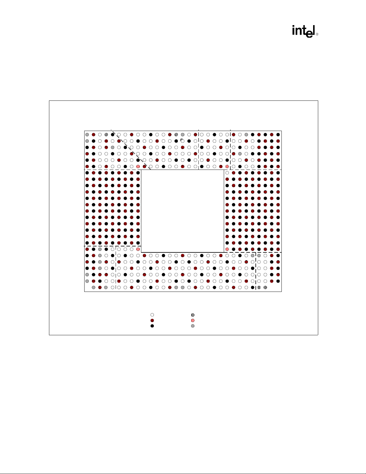
2.1 Intel® Xeon™ Processor with 512 KB L2 Cache Quadrant Layout
Figure 2-1. Intel® Xeon™ Processor with 512 KB L2 Cache Quadrant Layout (Top View)
COMMON
CLOCK
A
B
C
D
E
F
G
H
J
K
L
M
N
Vcc/Vss
P
R
T
U
V
W
Y
AA
AB
AC
AD
AE
ADDRESS
3 5 7 9 11 13 15 17 19 21 23 25 27 29 311
2 4 6 8 10 12 14 16 18 20 22 24 26 28
CLOCKS SMBus
DATA
COMMON
CLOCK
Async /
JTAG
A
B
C
D
E
F
G
H
J
K
L
M
N
P
R
T
U
V
W
Y
AA
AB
AC
AD
AE
Vcc/Vss
= Signal
= Power
= Ground = Reserved/NC
= SM_VCC
= GTLREF
26 Design Guide
Page 27
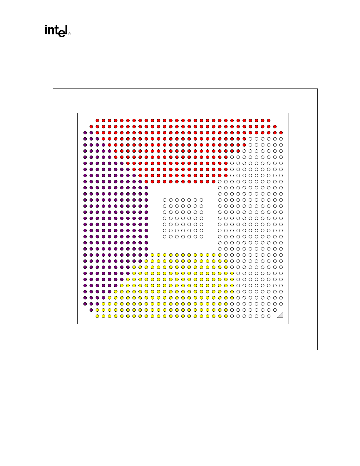
2.2 Intel® E7500 MCH Quadrant Layout
Figure 2-2. Intel® E7500 MCH Quadrant Layout (Top View)
DDR A
333231302928272625242322212019181716151413121110987654321
Component Quadrant Layout
AN
AM
AL
AK
AJ
AH
AG
AF
AE
AD
AC
AB
AA
Y
W
V
DDR B
U
T
R
P
N
M
L
K
J
H
G
F
E
D
C
B
A
AN
AM
AL
AK
AJ
AH
AG
AF
AE
AD
AC
AB
AA
Y
W
V
U
T
R
P
N
M
L
K
J
H
G
F
E
D
C
B
A
Bus
System
333231302928272625242322212019181716151413121110987654321
HI_A–D
Design Guide 27
Page 28

Component Quadrant Layout
2.3 Intel® ICH3-S Quadrant Layout
Figure 2-3. Intel® ICH3-S Quadrant Layout (Top View)
PCI
LPC
GPIO
LAN
2
1
A
B
C
D
E
F
G
H
J
K
L
M
N
P
R
T
U
V
O
OOO
W
O
O
Y
O
O
O
AA
AB
AC
O
2
1
O
3
6
54
SMBus
1110
987
15
IDE
O
19
181716141312
222120191817161514131211109876543
OOO
O
O
O
O
21
22
20
23
O
O
O
O
23
A
B
C
D
E
F
G
H
J
K
L
M
N
Interface
P
R
T
U
V
W
Y
AA
AB
AC
USB
HUB
CPU
LPC/Firm Ware
LAN
AC'97
EEPROM
VSS
VCC_1.8
VCCSUS_1.8
CLK
IDE
HUB Interface
NC VCC_3.3 USB
GPIO VCCSUS_3.3 CPU
O
RTC SMBusMisc. VCC
28 Design Guide
Page 29
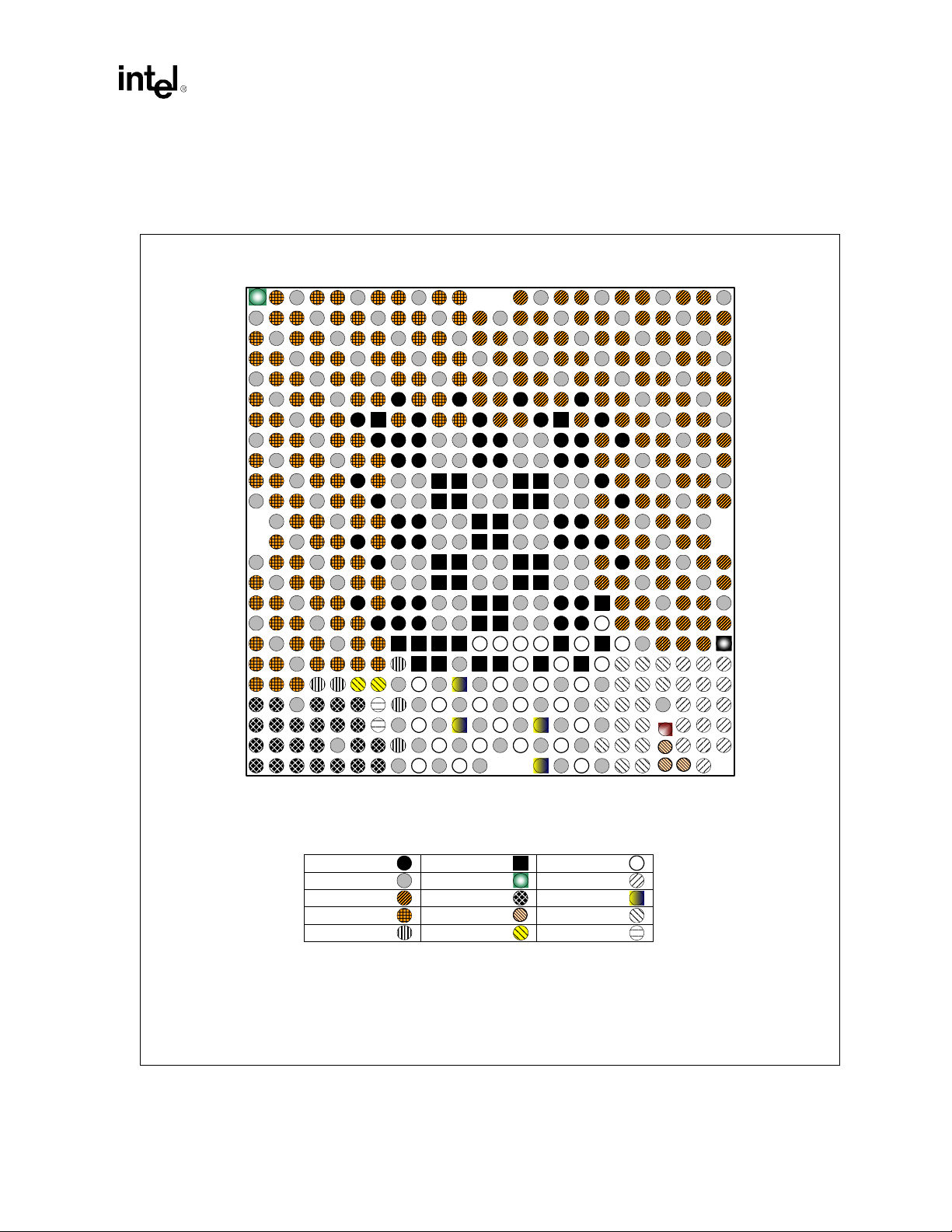
Component Quadrant Layout
2.4 Intel® 82870P2 P64H2 Quadrant Layout
Figure 2-4. Intel® P64H2 Quadrant Layout (Top View)
24 2223 21 20 19 18 17 16 15 14 13 12 11 10 9 8 7 6 5 4 3 2 1
AD
AC
AB
AA
Y
W
V
U
T
R
PCI / PCI-X Channel A
P
N
M
L
K
J
H
G
F
E
D
C
B
A
24 2223 21 20 19 18 17 16 14 13 12 11 10 9 8 7 6 5 4 3 2 1
15
O
AD
AC
PCI / PCI-X Channel B
AB
AA
Y
W
V
U
T
R
P
N
M
L
K
J
H
G
F
E
D
C
B
A
Hot Plug
VCC3.3
VSS
PB
VCC1.8
VCC5REF
HP
HI
PBIRQ
PSTRB
IRQsHub Interface
PA APIC PAIRQ
MISC BPCLK SCLK/SDATA
Design Guide 29
Page 30

Component Quadrant Layout
This page is intentionally left blank.
30 Design Guide
Page 31

Platform Stack-Up and Component Placement Overview
Platform Stack-Up and Component
Placement Overview 3
3.1 Platform Component Placement
Figure 3-1 illustrates the component placement for the Intel Xeon processor with 512 KB L2
cache/Intel E7500 chipset-based customer reference board (E7500 CRB). Table 3-1 lists the
assumptions used for the component placement. Refer to www.ssiforum.org for detailed
information on the SSI (Server System Infrastructure) specification.
T a ble 3-1. Assumptions for System Placement Example
System
Configuration
DP Server Midrange Electronic-Bay (13”x16”) 8 Layers Double Sided
Form Factor (SSI Specification) Number of PCB Layers Assembly
Assumptions
Design Guide 31
Page 32

Platform Stack-Up and Component Placement Overview
3.2 Platform Stack-Up
Figure 3-1. Intel
®
E7500 Chipset Customer Reference Board System Placement Example
Figure 3-2 shows the recommended platform stack-up. All layers are 1 oz copper. The processor
requires 2 oz of copper to deliver power and 2 oz of copper to deliver ground. Vias are 10 mil
finished hole with 35 mil anti-pads and 24 mil pads.
Route signal layers as asymmetric st ripline on layers 2 , 4, 5 an d 7. T he sign al layers must ref erence
ground on layer 3 or layer 6 only. Route signals on layers 4 and 5 orthogonally to reduce crosstalk
between the layers.
Intel strongly recommends that system designers use the stack-up shown in Figure 3-2 and
recommendations in Table 3-2 when designing their boards. Intel realizes numerous ways exist to
achieve these targeted impedance tolerances; contact your board vendor for these specifics. Intel
encourages platform designers to perform comprehensive simulation analysis to ensure all timing
specifications are met. This is particularly important if a design deviates from the design guidelines
provided.
32 Design Guide
Page 33

Platform Stack-Up and Component Placement Overview
Figure 3-2. 8 Layer, 50 Ω Board with 5 mil Traces
Layer 1
Dielectric 9.6 mil
Layer 2
Core 5.2 mil
Layer 3
Dielectric 4.3 mil
Layer 4
Core 14.0 mil
Layer 5
Dielectric 4.3 mil
Layer 6
Core 5.2 mil
Layer 7
Dielectric 9.6 mil
Layer 8
Power
Dielectric
SignalSignal Signal
Core
Ground
Dielectric
SignalSignal Signal
Main Core
SignalSignal Signal
Dielectric
Ground
Core
SignalSignal Signal
Dielectric
Power
T able 3-2. E7500 Chipset Customer Reference Board Requirements
2.1 mil (1 oz + plating)
1.4 mil (1 oz)
1.4 mil (1 oz)
1.4 mil (1 oz)
1.4 mil (1 oz)
1.4 mil (1 oz)
1.4 mil (1 oz)
2.1 mil (1 oz + plating)
Board Factor Recommendation
Material • Standard FR4 Tg 170 Epoxy.
Ω impedance ±10% Layers 2,4,5,7 (except lower left corner SCSI interface).
Impedance
Requirements
Etch
Finished Via Size
• 50
• SCSI interface 83
Ω single ended, 122 Ω differential pair ± 10% (layers 1 and 8
lower left corner).
• 5 mil trace width and space minimum inner/outer.
• SCSI interface; 6 mil separation within a pair, 20 mil space between adjacent pairs.
• Minimum via size is 0.014 mil finished in a 0.026 mil land with 0.040 mil antipad.
• Approximately 15,000 plated through holes total.
Finish • Solder Mask On Bare Copper (SMOBC)
Soldermask Type • SM-840 minimum web 0.004 mils.
Fabrication • Edge Routed.
Component
Technology
• Through hole / SMT.
• QFP, BGA, Front side.
• Discrete 0603, 0805 Back side.
Design Guide 33
Page 34

Platform Stack-Up and Component Placement Overview
This page is intentionally left blank.
34 Design Guide
Page 35

Platform Clock Routing Guidelines
Platform Clock Routing Guidelines 4
To minimize jitter, improve routing, and reduce cost, E7500 chipset-based systems should use a
single chip clock solut ion, the CK 408B. In t his configu ration, t he CK408B provides f our , 1 00 MHz
differential outputs pairs for all of the bus agents, including the ITP connector, and five, 66 MHz
speed clocks that drive all I/O buses. Figure 4-1 shows the implementation of the bus clocks for
this configuration.
For more information on CK408B compliance, refer to the CK408B Clock Synthesizer
Specification Specifically for E7500 Chipset DP with ITP System Clock Generator Document.
Table 4-1. CK408B Clock Groups
Clock Group
Name
Host_CLK 100 Processor 0, Processor 1, Debug Port and MCH
CLK66 66 MCH, ICH3-S, and P64H2
CLK33_ICH3-S 33 ICH3-S
CLK14 14.318 ICH3-S and SIO
CLK33 33 P CI Connec tor, SIO, BMC, and FWH
USBCLK 48 ICH3-S
Frequency
(MHz)
Receiver
Design Guide 35
Page 36

Platform Clock Routing Guidelines
T a ble 4-2. Platform System Clock-Reference
Clock Group CK-408B Pin Component Component Pin Name
Host_CLK CPU# Debug Port BCLK[0]
CPU Debug Port BCLK[1]
CPU# Processor 0 BCLK[0]
CPU Processor 0 BCLK[1]
CPU# Processor 1 BCLK[0]
CPU Processor 1 BCLK[1]
CPU# MCH HCLKINP
CPU MCH HCLKINN
CLK66 66BUF MCH 66IN
CLK33_ICH3-S PCIF ICH3-S PCICLK
CLK14 REF0 ICH3-S CLK14
CLK33 PC I PCI Connector #1 CLK
PCIF BMC LCLK
USBCLK USB-48MHZ ICH3-S CLK48
ICH3-S CLK66
P64H2 CLK66
SIO CLOCKl
PCI Connector #2 CLK
PCI Connector #3 CLK
PCI Connector #4 CLK
PCI Connector #5 CLK
FWH CLK
SIO PCI_CLK
36 Design Guide
Page 37

Platform Clock Routing Guidelines
Figure 4-1. Intel® E7500 Chipset-Based System Clocking Diagram
CK408B
CPU / CPU# (4)
66BUF (5)
REF0 (1)
USB-48MHz (1)
PCIF (3)
PCI (7)
Host_CLK
CLK66
CLK14
USBCLK
CLK33_ICH3-S
CLK33 x7
CLK66
x3
Processor
Processor
ITP
MCH
Intel® ICH-S
CLK33 (x5)
DDR
Channel A
DIMMclk (x4 pr.)
DDR
Channel B
DIMMclk (x4 pr.)
P
P
P
P
C
C
C
C
I
32 bit
I
I
I
33MHz
D
D
I
D
I
D
M
I
M
I
M
M
M
M
M
M
D
D
I
D
I
D
M
I
M
I
M
M
M
M
M
M
Super I/O
FWH
BMC
Intel® P64H2
PCIclk
x7
P
P
P
P
C
C
C
C
I
I
I
I
Design Guide 37
PCIclkx7PCIclk
P
P
P
P
C
C
C
C
I
I
I
I
P64H2 P64H2
x7
P
P
P
P
C
C
C
C
I
I
I
I
PCIclkx7PCIclk
P
P
P
P
C
C
C
C
I
I
I
I
P
P
C
C
I
P
P
C
C
I
I
I
PCIclk
x7
x7
P
P
P
P
C
C
C
C
I
I
I
I
Page 38

Platform Clock Routing Guidelines
4.1 Clock Groups
4.1.1 HOST_CLK Clock Group
4.1.1.1 HOST_CLK Clock Topology
The clock synthesizer provides four sets of 100 MHz differential clock outputs. The 100 MHz
differential clocks are driven to the Processors, the MCH, and the processors’ debug port as shown
in Figure 4-1.
The clock driver differential bus output structure is a “Current Mode Current Steering” output
which develops a clock signal by alternately steering a programmable constant current to the
external termination resistors “Rt.” The resulting amplitude is determined by multiplying IOUT by
the value of Rt. The current IOUT is programmable by a resistor and an internal multiplication
factor so the amplitude of the clock signal can be adjusted for different values of “R”’ to match
impedances or to accommodate future load requirements.
The recommended termination for the differential bus clock is a “Shunt Source Termination.”
Refer to Figure 4-2 for an illustration of this termination scheme. Parallel Rt resistors perform a
dual function, converting the current output of the clock driver to a voltage and matchi ng the driver
output impedance to the transmission line. The series resistors “Rs” provide isolation from the
clock driver's output parasitics, which would otherwise appear in parallel with the termination
resistor Rt.
The value of Rt should be selected to match the characteristic impedance of the motherboard, and
Rs should be between 20 Ω and 33 Ω. Simulations have shown that Rs values above 33 Ω provide
no benefit to signal integrity but only degrade the edge rate.
• Mult0 pin (pin #43) is pulled high – making the multiplication factor 6.
• Iref pin (pin # 42) is connected to ground through a 475 Ω ± 1% resistor – making the Iref
2.32 mA.
Figure 4-2. Source Shunt Termination
L1
L1'
Clock
Driver
LT = L1 + L2 + L4
Rs
Rs
L2
L2'
L3 L3'
Rt Rt
L4
L4'
Processor or
MCH
38 Design Guide
Page 39

Table 4-3. HOST_CLK[1:0]# Routing Guidelines
Layout Guideline Value Illustration Notes
HOST_CLK Skew between Agents
Trace Width 5 mils Figure 4-4
Differential Pair Spacing 20 – 25 mils Figure 4-4 5,6
Spacing to Other Traces 25 mils Figure 4-4
Serpentine Spacing
Motherboard Impedance – Differential 100
Motherboard Impedance – Single Ended 50
Processor Routing Length –
L1, L1’: Clock Driver to Rs
Processor Routing Length –
L2, L2’: Rs to Rs-Rt Node
Processor Routing Length –
L3, L3’: Rs-Rt Node to Rt
Processor Routing Length –
L4, L4’: Rs-Rt Node to Load
MCH Routing Length –
L1, L1’: Clock Driver to Rs
MCH Routing Length –
L2, L2’: Rs to Rs-Rt Node
MCH Routing Length –
L3, L3’: Rs-Rt Node to Rt
MCH Routing Length –
L4, L4’: Rs-Rt Node to Load
Processor to MCH Length Matching (LT)
Processor to Processor Length Matching (LT)
HOST_CLK0 – HOST_CLK1 Length Matching ± 10 mils
Rs Series Termination Value 20 – 33
Rt Shunt Termination Value
Platform Clock Routing Guidelines
300 ps total budget:
150 ps for clock driver
150 ps for interconnect
Maintain a minimum S/ h rat i o
of > 5/26
Keep parallel serpentine
sections as short as possible.
Minimize 90 degree bends.
Make 45 degree bends, if
possible.
Ω typical 8
Ω ± 10% 9
0 – 0.5” Figure 4-2 13
0 – 0.2” Figure 4-2 13
0 – 0.2” Figure 4-2 13
0 – 22” Figure 4-2
0 – 0.5” Figure 4-2 13
0 – 0.2” Figure 4-2 13
0 – 0.2” Figure 4-2 13
0 – 22” Figure 4-2
0.035” ± 0.010”
MCH LT must be 0.076”
longer than Processor LT.
± 10 mils Figure 4-2 15
Ω ± 5% Figure 4-2 11
Ω ± 1%
49.9
(for 50
Ω board impedance)
Figure 4-2
and
Figure 4-3
Figure 4-4
Figure 4-2 10
Figure 4-2 12
1,2,3,4
NOTES:
1. The skew budget includes clock driver output pair to output pair jitter (differential jitter) and skew, clock skew
due to interconnect process variation, and static skew due to layout differences between clocks to all bus
agents.
2. This number does not include clock driver common mode (cycle to cycle) jitter or spread spectrum clocking.
3. The interconnect portion of the total budget for this specification assumes clock pairs are routed on multiple
routing layers and routed no longer than the maximum recommended lengths.
Design Guide 39
Page 40

Platform Clock Routing Guidelines
4. Skew measured at the load between any two-bus agents. Measured at the crossing point.
5. Edge to edge spacing between the two traces of any differential pair. Uniform spacing should be maintained
along the entire length of the trace.
6. Clock traces are routed in a differential configuration. Maintain the minimum recommended spacing between
the two traces of the pair. Do not exceed the maximum trace spacing because this degrades the noise
rejection of the network.
7. Set line width to meet correct motherboard impedance. The line width value provided here is a
recommendation to meet the proper trace impedance based on the recommended stack up.
8. The differential impedance of each clock pair is approximately 2*Zsingle-ended*(1-2*Kb) where Kb is the
backwards cross-talk coefficient. For the recommended trace spacing, Kb is very small, and the effective
differential impedance is approximately equal to 2 times the single-ended impedance of each half of the pair.
9. The single ended impedance of both halves of a differential pair should be targeted to be of equal value. They
should have the same physical construction. If the HOST_CLK traces vary within the tolerances specified,
both traces of a differential pair must vary equally.
10.L ength compensation for the processor socket and package delay is added to chipset routing to match
electrical lengths between the chipset and the processor from the die pad of each. Therefore, the
motherboard trace length for the chipset will be longer than that for the processor.
11.Rs values between 20
12.Rt shunt termination value should match the motherboard impedance.
13.Minimize L1, L2 and L3 lengths. Long lengths on L2 and L3 degrade effectiveness of source termination and
contribute to ringback.
14.The goal of constraining all bus clocks to one physical routing layer is to minimize the impact on skew due to
variations in Er and the impedance variations due to physical tolerances of circuit board material.
15.Length of LT for one processor must match the LT of all other HOST_CLK traces to other processor with
specified tolerance.
Ω and 33 Ω have been shown to be effective.
Figure 4-3. Clock Skew As Measured from Agent to Agent
BCLK at
Processor
BCLK
at CS
Figure 4-4. Trace Spacing for HOST_CLK Clocks
W
BCLK0 BCLK1
h
Ground Plane
BCLK Slew
W
S
S1S1
40 Design Guide
Page 41

4.1.1.2 HOST_CLK General Routing Guidelines
When routing the 100 MHz differential clocks, do not split up the two halves of a differential
•
clock pair between layers. Route to all agents on the s ame p hysical rou t ing lay er ref erenced to
ground.
• If a layer transition is required, make sure skew induced by the vias used to transition between
routing layers is compensated in the traces to other agents.
• Do not place vias between adjacent complementary clock traces, and avoid differential vias.
Vias placed in one half of a differential pair must be matched by a via in the other half.
Differential vias can be placed within length L1, between clock driver and Rs, if needed to
shorten length L1.
4.1.1.3 CK408 vs. CK408B Requirement
The CK408 and CK408B are pin compatible. The only difference between the two chips is the
CK408B replaces two signals on the CK408 with a fourth HOST_CLK pair for the
In_Target_Probe (ITP) and is preferred by board designers for preliminary testing and validation.
While the CK408B pins need to be connected to the ITP, the CK408 pins require the following
stuffing options:
• Add one 10 kΩ ± 5% pull-up resistor close to the clock driver before the 33 Ω ± 5% (Rs)
(see Figure 4-5) series resistor on each ITP signal trace (CPU3, CPU3#). This would give the
option to use the CK408 instead of the CK408B.
Platform Clock Routing Guidelines
• If deciding to go with CK408, having the 33 Ω ± 5% series resistor and 49.9 Ω ± 1% (Rt)
(see
Figure 4-5) parallel resistor is not necessary.
Figure 4-5. Stuffing Options for CK408 and CK408B
VCC3_3
CK408x
CPU3 / S0
VCC3_3
CPU3# /
CPU_STOP#
CK408: 10 kΩ ± 5%
CK408B: no pop
To ITP BCLK1
CK408: no pop
CK408B: Rs
CK408: 10 kΩ ± 5%
CK408B: no pop
To ITP BCLK1
CK408: no pop
CK408B: Rs
Design Guide 41
Page 42

Platform Clock Routing Guidelines
4.1.2 CLK66 Clock Group
In the CLK66 clock group, the driver is the clock synthesizer 66 MHz clock output buffer, and the
receiver is the 66 MHz clock input buffer at the MCH, ICH3-S, and P64H2.
Figure 4-6. Topology for CLK66
Clock
Driver
Table 4-4. CLK66 Routing Guidelines
Parameters Routing Guide lines
Clock Group CLK66
Topology Point-to-Point
Reference Plane Ground referenced (contiguous over entire length)
Characteristic Trace Impedance (Z
Trace Width 5 mils
Trace Spacing 25 mils
Trace Length – L1 0.00” – 0.50”
Trace Length – L2 3.00” – 9.0”
Resistor R1 = 43
Skew Requirements
Clock Driver to MCH X = (3” – 9.5”)
Clock Driver to ICH3-S X = (3” – 9.5”)
Clock Driver to P64H2 X – 0.34”
L1 L2
R1
) 50 Ω ± 10%
0
Ω ± 5%
All the clocks in the CLK66 group must have < 100 mil skew
between each other.
1
2
Intel
Intel
MCH,
®
ICH3-S,
®
P64H2
NOTES:
1. For better understanding of the concept, refer to Section 4.1.2.1, Figure 4-7 and Figure 4-8.
2. Assuming no connector.
42 Design Guide
Page 43

4.1.2.1 CLK66 Skew Requireme nts
Traces going to the P64H2 could ha ve up to two connectors. Designers should keep in mind that all
T otal Lengths are ref erenced to the MC H length (“X”) and as sume no con nector. Each connector is
equivalent to 0.60 inches of trace. Adding a single connector on the P64H2 trace would reduce the
motherboard trace length by the card length “Z” to X – 0.34” – 0.60” – Z = X – 0.94” – Z (refer
to Figure 4-8). In addition, some OEMs migh t co ns ider having the components o n a ri s er, in which
case the riser card trace length designator “Y” should also be accounted for as yet another factor. In
this case the last equation would become X – 0.34” – 0.60”– Z – 0.60”– Y = X – 1.54”–Y – Z
(refer to Figure 4-9). Note that if a riser is used, the motherboard clock trace must be designed for
the specific riser card trace length and connector.
Figure 4-7. Clock Skew Requirements
43 Ω
CK408B
Platform Clock Routing Guidelines
Total Length = X
MCH
Total Length = X - 0.34"
43 Ω
Resistor must be within
500 mils of CK408B
NOTES:
1. All lengths must be matched within 100 mils of target length.
2. 66 MHz clock lines routed with 25 mils isolation from any other signal.
3. Length from CK408B to MCH must be between 3” and 9.5”.
®
Intel
P64H2
Design Guide 43
Page 44

Platform Clock Routing Guidelines
Figure 4-8. Example of Adding a Single Connector
Total Length = X
43 Ω
CK408B
Motherboard Trace Length
= X - 0.34" - 0.60" - Z
= X - 0.94" - Z
43 Ω
Resistor must be within
500 mils of CK408B
NOTES:
1. All lengths must be matched within 100 mils of target length.
2. 66 MHz clock lines routed with 25 mils isolation from any other signal.
3. Length from CK408B to MCH must be between 3” and 9.5”.
4. Each connector is equivalent to ~ 0.60” of trace.
5. Z is the card trace length.
Figure 4-9. Example of Adding Two Connectors and/or a Riser
Total Length = X
CK408B
43 Ω
MCH
®
Intel
P64H2
Z
MCH
Motherboard Trace Length
= X - 0.34" - 0.60" - Z - 0.60" - Y
= X - 1.54" - Z - Y
Intel
®
P64H2
43 Ω
Resistor must be within 500
mils of CK408B
NOTES:
1. All lengths must be matched within 100 mils of target length.
2. 66 MHz clock lines routed with 25 mils isolation from any other signal.
3. Length from CK408B to MCH must be between 3” and 9.5”.
4. Each connector is equivalent to ~ 0.60" of trace.
5. Each riser is equivalent to ~0.60 + Y where Y is the riser card trace length.
6. The riser must be built with the CLK66 trace length matched to the motherboard routed length.
44 Design Guide
Connector
YZ
Page 45

4.1.3 CLK33_ICH3-S Clock
In the CLK33_ICH3-S case, the driver is the clock synthesizer 3 3 MHz clock output buf fer , and the
receiver is the 33 MHz clock input buffer at the ICH3-S.
Figure 4-10. Topology for CLK33_ICH3-S
L1 L2
Platform Clock Routing Guidelines
Clock
Driver
T a ble 4-5. CLK33_ICH3-S Routing Guidelines
Parameter Routing Guidelines
Clock Group CLK33_ICH3-S
Topology Point-to-Point
Reference Plane Ground referenced (contiguous over entire length)
Characteristic Trace Impedance (Z
Trace Width 5 mils
Trace Spacing 25 mils
Trace Length – L1 0.00” – 0.50”
Trace Length – L2 3.00” – 9.0”
Resistor R1 = 33
Skew Requirements Must be matched to ± 100 mils of CLK66
) 50 Ω ± 10%
0
R1
Intel® ICH3-S
Ω ± 5%
Design Guide 45
Page 46

Platform Clock Routing Guidelines
4.1.4 CLK33 Clock Group
For the CLK33 clock group, th e driver is the clo ck synthesi zer 33 MHz clock output buffer, and the
receiver is the 33 MHz clock input buffer at the PCI devices on the PCI cards.
Figure 4-11. Topology for CLK33 to PCI Device Down
L1 L2
Clock
Driver
.
Table 4-6. CLK33 Routing Guidelines for PCI Device Down
Parameter Ro uting Guidelines
Clock Group CLK33
Topology Point-to-Point
Reference Plane Ground referenced (cont iguous over entire length)
R1
Characteristic Trace Impedance (Z
Trace Width 5 mils
Trace Spacing 25 mils
Trace Length – L1 0.00” – 0.50”
Trace Length – L2 3.00” – 9.0”
Resistor R1 = 33
Skew Requirements PCI device – PCI device skew max allowed by
) 50 Ω ± 10%
0
Specification, Rev 2.2
CLK33 signals within ± 1 ns.
PCI Device,
FWH, BMC, SIO
Ω ± 5%
PCI Local Bus
is 2 ns. Therefore, length match with other
46 Design Guide
Page 47

Figure 4-12. Topology for CLK33 to PCI Slot
Platform Clock Routing Guidelines
L1 L2
Clock
Driver
R1
T a ble 4-7. CLK33 Routing Guidelines for PCI Slot
Parameter Routing Guidelines
Clock Group CLK33
Topology Point-to-Point
Reference Plane Ground referenced (contiguous over entire length)
Characteristic Trace Impedance (Z
Trace Width 5 mils
Trace Spacing 10 mils
Trace Length – L1 0.00” – 0.50”
Trace Length – L2 3.00” – 9.0”
Trace Length – C Routed 2.50” per
Resistor R1 = 33 Ω ± 5%
Skew Requirements PCI device – PCI device skew max allowed by
Maximum Via Count Per Signal 1
) 50 Ω ± 10%
0
Specification, Rev 2.2
CLK33 signals within ± 1 ns.
C
Trace On
PCI
Connector
PCI Card
PCI Device
PCI Local Bus Specification, Rev 2.2
PCI Local Bus
is 2 ns. Therefore, length match with other
Design Guide 47
Page 48

Platform Clock Routing Guidelines
4.1.5 CLK14 Clock Group
The driver in the CLK14 clock group is the clock synth esizer 1 4.318 MHz clock ou tput bu ff er, and
the receiver is the 14.318 MHz clock input buffer at the ICH3-S, SIO and LPC.
Figure 4-13. Topology for CLK14
L1 L2
Clock
Driver
Table 4-8. CLK14 Routing Guidelines
Parameter Ro uting Guidelines
Clock Group CLK14
Topology Point-to-Point
Reference Plane Ground referenced (cont iguous over entire length)
Characteristic Trace Impedance (Z
Trace Width 5 mils
Trace Spacing 10 mils
Trace Length – L1 0.00” – 0.50”
Trace Length – L2 3.00” – 9.0”
Resistor R1 = 22
Skew Requirements None
) 50 Ω ± 10%
0
R1
Intel® ICH3-S
SIO, and LPC
Ω ± 5%
48 Design Guide
Page 49

4.1.6 USBCLK Clock Group
For the USBCLK clock group, the d river is t he clock sy nt hes izer U SB cl ock out pu t buffer, and the
receiver is the USB clock input buffer at the ICH3-S. Note that this clock is asynchronous to any
other clock on the board.
Figure 4-14. Topology for USB_CLK
L1 L2
Platform Clock Routing Guidelines
Clock
Driver
T able 4-9. USBCLK Routing Guidelines
Parameter Routing Guideline
Clock Group USBCLK
Topology Point-to-Point
Reference Plane Ground referenced (contiguous over entire length)
Characteristic Trace Impedance (Z
Trace Width 5 mils
Trace Spacing 25 mils
Trace Length – L1 0.00” – 0.50”
Trace Length – L2 3.00” – 12.00”
Resistor R1 = 33
Skew Requirements None – USBCLK is asynchronous to any other clock on the board
Maximum Via Count 2
0
R1
Intel® ICH3-S
) 50 Ω ± 10%
Ω ± 5%
Design Guide 49
Page 50

Platform Clock Routing Guidelines
4.2 Clock Driver Decoupling
The decoupling requirements for a CK408B compliant clock synthesizer are as follows:
• One, 22 µF polarized (decoupling) capacitor placed close to the VDD generation circuitry.
• Eleven, 0.1 µF high-frequency decoupling capacitors placed close to the VDD pins on the
clock drive r.
• Three, 0.1 µF high-frequency decoupling capacitors placed close to the VDDA pins on the
clock drive r.
• One, 10 µF polarized (decoupling) capacitor placed close to the VDDA pins on the clock
driver.
• One, 0.1 µF high-frequency decoupling capacitor placed close to the VDDA generation
circuitry.
• All decoupling capacitors should be placed close to the clock driver pins. Refer to Figure 4-15.
Figure 4-15. Decoupling Capacitors Placement and Connectivity
Ground vias
Ground vias
Ground vias
Ground vias
Ground vias
VSS pins goes through vias on the ground flood to ground plane
VSS
VSS
VSS
VSS
VDDA
FB4
Place the caps as close
aspossible to the pins
VDD
VDD
VDD
VDD
VSS
VDD
XTAL_IN
XTAL-OUT
VSS
PCIF0
PCIF1
PCIF2
VDD
VSS
PCI0
PCI1
PCI2
PCI3
VDD
VSS
PCI4
PCI5
PCI6
VDD
VSS
66BUFF0/
3V66_2
66BUFF/-
3V66_3
66BUFF2/
3V66_4
66IN/3V66_5
PWRDWN_N
VDDA
VSSA
VTT_PWRGD_
N
Pin 1
Pin 2
Pin 3
Pin 4
Pin 5
Pin 6
Pin 7
Pin 8
Pin 9
Pin 10
Pin 11
Pin 12
Pin 13
Pin 14
Pin 15
Pin 16
Ground Flood
Pin 17
Pin 18
Pin 19
Pin 20
Pin 21
Pin 22
Pin 23
Pin 24
Pin 25
Pin 26
Pin 27
Pin 28
VSS
CK408B
Pin 56
Pin 55
Pin 54
Pin 53
Pin 52
Pin 51
Pin 50
Pin 49
Pin 48
Pin 47
Pin 46
Pin 45
Pin 44
Pin 43
Pin 42
Pin 41
Pin 40
Pin 39
Pin 38
Pin 37
Pin 36
Pin 35
Pin 34
Pin 33
Pin 32
Pin 31
Pin 30
Pin 29
Power vias
REF0
S1
CPU3
CPU/3
CPU0
CPU/0
VDD
CPU1
CPU/1
VSS
VDD
CPU2
CPU/2
MULT0
IREF
VSS-IREF
S2
USB 48MHz
DOT 48MHz
VDD-48MHz
VSS-48MHz
3V66_1/VCH
PCI_STOP_N
3V66_0
VDD
VSS
SCLK
SDATA
VDD
VDD
VDD
VSS
FB4
VSS
VSS
VSS
Ground vias
Ground vias
VDDA
Ground vias
Ground vias
50 Design Guide
Page 51

4.3 Clock Driver Power Delivery
Designers must take special care to provide a quiet VDDA supply to the Ref VDD, VDDA and the
48 MHz VDD. These VDDA signals are especially sensitive to switching noise induced by the
other VDDs on the clock chip. They are also sensitive to switching noise generated elsewhere in
the system such as the processor voltage regu lator . It is recomme nded that a ground flood be placed
directly under the clock chip to provide a low impedance connection for the VSS pins. I n addition,
power vias should be distributed evenly throughout the ground flood.
Note: For all power connections to planes, decoupling capacitors, and vias, the maximum trace width
allowable and shortest possible lengths should be used to ensure lowest possible inductance.
4.4 EMI Constraints
Clocks are a significant contributor to EMI. The following recommendations can aid in EMI
reduction:
• Maintain uniform spacing between the two halves of differential clocks.
• Route clocks on physical layer adjacent to the VSS reference plane only.
• Turn off all unused clocks.
Platform Clock Routing Guidelines
Design Guide 51
Page 52

Platform Clock Routing Guidelines
This page is intentionally left blank.
52 Design Guide
Page 53

System Bus Routing Guidelines
System Bus Routing Guidelines 5
This section covers the system bus source synchronous (data, address, and associated strobes) and
common clock signal routing. Table 5-1 li sts the signals and their corresponding signal types.
Table 5-1. System Bus Signal Groups
Signal Group Type Signals
1,2
BPRI#, BR[3:1]#
AGTL+ Common Clock Input Synchronous to BCLK
AGTL+ Common Clock I/O Synchronous to BCLK
AGTL+ Source Synchronous I/O: 4X
Group
AGTL+ Source Synchronous I/O: 2X
Group
AGTL+ Strobes Synchronous to BCLK [1:0]
Async GTL+ Input
Async GTL+ Output
System Bus Clock Clock BCLK0, BCLK1
TAP Input
TAP Output
SMBus Interface
Power/Other Power/Other
1
1
6
6
1
Synchronous to assoc. strobe D[63:0]#, DBI[3:0]#
Synchronous to assoc. strobe A[35:3]#
Asynchronous
Asynchronous
Synchronous to TCK TCK, TDI, TMS, TRST#
Synchronous to TCK TDO
Synchronous to SM_CLK
RESET#
TRDY#
ADS#, AP[1:0]#, BINIT#
BPM[5:0]#
DP[3:0]#, DRDY#, HIT#
LOCK#, MCERR#
ADSTB[1:0]#, DSTBN[3:0]#,
DSTBP[3:0]#
A20M#, IGNNE#, INIT#
INTR, LINT1/ NMI, PWRGOOD,
SMI#
FERR#, IERR#, PROCHOT#,
THERMTRIP#
SM_EP_A[2:0], SM_TS_A[1:0],
SM_DAT, SM_CLK, SM_ALERT#,
SM_WP
GTLREF[3:0], COMP[1:0], ODTEN,
RESERVED, SKTOCC#,
TESTHI[6:0], VID[4:0], VCC_CPU,
SM_VCC
VCCIOPLL, VSS, VCCSENSE,
VSSSENSE
1
, RS[2:0]#, RS P# ,
4
, REQ[4:0]#
4
, CPUSLP#, STPCLK#
5
, VCCA, VSSA,
, DEFER#,
3
3
3
, HITM#3,
4
, LINT0/
1
, BR0#1, DBSY#,
, BNR#3,
NOTES:
1. These signals do not have on-die termination on the processor. They must be terminated properly on the
motherboard. If the signal is not connected, it must be pulled to the appropriate voltage level through a
1 k
Ω ± 5% resistor.
2. Xeon processors use only BR0# and BR1#.
3. These signals are ‘wired-OR’ signals and may be driven simultaneously by multiple agents. For further details
on how to implement wired-OR signals, refer to the routing guidelines in Section 5.2.1.
4. The value of these pins during the active edge of RESET# determine processor configuration options.
5. SM_VCC has critical power sequencing requirements.
6. Terminations and routing for TAP signals and all debug port signals are found in the
Design Guide
.
ITP700 Debug Port
Design Guide 53
Page 54

System Bus Routing Guidelines
The dual processor topology requires that the MCH be at one end of the bus, Processor 0 be at the
other end of the bus, and Processor 1 be in the middle of the bus (Figure 5-1). The motherboard
routing to Processor 1 must not create a stub on the system bus signals at the socket. This requires
routing into the socket and back out of the socket. For UP operation, the single processor must be
installed in the Processor 0 socket, at the end of the bus. Figure 5-1 shows the recommended dual
processor topology used for system bus routing.
Figure 5-1. Dual Processor System Bus Topology
Processor 0
Motherboard Trace
3.0 – 10.1" 3.0 – 10.1 "
Package
Traces
Processor 1
Package Trace
MCH
Refer to Table 5-2 for a summary of the dual processor system bus routing recommendations. Use
this as a quick reference only. The following sections provide more detailed information for each
parameter . Intel strongly reco mmends simulatio n of all signals to ensure the des ign meets setup and
hold times.
54 Design Guide
Page 55

Table 5-2. System Bus Routing Summary
Parameter Platform Routing Guidelines
Trace Width/Spacing 5/15 mils.
2X and 4X Signal Group Line
Lengths
(Agent-to-Agent Length)
DSTBN3[:0]# / DSTBP[3:0]#
and ADSTB[1:0]# Line
Lengths
Common Clock Signal Line
Lengths
T opology Daisy chain with the chipset at one end of the system bus and Processor 0 at
Routing Requirements No motherboard contribution to stub length of middle processor (< 35 mil
Reference Plane
Requirements
Motherboard Impedance 50
3.0" – 10.1" pin-to-pin.
Total bus length must not exceed 20.2".
Trace lengths must be balanced ± 25 mils with respect to the strobe between
agents to compensate for the stub created by the processor package.
Should follow the same routing rules as the 2X and 4X Signal Group.
A 25 mil spacing should be maintained around each strobe signal.
Do not route differentially.
Common Clock signals should follow the same routing rules as the Data
signals, however no length compensation is necessary.
the other.
End processor must have on-die termination enabled.
trace from via to pad).
All signals within the same strobe group must be routed on same layer for
entire length of bus.
Ground referenced only.
Avoid changing layers when routing system bus signals.
If a layer change must occur, use vias connecting the two reference planes to
provide a low impedance path for the return current. Vias should be as close
as possible to the signal via.
For 2X and 4X signals, ADSTB[1:0]#, and DSTBN3[:0]# / DSTBP[3:0]#:
NEVER ROUTE OVER A PLA N E SPLIT.
Ω ± 10%.
System Bus Routing Guidelines
Design Guide 55
Page 56

System Bus Routing Guidelines
5.1 Routing Guidelines for the AGTL+ Source Synchronous 2X and 4X Groups
The 4X group of signals uses four times the frequency of the base clock, or 400 MHz. The 2X
group uses twice the frequency of the base clock, or 200 MHz. The 2X an d 4X s ignals are listed in
Table 5-3. Table 5-4 lists the 2X and 4X signals with their associated strobes.
Table 5-3. 2X and 4X Signal Groups
2X Group 4X Group
A[35:3]#
REQ[4:0]#
Table 5-4. Source Synchronous Signals with the Associat ed Strobes
Signals Associate d Strobe
REQ[4:0]#, HA[16:3]# ADSTB0#
A[35:17]# ADSTB1#
D[15:0]#, DBI0# DSTBP0#, DSTBN0#
D[31:16]#, DBI1# DSTBP1#, DSTBN1#
D[47:32]#, DBI2# DSTBP2#, DSTBN2#
D[63:48]#, DBI3# DSTBP3#, DSTBN3#
HD[63:0]#
DBI[3:0]#
Routing guidelines for the 2X and 4X signal groups are given in Table 5-2. All 2X and 4X signals
of the same group (refer to Table 5-4) must be routed within ± 25 mils of the same length between
agents and within ± 50 mils of the entire length of the bus.
5.1.1 Trace Length Matching
Trace length matching is required within each source synchronous group to compensate for the
package trace length differences between data signals and the associated strobe. This balances the
strobe-to-signal skew in the middle of the setup and hold window. Additional compensation must
be added to account for the capacitive loading effects of the processor socket stubs. Figure 5-2
shows how to implement trace length matching. An example of trace length matching is given in
Example on page 5-57.
Trace length matching consists of matching the pad-to-pad lengths for every signal within a signal
group (e.g., A[35:17]# and ADSTB1#). A pad-to-pad length is measured as follows:
CPU
CPU
Where:
-to-CPU
pad
-to-MCH
pad
CPU
CPU
pin
pin
= CPU0
pad
pad
-to-CPU
-to-MCH
pkg_len
= CPU1
pin
pkg_comp
= Motherboard trace length between Processor 0 and Processor 1.
= Motherboard trace length between Processor 1 and MCH.
pin
pkg_len = Pad to pin length within the package.
0.78 = Compensation due to capacitive loading of processor 1 socket.
CPU1
pkg_comp
= CPUpkg_len * (capacitive loading compensation)
= CPUpkg_len * 0.78
+ CPU
+ CPU
-to-CPU
pin
pin
pin
-to-MCH
+CPU1
+ MCH
pin
pkg_comp
pkg_len
56 Design Guide
Page 57

System Bus Routing Guidelines
The package trace lengths for the MCH are available in the Intel® E7500 Chipset Memory
Controller Hub (MCH) Datasheet. The package trace lengths for the Intel Xeon processor with 512
KB L2 cache are available in the matching spreadsheet contained in the Intel
with 512 Cache Signal Integrity Models.
Figure 5-2. Trace Length Matching for the Dual Processor System Bus
®
Xeon™ Processor
CPU
-to-CPU
pin
CPU
pkg_len
Processor 0 Process or 1
pin
CPU1
CPU
-to-MCH
pin
pkg_comp
pin
= 0.78 * CPU
MCH
pkg_len
MCH
pkg_len
When length matching, every signal’ s pad to pad length is set equal to each othe r (± 25 mils). This
yields the following equation:
CPU0
CPU0
(Signal 1) + CPU
pkg_len
pkg_len
pad
(Signal 2) + CPU
-to-CPU
-to-CPU
pad
(Signal 1) + 0.78 * CPU1
pad
(Signal 2) + 0.78 * CPU1
pad
pkg_len
pkg_len
(Signal 1) =
(Signal 2)
T o length matc h Signal 1 and Sig nal 2, hold one of the signals con stant, and vary the second sig nal
until the equation is satisfied. Since all the pkg_len values are constant, we can solve for Signal 2:
CPU
-to-CPU
pad
pad
+ 0.78 * CPU1
(Signal 2) = CPU0
(Signal 1) - CPU0
pkg_len
(Signal 1) + CPU
pkg_len
pkg_len
-to-CPU
pad
pad
(Signal 2) - 0.78 * CPU1
(Signal 1)
(Signal 2)
pkg_len
Generally, when length matching a group of signals, a designer will first layout all signals to the
shortest length possible allowed by specification. Then, keeping the longest signal as the constant
value (Signal 1), lengthen all the other signals so that the pad to pad lengths are all equal.
Trace Length Matching Example
Consider two signals, DSTBP0 and HD4, from the same group. Assume a nominal PCB length of
4.00". Calculate CPU to CPU length:
-to-CPU
CPU
pin
CPU
pkg_len
CPU
pkg_len
CPU1
pkg_comp
CPU1
pkg_comp
CPU
-to-CPU
pin
+ CPU1
= 0.350 + 4.000 + 0.273 – 0.150 – 0.117
-to-CPU
CPU
pin
Design Guide 57
(HD4) (motherboard trace from Processor 0 to Processor1) = 4.000"
pin
(DSTBP0) (strobe package trace length) = 0.150"
(HD4) (HD4 package trace length) = 0.350"
(DSTBP0) = 0.78 * CPU
(HD4) = 0.78 * CPU
(DSTBP0) = CPU
pin
pkg_comp
(HD4) – CPU
(DSTBP0) = 4.356"
pin
pkg_len
pkg_len
pkg_len
(DSTBP0) = 0.78 * 0.150" = 0.117"
pkg_len
(HD4) = 0.78 * 0.350" = 0.273"
(HD4) + CPU
(DSTBP0) – CPU1
-to-CPU
pin
pkg_comp
pin
(DSTBP0)
(HD4)
Page 58

System Bus Routing Guidelines
Therefore, the PCB trace length of DSTB0 must be within ±25 mils of 4.356" from Processor 0 to
Processor 1.
Calculate CPU to MCH length assuming the CPU to MCH PCB length to be 9.0":
CPU
-to-MCH
pin
MCH
MCH
CPU1
CPU1
(DSTBP0) (strobe package trace length) = 0.190"
pkg_len
(HD4) (HD4 package trace length) = 0.280"
pkg_len
pkg_comp
pkg_comp
(HD4) (motherboard trace from Processor 0 to Processor1) = 9.000"
pin
(DSTBP0) = 0.78 * CPU
(HD4) = 0.78 * CPU1
pkg_len
(DSTBP0) = 0.78 * 0.150" = 0.117"
pkg_len
(HD4) = 0.78 * 0.350" = 0.273"
CPU
-to-MCH
pin
+ CPU1
(DSTBP0) = MCH
pin
pkg_comp
(HD4) – MCH
(HD4) + CPU
pkg_len
(DSTBP0) – CPU1
pkg_len
-to-MCH
pin
pkg_comp
(HD4)
pin
(DSTBP0)
= 0.280 + 9.000 + 0.273 – 0.190 – 0.117
CPU
-to-MCH
pin
(DSTBP0) = 9.246"
pin
Therefore, the PCB trace length of DSTB0 must be within ± 25 mils of 9.246" from Processor 1
to the MCH.
5.2 Routing Guidelines for Common Clock Signals
Table 5-5 lists the Common clock signals.
Table 5-5. AGTL+ Common Clock I/O Signals
Signal Types Signals
Input BPRI#, BR[3:1]#, DEFER#, RESET#, RS[2:0]#, RSP#, TRDY#
I/O
Route the common clock signals according to the processor system bus topology shown in
Figure 5-1. Routing guidelines for the common clock signal group are in Table 5-2. Route the
traces with at least 50% of the trace width directly over a reference plane.
ADS#, AP[1:0]#, BINIT#, BNR#, BPM[5:0]#, BR0#, DBSY#, DP[3:0]#, DRDY#, HIT#,
HITM#, LOCK#, MCERR#
5.2.1 Wired-OR Signals
There are five “wired-OR” signals on the system bus. These signals are HIT#, HITM#, MCERR#,
BINIT#, and BNR#. These signals differ from the other system bus signals in that more than one
agent can be driving the signal at the same time. However, Intel recommends that special attention
be given to the routing of these signals in adherence to the layout guidelines presented in Table 5-2.
Timing and signal integrity must be met for the cases where one agent is driving, all agents are
driving, and any combination of agents are driving.
The wired-OR signals should follow the same routing rules as the common clock signals. Intel
recommends that simulations for these signals be performed for each system.
58 Design Guide
Page 59

5.2.2 RESET# Topology
Since the processor does not contain on-die termination for the RESET# input signal, these
additional layout guidelines for the RESET# signal are required. The baseboard trace length from
Processor 0's pin to the termination resistor should be 0 to 1 inch.Follow the same routing
guidelines given for common clock signals listed above in this same section.
Figure 5-3. RESET# Topology
VCC_CPU
51 Ω ± 5%
System Bus Routing Guidelines
Processor 1Processor 0
MCH
0.1" - 1. 0"
3.0" - 10.1" 3.0" - 10.1"
5.3 Routing Guidelines for Asynchronous GTL+ and Miscellaneous Signals
Table 5-6 enumerates the remainder of the processor signals discussed in this document.
Table 5-6. Asynchronous GTL+ and Miscellaneous Signals (Sheet 1 of 2)
Signal Name Type
A20M# Async GTL+ I ICH3-S Pr ocessor
BINIT# AGTL+ I/O Processor Processor
BR[3:1]# AGTL+ I Processor Processor
BR0# AGTL+ I/O Processor/MCH Processor/MCH
COMP[1:0] Analog I Pull-down Processor
FERR# Async GTL+ O Processor ICH3-S
IERR# Async GTL+ O Processor
IGNNE# Async GTL+ I ICH3-S Processor
INIT# Async GTL + I ICH3-S Processor
LINT[1:0] Async GTL+ I ICH3-S Pr o cess or
ODTEN Other I Pull-up / Pull-down Processor
PROCHOT# Async GTL+ O Processor Ex ternal Logic
PWRGOOD Async GTL+ I External Logic Processor
SLP# Async GTL+ I ICH3-S Processor
SM_ALERT# SMBUS (3.3 V) O Processor/Controller Controller
SM_CLK SMBUS (3.3 V) I/O Processor/Controller Processor/Controller
Processor
I/O Type
Driven By Received By
External Logic (such as
Baseboard
Management Controller)
Design Guide 59
Page 60

System Bus Routing Guidelines
Table 5-6. Asynchronous GTL+ and Miscellaneous Signals (Sheet 2 of 2)
Signal Name Type
SM_DAT SMBUS (3.3 V) I/O Processor/Controller Processor/Controller
SM_EP_A[2:0] SMBUS (3.3 V) I Pull-up / Pull-down Processor
SM_TS_A[1:0] SMBUS (3.3 V) I Pull-up / Pull-down Processor
SM_WP S MBUS (3.3 V) I External Logic Processor
SMI# Async GTL+ I ICH3-S Processor
STPCLK# Async GTL+ I ICH3-S Processor
THERMTRIP# Async GTL+ O Processor External Logic
VCCA Power I Pull-up / Pull-down Processor
VCCIOPLL Power I Pull-up / Pull-down Processor
VCCSENSE Other O Processor Voltage Regulator
VID[4:0] Other O Processor Voltage Regulator
GTLREF Power I Pull-up / Pull-down Processor
VSSA Power I Pull-up / Pull-down Processor
VSSSENSE Other O Processor Voltage Regulator
Processor
I/O Type
Driven By Received By
5.3.1 Asynchronous GTL+ Signals Driven by the Processor
Follow the topology shown in Figure 5-4 when routing FERR#, IERR#, PROCHOT# and
THERMTRIP#. Note that FERR# is the only signal in this group that connects the processors to the
ICH3-S. IERR#, PROCHOT# and THERMTRIP# connect to oth er mo therb oard logic (su ch as the
Baseboard Management Controller) and may need voltage translation logic, depending on the
motherboard receiver logic devices used. Do not route a stub when routing to the processors.
Figure 5-4. Topology for Asynchronous GTL+ Signals Driven by the Processor
VCC_CPU
Processor 0 Processor 1
Intel
ICH3-S
or other logic
0.1" – 3.0"
NOTES:
1. Trace Z0 = 50 Ω.
2. Trace spacing = 10 mil.
0.1" – 10.0" 0.1" – 10.0" 0.1" – 10.0"
60 Design Guide
VCC_CPU
®
56 Ω ± 5% 56 Ω ± 5%
Page 61

5.3.1.1 Proper THERMTRIP# Usage
T o pro tect the pr ocessor s from damag e in over-temperature situations, power to the processor core
must be removed within 0.5 seconds of the assertion of THERMTRIP#. If power is applied to a
processor when no thermal solution is attached, normal leakage currents causes the die temperature
to rapidly rise to levels at which permanent silicon damage is possible. This high temperature
causes THERMTRIP# to go active. Use dual termination on the THERMTRIP# signal. Each
processor’s THERMTRIP# can be routed to its own receiver , or they can be wire-OR’d together. If
routed separately, each signal must be terminated at the receiver end only. All power supply
sources to all processors must be disabled when any installed processor signals THERMTRIP#. In
the reference schematic, the 74AHC74 flip-flop latches the THERMTRIP# signal HIGH after a
PWRGOOD assertion, and LOW after a THERMTRIP# assertion.
Figure 5-5. Recommended THERMTRIP# Circuit
3VSBY
Ω
3904
3904
VCC_CPU
THERMTRIP#
62 Ω
System Bus Routing Guidelines
12 V
74AHC74
10 kΩ1 k
1 kΩ
VCC=3VSBY
SET
DQQ
CLR
100 Ω
THERM_EN to VR
3.3 kΩ
1 kΩ
5.3.2 Asynchronous GTL+ Signals Driven by the Chipset
Follow the topology shown in Figure 5-6 when routing A20M#, IGNNE#, INIT#, LINT[1:0],
CPUSLP#, SMI# and STPCLK#. Do not route a stub when routing to the processors.
Figure 5-6. Topology for Asynchronous GTL+ Signals Driven by the Chipset
VCC_CPU
200 Ω ± 5%
NOTES:
1. Trace Z0 = 50 Ω.
2. Trace spacing = 10 mil.
Processor 0 Processor 1
0.1" – 3.0"
0.1" – 9.0" 0.1" – 9.0"
®
Inte l
ICH3- S
Design Guide 61
Page 62

System Bus Routing Guidelines
5.3.2.1 Proper Power Good Usage
Route CPUPWRGD as shown in Figure 5-7. You may choose to isolate PWRGOOD for each
voltage regulator and processor pair in order to recognize individual voltage regulator failures.
Figure 5-7. Topology for PWRGOOD (CPUPWRGOOD)
VCC_CPU
300 Ω ± 5%
NOTES:
1. Trace Z0 = 50 Ω.
2. Trace spacing = 10 mil.
Processor 0 Processor 1
0.1" – 3.0"
5.3.2.2 Voltage Translation for INIT#
A voltage translator circuit is required for the INIT# signal for all platforms that use the FWH. The
required routing topology for INIT# is given in Figure 5-8. Do not route a stub when ro ut ing to the
processors. Figure 5-9 shows the voltage translator circuit.
Figure 5-8. INIT# Routing Topology
VCC_CPU
200 Ω ± 5%
Processor 0 P rocessor 1
0.1" – 9.0" 0.1" – 9.0"
ICH 3- S
Inte l
ICH3- S
Intel
®
FW H
®
Voltage
Translator
0.1" – 3.0"
NOTE: T he total trace length between the ICH3-S pin and the Processor 0 pin must be less than 15 inches.
0.1" – 9.0"
0.1" – 9.0"
0.1" – 9.0"
62 Design Guide
Page 63

Figure 5-9. Voltage Translator Circuit
Vcc of Receiver
System Bus Routing Guidelines
300 Ω
± 5%
From Driver
NOTE: T1 and T2 must be referenced to ground.
5.3.3 VID[4:0]
Route the VID[4:0] signals of the processor to the VID[4:0] inputs of the voltage regulator
controller. The voltage regulator controller should provide internal pull-up resistors for these
signals. Refer to the VRM 9.1 DC-DC Converter Design Guidelines and the specification of the
voltage controller specific to your design for further details.
Since both processors must operate at the same voltage, the designer should p rovide a way to check
the VID[4:0] signals to ensure a processor does not operate out of specification. (Refer to
Figure 12-3 for more information.
470 Ω
± 5%
470 Ω
± 5%
3904
3904
T1
T1 = 10" max
T2 = 3" max
T2
To Recei ver
5.3.4 SMBus Signals
The SMBus signals provide access to the thermal sensor and memory dev ice on the p roces sor. The
signaling protocol used adheres to the specification of the System Management Bus. Refer to
®
Intel
Xeon™ Processor wi th 51 2 KB L2 Cache at 1.8 0 GHz, 2 GHz , and 2.20 G Hz Dat as heet for
details on the Xeon processor implementation and addressing scheme.
Connect the SM_ALER T #, SM_CLK, an d SM_DAT signals to the SMBus contro ller in ad heren ce
to the System Management Bus (SMBus) Specification, Version 1.1. These signals can be connected
to other processors on the sa me SMBus.
The SM_EP_A[2:0] signals set the SMBus address for the memor y dev ice on the processor . These
signals must be set at power up with a unique address per bus. They have an internal 10 kΩ ± 5%
pull-down. To pull the SM_EP_A[2:0] signals to a logic high level, connect each signal to a
100 Ω ± 5% resistor tied to SM_VCC. Refer to the section on SMBus Device Addressing in the
Processor datasheet for addressing details.
Design Guide 63
Page 64

System Bus Routing Guidelines
The SM_TS_A[1:0] signals set the SMBus address for the thermal device on the processor. These
signals must be set at power up with a unique address per bus. The SM_TS_A[1:0] can be set to
logic high, logic low, or a high impedance state giving nine possible combinations of addresses.
Refer to the section on SMBus Device Addressing in the Proces sor datasheet for address ing details.
The SM_TS_A[1:0] signals do not have an internal pull-down and thus must be pulled to VSS or
SM_VCC with a 1 kΩ ± 5% or smaller resistor. Leaving the pins floating achieves a high-Z state.
The SM_WP signal is a write protect signal for the memory device. Pulling this signal to SM_VCC
with a 100 Ω ± 5% resistor enables write protection. SM_WP has an internal 10 kΩ pull-down.
5.3.5 System Bus COMP Routing Guidelines
Terminate the processor COMP[1:0] pins to ground through 50 Ω ± 1% resistors. Do not wire the
COMP pins together—connect each pin to its own termination resistor.
Ter minate the MCH HXRCOMP and HYRCOMP with a 25 Ω ± 1% r esi s tor pu l l- down to gro und.
Terminate the MCH HXSWING and HYSWING using a 150 Ω ± 1% res istor pu ll-down to grou nd,
and a 301 Ω ± 1% pull-up to VCC_CPU, respectively. Use two 0.01 µF decoupling capacitors.
5.3.6 BR[3:0]# Routing Guidelines
Connect BR[3:0]# as shown in Figure 5-10. The total bus length must be less than 20. 2". BR3# and
BR2# are not used and are pulled to VCC_CPU.
Figure 5-10. BR[3:0]# Connection for DP Configuration
VCC_CPU
MCH
Rpu
BREQ0#
L2
Processor 1
RT
L3
L4
Table 5-7. BR[3:0]# Connection
Trace
Impedance
50 Ω 3.0 – 10.0” 15.7” max 1” max 3” max 50 Ω ± 5% 50 Ω ± 5%
L1
Processor-
to-Processor
L2
Processor1
BR1# to
®
MCH
Intel
L3
Processor-
Stub
to-R
T
5.3.7 ODTEN Signal Routing Guidelines
BR0#
BR1#
BR2#
L4
Processor-to-
Stub
R
PU
BR3#
Processor 0
BR0#
BR1#
BR2#
L1
R
VCC_CPU
BR3#
RT
R
T
L3
L3
T
R
PU
Processor 0, the end processor in a dual processor system, must have its on-die termination
enabled. The termination value must be within 20% of the signal impedance (50 Ω ± 20%). To
enable the on-die termination, pull the ODTEN pin to a high state by terminating it to VCC_CPU
through a 50 Ω ± 20% resistor. Processor 1, the middle agent, must have its on-die termination
disabled. To disable on-die termination, pull the ODTEN pin to a low state by terminating it to
ground through a 50 Ω ± 20% resistor .
64 Design Guide
Page 65

5.3.8 TESTHI[6:0] Routing Guidelines
All TESTHI[6:0] pins must be connected to VCC_CPU via pull-up resistors with a termination
value within 20% of the signal imped ance (50 Ω ± 20%). TESTHI[3:0] may all be tied together an d
pulled up to VCC_CPU with a single, 50 Ω ± 20% resistor if desired. TESTHI[6:5] may also be
tied together and pulled up to VCC_CPU with a single 50 Ω ± 20% resistor. However, boundary
scan testing will not be functional if any TESTHI pins are pulled up together. TESTHI4 must
always be pulled up independently from the other TESTHI pins regardless of the usage of
boundary scan.
5.3.9 SKTOCC# Signal Routing Guidelines
The SKTOCC# signal is an output fro m the p rocess or u sed as an ind ication o f whether a pr oces so r
is installed or not. It is asserted low when a processor is installed in the socket, and floats when no
processor is present. If this signal is used on the board, the designer can use a pull-up to prevent
floating. SKTOCC# can be used to disable the VRM or VRD output for unpopulated processor
sockets or the power supply output when no processors are installed and other features.
System Bus Routing Guidelines
Design Guide 65
Page 66

System Bus Routing Guidelines
This page is intentionally left blank.
66 Design Guide
Page 67

Memory Interface Routing Guidelines
Memory Interface Routing Guidelines 6
The MCH memory interface consists of two DDR memory channels that operate in “lock-step.”
Each channel consists of 64 data and 8 ECC bits. Logically, this is one 144-bit wide memory bus;
electrically, each channel is separate.
This section covers routing guidelines for the DDR interfaces. Note that these guidelines apply to
both channel A and channel B. Each DDR interface has seven signal types: Source Synchronous
Signals, Command Clocks, Source Clocked Signals, Chip Selects, Clock Enable, Receive Enable,
and Miscellaneous. Table 6-1 summarizes the signal groupings. The MCH contains two complete
sets of these signals, one set per channel. Refer to the Intel
Hub (MCH) Datasheet for details on the signals listed in Table 6-1.
Table 6-1. DDR Channel Signal Groups
Group Signal
Source Synchronous Signals
Command Clocks
Source Clocked Signals
Chip Selects CS#[7:0]
Clock Enable CKE
Receive Enable
Miscellaneous
DQS[17:0]
DQ[63:0]
CB[7:0]
CMDCLK[3:0]
CMDCLK[3:0]#
MA[12:0]
RAS#
CAS#
WE#
BA[1:0]
RCVENIN#
RCVENOUT#
DDRCOMP
DDRCVOH
DDRCVOL
DDRVREF[5:0]
®
E7500 Chipset Memory Controller
Design Guide 67
Page 68

Memory Interface Routing Guidelines
6.1 DDR Overview
Figure 6-2 and Figure 6-1 show both channels being routed to a single “bank” of eight DIMMs.
The DIMMs are physically interleaved. Intel recommends using this ordering, starting with
Channel B closest to the MCH, for optimal routing.
The platform requires DDR DIMMs to be populated in-order, starting with the 2 DIMMs furthest
from the MCH in a “fill-farthest” approach (see Figure 6-2 and Figure 6-1). This recommendation
is based on the signal integrity requirements of the DDR interface. Intel’s recommendation is to
conduct this check for correct DIMM placement during BIOS initialization. Additionally, it is
strongly recommended t hat al l designs follow the DIMM ordering, SMBus Addressing, Command
Clock routing and Chip Select routing documented in Figure 6-2 and Figure 6-1. This addressing
must be maintained to be compliant with the reference BIOS code supplied by Intel. Designs with
fewer than 3 DIMMs should follow the pattern shown in Figure 6-2 and Figure 6-1.
Figure 6-1. 4 DIMM per Channel Implementation
Fill Fourth Fill Third Fill Second Fill First
D
I
MCH
SMBus Address:
Command Clock:
Chip Select:
M
M
B1
04h
0/0#
0/1
Figure 6-2. 3 DIMM per Channel Implementation
Fill Third Fill Second Fill First
D
I
MCH
M
M
B1
D
I
M
M
A1
00h
0/0#
0/1
D
I
M
M
A1
D
I
M
M
B2
05h
1/1#
2/3
D
I
M
M
B2
D
I
M
M
A2
01h
1/1#
2/3
D
I
M
M
A2
D
I
M
M
B3
06h
2/2#
4/5
D
I
M
M
B3
D
I
M
M
A3
02h
2/2#
4/5
D
I
M
M
A3
D
I
M
M
B4
07h
3/3#
6/7
D
I
M
M
A4
03h
3/3#
6/7
SMBus Address:
Command Clock:
Chip Select:
04h
0/0#
0/1
00h
0/0#
0/1
05h
1/1#
2/3
01h
1/1#
2/3
06h
2/2#
4/5
02h
2/2#
4/5
68 Design Guide
Page 69

Memory Interface Routing Guidelines
The DDR interface requires a nominal impedance (Zo) of 50 Ω ± 10%. Using the recommended
stackup, all routing layers yield 50 Ω nominal impedance when using 5 mil wide traces. Route all
DDR signals 5/15 (5 mils wide with 15 mil spacing) as shown in Figure 6-3 with the exception of
CKE, CMDCLK[3:0], and CMDCLK[3:0]#. For CMDCLK routing rules, refer to Section 6.3 and
Figure 6-8. For CKE routing rules, refer to Section 6.6 and Figure 6-3. Route layers 4 and 5
orthogonal to each other to minimize crosstalk.
Figure 6-3. Trace Width and Spacing for All DDR Signals Except CMDCLK/CMDCLK#
Dielectric 9.6 mil
Core 5.2 mil
Dielectric 4.3 mil
Core 14.0 mil
Dielectric 4.3 mil
Core 5.2 mil
Dielectric 9.6 mil
Layer 1
Signal Signal Signal
Trace
Width
Layer 2
Layer 3
Layer 4
Layer 5
Layer 6
Layer 7
Layer 8
Trace
Spacing
Power
Dielectric
Core
Ground
Dielectric
SignalSignal
Main Core
SignalSignal
Dielectric
Ground
Core
SignalSignal
Dielectric
Power
Trace
Width
Trace
Spacing
Signal
Signal 1.4 mil (1 oz)
Signal
Trace
Width
2.1 mil (1 oz + plating)
1.4 mil (1 oz)
1.4 mil (1 oz)
1.4 mil (1 oz)
1.4 mil (1 oz)
1.4 mil (1 oz)
2.1 mil (1 oz + plating)
NOTES:
1. Traces on layers 4 and 5 must be routed orthogonally to each other to minimize the eff ects of crosstalk.
2. Source Synch., Source Clocked, and CS# are routed 5/15.
3. CKE is routed 7.5/15.
Design Guide 69
Page 70

Memory Interface Routing Guidelines
6.2 Source Synchronous Signal Group
The MCH source synchronous signals are divided into groups consisting of data bits (DQ) and
check bits (CB). An associated strobe (DQS) exists for each DQ and CB group, as shown in
Table 6-2. The MCH supports both x4 and x8 devices, and the number of signals in each d ata group
depends on the type of devices that are populated. For example, if x4 devices are populated, the
72-bit channel is divided into 18 data groups (16 groups con sisting of 4 data b its each, and 2 groups
consisting of 4 check bits each). One DQS is associated with each of these groups (18 total).
Likewise, if x8 devices ar e po pul at ed , the 72 -bi t ch annel is divided into a to tal of ni n e dat a gro ups .
In this case, only 9 of the 18 strobes are used.
Table 6-2. DQ/CB to DQS Mapping
Data Group Associated Strobe
DQ[7:0] DQS0, DQS9
DQ[15:8] DQS1 , DQS10
DQ[23:16] DQS2, DQS11
DQ[31:24] DQS3, DQS12
DQ[39:32] DQS4, DQS13
DQ[47:40] DQS5, DQS14
DQ[55:48] DQS6, DQS15
DQ[63:56] DQS7, DQS16
CB[7:0] DQS8, DQS17
1
1
NOTE:
In x4 configurations, the high DQS is associated with the high nibble and the low DQS is associated
with the low nibble. In x8 configurations, only the low DQS is used.
Figure 6-4 shows the trace length requirements for the DQ, DQS and CB signals. All signals in a
data group must be length matched to the associated DQSs within ± 100 mils, as shown in
Figure 6-5. In addition, each DQS at a particular DIMM must be length matched to the CMDCLK/
CMDCLK# pair that is routed to that particular DIMM within ± 1.75", as shown in Figure 6-6.
Length matching past the last DIMM connector is not critical. Route all data signals and their
associated strobes on the same layer. Layer changes are only recommended at MCH ball breakout
and at the series resistor. The source synchronous signals require 10 Ω ± 2% series termination
resistors placed close to and before the first DIMM connector, and 22 Ω ± 2% parallel termination
resistors placed as close as possible and after the last DIMM connector (within 0.8").
70 Design Guide
Page 71

Memory Interface Routing Guidelines
Table 6-3. Source Synchronous Signal G roup Routing Guidelines
Parameter Intel® E7500 Reference
Signal Group DQ [63:0], CB[7:0], DQS[17:0]
Topology Daisy Chain Figure 6-4
Reference Plane Ground Figure 6-3
MCH to Rtt (Zo) 50
MCH to Rtt Trace Width 5 mil Figure 6-3
Nominal Trace Spacing 15 mil Figure 6-3
Trace Length – MCH to DIMM1 1.8” to 6.0” Figure 6-4
Trace Length – Rs to DIMM1 < 0.8” Figure 6-4
Trace Length – DIMM to DIMM 0.8” to 1.2” Figure 6-4
Trace Length – DIMM to Rtt < 0.8” Figure 6-4
Series Resistor (Rs) 10
Termination Resistor (Rtt) 22
MCH Breakout Guidelines 5/5, < 500 mil
Length Tuning Requirements
Ω ± 10% Figure 6-3
Ω ± 2% Figure 6-4
Ω ± 2% Figure 6-4
DQ to DQS: ± 100 mil
DQS to CMDCLK pair: ± 1750 mil
Figure 6-5
Figure 6-6
Figure 6-4. Source Synchronous Topology
DQ/CB Data Group
Associated DQS
MCH
DQ/CB Data Group
Associated DQS
Intel® MCH to DIMM1
NOTES:
1. Indicated lengths measure from the MCH pin to the DIMM connector pin (including the series resistor).
DDR VTERM
DIMM
to Rtt
(1.25V)
Rtt
Rtt
Rtt
Rtt
Rs
Rs
Rs
Rs
DIMM to
Rs to
DIMM1
DIMM
DIMM to
DIMM
DIMM to
DIMM
DIMMs
Design Guide 71
Page 72

Memory Interface Routing Guidelines
Figure 6-5. Trace Length Matching Requirements for Source Synchronous Routing
Rs
s
l
i
m
0
0
1
+
X
=
)
Q
D
(
a
t
a
D
t
s
e
g
n
o
L
Y
=
)
S
Q
D
(
e
b
o
r
t
S
t
s
e
g
n
o
L
MCH
Shortest Strobe (DQS) = X
DIMM
Rs
Rs
Shortest Data (DQ) = Y – 100 mils
NOTES:
1. The DIMM displayed represents any DIMM. All DIMMs must be length matched within the specified distance.
A simple method to do this is to length match the MCH to the first DIMM within the specified tolerance and
then match all the signals DIMM to DIMM.
2. There are 8 Data lines (DQ) per group. For simplicity purposes, only the longest and the shortest are
represented here.
3. Indicated lengths measure from the MCH die pad to the DIMM connector pin (including the series resistor).
Figure 6-6. DQS To CMDCLK Pair Length Matching
Longest DQS length = x + 1.75"
Shortest DQS length = x - 1.75"
MCH
Rs
DIMM
CMDCLK length = x
CMDCLK# length = x
NOTES:
1. Indicated lengths measure from the MCH die pad to the DIMM connector pin (including the series resistor).
72 Design Guide
Page 73

6.3 Command Clock Routing
Only one differential clock pair is routed to each DIMM connector because the MCH only supports
registered DDR DIMMs. All CMDCLK/CMDCLK# termination is on the DIMM modules. Route
each clock and its compliment adjacent to each other. The two complimentary signals (e.g.,
CMDCLK0 and CMDCLK0#) must be length matched to each other within ± 2 mils. Excluding
breakout, the maximum recommended layer changes is one. Ensure that the reference plane does
not change when switching layer.
Table 6-4. Command Clock Pair Routing Guidelines
Parameter Intel® E7500 Reference
Signal Group CMDCLK[3:0], CMDCLK[3:0]#
Topology Point to point Figure 6-7
Reference Plane Ground Figure 6-8
Differential Trace Impedance (Zo) 100
Nominal Trace Width 5 mil Figure 6-8
Trace Spacing to Complement 5 mil Figure 6-8
Trace Spacing to Other Traces 20 mil Figure 6-8
Trace Length – MCH to DIMM1 2.1” to 10.0” Figure 6-7
Trace Length – MCH to DIMM2 2.1” to 10.0” Figure 6-7
Trace Length – MCH to DIMM3 2.1” to 10.0” Figure 6-7
Trace Length – MCH to DIMM4 2.1” to 10.0” Figure 6-7
MCH Breakout Guidelines 5/5, < 500 mil
Length Tuning Requirements CMDCLK to CMDCLK#: ± 2 mil
Ω ± 10% Figure 6-8
CMDCLK pair to pair: within ± 4.0 in.
CMDCLK pair to DQS pair: ± 1.75 in.
CMDCLK pair to Source Clocked Signal: ± 2.0 in.
Memory Interface Routing Guidelines
Figure 6-7
Figure 6-6
Figure 6-9
Figure 6-7. Command Clock Topology
CMDCLK0 & CMDCLK0#
CMDCLK1 & CMDCLK1#
CMDCLK2 & CMDCLK2#
MCH
NOTES:
1. CMDCLK/CMDCLK# must be matched to within ± 2 mils using package trace length
compensation
2. The total trace length difference of any two CMDCLK/CMDCLK# pairs cannot exceed 4 inches for timing
reasons.
3. For 3-DIMM solutions, treat the CMDCLK3/CMDCLK3# pair as a no connect.
4. Indicated lengths measure from the MCH pin to the DIMM connector pin.
Design Guide 73
.
CMDCLK3 & CMDCLK3#
DIMMs
Page 74

Memory Interface Routing Guidelines
Figure 6-8. Trace Width/Spacing for CMDCLK/CMDCLK# Routing
Dielectric 9.6 mil
Core 5.2 mil
Dielectric 4.3 mil
Core 14.0 mil
Dielectric 4.3 mil
Core 5.2 mil
Dielectric 9.6 mil
Layer 1
CMDCLK CMDCLK#
CMDCLK CMDCLK#
CMDCLK
5 mil
Layer 2
Layer 3
Layer 4
Layer 5
Layer 6
Layer 7
Layer 8
7 mil
Power
Dielectric
Core
Ground
Dielectric
CMDCLK#CMDCLK
Main Core
Dielectric
Ground
Core
CMDCLK#
Dielectric
Power
5 mil 20 mil 5 mil
Signal
Signal
Signal
Signal
2.1 mil (1 oz + plating)
1.4 mil (1 oz)
1.4 mil (1 oz)
1.4 mil (1 oz)
1.4 mil (1 oz)
1.4 mil (1 oz)
1.4 mil (1 oz)
2.1 mil (1 oz + plating)
NOTE: The Intel E7500 MCH may also use a 5 mil space between CMDCLK complements.
Figure 6-9. Length Matching Requirements for Source Clocked Signal, CKE, and CS[7:0]#
Longest CTRL length = x + 2.0"
Shortest CTRL length = x - 2.0"
DIMM
MCH
CMDCLK length = x
NOTES:
1. Indicated lengths measure from the MCH die pad to the DIMM connector pin.
CMDCLK# length = x
74 Design Guide
Page 75

Memory Interface Routing Guidelines
6.4 Source Clocked Signal Group Routing
The MCH drives the command clock signals required by the DDR interface; therefor e, no ex ternal
clock driver is required for the DDR interface. The source-clocked signals are “clocked” into the
DIMMs using the command clock signals. Because the MCH drives the command clock signals
and the source-clocked signals together, these signals can be source clocked. That is, the MCH
drives the command clock in the center of the valid window, and the source-clocked signals
propagate with the command clock signal. Therefore, the critical timing is the difference between
the command clock flight time and the source clocked signal flight time. The absolute flight time is
not as critical.
The source-clocked signals have a topology similar to the source synchronous signals. These
signals require parallel termination resistors (Rtt) to DDR VTERM. The MCH requires matching
the lengths of the source-clocked signals to the lengths of the command clocks for each DIMM
within 2.0 inches. For example, if CMDCLK0 and CMDCLK0# are 3 inches long, all source
clocked signals from MCH to the DIMM that CMDCLK0/CMDCLK0# is routed to should be 3
f
Table 6-5. Source Clocked Signal Group Routing Guidelines
inches ± 2.0 inches.
Parameter Intel® E7500 Reference
Signal Group RAS#, CAS#, WE#, MA[12:0], BA[1:0]
Topology Daisy Chain Figure 6-10
Reference Plane Ground Figure 6-3
Trace Impedance (Zo) 50
Nominal Trace Width 5 mil Figure 6-3
Nominal Trace Spacing 15 mil Figure 6-3
Trace Length – MCH to DIMM1 1.8” to 6.0” Figure 6-10
Trace Length – DIMM to DIMM 0.8” to 1.2” Figure 6-10
Trace Length – DIMM to Rtt < 0.8” Figure 6-10
Termination Resistor (Rtt) 22
MCH Breakout Guidelines 5/5, < 500 mil
Length Tuning Requirements To CMDCLK pair: ± 2.0” Figure 6-9
Ω ± 10% Figure 6-3
Ω ± 2% Figure 6-10
Figure 6-10. Source Clocked Signal Topology
DDR VTERM
(1.25V)
RAS#, CAS#, WE#
MA[12:0], BA[1:0]
Rtt
Rtt
MCH
MCH to DIMM1
DIMM to
DIMM
DIMM to
DIMM
DIMMs
NOTE: Indicated lengths measure from the MCH pin to the DIMM connector pin.
Design Guide 75
DIMM to
DIMM
DIMM
to Rtt
Page 76

Memory Interface Routing Guidelines
6.5 Chip Select Routing
The MCH provides eight chip select signals. Two chip selects must be routed to each DIMM (one
for each side). The E7500 chip selects for each DIMM must be length matched to the
corresponding clock within ± 2.0 inches and require parallel termination resistors (Rtt) to DDR
VTERM, placed within 3 inches of their associated connector.
Table 6-6. Chip Select Routing Guidelines
Parameter Intel® E7500 Reference
Signal Group CS[7:0]#
Topology Point to Point Figure 6-11
Reference Plane Ground Figure 6-3
Trace Impedance (Zo) 50
Nominal Trace Width 5 mil Figure 6-3
Nominal Trace Spacing 15 mil Figure 6-3
Trace Length – MCH to DIMM1 1.8” to 9.6” Figure 6-11
Trace Length – MCH to DIMM2 1.8” to 9.6” Figure 6-11
Trace Length – MCH to DIMM3 1.8” to 9.6” Figure 6-11
Trace Length – MCH to DIMM4 1.8” to 9.6” Figure 6-11
Trace Length – DIMM to Rtt < 3.0” Figure 6-11
Termination Resistor (Rtt) 22
MCH Breakout Guidelines 5/5, < 500 mil
Length Tuning Requirements To CMDCLK pair: ± 2.0” Figure 6-9
Ω ± 10% Figure 6-3
Ω ± 2% Figure 6-11
Figure 6-11. Chip Select Topology
CS0#
CS1#
CS2#
CS3#
MCH
NOTES:
1. For 3-DIMM solutions, treat CS6# and CS7# as a no connect.
2. Indicated lengths measure from the MCH pin to the DIMM connector pin, and from the DIMM connector to
the parallel termination resistor pin.
CS4#
CS5#
CS6#
CS7#
MCH to DIMM
DDR VTERM (1.25V)
DIMMs
Rtt
DIMM
to Rtt
76 Design Guide
Page 77

6.6 Clock Enable Routing
The MCH provides a single clock enable (CKE) signal. This signal is used during initialization to
indicate that valid power and clocks are being applied to the DIMMs. Because the CKE signal has
higher loading, it requires a lower impedance. The recommended impedance fo r the CKE signal is
40 Ω. This can be achieved using a 7.5 mil wide trace on the recommended stackup (refer to
Figure 6-3). It is acceptable to route the CKE signal 5 mils wide when breaking out of the MCH.
The CKE signal requires a parallel termination resistor (Rtt) to DDR VTERM placed as close to
the last DIMM connector as possible.
Ta ble 6-7. Clock Enable Routing Guidelines
Parameter Intel® E7500 Reference
Signal Group CKE
Topology Daisy Chain with Stubs Figure 6-12
Reference Plane Ground Figure 6-3
Trace Impedance (Zo) 40
Nominal Trace Width 7.5 mil Figure 6-3
Nominal Trace Spacing 15 mil Figure6-3
Trace Length – MCH to DIMM1 1.8” to 6.0” Figure 6-12
Trace Length – DIMM to DIMM 0. 8” to 1.2” Figure 6-12
Trace Length – CKE Stub < 300 mil Figure 6-12
Trace Length – DIMM to Rtt < 0.8” Figure 6-12
Termination Resistor (Rtt) 22
MCH Breakout Guidelines 5/5, < 500 mil
Length Tuning Requirements To CMDCLK pair: ± 2.0” Figure 6-9
Memory Interface Routing Guidelines
Ω ± 10% Figure 6-3
Ω ± 2% Figure 6-12
Figure 6-12. CKE Topology
DDR VTERM
(1.25V)
MCH
CKE
NOTE: Indicated lengths measure from the MCH pin to the DIMM connector pin.
Design Guide 77
CKE Stub
MCH to DIMM1
DIMM to
DIMM
DIMM to
DIMMs
DIMM
DIMM to
DIMM
DIMM
to Rtt
Rtt
Page 78

Memory Interface Routing Guidelines
6.7 Enable Signal (RCVEN#)
The MCH uses the “receive enable” (RCVEN#) signal to determine the approximate DIMM
round-trip flight time (command flight + data flight). Two pins exist on the MCH to facilitate the
use of RCVEN#: RCVENOUT# and RCVENIN#. RCVENOUT# is an output of the MCH, and
RCVENIN# is an input to the MCH. The board designer must connect RCVENOUT# to
RCVENIN#. The length of the RCVEN# signal trace must be 15" ± 100 mils. Figure 6-13
illustrates the routing recommendations of the RCVEN# signal.
Figure 6-13. Receive Enable Signal Routing Guidelines
MCH
RCVENOUT#
RCVENIN#
DDR VTERM
(1.25V)
47
RCVEN# Total Length:
15 inches ± 100 mils
Ω ± 2%
78 Design Guide
Page 79

6.8 Miscellaneous Signals
The MCH uses a compensation signal to adjust buf fer characteristics and output vo ltage swing over
temperature, process, and voltage skew. Calibration is done periodically by sampling the
DDRCOMP, DDRCVOH, and DDRCVOL pins on the MCH. Connect DDRCOMP to the DDR
termination voltage (1.25 V) through a 6.81 Ω ± 1% resistor as illustrated in Figure 6-14, and place
the resistor within 1 in. of the MCH. Likewise, keep the voltage divider networks within 1 in. of the
MCH (see Figure 6-15).
Figure 6-14. DDRCOMP Resistive Compensation
Memory Interface Routing Guidelines
DDR VTERM
(1.25 V )
MCH
DDRCOMP
6.81 Ω ± 1%
<1"
Figure 6-15. DDRCVOL and DDRCVOH Resistive Compensation
DDR VDD
(2.5V)
MCH
DDRCVOH DDRCVOL
< 1"
7 kΩ ±
1%
13 kΩ ± 1%
DDR VTERM
(1.25V)
0.01 µF
0.01 µF
MCH
< 1"
13 kΩ ±
1%
DDR VTERM
(1.25V)
7 kΩ ± 1%
0.01 µF
0.01 µF
Design Guide 79
Page 80

Memory Interface Routing Guidelines
6.9 DDR Reference Voltage
The DDR system memory reference voltage (VREF) is used by the DRAM devices and the MCH
to determine the logic level being driven on the data, strobe, and control signals. VREF of the
receiving device must track changes in VTT to maximize DDR interface margin. If a voltage
regulator is used, it must reference VTT (See Figure 6-16). If a local resistor divider is used, VREF
and VTT must have a common source voltage between them (i.e., both VREF and VTT are deriv ed
from the same voltage plane), and 1% res ist or s s hou l d be u sed (See Figure 6-17). Decouple VREF
locally at the divider and DIMMs/MCH using one 0.1uF capacitor per VREF pin.
Figure 6-16. DDR VREF Voltage Regulator
DDR VTT
(1.25V)
DDR VDD
(2.5V)
Ref
Voltage
Regulator
Vin
Vout
DDR VREF
(1.25V)
0.1 µF
Figure 6-17. DDR VREF Voltage Divider
DDR VREF
(1.25V)
0.1 µF
1%
1%
DDR VDD
(2.5V)
Vin
Voltage
Regulator
Vout
DDR VTT
(1.25V)
80 Design Guide
Page 81

6.10 DDR Signal Termination
Place a 1.25 V termination plane on the top layer just beyond the DIMM connector furthest from
the MCH on each channel, as shown in Figure 6-18. The VTERM island must be at least 50 mils
wide. Use this termination plane to terminate all DIMM signals, using one 22 Ω ± 2% resistor per
signal. Decouple the VTERM plane using one 0.1 µF decoupling capacitor per two termination
resistors. In addition, place one 100 µF Tantalum capacitor on each end of each termination island
for bulk decoupling. Each decoupling capacitor must have at least 2 vias between the top layer
ground fill, and the internal ground plane. Refer to Figure 6-18.
Figure 6-18. DDR VTerm Plane
Memory Interface Routing Guidelines
Two Vias Per 1 Capacitor
1.25V Vterm Fill
One Rtt per signal
1.25V
Vterm F ill
Ground Fill
on Top Layer
Two V ia s P e r 1
Capacito r to th e
Internal Gr ou n d
Plane
to the Internal Gro und
Plane
DIMM8 (Fu rthe st from MCH)
50 mils
minimum
Ground Fill on
Top Layer
DIMM7
DIMM6
One 0.1 µF De coup ling
Capacitor per 2 Termination
Resistors or (2 Caps/Rpack)
50 mils
minimum
DIMM to Rtt
(0.8" max)
One 100 µF Tantalum
Capacito r at E a ch E n d
of Each Isla nd
One 0.1 µF
decoupling
capactior per 2
termination
resistors
Design Guide 81
Page 82

Memory Interface Routing Guidelines
6.11 Decoupling Requirements
Decouple the DIMM connectors as shown in Figure 6-19. Place six ceramic 0.1 µF (0603)
capacitors between adjacent DIMM connectors. Place ten Tantalum 100 µF capacitors per channel
around the DIMM connectors, keeping them within 0.5" of the edge of the DIMM connectors.
Again, be sure to implement two vias per capacitor (ceramic and tantalum) to the internal ground
plane.
Figure 6-19. DIMM Decoupling
10 Tantulum 10 0 µF
Capacitors/Channel
Around DIMMs
DIMM
2 Vias Per Capa citor to
Internal Ground Plane
DIMM
DIMM
DIMM
6 Ceramic 0.10 µF Caps
(0603) B etween DIMM
Pairs
82 Design Guide
Page 83

Hub Interface
Hub Interface 7
7.1 Signal Naming Convention
Figure 7-1 has the Hub Interface 2.0 and Hub Interface 1.5 signal naming convention for each
component. This figure is intended to give a quick naming cross reference to designers. The
specific guidelines and implementations on these signals are given in the following sections. Note
that throughout the document, the ‘x’ part of the MCH signal has been dropped for simplicity.
Figure 7-1. Signal Naming Convention on Both Sides of the Hub Interfaces
®
Intel
P64H2
PUSTRBS
HI2.0
PUSTRBS_x
MCH
PUSTRBF
PSTRBS
PSTRBF
HI_[#]
HI_VSWING
HI_VREF
HI_RCOMP
®
Intel
ICH3-S
HI_STBS
HI_STBF
HI[#]
HITERM
HIREF
PUSTRBF_x
PSTRBS_x
PSTRBF_x
HI_x[#]
1
1
2
HI1.5
1
1
HISWNG_x
HIVREF_x
HIRCOMP_x
HI_STBS
HI_STBF
HI_A[#]
HISWNG_A
HIVREF_A
1
1
2
1
1
2
HICOMP
NOTES:
1. These signals have individual resistor dividers. For specific values, refer to Figure 7-5 and Figure 7-8.
2. These signals have individual pull-up resistors. For specific values, refer to Figure 7-6 and Figure 7-9.
3. Signal names for HI2.0 on the MCH: x = B, C, or D.
HIRCOMP_A
2
Design Guide 83
Page 84

Hub Interface
7.2 Hub Interface 2.0 Implementation
The MCH, and P64H2 ballout assignments are optimized to simplify the hub interface routing
between these devices. To allow for greater flexibility in design, a connector can be placed on the
interface to access a HI2.0 agent that resides on an adapter card. The typical card implementation
uses an extension to the 3.3 V PCI-64 connector that provides an additional 70 pins for HI2.0.
Power, JTAG and SMBus signals are taken from the PCI portion of the connector. The remaining
PCI signals are unused. This approach provides the flexibility to allow either a
PCI/PCI -X card or a HI2.0 card, to be populated in the slot.
For the 16-bit Hub Interface, HI[7:0] and HI[20] are associated with PSTRBF and PSTRBS, and
HI[15:8] and HI[21] are associated with PUSTRBF and PUSTRBS. HI[19:16] are common clock
signals; they are sampled using CLK66. The three hub interfaces on the MCH are functio nally and
electrically identical. Therefore, these guidelines apply to all three hub interfaces.
Table 7-1. Hub Interface 2.0 Signal/Strobe Association
Data Group Associated Strobes
HI[7:0]
HI[20]
HI[15:8]
HI[21]
PSTRBF
PSTRBS
PUSTRBF
PUSTRBS
7.2.1 Hub Interface 2.0 High-Speed Routing Guidelines
This section documents the routing guidelines for the Hub Interface 2.0. The Hub Interface 2.0
signal groups are listed in Table 7-2. The general routing guidelines for the Hub Interface 2.0
signals are given in Table 7-3.
Table 7-2. Hub Interface 2.0 Signal Groups
Group
Common Clock Signals HI[19:16]_x HI[19:16]
Source Synchronous Signals
Miscellaneous Signals
NOTE: x = B, C, or D
HI[21:20]_x, HI[15:0]_x,
PSTRBF, PSTRBS, PUSTRBF,
PUSTRBS
HIRCOMP_x, HISWNG_x,
HIVREF_x
Table 7-3. Hub Interface 2.0 Routing Parameters
Trace Length
System Type
533 MHz 3” – 20” 3” – 14” 50
Min-Max
(For HI2.0
Device Down)
Trace Length
Min-Max
(For HI2.0 Card
Solution)
MCH Intel
Trace Zo
Ω ± 10% 5/15 mils 5/5 mils
Signal
HI[21:20],HI[15:0],
PSTRBF, PSTRBS, PUSTRBF,
PUSTRBS
HI_RCOMP, HI_VSWING,
HI_VREF
Trace
Width/Spacing
®
P64H2
Breakout
Width/Spacing
(max dist = 0.5”)
84 Design Guide
Page 85

Hub Interface
The Hub Interface signals must be routed directly from the MCH to P64H2 with all signals
referenced to ground. Maintain a consistent ground reference plane at all times. In addition, route
all signals within a data group (consisting of nine bits of data and a pair of strobes) on the same
layer and reference them to the same ground plane. Keep layer transitions to a minimum. If a layer
change is required, use only two vias per net and keep all signals within a data group on the same
layer.
Route the Hub Interface 2.0 data signal traces 5 mils wide using the recommended stackup. There
must be 15 mils spacing between signal traces (5/15). Each strobe signal must have a minimum of
35 mils of spacing from any adjacent signals to minimize effects that cause signal degradation. To
break out of the MCH and P64H2 package, the hub interface data signals can be routed 5/5. The
signals must separate to 5/15 (or strobes to 5/35) within 0.5 inch of the package.
Hub Interface 2.0 requires package length compensation, which is similar to the system bus
package length compensation. For E7500 chipset component package lengths, refer to the
component datasheets.
For Hub Interface 2.0 devices on the motherboard, package trace length matching of ± 0.25 inch
(including package length compensation) is required among all signals within a data group. If the
hub device is on an adapter, length matching of ± 0.125 inch (including package length
compensation) is required among all signals within a data group. The hub interface strobe trace
lengths must be 0 to 1.0 inch shorter than the longest hub interface data trace.
Figure 7-2 depicts the length matching rules for a hub device on the motherboard. All of the Hub
Interface Data signals must be length matched within 0.25 inch. The figure shows HI[x] and HI[y]
with the maximum allowed difference in length, while HI[z] is somewhere in the middle. The
strobes in each strobe pair (PSTRBF and PSTRBS; PUSTRBF an d PUSTRBS) are also matched
within 0.25 inch. However, the absolute length of the strobe pair is adjusted according to the
longest Hub Interface Data line. The upper pair shows the case where one of the strobes is the
same exact length as the longest Hub Interface Data line (which is the longest possible length one
of the strobes can be). In this case, the other strobe must be equal to or shorter than it, but by no
more than 0.25 inch. The lower strobe pair shows the case where one of the strobes is exactly
1.0 inch shorter than the longest Hub Interface Data line (which is the shortest possible length one
of the strobes can be). In this case, the other strobe must be equal to or longer than it, but by no
more than 0.25 inch.
Design Guide 85
Page 86

Hub Interface
Figure 7-2. Hub Interface 2.0 Length matching
HI[x]
HI[y]
HI[z]
PSTRBF
PSTRBS
- OR -
PSTRBF
PSTRBS
NOTES:
1. All signal lines with arrows depict the total length of the signal including the mother board trace length, MCH
package trace length, and Hub Interface 2.0 device trace length.
2. PUSTRBF and PUSTRBS length matching is the same as for PSTRBF and PSTRBS.
3. This figure is only an example for an implementation with the device on the motherboard. For an
implementation with the hub interface device on a riser card, simply replace both instances of 0.25”
with 0.125”.
4. In the example above, HI[x], HI[y], and HI[z] represent Hub Interface data signals. The other six data signals
in the group must also be matched within 0.25”. The associated strobe pair must be within 1.0” of the longest
data signal.
0.25"
0.25"
1.0 "
Hub Interface 2.0 has a minimum trace length requirement of 3 inches, and a maximum trace
length requirement of 20 inches for a device on the motherboard implementation for all hub
interface signals (using an internal routing layer on the recommended stackup). However, for a
device on an adapter card plugged in a hub interface 2.0 connector, the maximum motherboard
trace length is 14 inches. For a riser card topology, the maximum trace length would reduce to
3 inches to (11-Y) inches, where Y is the riser card trace length. The riser must be built to not
exceed the maximum trace length with the motherboard routed length.
Figure 7-3. Hub Interface 2.0 Routing Guidelines for Device Down Solutions
3" - 20"
PSTRBF
PSTRBS
PUSTRBF
MCH
PUSTRBS
HI_[21:0]
CLK66 CLK66
P64H2
CK408B
Intel
®
86 Design Guide
Page 87

Hub Interface
Figure 7-4. Hub Interface 2.0 Routing Guidelines for Hub Interface Connector Solutions
3" - 14"
MCH
PSTRBF
PSTRBS
PUSTRBF
PUSTRBF
C
o
n
n
e
c
HI_[21:0]
t
o
CLK66 CLK66
r
CK408B
NOTE: The 14 inch maximum length allows for a single connector and 3 inch adaptor card trace length. The
PCI connector is an equivalent 3 inch electrical length. The maximum motherboard trace length must be
shortened if additional trace is allocated for the trace of a riser card, making sure to also subtract the
additional equivalent trace of a second connector.
7.2.2 Hub Interface 2.0 Generation/Distribution of Reference Voltages
The nominal Hub Interface 2.0 reference voltage is 0.350 V ± 5%. Each Hub Interface 2.0 on the
MCH has a dedicated HIVREF pin to sample this reference voltage. Similarly, the P64H2 has a
dedicated reference voltage pin. In addition to the reference voltage, a reference swing voltage
must be supplied to control buffer voltage swing characteristics. The nominal Hub Interface 2.0
reference swing voltage should be 0.8 V ± 5% for the MCH and P64H2. Each Hub Interface 2.0 o n
the MCH has a dedicated HISWNG pin to sample this reference swing voltage. The P64H2 has a
dedicated reference swing voltage pin as well. Both of these reference voltages can be generated
locally with a single voltage divider circuit. Figure 7-5 shows an example voltage divider circuit.
T able 7-4. Hub Interface 2.0 Reference Circuit Specifications
Reference Voltage
Specification (V)
0.350 ± 5%
Reference Swing Voltage
Specification (V)
For P64H2 = 0.8 ± 5%
For MCH = 0.8 ± 5%
1.2 V Voltage DIvider
Resistor Values (
Circuit
Recommended
R1 = 392 ± 1%
R2 = 499 ± 1%
R3 = 453 ± 1%
1.8 V Voltage DIvider
Ω)
Recommended
Resistor Values (Ω)
R4 = 261 ± 1%
R5 = 332 ± 1%
R6 = 750 ± 1%
Circuit
Design Guide 87
Page 88

Hub Interface
Figure 7-5. Hub Interface 2.0 with Locally Generated Voltage Divider Circuit
MCH
HISWNG_x
HIVREF_x
C2
C2
1.2 V
R3
R2
R1
C1
C1
0.8 V
C1
0.35 V
0.8 V
R6
R5
R4
1.8 V
Intel® P64H2
HI_VSWING
C2C1
HI_VREF
C2
0.35 V
The resistor values R1, R2, R3, R4, R5, and R6 must be rated at ± 1% tolerance. The selected
resistor values must also ensure that the reference voltage and reference swing voltage tolerance
are maintained over the input leakage specification. A 0.1 µF capacitor (C1 in the above circuits)
should be placed close to each resistor divider, and a 0.01 µF bypass capacitor (C2 in the above
circuits) should be placed near each reference voltage pin. If the length of the trace from the
voltage divider to the pin is greater than 1", place more than one 0.01 µF capacitor near the
reference voltage pin. The trace length from the voltage divider circuit to the corresponding pin
must be no longer than 3.5 inch es.
Both the voltage reference and voltage swing reference signals should be r outed 20 mils to 25 mils
from all other signals.
7.2.3 Hub Interface 2.0 Resistive Compensation
The hub interface uses a resistive compensation signal (HIRCOMP_x) to compensate buffer
characteristics across temperature, voltage, and process. The HIRCOMP_x resistor values are
given in Table 7-5. Figure 7-6 shows the RCOMP_x circuits .
Table 7-5. Hub Interface 2.0 RCOMP Resistor Values
Component Trace Impedance RCOMP Resistor Value RCOMP Resistor Tied To
MCH 50 Ω ± 10% R1 = 24.9 Ω ± 1% VCC1.2
®
P64H2 50 Ω ± 10% R2 = 61.9 Ω ± 1% VCC1.8
Intel
Figure 7-6. Hub Interface 2.0 RCOMP Circuits
1.2 V
®
MCH
R1
HIRCOMP_x
Intel
P64H2
HI_RCOMP
1.8 V
R2
88 Design Guide
Page 89

7.2.4 Hub Interface 2.0 Decoupling Guidelines
To improve I/O power delivery, use two 0.1 µF capacitors per component (i.e., MCH, P64H2).
These capacitors should be placed within 150 mils of each package, adjacent to the rows that
contain the hub interface. If the layout allows, wide metal fingers running on the VSS side of the
board should connect the VCC1.8/VCC1.2 side of the capacitors to the VCC1.8/VCC1.2 power
pins. Similarly, if layout allows, metal fingers running on the VCC1.8/VCC1.2 side of the board
should connect the ground side of the capacitors to the VSS power pins.
7.2.5 Unused Hub Interface 2.0 Interfaces
Terminate unused Hub Interface 2.0 interfaces as described below:
• All hub interface data and strobe signals can be left as no connects.
• HIVREF and HISWNG must remain connected to the reference voltage divider circuits (refer
to Figure 7-5). RCOMP must be pulled up to 1.2 V.
7.3 Hub Interface 1.5 Implementation
Hub Interface
The Hub Interface 1.5 signals HI[7:0] are associated with HI_STBS/HI_STBF. For those familiar
with the Hub Interface 1.0 mode, HI_STBF and HI_STBS are called HI_STB# and HI_STB,
respectively.
Figure 7-7. 8-Bit Hub Interface 1.5 Routing
HI_STBF
®
Intel
ICH3-S
This section documents the routing guidelines for the Hub Interface 1.5 that is responsible for
connecting the MCH to the ICH3-S. Hub Interface 1.5 supports parallel termination mode only,
therefore the DPRSLPVR pin on the ICH3-S must be left as No Connect (NC); this signal has an
internal pull-down.
HI_STBS
HI[11:0]
CLK66 CLK66
CLK
Synthesizer
MCH
7.3.1 Hub Interface 1.5 High-Speed Routing Guidelines
The MCH and ICH3-S ball assignments are optimized to simplify the hub interface routing
between these devices. Route the hub interface signals directly from the MCH to ICH3-S with all
signals referenced to ground. Keep layer transitions to a minimum. If a layer change is required,
use only two vias per net, and keep all data signals and associated strobe signals on the same layer.
The Hub Interface 1.5 signal groups are listed in Table 7-6. The general routing guidelines for the
Hub Interface 1.5 signals are given in Table 7-7.
Design Guide 89
Page 90

Hub Interface
Table 7-6. Hub Interface 1.5 Signal Groups
Group
MCH Intel
Common Clock Signals HI_A[11:8] HI[11:8]
Source Synchronous Signals HI_A[7:0], HI_STBF, HI_STBS HI[7:0], HI_STBF, HI_STBS
Miscellaneous Signals HIRCOMP_A, HISWNG_A, HIVREF_A HICOMP, HITERM, HIREF
Signals
®
ICH3-S
Table 7-7. Hub Interface 1.5 Routing Parameters
System Type
266 MHz 3” – 20” 50
Trace Length
Min-Max
Trace Z
0
Ω ± 10% 5/15 mils
Trace
Width/Spacing
Breakout
Width/Spacing
5/5 mils
(max dist = 0.3”)
Using the recommended stackup, the Hub Interface 1.5 data signal traces must be routed 5 mils
wide. There must be 15 mils spacing between traces (5/15). To break out of the MCH and ICH3-S
packages, the Hub Interface data signals can be routed 5/5. The signals must be separated to 5/15
within 0.3 inch of the package.
For Hub Interface 1.5 devices on the motherboard, each strobe signal trace must be the same
length, and each data signal trace must be matched within ± 0.1 inch.
7.3.2 Hub Interface 1.5 Generation/Distribution of Reference Voltages
The nominal Hub Interface 1.5 reference voltage is 0.35 V ± 5%. The 8-bit Hub Interface on the
MCH has a dedicated HIVREF pin to sample this reference voltage. In addition to the reference
voltage, a reference swing volt age must be s uppl ied to contr ol buf fer voltage s wing cha racteristi cs.
The nominal Hub Interface 1.5 reference voltage swing must be 0.8 V ±
0.7 V ±
5% for the ICH3-S. This vol ta g e is sampled by the MCH using HISWING, and is samp led
by the ICH3-S using HITERM. (see Table 7-8). Both HISWNG and HITERM can be generated
locally with a single voltage divider circuit as shown in Figure 7-8.
T a ble 7-8. Hub Interface 1.5 Reference Circuit Specifications
Reference Voltage
Specification (V)
0.35 ± 5%
Reference Swing V oltage
Specification (V)
For ICH3-S = 0.7 ± 5%
For MCH = 0.8 ± 5%
1.2 V Volt age Divider
Circuit Recommended
Resistor Values (
R1 = 392 ± 1%
R2 = 499 ± 1%
R3 = 453 ± 1%
5% for the MCH and
1.8 V Volt age Divider
Circuit Recommended
Ω)
Resistor Values (Ω)
R4 = 261 ± 1%
R5 = 825 ± 1%
90 Design Guide
Page 91

Figure 7-8. Hub Interface 1.5 Locally Generated Reference Divider Circuits
Hub Interface
HISWNG_A
1.2V
0.8 V
C2
C1
R2
0.7 V
1.8V
R5R3
C2C1
R4
MCH
HIVREF_A
0.35V
R1
C1C1
C2C2
R4
0.35 V
The values of R1, R2, R3, R4 and R5 must be rated at ± 1% tolerance. The selected resistor values
must also ensure that the reference voltage and reference swing voltage tolerance are maintained
over the input leakage specification. A 0.1 µF capacitor (C1 in Figure 7-8) should be placed within
0.5 inch of each resistor divider, and a 0.01 µF bypass capacitor (C2 in Figure 7-8) should be
placed within 0.25 inch of reference voltage pins. If the length of the trace from the voltage divider
to the pin is greater than 1 inch, place more than one 0.01 µF capacitor near the reference voltage
pin. The trace length from the voltage divider circuit to the HIREF and HUBREF pins must be no
longer than 3.5 inches.
Both the voltage reference and voltage swing reference signals should be routed at least 20 mils to
25 mils from all other signals.
7.3.3 Hub Interface 1.5 Resistive Compensation
HITERM
Intel
ICH3-S
HIREF
®
The hub interface uses a resistive compensation signal (RCOMP) to compensate buffer
characteristics for temperature, voltage, and process. The HIRCOMP resistor values are given in
Table 7-9. Figure 7-7 shows the RCOMP_x circuits.
T a ble 7-9. Hub Interface 1.5 RCOMP Resistor Values
Component Trace Impedance RCOMP Resistor V alue RCOMP Resistor Tied To
MCH 50
ICH3-S 50
Ω ± 10% R1 = 24.9 Ω ± 1% VCC1.2
Ω ± 10% R2 = 78.7 Ω ± 1% VCC1.8
Figure 7-9. Hub Interface 1.5 RCOMP Circuits
1.2
V
MCH
HIRCOMP
R
1
®
Intel
ICH3-S
HICOMP
1.8
V
R
2
Design Guide 91
Page 92

Hub Interface
7.3.4 Hub Interface 1.5 Decoupling Guidelines
To improve I/O power delivery, use two 0.1 µF capacitors per each component (i.e., the ICH3-S
and MCH). These capacitors should be placed within 150 mils of each package, adjacent to the
rows that contain the hub interface. If the layout allows, wide metal fingers running on the VSS
side of the board should connect the VCC_1.8/VCC_1.2 side of the capacitors to the VCC_1.8/
VCC_1.2 power pins. Similarly, if layout allows, metal fingers running on the VCC_1.8/VCC_1.2
side of the board should connect the ground side of the capacitors to the VSS power pins.
92 Design Guide
Page 93

Intel® 82870P2 (P64H2)
Intel
8.1 PCI/PCI-X Design Guidelines
Table 8-1. PCI/PCI-X Frequencies
82870P2 (P64H2) 8
The 82870P2 (P64H2) is a peripheral chip that performs PCI/P CI- X bridg ing functions between
Hub Interface and the PCI bus. The P64H2 is an integral part of the E7500 chipset, bridging the
MCH and the PCI/PCI-X bus. On the primary bus, the P64H2 utilizes a 16-bit data bus to interface
with the Hub Interface 2.0, and on the secondary bus, it supports two 64-bit PCI bus segments.
Either of the secondary PCI/PCI-X bus interfaces can be configured to operate in PCI or PCI-X
mode. Each PCI/PCI-X interface contains an I/OxAPIC with 24 interrupts and a hot plug controller
that supports each PCI/PCI-X bus segment.
The P64H2 contains two PCI/PCI-X Interfaces. Th e PCI Interf ace has a 33/66 MHz bus s peed, and
the PCI-X interface has a 66/100/133 MHz bus speed (see Table 8-1).
PCI
Frequency Maximum Slots Voltage
33 MHz 6 3.3 V , 5 V
66 MHz 2 3.3 V
®
PCI-X
Frequency Maximum Slots Voltage
66 MHz 4 3.3 V
100 MHz 2 3.3 V
133 MHz 1 3.3 V
NOTE: Frequencies specified are not the only ones supported, rather the maximum allowed in the
configuration.
Intel simulated the PCI/PCI-X bus topologies shown in Section 8.1.1 and Section 8.1.2. If a
platform implements a PCI/PCI-X topology not found in the following sections, it is the
responsibility of the system designer to ensure the system meets the specified timings. The
recommended lengths specified are not intended to replace thorough system simulations and
validation.
Design Guide 93
Page 94

Intel® 82870P2 (P64H2)
8.1.1 PCI/PCI-X Routing Requirements (No Hot Plug)
The P64H2 supports a lar ge number of PCI/PC I-X confi guratio ns. The basic topo logy of the bus is
shown in Figure 8-1. Multiple slots are connected in a daisy chain topology with the device(s)
down on the motherboard at the end of the daisy chain. Table 8-2 documents the lengths for the
configurations Intel simulated.
Figure 8-1. Typical PCI/PCI-X Routing
Table 8-2. Intel
33 MHz, 5 slots / 1 device down 2.0” – 7.0” 1.0” 3.0” – 6.0”
66 MHz, 4 slots / 0 devices down 6.0” – 8.0” 1.5” N/A
100 MHz, 2 slots / 0 devices down 5.0” – 8.0” 1.0” – 1.75” N/A
100 MHz, 2 slots / 1 device down 3.0” – 3.5” 0.75” 2.5” – 3.0”
100 MHz, 1 slot / 2 devices down 2.0” – 4.0” (device to device) 2.0” 5.0”
133 MHz, 1 slot / 0 devices down 1.0” – 6.0” N/A N/A
NOTE: During simulation, slot to slot lengths were held constant for some configurations. Therefore, no range
Inte l
®
P64H2 to Slot
Slot 1
P64H2
Slot
to Slot
®
P64H2 PCI/PCI-X Configuration Length Requirements
®
P64H2
Configuration
can be given for these length requirements.
Intel
to Slot
Slot 2
Device Down
Slot to Slot Slot to Device Down
Slot to
Device
Down
94 Design Guide
Page 95

8.1.2 PCI/PCI-X Hot Plug Routing Requirements
The P64H2 supports a large number of PCI/PCI-X Hot Plug configurations. The Hot Plug topology
of the bus is shown in Figure 8-2. Hot Plug switches are connected in a daisy chain topology with
the device(s) down on the motherboard at the end of the daisy chain. Table 8-3 documents the
lengths for the configurations that Intel simulated.
Figure 8-2. Typical Hot Plug Routing
Intel® 82870P2 (P64H2)
T able 8-3. Intel
66 MHz, 4 Slots / 0 Device 2.0” – 6.0” 0.5” – 3.0” 0.5” N/A
100 MHz, 2 Slots / 1 Device 2.5” – 3.5” 0.5” – 0.75” 0.75” 1.5” – 2.5”
100 MHz, 2 Slots / 0 Device 3.5” – 4.5” 1.0” – 1.75” 1.0” – 1.75” N/A
100 MHz, 1 Slot / 1 Device 4.0” – 5.0” 1.75” – 2.25” N/A 3.5” – 4.5”
133 MHz, 1 Slot / 0 Devices 1.5” – 3.5” 0.5” – 3.0” N/A N/A
NOTE: During simulation, slot to slot lengths were held constant for some configurations. Therefore, no range
Intel
®
P64H2 to
Switch
Switch1
Switch to
Slot
P64H2
Switch to
Switch
®
P64H2 Hot Plug Configuration Length Requirements
®
P64H2 to
Configuration
can be given for these length requirements.
Intel
Switch
Switch2
Device Down
Switch to Slot Switch to Switch
Switch to
Switch to
Slot 1
Slot 2
Slot
Device
Down
Switch to
Device Down
Design Guide 95
Page 96

Intel® 82870P2 (P64H2)
8.1.3 Clock Configuration
All PCI clocks must be disabled in the BIOS for any unused/unpopulated PCI/PCI-X slots. The
PxPCLKO[5:0] pins can each be disabled by writing to the Disable PCLKOUT 5 – 0 bits (DPCLK,
bits 15:10, config register offset 40h in each bridge). These clocks function the same in Serial and
2-Slot Parallel modes. In 1-Slot Serial Mode, the PxPCLKO[5:0] signals are all driven low when
the clock to the slot is disabled by the hot plug controller, regardless of the DPCLK bits. Once the
Hot Plug controller connects the clock to the slot, these clocks are enabled ag ain—which clocks are
enabled does depend on DPCLK at this point. It is expected that PxPCLK[0] will be connected to
the PCI slot in Single Slot Parallel Mode.
Figure 8-3. Hot Plug Clock Configuration
Inte l
®
L1
33 Ω L3
P64H2
Table 8-4. Hot Plug Clock Routing Length Parameters
Clock Speed L1 (inches) L2 (inches) L3 (inches)
66 MHz 0.25 – 1.0 (L
100 MHz 3.5 – 4.5 0.25 – 0.5 = L3 0.25 – 0.5 = L2
133 MHz 1.5 – 2.5 0.5 – 1.0 = L3 0.5 – 1.0 = L2
– L3) – 2.523 0.75 – 1.25
fbi
Figure 8-4. No Hot Plug Clock Configuration
®
Inte l
P64H2
L2
33 Ω
Slot
Switch
Slot or
Device Down
L2L1
Table 8-5. No Hot Plug Clock Routing Length Parameters
Clock Speed L1 (inches) L2 (inches) Slot L2 (inches) Device Down
33 MHz Slot 3.5 – 5.5 0.5 – 5.0 2.9 – 7.9
66 MHz 3. 5 – 4.5 0.5 – 1.0 3.0 – 3.5
100 MHz
133 MHz ≤ 1.0 L
NOTES:
1. The clock signal and feedback loops are closely related. Refer to Figure 8-4 for L2, and Figure 8-5 for L
≤ 1.0 L
fbi
fbi
– 2.5
– 2.5
1
1
96 Design Guide
1
L
fbi
1
L
fbi
.
fbi
Page 97

8.1.4 Loop Clock Configuration
You must tie PxPCLKO[6] to PxPCLKI because this clock always runs and is needed by the
internal PCI PLLs to properly align output signals with the external clocks by removing clock
insertion delay. The PxPCLKO[6] signal does not have to be routed through a bus switch before
returning to PxPCLKI.
Figure 8-5. Loop Clock Configuration
PxPCLKO[6]
®
Inte l
P64H2
PxPCLKI
Table 8-6. Loop Clock Configuration Routing Length Parameters
Intel® 82870P2 (P64H2)
L
fbo
33 Ω
L
fbi
Clock Speed / Config L
33 MHz / No HP 3.5 – 5.5 2.9 – 7.9
66 MHz / No HP 4.5 – 5.5 3.9 – 4.9
66 MHz / With HP 0.25 – 1.0 7.0 – 12.0
100 MHz / No HP
100 MHz / With HP 4.5 – 5.5 3.9 – 4.9
133 MHz / No HP 0.25 – 1.0 L2 + 2.5
133 MHz / With HP 3.5 – 4.0 5.5 – 5.7
NOTES:
1. The clock signal and feedback loops are closely related. Refer to Figure 8-4 for L2 and Figure 8-5 for L
(inches) L
fbo
≤ 1.0 L2 + 2.5
fbi
(inches)
1
1
.
fbi
Design Guide 97
Page 98

Intel® 82870P2 (P64H2)
8.1.5 IDSEL Implementation
Designers should use a 100 Ω series coupling resistor on the IDSEL signal when implementing
PCI-X. Though the PCI-X Addendum PCI Local Bus Specification, Revision 1.0 calls for a 2 kΩ
resistor, the current specification, PCI-X Addendum to the PCI Local Bus Specification, Revision
1.0a allows for other resistor values. See Figure 8-6 for an example of how to implement the
coupling resistor. IDSEL mapping per P64H2 pin is arbitrary. However, AD16 is reserved.
Figure 8-6. IDSEL Sample Implementation Circuit
®
Intel
P64H2
IDSEL0
IDSEL1
IDSEL2
IDSEL3
100 Ω
100 Ω
100 Ω
100 Ω
PCI SLOT 1
PCI SLOT 2
PCI SLOT 3
PCI SLOT 4
8.1.6 SMBus Address
The SMBus interface does not have configuration registers. The SMBus address is set by the states
of pins PA_GNT[5:4] and PB_GNT[5:4] when PWROK is asserted as described in Table 8-7.
Refer to the Intel
strap latching.
T able 8-7. SMBus Address Configuration
Bit Value
71
61
5PA_GNT[5]
40
3PA_GNT[4]
2PB_GNT[5]
1PB_GNT[4]
NOTE: There is no bit 0 because it is the read/write direction indicator.
®
PCI-64 Hub 2 (P64H2) Datasheet for a more detailed description of P64H2
98 Design Guide
Page 99

Intel® 82870P2 (P64H2)
8.2 Hot Plug Implementation
The P64H2 contains two integrated Hot Plug Controllers (one per PCI/PCI-X interface) that
operate independently. These integrated controllers can be individually disabled or configured to
operate in one of the three defined modes of operation: Single Slot Parallel mode, Dual Slot
Parallel mode, and Serial mode. This section describes each of these three modes of operation, as
well as switch and button implementation and the Hot Plug Standard Usage Model.
8.2.1 Stan dard Usage Model
To define a programming model for the Hot Plug Controllers (HPC), it is necessary to make some
assumptions about the interface between a user and a Hot Plug system that must be incorporated
into the hardware solution. The programming model includes two LED indicators, one optional
push button, and a sensor on the manually-operated retention latch (MRL) for each supported slot.
See Section 8.2.2 for MRL and attention button implementation. Section 8.2.3 describes the LED
indicators. For more information on the standard usage model, see the PCI Standard Hot -Plug
Controller and Subsystem Specification, Revision 1.0.
Caution: Users must always notify the operating system via a software user interf ace or Attention B utton (if
present) before opening an MRL. This allows the operating system to isolate the slot from the PCI
bus and unload the device driver gracefully. The unexpected opening of an MRL leads to
unpredictable results, including data corruption, abnormal termination of the operating system, or
damage to card or platform hardware.
8.2.1.1 Hot-Removals
1. User selects a slot holding an enabled add-in card and requests that slot be disabled.
a. User interacts with a software user interface to request that slot be disabled.
b. User confirms request. System software validates request and initiates slot power down
sequence. Power Indicator LED blinks.
a. User presses momentary Attention Button at that slot.
b. Software interprets change on HxPRSNT# pin as a push button event. (Software ignores
second interrupt on HxPRSNT# caused by button release.) Power Indicator LED blinks.
c. User is permitted to cancel request within 5 seconds by pressin g Attention Button again.
d. System software validates request and initiates slot power down sequence.
2. System software waits for card activity on the PCI bus to end.
3. Hot Plug Controller asserts RST#, bus signals and clock lines are disconnected from the slot,
and power is removed.
4. Power Indicator LED is turned off. User may open MRL, disconnect cables, and remove card.
-- OR --
Design Guide 99
Page 100

Intel® 82870P2 (P64H2)
8.2.1.2 Hot-Insertions
1. User selects an empty, disabled slot and opens MRL.
2. User inserts add-in card, closes MRL, and attaches cables to card.
3. User requests that slot be enabled.
a. User requests that slot be enabled via a software user interface.
b. Power Indicator LED next to slot blinks while system software validates request.
a. User presses momentary Attention Button at that slot.
b. Software interprets change on HxPRSNT# pin as a push button event. (Software ignores
second interrupt on HxPRSNT# caused by button release.)
c. User is permitted to cancel request within 5 seconds by pressing Attention Button again.
d. Power Indicator LED next to slot blinks while system software validates request.
4. Hot Plug Controller asserts RST# to the slot; main supply voltages are present at the slot.
5. Clock and bus signals are connected to the slot; RST# is deasserted.
-- OR --
6. Power Indicator LED is turned on. The slot is ready for operation.
8.2.2 Hot Plug Switch Implementation
The mechanical design for the chassis should include a manually-operated retention latch (MRL)
that holds an add-in card in the slot. Each MRL should have an associated switch, optical device, or
other type of sensor to indicate whether a slot is “opened” or “closed .” (Note that the terms op ened
and closed do not necessarily indicate the electrical state of the switches used, but should be
thought of as a mechanical door that enables or disables cards to be installed or removed.) A slot
can be auto-powered down should someone attempt to remove a card without first notifying the
operating system. The mechanical design sho uld be such that it is impossib le for an ex pansion card
to be removed without the switch indicating that the slot is open. The mechanical design should
also prevent inadvertent switch “openings.”
An Attention Button is a momentary-contact push-button. This button serves to invoke the hot-p lug
service so that an adapter can be added or removed without the use of a software interface. Suppo rt
for the Attention Button is optional.
100 Design Guide
 Loading...