

Page 1

Intel
®
Solid-State Drive DC S3500 Series
Product Specification
Capacity:
− 2.5-inch: 80/120/160/240/300/480/600/800 GB
− 1.8-inch: 80/240/400/800 GB
Components:
− Intel
®
20nm NAND Flash Memory
− Multi-Level Cell (MLC)
Form Factor: 2.5–inch and 1.8-inch
Read and Write IOPS
1,2
(Full LBA Range,
Iometer* Queue Depth 32)
− Random 4KB3 Reads: Up to 75,000 IOPS
− Random 4KB Writes: Up to 11,500 IOPS
− Random 8KB
− Random 8KB Writes: Up to 5,500 IOPS
Bandwidth Performance
− Sustained Sequential Read: Up to 500 MB/s4
− Sustained Sequential Write: Up to 450 MB/s
Latency (average sequential)
− Read: 50 µs (TYP)
− Write: 65 µs (TYP)
Quality of Service
− Read/Write: 500 µs / 5 ms (99.9%)
AES 256-bit Encryption
Compliance
− SATA Revisi o n 3.0; comp a tib le with SAT A 6Gb/s,
3Gb/s and 1.5Gb/s interface rates
− ATA9-ACS2; includes SCT (Smart Command
Transport) and device statistics log s upport
− Enhanced SMART ATA feature set
− Native Comma nd Queuing (NCQ ) com mand set
− Data set manage ment Tr im command
Compatibility
− Windows* 7 and Windows* 8
− Windows* Server 2012
− Windows* Server 2008 Enterprise 32/64bit SP2
− Windows* Server 2008 R2 SP1
− Windows* Server 2003 Enterpris e R2 6 4b it S P2
− Red Ha t * Enterprise Linux* 5.5, 5.6, 6.1, 6.3
− SUSE* Linux* Enterprise Server 10, 11 SP1
− CentOS* 64bit 5.7, 6.3
®
− Intel
Product Ecological Compliance
− RoHS*
1. Performance values vary by capacity and form factor
2. Performance specifications apply to both compressible and incompressible data
3. 4KB = 4,096 bytes ; 8KB = 8,192 bytes
4.
MB/s = 1,000,000 bytes/second.
5.
Based on Random 4KB QD=1 workload, measured as the time taken for 99.9 percentile of commands to finish the round-trip from host to drive
and back to host
6.
Measurement taken once the workload has reached steady state but including all background activities required for normal operation and data
reliability
7.
Defaults to 12V, if both 12V and 5V are present
8.
Based on 5V su pply
9. Please contact your Intel repre sen tative for details on the non-operating t emperatu re range
10.
Based on JESD218 standard
Order Number: 328860-004US
3
Reads: Up to 47,500 IOPS
1
5, 6
SSD Toolbox with Intel® SSD Optimizer
Power Management
− 2.5 inch: 5 V or 12 V SATA Supply Rail7
− 1.8 inch: 3.3 V SATA Supply Rail
− SATA Interfac e Powe r Manag ement
− OS-aware hot plug/removal
− Enhanced power-loss data protection
Power
− Active: Up to 5.0 W (TYP)
− Idle: 650 mW
8
Weight:
− 2.5-inch 80-240GB: 70 grams ± 2 grams
− 2.5-inch 300-800GB: 72 grams ± 2 grams
− 1.8-inch 80GB: 35 grams ± 2 grams
− 1.8-inch 240-800GB: 37 grams ± 2 grams
Temperature
− Operating: 0° C to 70° C
− Non-Operating
9
: -55° C to 95° C
− Temperatur e mo nitor ing a nd logg ing
− Thermal throttling
Shock (operating and non-operating):
1,000 G/0.5 msec
Vibration
− Operating: 2.17 G
− Non-Operating
Altitude (simulated)
RMS
: 3.13 G
(5-700 Hz)
(5-800 Hz)
RMS
− Operating: -1,000 to 10,000ft
− Non-Operating
Reliability
− Uncorre c table B it Error Rate (UBER ):
− 1 sector per 10
: -1,000 to 40, 00 0ft
17
bits read
− Mean Time Betwee n Failures (MTBF):
2,000,000 hours
− End-to-End data protection
Endurance Rating
10
:
− 80GB: 45 TBW – 120GB: 70 TBW
− 160GB: 100 TBW – 240GB: 140 TBW
− 300GB: 170 TBW – 400GB: 225 TBW
− 480GB: 275 TBW – 600GB: 330 TBW
− 800GB: 450 TBW
Certifications and Declarations
− UL*, CE*, C-Tick*, BSMI*, KCC*, Microsoft* WHCK*,
VCCI*, SATA-IO
Page 2

Intel® Solid-State Drive DC S3500 Serie s
Ordering Information
Contact your local Intel sales representative for order ing information.
INFORMATION IN THIS DOCUMENT IS PROVIDED IN CONNECTION WITH INTEL PRODUCTS. NO LICENSE, EXPRESS OR IMPLIED, BY ESTOPPEL OR
OTHERWISE, TO ANY INTELLECTUAL PROPERTY RIGHTS IS GRANTED BY THIS DOCUMENT. EXCEPT AS PROVIDED IN INTEL'S TERMS AND CONDITIONS OF
SALE FOR SUCH PRODUCTS, INTEL ASSUMES NO LIABIL IT Y WH AT SOE VER AND INTEL DISCLAIMS ANY EXPRESS OR IMPLIED WARRANTY, REL AT ING T O
SALE AND/OR USE OF INTEL PRODUCTS INCLUDING LIABILITY OR WARRANTIES RELATING TO FITNESS FOR A PARTICULAR PURPOSE, MERCHANTABILITY,
OR INFRINGEMENT OF ANY PATENT, COPYRIGHT OR OTHER INTELLECTUAL PROPERTY RIGHT.
A "Mission Critical Application" is any application in which failure of the Intel Product could result, directly or indirectly, in personal injury or death. SHO ULD
YOU PURCHASE OR USE INTEL'S PRODUCTS FOR ANY SUCH MISSION CRITICAL APPLICATION, YOU SHALL INDEMNIF Y AND HOL D INTE L AND ITS
SUBSIDIARIES, SUBCONTRACTORS AND AF F I L IATES, AND THE DIRECTORS, OFFICERS, AND EMPLOYEES OF EACH, HARMLE SS AGAINST ALL CLAIMS
COSTS, DAMAGES, AND EXPENSES AND REASONABLE ATTORNEYS' FEES ARISING OUT OF, DIRECTLY OR INDIRECTLY, ANY CLAIM OF PRODUCT LIABILITY,
PERSONAL INJURY, OR DEATH ARISING IN ANY WAY OUT OF SUCH MISSION CRITICAL APPL I CAT I ON, WHE T HE R OR NOT INTEL OR ITS SUBCONTRACTOR
WAS NEGLIGENT IN THE DESIGN, MANUFACTURE, OR WARNING OF THE INTEL PRODUCT OR ANY OF ITS PARTS.
Intel may make changes to specifications and product descriptions at any time, without notice. Designers must not rely on the absence or characteristics of
any features or inst ructions marked "reserved" or " undefined." Intel rese rve s these for future definiti on an d sh all have no responsibility wh atsoever for
conflicts or incompat ibili ties ar ising fr om futur e c hanges to t hem. T he infor matio n here is subjec t to change w itho ut not ice. Do not f ina lize a des ign w ith th is
information.
The products described in this document may contain design defects or errors known as errata which may cause the product to deviate from published
specifications. Current characterized errata are available on request.
Contact your local I nt el s ales office or your distri but or to obtain the latest specifications and before pla cing your product order.
Copies of documents which have an order number and are referenced in this document, or other Inte l literatur e, ma y be o btained by c alling 1-800-548-4725,
or go to: http://www.intel.com/design/literature.htm
Low Halogen applies only to brominated and chlorinated flame retardants (BFRs/CFRs) and PVC in the final product. Intel components as well as purchased
components on the finished assembly meet JS-709 requirements, and the PCB/substrate meet IEC 61249-2-21 requirements. The replacement of
halogenated flame re tardants and/or PVC may not be be tter for the environment.
Intel and the Intel log o are trademarks of Intel Corporat ion in the U.S. and other coun tries.
*Other names and brand s may be claimed as the property of ot hers.
Copyright © 2013 Intel Corporation. All rights reserved.
Product Specification March 2014
2 328860-004
Page 3

Intel® Solid-State Drive DC S3500 Se r ie s
Contents
Revision History ..............................................................................................................................4
Terms and Acronyms .......................................................................................................................4
1.0 Overview .............................................................................................................................5
2.0 Product Specifications ..........................................................................................................6
2.1 Capacity ............................................................................................................................... 6
2.2 Performance ........................................................................................................................ 6
2.3 Electrical Characteristics ..................................................................................................... 8
2.4 Environmental Conditions ................................................................................................. 11
2.5 Product Regulatory Compliance ........................................................................................ 11
2.6 Reliability ........................................................................................................................... 12
2.7 Temperature Sensor .......................................................................................................... 13
2.8 Power Loss Capacitor Test ................................................................................................ 13
2.9 Hot Plug Support ............................................................................................................... 13
3.0 Mechanical Information ..................................................................................................... 14
4.0 Pin and Signal Descriptions ................................................................................................. 16
4.1 2.5-inch Form Factor Pin Locations ................................................................................... 16
4.2 1.8-inch Form Factor Pin Locations ................................................................................... 16
4.3 Connector Pin Signal Definitions ....................................................................................... 17
4.4 Power Pin Signal Definitions ............................................................................................. 17
5.0 Supported Command Sets .................................................................................................. 19
5.1 ATA General Feature Command Set ................................................................................. 19
5.2 Power Management Command Set .................................................................................. 19
5.3 Security Mode Feature Set ................................................................................................ 19
5.4 SMART Command Set ....................................................................................................... 20
5.5 Device Statistics ................................................................................................................. 25
5.6 SMART Command Transport (SCT).................................................................................... 26
5.7 Data Set Management Command Set ............................................................................... 26
5.8 Host Protected Area Command Set .................................................................................. 26
5.9 48-Bit Address Command Set............................................................................................ 27
5.10 General Purpose Log Command Set.................................................................................. 27
5.11 Native Command Queuing ................................................................................................ 27
5.12 Software Settings Preservation ......................................................................................... 27
6.0 Certifications and Declarations ........................................................................................... 28
7.0 References ......................................................................................................................... 28
Appendix A: IDENTIFY DEVICE Command Data ............................................................................... 29
December 2013 Product Specification
328860-002US 3
Page 4
Revision History
Date
Revision
Description
April 2013
001
1. Random write IOPS consistency changes from 75% to 80%
3. Added X,Y, Z dimension in section 3.0
1. Updated Section 5.4.2 Timed Workload Endurance Indicators with user notes
3. Updated Table 23
1. Page 1: Compliance, Changed from ATA8-ACS2 to ATA9-ACS2
3. Table 23: Corrected Error in Default Value for Words 60-62
Term
Definition
ATA
Advanced Technology Attachment
CRC
Cyclic Redundancy Check
DAS
Device Activity Signal
DMA
Direct Memory Access
ECC
Error Correction Code
EXT
Extended
FPDMA
First Party Direct Memory Access
Gigabyte
portion of the capacity is used for NAND flash management and maintenance purposes.
Gb
Gigabit
HDD
Hard Disk Drive
HET
High Endurance Technology
KB
Kilobyte
I/O
Input/Output
IOPS
Input/Output Operations Per Second
ISO
International Standards Organization
LBA
Logical Block Address
MB
Megabyte (1,000,000 bytes)
MLC
Multi-level Cell
MTBF
Mean Time Between Failures
NCQ
Native Command Queuing
NOP
No Operation
PB
Petabyte
PCB
Printed Circuit Board
PIO
Programmed Input/Output
RDT
Reliability Demonstration Test
RMS
Root Mean Square
SATA
Serial Advanced Technology Attachment
SCT
SMART Command Transport
Self-Monitoring, Analysis and Reporting Technology
health of a drive and reports potential problems.
SSD
Solid-State Drive
TB
Terabyte
TYP
Typical
Intel® Solid-State Drive DC S3500 Series
Initial release.
June 2013 002
December 2013 003
March 2014 004
2. Added read power in table 8, 9 and 11
2. Updated Table 6 notes
2. Table 18: Changed SMART Attribute E9h, PW and Threshold values from 0 to 1.
Terms and Acronyms
GB
Note: The total usable capacity of the SSD may be less than the total physical capacity because a small
SMART
UBER Uncorrectable Bit Error Rate
An open standard for developing hard drives and software systems that automatically monitors the
Product Specification March 2014
4 328860-004
Page 5

Intel® Solid-State Drive DC S3500 Series
1.0 Overview
This document describes the specifications and capabilities of the
®
Intel
SSD DC S3500 Series.
The Intel SSD DC S3500 Series delivers leading per formance and Quality of Service
combined with world-class reliability for Serial Advanced Technology Attachment
(SATA)-based computers in nine capacities: 80GB, 120GB, 160GB, 240GB, 300GB,
400GB, 480GB, 600GB and 800GB.
By combining 20nm Intel
support, the Intel
500MB/s and sequential write speeds of up to 450MB/s. Intel SSD DC S3500 Series
delivers Quality of Service of 500 us for random 4KB reads meas ured at a queue
depth of 1.
The industry-standard 2.5-inch and 1.8-inch form fac tors enable interchangeabil ity with
existing hard disk drives (HDDs) and native SATA HDD drop-in replacement with the
enhanced performan c e, r eliability, ruggedness, and power s a vings offered by an SSD.
Intel SSD DC S3500 Series offers these key features:
• Standard Endurance Technology
• High I/O and throughput performance
• Consistent I/O latency
• Enhanced power-loss data protecti on
• End-to-End data protection
• Thermal throttling
• Temperature Sensor
• Inrush current management
• Low power
• High reliability
• Enhanced ruggedness
• Temperature monitor and loggin g
• Power loss protection capacitor self -test
®
SSD DC S3500 Series delivers sequential read speeds of up to
®
NAND Flash Memory technology with SATA 6Gb/s interface
March 2014 Product Specification
328860-004 5
Page 6
Intel® Solid-State Drive DC S3500 Series
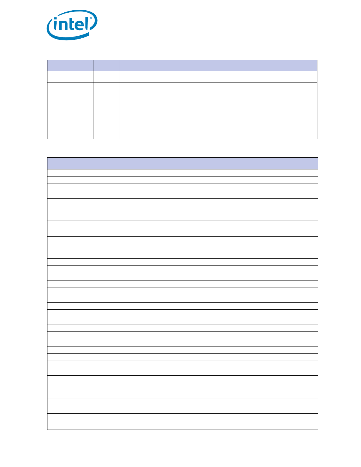
Table 1. User Addressable Secto rs
Unformatted Capacity
(Total User Addressable Sectors in LBA Mode)
80GB
156,301,488
120GB
234,441,648
160GB
312,581,808
240GB
468,862,128
300GB
586,072,368
400GB
781,422,768
480GB
937,703,088
600GB
1,172,123,568
800GB
1,562,824,368
Table 2.
Random Read/W rite Input/Output Opera t ions Per Second (IOPS)
Intel SSD DC S3500 Series
80GB
1.8”)
240GB
1.8”)
800GB
1.8”)
Random 4KB Read (up to)2
IOPS
70,000
75,000
75,000
75,000
75,000
75,000
75,000
75,000
Random 4KB Write (up to)
IOPS
7,000
4,600
7,500
7,500
9,000
11,000
11,000
11,500
Random 8KB Read (up to)3
IOPS
39,000
47,000
47,500
47,500
47,500
47,500
47,500
47,500
Random 8KB Write (up to)
IOPS
3,700
2,300
3,800
3,800
4,400
5,500
5,500
5,500
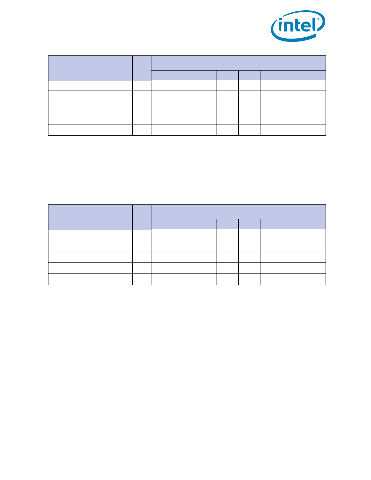
2.0 Product Specifications
2.1 Capacity
Intel® SSD DC S3500 Series
Notes: 1GB = 1,000,000,000 bytes; 1 sector = 512 bytes.
LBA count shown represents total user storage capacity and will remain the same throughout the life of the drive.
The total usable capacity of the SSD may be less than the total physical capacity because a small portion of the capacity is
used for NAND flash management and maintenance purposes.
2.2 Performance
Specification1 Unit
Notes: 1. Performance measured using Iomet er* wi t h Queue Dep t h 3 2 . Mea s u rements are performed on a full Logical Block
Address (LBA) span of the drive.
2. 4KB = 4,096 bytes
3. 8KB = 8,192 bytes
4. Performance consist en cy measured using Iometer* based on Random 4KB QD=32 workload, measured as the (IOPS in
the 99.9th percentile slowest 1-second interval)/(avera g e IOP S d uring t h e test). Measurements are performed on a full
Logical Block Address (LBA) span of the drive once the workload has reached steady state but including all background
activities required for normal operation and data reliability
(2.5/
120GB 160GB
(2.5”/
300GB
400GB
(1.8”)
480
/600GB
(2.5”/
Product Specification March 2014
6 328860-004
Page 7
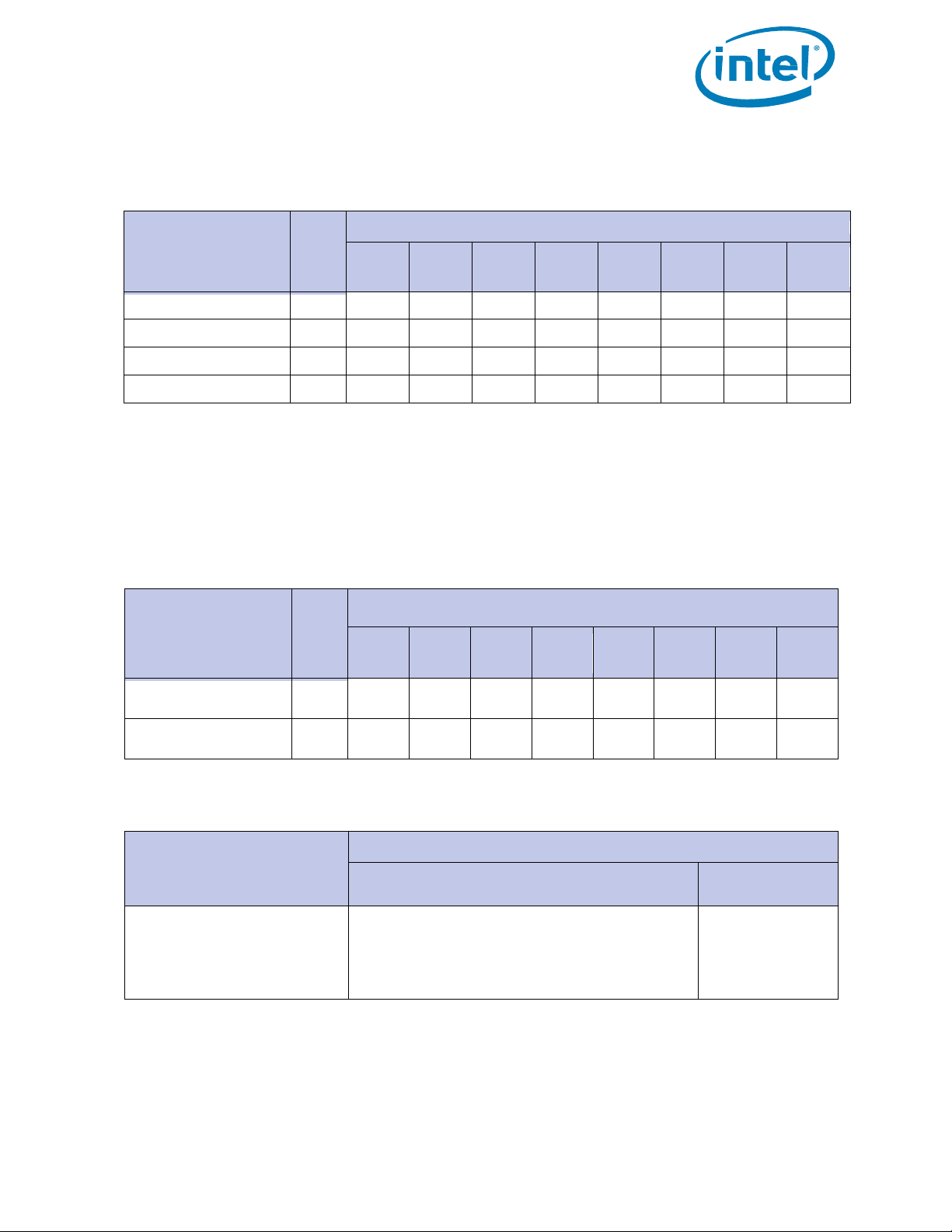
Table 3. Random Read/W rite IOPS Consistency
Intel® SSD DC S3500 Series
80GB
1.8”)
240GB
1.8”)
800GB
1.8”)
Random 4 KB Read (up to)2
%
90
90
90
90
90
90
90
90
Random 4 KB Write (up to)
%
80
80
80
80
80
80
80
80
Random 8 KB Read (up to)3
%
90
90
90
90
90
90
90
90
Random 8 KB W rite (up to)
%
80
80
80
80
80
80
80
80
Notes: 1. Performance measured using Iomet er* wi t h Queue Dep t h 3 2 . Mea s u rements are performed on a full Logical Block
second interval)/( average IOPS d uring the tes t). Meas urements are perf orm ed on a
Table 4. Sequential Rea d a nd Write Bandwidth
Intel SSD DC S3500 Series
80GB
1.8”)
240GB
1.8”)
480
GB
800GB
1.8”)
6Gb/s)1
6Gb/s)1
Table 5. Latency
Intel SSD DC S3500 Series
80GB (2.5/1.8”), 120GB, 160GB, 240GB (2.5”/1.8”),
300GB, 400GB (1.8”), 480GB, 600GB
Intel® Solid-State Drive DC S3500 Series
Specification4 Unit
Address (LBA) span of the drive.
2. 4 KB = 4,096 bytes
3. 8 KB = 8,192 bytes
4. Performance consistency measured using Iometer* based on Random 4KB QD=32 workload, measured as the (IOPS
in the 99.9th p ercen til e sl owes t 1full Logical Block Address (LBA) span of the drive once the workload has reached steady state, including all background
activities required for normal operation and data reliability
Specification Unit
Sequential Read (SATA
(2.5/
(2.5/
MB/s 340 445 475 500 500 500 500 500
120GB 160GB
120GB 160GB
(2.5”/
(2.5”/
300GB
300GB
400GB
(1.8”)
400GB
(1.8”)
480 /
600 GB
/600
(2.5”/
(2.5”/
Seque ntial Wr i t e (SATA
Notes: 1. Performance measured using Iometer* with 128 KB (131,072 bytes) of transfer size with Queue Depth 32.
Specification
Latency1 (TYP)
Read
Write
Power On to Ready
MB/s 100 135 175 260 315 380 410 450
800GB (2.5”/1.8”)
50 µs
65 µs
2
2.0 s
March 2014 Product Specification
328860-004 7
50 µs
65 µs
3.0 s
Page 8
Intel® Solid-State Drive DC S3500 Series
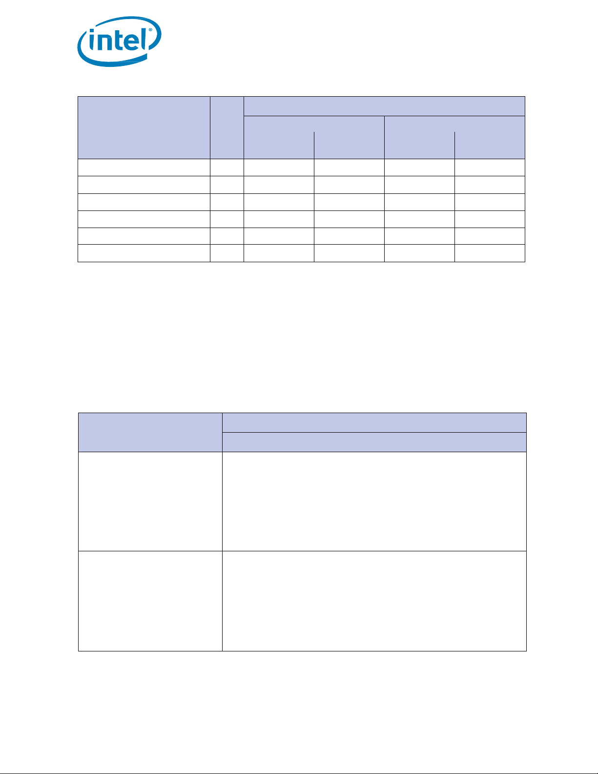
Table 6. Quality of Service
Intel® SSD DC S3500 Series
Queue Depth=1
Queue Depth=32
80/120/160/
240GB
300/400/480/
600/800GB
80/120/160/
240GB
300/400/480/
600/800GB
Quality of Service
(99.9%)
Reads
ms
0.5
0.5 2 2
Writes
ms 5 2
20
10
Quality of Service
(99.9999%)
Reads
ms
10 5 10
5
Writes
ms
10
10
30
30
Table 7. Operating Voltage for 2.5-inch Form Fa c tor
Intel SSDDC S3500 Series
80GB, 120GB, 160GB, 240GB, 300GB, 480GB, 60 0G B, 800GB
Inrush Current (Typical Peak) 1
1.0 A, < 1 s
Inrush Current (Typical Peak) 1
1.0 A, < 1 s
Specification Unit
3, 4
3,4
Notes:
1. Device measured using Iometer. Latency measured using 4KB (4,096 bytes) transfer size with Queue Depth equal to 1 on a
sequential workload.
2. Power On To Ready time assumes proper shutdown. Time v aries if shutdow n is not preceded by STANDBY IMMEDI ATE command.
For 95% of the time, the maximum time fo r pow er on t o ready will be less than 10 seconds.
3. Device measured using Iometer. Quality of Service m easured using 4KB (4,096 bytes) transfer size on a random workload on a full
Logical Block Address (LBA) span of the drive once the workload has reached steady state but including all background activities
required for normal operation and data reliability.
4. Based on Random 4KB QD=1, 32 workloads, measured as the time taken for 99.9(or 99.9999) percentile of commands to finish
the round-trip from host to drive and back to host.
2.3 Electrical Characteristics
Electrical Characteristics
5 V Operating Characteristics:
Operating Voltage range
Rise time (Max/Min)
Fall time (Min)
Noise level
Min Off time
2
500 mV pp 10 Hz – 100 KHz
3
50 mV pp 100 KHz – 20 MHz
12 V Operating Characteristics:
Operating Voltage range
Rise time (Max/Min)
Fall time (Min)
Noise level
Min Off time
Notes:
2
1000 mV pp 10 Hz – 100 KHz
3
100 mV pp 100 KHz – 20 MHz
500 ms
1. Measured from initial device power supply application.
2 Fall time needs to be equal or better than minimum in order to guarantee full functionali ty of enhanced power loss management.
3 The drive needs to be powered off for at least 500msec before powering on.
5 V (±5%)
1 s / 1 ms
1 ms
500 ms
12 V (±10%)
1 s / 1 ms
1 ms
Product Specification March 2014
8 328860-004
Page 9
Intel® SSD DC S3500 Series
80GB
120GB
160GB
240GB
300GB
480GB
600GB
800GB
Active Write - RMS Average 1
W
1.8
2.0
2.3
2.9
3.5
4.3
4.5
5.0
Active Write - RMS Burst 2
W
2.0
2.4
2.7
3.2
3.9
5.2
5.5
7.3
Active Read - RMS Average 3
W
1.5
1.5
1.6
1.6
1.6
1.6
1.6
1.6
Active Read - RMS Burst 4
W
1.8
2.2
2.5
2.8
3.0
3.3
3.4
3.5
Idle
W
Intel SSD DC S3500 Series
80GB
120GB
160GB
240GB
300GB
480GB
600GB
800GB
Active Write - RMS Average1
W
Active Write - RMS Burst2
W
2.2
2.5
2.8
3.4
4.2
5.5
6.8
7.8
Active Read - RMS Average3
W
1.6
1.6
1.7
1.7
1.7
1.7
1.7
1.8
Active Read - RMS Burst4
W
2.1
2.3
2.6
3.2
3.6
3.6
3.6
6.4
Idle
W
0.8
0.8
0.9
0.9
0.9
0.9
0.9
0.9
Intel® Solid-State Drive DC S3500 Series
Table 8. Power Consumption for 2.5-inch Form Factor (5V Suppl y )
Specification Unit
0.6 0.6 0.6 0.6 0.6 0.6 0.6 0.6
Notes:
1. The workload equates 128KB (131,072 bytes) Queue Depth equal to 32 sequential writes. Root Mean Squared (RMS) average
power is measured using scope trig g er ov er a 100 ms sam ple period.
2. The workload equates 128KB (131,072 bytes) Queue Depth equal to 32 sequential writes. Root Mean Squared (RMS) burst power
is measured using scope tri gger ov er a 5 0 0 us sample period.
3. The workload equates 128KB (131,072 bytes) Queue Depth equal to 32 sequential reads. Root Mean Squared (RMS) average
power is measured using scope trigger over a 100 ms sample period.
4. The workload equates 128KB (131,072 bytes) Queue Depth equal to 32 sequential reads. Root Mean Squared (RMS) burst power
is measured using scope tri gger ov er a 5 0 0 us sample period.
Table 9. Power Consumption f or 2.5-inch Form Factor (12V Supply)
Specification1 Unit
2.0 2.3 2.5 3.1 3.5 4.3 4.5 5.0
Notes:
1. The workload equates 128 KB (131,072 bytes) Queue Depth equal to 32 sequential writes. Root Mean Squared (RMS) average
power is measured using scope trig g er ov er a 100 ms sam ple period.
2. The workload equates 128 KB (131,072 bytes) Queue Depth equal to 32 sequential writes. Root Mean Squared (RMS) burst power
is measured using scope trigger over a 500 us sample period.
3. The workload equates 128 KB (131,072 bytes) Queue Depth equal to 32 sequential reads. Root Mean Squared (RMS) average
power is measured using scope trig g er ov er a 100 ms sam ple period.
4. The workload equates 128 KB (131,072 bytes) Queue Depth equal to 32 sequential reads. Root Mean Squared (RMS) burst power
is measured using scope tri gger ov er a 5 0 0 us sample period.
March 2014 Product Specification
328860-004 9
Page 10
Table 10. Operating Vol tage and Power Cons umption for 1.8-inch Form Facto r
Electrical Characteristics
Intel® SSD DC S3500 Series
80GB
240GB
400GB
800GB
500 ms
Inrush Current (Typical Peak) 1
1.2 A, < 1 s
Intel SSD DC S3500 Series
80GB
240GB
400GB
800GB
Active Write - RMS Average @ 3.3V
W
2.0
3.5
4.5
5.2
Active Write - RMS Burst @ 3.3V
W
2.2
3.8
5.0
7.5
Active Read - RMS Average @ 3.3V
W
1.3
1.4
1.4
1.4
Active Read - RMS Burst @ 3.3V
W
1.8
2.6
3.0
3.0
Idle @ 3.3V
W
0.6
0.6
0.6
0.6
Intel® Solid-State Drive DC S3500 Series
Operating Voltage for 3.3 V (±5%)
Min
Max
Rise time (Max/Min)
Fall time (Min)
Noise level
Min Off time
Notes:
1. Measured from initial device power supply application.
2. F all time n eeds to be equal or better than mi nimum in order to guarantee full functionalit y of enhanced power loss management.
3. The drive needs to be powered off fo r at least 5 0 0msec before powering on.
2
300 mV pp 10 Hz – 100 KHz
3
500 mV pp 100 KHz – 20 MHz
3.13 V
3.47 V
1 s / 1 ms
1 ms
Table 11. Power Consumption for 1.8-inch Form Factor
Specification1 Unit
Notes:
1. The workload equates 128 KB (131,072 bytes) Queue Dep th equ al to 32 sequenti al writes . Root Mean Squared (RMS) power
is measured using scope tri gger ov er a 1 0 0 ms sample period.
Product Specification March 2014
10 328860-004
Page 11

Table 12. Temperature, Shock, Vibration
Temperature
Range
Non-operating1
-55 – 95 oC
Non-operating
30 oC/hr (Typical)
Non-operating
5 – 95 %
Shock and Vibration
Range
Non-operating
1,000 G (Max) at 0.5 msec
Non-operating
3.13 G
RMS
(5-800 Hz) Max
Table 13. Product Regulatory Complianc e Specifications
Region For Which
Conformity Declared
Standard Digital Apparatus
measurement CISPR24:2010
measurement CISPR24:2008 (Modified)
— Part 1: General Requirements
Intel® Solid-State Drive DC S3500 Series
2.4 Environme nt al Conditi ons
Case Temperature
Operating
Temperature Gradient
Operating
Humidity
Operating
3
Shock
Operating
Vibration
Operating
Notes:
1. Please contact your Intel representative for details on the non-operating temperature range.
2. Temperature gradient measured without condensation.
3. Shock specifications assume the SSD is mounted securely with the input vibration applied to the drive-mounting screws. Stimulus
4. Vibration specifications assume the SSD is mounted securely with the input vibration applied to the drive-mounting screws.
4
may be applied in the X, Y or Z axis. Shock specification is measured using Root Mean Squared (RMS) value.
Stimulus may be applied in the X, Y or Z axis. Vibration specificatio n is meas ured us ing RMS value.
2
30 oC/hr (Typical)
1,000 G (Max) at 0.5 msec
2.17 G
0 – 70 oC
5 – 95 %
(5-700 Hz) Max
RMS
2.5 Product Regulatory Compliance
Intel® SSD DC S3500 Series meets or exceeds the regulatory or certific ation
requirements in Table 13.
Title Description
TITLE 47-Telecommunications CHAPTER 1— FEDERAL
COMMUNMICATIONS COMMISSION PART 15 — RADIO
FREQUENCY DEVICES
ICES-003, Issue 4 Interference-Causing Equipment
IEC 55024 Information Technology Equipment —
Immunity characteristics— L imits an d m ethods o f
IEC 55022 Information Technology Equipment — Radio
disturbance Characteristics— Limits and methods of
EN-60950-1 2nd Edition
UL/CSA EN-60950-1 2nd Edition
March 2014 Product Specification
328860-004 11
FCC Part 15B Class B
CA/CSA-CEI/IEC CISPR 22:02. This is CISPR
22:1997 with Canadian Modifications
EN-55024: 1998 and its amendments European Union
EN-55022: 2006 and its amendments European Union
Information Technology Equipment — Safety
Information Technology Equipment — Safety
— Part 1: General Requirements
USA
Canada
USA/Canada
USA/Canada
Page 12

Table 14. Reliability Specifications
to the host.
Test (RDT).
Power On/Off Cycles is defined as power being removed from the
SSD, and then restored . Most host sy stems rem ove p ower from the
shutdown.
endurance.
while running JESD218 standard1
2.6 Reliability
Intel® SSD DC S3500 Series meets or exceeds SS D endurance and data retent ion
requirements as specified in the JESD218 standard. Reliability specifications a r e
Uncorrectable Bit Error Rate (UBER)
listed in the table b e low:
Parameter Value
Intel® Solid-State Drive DC S3500 Series
Uncorrectable bit error rate will not exceed one secto r i n the
specified number of bits read. In the unlikely event of a
non-recoverable read error, the SSD will report it as a read failure to
the host; the sector in error is considered corrupt and is not returned
Mean Time Between Failures ( M T BF)
Mea n T i me Between Failures is estimated based o n Telc ordia*
methodology and demonstrated through Reliability Demonstration
Power On/Off Cycles
SSD when entering suspend and hibernate as well as on a system
Insertion Cycles
SATA /power cable insertion/rem oval cycles.
Data Retention
The time period for retaining data in the NAND at maximum rated
17
< 1 sector per 10
2,000,000 hours
24 per day
50 on SATA cable
500 on backplane
3 months power-off retention once SSD
reaches rated write endurance at 40 °C
bits read
Endurance Rating
Based on JESD219 workload.
1. Refer to JESD218 standard table 1 for UBER, FFR and other Enterprise SSD requirements
Product Specification March 2014
12 328860-004
80 GB: 45 TBW
120 GB:70 TBW
160 GB: 100 TBW
240 GB: 140 TBW
300 GB: 170 TBW
400 GB: 225 TBW
480 GB: 275 TBW
600 GB: 330 TBW
800 GB: 450 TBW
Page 13

Intel® Solid-State Drive DC S3500 Series
2.7 Temperature Sensor
The Intel® SSD DC S3500 Series has an internal temperature sensor with an accuracy of
+/-2C over a range of -20C to +80C which can be monitored u sing two SMART a ttributes:
Airflow Temperature (BEh) and Device Internal Temperatur e ( C2h).
For more information on supported SMART attr ib utes, see “SMART Attributes” on
page 20.
2.8 Power Loss Capacitor Test
The Intel SSD DC S3500 Series s upports testing of the power loss capacitor, w hich can be
monitored using the following SMA R T a ttr ibute: (175, AFh).
2.9 Hot Plug Support
Hot Plug insertion and removal is suppor ted in the presence of a p r op er connector and
appropriate operating system (OS), as described in the SATA 3.0 specification.
This product supports asynchronous signal recovery and issues an unsolicited COMINIT
when first mated with a powered connector to guarantee reliable det ec tion by a host
system without hardware device detection.
March 2014 Product Specification
328860-004 13
Page 14

Intel® Solid-State Drive DC S3500 Series
3.0 Mechanical Information
Figures 1 and 2 show the physical package information for the Intel® SSD DC S3500
Series in the 2.5-inch and 1.8-inch form factor s . All dimensions are in m illimeters.
Figure 1: Intel SSD DC S3500 Series 2.5-inch Dimensions
X – Length -- * Y - Width Z - Height
100.45 Max 69.85 +/- 0.25 7.0 +0/-0.5
* - does not include 0.3 connector protrusion
Product Specification March 2014
14 328860-004
Page 15

Intel® Solid-State Drive DC S3500 Series
Figure 2: Intel® SSD DC S3500 Series 1.8 inch Dimensions
X - Length Y - Width Z - Height
78.50 +/- 0.60 54.0 +/- 0.25 5.0 +/- 0.35
March 2014 Product Specification
328860-004 15
Page 16

Intel® Solid-State Drive DC S3500 Series
4.0 Pin and Signal Descriptions
4.1 2.5-inch Form Factor Pin Locations
Figure 3: Layout of 2 . 5-inch Form Factor Signal and Power Segment Pins
Note: 2.5-inch connector supports built in latching capability.
4.2 1.8-inch Form Factor Pin Locations
Figure 4: La yout of 1.8-inch Form Factor Signal and Power Segment Pins
Product Specification March 2014
16 328860-004
Page 17

Factors
S1
Ground
1st mate
S2
A+
S3
A-
S4
Ground
1st mate
S5
B-
S6
B+
S7
Ground
1st mate
Table 16. Serial ATA Power Pin Definitions—2.5-inc h Form Factors
P12
Not connected
(3.3 V Power)
--
P22
Not connected
(3.3 V Power)
--
P32
Not connected
(3.3 V Power; pre-charge)
2nd Mate
P4
Ground
Ground
1st Mate
P53
Ground
Ground
1st Mate
P63
Ground
Ground
1st Mate
P7
V5
5 V Power
1st Mate
P8
V5
5 V Power
2nd Mate
P9
V5
5 V Power
2nd Mate
P103
Ground
Ground
1st Mate
P116
DAS/DSS
Device Activity Signal/Disable Staggered Spin-up
2nd Mate
P12
Ground
Ground
1st Mate
P137
V12
12 V Power
1st Mate
P147
V12
12 V Power
2nd Mate
P157
V12
12 V Power
2nd Mate
Intel® Solid-State Drive DC S3500 Series
4.3 Connector Pin Signal Definitions
Table 15. Serial ATA Connector P in Signal Definit ions—2.5-inch and 1.8-inch Form
Pin Function Definition
Differential signal pair A
Differential signal pair B
Note: Key and spacing separate signal and power segments.
4.4 Power Pin Signal Definitions
Pin1 Function Definition Mating Order
3,4
3,5
3,5
3,5
3,4
Notes:
1. All pins are in a single row, with a 1.27 mm (0.050-inch) pitch.
2. Pins P1, P2 and P3 are connected together, although they are not connected internally to the device. The host may put 3.3 V on
these pins.
3. The mating sequence is:
• ground pins P4-P6, P10, P12 and the 5V power pin P7
• signal pins and the rest of the 5V power pins P8-P9
4. Ground connectors P4 and P12 may contact before the other 1st mate pins in both the power and signal connectors to
discharge ESD in a suitably configured backplane connector.
5. Power pins P7, P8, and P9 are internally connected to one another within the device.
6. The host may ground P11 if it is not used for Device Activity Signal (DAS).
7. Pins P13, P14 and P15 are internally connected to one another within the device. The host may put 12 V on these pins.
March 2014 Product Specification
328860-004 17
Page 18

Intel® Solid-State Drive DC S3500 Series
Table 17. Serial ATA Power Pin Definitions—1.8-inc h Form Factors
P12
V33
3.3 V Power
2nd Mate
P22
V33
3.3 V Power, per-charge
2nd Mate
P33
Ground
--
1st Mate
P43
Ground
--
1st Mate
P54
V5
5 V Power; not connected.
1st Mate
P64
V5
5 V Power; not connected.
2nd Mate
P75
DAS/DSS
Device Activity Signal/Disable Staggered Spin-up
2nd Mate
Key
Key
NC
NC
P86
Optional
Manufacturing Test Pin
2nd Mate
P96
Optional
Manufacturing Test Pin
2nd Mate
Pin Function Definition Mating Order1
Notes:
1. All mate sequences assume zero angular offset between connectors.
2. P1 and P2 are internally connected to one another within the device.
3. Ground connectors P3 and P4 may contact before the other 1st mate pins in both the power and signal connectors to dis-
charge ESD in a suitably configure backplane connector.
4. Pins P5 and P6 are not connected internally to the device but there is an option to connect through a zero ohm stuffing
resistor. The host may put 5V on these pins.
5. The host may ground P7 if it is not used for Device Activity Signal (DAS).
6. P8 and P9 should not be connected by the host.
Product Specification March 2014
18 328860-004
Page 19

Intel® Solid-State Drive DC S3500 Series
5.0 Supported Command Sets
Intel® SSD DC S3500 Series supports all mandatory ATA (Advanced Technology
Attachment) commands def ined in the A TA8-ACS specificati on desc ribed in th is s ecti on .
5.1 ATA General Feature Command Set
The Intel SSD DC S3500 Series supports the ATA General Feature command set (nonPACKET), which consists of:
− EXECUTE DEVICE DIAGNOSTIC
− SE T FEATU RES
− IDENTIFY DEVICE
Note: See Appendix A, “IDENTIFY DEVICE Command Data” on page 29 for details on
the sector data returned after issuing an IDENTIFY DEVICE command.
Intel SSD DC S3500 Series also supports the following optiona l commands:
− READ DMA
− WRITE DMA
− READ SECTOR(S)
− READ VERIFY SECTOR(S)
− READ MULTIPLE
− SEEK
− SE T FEATU RES
− WRITE SECTOR(S)
− SET MULTIPLE MODE
− WRITE MULTIPLE
− FLUSH CACHE
− READ BUFFF E R
− WRITE BUFFER
− NOP
− DOWNLOAD MICROCODE
− WRITE UNCORRECTABLE EXT
1. The only multiple supported will be multiple 1
1
5.2 Power Management Command Set
Intel SSD DC S3500 Series supports the Power Management command s et, w hich
consists of:
− CHECK POWER MODE
− IDLE
− IDLE IMMEDIATE
− SLEEP
− STANDBY
− STANDBY IMMEDIATE
5.3 Security Mode Feature Set
Intel SSD DC S3500 Series supports the Sec urity Mod e comman d set, wh ich consists of:
− SECURITY SET PASSWORD
− SECURITY UNLOCK
− SECURITY ERASE PREPARE
− SECURITY ERASE UNIT
− SECURITY FREEZE LOCK
− SECURITY DISABLE PASSWORD
March 2014 Product Specification
328860-004 19
Page 20

5.4 SMART Command Set
Table 18. SMART Attributes
SP
EC
ER
PE
OC
PW
remaining of allowable grown defect count.
Normalized value: always 100.
Normalized value: always 100.
AAh
Available Reserved Space (See Attribute E8)
1 1 0 0 1 1 10
Program Fail Count
remaining of allowable program fails.
Erase Fail Count
remaining of allowable erase fails.
Unexpect ed P ower Loss
Normalized value: always 100.
Power Loss Protection Failure
s
1: Last test result as microseconds to discharge
25 <= result <= 5000000, lower indicates specific error
Intel® SSD DC S3500 Series supports the SMA RT command set, which consists of:
− SMART READ DATA
− SMART READ ATTRIBUTE THRESHOLDS
− SMART ENABLE/DISABLE ATTRIBUTE AUTOSAVE
− SMART SAVE ATTRIBUTE VALUES
− SMART EXECUTE OFF-LINE IMMEDIATE
− SMART READ LOG SECTOR
− SMART WRITE LOG SECTOR
− SMART ENABLE OPERATIONS
− SMART DISABLE OPERATIONS
− SMART RETURN STATUS
− SMART ENABLE/DISABLE AUTOMATIC OFFLINE
5.4.1 SMART Attributes
Table 18 lists the SMART attributes supported by the Intel SSD DC S3500 Series and the
corresponding status flags and th reshold settings.
Intel® Solid-State Drive DC S3500 Series
ID Attribute
Re-allocated Sector Count
05h
09h
0Ch
ABh
ACh
AEh
Raw value: shows the number of retired blocks since
leaving the factory (grown defect count).
Normalized value: b eginni ng at 10 0, show s th e perc ent
Power-On Hours Count
Raw value: reports power-on time, cumulative over the life
of the SSD, integer number in hour time units.
Power Cycle Count
Raw value: reports the cumulative number of power cycle
events over the life of the devi ce.
Raw value: shows total count of program fails.
Normalized value: beginning at 100, shows the percent
Raw value: shows total count of erase fails.
Normalized value: beginning at 100, shows the percent
Also known as “Power-off Retract Count” per magnetic-drive terminology.
Raw value: reports number of unclean shutdowns, cumulative ov er the life o f the SSD.
An “unclean shutdown” is the removal of power without
STANDBY IMMEDIATE as the last command (regardless of
PLI activity using capacitor power).
Status Flag s
Threshold
1 1 0 0 1 0 0 (none)
1 1 0 0 1 0 0 (none)
1 1 0 0 1 0 0 (none)
1 1 0 0 1 0 0 (none)
1 1 0 0 1 0 0 (none)
1 1 0 0 1 0 0 (none)
Last test result as microsecond s to discharg e cap, satura te
at max value. Also logs minutes since last test and lifetime
AFh
number of tests.
Raw value:
Bytes 0-
cap, saturates at max value. Test result expected in range
Product Specification March 2014
20 328860-004
1 1 0 0 1 1 10
Page 21

Table 18. SMART Attributes
SP
EC
ER
PE
OC
PW
code.
SATA Downshift Count
Normalized value: alw ays 100.
Normalized value: alw ays 100.
Uncorrectable Error Count
Normalized value: alw ays 100.
Temperature - Airflow Temperature (Case)
Normalized value: 100 – case temperature in C degrees.
Normalized value: always 100.
device temperature in C deg rees,
100 if device temperature less than 50.
Normalized value: always 100.
Normalized value: always 100.
Normalized value: always 100.
Intel® Solid-State Drive DC S3500 Series
ID Attribute
Bytes 2-3: Minutes since last test, saturates at max
value.
Bytes 4-5: Lifetime number of tests, no t inc r emented on
power cycle, saturates at max value.
Normalized value: set to 1 on test failure or 11 if the
capacitor has been tested in an excessive temperature
condition, ot herwise 100.
B7h
B8h
BBh
BEh
Raw value: reports number of times SATA interface
selected lower signaling rate due to error.
End-to-End Error Detection Count
Raw value: reports number of End-to-End detected and
corrected errors by hardware.
Raw value: shows the number of errors that could not
be recovered using Error
Correction Code (ECC).
Raw value: reports SSD case temp erature statisti c s.
Bytes 0-1: Current case temperature, Celsius
Byte 2: Recent min case temperature, Celsius
Byte 3: Recent max case temperature, Celsius
Bytes 4-5: Over temperature counter. Number of times
sampled temperature exceeds drive max operating tem-
perature specification.
Status Flag s
Threshold
1 1 0 0 1 0 0 (none)
1 1 0 0 1 0 0 (none)
1 1 0 0 1 0 0 (none)
1 0 0 0 1 0 0 (none)
Power-Off Retract Count (Unsafe Shutdown Count)
Raw value: reports the cumulative number of unsafe
C0h
C2h
C5h
C7h
E1h
(unclean) shutdown events over the life of the device. An
unsafe shutdown occurs whenever the device is powered
off without STANDBYIMMEDIATE being the last command.
Temperature - Device Internal Temperature
Raw value: Reports internal temperature of the SSD in
degrees Celsius. Temp er at u re r eading is the value direct
from the printed circuit board (PCB) sensor without offset.
Normalized value: 150 –
Pending Sector Count
Raw value: number of current unrecoverable read errors
that will be re-allocated on next write.
CRC Error Count
Raw value: shows total number of encountered SATA
interface cyclic redundancy check (CRC) errors.
Host Writes
Raw value: reports total number of sectors written by the
host system. The raw value is inc rease d by 1 for every
65,536 sectors (32MB) written by the host.
March 2014 Product Specification
328860-004 21
1 1 0 0 1 0 0 (none)
1 0 0 0 1 0 0 (none)
0 1 0 0 1 0 0 (none)
1 1 0 0 1 0 0 (none)
1 1 0 0 1 0 0 (none)
Page 22

Intel® Solid-State Drive DC S3500 Series
Table 18. SMART Attributes
SP
EC
ER
PE
OC
PW
Normalized value: always 100.
Normalized value: always 100.
Normalized value: always 100.
threshold value for this attribute is 10 percent availability.
wear can be put on the device.
Normalized value: always 100.
reports the total number of sectors written by
the host system. The raw value is increased by 1 for every
Normalized value: always 100.
Normalized value: always 100.
ID Attribute
Timed Workload Media Wear
Raw value: measures the wear seen by the SSD (since
reset of the workload timer, attribute E4h), as a
E2h
E3h
E4h
E8h
E9h
percentage of the maximum rated c ycles. Divide the raw
value by 1024 to derive the perc entag e with 3 decimal
points.
Timed Workloa d Host Read/Write Ra tio
Raw value: shows the percentage of I/O operations that
are read operations (si nce reset of the workload timer,
attribute E4h). Reported as integer percentage from 0 to
100.
Timed Workload Timer
Raw value: measures the elapsed time (number of
minutes since starting this workload timer).
Available Reserved Space
Raw value: reports number of reserve blocks remaini ng.
Normalized value: begins at 100 , which corresponds to
100 percent availability of the reserved space. The
Media Wearout Indicator
Raw value: always 0.
Normalized value: reports the number of cycles the NAND
media ha s under gone. Declines linearly from 100 to 1 as the
average erase cycle count i ncreases from 0 to the
maximum rated cycles.
Once the nor malized value reaches 1, the number will not
decrease, although it is likely that sig nificant additiona l
Status Flag s
Threshold
1 1 0 0 1 0 0 (none)
1 1 0 0 1 0 0 (none)
1 1 0 0 1 0 0 (none)
1 1 0 0 1 1 10
1 1 0 0 1 1 1
Thermal Throttle Status
Raw value: reports Percent Throttle Status and Count of
events
EAh
F1h
F2h
Byte 0: Throttle status reported as integer percentage.
Bytes 1-4: Throttling event count. Number of times
thermal throttle has acti vated. Preserved over power cycles.
Byte 5: Reserved.
Total LBAs Written
Raw value:
65,536 sectors (32MB) written by the host.
Total LBAs Read
Raw value: reports the total number of sectors read by the
host system. The raw value is inc rease d by 1 for every
65,536 sectors (32MB) read by the host.
Product Specification March 2014
22 328860-004
1 1 0 0 1 0 0 (none)
1 1 0 0 1 0 0 (none)
1 1 0 0 1 0 0 (none)
Page 23

Table 19. SMART Attribute Status Flags
SP
Self-preserving attribute
Not a self-preserving attribute
Self-preserving attribute
EC
Event count attribute
Not an event count attribute
Event count attribute
ER
Error rate attribute
Not an error rate attribute
Error rate attribute
PE
Performance attribute
Not a performance attribute
Performance attribute
online activity
PW
Pre-fail warranty attribute
Advisory
Pre-fail
Intel® Solid-State Drive DC S3500 Series
Status Flag Description Value = 0 Value = 1
OC
Online collection attribute Collected only during offline activity
5.4.2 Timed Workload Endurance Indicators
Timed Workload Medi a Wear Indicator — ID E2h
This attribute tracks the driv e wear seen by the device during the last wear timer loop, as
a percentage of the maximum rated cycles. The raw value tracks the percentage up to 3
decimal points. This va lu e sh ou ld be div ided by 1024 to get the percentage.
For example: if the raw va lue is 4450, the percen tage is 4450/10 24 = 4.345%. The raw
value is held at FFFFh until the wear timer (attribute E4h) reaches 60 (minutes) after a
SMART EXECUTE OFFLINE IMMEDIATE (B0h/D4h) subcommand 40h to the SSD. The
normalized value is alway s s et to 100 and should be ignored.
Timed Workload Ho st Reads Percentage — I D E3h
This attribute sh ows the percenta ge of I/O operation s that are read operat ions during the
last workload timer loop. The raw value tracks this percentage and is held at FFFFh until
the workload timer (attribute E 4h) reaches 60 (minutes). T he normalized valu e is always
set to 100 and should be ignored.
Workload Timer — ID E4h
This attribute is u sed to measure the time elapsed during th e c urrent workload. Th e
attribute is reset when a SMART EXECUTE OFFLINE IMMEDIATE (D4h) subcommand 40h
is issued to the driv e. The raw value tracks the time in minu tes and has a maximum value
of 232 = 4,294,967,296 min utes (8,171 years). The normaliz ed value is always set to
100 and should be ignored.
Collected during both offline and
User Notes
• Sending a SMART EXECUTE OFFLINE IMMEDIATE (B0h/D4h) subcommand 40h to the
SSD resets and s tarts all thr ee attribu tes (Media Wear Indic ator, Attr ibute E2h, Host
Reads Percentage, Attribute E3h, and the Workload timer, Attribute E 4 h) to FFFFh.
• The Attribute raw values are held at FFFFh until the Workload timer (Attribute E4h)
reaches a total of 60 (minutes) of power on time. After 60 minutes, the Timed
Workload data is made available.
• After the Workloa d timer (E4h) reaches 60 (minutes), the T im ed W orkload data is
saved every minute so only 59 seconds of data is lost if power is rem oved without
receiving ATA STANDBY IMMEDIATE. Accumulated data is not reset due to power
loss.
• Upon power up, th e a ttr ibutes hold a snaps hot of their last saved va lues for 59
seconds and live d ata is availabl e after 60 s econds, once the in itial one hou r interval
is completed.
March 2014 Product Specification
328860-004 23
Page 24

Intel® Solid-State Drive DC S3500 Series
Example Use Cases
The Timed Workload Endurance attributes des cribed in this sec tion are intended to be
used to measure the amoun t of media wear that th e drive is subjected t o during a timed
workload.
Ideally, the system that th e dr ive is being used in should be capable of iss uing SMART
commands. Oth erwise, provisions have been provided to a llow the media wear attribu tes
to be persistent so the drive can be moved to a SMART capable system to read out the
drive wear attribute valu es .
Use Case 1 – With a System Capable of SMART Com mands
1. On a SMART capable system, issue the SMART EXECUTE OFF-LINE IMMEDIAT E
(D4h) sub-command 40h to reset the drive wear attributes.
2. Run the wor kload to be evaluated f or at least 60 minutes. Otherwise the drive
wear attributes will not be available.
3. Read out the drive wear attributes with the SMART READ DA TA (D0h) command.
Use Case 2 – With a System Not Capable of SMART Commands
1. On a SMART capable system, issue the SMART EXECUTE OFF-LINE IMMEDIATE
(D4h) sub-command 40h to reset the the drive wear attributes.
2. Move the drive to the system wh er e th e workload will be measured (and not
capable of SMART commands).
3. Run the wor kload to be evaluated f or at least 60 minutes. Otherwise the drive
wear attributes will not be available.
4. Do a clean system power down by issuing the ATA STANDBY IMMEDIATE
command prior to s hutting down the sy stem. This will store all the dr ive wear
SMART attributes to persistent memory within the drive.
5. Move the drive to a SM ART capable system.
6. Read out the driv e wear at tributes wi th the S MART REA D DATA (D0h) command
within 59 seconds a fter power-up.
Example Calculation of Drive Wear
The following is a n example of how th e drive wear attr ibutes can be used to evaluate th e
impact of a given workload. The Host Writes SMART a ttr ibute (E1h) can a lso be used to
calculate the amount of data written by the host during the w or kload by reading this
attribute before and after running the workload. This example as s umes that the steps
shown in “Ex ample Use Cases” on page 18 were f ollowed to obta in the follow ing attribute
values:
• Timed Workload Media Wear (E2h) has a raw va lu e of 16. T herefore, the percentage wear = 16/1024 = 0.016%.
• Timed Workload Host Read/Write Ratio (E3h) h as a normalized value of 80, indicating that 80% of operations w er e r ea ds .
• Workload T imer (E 4h) has a raw va lue of 500. Therefore the w orkload ran for 500
minutes.
• Host Writes Count ( E1h) had a raw va lue of 100,000 prior to ru nning the workloa d
and a value of 130,000 at the end of the workload. Therefore, the nu m ber of
sectors written b y the host during the workload was 30,000 * 65,535 =
1,966,050,000 sectors or 1,966,050,000 * 512/1,000, 000, 000 = 1,007 GB.
The following con clusions can be mad e for this example case:
The workload took 5 00 minutes to compl e te with 80% reads and 20% writes. A total of
1,007 GB of data was written to the device, wh ich increased the media wea r in the drive
Product Specification March 2014
24 328860-004
Page 25

Table 20. Device Statistics Log
Equivalent SMART
applicable)
0x00
--
List of Supported Pages
--
0x08
Power Cycle Count
0Ch
0x10
Power-On Hours
09h
0x18
Logical Sectors Written
E1h
for every host write
0x28
Logical Sectors Read
F2h
for every host read
and Completion
Intel® Solid-State Drive DC S3500 Series
by 0.016%. At this point in time, this workload is causing a wear rate of 0. 016% for every
500 minutes, or 0.00192%/ hour.
5.4.3 SMART Logs
Intel SSD DC S3500 Series implements the following L og Addresses: 00h, 02h, 03h , 06h,
and 07h.
DC S3500 Series imple ments host v endor specific logs (a ddresses 80h-9Fh) as read and
write scratchpads, where the default value is zero (0). Intel SSD DC S3500 does not write
any specific values to these logs u nless directed by the host through the appropriate
commands.
DC S3500 Series also implements a device vendor specific log at address A9h as a
read-only log area with a default value of zer o ( 0 ) .
5.5 Device Statistics
In addition to the SMART attribute structure, statistics pertaining to the ope r ation and
health of the Intel SSD DC S3500 Series can be repor ted to the host on reques t throu gh
the Device Statis tics log as defined in the ATA specification.
The Device Statistic s log is a read-only GPL/SMA RT log located at read log address 0x04
and is accessible using READ LOG EXT, READ LOG DMA EXT or SMART READ LOG
commands.
Table 20 lists the Dev ic e Statistics supported by the Intel SSD DC S3500 Series.
Page Offset Description
0x01 – General Statistics
0x04 – General Error Statistics
0x05 – Temperature Statistics
0x20
0x30
0x08 Num Reported Uncorrectable Errors BBh
0x10
0x00 Device Statistics Information Header -0x08 Current Temperature -0x10 Average Short Term Temperature -0x18 Average Long Term Temperature -0x20 Highest Temperature -0x28 Lowest Temperature -0x30 Highest Average Short Term Temperature -0x38 Lowest Average Short Term Temperature -0x40 Highest Average Long Ter m Temperat ur e -0x48 Lowest Average Long Term Temperature --
Num Write Commands – incremented by one
Num Read Commands – incremented by one
Num Resets Between Command Accep t a nce
March 2014 Product Specification
328860-004 25
attribute (if
--
--
--
Page 26

Intel® Solid-State Drive DC S3500 Series
Table 20. Device Statistics Log
Equivalent SMART
applicable)
counts from 1 to 150
Page Offset Description
0x50 Time in Over-Temperature -0x58 Specified Maximum Operating Temperature -0x60 Time in Under-Temperature -0x68 Specified Minimum Operating Temperature -0x08 Number of Hardware Resets --
0x06 – Transport Statistics
0x07 – Solid State Device Statistics 0x08 Percentage Used Endurance Indicato r
0x10 Number of ASR Events -0x18 Number of Interface CRC Errors --
5.6 SMART Command Transport (SCT)
With SMART Command Transport (SCT), a host can send commands and data to an SSD
and receive status and data from an SSD using standard write/read commands to
manipulate two SM ART Logs:
− Log Address E0h ("SCT Co mmand/Status") — used to send commands and retrieve status
− Log Address E1h ("SCT Data Transfer") — used to transport data
Intel® SSD DC S3500 Series supports the f ollowing standard SCT actions:
− Write Same — DC S3500 Series implements this action code as described in the ATA
specification
− Error Recovery Control — DC S3500 Series accepts this actio n code, and will store and return
error-recovery time limit values
− Feature Contr ol - DC S3500 Series supports feature code 0001h (write cache) feature code
0002h (write cache reordering), and featur e cod e 0003 h (time interv a l fo r tempe rature
logging). It also supports D000h(Power Safe Write Cache capacitor test interval),
(D001h(read/write power governor mode), D002h(read thermal governor mode), D003h(read
power governor bu rs t po we r), D004h(read power governor average power)
− Data table co mmand - DC S3500 Series supports data table command as specified in
ATA8-ACS2. This will read out temperature logging information in table ID 0002h
− Read Status Support - DC S3500 Series supports read status log
attribute (if
E9h
Note: This device statistic
5.7 Data Set Management Command Set
Intel SSD DC S3500 Series supports the Data Set Management command set Trim
attribute, wh ic h consists of:
− DATA SET MANAGEMENT
5.8 Host Protected Area Command Set
Intel SSD DC S3500 Series supports the Host Protected Area comm a nd set, which
consists of:
− READ NATIVE MAX ADDRESS
− SET MAX ADDRESS
− READ NATIVE MAX ADDRESS EXT
− SET MAX ADDRESS EXT
Intel SSD DC S3500 Series also supports th e following optiona l commands:
− SET MAX SET PASSWORD
− SET MAX LOCK
− SET MAX FREEZE LOCK
− SET MAX UNLOCK
Product Specification March 2014
26 328860-004
Page 27

Intel® Solid-State Drive DC S3500 Series
5.9 48-Bit Address Command Set
Intel® SSD DC S3500 Series supports the 48-bit Address command set, which consists
of:
− FLUSH CACHE EXT
− READ DMA EXT
− READ NATIVE MAX ADDRESS EXT
− READ SECTOR(S) EXT
− READ VERIFY SECTOR(S) EXT
− SET MAX ADDRESS EXT
− WRITE DMA EXT
− WRITE MULTIPLE EXT
− WRITE SECTOR(S) EXT
− WRITE MULTIPLE FUA EXT
− WRITE DMA FUA EXT
5.10 General Purpose Log Command Set
Intel SSD DC S3500 Series supports the General Purpose Log command set, which
consists of:
− READ LOG EXT
− WRITE LOG EXT
5.11 Native Comm and Queuing
Intel SSD DC S3500 Series supports the Native Command Queuing (NCQ) command set,
which includes:
− READ FPDMA QUEUED
− WRITE FPDMA QUEUED
Note: With a maximum Queue Depth set to 32.
5.12 Software Settings Preservation
Intel SSD DC S3500 Series supports the SET FEATURES pa rameter to enable/dis able the
preservation of software settings.
March 2014 Product Specification
328860-004 27
Page 28

Intel® Solid-State Drive DC S3500 Series
Table 21. Device Certifications and Declarations
Certification
Description
COUNCIL of 15 December 2004.
1: General Requirements)
computers or facsim ile.
Table 22. Standards References
(JESD218)
nts/docs/jesd218/
Dec 2008
VCCI
http://www.vcci.jp/vcci_e/
http://qdms.intel.com/
for material description datasheet
6.0 Certifications and Declarations
Table 21 descr ibes the Device Certificat ions supported by th e Intel® SSD DC S3500 Series.
CE Compliant
UL Recognized
C-Tick Compliant
BSMI Compliant
KCC
VCCI
RoHS Compliant Restriction of Hazardous Substance Directive
WEEE Directive on Waste Electrical and Electronic Equipment
Low Voltage DIRECTIVE 2006/95/EC OF THE EUROPEAN PARLIAMENT AND OF THE COUNCIL
of 12 December 2006, and EMC Directive 2004/108/EC OF THE EUROPEAN PARLIAMENT AND OF THE
Underwriters Laboratories, Inc. Bi-National Component Recognition; UL 60950-1, 2nd Edition,
2007-03-27 (Informati on Techn o logy Equipment - Safety - Part 1: General Requirements)
CSA C22.2 No. 60950-1-07, 2nd Edition, 2007-03 (Informa tion Tec hnology Equipm ent - Safety - Part
Compliance with the Australia/New Zealand Standard AS/NZS3548 and Electromagnetic
Compatibility (EMC) Framework requirements of the Australian Communication Authority (ACA).
Compliance to the Taiwan EMC standard CNS 13438: Information technology equipment - Radio
disturbance Characteristics - limits and methods of measurement, as amended on June 1, 2006, is
harmonized with CISPR 22: 2005.04.
Compliance with paragraph 1 of Article 11 of the Electromagnetic Compatibility Control Regulation
and meets the Electromagnetic Compatibility (EMC) Framework requirements of the Radio Research
Laboratory (RRL) Ministry of Information and Communication Republic of Korea.
Voluntary Control Council for Interface to cope with disturbance problems caused by personal
7.0 References
Table 22 identifies th e Standards infor m a tion referenced in this document.
Date Title Location
July 2012
Sept 2010
June 2009 RoHS
August 2009 ACS-2-ATA/ATAPI Command Set 2 Specification http://www.t13.org/
June 2009 Serial ATA Revision 3.0 http://www.sata-io.org/
May 2006 SFF-8223, 2.5-inch Drive w/Serial Attachment Connector http://www.sffcommittee.org/
May 2005 SFF-8201, 2.5-inch drive form factor http://www.sffcommittee.org/
Product Specification March 2014
28 328860-004
Solid-State Drive (SSD) Requirements and Endurance Test Method
(JESD219)
Solid-State Drive (SSD) Requirements and Endurance Test Method
http://www.jedec.org/standards-docume
nts/results/jesd219
http://www.jedec.org/standards-docume
Click Search MDDS Database and search
Page 29

Table 22. Standards References
voltage variations immunity tests)
(Radiated electromagnetic field from digital radio telephones)
radimmun.htm/
Word
F = Fixed
X = Both
Default Value
Description
0 X 0040h
General configuration bit-significant information
1 X 3FFFh
Obsolete - Number of logical cylinders (16,383)
2 V C837h
Specific configuration
3 X 0010h
Obsolete - Number of logical heads (16)
4-5 X 0h Retired
6 X 003Fh
Obsolete - Number of logical sectors per logical track (63)
7-8 V 0h Reserved for assignment by the CompactFlash* Association (CFA)
9 X 0h Retired
10-19 F
varies
Serial number (20 ASCII characters)
20-21 X 0h
Retired
22 X 0h Obsolete
23-26 F
varies
Firmware revision (8 ASCII characters)
27-46 F
varies
Model number (Intel® Solid-State Drive)
commands
48 F 4000h
Trusted Computing F eatur e Set
49 F 2F00h
Capabilities
50 F 4000h
Capabilities
51-52 X 0h
Obsolete
53 F 0007h
Words 88 and 70:64 valid
54 X 3FFFh
Obsolete - Number of logical cylinders (16,383)
55 X 0010h
Obsolete - Number of logical heads (16)
56 X 003Fh
Obsolete - Number of logical sectors per logical track (63)
57-58 X
FC1000FBh
Obsolete
59 F BF01 Number of sectors transferred per interrupt on multiple commands
80GB: 0950F8B0h
800GB: 0FFFFFFFh
Intel® Solid-State Drive DC S3500 Series
Date Title Location
International Electrotechnical Commission EN 61000
1995
1996
1995
1995
1997
1994
4-2 (Electrostatic discharge immunity test)
4-3 (Radiated, radio-frequency, electromagnetic field immunity test)
4-4 (Electrical fast transient/burst immunity test)
4-5 (Surge immunity test)
4-6 (Immunity to conducted disturbances, induced by radio-
frequency fields)
4-11 (Voltage Variations, voltage dips, short interruptions and
http://www.iec.ch/
1995 ENV 50204
http://www.dbicorporation.com/
Appendix A: IDENTIFY DEVICE Command Data
Table 23. Returned Sector Data
V = Variable
47
F
8001h
7:0—Maximum number of sectors transferred per interrupt on multiple
120GB: 0DF94BB0h
160GB: 0FFFFFFFh
240GB: 0FFFFFFFh
300GB: 0FFFFFFFh
400GB: 0FFFFFFFh
480GB: 0FFFFFFFh
600GB: 0FFFFFFFh
60-61
V
March 2014 Product Specification
328860-004 29
Total number of user-addressable sector for 28-bit commands
Page 30

Table 23. Returned Sector Data
Word
F = Fixed
X = Both
Default Value
Description
62 X 0h
Obsolete
63 X 0007h
Multi-w or d D MA modes supported/select e d
64 F 0003h
PIO modes supported
65 F 0078h
Minimum multiword DMA transfer cycle time per word
66 F 0078h
Manufacturer’s recommended multiword DMA transfer cycle time
67 F 0078h
Minimum PIO transfer cycle time without flow control
68 F 0078h
Minimum PIO transfer cycle time with IORDY flow control
69 F 4030h
Additional Supported
70 F 0000h
Reserved
71-74 F 0h
Reserved for IDENTIFY PACKET DEVICE command
75 F 001Fh
Queue depth
76 F 850Eh
Serial ATA capabilities
77 F 0006h
Reserved for future Serial ATA definition
78 F 0040h
Serial ATA features supported
79 V 0040h
Serial ATA features enabled
80 F 03FCh
Major version number
81 F 0110h
Minor version number
82 F 746Bh
Command set supported
84 F 6163h
Command set/feature supported extension
85 X 7469h
Command set/feature enabled
86 X B401h
Command set/feature enabled
87 X 6163h
Command set/feature default
88 X 407Fh
Ultra DMA Modes
89 F 0002h
Time required for security erase unit completion
90 F 0002h
Time required for enhanced security erase completion
91 V 0h Current advanced power management value
92 V 0FFFEh
Master Password Revision Code
93
X
0h
94 V 0h Vendor’s recommended and actual acoustic management value
95 F 0h Stream minimum request size
96 V 0h Streaming transfer time - DMA
97 V 0h Streaming access latency - DMA and PIO
98-99 F 0h
Streaming performance granularity
80GB: 0950F8B0h
800GB: 5D26CEB0h
104 V 0h Streaming transfer time - PIO
SET MANAGEMENT command
106 F 6003h
Physical sector size / logical sector size
107 F 0h Inter-seek delay for ISO-7779 acoustic testing in microseconds
108-111
F varies
Unique ID
112-115
F 0h Reserved for world wide name extension to 128 bits
V = Variable
Intel® Solid-State Drive DC S3500 Series
83
100-103
F
V
7501h
Command sets supported
Hardware reset result: the contents of bits (12:0) of this word shall
change only during the execution of a hardware reset
120GB: 0DF94BB0h
160GB: 12A19EB0h
240GB: 1BF244B0h
300GB: 22EEC130h
400GB: 2E9390B0h
480GB: 37E436B0h
600GB: 45DD2FB0h
Maximum user LBA for 48-bit address feature set
105
V
0004h
Maximum number of 512-byte blocks of LBA Range Entries per DATA
Product Specification March 2014
30 328860-004
Page 31

Word
F = Fixed
X = Both
Default Value
Description
116 V 0h Reserved for technical report
117-118
F 0h Words per logical sector
119 F 405Ch
Supported settings
120 X 401Ch
Command set/feature enabled/supported
121-126
F 0h Reserved
127 X 0h Removable Media Status Notification feature set support
128 X 0021h
Security status
129 V
001Ch
Vendor-specific
130-139
X 0h Vendor-specific
140-149
X
0h
Disable Logical Error Field
150-159
X
0h
Vendor-specific
160 X 0h CompactFlash Association (CFA) power mode 1
161-167
X 0h Reserved for assignment by the CFA
168 X
0003h
Reserved for assignment by the CFA
169 X 0001h
Data set management Trim attribute support
170-175
F 0h Reserved for assignment by the CFA
176-205
V Varies
Current media serial number
206 X 003Dh
SCT Command Transport
207-208
F 0000h
Reserved
209 X 4000h
Alignment of logical blocks within a physical block
210-211
V 0000h
Write-Read-Verify Sector Count Mode 3 (DWord)
212-213
214 X 0000h
NV Cache Capabilities
215-216
V 0000h
NV Cache Size in Logical Blocks (DWord)
217 F 0001h
Nominal media rotation rate
218 V 0000h
Reserved
219 F 0000h
NV Cache Options
220 V 0000h
Write-Read-Verify feature set
221 X 0000h
Reserved
222 F 101Fh
Transport major version number
223 F 0000h
Transport minor version number
224-229
F 0000h
Reserved
230-233
X 0000h
Extended Number of User Addressable Sectors (QWord)
234
F 0001h
command for mode 03h
235
F FFFFh
command for mode 03h
236-254
X 0000h
Reserved
255 V Varies
Integrity word
Intel® Solid-State Drive DC S3500 Series
Table 23. Returned Sector Data
V = Variable
Notes: F = Fixed. The content of the word is fixed and does not change. For removable media devices, these values may change
F
when media is removed or changed.
V = Variable. The state of at least one bit in a word is variable and may change depending on the state of the device or the
commands executed by the device.
X = F or V. The content of the word may be fixed or variable.
0000h
Write-Read-Verify Sector Count Mode 2 (DWord)
Minimum number of 512-byte data blocks per DOWNLOAD MICROCODE
Maximum number of 512-byte data blocks per DOWNLOAD MICROCODE
March 2014 Product Specification
328860-004 31
 Loading...