

Page 1

PR440FX
Motherboard
Technical Product Specification
Order Number: 281829-002
November 1996
The PR440FX motherboard may contain design defects or errors known as errata. Characterized errata that
may cause the PR440FX motherboard’s behavior to deviate from published specifications are documented in
the PR440FX Motherboard Specification Update.
Page 2

Revision History
Revision
001
002
Revision History Date
First release of the PR440FX Specification. 08/96
Second release of the PR440FX Specification 11/96
This product specification applies only to standard PR440FX with BIOS identifier 1.00.0x.DI0.
Changes to this specification will be published in the PR440FX Motherboard Specification Update
(Order Number: 281832) before being incorporated into a revision of this document.
Information in this document is provided in connection with Intel products. No license, express or implied, by estoppel or
otherwise, to any intellectual property rights is granted by this document. Except as provided in Intel’s Terms and Conditions of
Sale for such products, Intel assumes no liability whatsoever, and Intel disclaims any express or implied warranty, relating to
sale and/or use of Intel products including liability or warranties relating to fitness for a particular purpose, merchantability, or
infringement of any patent, copyright or other intellectual property right. Intel products are not intended for use in medical, life
saving, or life sustaining applications.
Intel retains the right to make changes to specifications and product descriptions at any time, without notice.
The PR440FX motherboard may contain design defects or errors known as errata. Current characterized errata are available
on request.
Contact your local Intel sales office or your distributor to obtain the latest specifications before placing your product order.
†
Third-party brands and names are the property of their respective owners.
Copies of documents which have an ordering number and are referenced in this document, or other Intel literature, may be
obtained from:
Intel Corporation
P.O. Box 7641
Mt. Prospect, IL 60056-7641
or call in North America 1-800-879-4683, Europe 44-0-1793-431-155, France 44-0-1793-421-777,
Germany 44-0-1793-421-333, other Countries 708-296-9333.
Copyright 1996, Intel Corporation
Page 3

Contents
1 Motherboard Description
1.1 Overview......................................................................................................................7
1.2 Custom ATX Form Factor............................................................................................9
1.3 Microprocessor ............................................................................................................9
1.3.1 Dual Processor Support ..............................................................................10
1.3.2 Microprocessor Upgrades............................................................................10
1.3.3 VRM Electrical Characteristics.....................................................................10
1.3.4 Microprocessor Fan/Heat Sink Assembly and Clips....................................11
1.4 Memory......................................................................................................................12
1.4.1 Main Memory...............................................................................................12
1.5 Chipset ......................................................................................................................12
1.5.1 82441FX PCI Bridge and Memory Controller (PMC) and
82442FX Data Bus Accelerator (DBX) ........................................................12
1.5.2 82371SB PCI/ISA IDE Xcelerator (PIIX3)....................................................13
1.5.3 Universal Serial Bus (USB) Support............................................................13
1.5.4 IDE Support.................................................................................................14
1.6 I/O Controller .............................................................................................................14
1.6.1 Floppy Controller.........................................................................................15
1.6.2 Keyboard and Mouse Interface ...................................................................15
1.6.3 Real Time Clock, CMOS RAM and Battery .................................................15
1.6.4 Parallel Port.................................................................................................16
1.7 Onboard Networking..................................................................................................16
1.7.1 EtherExpress
1.7.2 Intel 82557 LAN Controller..........................................................................16
1.7.3 10/100 MBps Physical Layer Interface........................................................17
1.7.4 EtherExpress PRO/100B PCI LAN Subsystem Software Description .........17
1.8 SCSI Subsystem........................................................................................................17
1.8.1 SCSI Interface.............................................................................................18
1.8.2 SCSI Bus.....................................................................................................18
1.8.3 SCSI Cable..................................................................................................19
1.8.4 SCSI Bus Termination.................................................................................19
1.8.5 SCSI
1.9 Audio Subsystem.......................................................................................................20
1.10 Management Extension Hardware.............................................................................21
1.11 Motherboard Connectors........................................................................................... 22
1.11.1 CD-ROM Connector - J1E1.........................................................................23
1.11.2 Wavetable Connector - J1B1.......................................................................24
1.11.3 Telephony Connector - J1F1.......................................................................24
1.11.4 Power Connector - J8L1..............................................................................24
1.11.5 Floppy Drive Connector - J12F2..................................................................25
1.11.6 IDE Connectors - J12E1, J12F1..................................................................25
1.11.7 ISA Connectors - J4A1................................................................................26
1.11.8 PCI Connectors - J4A2, J4B1, J4C1, J4D1.................................................27
1.11.9 Primary Processor Fan Connector - J6M1...................................................28
Select
™
PRO/100B PCI LAN Subsystem.........................................16
and SCSI Disk Utilities .............................................................20
Contents
iii
Page 4

PR440FX Motherboard Technical Product Specification
1.11.10 Secondary Processor Fan Connector - J2J1...............................................28
1.11.11 Card Slot Fan Connector - J13C1 ...............................................................29
1.11.12 SCSI Hard Drive Front Panel LED Connector LED - J13G1........................29
1.11.13 VRM Connector - J7K1................................................................................29
1.11.14 Serial Port 2 Header - J8J1.........................................................................30
1.11.15 SCSI Connector - J12D1.............................................................................30
1.12 Front Panel Connectors.............................................................................................31
1.12.1 Front Panel Connectors - J12G1.................................................................32
1.13 Back Panel I/O Connectors .......................................................................................34
1.14 Jumper Settings......................................................................................................... 35
1.14.1 Setup Access (J12B1-A).............................................................................3 6
1.14.2 Flash Mode (J12B1-B).................................................................................36
1.14.3 CMOS Settings (J12B1-C)...........................................................................36
1.14.4 Password (J12B1-D) ...................................................................................36
1.14.5 Processor Clock Speed (J12B1-E, F, G, and H)..........................................37
1.14.6 DIMM Speed (J12B1-M)..............................................................................37
1.15 Reliability ...................................................................................................................37
1.16 Environmental............................................................................................................ 38
1.17 Power Consumption ..................................................................................................38
1.17.1 Power Supply Considerations .....................................................................39
1.18 Regulatory Compliance..............................................................................................39
1.18.1 Safety..........................................................................................................39
1.18.2 Electromagnetic Interference (EMI).............................................................40
1.18.3 Product Certification Markings.....................................................................40
1.18.4 Use Only for Intended Applications.............................................................40
2 Motherboard Resources
2.1 Memory Map..............................................................................................................41
2.2 I/O Map......................................................................................................................41
2.3 PCI Configuration Space Map...................................................................................4 3
2.4 DMA Channels...........................................................................................................43
2.5 Interrupts ...................................................................................................................44
3 Motherboard BIOS and Setup Utility
3.1 Introduction................................................................................................................45
3.2 BIOS Flash Memory Organization.............................................................................45
3.3 Secure Flash..............................................................................................................45
3.4 BIOS Upgrades..........................................................................................................45
3.5 PCI IDE Support........................................................................................................46
3.6 PCI Auto-configuration...............................................................................................46
3.7 ISA Plug and Play......................................................................................................47
3.8 Desktop Management Interface.................................................................................47
3.9 Advanced Power Management..................................................................................47
3.10 Language Support.....................................................................................................48
3.11 Boot Options..............................................................................................................48
3.12 Flash Logo Area ........................................................................................................48
3.13 Setup Enable Jumper................................................................................................49
iv
Page 5

Contents
3.14 BIOS Setup Program.................................................................................................49
3.14.1 Overview of the Setup Menu Screens.........................................................49
3.14.2 Main Screen................................................................................................50
3.14.3 Floppy Options Subscreen..........................................................................51
3.14.4 Primary/Secondary IDE Master/Slave configuration Subscreens................52
3.14.5 Boot Options Subscreen .............................................................................53
3.14.6 Advanced Screen........................................................................................55
3.14.7 Peripheral Configuration Subscreen............................................................56
3.14.8 Advanced Chipset Configuration Subscreen...............................................60
3.14.9 Power Management Configuration Subscreen............................................61
3.14.10 Plug and Play Configuration Subscreen......................................................62
3.14.11 Event Logging Configuration.......................................................................63
3.14.12 Single Bit ECC Events Subscreen...............................................................64
3.14.13 Multiple Bit ECC Events Subscreen ............................................................65
3.14.14 Pre-Boot Events Subscreen........................................................................65
3.14.15 Security Screen...........................................................................................66
3.14.16 Security Screen Options..............................................................................66
3.14.17 Exit Screen..................................................................................................67
4 SCSI
4.1 SCSI
4.2 SCSI Disk Utilities......................................................................................................74
Select
4.1.1 Main Screen................................................................................................69
4.1.2 Configuration Menu.....................................................................................69
4.1.3 Boot Device Configuration...........................................................................70
4.1.4 SCSI Device Configuration Menu................................................................71
4.1.5 Advanced Configuration Options.................................................................72
4.2.1 Format Disk.................................................................................................74
4.2.2 Verify Disk Media.........................................................................................74
and SCSI Disk Utilities
Select
Utility.......................................................................................................69
5 Error Messages and Beep Codes
5.1 BIOS Beep Codes.....................................................................................................75
5.2 PCI Configuration Error Messages............................................................................75
5.3 BIOS Error Messages................................................................................................76
5.4 ISA NMI Messages....................................................................................................77
5.5 Port 80h POST Codes...............................................................................................77
v
Page 6

PR440FX Motherboard Technical Product Specification
Tables
1. VRM Electrical Characteristics...................................................................................10
2. VRM Voltage Ranges................................................................................................11
3. Tach Fan Specifications ............................................................................................11
4. EtherExpress PRP/100B PCI Drivers ........................................................................17
5. Configuration Jumpers...............................................................................................36
6. Jumpers for Processor / System Speed.....................................................................37
7. Jumpers for DIMM Speed..........................................................................................37
8. Motherboard Environmental Specifications................................................................38
9. DC Voltage................................................................................................................3 8
10. Power Usage.............................................................................................................39
11. Memory Map..............................................................................................................41
12. I/O Map......................................................................................................................41
13. PCI Configuration Space Map ...................................................................................4 3
14. DMA Channels...........................................................................................................4 3
15. Interrupts ...................................................................................................................44
16. Flash Memory Organization.......................................................................................45
17. Recommendations for Configuring an ATAPI Device ................................................46
18. Overview of Menu Screens ........................................................................................49
19. Administrative and User Password Functions............................................................66
20. Overview of the SCSI
Select
Keys..............................................................................69
Figures
1. Motherboard Features.................................................................................................8
2. Motherboard Dimensions.............................................................................................9
3. Functional Block Diagram of LAN Subsystem ...........................................................16
4. SCSI Bus Topology ...................................................................................................18
5. Motherboard Connectors...........................................................................................22
6. Front Panel Connectors.............................................................................................31
7. Back Panel I/O Connectors .......................................................................................34
8. Jumper Block Locations.............................................................................................35
vi
Page 7

Motherboard Description
1 Motherboard Description
1.1 Overview
The PR440FX motherboard supports dual Intel Pentium Pro processors operating at 180 MHz or
200 MHz. Other features include the following:
• Custom ATX form factor
• Two 387-pin Socket 8 type processor sockets
• Four DIMM sockets for up to 512 MB EDO memory
• 256 KB or 512 KB second-level cache memory in Pentium Pro processor
• Intel 82440FX PCIset
PCI and Memory Controller (PMC) and Data Bus Accelerator (DBX)
82371SB PCI/ISA IDE Xcelerator (PIIX3)
• Two Universal Serial Bus (USB) interfaces
• Three PCI slots and one shared slot that can support a PCI or ISA add-in card
• National Semiconductor PC87308 integrated I/O controller
• Intel EtherExpress
• Adaptec
• Crystal
• Independent voltage and fan speed sensing for each processor
• Desktop Management Interface (DMI) included in BIOS
†
7880 SCSI controller
†
CS4236 audio subsystem
™
PRO/100B PCI LAN subsystem
7
Page 8
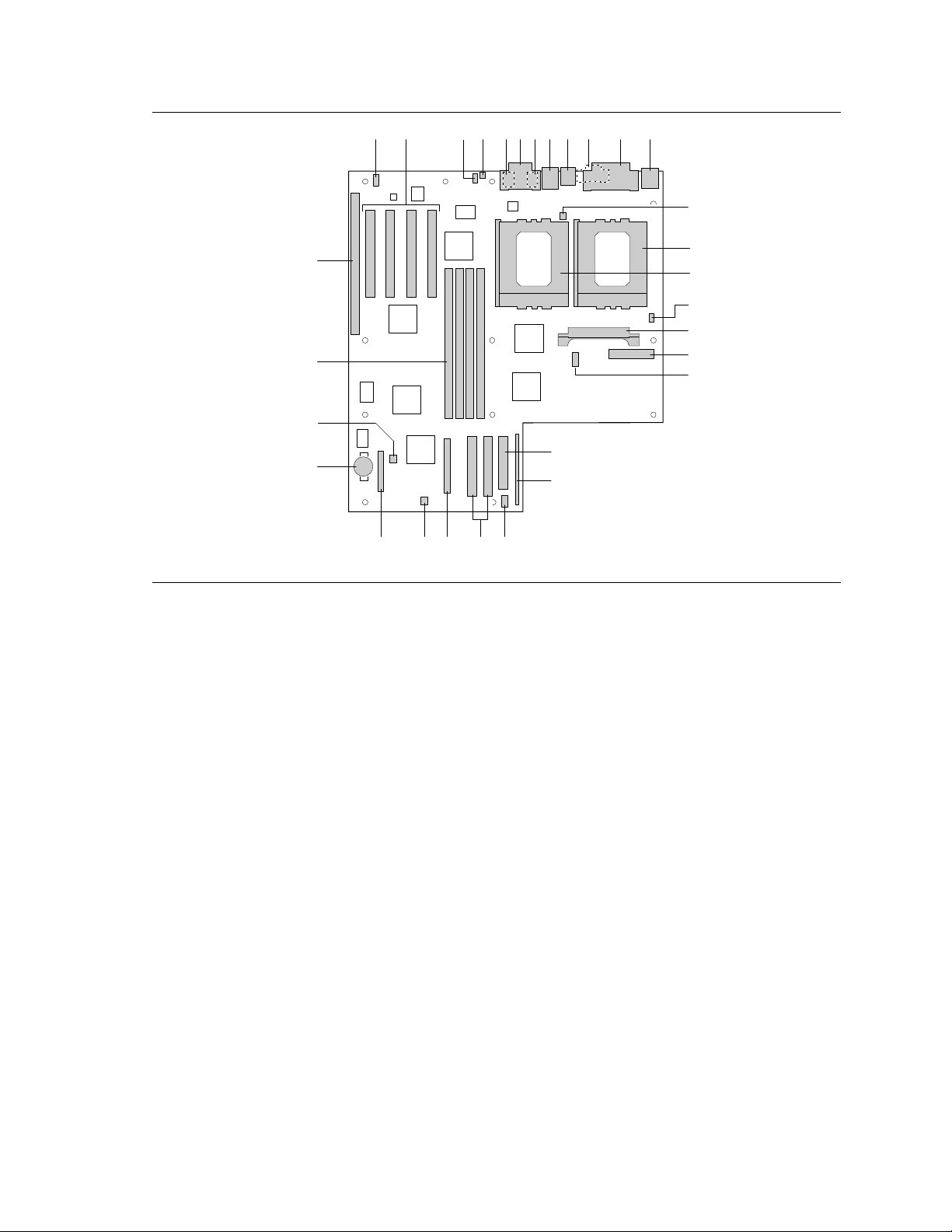
PR440FX Motherboard Technical Product Specification
B
A
C D L
E
F KJG
H
I
M
DD
O
P
Q
N
CC
R
S
BB
T
AA
U
Z
YWX
V
OM04737A
Figure 1. Motherboard Features
A Wavetable connector P Primary processor fan connector
B PCI add-in card connectors Q VRM connector
C CD-ROM audio connector R Power supply connector
D Telephony connector S Serial port 2 header
E Audio connector (Mic In) T Floppy drive connector
F MIDI/Game Port U Front panel I/O header
G Audio connector (Line Out) V SCSI front panel LED connector
H RJ-45 Ethernet connector W PCI IDE connectors
I Dual USB connectors X SCSI connector
J Serial port 1 connector Y Card slot fan connector
K Parallel port connector Z Configuration jumper block
†
L PS/2
M Secondary processor fan connector BB Memory speed jumper block
N Primary processor socket CC DIMM connectors
O Secondary processor socket DD ISA add-in card connector
mouse and PS/2 keyboard AA Battery
8
Page 9
Motherboard Description
OM04737C
3.35
0.65
12.70
11.4
0.30
0.0
0.0
11.35
3.10 4.90
11.10
12.30
6.2
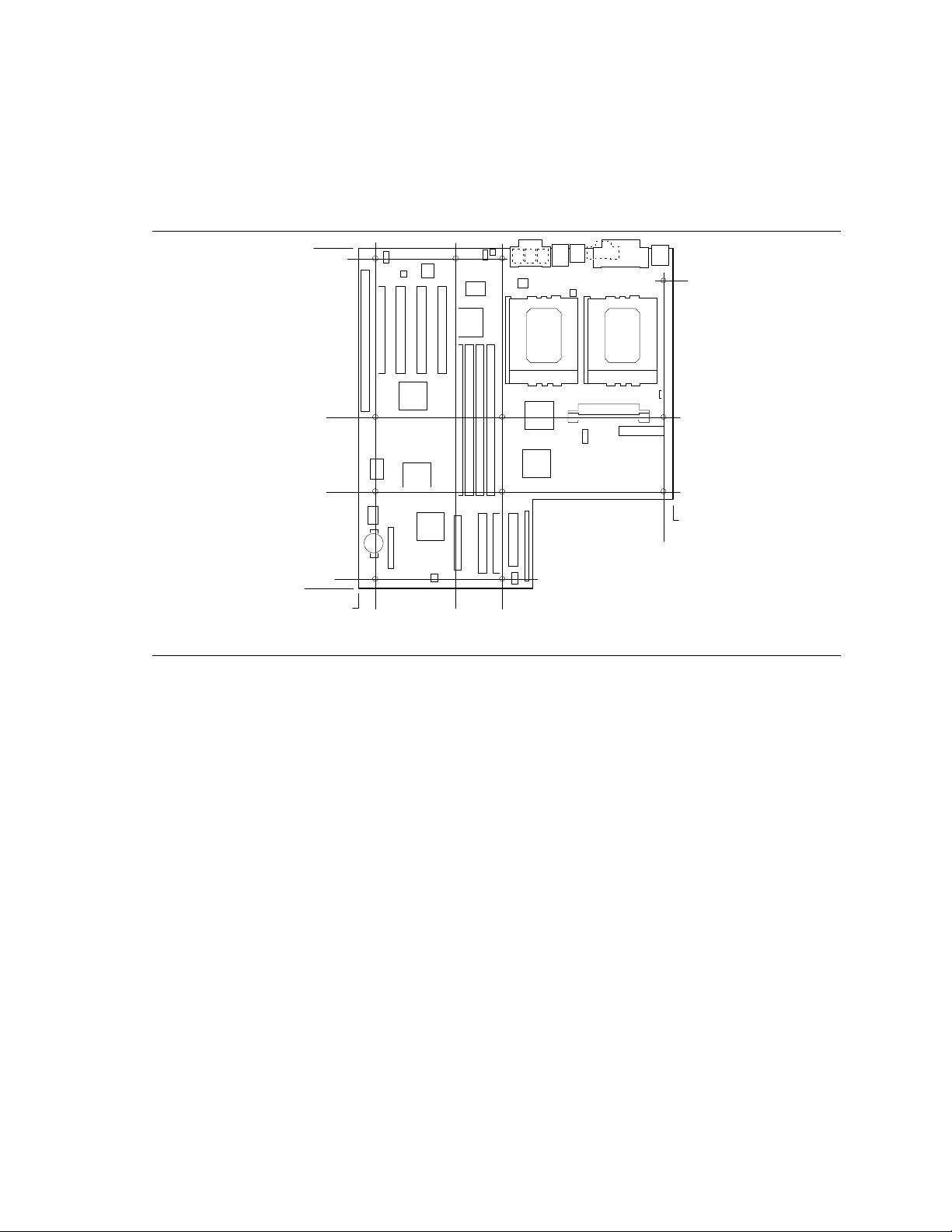
1.2 Custom ATX Form Factor
The PR440FX motherboard is designed to fit into an ATX form factor chassis. Figure 2 illustrates
the mechanical form factor of the motherboard.
Figure 2. Motherboard Dimensions
1.3 Microprocessor
The PR440FX motherboard supports 2.1 V to 3.5 V Intel Pentium Pro processors operating at
180 MHz and 200 MHz. For motherboards with two processors installed, a voltage regulator
module (VRM) is required for the second processor.
The Pentium Pro processor integrates an internal nonblocking second-level (L2) cache and cache
controller. The motherboard supports processors with 256 KB or 512 KB L2 cache.
The Pentium Pro processor maintains full backward compatibility with the 8086, 80286,
™
Intel386
, Intel486™ and Pentium processors. It also has a numeric coprocessor that significantly
increases the speed of floating point operations and complies with ANSI/IEEE standard 754-1985.
9
Page 10
PR440FX Motherboard Technical Product Specification
AAAA
AAAA
AAAA
AAAA
AAAA
AAAA
AAAA
AAAA
AAAA
AAAA
AAAA
AAAA
AAAA
AAAA
AAAA
AAAA
AAAA
AAAA
AAAA
AAAA
AAAA
AAAA
AAAA
AAAA
AAAA
AAAA
AAAA
AA
AAAA
AAAA
AAAA
AAAA
AAAA
AAAA
AAAA
AAAA
AAAA
AAAA
AAAA
AAAA
AAAA
AAAA
AAAA
AAAA
AAAA
AAAA
AAAA
AAAA
AAAA
AAAA
AAAA
AAAA
AAAA
AAAA
AAAA
AA
1.3.1 Dual Processor Support
The dual processor support for the PR440FX motherboard consists of the following:
• Two Socket 8 ZIF processor sockets
• Voltage regulator module (VRM) socket for a VRM, which provides power to the secondary
processor
• BIOS support for either MPS v1.1 or MPS v.1.4 operating systems
1.3.2 Microprocessor Upgrades
Two microprocessor upgrades are available:
• Single to dual processors
• Upgrade from 180 MHz Pentium Pro processor to 200 MHz Pentium Pro processor
CAUTION
The second processor must be the same speed and second-level cache size as the primary
processor. The second processor must also be the same stepping as, or no more than one stepping
higher than, the primary processor.
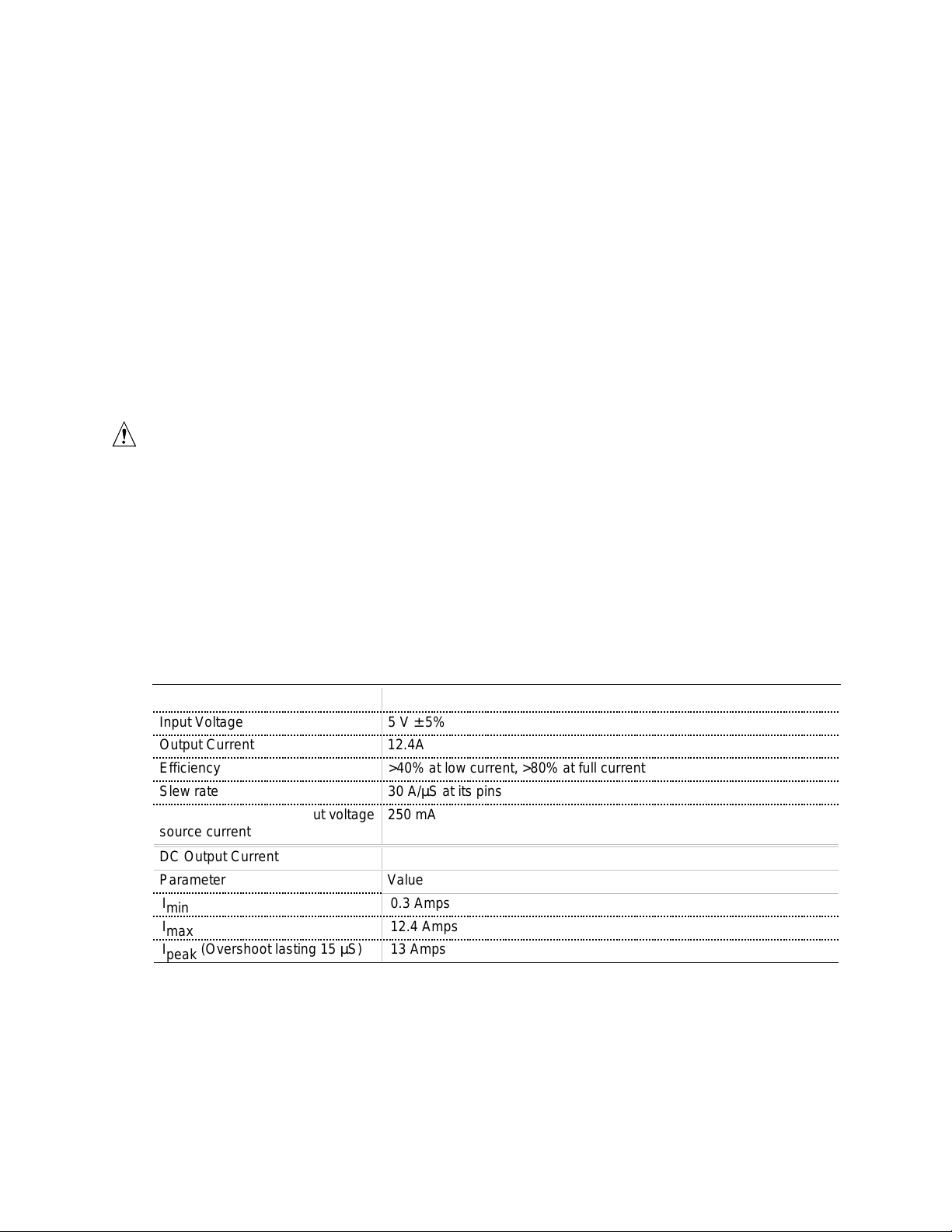
1.3.3 VRM Electrical Characteristics
Motherboards with two processors require a VRM. There are two types of VRMs: 5 V and 12 V.
The PR440FX motherboard supports 5 V modules. Table 1 shows the electrical characteristics of
the VRM.
Table 1. VRM Electrical Characteristics
Parameter Value
Input Voltage 5 V ± 5%
Output Current 12.4A
Efficiency >40% at low current, >80% at full current
Slew rate 30 A/µS at its pins
Maximum secondary input voltage
source current
DC Output Current
Parameter Value
I
min
I
max
I
(Overshoot lasting 15 µS) 13 Amps
peak
250 mA
0.3 Amps
12.4 Amps
10
Page 11

Motherboard Description
Pentium Pro processor-based systems require voltage levels between the minimum and maximum
levels shown in Table 2. The voltage level required by the system depends on the speed of the
Pentium Pro processor. The Icc column represents Intel’s current requirement for a Pentium Pro
processor operating in this voltage range.
Table 2. VRM Voltage Ranges
Voltage Minimum Voltage Maximum Icc
2.4 Volts 3.4 Volts 12.4 Amps
1.3.4 Microprocessor Fan/Heat Sink Assembly and Clips
CAUTION
Do not use the older style of bail-wire clips for securing the fan/heat sink assembly. These clips
could damage the motherboard if installed or removed incorrectly.
In an ATX v. 1.1 compliant chassis, the chassis’s power supply provides the fan for the primary
processor; the primary processor must also have a heat sink for proper thermal dissipation. The
secondary processor must have an active fan/heat sink assembly for proper thermal dissipation.
The heat sink assembly must be securely fastened to the Socket 8 ZIF socket by clips.
1.3.4.1 Secondary Processor Fan
In dual processor systems where both processors have a fan/heat sink assembly, both tach fans
must comply with the specifications in Table 3.
Table 3. Tach Fan Specifications
Parameter Value
Operating voltage range 10.2 - 13.8 VDC
Current (worst case) 80 mA
Air Volume (worst case) at zero pressure 9.9 CFM
Static Pressure (worst case) at zero air flow 0.051 inch H2O
Noise (worst case) 25 dB @ 1 m
Initial RPM (nominal) 2800 ± 600
Size 60 x 60 x 10 mm,
screw centers 50 x 50 mm
Tachometer output 2 cycles per revolution
11
Page 12

PR440FX Motherboard Technical Product Specification
1.4 Memory
1.4.1 Main Memory
The motherboard has four DIMM sockets. Minimum memory size is 16 MB and maximum
memory size is 512 MB. The motherboard supports the following memory types, speeds, and
module sizes:
• 168-pin 3.3 V DIMMs with gold-plated contacts
• 50 ns and 60 ns buffered asynchronous EDO memory
• Parity and ECC memory
• 2 MB x 72 (16 MB), 4 MB x 72 (32 MB), 8 MB x 72 (64 MB) and 16 MB x 72 (128 MB)
modules
NOTE
✏
Parity memory operates in ECC mode unless you disable memory error detection in the BIOS
Setup program (see section 3.14.8.4).
1.5 Chipset
The Intel 82440FX PCIset consists of the 82441FX PCI Bridge and Memory Controller (PMC)
and the 82442FX Data Bus Accelerator (DBX). The Intel 82371SB PCI ISA/IDE Xcelerator
(PIIX3) bridge provides the connection between the ISA and PCI buses.
1.5.1 82441FX PCI Bridge and Memory Controller (PMC) and 82442FX Data Bus Accelerator (DBX)
Two devices from the Intel 82440FX chipset, the PMC and DBX, form the core of the
motherboard design. As the host bridge function between the Pentium Pro processors and PCI I/O
system, these devices maintain proper ordering of operations by trapping synchronization events
and flushing buffers. The PMC also acts as memory controller for the system with the DBX
providing the data path to memory
1.5.1.1 82441FX PCI Bridge and Memory Controller (PMC)
The 82441FX comes in a 208-pin QFP package that features:
• Processor interface control
Up to 66 MHz external bus speed
32-bit addressing
• Integrated DRAM controller
72-bit non-interleaved path to memory with ECC support
ECC is implemented as single-bit error checking and correction and multi-bit error
checking and detection
12
Page 13

Motherboard Description
Support for EDO DRAM
16 MB to 512 MB main memory
• Fully synchronous PCI bus interface
PCI Rev. 2.1 V compliant
Up to 33 MHz bus speed
PCI to DRAM > 100 MBps
• Data Buffering
Processor-to-DRAM and PCI-to-DRAM write data buffering
1.5.1.2 82442FX Data Bus Accelerator (DBX)
The DBX connects to the 64-bit Pentium Pro processor data bus, the 72-bit memory data bus and
the 16-bit PMC private data bus. The DBX works in parallel with the PMC to provide a high
performance memory subsystem for Pentium Pro processor-based systems. The DBX comes in a
208-pin QFP package.
1.5.2 82371SB PCI/ISA IDE Xcelerator (PIIX3)
The PIIX3 provides the interface between the PCI and ISA buses and integrates a dual channel
enhanced IDE interface capable of supporting up to four devices. The PIIX3 comes in a 208-pin
QFP package that features:
†
• PCI-to-AT
• ISA refresh address generation
• Interface between the PCI and ISA buses
• Universal Serial Bus controller
Host/hub controller
• Integrated enhanced IDE interface
Support for up to four devices
Programmed Input/Output (PIO) Mode 4 transfers up to 16 MB/sec
Integrated 8 x 32-bit buffer for bus master PCI IDE burst transfers
Bus master mode
• PCI 2.1 compliance
• Enhanced DMA controller
• Interrupt controller and interrupt steering
• Counters/timers
• SMI (System Management Interrupt) interrupt logic and timer with fast on/off mode
• NMI logic
interrupt mapping circuitry
1.5.3 Universal Serial Bus (USB) Support
NOTE
✏
Computer systems that have an unshielded cable attached to the USB port may not meet FCC
Class B requirements even if no device or a low-speed (sub-channel) USB device is attached to the
cable. Use a shielded cable that meets the requirements for high-speed (fully rated) devices.
13
Page 14

PR440FX Motherboard Technical Product Specification
The motherboard has two USB ports. This permits direct connection of two USB peripherals
without an external hub. If more devices are required, an external hub can be connected to either
port. The motherboard supports the standard Universal Host Controller Interface (UHCI).
Features of the USB include:
• Hot Pluggable
• Self-identifying peripherals
• Automatic mapping of function to driver and configuration
• Support for isochronous and asynchronous transfer types over the same set of wires
• Support for up to 127 physical devices
• Guaranteed bandwidth and low latencies appropriate for telephony, audio, and other
applications
• Error handling and fault recovery mechanisms built into the protocol
1.5.4 IDE Support
The motherboard has two independent high-performance bus-mastering PCI/IDE interfaces capable
of supporting PIO Mode 3, PIO Mode 4, and ATAPI devices. The system BIOS supports Logical
Block Addressing (LBA) and Extended Cylinder Head Sector (ECHS) translation modes. The IDE
device transfer rate and translation mode capability is automatically determined by the system BIOS.
Normally, programmed I/O operations require a substantial amount of processor bandwidth. In
†
true multi-tasking operating systems like Windows NT
, the processor bandwidth freed by using
bus mastering IDE can be used to complete other tasks while disk transfers are occurring. When
used in conjunction with the appropriate driver for the operating system, the IDE interface can
operate as a PCI bus master capable of supporting PIO Mode 4 devices with transfer rates of up to
16 MB/sec.
Detailed information on the PCIset is available in the Intel 82440FX PCIset data sheet.
1.6 I/O Controller
Control for the integrated into a single component, the National Semiconductor PC87308. The
PC87308 is a Plug and Play device that features:
• Two NS16C550-compatible UARTs with send/receive 16-byte FIFO
• Multi-mode bidirectional parallel port
†
Standard mode; IBM
Enhanced Parallel Port (EPP) with BIOS/Driver support
High Speed mode; Extended Capabilities Port (ECP) compatible
• Industry standard floppy controller with 16-byte FIFO (2.88 MB floppy support)
• Integrated real-time clock with century calendar functionality
• Integrated 8042-compatible keyboard controller
and Centronics† compatible
The PC87308 is normally configured automatically by the BIOS, but configuration of these
interfaces is also possible using Setup. The serial ports can support any address configuration.
14
Page 15

Motherboard Description
1.6.1 Floppy Controller
The PC87308 is software compatible with the DP8473 and 82077 floppy disk controllers. The
floppy interface can be configured in Setup for:
• 5¼ inch media
360 KB
1.2 MB
• 3½ inch media
720 KB
1.2 MB (read/write only, no format capability)
1.44 MB
2.88 MB
By default, the Floppy A interface is configured for 1.44 MB and Floppy B is disabled.
Configuring the floppy interface for 1.2 MB, 3½ inch (3-mode floppy) requires a driver.
1.6.2 Keyboard and Mouse Interface
PS/2 keyboard/mouse connectors are located on the back panel side of the motherboard. The 5 V
lines to these connectors are protected with a PolySwitch
healing fuse, re-establishing the connection after an over-current condition is removed. While this
device eliminates the possibility of having to replace a fuse, take care to turn off the system power
before installing or removing a keyboard or mouse.
The I/O controller contains the AMI Megakey keyboard/mouse controller code which, besides
providing traditional keyboard and mouse control functions, supports Power-On/Reset (POR) and
password protection. You can define the POR password with Setup. The keyboard controller also
provides for the following hot-key sequences:
• <Ctrl> <Alt> <Del>: System software reset. This sequence performs a software reset of the
system by jumping to the beginning of the BIOS code and running the POST operation.
• <Ctrl> <Alt> <defined in Setup>: Power management key sequences take advantage of the
processor’s System Management Mode (SMM) features to greatly reduce the system’s power
consumption while maintaining the responsiveness necessary to service external interrupts.
• <Ctrl> <Alt> <defined in Setup>: Keyboard secure hot keys lock the keyboard until you enter
the password.
†
circuit which acts much like a self-
1.6.3 Real Time Clock, CMOS RAM and Battery
The integrated real-time clock (RTC) is compatible with DS1287 and MC146818 components. It
provides a time of day clock, a 100-year calendar with alarm features, and a century register. You
can set RTC in Setup. The RTC also supports 256-byte battery-backed CMOS RAM in two banks
which is reserved for BIOS use. You can set the CMOS RAM to specific values or clear the
CMOS RAM to system default values using Setup. You can also clear the CMOS RAM values to
system defaults by using a configuration jumper on the motherboard.
An external coin-cell style battery provides power to the RTC and CMOS memory. The battery
has an estimated lifetime of seven years and is socketed for easy replacement. When the system is
on, the life of the battery is extended by a trickle current from the power supply.
15
Page 16
PR440FX Motherboard Technical Product Specification
1.6.4 Parallel Port
A 25-pin D-Sub header is provided on the back panel for a multi-mode bidirectional parallel port.
The parallel port operates in standard mode, EPP version 1.7 mode (BIOS and driver support) or a
high speed ECP compatible mode. EPP Mode requires a driver provided by the peripheral
manufacturer to operate correctly.
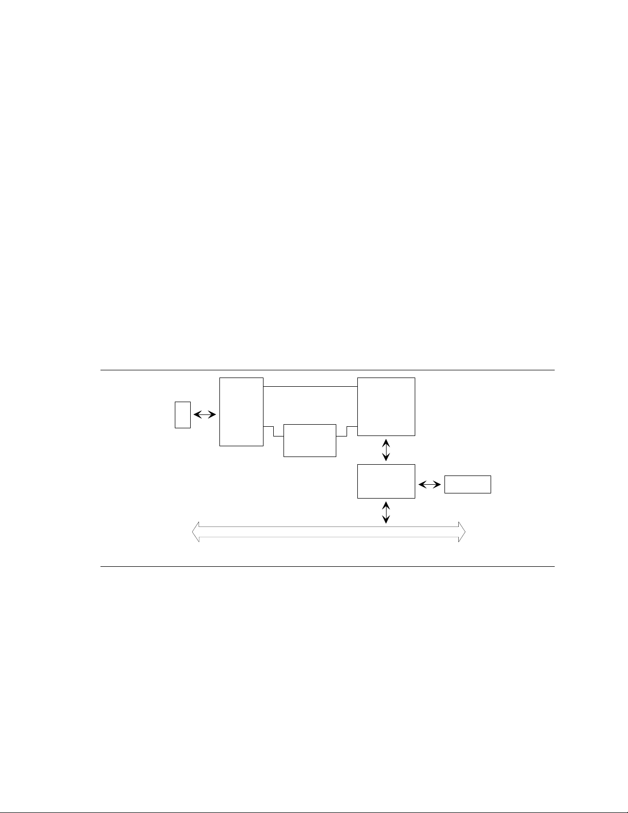
1.7 Onboard Networking
1.7.1 EtherExpress™ PRO/100B PCI LAN Subsystem
The EtherExpress PRO/100B PCI LAN optional subsystem is a high performance Ethernet† LAN
interface that provides both 10Base-T and 100Base-TX connectivity. Features include:
• 32-bit direct bus mastering on the PCI bus
• Shared memory structure in the host memory that copies data directly to/from host memory
• 10Base-T and 100Base-TX capability using a single RJ-45 connector
• IEEE 802.3µ Auto-Negotiation for hardware selection of the highest operating speed
• Jumperless configuration; the LAN subsystem is totally software configurable
The following block diagram provides an overview of the LAN subsystem architecture.
10Mbps Xmit/Rcv
RJ-45
Connector
Common
Magnetic
Module
100Mbps Xmit/Rcv
DP8322 3
"Twister"
PCI Local Bus
DP83840
100BASE-TX
PHY
MII
Intel
82557
Figure 3. Functional Block Diagram of LAN Subsystem
1.7.2 Intel 82557 LAN Controller
This device is the heart of the LAN subsystem and provides the following functions:
• CSMA/CD Protocol Engine
• PCI bus interface
• DMA engine for movement of commands, status, and network data across the PCI bus
• Access to EEPROM
• Standard MII interface for access to IEEE 802.3µ-compliant physical layer devices
EEPRO M
OM04782
16
Page 17

Motherboard Description
1.7.3 10/100 MBps Physical Layer Interface
The physical layer interface is implemented in two devices from National Semiconductor, the
DP83840 and the DP83223. The DP83840 provides:
• Complete functionality necessary for the 10Base-T interface; directly drives the cable when in
10 MBps mode
• All functionality required for the 100Base-TX interface except for the NRZ to MLT3
encoding/decoding function, which is provided by the DP83223 Twister device
• Complete set of MII management registers for control and status reporting
• 802.3µ Auto-Negotiation for automatically establishing the best possible operating mode when
connected to other 10Base-T or 100Base-TX devices, whether capable of half or full-duplex
operation
1.7.4 EtherExpress PRO/100B PCI LAN Subsystem Software Description
The software provided with the LAN subsystem includes setup/diagnostic software (SETUP.EXE),
a readme file viewer (README.EXE) and the following drivers:
Table 4. EtherExpress PRP/100B PCI Drivers
Driver Description Environment(s)
E100BODI.COM Novell ODI NetWare† DOS Client
E100BODI.SYS Novell ODI NetWare OS/2† Client
E100B.LAN Novell ODI NetWare 3.11 Server
NetWare 3.12 Server
NetWare 4.x Server
NetWare NT Requester
NetWare for OS/2
†
E100B.DOS NDIS 2.0.1 Windows
MS-DOS
E100B.OS2 NDIS 2.0.1 MS OS/2 1.3
IBM OS/2 2.11
IBM OS/2 Warp
E100B.SYS NDIS 3.1 Windows 95
Windows NT 3.5x
for Workgroups 3.11
†
LANMAN 2.1
1.8 SCSI Subsystem
The onboard SCSI subsystem features the Adaptec AIC-7880, which contains a double-speed SCSI
controller and a PCI bus master interface in a 160-pin PQFP. The AIC-7880 supports the
following:
• 8- or 16-bit fast SCSI providing 10 MB per second or 20 MB per second throughput, or
• Double-speed SCSI that can burst data at 20 MB per second or 40 MB per second
As a PCI bus master, the AIC-7880 supports burst data transfers on the PCI bus up to the
maximum rate of 133 MB per second using the on-chip 256-byte FIFO.
17
Page 18
PR440FX Motherboard Technical Product Specification
1.8.1 SCSI Interface
The AIC 7880 also offers active negation outputs and a disk activity output signal. Active
negation outputs reduce the chance of data errors by actively driving both polarities of the SCSI
bus, avoiding indeterminate voltage levels and common-mode noise on long cable runs. The SCSI
output drivers can directly drive a 48 mA single-ended SCSI bus with no additional drivers.
Synchronous SCSI can handle up to 15 REQ control signals simultaneously.
1.8.2 SCSI Bus
The SCSI data bus is 8- or 16-bits wide with odd ECC generated per byte. SCSI control signals
are the same for either bus width. The motherboard has an onboard SCSI connector that supports
8- or 16-bit devices. On a 16-bit wide SCSI bus, the AIC-7880 assigns the highest arbitration
priority to the low byte of the 16-bit word. This way, 16-bit targets can be mixed with 8-bit targets
if the 8-bit devices are placed on the low data byte. During chip powerdown, all inputs are
disabled to reduce power consumption.
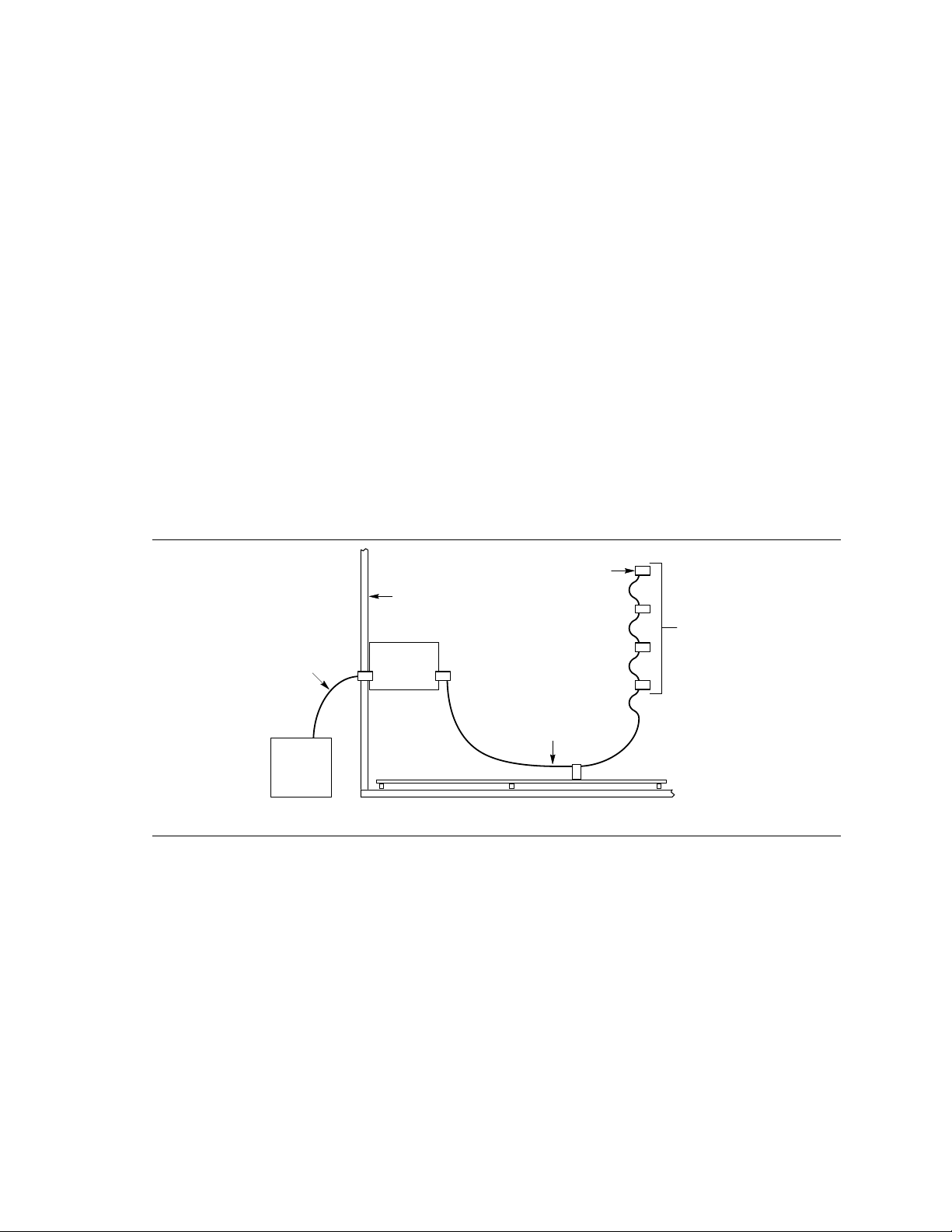
1.8.2.1 SCSI Bus Topology
The following diagram shows how the SCSI bus is implemented.
Last
Internal
Device
Internal
SCSI
Devices
Internal
SCSI
Cable
OM05664a
External
SCSI
Cable
External
SCSI
Device
Chassis
Terminator
Card
Motherboard
Figure 4. SCSI Bus Topology
From end to end, the SCSI bus cable is routed from the last internal SCSI device to each internal
device. From the last internal device, the cable connects to the motherboard, where the SCSI
controller resides. The cable can then continue to an optional terminator card installed in an
unused I/O slot of the chassis. From the terminator card, an optional external SCSI cable can be
used to connect external SCSI devices.
18
Page 19

Motherboard Description
1.8.3 SCSI Cable
For proper operation of ultra/wide SCSI devices, the overall length of the SCSI cable from the last
internal device to the last external device should not exceed three meters (within constraints as
defined by ANSI SCSI-3 Specification). The recommended length for the internal SCSI cable
(from the last internal device to the terminator card) is 42 inches. For more information, see the
ANSI SCSI-3 Specification.
1.8.4 SCSI Bus Termination
Terminate the extreme ends of the SCSI bus (cable), typically by connecting a terminated device to
the end connectors of the cable:
• On the last connector of the internal cable (farthest from the motherboard), attach either a
terminated 16-bit device or some other type of 16-bit termination (see Note).
• If the internal cable ends at the motherboard, enable motherboard termination in the SCSI
BIOS (on bootup press <Ctrl><A> to enter the SCSISelect
• If the internal cable continues from the motherboard to a termination card, disable motherboard
termination in the SCSI BIOS (using SCSISelect). The terminator card provides the end
termination, unless you attach an external cable.
• If an external SCSI cable is attached to the terminator card, its termination is disabled
automatically. On the last connector of the external cable, attach either a terminated 16-bit
device or some other type of 16-bit termination (see Note).
†
utility).
Disable termination on all other SCSI devices attached to the cable (except the devices attached to
the extreme ends).
NOTE
✏
A 68-pin connector on the motherboard supports 8-bit and wide 16-bit SCSI devices. Eight-bit
devices require a 68- to 50-pin adapter. In general, if you use an 8-bit device to terminate the
SCSI bus, you must attach it using a 68-to-50-pin SCSI adapter with high-byte termination, so that
all 16 data bits are terminated.
1.8.4.1 Using Only 16-bit SCSI Devices
• Enable termination only on the device(s) attached to the last connector (internal and/or
external).
• Remove or disable termination on all devices that are not on the last connector of the cable(s).
1.8.4.2 Mixing 8-and 16-bit SCSI Devices
• When mixing 8- and 16-bit devices, each 8-bit device must have a 68-to-50 pin adapter.
• Enable termination only on the device(s) attached to the last connector (internal and/or
external). If you use an 8-bit device to provide termination, attach it using a 68-to-50-pin SCSI
adapter with high-byte termination, so that all 16 data bits are terminated.
• Remove or disable termination on all devices that are not on the last connector of the cable(s).
19
Page 20

PR440FX Motherboard Technical Product Specification
1.8.4.3 Using Only 8-bit SCSI Devices
• Enable termination only on the device(s) attached to the last connector (internal and/or
external). Attach the 8-bit device to provide termination using a 68-to-50-pin SCSI adapter
with high-byte termination, so that all 16 data bits are terminated.
• Remove or disable termination on all devices that are not the last device on the cable(s).
NOTE
✏
Examine the gender and polarities of connectors, adapters, and terminators to assure proper
termination and connection to the low or high byte of the bus.
1.8.5 SCSI
See Section 4.0.
Select
and SCSI Disk Utilities
1.9 Audio Subsystem
The motherboard features a 16-bit stereo audio subsystem. The audio subsystem is based upon the
Sound Blaster
audio and analog mixing functions required for playing and recording audio on personal computers
including:
• Stereo analog-to-digital and digital-to-analog converters
• Analog mixing, anti-aliasing and reconstruction filters
• Line and microphone level inputs
• Digital audio compression using selectable A-law or µlaw rules
• Full digital control of all mixer and volume control functions
With the integrated Sound Blaster OPL3 compatible FM synthesizer, the CS4236 also provides
support for four major sound standards including Adlib and Sound Blaster Pro 2.0, Windows
Sound System and MPU-401 to meet all of the requirements of today’s multimedia applications.
The CS4236 also supports full-duplex operation to support future applications such as video
conferencing.
The CS4236 includes a Plug and Play ISA interface and comprises six logical devices including:
• Synthesizer
• MIDI/Game Port
• Sound Blaster
• Microsoft
• MPU-401
• CS4236 device
†
compatible Crystal CS4236 multimedia codec. The CS4236 provides the digital
†
Sound System
Each logical device is configured into the host environment using ISA Plug and Play configuration.
The audio subsystem requires two interrupts and up to two DMA channels. The system can be
configured to use either DMA channels 0, 1, or 3. The interrupt can be mapped to interrupt 5, 7, 9,
10, 11, or 15.
20
Page 21

Motherboard Description
Address (hex)
80h
85h
86h
1.10 Management Extension Hardware
The Management Extension hardware provides low-cost instrumentation capabilities. The
hardware implementation is a single-chip ASIC. Features include the following:
• An integrated temperature sensor for internal chassis temperature
• Three fan-speed sensors
• Power supply voltage monitoring to detect levels above or below acceptable values
• Registers for storing power on self test (POST) hardware test results and error codes
• Optical sensor for detection of physical intrusion (such as when the chassis lid has been
removed) even when the power is off (this feature is chassis dependent)
• Remote reset capabilities from a remote peer or server through LANDesk Client Manager,
Version 3.0 and service layers (when available)
• Hardware compatibility with Windows NT, Windows 95, and Windows† 3.1
When an out-of-range condition (temperature, fan speed, or voltage) is reached, a System
Management Interrupt (SMI) is activated. The Management Extension circuitry connects to the
ISA bus as an 8-bit I/O mapped device and uses these I/O addresses:
Description
Monitors and stores POST codes
Address and control functions
Register read/write operations
21
Page 22
PR440FX Motherboard Technical Product Specification
1.11 Motherboard Connectors
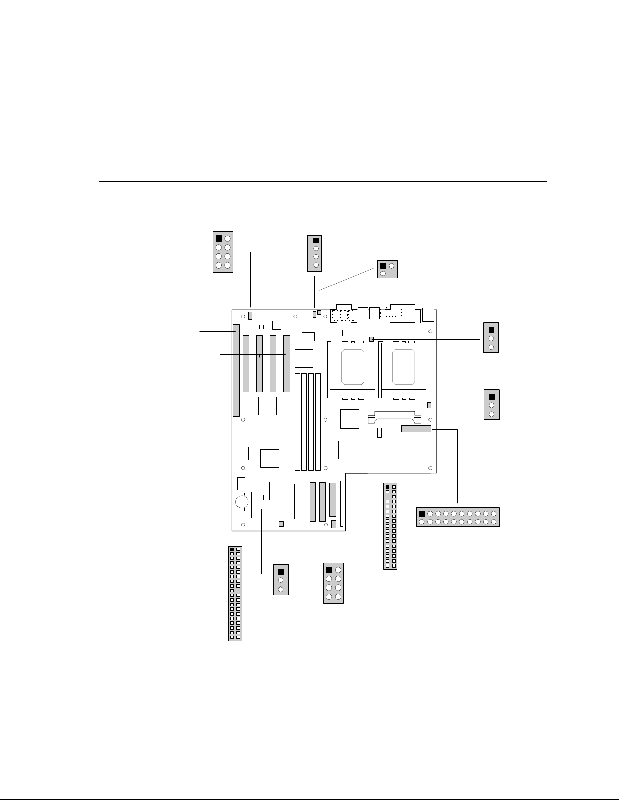
Figure 5 shows the connectors on the motherboard. Following figure 5 are the pins and signal
names for each connector. For front panel connectors, see section 1.12. For back panel
connectors, see section 1.13.
J1B1
1
2
87
Wave
Table
J1E1
1
4
CD-ROM
Audio
1
Telephony
J1F1
J4A1
ISA
PCI #1 - J4A2
PCI #2 - J4B1
PCI #3 - J4C1
PCI #4 - J4D1
PCI IDE(2)
Secondary - J12E1
Primary - J12F1
39
J2J1
1
3
CPU2 Fan
J6M1
1
3
CPU1 Fan
1
2
5
Floppy
Drive
1
J12F2
2
1
J13C1
Card Slot
Fan
40
1
3
J13G1
1
SCSI
Hard Drive
Front Panel
LED
33
2
87
34
J8L1
20
Power
OM04737E
22
Figure 5. Motherboard Connectors
continued ☛
Page 23
Motherboard Description
J7K1
2
21
40
DIMM #1 DIMM #2 DIMM #3 DIMM #4 -
J12D1
1
J7D2
J7E1
J7E2
J7F1
1
VRM
39
J8J1
12
9
8
COM 2
Header
SCSI
Figure 5. Motherboard Connectors (continued)
1.11.1 CD-ROM Connector - J1E1
Pin Signal Name
1 Ground
2 CD-Left
3 Ground
4 CD-Right
OM05882
23
Page 24

PR440FX Motherboard Technical Product Specification
1.11.2 Wavetable Connector - J1B1
Pin Signal Name
1 Wave Right
2 Ground
3 Wave Left
4 Ground
5 Key
6 Ground
7 N/C
8 MIDI-Out
1.11.3 Telephony Connector - J1F1
Pin Signal Name
1 Ground
2 Mono Out
3 Mic In
4 Key
1.11.4 Power Connector - J8L1
When used with a power supply that supports Remote On/Off, the motherboard can turn off the
system power under software control. The BIOS turns the computer power off when it receives the
proper APM command from the operating system. For example, Windows 95 issues an APM
command when the user selects the Shutdown the Computer option. APM must be enabled in the
BIOS and the operating system in order for Soft Off to work correctly. APM determines the status
of the power supply system responses. For example, if the power is disconnected and computer is
switched on, the computer’s response is to either turn back on when power is reapplied or remain
off. The response is predetermined by the configuration in Setup. Also see 1.12.1.4 Remote
On/Off and Soft Power Support.
Pin Signal Name Pin Signal Name
1 +3.3V 11 +3.3V
2 +3.3V 12 -12V
3 Ground 13 Ground
4 +5V 14 PS-ON
5 Ground 15 Ground
6 +5V 16 Ground
7 Ground 17 Ground
8 PW-OK 18 -5V
9 +5VSB 19 +5
10 +12V 20 +5V
24
Page 25

1.11.5 Floppy Drive Connector - J12F2
Pin Signal Name Pin Signal Name
1 Ground 2 DENSEL
3 Ground 4 Reserved
5 Key 6 FDEDIN
7 Ground 8 Index#
9 Ground 10 Motor Enable A#
11 Ground 12 Drive Select B#
13 Ground 14 Drive Select A#
15 Ground 16 Motor Enable B#
17 MSEN1 18 DIR#
19 Ground 20 STEP#
21 Ground 22 Write Data#
23 Ground 24 Write Gate#
25 Ground 26 Track 00#
27 MSEN0 28 Write Protect#
29 Ground 30 Read Data#
31 Ground 32 Side 1 Select#
33 Ground 34 Diskette Change#
Motherboard Description
1.11.6 IDE Connectors - J12E1, J12F1
Pin Signal Name Pin Signal Name
1 Reset IDE 2 Ground
3 Host Data 7 4 Host Data 8
5 Host Data 6 6 Host Data 9
7 Host Data 5 8 Host Data 10
9 Host Data 4 10 Host Data 11
11 Host Data 3 12 Host Data 12
13 Host Data 2 14 Host Data 13
15 Host Data 1 16 Host Data 14
17 Host Data 0 18 Host Data 15
19 Ground 20 Key
21 DDRQ0 [DDRQ1] 22 Ground
23 I/O Write# 24 Ground
25 I/O Read# 26 Ground
27 IOCHRDY 28 Vcc pull-up
29 DDACK0# [DDACK1#] 30 Ground
31 IRQ14 (IRQ15) 32 Reserved
continued
☛
25
Page 26

PR440FX Motherboard Technical Product Specification
IDE Connectors (continued)
Pin Signal Name Pin Signal Name
33 Addr 1 34 Reserved
35 Addr 0 36 Addr 2
37 Chip Select 1P#
[Chip Select 1S#]
39 Activity# 40 Ground
[ ] Indicates secondary IDE connector
38 Chip Select 3P#
1.11.7 ISA Connectors - J4A1
Pin Signal Name Pin Signal Name
B1 GND A1 IOCHK#
B2 RSTDRV A2 SD7
B3 Vcc A3 SD6
B4 IRQ9 A4 SD5
B5 -5 V A5 SD4
B6 DRQ2 A6 SD3
B7 -12 V A7 SD2
B8 0WS# A8 SD1
B9 +12 V A9 SD0
B10 GND A10 IOCHRDY
B11 SMEMW# A11 AEN
B12 SMEMR# A12 SA19
B13 IOW# A13 SA18
B14 IOR# A14 SA17
B15 DACK3# A15 SA16
B16 DRQ3 A16 SA15
B17 DACK1# A17 SA14
B18 DRQ1 A18 SA13
B19 REFRESH# A19 SA12
B20 SYSCLK A20 SA11
B21 IRQ7 A21 SA10
B22 IRQ6 A22 SA9
B23 IRQ5 A23 SA8
B24 IRQ4 A24 SA7
B25 IRQ3 A25 SA6
B26 DACK2# A26 SA5
B27 TC A27 SA4
B28 BALE A28 SA3
[Chip Select 3S#]
26
continued
☛
Page 27

Motherboard Description
Pin
A1
A2
A3
A4
A5
A6
A7
A8
A9
A10
A11
A12
ISA Connectors J4A1 (continued)
Pin Signal Name Pin Signal Name
B29 Vcc A29 SA2
B30 OSC A30 SA1
B31 GND A31 SA0
KEY KEY
D1 MEMCS16# C1 SBHE#
D2 IOCS16# C2 LA23
D3 IRQ10 C3 LA22
D4 IRQ11 C4 LA21
D5 IRQ12 C5 LA20
D6 IRQ15 C6 LA19
D7 IRQ14 C7 LA18
D8 DACK0# C8 LA17
D9 DRQ0 C9 MEMR#
D10 DACK5# C10 MEMW#
D11 DRQ5 C11 SD8
D12 DACK6# C12 SD9
D13 DRQ6 C13 SD10
D14 DACK7# C14 SD11
D15 DRQ7 C15 SD12
D16 Vcc C16 SD13
D17 Master# C17 SD14
D18 GND C18 SD15
1.11.8 PCI Connectors - J4A2, J4B1, J4C1, J4D1
Signal Name Pin Signal Name Pin Signal Name Pin Signal Name
TRST#* B1 -12 V A32 AD16 B32 AD17
+12 V B2 TCK A33 3.3 V B33 CBE2#
TMS (TMS)** B3 GND A34 FRAME# B34 GND
TDI** B4 TDO (NC) A35 GND B35 IRDY#
Vcc B5 Vcc A36 TRDY# B36 3.3 V
INTA# [INT1] B6 Vcc A37 GND B37 DEVSEL#
INTC# [INT3] B7 INTB# [INT2] A38 STOP# B38 GND
Vcc B8 INTD# [INT4] A39 3.3 V B39 LOCK#
Reserved B9 Prsnt1# A40 SDONE B40 PERR#
Vcc B10 Reserved A41 SBO# B41 3.3 V
Reserved B11 Prsnt2# A42 GND B42 SERR#
GND B12 GND A43 PAR B43 3.3 V
continued
☛
27
Page 28

PR440FX Motherboard Technical Product Specification
Pin
A13
A14
A15
A16
A17
A18
A19
A20
A21
A22
A23
A24
A25
A26
A27
A28
A29
A30
A31
PCI Connectors (continued)
Signal Name Pin Signal Name Pin Signal Name Pin Signal Name
GND B13 GND A44 AD15 B44 CBE1#
Reserved B14 Reserved A45 3.3 V B45 AD14
RST# B15 GND A46 AD13 B46 GND
Vcc B16 CLK A47 AD11 B47 AD12
GNT# B17 GND A48 GND B48 AD10
GND B18 REQ# A49 AD9 B49 GND
Reserved B19 Vcc A50 KEY B50 KEY
AD30 B20 AD31 A51 KEY B51 KEY
3.3 V B21 AD29 A52 CBEO# B52 AD8
AD28 B22 GND A53 3.3 V B53 AD7
AD26 B23 AD27 A54 AD6 B54 3.3 V
GND B24 AD25 A55 AD4 B55 AD5
AD24 B25 3.3 V A56 GND B56 AD3
IDSEL B26 CBE3# A57 AD2 B57 GND
3.3 V B27 AD23 A58 AD0 B58 AD1
AD22 B28 GND A59 Vcc B59 Vcc
AD20 B29 AD21 A60 REQ64# B60 ACK64#
GND B30 AD19 A61 Vcc B61 Vcc
AD18 B31 3.3 V A62 Vcc B62 Vcc
* Pulled down to a logic low.
** Pulled up to a logic high.
NOTE
✏
The shared PCI slot (J4A2) does not support bus mastering.
1.11.9 Primary Processor Fan Connector - J6M1
Pin Signal Name
1 GND
2 +12 V
3 P60_FAN (fan tachometer)
1.11.10 Secondary Processor Fan Connector - J2J1
Pin Signal Name
1 GND
2 +12 V
3 P61_FAN (fan tachometer)
28
Page 29

Motherboard Description
1.11.11 Card Slot Fan Connector - J13C1
Pin Signal Name
1 GND
2 +12 V
3 SLOT_FAN (fan tachometer)
1.11.12 SCSI Hard Drive Front Panel LED Connector LED - J13G1
Pin Signal Name* Pin Signal Name*
1 No connect 2 No connect
3 HDACT# 4 HDACT#
5 HDACT# 6 HDACT#
7 No connect 8 No connect
* The signals in this table are all input signals
1.11.13 VRM Connector - J7K1
Signal Name
Pin
(Row A) Pin
1 Vcc 2 Vcc
3 Vcc 4 Vcc
5 Vcc 6 Vcc
7 +12 V in 8 +12 Vin
9 Reserved 10 Reserved
11 Reserved 12 OUTEN
13 VID0 14 VID1
15 VID2 16 VID3
17 UP# 18 PWRGD
19 Vccp 20 Vss
21 Vss 22 Vccp
23 Vccp 24 Vss
25 Vss 26 Vccp
27 Vccp 28 Vss
29 Vss 30 Vccp
31 Vccp 32 Vss
33 Vss 34 Vccp
35 Vccp 36 Vss
37 Vss 38 Vccp
39 Vccp 40 Vss
Signal Name
(Row B)
29
Page 30

PR440FX Motherboard Technical Product Specification
Pin
1
2
3
4
5
6
7
8
9
10
11
12
13
14
15
16
17
18
1.11.14 Serial Port 2 Header - J8J1
Pin Signal Name
1 DCD#
2 DSR#
3 SIN#
4 RTS#
5 SOUT#
6 CTS#
7 DTR#
8RI
9 GND
10 Key
1.11.15 SCSI Connector - J12D1
Signal Name Pin Signal Name Pin Signal Name Pin Signal Name
GND 19 N/C 37 SCSI_D14 55 SCSI_ATN#
GND 20 GND 38 SCSI_D15 56 GND
GND 21 GND 39 SCSI_DPH# 57 SCSI_BSY#
GND 22 GND 40 SCSI_D0 58 SCSI_ACK#
GND 23 GND 41 SCSI_D1 59 SCSI_RST#
GND 24 GND 42 SCSI_D2 60 SCSI_MSG#
GND 25 GND 43 SCSI_D3 61 SCSI_SEL#
GND 26 GND 44 SCSI_D4 62 SCSI_CD#
GND 27 GND 45 SCSI_D5 63 SCSI_REQ
GND 28 GND 46 SCSI_D6 64 SCSI_IO#
GND 29 GND 47 SCSI_D7 65 SCSI_D8
GND 30 GND 48 SCSI_DPL# 66 SCSI_D9
GND 31 GND 49 GND 67 SCSI_D10
GND 32 GND 50 GND 68 SCSI_D11
GND 33 GND 51 TERM_PWR
GND 34 GND 52 TERM_PWR
TERM_PWR 35 SCSI_D12 53 N/C
TERM_PWR 36 SCSI_D13 54 GND
30
Page 31

Motherboard Description
Front Panel
I/O Header
J12G1
OM05883
27
1
Speaker
HDD LED
Reserved
Reset
Powe r LED
Sleep
Power
1.12 Front Panel Connectors
The motherboard has header connectors to support controls and indicators typically located on the
chassis bezel including:
• Power switch
• Power LED
• Sleep switch
• Hard drive activity LED
• Reset switch
• Speaker
Figure 6 shows the location of the front panel connectors on the motherboard. Following figure 6
are the pins and signal names for each connector.
Figure 6. Front Panel Connectors
31
Page 32

PR440FX Motherboard Technical Product Specification
Pin
1
AAAA
AAAA
AAAA
AAAA
AAAA
AAAA
AAAA
AAAA
AAAA
2
AAAA
AAAA
AAAA
AAAA
AAAA
AAAA
AAAA
AAAA
AAAA
3
4
5
6
7
8
9
AAAA
AAAA
AAAA
AAAA
AAAA
AAAA
AAAA
AAAA
AAAA
10
AAAA
AAAA
AAAA
AAAA
AAAA
AAAA
AAAA
AAAA
AAAA
11
12
13
14
1.12.1 Front Panel Connectors - J12G1
Signal Name Pin Signal Name
Power On (SW_ON) 15 HD ACTIVE#
Power Return 16 +5V
Sleep Req 17 Key
+5V (Sleep Driver) 18 Ground
Key 19 Key
+5V 20 +5V (LED_PWR)
Key 21 Key
Reserved 22 Ground
Ground 23 Reset
Reserved 24 Ground
Reserved 25 Key
Key 26 SPKR_DATA onboard
+5V 27 SPKR_DATA out
Key
1.12.1.1 System Reset
You can connect this header to a momentary SPST type switch that is normally open. When the
switch is closed, the board resets, and runs the POST.
1.12.1.2 Speaker
The external speaker provides error beep code information during the Power-On Self Test, if the
system cannot use the video interface.
1.12.1.3 Sleep / Resume
When advanced power management (APM) is activated in the system BIOS and the Operating
System’s APM driver is loaded, the system can enter Sleep (Standby) in one of three ways:
• Optional front panel Sleep/Resume button
• Hot key (defined in Setup), or mouse button (if mouse driver loaded)
• Prolonged system inactivity; the default is 10 minutes and can be changed in Setup
The Sleep/Resume button is supported by a 2-pin header located on the front panel I/O connector.
The front panel Sleep switch is a momentary two pin SPST type that is normally open.
Closing the Sleep switch generates an SMI (System Management Interrupt) to the processor which
immediately goes into System Management Mode (SMM). While the system is in Sleep mode it is
fully capable of responding to and servicing external interrupts (such as incoming FAX) even
though the monitor turns on only if a keyboard or mouse interrupt occurs. To reactivate the
system, or “Resume,” you must press the sleep / resume button again, or use the keyboard or PS/2
mouse.
32
Page 33

Motherboard Description
1.12.1.4 Remote On/Off and Soft Power Support
For power supplies that support the Remote On/Off feature, pins 1 and 2 of the front panel
connectors (see Figure 6, pins 1 and 2 of J12G1) should be connected to the system power On/Off
switch. The power On/Off button should be a momentary SPST switch that is normally open. The
power supply control signal (SW_ON) is supported by the primary power connector. Traditional
power supplies with mechanical On/Off switches that do not support Remote On/Off or Soft Off
by-pass this circuit.
After turning the system on by pushing the power On/Off button, the motherboard (with a power
supply that supports Remote On/Off) can be turned off from one of two sources:
• Front panel power On/Off switch
• Soft Off signal (coming from the I/O controller)
Soft Off signal can be controlled by the operating system. In Soft Off, an APM command issued
to the system BIOS causes the power supply to turn off with the SW_ON control signal on the
power connector.
33
Page 34

PR440FX Motherboard Technical Product Specification
1.13 Back Panel I/O Connectors
The motherboard has PS/2 style keyboard and mouse connectors, two USB connectors, one RJ-45
LAN connector, one serial port connector, one parallel port connector, one MIDI/Gameport
connector, and Line In, Line Out, and Mic In audio jacks. Figure 7 shows the location of the
connectors.
PS/2
Mouse
PS/2
Keyboard
RJ-45
ENET/LED
MIDI/Game PortPara l le l Po rt
COM 1
USB
Connectors
Line Out
Line In
Figure 7. Back Panel I/O Connectors
Mic In
OM04737D
34
Page 35

1.14 Jumper Settings
OM04737B
H
G
F
E
DC
B
A
J12B1
Configuration
Jumper Bloc k
Up
Down
1
J12 B2
Memory
Speed
3
M
Figure 8 shows the location of jumper blocks on the motherboard.
Motherboard Description
Figure 8. Jumper Block Locations
35
Page 36

PR440FX Motherboard Technical Product Specification
Function
Setup access
Flash mode
CMOS settings
Password
Processor clock
speed
DIMM speed
Table 5. Configuration Jumpers
Jumper Block Jumper Setting
J12B1-A DownUpAccess allowed (Default)
Access denied
J12B1-B DownUpNormal (Default)
Recover
J12B1-C DownUpKeep (Default)
Clear
J12B1-D DownUpPassword enabled (Default)
Password clear / function disabled
J12B1-E through
J12B1-H
J12B2-M See Table 7
See Table 6
1.14.1 Setup Access (J12B1-A)
You can disable access to Setup by moving this jumper from the down position to the up position.
Default access is the down position (access allowed).
1.14.2 Flash Mode (J12B1-B)
You can recover Flash mode by moving the jumper from the down position to the up position. The
default for Flash mode is the down position (normal). For additional information, See Section 3.
1.14.3 CMOS Settings (J12B1-C)
You can reset the CMOS RAM to default values by moving the jumper from the down position to
the up position and turning the system on. Use this procedure only if you update the system BIOS.
To restore normal operation, wait until the system reports “NVRAM cleared by jumper,” then turn
the system off, and the return the jumper to the down position. Default is the down position
(keep).
1.14.4 Password (J12B1-D)
You can clear the system password by moving the jumper from the down position to the up
position and turning the system on. Use this procedure only if you have forgotten the user
password. To restore the system to normal operation, turn the system off and return the jumper to
the down position.
The password function is effectively disabled if this jumper is in the up position. Default is the
down position (password enabled).
36
Page 37

Motherboard Description
1.14.5 Processor Clock Speed (J12B1-E, F, G, and H)
The motherboard supports 180 MHz and 200 MHz Pentium Pro processors. Table 6 shows jumper
settings for processor speed. These jumpers also affect the host bus, PCI, and ISA clock
frequencies.
Table 6. Jumpers for Processor / System Speed
Processor
Frequency
(MHz)
180 60 30 7.5 E - Down
200 66 33 8.33 E - Down
Host Bus
Frequency
(MHz)
PCI Bus
Frequency
(MHz)
ISA Bus
Frequency
(MHz) Settings
G - Down
G - Down
1.14.6 DIMM Speed (J12B1-M)
The motherboard supports two DIMM speeds: 50 ns and 60 ns. Installed DIMMs must be the
same speed. If you install a 50 ns DIMM in one socket and a 60 ns DIMM in another, both
modules will operate at the slower speed. Table 7 shows the jumper settings for memory speed.
CAUTION
The jumper on pins 4-5 (block J12B2-M) is reserved. Do not change it.
Table 7. Jumpers for DIMM Speed
Memory Speed Jumper Block Setting
50 ns J12B2-M Up (pins 1-2)
60 ns J12B2-M Down (pins 2-3) (Default)
F - Up
H - Down
F- Down
H - Down
1.15 Reliability
The Mean-Time-Between-Failures (MTBF) data is calculated from predicted data @ 55C.
Motherboard 56,755 Hours
37
Page 38

PR440FX Motherboard Technical Product Specification
1.16 Environmental
Table 8. Motherboard Environmental Specifications
Parameter Specification
Temperature
Non-Operating -40oC to +70oC
Operating +0oC to +55oC
DC Voltage
+5 V ±5 %
-5 V ±5 %
-12 V ±5 %
+3.3V ±3 %
Vibration
Unpackaged 5 Hz to 20 Hz : 0.01g² Hz sloping up to 0.02 g² Hz
20 Hz to 500 Hz : 0.02g² Hz (flat)
Packaged 10 Hz to 40 Hz : 0.015g² Hz (flat)
40 Hz to 500 Hz : 0.015g² Hz sloping down to 0.00015 g² Hz
1.17 Power Consumption
Tables 9 and 10 list the voltage and current specifications for a hypothetical system configured
with the motherboard and the following components: a 200 MHz Pentium Pro Processor, 64 MB
RAM, 256 KB cache, 3.5-inch floppy drive, ATI
†
drive, and Sony
CDU76S 4X CD-ROM. This information is preliminary and is provided only as
a guide for calculating approximate total system power usage with additional resources added.
For Windows 95, the SCSI was replaced with a 1.6GB WD 31600 IDE hard drive.
Table 9. DC Voltage
DC Voltage Acceptable Tolerance
+5 VDC ± 5%
+5 VDC SB (Stand By) ± 5%
-5 VDC ± 5%
+12 VDC ± 5%
-12 VDC ± 5%
+3.3 VDC ± 3%
†
mach64† graphics card, a Seagate† 31230W hard
38
Page 39

Motherboard Description
-12V
0
0
0
N/A
Table 10. Power Usage
DC (amps)
AC (watts) +5 V -5 V +12 V
Windows NT UP 70 7.02 0 0.28
Windows NT DP 104 11.04 0 0.46
Windows 95 UP 70 7.02 0 0.28
Windows 95 UP
(Sleep)
37 N/A N/A N/A
1.17.1 Power Supply Considerations
The PR440FX is designed to operate with a minimum of 200 W ATX power supply for typical
configurations and higher wattage supplies for heavily loaded configurations.
• Rise time for power supply - 2 ms to 20 ms
• Minimum delay from RESET to Powergood - 100 ms
• Minimum Powerdown warning - 1 ms
• The +3.3V output must reach its minimum regulation level within ±20 ms of the time the +5 V
output reaches it minimum regulation level.
+3.3 V
0.38
0.38
0.38
N/A
1.18 Regulatory Compliance
This printed circuit assembly meets the following safety and EMI regulations when correctly
installed in a compatible host system.
1.18.1 Safety
1.18.1.1 UL 1950 - CSA 950-95, 3rd edition, 28 July 1995
The Standard for Safety of Information Technology Equipment including Electrical Business
Equipment. (USA and Canada)
1.18.1.2 CSA C22.2 No. 950-93, 2nd Edition
The Standard for Safety of Information Technology Equipment including Electrical Business
Equipment. (Canada)
1.18.1.3 EN 60 950, 2nd Edition, 1992 (with Amendments 1, 2, and 3)
The Standard for Safety of Information Technology Equipment including Electrical Business
Equipment. (European Union)
1.18.1.4 IEC 950, 2nd edition, 1991 (with Amendments 1, 2, and 3)
The Standard for Safety of Information Technology Equipment including Electrical Business
Equipment. (International)
39
Page 40

PR440FX Motherboard Technical Product Specification
1.18.1.5 EMKO-TSE (74-SEC) 207/94
Summary of Nordic deviations to EN 60 950. (Norway, Sweden, Denmark, and Finland)
1.18.2 Electromagnetic Interference (EMI)
1.18.2.1 FCC Class B
Title 47 of the Code of Federal Regulations, Parts 2 and 15, Subpart B, pertaining to unintentional
radiators. (USA)
1.18.2.2 CISPR 22, 2nd Edition, 1993
Limits and methods of measurement of Radio Interference Characteristics of Information
Technology Equipment. (International)
1.18.2.3 EN 55 022, 1995
Limits and methods of measurement of Radio Interference Characteristics of Information
Technology Equipment. (Europe)
1.18.2.4 EN 50 082-1, 1992
Generic Immunity Standard. Currently compliance is determined by testing to
IEC 801-2, -3 and -4. (Europe)
1.18.2.5 VCCI Class 2 (ITE)
Implementation Regulations for Voluntary Control of Radio Interference by Data Processing
Equipment and Electronic Office Machines. (Japan)
1.18.2.6 ICES-003, Issue 2
Interference-Causing Equipment Standard, Digital Apparatus. (Canada)
1.18.3 Product Certification Markings
This printed circuit assembly has the following product certification markings:
• European CE Marking: Consists of a marking on the board or shipping container.
• UL Recognition Mark: Consists of the UL File No. E139761 on the component side of the
board and the PBA No. on the solder side of the board. Board material flammability is 94V-1
or -0.
• Canadian Compliance Mark: The mark consists of small c followed by a stylized backward
UR on component side of board.
1.18.4 Use Only for Intended Applications
This product was evaluated for use in systems that are installed in offices, homes, schools,
computer rooms or similar applications. Other applications, such as medical, industrial, alarm
systems and test equipment may necessitate an evaluation of the product suitability.
40
Page 41

2 Motherboard Resources
Address
(hex)
Address
(hex)
Description
0000 - 000F
0330 - 0331
MPU-401 (MIDI)
0020 - 0021
0376
Sec Integrated Drive
Electronics (IDE) Chan
Cmd Port
002E - 002F
0377
Sec IDE Chan Stat Port
0040 - 0043
0378 - 037F
Parallel Port 1
0048 - 004B
0388 - 038B
CS4236 Audio
0060
03BC - 03BF
Parallel Port 3
2.1 Memory Map
Table 11. Memory Map
Address Range
(Decimal) Address Range (hex) Size Description
1024K-524288K 100000-20000000 511M Extended Memory
960K-1023K F0000-FFFFF 64K AMI System BIOS
944K-959K EC000-EFFFF 16K Boot Block
936K-943K EA000-EBFFF 8K ESCD* (Plug-N-Play configuration area)
932K-935K E9000-E9FFF 4K Reserved for BIOS
928K-931K E8000-E8FFF 4K OEM Logo Area
896K-927K E0000-E7FFF 32K BIOS Reserved
800-895K C8000-DFFFF 96K Available HI DOS memory (open to ISA and
640K-799K A0000-C7FFF 160K Video memory and BIOS
639K 9FC00-9FFFF 1K Extended BIOS Data (moveable by QEMM†,
512K-638K 80000-9FBFF 127K Extended conventional
0K-511K 00000-7FFFF 512K Conventional
PCI** bus)
386MAX
†
Motherboard Resources
)
* Extended System Configuration Data
** Peripheral Component Interconnect
2.2 I/O Map
Table 12. I/O Map
Size Description
16 bytes PIIX3 - DMA 1
2 bytes PIIX3 - Interrupt
2 bytes 87308B Base Configuration
4 bytes PIIX3 - Timer 1
4 bytes PIIX3 - Timer 2
1 byte Keyboard Controller Byte -
Size
1 byte
1 byte
Controller 1
1 byte
8 bytes
4 bytes
4 bytes
Reset IRQ
continued ☛
41
Page 42

PR440FX Motherboard Technical Product Specification
Address
(hex)
Address
(hex)
0061
03E8 - 03EF
0064
03F0 - 03F5
0070, bit 7
03F6
0070, bits 6:0
03F7 (Write)
0071
03F7, bit 7
0078
03F7, bits
6:0
0079
03F8 - 03FF
0080 - 008F
04D0 - 04D1
00A0 - 00A1
LPT + 400h
00C0 - 00DE
0608 - 060B
00F0
0CF8*
0170 - 0177
0CF9
01F0 - 01F7
0CFC-0CFF*
0200 - 0207
FF00 - FF07
0220-022F
FFA0 - FFA7
0278 - 027B
FFA8 - FFAF
0290 - 0297
0FF0-0FF7
02F8 - 02FF
Table 12. I/O Map (continued)
Size Description
1 byte PIIX3 - NMI, speaker
control
1 byte Keyboard Controller,
CMD/STAT Byte
1 bit PIIX3 - Enable NMI
7 bits PIIX3 - Real Time Clock,
Address
1 byte PIIX3 - Real Time Clock,
Data
1 byte Reserved - Board
Configuration
1 byte Reserved - Board
Configuration
16 bytes PIIX3 - DMA Page Register
2 bytes PIIX3 - Interrupt
Controller 2
31 bytes PIIX3 - DMA 2
1 byte Reset Numeric Error
8 bytes Secondary IDE Channel
8 bytes Primary IDE Channel
8 bytes Game Port
8 bytes CS4236 Audio
4 bytes LPT
8 bytes Hardware Monitor ASIC
8 bytes COM2
Size Description
8 bytes COM 3
6 bytes Floppy Channel 1
1 byte Primary IDE Chan Cmd
Port
1 byte Floppy Chan 1 Cmd
1 bit Floppy Disk Chg Chan 1
7 bits Primary IDE Chan Status
Port
8 bytes COM1
2 bytes Edge/level triggered
8 bytes Extended Capabilities
Port (ECP) Port, LPT +
400h
4 bytes CS4236 Audio
1 byte PCI Configuration
Address Register
1 byte Turbo & Reset Control
Registers
4 bytes PCI Config Data Register
8 bytes IDE Bus Master Register
8 bytes IDE Primary Channel
8 bytes IDE Secondary channel
4 bytes CS4236 Audio
* Only by DWORD accesses.
42
Page 43

Motherboard Resources
2.3 PCI Configuration Space Map
Table 13. PCI Configuration Space Map
Function Number
Bus Number (hex) Dev Number (hex)
00 00 00 Intel 82440FX
00 07 00 Intel 82371FB (PIIX3 ) PCI/ISA bridge
00 07 01 Intel 82371FB (PIIX3 ) IDE Bus Master
00 07 02 Intel 823871FB (PIIX3) USB
00 06 00 Intel 82557 Ethernet Controller
00 09 00 AIC 7880 Adaptec SCSI Controller
00 0B 00 PCI Expansion Slot: J4D1
00 0F 00 PCI Expansion Slot: J4C1
00 11 00 PCI Expansion Slot: J4B1
00 13 00 PCI Expansion Slot: J4A2 (no bus
(hex) Description
mastering)
2.4 DMA Channels
Table 14. DMA Channels
DMA Data Width System Resource
0 8- or 16-bits Available
1 8- or 16-bits Parallel Port
2 8- or 16-bits Floppy
3 8- or 16-bits Parallel Port (for ECP*/EPP**
Configuration)
4 Reserved - Cascade channel
5 16-bits Available
6 16-bits Available
7 16-bits Available
* Extended Capabilities Port
** Enhanced Parallel Port
43
Page 44

PR440FX Motherboard Technical Product Specification
2.5 Interrupts
Table 15. Interrupts
IRQ System Resource
NMI I/O Channel Check
0 Reserved, Interval Timer
1 Reserved, Keyboard Buffer full
2 Reserved, Cascade Interrupt from Slave PIC
3 LAN*
4 Share COM1, COM2*
5 Audio 1*
6 Floppy
7 LPT1*
8 Real Time Clock
9 Audio 2*
10 USB*
11 SCSI*
12 Onboard Mouse Port if present
13 Reserved, Math Coprocessor
14 Primary IDE if present, else user available
15 Secondary IDE if present, else user available
* Typical Configuration (Plug and Play determined)
NOTE
✏
For some operating systems, the IRQ mapping feature in Setup makes more than fifteen PCI IRQs
available for PCI devices in the computer (see section 3.14.8.7).
44
Page 45

Motherboard BIOS and Setup Utility
3 Motherboard BIOS and Setup Utility
3.1 Introduction
The motherboard uses an AMI BIOS, which is stored in Flash EEPROM and easily upgraded using
a floppy disk-based program. In addition to the BIOS, the Flash EEPROM also contains Setup,
Power-On Self Tests (POST), APM 1.2, the Peripheral Component Interconnect (PCI) autoconfiguration utility, and Plug and Play utilities. The motherboard also supports BIOS shadowing,
allowing the BIOS to execute from 64-bit onboard write-protected DRAM.
The BIOS displays a sign-on message during POST identifying the type of BIOS and a five-digit
revision code. The initial production BIOS in the motherboard is identified as 1.00.01.DI0.
Information on BIOS functions can be found in the IBM PS/2 and Personal Computer BIOS
Technical Reference published by IBM, and the ISA and EISA Hi-Flex AMI BIOS Technical
Reference published by AMI. Both manuals are available at most technical bookstores.
3.2 BIOS Flash Memory Organization
The Intel PA28FB002BX 2 Mb Flash component is organized as 256K x 8 (256 KB). The Flash
device is divided into seven areas, as described in the table below.
Table 16. Flash Memory Organization
System Address FLASH Memory Area
FFFF0000h FFFFFFFFh 64 KB Main BIOS
FFFEC000h FFFEFFFFh 16 KB Boot block (Not FLASH erasable)
FFFEA000h FFFEBFFFh 8 KB ESCD Area (Plug-N-Play data storage area)
FFFE9000h FFFE9FFFh 4 KB Reserved for BIOS (DMI GPM Varea)
FFFE8000h FFFE8FFFh 4 KB OEM Logo Area
FFFE0000h FFFE7FFFh 32 KB Reserved for BIOS
FFFD0000h FFFDFFFFh 64 KB Reserved for BIOS
FFFC0000h FFFCFFFFh 64 KB Reserved for BIOS
3.3 Secure Flash
PR440FX Flash ROM is hardware protected to circumvent BIOS corruption due to viruses.
3.4 BIOS Upgrades
Flash memory makes distributing BIOS upgrades easy. A new version of the BIOS can be installed
from a diskette. BIOS upgrades are available from Intel’s FTP site: ftp.intel.com/pub/bios.
45
Page 46

PR440FX Motherboard Technical Product Specification
The disk-based Flash upgrade utility, FMUP.EXE, has three options for BIOS upgrades:
• The Flash BIOS can be updated from a file on a disk.
• The current BIOS code can be copied from the Flash EEPROM to a disk file as a backup in the
event that an upgrade cannot be successfully completed.
• The BIOS in the Flash device can be compared with a file to ensure the motherboard has the
correct version.
The upgrade utility ensures that the upgrade BIOS extension matches the target system to prevent
accidentally installing a BIOS for a different type of system.
3.5 PCI IDE Support
The BIOS automatically sets up two local bus IDE (Integrated Drive Electronics) connectors with
independent I/O channel support if you select Auto-configuration in Setup. The IDE interface
supports Programmed Input/Output (PIO) Mode 3 and Mode 4 hard drives, and recognizes ATAPI
CD-ROMs, tape drives, and any other ATAPI devices. The BIOS determines the capabilities of
each drive and configures them to optimize capacity and performance. For the high-capacity hard
drives typically available, the drive is automatically configured for Logical Block Addressing
(LBA) for maximum capacity and to PIO Mode 3 or 4 depending on the capability of the drive.
You can override the auto-configuration options by using the manual mode setting. The ATAPI
Specification Revision 2.5 recommends that an ATAPI device be configured as shown in the table
below.
Table 17. Recommendations for Configuring an ATAPI Device
Primary Cable Secondary Cable
Drive 0 Drive 1 Drive 0 Drive 1
ATA Normal, no ATAPI
ATA ATAPI Disk and CD-ROM for enhanced
IDE systems
ATA ATAPI Legacy IDE System with only one
cable
ATA ATAPI ATAPI Enhanced IDE with CD-ROM and a
tape or two CD-ROMs
3.6 PCI Auto-configuration
The PCI auto-configuration utility operates in conjunction with Setup to allow inserting and
removing of PCI cards without user configuration (Plug and Play). When the system is turned on
after you add a PCI add-in card, the BIOS automatically configures interrupts, I/O space, and other
parameters. PCI interrupts are distributed to available ISA interrupts that have not been assigned
to an ISA card or to system resources. Interrupts that you leave set to Available in Setup are
considered free for PCI add-in cards. It is not possible to predict which PCI interrupt is assigned to
which ISA IRQ.
46
Page 47

Motherboard BIOS and Setup Utility
The PCI Auto-Configuration function complies with version 2.10 of the PCI BIOS specification.
System configuration information is stored in ESCD format. You can clear the ESCD data by
setting the CMOS clear jumper to the Up position.
PCI specification 2.1 for add-in card auto-configuration is also a part of the Plug and Play BIOS.
Peer-to-peer hierarchical PCI Bridge 1.0 is supported, and by using an OEM-supplied option ROM
or TSR, a PCI-to-PCMCIA bridge capability is possible as well.
3.7 ISA Plug and Play
The BIOS incorporates Release 1.0A (ESCD V. 1.03). When used in conjunction with the ISA
Configuration Utility (ICU) for DOS, the system allows auto-configuration of Plug and Play ISA
cards, PCI cards, and resource management for legacy ISA cards. Because the BIOS supports
configuring devices across PCI bridges, release 1.41 or greater of the ICU must be used with the
motherboard to properly view and change system settings.
The BIOS also has a Setup option to support the Windows 95 run-time Plug and Play utilities.
When this option is selected, only the devices critical to booting are assigned resources by the
BIOS. Device Node information is available for all devices to ensure compatibility with
Windows 95.
You can obtain copies of the Plug and Play specification from Intel’s WWW site:
http://www.intel.com.
3.8 Desktop Management Interface
Desktop Management Interface (DMI) is a method of managing computers in an enterprise. The
main component of DMI is the Management Information Format (MIF) Database which contains
information about the computing system and its components. Using DMI, a system administrator
can obtain the types, capabilities, operational status, installation date and other information about
the system components. The DMI specification requires that certain information about the
system’s motherboard be made available to an application program. This user-defined information
will be located in a series of data structures which are accessed in various ways by means of the
DMI service layer. Component instrumentation allows the service layer to gain access to the
information stored in the GPNV. The included MIF database defines the data and provides the
method for accessing the information.
The BIOS provides the first stage of DMI v. 2.0 support, including static system configuration
information, motherboard and peripheral data. Future product releases will provide event detection
and error logging, achieving the maximum benefit of DMI with applications such as LANDesk
Client Manager.
3.9 Advanced Power Management
The BIOS supports Advanced Power Management (APM) version 1.2. The energy saving Standby
mode can be initiated by a keyboard hot-key sequence set by the user, a time-out period set by the
user, or by a Sleep/Resume button tied to the front panel sleep connector.
47
Page 48

PR440FX Motherboard Technical Product Specification
When in Standby mode, the motherboard reduces power consumption by utilizing the processor’s
System Management Mode (SMM) capabilities and by spinning down hard drives and by turning
off VESA
select which DPMS mode (Standby, Suspend, or Off) to send to the monitor. The system
maintains the ability to respond to external interrupts while in Standby mode and service requests
such as incoming FAXes or network messages while unattended. Any keyboard or mouse activity
brings the system out of Stand By mode. When this occurs the monitor and IDE drives are turned
back on immediately.
The BIOS enables APM by default. However, the system must be configured with an APM driver
for the system power saving features to take effect.
†
DPMS (Display Power Management System) compliant monitors. In Setup, you can
3.10 Language Support
The Setup screen and help messages are supported in 32 languages. There are 5 languages
translated at this time; American English, German, Italian, French, and Spanish. Translations of
other languages will be available at a later date.
With a 2 Mb Flash BIOS, only two languages can be resident at a time. The default language is
American English, and is always present unless another language is programmed into the BIOS
using the Flash Memory Update Program (FMUP). For additional information, contact your Intel
Sales Representative.
3.11 Boot Options
Booting from CD-ROM is supported in compliance with the El Torito bootable CD-ROM format
specification developed by Phoenix Technologies and IBM. Under the Boot Options field in
Setup, CD-ROM is one of four possible boot devices, which are defined in priority order. The
default setting is for the floppy to be the primary boot device and the hard drive to be the secondary
boot device. If you select CD-ROM, it must be the first device. The third and fourth devices are
set to disabled in the default configuration. You can also select Network as a boot device. The
network option allows booting from a network add-in card with a remote boot ROM installed.
NOTE
✏
A copy of El Torito is available on the Phoenix WWW page: http://www.ptltd.com.
3.12 Flash Logo Area
The motherboard supports a 4 KB programmable Flash user area located at EC000-ECFFF. An
OEM can use this area to display a custom logo. The BIOS accesses the user area just after
completing POST. A utility is available from Intel to assist with installing a logo into Flash.
Contact your authorized distributor for further information.
48
Page 49

Motherboard BIOS and Setup Utility
3.13 Setup Enable Jumper
A motherboard configuration jumper controls access to Setup. When you set the jumper to the
disable position, you cannot access Setup, and the computer does not display the message
prompting you to press <F1> to enter Setup.
3.14 BIOS Setup Program
The ROM-based Setup program allows you to modify the configuration without opening the
computer for most basic changes. You can access Setup by pressing the <F1> key after the
memory test has begun and before the boot begins. A prompt may be enabled that informs you to
press the <F1> key to access Setup.
3.14.1 Overview of the Setup Menu Screens
Setup initially displays the Main menu screen. In each screen there are options for modifying the
system configuration. Select a menu screen by pressing the left <←> or right <→> arrow keys.
Use the up <↑> or down <↓> arrow keys to select fields in a screen. Use the <Enter> key to select
a field for modification. For certain fields, pressing <Enter> brings up a subscreen. After you
have selected an item, use the arrow keys to modify the setting.
Table 18. Overview of Menu Screens
Setup Menu Screen Description
Main Set up and modify some of the basic options of a PC, such as time, date,
diskette drives, hard drives.
Advanced Modify the more advanced features of a PC, such as peripheral configuration
and advanced chipset configuration.
Security Specify passwords that can be used to limit access to the system.
Exit Save or discard changes.
Setup Subscreen Description
Floppy Options Configure your diskette drives.
Hard Disk Configuration Configure your hard drives.
Boot Options Modify options that affect the system boot up, such as the boot sequence.
Peripheral Configuration Modify options that affect the serial ports, the parallel port, and the disk drive
interfaces.
Advanced Chipset
Configuration
Power Management
Configuration
Plug and Play
Configuration
Event Logging
Configuration
Modify options that affect memory and system busses.
Access and modify Advanced Power Management (APM) options.
Modify options that affect the system’s Plug and Play capabilities.
Configure options that affect the system’s event logging functions.
49
Page 50

PR440FX Motherboard Technical Product Specification
3.14.2 Main Screen
This section describes the Setup options found on the main menu screen. If you select certain
items from the main screen (e.g., floppy options), Setup switches to a subscreen for the selected
item.
3.14.2.1 System Date
Specifies the current date. Select the month from a pop-up menu.
3.14.2.2 System Time
Specifies the current time.
3.14.2.3 Floppy Options
When selected, this displays the Floppy Options menu.
3.14.2.4 Primary IDE Master
Reports if a hard disk is connected to the Primary IDE Master interface. When selected, this brings
up the Primary IDE Master Configuration subscreen.
3.14.2.5 Primary IDE Slave
Reports if a hard disk is connected to the Primary IDE Slave interface. When selected, this brings
up the Primary IDE Slave Configuration subscreen.
3.14.2.6 Secondary IDE Master
Reports if a hard disk is connected to the Secondary IDE Master interface. When selected, this
brings up the Secondary IDE Master Configuration subscreen.
3.14.2.7 Secondary IDE Slave
Reports if a hard disk is connected to the Secondary IDE Slave interface. When selected, this
brings up the Secondary IDE Slave Configuration subscreen.
3.14.2.8 Language
Specifies the language of the text strings used in Setup and the BIOS. The options are any
installed languages.
3.14.2.9 Boot Options
When selected, this displays the Boot Options subscreen.
3.14.2.10 Video Mode
Reports the video mode. There are no options.
50
Page 51

Motherboard BIOS and Setup Utility
3.14.2.11 Mouse
Reports if a mouse is installed or not. There are no options.
3.14.2.12 Base Memory
Reports the amount of base memory. There are no options.
3.14.2.13 Extended Memory
Reports the amount of extended memory. There are no options.
3.14.3 Floppy Options Subscreen
3.14.3.1 Floppy A:
Reports if a diskette drive is connected to the system. There are no options.
3.14.3.2 Floppy B:
Reports if a second diskette drive is connected to the system. There are no options.
3.14.3.3 Floppy A: Type
Specifies the physical size and capacity of the diskette drive. The options are:
• Disabled
• 360 KB, 5.25-inch
• 1.2 MB, 5.25-inch
• 720 KB, 3.5-inch
• 1.44/1.25 MB, 3.5-inch (default)
• 2.88 MB, 3.5-inch
3.14.3.4 Floppy B: Type
Specifies the physical size and capacity of the diskette drive. The options are:
• Disabled (default)
• 360 KB, 5.25-inch
• 1.2 MB, 5.25-inch
• 720 KB, 3.5-inch
• 1.44/1.25 MB, 3.5-inch
• 2.88 MB, 3.5-inch
51
Page 52

PR440FX Motherboard Technical Product Specification
3.14.4 Primary/Secondary IDE Master/Slave configuration Subscreens
There are four subscreens used to enable IDE devices (e.g., hard disks):
• Primary IDE Master
• Primary IDE Slave
• Secondary IDE Master
• Secondary IDE Slave
Each of these subscreens contains the following eight fields.
3.14.4.1 IDE Device Configuration
Used to manually configure the attached hard disk or have the BIOS auto configure it. The options
are:
• Auto Configured (default)
• User Definable
• Disabled
If you select User Definable then the Number of Cylinders, Number of Heads, and Number of
Sectors items can be modified.
3.14.4.2 Number of Cylinders
If IDE Device Configuration is set to User Definable, you must type the correct number of
cylinders for the attached hard disk. If IDE Device Configuration is set to Auto Configured, this
field reports the number of cylinders for the attached hard disk.
3.14.4.3 Number of Heads
If IDE Device Configuration is set to User Definable, you must type the correct number of heads
for the attached hard disk. If IDE Device Configuration is set to Auto Configured, this field
reports the number of heads for the attached hard disk.
3.14.4.4 Number of Sectors
If IDE Device Configuration is set to User Definable, you must type the correct number of sectors
for the attached hard disk. If IDE Device Configuration is set to Auto Configured, this field
reports the number of sectors for the attached hard disk.
3.14.4.5 Maximum Capacity
Reports the maximum capacity of the attached hard disk. It is calculated from the number of
cylinders, heads, and sectors. There are no options.
52
Page 53

Motherboard BIOS and Setup Utility
Fourth Boot Device
Disabled (default)
Floppy
Hard Disk
CD-ROM
3.14.4.6 IDE Translation Mode
CAUTION
Do not change the IDE Translation Mode from the option selected when the hard drive was
formatted. Changing the option can result in corrupted data.
Specifies the IDE translation mode. The options are:
• Standard CHS (standard cylinder head sector −less than 1024 cylinders)
• Logical Block
• Extended CHS (extended cylinder head sector−greater than 1024 cylinders)
• Auto Detected (BIOS detects IDE drive support for LBA) (default)
3.14.4.7 Multiple Sector Setting
Sets the number of sectors transferred by an IDE device per interrupt generated. The options are:
• Disabled
• 4 Sectors/Block
• 8 Sectors/Block
• Auto Detected (default)
Check the specifications for your hard disk drive to determine which setting provides optimum
performance for your drive.
3.14.4.8 Fast Programmed I/O Modes
Sets how fast transfers on the IDE interface occur. The options are:
• Disabled
• Auto Detected (default)
If set to disabled, transfers occur at less than optimized speed. If set to Auto Detected, transfers
occur at maximum speed
3.14.5 Boot Options Subscreen
This section describes the options available on the Boot Options subscreen.
3.14.5.1 First, Second, Third, Fourth Boot Device
Sets which drives the system checks to find an operating system to boot from. The following
options are available.
OPTIONS
First Boot Device Second Boot Device Third Boot Device
Disabled Disabled Disabled (default)
Floppy (default) Floppy Floppy
Hard Disk Hard Disk (default) Hard Disk
CD-ROM Network CD-ROM
Network
53
Page 54

PR440FX Motherboard Technical Product Specification
3.14.5.2 System Cache
Enables or disables both the primary and the secondary cache memory. The options are:
• Disabled
• Enabled (default)
3.14.5.3 Num Lock
Sets the beginning state of the Num Lock feature on your keyboard. The options are:
• On
• Off (default)
3.14.5.4 Setup Prompt
Turns on (or off) the F1 prompt (Press <F1> Key if you want to run Setup) during the power-up
sequence. The options are:
• Enabled (default)
• Disabled
NOTE
✏
This option does not affect your ability to access the Setup program. It only toggles the prompt.
3.14.5.5 Hard Disk Pre-Delay
Sets the hard disk drive pre-delay. The options are:
• Disabled (default)
• 3 seconds
• 6 seconds
• 9 seconds
• 12 seconds
• 15 seconds
• 21 seconds
• or seconds
• 30 seconds
When enabled, this option causes the BIOS to wait the specified time before it accesses the first
hard drive. If your system contains a hard drive, and you don’t see the drive type displayed during
boot-up, the hard drive may need more time before it is able to communicate with the controller.
Setting a pre-delay provides additional time for the hard drive to initialize.
3.14.5.6 Typematic Rate Programming
Sets the typematic rates. The options are:
• Default (default)
• Override (enables Typematic Rate Delay and Typematic Rate fields)
54
Page 55

Motherboard BIOS and Setup Utility
3.14.5.7 Typematic Rate Delay
Sets how long it takes (in milliseconds) for the key-repeat function to start when you hold down a
key on the keyboard. The options are:
• 250 (default)
• 500
• 750
• 1000
If Typematic Rate Programming is set to Default, this field does not appear.
3.14.5.8 Typematic Rate
Sets the speed at which characters repeat when you hold down a key on the keyboard. The higher
the number, the faster the characters repeat. The options are:
• 6 characters per second (default)
• 8 characters per second
• 10 characters per second
• 12 characters per second
• 15 characters per second
• 20 characters per second
• 24 characters per second
• 30 characters per second
The Typematic Rate Programming Item is set to Default, this field does not appear.
3.14.5.9 Scan User Flash Area
Sets the scan user flash area. The options are:
• Enabled
• Disabled (default)
3.14.6 Advanced Screen
This section describes the Setup items found on the Advanced menu screen. If you select certain
items from the Advanced screen (e.g., Peripheral Configuration), Setup switches to a subscreen for
the selected item. Subscreens are described below.
3.14.6.1 Processor 0 Type
Reports the processor type in the Primary processor socket. There are no options.
3.14.6.2 Processor 1 Type
Reports the processor type in the Secondary processor socket. There are no options.
3.14.6.3 Processor Speed
Reports the processor(s) clock speed. There are no options.
55
Page 56

PR440FX Motherboard Technical Product Specification
3.14.6.4 Cache Size
Reports the size of the secondary cache. There are no options.
3.14.6.5 Peripheral Configuration
When selected, this displays the Peripheral Configuration subscreen.
3.14.6.6 Advanced Chipset Configuration
When selected, this displays the Advanced Chipset Configuration subscreen.
3.14.6.7 Power Management Configuration
When selected, this displays the Power Management Configuration subscreen.
3.14.6.8 Plug and Play Configuration
When selected, this displays the Plug and Play Configuration subscreen.
3.14.6.9 Event Logging Configuration
When selected, this displays the Event Logging Configuration subscreen.
3.14.7 Peripheral Configuration Subscreen
This section describes the Setup options in the Peripheral Configuration subscreen.
When Auto is selected for PCI IDE Interface, Floppy Interface, Serial Port 1 Address, Serial Port 2
Address, or Parallel Port Address, the computer automatically configures that peripheral during
power up. Reported settings for these options reflect the current state of the computer.
3.14.7.1 Primary PCI IDE Interface
Used to disable or automatically configure the Primary PCI IDE interface. The options are:
• Enabled
• Auto Configured (default)
When Auto Configured is selected, the Primary PCI IDE interface is automatically configured
during power up.
3.14.7.2 Secondary PCI IDE Interface
Used to disable or automatically configure the Secondary PCI IDE interface. The options are:
• Enabled
• Auto Configured (default)
When Auto Configured is selected, the Secondary PCI IDE interface is automatically configured
during power up.
56
Page 57

Motherboard BIOS and Setup Utility
3.14.7.3 Floppy Interface
Enables or disables the diskette drive interface. The options are:
• Disabled
• Enabled
• Auto Configured (default)
When Auto is selected, the Floppy Interface is automatically configured during power up.
3.14.7.4 Serial Port 1 Interface
Selects the address of the serial port. The options are:
• Disabled
• COM1, 3F8h IRQ4
• COM2, 2F8h IRQ3
• COM3, 3E8h IRQ4
• COM4, 2E8h, IRQ3
• COM1, 3F8h IRQ3
• COM2, 2F8h IRQ4
• COM3, 3E8h IRQ3
• COM4, 2E8h IRQ4
• Auto Configured (default)
When Auto is selected, the Setup program assigns the first free COM port (normally COM1, 3F8,
IRQ4) as the serial port 1 address and IRQ.
3.14.7.5 Serial Port 2 Interface
NOTE
If either serial port address is set, the address it is set to will not appear in the options dialog box
†
of the other serial port. If an ATI mach32
COM4, 2E8, IRQ3 address will not appear in the options dialog box of either serial port.
Selects the address of the serial port. The options are:
• Disabled
• COM1, 3F8h IRQ4
• COM2, 2F8h IRQ3
• COM3, 3E8h IRQ4
• COM4, 2E8h, IRQ3
• COM1, 3F8h IRQ3
• COM2, 2F8h IRQ4
• COM3, 3E8h IRQ3
• COM4, 2E8h IRQ4
• Auto Configured (default)
or an ATI mach64 video controller is active, the
When Auto is selected, the Setup program assigns the first free COM port (normally COM2, 2F8,
IRQ3) as the serial port 2 address and IRQ.
57
Page 58

PR440FX Motherboard Technical Product Specification
3.14.7.6 Parallel Port Interface
Selects the address and IRQ of the parallel port. The parallel port (Compatible/Bidirectional mode)
options are:
• Disabled
• LPT3 3BCh IRQ7
• LPT1 378h IRQ7
• LPT2 278h IRQ7
• LPT3 3BCh IRQ5
• LPT1 378h IRQ5
• LPT2 278h IRQ5
• Auto Configured (default)
The parallel port (EPP mode) options are:
• Disabled
• LPT1 378h IRQ7
• LPT2 278h IRQ7
• LPT1 378h IRQ5
• LPT2 278h IRQ5
• LPT2 228h IRQ7
• LPT3 228h IRQ5
• Auto Configured (default)
The parallel port (ECP mode) options are:
• Disabled
• LPT1 378h IRQ7 DMA3
• LPT2 278h IRQ7 DMA3
• LPT1 378h IRQ5 DMA3
• LPT2 278h IRQ5 DMA3
• LPT1 378h IRQ7 DMA1
• LPT2 278h IRQ7 DMA1
• LPT1 378h IRQ5 DMA1
• LPT2 278h IRQ5 DMA1
• LPT3 228h IRQ7 DMA3
• LPT3 228h IRQ5 DMA3
• LPT3 228h IRQ7 DMA1
• LPT3 228h IRQ5 DMA1
• Auto Configured (default)
When Auto Configured is selected the Setup program assigns LPT1, 378h, IRQ7 as the parallel
port address and IRQ
58
Page 59

Motherboard BIOS and Setup Utility
3.14.7.7 Parallel Port Type
Selects the mode for the parallel port. The options are:
• Compatible (default)
• Bi-directional
• EPP
• ECP
Compatible means the parallel port operates in AT-compatible mode. Bidirectional means the
parallel port operates in bidirectional PS/2-compatible mode. EPP and ECP mean the parallel port
operates in a bidirectional mode at high-speed.
3.14.7.8 USB Interface
Sets the USB interface. The options are:
• Enabled (default)
• Disabled
3.14.7.9 Hardware Monitor Interface
Enables or disables the hardware monitor interface. The options are:
• Disabled
• Enabled (default)
3.14.7.10 Primary PCI IDE Status
Reports if the Primary IDE Interface is enabled or disabled. There are no options.
3.14.7.11 Secondary PCI IDE Status
Reports if the Secondary IDE Interface is enabled or disabled. There are no options.
3.14.7.12 Floppy Status
Reports if the Floppy Interface is enabled or disabled. There are no options.
3.14.7.13 Serial Port 1 Status
Reports the com port, I/O address, and IRQ for serial port 1 (COM1). There are no options.
3.14.7.14 Serial Port 2 Status
Reports the com port, I/O address, and IRQ for serial port 2 (COM2). There are no options.
3.14.7.15 Parallel Port Status
Reports the printer port, I/O address, and IRQ for the parallel port. There are no options.
59
Page 60

PR440FX Motherboard Technical Product Specification
3.14.8 Advanced Chipset Configuration Subscreen
This section describes the fields available on the Advanced Chipset Configuration Subscreen.
3.14.8.1 ISA LFB Size
Sets the size of the Linear Frame Buffer (LFB). The options are:
• Disabled (default)
• 1 MB
If this option is set to 1 MB, the ISA LFB Base Address field appears.
3.14.8.2 ISA LFB Base Address
Reports the base address of the LFB. There are no options. This field does not appear if the ISA
LFB Size field is set to Disabled.
3.14.8.3 Latency Timer (PCI Clocks)
Sets the length of time an agent on the PCI bus can hold the bus when another agent has requested
the bus. The options are:
• Auto Configured (default)
• Valid numbers between 8 and 128
3.14.8.4 Memory Error Detection
Enables or disables the memory error detection. The options are:
• Disabled (default)
• Enabled
If parity or ECC memory is installed in the motherboard, the BIOS automatically enables memory
error detection.
3.14.8.5 Audio Interface
Sets the audio interface. The options are:
• Disabled
• Enabled (default)
3.14.8.6 MP Version
Specifies the Multiprocessor Specification to be used for MP tables. The options are:
• 1.1
• 1.4 (default)
60
Page 61

Motherboard BIOS and Setup Utility
3.14.8.7 PCI IRQ Mapping
Selects whether PCI interrupts are mapped to the I/O APIC or to ISA interrupts. The options are:
• To ISA Legacy IRQs
• To I/O APIC IRQs (default)
For operating systems that recognize the I/O APIC, selecting To I/O APIC makes more PCI IRQs
available to the computer. For operating systems that do not recognize the I/O APIC, the computer
uses the ISA legacy IRQs regardless of which option is selected.
3.14.9 Power Management Configuration Subscreen
This section describes the fields available on the Power Management Subscreen.
3.14.9.1 Advanced Power Management
Enables or disables the Advanced Power Management (APM) support in the BIOS. The options
are:
• Enabled
• Disabled (default)
APM will manage power consumption only when used with an APM-capable operating system. If
this field is set to Disabled, the fields in the Advanced Power Management subscreen will not
appear except the Auto Start On AC Loss field.
3.14.9.2 IDE Drive Power Down
Sets any IDE drives to spin down when the system goes into power management mode. The
options are:
• Enabled (default)
• Disabled
3.14.9.3 VESA Video Power Down
Sets any VESA compliant monitor to be power managed when the system goes into power
managed mode. The options are:
• Disabled
• Standby
• Suspend
• Sleep (default)
3.14.9.4 Inactivity Timer
Sets how long (in minutes) the system must be inactive before it enters power management mode.
The range is 0 to 255. The default is 10 minutes.
3.14.9.5 Hot Key
Sets the hot key for power management mode. Press the hot key while holding down the <Ctrl>
and <Alt> keys to enter power management mode. All alphabetic keys are valid entries for this
field.
61
Page 62

PR440FX Motherboard Technical Product Specification
3.14.9.6 Auto Start On AC Loss
Specifies whether the power supply should resume after AC power interruption. The options are:
• Disabled
• Enabled (default)
3.14.10 Plug and Play Configuration Subscreen
This section describes the options found on the Plug and Play configuration subscreen.
3.14.10.1 Configuration Mode
Sets how the BIOS gets information about ISA cards that do not have Plug and Play capabilities.
The options are:
• Use BIOS Setup (default)
• Use PnP OS
If Use BIOS Setup is selected, you must specify the IRQ for each non-Plug and Play ISA add-in
card you install on the motherboard.
If PnP OS is selected, the BIOS uses run-time software to prevent conflicts between Plug and Play
and non-Plug and Play add-in cards. If Use PnP OS is selected, PnP OS is the only field visible in
the subscreen.
3.14.10.2 Boot with PnP OS
Enables the PC to boot with an operating system capable of managing Plug and Play add-in cards.
The options are:
• Disabled
• Other PnP OS
• Windows 95 (default)
If Boot with PnP OS is selected, the operating system automatically assigns the IRQ resources.
3.14.10.3 ISA Shared Memory Size
Enables you to “unshadow” a block of the upper memory area. The options are:
• Disabled (default)
• 16 KB
• 32 KB
• 48 KB
• 64 KB
• 80 KB
• 96 KB
If this field is set to Disabled, the ISA Shared Memory Base Address field (described below) will
not appear.
This field should be enabled only when you are using a non-Plug and Play ISA add-in card (legacy
card) that requires non-ROM memory space. For example, video capture cards that have video
buffer memory.
62
Page 63

Motherboard BIOS and Setup Utility
By default, allocation of upper memory is as follows: memory from C0000-C7FFF is
automatically shadowed. (This memory range is typically reserved for video BIOS.) Memory
from C8000-DFFFF is initially unshadowed. The BIOS scans this range for any ISA add-in cards
that may be present and notes their location and size. The BIOS will then autoconfigure the PCI
and Plug and Play devices, shadowing the ROM requirements (other than video) into the area
above E0000 until that area is full. It will then assign additional PCI and Plug and Play add-in
cards to the area between C8000 and DFFFF. If an ISA legacy card has non-ROM memory
requirements, the autoconfigure routine may write into an area that is needed by the ISA add-in
card. The ISA Shared Memory Size parameter signifies the autoconfigure routine that this block of
memory is reserved and should not be shadowed.
Shadowing copies a block of memory from an add-in card’s ROM to the same address in computer
DRAM memory. This improves computer performance.
3.14.10.4 ISA Shared Memory Base Address
Sets the base address for the ISA Shared Memory. The options are:
• C8000h (default)
• CC000h
• D0000h
• D4000h
• D8000h
• DC000h
This setting could affect the ISA Shared Memory Size field. The value entered in the ISA Shared
Memory Size field cannot extend to the E0000h address. For example, if a size of 64K was
selected, options D4000h, D8000h, and DC000h will not be available.
3.14.10.5 IRQ 5, 9, 10, 11
Sets the status of the IRQ. The options are:
• Available (default)
• Used By ISA Card
The PCI auto-configuration code looks here to see if these interrupts are available for use by a PCI
add-in board. If an interrupt is available, the PCI auto-configuration code can assign the interrupt
to be used by the system. If your system contains an ISA agent that uses one of these interrupts,
select Used By ISA Card for that interrupt.
3.14.11 Event Logging Configuration
This section describes the options available in the Event Logging Configuration subscreen.
3.14.11.1 Event Log Capacity
This information field tells whether or not the log is full.
63
Page 64

PR440FX Motherboard Technical Product Specification
3.14.11.2 Event Log Count Granularity
Defines the number of log events that must occur before the event log is updated. The default is 10
events.
3.14.11.3 Event Time Granularity
Defines the amount of time (in minutes) that must pass before the event log is updated. The
default is 30 minutes.
3.14.11.4 Event Log Control
Allows users to enable or disable event logging. The options are:
• All Events Enabled (default)
• ECC Events Disabled
• All Events Disabled
3.14.11.5 Clear Event Log
Sets a flag that clears the event log on the next pass through POST. The options are:
• Keep (default)
• On Next Boot
3.14.11.6 Mark Existing Events as Read
Marks all events already in the log as having been not read (Do Not Mark) or read (Mark). The
options are:
• Do Not Mark (default)
• Mark
3.14.11.7 Single Bit ECC Events
When selected, this displays the Single Bit ECC Events subscreen.
3.14.11.8 Multiple Bit ECC Events
When selected, this displays the Multiple Bit ECC Events subscreen.
3.14.11.9 Pre-Boot Events
When selected, this displays the Pre-Boot Events subscreen.
3.14.12 Single Bit ECC Events Subscreen
If Clear Event Log is set to On Next Boot (see pg. 64), the following fields report information for
the last single-bit ECC error to occur since the last pass through POST.
3.14.12.1 Date of Last Occurrence
Reports the date when the last single bit ECC error occurred. There are no options.
64
Page 65

Motherboard BIOS and Setup Utility
3.14.12.2 Time of Last Occurrence
Reports the time when the last single bit ECC error occurred. There are no options.
3.14.12.3 Total Count of Events/Errors
Reports the total number of single bit ECC errors in the log. There are no options.
3.14.12.4 Memory Bank with Errors
Reports the memory bank that contained the last single bit ECC error. There are no options.
3.14.13 Multiple Bit ECC Events Subscreen
If Clear Event Log is set to On Next Boot (see pg. 64), the following fields report information for
the last multiple-bit ECC error to occur since the last pass through POST.
3.14.13.1 Date of Last Occurrence
Reports the date when the last multiple bit ECC error occurred. There are no options.
3.14.13.2 Time of Last Occurrence
Reports the time when the last multiple bit ECC error occurred. There are no options.
3.14.13.3 Total Count of Events/Errors
Reports the total number of multiple bit ECC errors in the log. There are no options.
3.14.13.4 Memory Bank with Errors
Reports the memory bank that contained the last multiple bit ECC error. There are no options.
3.14.14 Pre-Boot Events Subscreen
If Clear Event Log is set to On Next Boot (see pg. 64), the following fields report information for
the last pre-boot event to occur since the last pass through POST.
3.14.14.1 Date of Last Occurrence
Reports the date when the last pre-boot event occurred. There are no options.
3.14.14.2 Time of Last Occurrence
Reports the time when the last pre-boot event occurred. There are no options.
3.14.14.3 Total Count of Events/Errors
Reports the total number of pre-boot events in the log. There are no options.
3.14.14.4 POST Errors Found
Reports the last type of POST error to occur. There are no options.
65
Page 66

PR440FX Motherboard Technical Product Specification
3.14.15 Security Screen
This section describes the two access modes that can be set using the options found on the Security
screen, and then describes the Security screen options themselves.
3.14.15.1 Administrative and User Access Modes
The options on the Security screen menu let you restrict access to Setup by enabling passwords for
two different access modes: Administrative mode and User mode.
In general, Administrative mode has full access to the Setup fields, whereas User mode has
restricted access to the fields. Thus, by setting separate Administrative and User passwords, a
system administrator can limit who can change critical Setup values. The actual limitations depend
on whether either the Administrative or User passwords or both are set. (See the table below for a
description of how the passwords actually work together.)
To limit access to who can boot the computer, set the User password. This is the password that the
system asks for before booting. If only the Administrative password is set, the system boots up
without asking for a password. If both passwords are set, you can enter either password to boot the
system.
The following table shows the effects of setting the Administrative and User passwords. (The table
is for reference only, and is not shown on the Security screen.) In the table, the statement “Can
change a limited number of options” means you can change the system date and time, the power
management hot key, the User password, the security hot key, and unattended start.
Table 19. Administrative and User Password Functions
Administrative Mode
Password Set
Neither Can change all
Administrative only Can change all options Can change a limited
User only N/A Can change all options User
Both Can change all options Can change a limited
* If no password is set, any user can change all Setup options.
Can . . .
options *
User Mode
Can . . .
Can change all
options *
number of options
number of options
Password Required During
Boot Process
None
None
Administrative or User
3.14.16 Security Screen Options
3.14.16.1 User Password Is
Reports if there is a User password set. There are no options.
3.14.16.2 Administrative Password Is
Reports if there is an Administrative password set. There are no options.
66
Page 67

Motherboard BIOS and Setup Utility
3.14.16.3 Set User Password
Sets the User password. The password can be up to seven alphanumeric characters.
3.14.16.4 Set Administrative Password
Sets the Administrative password. The password can be up to seven alphanumeric characters.
3.14.16.5 Unattended Start
Controls when the security password is requested. The options are Enabled and Disabled. The
default is Disabled. The User password must be enabled before you can enable this option. If
Enabled is selected, the system boots, but the keyboard is locked until the User password is
entered.
3.14.16.6 Security Hot Key (CTRL-ALT-)
Sets a hot key that, when pressed, locks the keyboard until the User password is entered. The
Keyboard LEDs flash to indicate that the keyboard is locked. When you enter the User password,
you do not have to press the <Enter> key.
3.14.17 Exit Screen
This section describes the different ways to exit and save or not save changes made in Setup.
3.14.17.1 Exit Saving Changes
Saves the changes to CMOS RAM and exits Setup. You can also press the <F10> key anywhere
in Setup to do this.
3.14.17.2 Exit Discarding Changes
Exits Setup without saving any changes. This means that any changes made while in Setup are
discarded and NOT SAVED. Pressing the <Esc> key in any of the four main screens does this.
3.14.17.3 Load Setup Defaults
Resets all of the Setup fields to their defaults. You can also press the <F5> key anywhere in Setup
to do this.
This selection loads the default Setup values from the ROM table.
3.14.17.4 Discard Changes
Discards any changes you made during the current Setup session without exiting the utility. You
can also press the <F6> key anywhere in Setup to do this.
This selection loads the CMOS RAM values that were present when the computer was turned on.
67
Page 68

Page 69

Error Messages and Beep Codes
4 SCSI
4.1 SCSI
The integrated SCSISelect Utility enables you to:
• Modify the SCSI controller's configuration (including termination)
• Change SCSI device settings that conflict with other device settings
• Perform a low-level format on SCSI devices connected to the motherboard
To enter the SCSISelect Utility, boot the computer and press <Ctrl><A> when the following
message appears:
Press <Ctrl><A> for SCSISelect(TM) Utility!
Table 20 provides an overview of the function keys in the SCSISelect Utility. Following Table 20
are descriptions of the options in each screen of the utility.
Table 20. Overview of the SCSI
Press To
ESC Go back to previous screen / Exit the utility
Enter Select an option
↑ Move to the previous field
↓ Move to the next field
F5 Switch between color and monochrome
F6 Reset to defaults
Select
Select
and SCSI Disk Utilities
Utility
Select
Keys
4.1.1 Main Screen
4.1.1.1 Configure/View Host Adapter Settings
When selected, this brings up the Configuration Menu.
4.1.1.2 SCSI Disk Utilities
When selected, this brings up the SCSI Disk Utilities Menu.
4.1.2 Configuration Menu
NOTE
✏
In the utility, an asterisk (*) indicates the default setting for a field.
69
Page 70

PR440FX Motherboard Technical Product Specification
4.1.2.1 Host Adapter SCSI ID
Specifies the SCSI ID of the host adapter. The options are ID 0–15. The default is ID 7. For
proper operation, use the default.
4.1.2.2 SCSI Parity Checking
Enables or disables parity checking. When enabled, the host adapter checks parity when reading
from the SCSI bus to verify the correct transmission of data from the SCSI devices. Select
disabled if any SCSI devices attached to the chain do not support SCSI parity. The options are:
• Enabled (default)
• Disabled
4.1.2.3 Host Adapter SCSI Termination
Enables or disables SCSI termination on the motherboard. If the motherboard is connected to the
end of the SCSI cable, you must select Low ON/High ON. If the motherboard is connected to the
middle of the SCSI cable (as in Figure 5), select Low OFF/High OFF. “Low” means the lower
8-bits of the SCSI data bus, and “High” means the upper 8-bits.
The options are:
• Low ON/High ON, (16-bit termination) (default)
• Low OFF/High OFF (all termination disabled)
• Low OFF/High ON (not supported; this option disables all termination)
4.1.2.4 Boot Device Options
When selected, this brings up the Boot Device Configuration Menu.
4.1.2.5 SCSI Device Configuration
When selected, this brings up the SCSI Device Configuration Menu.
4.1.2.6 Advanced Configuration Options
When selected, this brings up the Advanced Configuration Options Menu.
4.1.3 Boot Device Configuration
4.1.3.1 Boot Target ID
Specifies the SCSI ID of the device from which you wish to boot. The SCSI ID selected will be
installed as drive C. The options are ID 0–15. The default is ID 0.
The SCSI ID selected here must correspond to the ID configured on the boot device.
4.1.3.2 Boot LUN Number
Sets which LUN (Logical Unit Number) to boot from on your boot device if your boot device has
multiple LUNs and Multiple LUN Support is enabled (see pg. 73, Multiple LUN support). The
options are ID 0–15. The default is ID 0.
70
Page 71

Error Messages and Beep Codes
4.1.4 SCSI Device Configuration Menu
These settings enable you to configure each device on the SCSI bus. You must know the SCSI ID
of the device you want to configure.
4.1.4.1 Initiate Sync Negotiation
When Yes is selected, the motherboard initiates synchronous negotiation with the SCSI device.
When No is selected, the motherboard does not initiate synchronous negotiation. If the SCSI
device initiates synchronous negotiation, the motherboard always responds. Select No if you are
using an old SCSI I device at this ID. The options are:
• Yes (default)
• No
4.1.4.2 Maximum Sync Transfer Rate
Sets the maximum synchronous data transfer rate in MB/second. The motherboard supports
synchronous data transfer rates up to the Fast SCSI maximum rate of 20 MB/second. Select the
lowest value if you are using an old SCSI I device. The options are:
• 20.0 (default)
• 16.0
• 13.4
• 10.0
4.1.4.3 Enable Disconnection
Sets whether the motherboard allows SCSI devices to disconnect from the SCSI bus. Enabling
disconnection allows the motherboard to perform other operations on the SCSI bus while the SCSI
device is temporarily disconnected. If two or more SCSI devices are connected to the host adapter,
select Yes. The options are:
• Yes (default)
• No
4.1.4.4 Initiate Wide Negotiation
Specifies whether the motherboard attempts 16-bit instead of 8-bit data transfer. Selecting Yes
enables Fast/Wide SCSI-2 hard drives to achieve their highest performance. Selecting No specifies
8-bit data transfer unless the SCSI device requests wide negotiation. Select No if you are using an
old SCSI I device. The options are:
• Yes (default)
• No
4.1.4.5 Send Start Unit Command
Specifies whether the Start Unit Command is sent to a SCSI device at boot. Selecting Yes reduces
the load on the computer's power supply by allowing the host adapter to start SCSI devices one at a
time. Most devices require you to set a jumper before the device can respond to this command.
The options are:
• Yes
• No (default)
71
Page 72

PR440FX Motherboard Technical Product Specification
4.1.5 Advanced Configuration Options
4.1.5.1 Host Adapter BIOS
Enables or disables the host adapter BIOS. If you are booting from a SCSI disk drive connected to
the motherboard, the Host Adapter BIOS must be enabled. Disable the Host Adapter BIOS if the
peripherals on the SCSI bus (for example CD-ROM drives) are all controlled by device drivers and
do not need the BIOS. The options are:
• Enabled (default)
• Disabled
NOTE
✏
Several of the following fields are ignored if the Host Adapter BIOS is Disabled.
4.1.5.2 Support Removable Disks Under BIOS as Fixed Disks
CAUTION
If a removable-media SCSI device is controlled by the host adapter BIOS, do not remove the media
while the drive is on or you could lose data! If you want to be able to remove media while the
drive is on, install your removable-media device driver and set this option to Disabled.
Controls which removable-media drives are supported by the SCSI BIOS. This field is ignored if
the Host Adapter BIOS is disabled. The options are:
• Boot Only (default) (Only the removable-media drive designated as the boot device is treated
as a hard disk drive)
• All Disks (All removable-media drives supported by the BIOS are treated as hard disk drives)
• Disabled (No removable-media drives are treated as hard disk drives. In this situation,
software drivers are needed because the drives are not controlled by the BIOS)
4.1.5.3 Extended BIOS Translation for DOS Drives Larger than 1 GB
CAUTION
All data on all connected hard drives is lost when you change from one setting to another.
Enables or disables extended translation for SCSI hard disks with capacities greater than 1 GB.
This field is ignored if the Host Adapter BIOS is disabled. The options are:
• Enabled (default)
• Disabled
Use Extended BIOS Translation only with MS-DOS 5.0 or higher. You do not need to enable this
option if you are using another operating system such as NetWare, OS/2, Windows NT, or UNIX
†
.
When you partition a disk larger than 1 GB, use the MS-DOS fdisk utility as you normally would.
Because the cylinder size increases to 8 MB under extended translation, the partition size you
choose must be a multiple of 8 MB. If you request a size that is not a multiple of 8 MB, fdisk
rounds up to the nearest whole multiple of 8 MB.
72
Page 73

Error Messages and Beep Codes
4.1.5.4 Display <Ctrl><A> Message During BIOS Initialization
NOTE
This option does not affect your ability to access the SCSISelect Utility. It only toggles the
prompt.
Turns on (or off) the "Press <Ctrl> <A> for SCSISelect (TM) Utility!" prompt at boot. This field
is ignored if the Host Adapter BIOS is disabled. The options are:
• Enabled (default)
• Disabled
4.1.5.5 Multiple LUN Support
Enables or disables support for booting from a SCSI device that has multiple LUNs. Enable this
option if your boot device has multiple LUNs (e.g., multiple partitions on a hard disk). This field
is ignored if the Host Adapter BIOS is disabled. The options are:
• Enabled
• Disabled (default)
4.1.5.6 BIOS Support for Bootable CD-ROM
Enables or disables support for booting from a CD-ROM drive. This field is ignored if the Host
Adapter BIOS is disabled. The options are:
• Enabled (default)
• Disabled
4.1.5.7 BIOS Support for Int 13 Extensions
Enables or disables support for disks with more than 1024 cylinders. Allows the computer to boot
from El Torito non-emulation CD-ROM. This field is ignored if the Host Adapter BIOS is
disabled. The options are:
• Enabled (default)
• Disabled
4.1.5.8 Support for Ultra SCSI Speed
Enables or disables support for the fast transfer rates of Ultra SCSI devices. Enable this option is
you are using Ultra/Wide SCSI disk drives. The options are:
• Enabled
• Disabled (default)
73
Page 74

PR440FX Motherboard Technical Product Specification
4.2 SCSI Disk Utilities
To enter the SCSI Disk Utilities, select the SCSI Disk Utilities option from the SCSISelect menu.
When you select this option, SCSISelect scans the SCSI bus (to determine the devices installed)
and displays a list of all SCSI IDs and the devices assigned to each ID.
When you select a specific ID and device, a small menu appears, displaying two options: Format
Disk and Verify Disk Media.
4.2.1 Format Disk
CAUTION
A low-level format destroys all data on the drive. Back up your data before performing this
operation. You cannot abort a low-level format once it is started.
This utility enables you to perform a low-level format on a hard disk drive. Most SCSI disk
devices are preformatted at the factory and do not need to be formatted again. The Adaptec Format
Disk utility is compatible with most SCSI disk drives.
4.2.2 Verify Disk Media
This utility enables you to scan the media of a hard disk drive for defects. If the utility finds bad
blocks on the media, it prompts you to reassign them; if you select Yes, those blocks are no longer
used. Press <Esc> at any time to abort the utility.
74
Page 75

Error Messages and Beep Codes
5 Error Messages and Beep Codes
5.1 BIOS Beep Codes
Beeps Error Message Description
1 Refresh Failure The memory refresh circuitry on the motherboard is faulty.
3 Base 64 KB Memory Failure Memory failure in the first 64 KB.
4 Timer Not Operational Memory failure in the first 64 KB of memory, or Timer 1 on the
motherboard is not functioning.
6 8042 - Gate A20 Failure The keyboard controller may be bad. The BIOS cannot switch to
protected mode.
7 Processor Exception Interrupt
Error
8 Display Memory Read/Write
Error
9 ROM Checksum Error ROM checksum value does not match the value encoded in
The processor generated an exception interrupt.
The system video adapter is either missing or its memory is
faulty. This is not a fatal error.
BIOS.
5.2 PCI Configuration Error Messages
The following PCI messages are displayed as a group with bus, device and function information.
Message Explanation
Bad PnP Serial ID Checksum The Serial ID checksum of a Plug and Play card was invalid.
Floppy Disk Controller Resource
Conflict
NVRAM Checksum Error, NVRAM
Cleared
NVRAM Cleared By Jumper The Clear CMOS-jumper has been moved to the Clear-position and
NVRAM Data Invalid, NVRAM
Cleared
Parallel Port Resource Conflict The parallel port has requested a resource that is already in use.
PCI Error Log is Full This message is displayed when more than 15 PCI conflict errors are
PCI I/O Port Conflict Two devices requested the same resource, resulting in a conflict.
PCI IRQ Conflict Two devices requested the same resource, resulting in a conflict.
PCI Memory Conflict Two devices requested the same resource, resulting in a conflict.
Primary Boot Device Not Found The designated primary boot device (hard disk drive, diskette drive, or
The floppy disk controller has requested a resource that is already in
use.
The Extended System Configuration Data (ESCD) data was
reinitialized because of an NVRAM checksum error. Try rerunning the
ICU.
CMOS RAM has been cleared.
Invalid entry in the ESCD.
detected. No additional PCI errors can be logged.
CD-ROM drive) could not be found.
continued
☛
75
Page 76

PR440FX Motherboard Technical Product Specification
PCI Configuration Error Messages (continued)
Message Explanation
Primary IDE Controller Resource
Conflict
Primary Input Device Not Found The designated primary input device (keyboard, mouse, or other, if
Secondary IDE Controller
Resource Conflict
Serial Port 1 Resource Conflict Serial port 1 has requested a resource that is already in use.
Serial Port 2 Resource Conflict Serial port 2 has requested a resource that is already in use.
Static Device Resource Conflict A non-Plug and Play ISA card has requested a resource that is already
System Board Device Resource
Conflict
The primary Integrated Drive Electronics (IDE) controller has
requested a resource that is already in use.
input is redirected) could not be found.
The secondary IDE controller has requested a resource that is already
in use.
in use.
A non-Plug and Play ISA card has requested a resource that is already
in use.
5.3 BIOS Error Messages
Error Message Explanation
CH-2 Timer Error Most AT systems include two timers. There is an error in timer 2.
CMOS Checksum Failure After CMOS RAM values are saved, a checksum value is generated for error
checking. The previous value is different from the current value. Run Setup.
CMOS System Options Not
Set
CMOS Time and Date Not
Set
Diskette Boot Failure The boot disk in floppy drive A: is corrupt. It cannot be used to boot the
DMA Error Error in the DMA controller.
DMA #1 Error Error in the first DMA channel.
DMA #2 Error Error in the second DMA channel.
FDD Controller Failure The BIOS cannot communicate with the floppy disk drive controller. Check all
HDD Controller Failure The BIOS cannot communicate with the hard disk drive controller. Check all
INTR #1 Error Interrupt channel 1 failed POST.
INTR #2 Error Interrupt channel 2 failed POST.
Invalid Boot Diskette The BIOS can read the disk in floppy drive A:, but cannot boot the system.
Memory size decreased The memory size has changed or decreased from the previous BOOT.
The values stored in CMOS RAM are either corrupt or nonexistent. Run
Setup.
Run Setup to set the date and time in CMOS RAM.
system. Use another boot disk and follow the screen instructions.
appropriate connections after the system is powered down.
appropriate connections after the system is powered down.
Use another boot disk.
76
Page 77

Error Messages and Beep Codes
5.4 ISA NMI Messages
ISA NMI Message Explanation
Unrecoverable ECC Error A multi-bit ECC error has occurred; computer halted.
DMA Bus Time-out A device has driven the bus signal for more than 7.8 microseconds.
5.5 Port 80h POST Codes
During POST (power-on self test), the BIOS generates diagnostic progress codes (POST codes) to
I/O port 80h. If the POST fails, execution stops and the last POST code generated is left at port
80h. This code is useful for determining the point where an error occurred.
Displaying the POST codes requires the use of an add-in card (often called a POST card). The
POST card can decode the port and display the contents on a medium such as a seven-segment
display. These cards can be purchased from JDR Microdevices or other sources.
The following table provides the POST codes that can be generated by the motherboard’s BIOS.
Some codes are repeated in the table because that code applies to more than one operation.
Code Description of POST Operation Currently In Progress
00h Give control to ROM in Flash - execute boot.
00h Execute boot.
02h Disable internal cache. Keyboard controller test.
08h Disable DMA controller #1, #2. Disable interrupt controller #1, #2. Reset video display.
0Dh Check for signature of the board manufacturing company.
0Dh If default jumper is set, go to Load CMOS Default.
0Eh Check the validity of CMOS - if there is anything wrong or invalid, force to default.
0Fh Load default CMOS settings.
10h Clear error register, clear CMOS pending interrupt, check and set clock rate, check and set base
memory size 512 KB of 640 KB.
10h If base memory size is 640 KB, allocate extended BIOS data area (EBDA) - otherwise, calculate
the EBDA.
10h Set up overlay environment. Update setupFlags with current operating environment. Initialize
interrupt vector pointing to the error handlers, Update setupFlags in EBDA. Initialize CMOS
pointers in EBDA.
13h Program all chipset registers.
15h Initialize system timer.
1Bh Go to real memory base 64 KB test.
20h 16 KB base RAM Test.
23h Hook made available prior to initializing the interrupt vector table.
23h Set up interrupt vectors.
24h Initialize and load interrupt vectors.
continued
☛
77
Page 78

PR440FX Motherboard Technical Product Specification
Port 80h Codes (continued)
Code Description of POST Operation Currently In Progress
25h Video rows initialization.
28h Set monochrome mode.
29h Set color display - color mode set.
2Ah Clear parity status if any.
2Bh Initialization required internal to some chipset before video initialization. Custom video
initialization.
2Ch Test optional video ROM.
2Dh Initialize registers internal to chipset after video initialization.
2Eh Check for video ROM.
2Fh Display memory read/write test.
30h Test video horizontal and vertical tracing.
31h Display video memory read/write test.
32h Test video horizontal and vertical tracing - Beep if no video controller installed. Check for MDA.
34h Set up video configuration (column x row). Display copyright message.
36h Initialize messaging services. Clear the screen.
37h Display the first screen signon.
39h Update screen pointer. Display setup message. Display keyboard signon. Display mouse
signon.
40h Memory test starting segment at 00000h.
43h Calculate the memory size left to be tested.
4Fh Disable caching, etc. Check if the system memory size is larger than zero. Test and initialize to
zero all DRAM. Remap memory partition if necessary. Test one MB of memory. Update
counter on screen. Repeat memory test for each MB of memory until done.
52h ChipsetAdjustMemorySize - Adjust any base of extended memory size because of chipset.
61h Test DMA master page registers.
62h Test DMA slave page registers.
65h Program DMA controllers.
66h Clear DMA write control registers.
67h Unmask timer and NMI. Update master mask register.
80h Run keyboard detection. Run mouse detection.
80h Read interrupt mask - setup diskette ISR, #2, keyboard, and timer.
81h 8042 interface test - Enable keyboard interrupt if keyboard is detected.
82h Enable interrupt.
83h Check and set keyboard lock bit.
88h Floppy unit initialization - Floppy controller and data setup.
8Ch Set up interface between the BIOS POST and the device initialization management (DIM).
78
continued
☛
Page 79

Error Messages and Beep Codes
Port 80h Codes (continued)
Code Description of POST Operation Currently In Progress
8Fh Read interrupt mask. Unmask floppy interrupt. Setup floppy controller and data setup.
92h Set up COM port and LPT port timeout values. Display wait message if setup key is pressed.
96h Clear to bottom of the screen - Perform chipset initialization required before option ROM scans.
Give control to ROM in Flash.
97h Verify and give control to optional ROM.
98h Perform any chipset initialization required after option ROM scans - give control to ROM in Flash.
9Ah Adds MP entries for buses, I/O APIC, I/O INTRs, and LINTs.
9Dh Timer data area initialization - set time and date.
A0h Set up printer base addresses.
A0h Enable internal cache.
A1h Set COM base addresses - keyboard stuck key check.
A2h Reset floating point unit.
A3h Log and display POST errors if any. Check if manufacturing mode - if there are POST errors,
display setup key and boot key options.
A6h Call Setup program if setup was requested.
A7h Load and wait for the valid password - unmask INT-0A redirection.
ABh Custom floating point unit initialization.
ACh Initialize internal floating point unit.
ADh Update CMOS with floating point unit presence.
ADh A fatal error results in a continuous echo of ‘DEAD’ to port 80h - echo ‘DE’ (wait 1 sec.), echo
‘AD’ (wait 1 sec.).
AEh Set typematic rate.
AFh Read keyboard ID.
B0h Process POST errors.
B1h Test cache memory.
B3h Set up display mode (40x25, 80x25).
B4h Jump to PreOS (pre-operating system) module.
BBh Perform work before registers and circular keyboard buffer are cleared just prior to INT 19h.
Reinitialize message services. Initialize APM. Perform post SMI initialization. Circumvents
EMM386’s attempts to utilize the lower 32 KB area base.
BBh Fix CMOS Read and CMOS Write so that every call does not set NMI off. Shadow product
information in the compatibility segment. Give a beep for boot. Handle chipset specific
manipulation before boot. Check keyboard for data before MP manipulation.
D0h Initialize DS, ES, GS, and FS. Check if keyboard system bit is set. Check whether a hard or soft
reset has occurred.
D1h Power on initialization Initialize special chipsets in power on/hard reset. Check cache size and
type, write reserved cache size information to CMOS, determine processor speed (optional).
D2h Disable NMI reporting.
D3h Reset video adapter.
D4h If the microprocessor is in protected mode, load GDT 4G segment - ChipsetPreInit(), Disable L1
and L2 cache, perform any initialization required before the main chipset configuration is done.
continued
☛
79
Page 80

PR440FX Motherboard Technical Product Specification
Port 80h Codes (continued)
Code Description of POST Operation Currently In Progress
D5h System validity check. Calculate checksum.
D6h Provides ability to do any special chipset initialization required before keyboard controller testing
can begin.
D7h Flush the keyboard input buffer.
D8h Issue keyboard BAT command.
D9h Retrieve 8042 KBC output buffer.
DAh If keyboard initialization failed, display error message and halt.
DBh Provide ability to do any special chipset initialization after KBC test.
DDh Initialize keyboard controller command byte.
DEh A fatal error results in a continuous echo of ‘DEAD’ to port 80h - echo ‘DE’ (wait 1 sec.), echo
‘AD’ (wait 1 sec).
DFh Disable master/slave DMA controllers.
E0h Initialize master/slave programmable interrupt controllers.
E1h ChipsetInit - Preset any defaults needed to chipset registers.
E1h Start the refresh timer(s) running.
E1h Size all L2/L3 Cache (if present/required).
E1h Detect EDO memory module (SIMM† or DIMM).
E1h Size memory partition boundaries.
E1h Disable all memory holes.
E1h The 512-640 KB must be DRAM mapped.
E1h Gate A20 must be set and left set for POST.
E2h Initialize timer channel 2 for speaker.
E3h Initialize timer channel 0 for system timer.
E4h Clear pending parity errors - disable and clear parity, reactivate parity.
E5h Enter flat mode.
E6h Test the first 2 MB of system memory.
E7h Get minimum memory partition size and test memory.
E8h Remap DIMMs if failure detected and remapping supported.
E8h Display error message and halt if remapping not supported.
E9h After memory test, clear pending parity errors. Disable and clear parity, set bits to reactivate
parity.
EAh Set up stack for POST, enable enhanced POST, shadow FE00h block.
EBh Look for the location of dispatcher in the packing list.
EBh Call decompression dispatcher Init function.
ECh Make F000h DRAM R/W enabled, force use of EDI.
EDh Actively dispatch BIOS.
F0h Initialize I/O cards in slots.
F1h Enable extended NMI sources.
80
continued
☛
Page 81

Error Messages and Beep Codes
Port 80h Codes (continued)
Code Description of POST Operation Currently In Progress
F2h Test extended NMI sources.
F3h Display EISA error message if any. Get keyboard controller vendor, program the keyboard
controller.
F4h Enable extended NMI sources.
F5h Initialize mouse.
Note: Some port 80 codes are listed more than once because they test multiple functions. For example code 0EBh tests
both of the following:
Look for the location of dispatcher in the packing list.
Call decompression dispatcher Init function.
81
Page 82

 Loading...