

Page 1

Intel® Platform Panel PC
USER’S MANAUL
Version 1.4
Page 2

Panel PC USER’S MANUAL
Intel Platform, High Performance PPC
1
Content
FCC St atement................................................................................................................. 6
Copyright Notice...............................................................................................................6
Trademark Acknowledgement........................................................................................ 6
Disclaimer.......................................................................................................................... 6
Safety Precautions...........................................................................................................7
Packing List.......................................................................................................................7
Winmate Customer Service............................................................................................7
Safety and Warranty........................................................................................................ 8
Chapter 1 General Information.................................................................................... 9
1.1 Product Overview ........................................................................................10
1.2 Features ........................................................................................................ 10
1.3 System Specification...................................................................................... 11
1.4 LCD Specification ........................................................................................ 12
1.5 Mechanical Drawing.................................................................................... 14
1.6 Input / Output Devices ................................................................................ 15
Chapter 2 Hardware Installation...............................................................................17
2.1 DVD ROM Installation.................................................................................17
2.2 HDD Installation ...........................................................................................18
Chapter 3 Settings Jumpers and Connectors.........................................................21
3.1 Jumpers and Connectors ........................................................................... 21
3.1.1 Jumper and Connector Layout .................................................................... 21
3.1.2 Jumpers and Connectors .............................................................................22
3.2 Setting Jumpers...........................................................................................24
3.2.1 CPU Host Clock(JP1)..................................................................................... 24
3.2.2 Power Mode Setting(JP2)..............................................................................24
3.2.3 LVDS Power Setting(JP3).............................................................................. 24
3.2.4 1394 Controller EEPROM Write Protect(JP4)............................................ 24
3.2.5 RS232/422/485 (COM2) Selection(JP6, JP7, JP8)................................... 25
3.2.6 COM2 RS232 Pin9 Setting(JP9) .................................................................. 25
3.2.7 COM1 RS232 Pin9 Setting(JP10) ................................................................25
3.2.8 Clear CMOS Contents(JP11)........................................................................ 26
3.2.9 Compact Flash Mode Setting(JP13) ............................................................ 26
3.2.10 Intel® 82541GI Gigabit LAN Enable/Disable(J13) .................................. 26
3.3 Connector Definitions..................................................................................27
3.3.1 DC Jack for DC Adaptor (CN1)...................................................................... 27
3.3.2 PS/2 Keyboard and PS/2 Mouse Connectors (CN2) ................................. 27
Page 3

Panel PC USER’S MANUAL
Intel Platform, High Performance PPC
2
3.3.3 DVI-I Connector (CN3)................................................................................... 27
3.3.4 Parallel Port Connector (CN4)...................................................................... 28
3.3.5 RJ45 and 2 USB Ports (CN6)....................................................................... 28
3.3.6 COM1 and COM2 Serial Ports (CN7).......................................................... 28
3.3.7 HDD Power Connector (J2) ..........................................................................29
3.3.8 Internal DC-In Power Connector (J3) .......................................................... 29
3.3.9 LCD Backlight Setting (J5)............................................................................ 29
3.3.10 Panel Connectors (1st channel, 2nd channel) (J6, J8) ............................ 29
3.3.11 IrDA Connector (J7)........................................................................................ 30
3.3.12 Digital I/O (J10) ............................................................................................... 30
3.3.13 USB Port Pin Header (J11, J12) .................................................................. 30
3.3.14 HDD Power Pin Header (J16) ...................................................................... 30
3.3.15 Mini PCI Socket (J17).................................................................................... 30
3.3.16 Primary and Secondary IDE Connectors (J18, J19)................................. 31
3.3.17 Secondary IDE Connector (J19).................................................................. 31
3.3.18 CD-In Pin Header (J20)................................................................................. 32
3.3.19 External Audio Connector (J21) ................................................................... 32
3.3.20 System Function Connector (J22)............................................................... 32
3.3.21 Wake On LAN Connector (J23).................................................................... 33
3.3.22 Compact Flash Socket (J24) ........................................................................ 34
3.3.23 VGA CRT Connector (J25)............................................................................ 34
3.3.24 CPU Fan Power Connector (FAN1)............................................................. 34
3.3.25 System Fan Power Connector (FAN2)........................................................34
Chapter 4 AWARD BIOS Setup.................................................................... 36
4.1 Starting Setup............................................................................................... 36
4.2 Using Setup..................................................................................................37
4.2.1 Navigating Through The Menu Bar................................................................. 37
4.2.2 To Display a Sub Menu..................................................................................... 37
4.3 Getting Help.................................................................................................. 38
4.4 In Case of Problems....................................................................................38
4.5 Main Menu.................................................................................................... 38
4.5.1 Standard CMOS Features ................................................................................ 39
4.5.1.1 Main Manu Selection...................................................................................... 40
4.5.1.2 IDE Adapters ...................................................................................................41
4.5.2 Advanced BIOS Features................................................................................. 42
4.5.2.1 CPU Feature.................................................................................................... 42
4.5.2.2 Virus Warning.................................................................................................. 42
4.5.2.3 CPU L1 and L2 Cache / CPU L3 Cache..................................................... 42
4.5.2.4 Quick Power On Self Test ............................................................................. 43
Page 4

Panel PC USER’S MANUAL
Intel Platform, High Performance PPC
3
4.5.2.5 First/Second/Third Boot Device..................................................................43
4.5.2.6 Boot Other Device ........................................................................................ 43
4.5.2.7 Swap Floppy Drive .......................................................................................43
4.5.2.8 Boot Up Floppy Seek................................................................................... 43
4.5.2.9 Boot Up NumLock Status ............................................................................ 43
4.5.2.10 Gate A20 Option........................................................................................... 43
4.5.2.11 Typematic Rate Sett ing................................................................................43
4.5.2.12 Typematic Rate (Chars/Sec) ...................................................................... 43
4.5.2.13 Typematic Delay (Msec).............................................................................. 44
4.5.2.14 Security Option............................................................................................. 44
4.5.2.15 APIC Mode....................................................................................................44
4.5.2.16 MPS Version Control for OS....................................................................... 44
4.5.2.17 OS Select for DRAM > 64MB.....................................................................44
4.5.2.18 Report No FDD For WIN 95 ....................................................................... 44
4.5.2.19 Small Logo (EPA) Show.............................................................................. 44
4.5.3 Advanced Chipset Features............................................................................. 45
4.5.3.1 DRAM Timing Selectable ..............................................................................45
4.5.3.2 CAS Latency Time.......................................................................................... 45
4.5.3.3 Active to Precharge Delay ............................................................................ 45
4.5.3.4 DRAM RAS# to CAS# Delay........................................................................ 45
4.5.3.5 DRAM RAS# Precharge................................................................................ 46
4.5.3.6 DRAM Data Integrity Mode........................................................................... 46
4.5.3.7 MGM Core Frequency...................................................................................46
4.5.3.8 System BIOS Cacheable .............................................................................. 46
4.5.3.9 Video BIOS Cacheable.................................................................................. 46
4.5.3.10 Memory Hole At 15M- 16M.......................................................................... 46
4.5.3.11 Delayed Transaction .................................................................................... 46
4.5.3.12 Delay Prior to Thermal................................................................................. 46
4.5.3.13 AGP Aperture Size....................................................................................... 47
4.5.3.14 On-Chip VGA ................................................................................................ 47
4.5.3.15 On-Chip Frame Buffer Size........................................................................ 47
4.5.3.16 Boot Display.................................................................................................. 47
4.5.3.17 TV Standard .................................................................................................. 47
4.5.3.18 Video Connector........................................................................................... 47
4.5.3.19 TV Format...................................................................................................... 47
4.5.3.20 Panel Scaling................................................................................................ 47
4.5.3.21 Panel Number...............................................................................................47
4.5.3.22 Panel Protocol ..............................................................................................48
4.5.4 Integrated Peripherals.......................................................................................48
4.5.4.1 OnChip Primary/Secondary PCI IDE........................................................... 49
Page 5

Panel PC USER’S MANUAL
Intel Platform, High Performance PPC
4
4.5.4.2 IDE Primary/Secondary Master/Slave PIO................................................. 49
4.5.4.3 IDE Primary/Secondary Master/Slave UDMA............................................ 49
4.5.4.4 IDE HDD Block Mode....................................................................................50
4.5.4.5 USB Controller................................................................................................ 50
4.5.4.6 USB 2.0 Controller ......................................................................................... 50
4.5.4.7 USB Keyboard Support.................................................................................50
4.5.4.8 USB Mouse Support ...................................................................................... 50
4.5.4.9 AC97 Audio ..................................................................................................... 50
4.5.4.10 Init Display First............................................................................................ 50
4.5.4.11 Power On Afte r Fail...................................................................................... 50
4.5.4.12 Onboard FDC Controller.............................................................................50
4.5.4.13 Onboard Serial/Parallel Port....................................................................... 51
4.5.4.14 UART Mode Select ...................................................................................... 51
4.5.4.15 Parallel Port Mode........................................................................................51
4.5.5 Power Management Setup...............................................................................51
4.5.5.1 Power Supply Type ........................................................................................ 52
4.5.5.2 ACPI Function................................................................................................. 52
4.5.5.3 Power Management....................................................................................... 52
4.5.5.4 Video Off Method........................................................................................... 52
4.5.5.5 Video Off In Suspend.................................................................................... 53
4.5.5.6 Suspend Type................................................................................................53
4.5.5.7 Modem Use IRQ............................................................................................53
4.5.5.8 Suspend Mode............................................................................................... 53
4.5.5.9 HDD Power Down ......................................................................................... 53
4.5.5.10 Soft-Off by PWRBTN.................................................................................. 53
4.5.5.11 CPU THRM-Throttling................................................................................. 53
4.5.5.12 Wake up by PCI Card................................................................................. 53
4.5.7.1 CPU Warning Temperature..........................................................................55
4.5.7.2 Temperatures/Voltages................................................................................. 55
4.5.7.3 Shutdown Temperature ................................................................................ 55
4.5.7.4 Smart Fan Temperature ...............................................................................55
4.5.8 Frequency/Voltage Control.............................................................................. 56
4.5.8.1 Auto Detect PCI Clk...................................................................................... 56
4.5.8.2 Spread Spectrum Modulated ....................................................................... 56
4.5.9 Load Fail-Safe Defaults ................................................................................... 56
4.5.10 Load Optimized Defaults............................................................................... 56
4.5.11 Set Supervisor Password..............................................................................56
4.5.12 Save & Exit Setup .......................................................................................... 57
4.5.13 Exit Without Saving........................................................................................ 57
Page 6

Panel PC USER’S MANUAL
Intel Platform, High Performance PPC
5
Chapter 5 Driver Installation......................................................................................59
5.1 Intel Chipset Software Installation Utility..................................................59
5.2 VGA Drivers Installation..............................................................................61
5.3 AC97 Codec Audio Driver Installation......................................................62
5.4 Intel PRO LAN Drivers Installation............................................................63
Chapter 6 Touch Screen ............................................................................................64
6.1 Introduction................................................................................................... 65
6.2 The Elo AccuTouch Driver Installation...................................................... 65
6.2.1 Configuration Utility .......................................................................................... 66
6.3 The Premier Touch Driver Installation ......................................................68
6.3.1 Configuration Utility .......................................................................................... 69
Page 7

Panel PC USER’S MANUAL
Intel Platform, High Performance PPC
6
FCC Statement
THIS DEVICE COMPLIES WITH PART 15 FCC RULES. OPERATION
IS SUBJECT TO THE FOLLOWING TWO CONDITIONS:
(1) THIS DEVICE MAY NOT CAUSE HARMFUL INTERFERENCE.
(2) THIS DEVICE MUST ACCEPT ANY INTERFERENCE RECEIVED
INCLUDING INTERFERENCE THAT MAY CAUSE UNDESIRED PERATION.
THIS EQUIPMENT HAS BEEN TESTED AND FOUND TO COMPLY WITH THE
LIMITS FOR A CLASS "A" DIGITAL DEVICE, PURSUANT TO PART 15 OF THE
FCC RULES. THESE LIMITS ARE DESIGNED TO PROVIDE REASONABLE
PROTECTION AGAINTST HARMFUL INTERFERENCE WHEN THE
EQUIPMENT IS OPERATED IN A COMMERCIAL ENVIRONMENT. THIS
EQUIPMENT GENERATES, USES, AND CAN RADIATE RADIO FREQUENCY
ENERGY AND, IF NOT INSTATLLED AND USED IN ACCORDANCE WITH THE
INSTRUCTION MANUAL, MAY CAUSE HARMFUL INTERFERENCE TO RADIO
COMMUNICATIONS. OPERATION OF THIS EQUIPMENT IN A RESIDENTIAL
AREA IS LIKELY T O CAUSE HARMFUL INTERFERENCE IN WHICH CASE THE
USER WILL BE REQUIRED TO CORRECT THE INTERFERENCE AT HIS OWN
EXPENSE.
Copyright Notice
Copyright © 2006 Winmate Technology Inc., ALL RIGHTS RESERVED.
No part of this document may be reproduced, copied, translated, or transmitted in
any form or by any means, electronic or mechanical, for any purpose, without the
prior written permission of the original manufacturer.
Trademark Acknowledgement
Brand and product names are trademarks or registered trademarks of their
respective owners.
Disclaimer
Winmate Communication Inc. reserves the right to make changes, without notice,
to any product, including circuits and/or software described or contained in this
manual in order to improve design and/or performance. Winmate Communication
assumes no responsibility or liability for the use of the described product(s),
conveys no license or title under any patent, copyright, or masks work rights to
these products, and makes no representations or warranties that these products
are free from patent, copyright, or mask work right infringement, unless otherwise
specified. Applications that are described in this manual are for illustration
purposes only. Winmate Communication Inc. makes no representation or
warranty that such application will be suitable for the specified use without further
testing or modification.
Page 8

Panel PC USER’S MANUAL
Intel Platform, High Performance PPC
7
Safety Precautions
◆ Warning!
Always completely disconnect the power cord from your chassis
whenever you work with the hardware. Do not make connections
while the power is on. Sensitive electronic components can be
damaged by sudden power surges. Only experienced electronics
personnel should open the PC chassis.
◆ Caution!
Always ground yourself to remove any static charge be fore touching
the CPU card. Modern electronic devices are very sensitive to static
electric charges. As a safety precaution, use a grounding wrist strap
at all times.
Place all electronic components in a static-dissipative surface or
static-shielded bag when they are not in the chassis.
Packing List
Before using this Panel PC, please make sure that all the items listed below are
present in your package:
Panel PC
User's manual
Power adapter
Power cord
Driver CD-ROM disc
If any of these items are missing or damaged, contact your distributor or sales
representative immediately.
Winmate Customer Service
Winmate provide service guide for any problem as follow steps:First, visit the
Winmate web site at www.winmate.com
to find the update information about the
product. Second, contact with your distributor, sales representative, or Winmate's
customer service center for technical support if you need additional assistance.
You may have the following information ready before you call :
Product serial number
Peripheral attachments
Software (OS, version, application software, etc.)
Description of complete problem
The exact wording of any error messages
In addition, free technical support is available from Winmate’s engineers every
business day. We are always ready to give advice on application requirements or
specific information on the installation and operation of any of our products.
Please do not hesitate to call or e-mail us.
Page 9

Panel PC USER’S MANUAL
Intel Platform, High Performance PPC
8
Safety and Warranty
1. Please read these safety instructions carefully.
2. Keep this user's manual for later reference.
3. Disconnect this equipment from any AC outlet before cleaning. Do not use
liquid or spray detergents for cleaning. Use a damp cloth.
4. For pluggable equipment, the power outlet must be installed near the
equipment and must be easily accessible.
5. Keep this equipment away from humidity.
6. Put this equipment on a reliable surface during installation. Dropping it or letting
it fall could cause damage.
7. The openings on the enclosure are for air convection. Protect the equipment
from overheating. DO NOT COVER THE OPENINGS.
8. Make sure the voltage of the power source is correct before connecting the
equipment to the power outlet.
9. Position the power cord so that people cannot step on it. Do not place anything
over the power cord.
10. All cautions and warnings on the equipment should be noted.
11. If the equipment is not used for a long time, disconnect it from the power
source to avoid damage by transient over-voltage.
12. Never pour any liquid into an opening. This could cause fire or electrical
shock.
13. Never open the equipment. For safety reasons, only qualified service
personnel should open the equipment.
14. If any of the following situations arises, get the equipment checked by service
personnel:
a. The power cord or plug is damaged.
b. Liquid has penetrated into the equipment.
c. The equipment has been exposed to moisture.
d. The equipment does not work well, or you cannot get it to work according to the
users manual.
e. The equipment has been dropped and damaged.
f. The equipment has obvious signs of breakage.
15. DO NOT LEAVE THIS EQUIPMENT IN AN UNCONTROLLED
ENVIRONMENT WHERE THE STORAGE TEMPERATURE IS BELOW -20° C
(-4°F) OR ABOVE 60° C (140° F). IT MAY DAMAGE THE EQUIPMENT.
Page 10

Panel PC USER’S MANUAL
Intel Platform, High Performance PPC
9
General Information
This chapter gives background information to the Panel PC.
Sections include:
z Product Overview
z Features
z System Specification
z LCD Specification
z Mechanical Dimensions
z Input / Output Devices
1
C A P T E R
Page 11

Panel PC USER’S MANUAL
Intel Platform, High Performance PPC
10
The product is a high performance Panel PC with Intel 855GME chipset
motherboard and combine with a TFT LCD Panel. It is a compact design to meet
the demanding performance requirements of today’s business and industrial
applications.
1.1 Product Overview
Panel PC combines a motherboard, LCD Display within a compact chassis, with
an option to add on HDD, FDD, CD-ROM, and touch screen as a matter of
preference.
1.2 Features
CPU Onboard:
The PPC is designed for Intel® Pentium® / Celeron® M CPU onboard, which is
equipped with a high performance and low power processor, an advanced
multi-I/O, provides all the performance, reliability, and quality.
LCD Display:
The PPC is equipped with a TFT LCD size from 8.4” to 42”.
Power Management:
The PPC supports DC input power supply with a power adapter. Supports AC97,
LAN wake up and modem ring-in functions. I/O peripheral devices support power
saving and doze/standby/suspend modes.
DVD / HDD Solution:
The Panel PC also provides one Standard Slim DVD ROM/Combo/Dual (Optional)
for choice.
Figure 1.1 Product Overview
Page 12

Panel PC USER’S MANUAL
Intel Platform, High Performance PPC
11
1.3 System Specification
Table 1.1 System Specification
Form Factor Mini-ITX
CPU Socket Socket 479 or CPU on board
CPU Intel Pentium M/Celeron M up to 2.0GHz
Front Side Bus 400 MHz
Chipset Intel 855 GME/852 GM ICH4
Memory One 184-pin DDR DIMM Max.1GB
BIOS Award 4Mbit
VGA Controller Intel 855GME integrated
VGA Memory Shared memory Max. 64MB
LCD Support 24-bit LVDS (dual channel)
Ethernet Intel ICH4 integrated + PHY 82565EZ
Intel 82541 GI Gigabit Ethernet
Audio Built-in audio+AC97 codec
IDE 2 U DMA33/66/100
SATA N/A
Super I/O Chipset W83627HF
Parallel 1 SPP/EPP/ECP port
Serial 2 RS232
Fire Wire 2 1394
USB 2 port on board Pin header for 4 ports(USB 2.0)
KB / Mouse Connector PS/2
DVD(Optional)
Standard Slim DVD ROM/Combo/Dual
(15” to 19”)
Watchdog T imer 256 Ievels
Expansion Slots Mini PCI , Internal/socket
Power Adapter DC In 12V or 19V
Operation temperature 0~45(°C)
IP65 Optional
Page 13

Panel PC USER’S MANUAL
Intel Platform, High Performance PPC
12
1.4 LCD Specification
Table 1.2 LCD Specification
Item Size Resolution Display Colors
R08B89T- XXM1 640x480
262144
(6bit / colors)
R08B89T- XXU1 800x600
262144
(6bit / colors)
R08B89T- XXT1 800x600
262144
(6bit / colors)
R10B89T- XXP1 800x600
262144
(6bit / colors)
R10B89T- XXP3 640x480 260K
R10B89T- XXU1 800x600
262144
(6bit / colors)
R10B89T- XXH1 1024x768
262144
(6bit / colors)
R10B89T- XXM2 800x600
16.7M
(8bitS/color)
R12B89T- XXL1 800x600
262144
(6bit / colors)
R12B89T- XXL2 800x600
262,144
(6bit/colors)
R12B89T- XXM1 800x600
262144
(6bit / colors)
R12B89T- XXM2 1024x768
262,144
(6bit/colors)
W12L100- XXM4 1280x800
262,144
(6bit/colors)
R15B89T- XXC3 1024x768
16.2M
(6bit+FRC)
R15B89T- XXC5 1024x768
16.2M
(6bit+FRC)
Page 14

Panel PC USER’S MANUAL
Intel Platform, High Performance PPC
13
R15B89T- XXA1 1024x768
262,144
(6bit/colors)
W15B89T- XXM2 1280x800
262,144
(6bit/colors)
W15B89T- XXM3 1280x800
262,144
(6bit/colors)
W17B89T- XXA1 1280x768
16.2M
(6bit+FRC)
R17B89T- XXA3 1280x1024
16.2M
(8bit/colors)
R17B89T- XXM1 1280x1024
16.2M
(8bit/colors)
R19B89T- XXM1 1280x1024
16.7M
(8bit/colors)
R19B89T- XXA1 1280x1024
16.2M
(6bit+FRC)
R20B89T- XXA2 1600x1200 260K
W20B89T- XXA3 1366x768
16.2M
(6bit+FRC)
W23B89T- XXQ1 1280x768
16.7M
(8bit/colors)
W26B89T- XXA2 1280x768
16.7M
(8bit/colors)
W32B89T- XXA1 1366x768
16.7M
(8bit/colors)
W37B89T- XXA2 1366x768
16.7M
(8bit/colors)
W42B89T- XXL1 1366x768
16.7M
(8bit/colors)
Page 15
Panel PC USER’S MANUAL
Intel Platform, High Performance PPC
14
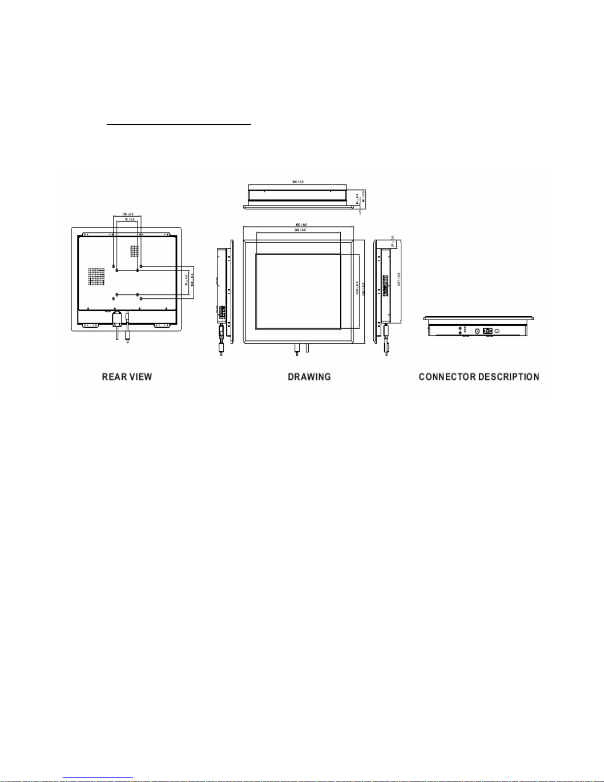
1.5 Mechanical Drawing
Figure 1.2 Dimensions of the R15B89T-IPC3
Page 16
Panel PC USER’S MANUAL
Intel Platform, High Performance PPC
15
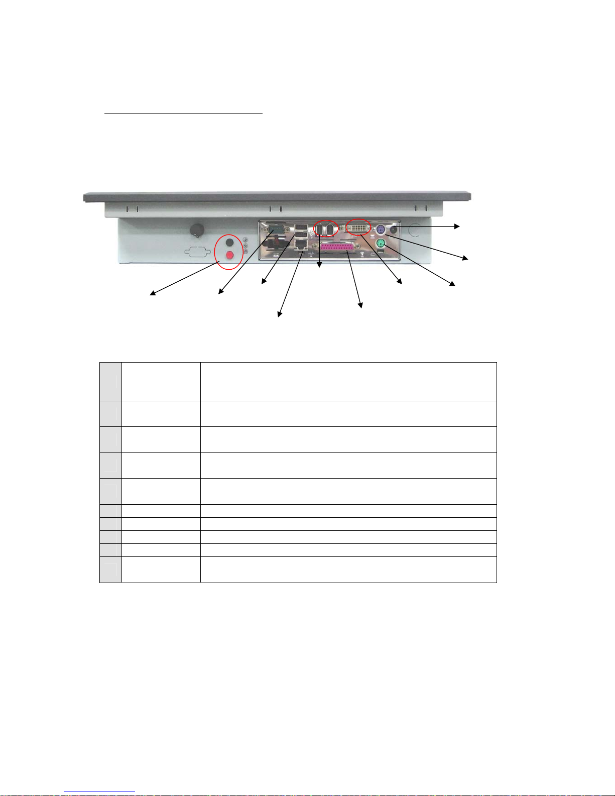
1.6 Input / Output Devices
The following figure shows the I/O arrangement of the Panel PC. The backside of
the chassis contains most of the connectors.
1
Power On/Off
&Reset
Put on/off and reset the power on your computer. The
Power hot key is located in the right of upward view in the
Panel PC.
2 COM port
9-pin male Serial Port connector that can attach a serial
mouse or other serial devices directly to the port.
3 USB port
USB-compatible devices can be plugged directly into the
USB 2.0 port.
4 RJ-45 port
Connect a network cable to the standard RJ-45 port and
get connection to the Local Area Network (LAN).
5 IEEE1394
6-pin IEEE1394 connector that can attach some digital
electronic instruments as DV, DSC to the port.
6 LPT port 25-pin female parallel port that connect to printer.
7 DVI port A DVI port that connect PPC to other LCD monitor.
8 PS/2 port Connect Keyboard to the PS/2 port.
9 PS/2 port Connect Mouse to the PS/2 port.
10 DC-in jack
Connect the power cord to the AC outlet, and connect the
power to the monitor through the AC/DC adapter.
1
Power On/Off
&Reset
10
DC-in
9
PS/2 Mouse
8
PS/2 Keyboard
4
RJ-45 port
6
LPT port
7
DVI output
5
IEEE1394
2
COM port
3
USB port
Page 17

Panel PC USER’S MANUAL
Intel Platform, High Performance PPC
16
Hardware Installation
This chapter gives hardware installation details to the Panel PC.
Sections include:
z HDD Installation
z DVD ROM Installation
C A P T E R
2
Page 18
Panel PC USER’S MANUAL
Intel Platform, High Performance PPC
17
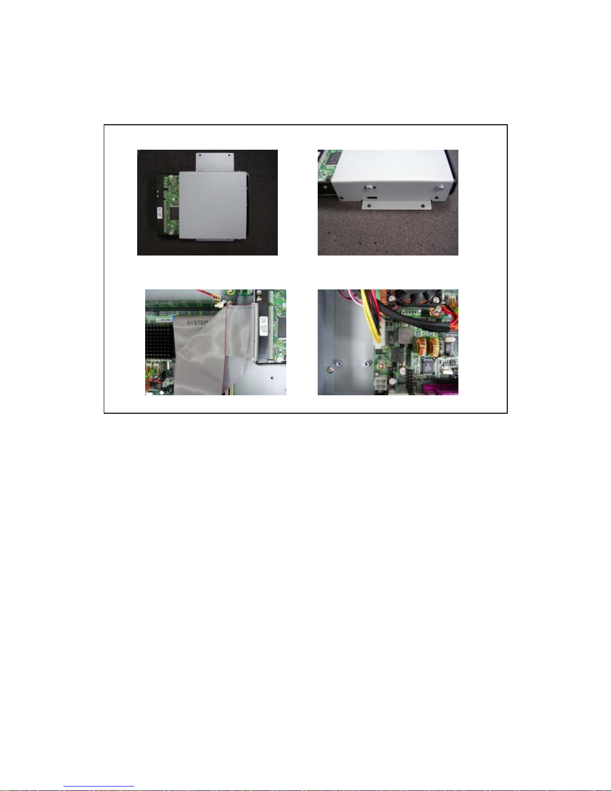
Chapter 2 Hardware Installation
The PPC is a PC-based industrial computer that is housed in aluminum alloy front
panel and heavy-duty steel chassis. And the following section will show the HDD
and DVD-ROM installation process.
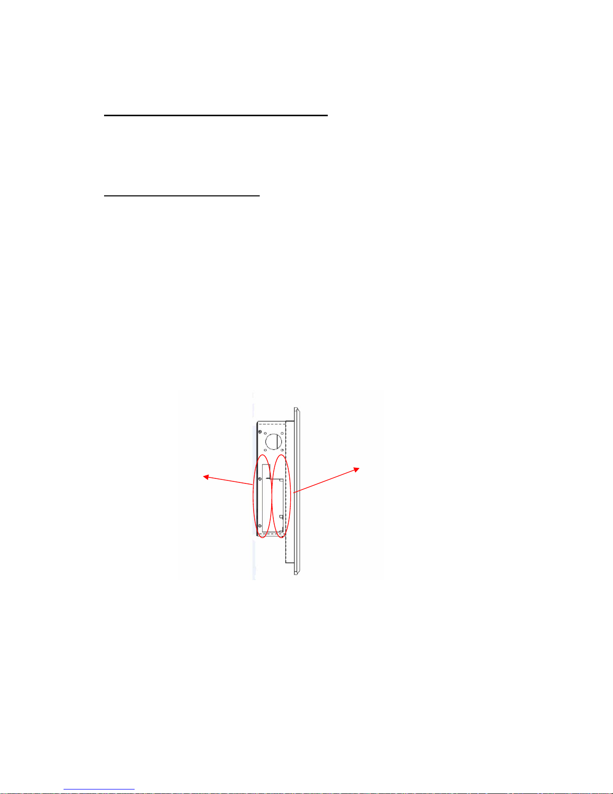
2.1 DVD ROM Installation
The PPC has a Standard Slim DVD ROM/Combo/Dual for choice (15” to 19”).
When installing the DVD ROM, please follow the steps below:
Step 1. Take out the screws and remove the PPC back cover.
Step 2. Fasten the DVD ROM to the drives shelf by 4 screws.
Step 3. Fasten screws on the side cover of the PPC.
DVD ROM
3.5” 1.44MB
+ Card Reader
Figure 2.1 DVD ROM position of the R15B89T-IPC3
Page 19
Panel PC USER’S MANUAL
Intel Platform, High Performance PPC
18
2.2 HDD Installation
The PPC has a IDE connector for 3.5” HDD, the user can install 3.5”HDD easily by
removing the side cover of HDD drive bay.
If the user intends to install DVD ROM and HDD, follow the steps below:
Step 1. Take out the screws and remove the PPC back cover.
Step 2~4. Fasten DVD with shelf by 4 screws. Fix DVD ROM within the Panel PC
with 4 screws. Connect IDE cable to the DVD IDE pin connector. Match pin
1 of the DVD and the pin 1 of the cable.
Step 5~6. Fasten the HDD to the drives shelf by 4 screws.
Step 7. Fix HDD within the Panel PC above the DVD ROM. Fasten the HDD drive
shelf inside with 4 screws.
Step8. Use the IDE cable to connect the HDD to the IDE pin connector. Match pin 1
of the HDD and the pin 1 of the cable. Connect HDD power connector as
the picture showed below.
Step 9. Fasten screws on the side cover of the PPC.
1
2
3
4
Page 20
Panel PC USER’S MANUAL
Intel Platform, High Performance PPC
19
5
6
7
8
Figure 2.2 HDD Installation of the R15B89T-IP C3
Page 21

Panel PC USER’S MANUAL
Intel Platform, High Performance PPC
20
Setting Jumpers and Connectors
This chapter describes the Jumpers and Connectors setting to
the Panel PC. Be sure to read the safety precautions before your
installation.
Sections include:
z Jumpers and Connectors
z Setting Jumpers
z Connector Definition
C A P T E R
3
Page 22
Panel PC USER’S MANUAL
Intel Platform, High Performance PPC
21
Chapter 3 Settings Jumpers and Connectors
3.1 Jumpers and Connectors
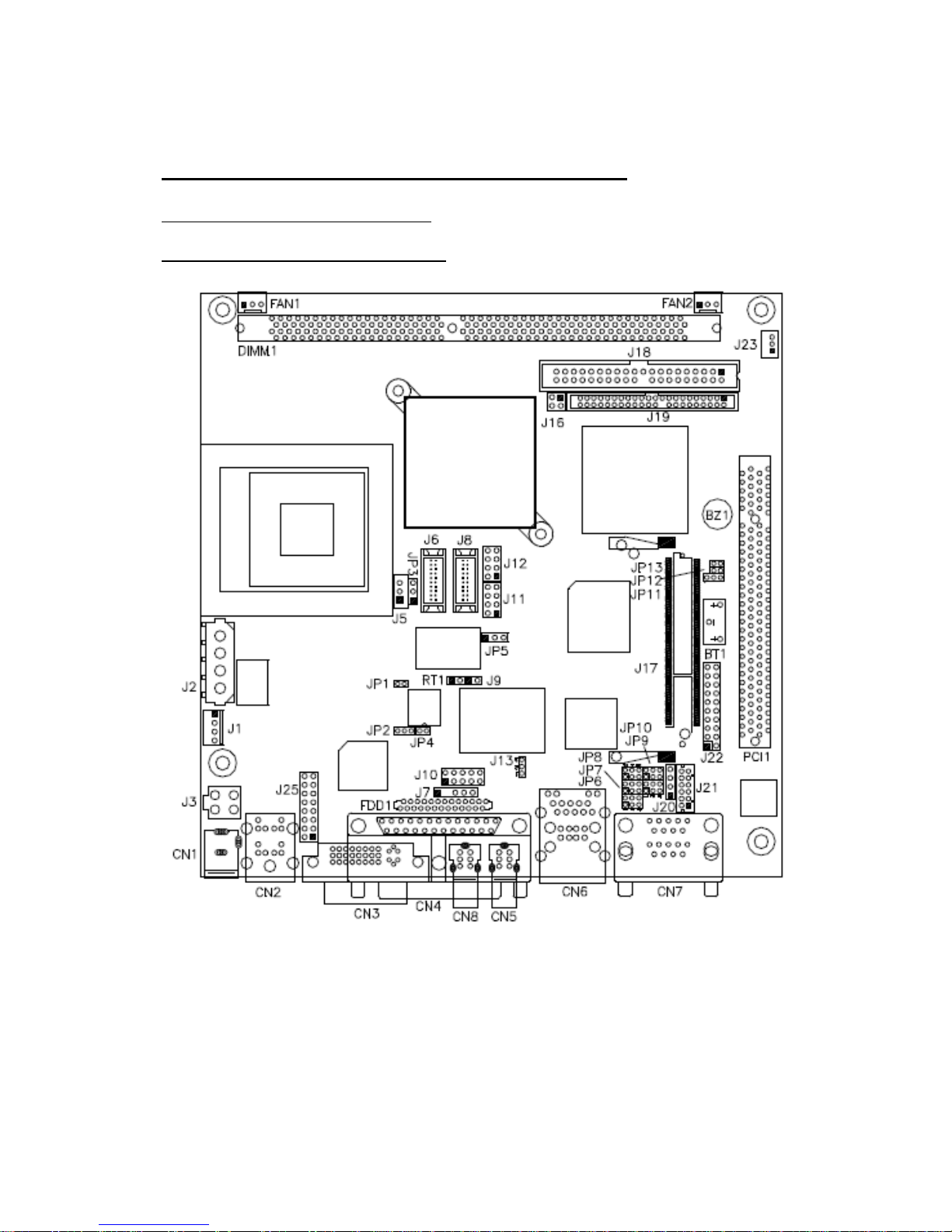
3.1.1 Jumper and Connector Layout
Figure 3.1 Jumper and Connector Layout
Page 23

Panel PC USER’S MANUAL
Intel Platform, High Performance PPC
22
3.1.2 Jumpers and Connectors
Connectors on the board are linked to external devices such as hard disk drives,
keyboard, or floppy drives. In addition, the board has a number of jumpers that
allow you to configure your system to suit your application.
The following tables list the function of each of the board's jumpers and connectors.
Table 3.1 Jumpers
Label Function
JP1 CPU Host Clock
JP2 Power Mode Setting
JP3 LVDS Power Setting
JP4 1394 Controller EEPROM Write Protect
JP6, JP7, JP8 RS232/422/485 (COM2) Selection
JP9 COM2 RS232 Pin9 Setting
JP10 COM1 RS232 Pin9 Setting
JP11 Clear CMOS Contents
JP13 Compact Flash Mode Setting
J13 Intel® 82541GI Gigabit LAN Enable/Disable
Page 24

Panel PC USER’S MANUAL
Intel Platform, High Performance PPC
23
Table 3.2 Connectors
Label Function
CN1 DC Jack for DC Adaptor
CN2 PS/2 Keyboard and PS/2 Mouse Connectors
CN3 DVI-I Connector
CN4 Parallel Port Connector
CN5, CN8 1394 Connectors
CN6 RJ45 and 2 USB Ports
CN7 COM1 and COM2 Serial Ports
J2 HDD Power Connector
J3 Internal DC-In Power Connector
J5 LCD Backlight Setting
J6, J8 Panel Connectors (1st channel, 2nd channel)
J7 IrDA Connector
J10 Digital I/O
J11, J12 USB Port Pin Header
J16 HDD Power Pin Header
J17 Mini PCI Socket
J18, J19 Primary and Secondary IDE Connectors
J20 CD-In Pin Header
J21 External Audio Connector
J22 System Function Connector
J23 Wake On LAN Connector
J24 Compact Flash Socket
J25 VGA CRT Connector
FAN1 CPU Fan Power Connector
FAN2 System Fan Power Connector
Page 25

Panel PC USER’S MANUAL
Intel Platform, High Performance PPC
24
3.2 Setting Jumpers
3.2.1 CPU Host Clock(JP1)
SEL-0 SEL_1 (JP1) SEL_2 Host Clock
1
0 100MHz (default)
1
0 133MHz
3.2.2 Power Mode Setting(JP2)
JP2 Power Mode
Simulate A TX Power
Mode (default)
AT Power Mode
3.2.3 LVDS Power Setting(JP3)
JP3 LVDS Power
+3.3V (default)
+5V
3.2.4 1394 Controller EEPROM Write Protect(JP4)
JP4 Function
Write Disable
Write Enabled
Page 26

Panel PC USER’S MANUAL
Intel Platform, High Performance PPC
25
3.2.5 RS232/422/485 (COM2) Selection(JP6, JP7, JP8)
COM1 is fixed for RS-232 use only.
COM2 is selectable for RS232, RS-422 and RS-485.
The following table describes the jumper settings for COM2 selection.
COM2
Function
RS-232 RS-422 RS-485
Jumper
Setting
(pin closed)
JP6:
3-5 & 4-6
JP7:
3-5 & 4-6
JP8:
1-2
JP6:
1-3 & 2-4
JP7:
1-3 & 2-4
JP8:
3-4
JP6:
1-3 & 2-4
JP7:
1-3 & 2-4
JP8:
5-6
3.2.6 COM2 RS232 Pin9 Setting(JP9)
Pin
Signal JP9 Signal Pin
1 RI +12V 2
3 RI (Default) RI (Default) 4
5 RI
+5V 6
COM2 Settings: Pin 1-2 short = +12V, Pin 5-6 short = +5V, Pin 3-4 RI Signal (default)
3.2.7 COM1 RS232 Pin9 Setting(JP10)
Pin
Signal JP10 Signal Pin
1 RI +12V 2
3 RI (Default) RI (Default) 4
5 RI
+5V 6
COM1 Settings: Pin 1-2 short = +12V, Pin 5-6 short = +5V, Pin 3-4 RI Signal
Page 27

Panel PC USER’S MANUAL
Intel Platform, High Performance PPC
26
3.2.8 Clear CMOS Contents(JP11)
Use JP11 to clear the CMOS contents. Note that the ATX-power connector should
be disconnected from the board before clearing CMOS.
JP11 Setting Function
Pin 1-2
Short/Closed
Normal
Pin 2-3
Short/Closed
Clear CMOS
3.2.9 Compact Flash Mode Setting(JP13)
JP13 CF Mode
Slave
Master
3.2.10 Intel® 82541GI Gigabit LAN Enable/Disable(J13)
J13 Gigabit LAN
Enable
Disable
Page 28

Panel PC USER’S MANUAL
Intel Platform, High Performance PPC
27
3.3 Connector Definitions
3.3.1 DC Jack for DC Adaptor (CN1)
The DC jack accepts input of 12V or 19V.
3.3.2 PS/2 Keyboard and PS/2 Mouse Connectors (CN2)
Signal Keyboard Mouse Signal
Keyboard data 1 1 Mouse data
N.C. 2 2 N.C.
GND 3 3 GND
5V 4 4 5V
Keyboard clock 5 5 Mouse clock
N.C. 6 6 N.C.
3.3.3 DVI-I Connector (CN3)
Signal PIN Signal
DATA 2- 1 16 HOT POWER
DATA 2+ 2 17 DATA 0Shield 2/4 3 18 DATA 0+
DATA 4- 4 19 SHIELD 0/5
DATA 4+ 5 20 DATA 5DDC CLOCK 6 21 DATA 5+
DDC DATA 7 22 SHIELD CLK
VSYNC 8 23 CLOCK DATA 1- 9 24 CLOCK +
DATA 1+ 10 C1 A RED
SHIELD 1/3 11 C2 A GREEN
DATA 3- 12 C3 A BLUE
DATA 3+ 13 C4 HYNC
DDC POWER 14 C5 A GROUND2
A GROUND 1 15 C6 A GROUND3
Page 29

Panel PC USER’S MANUAL
Intel Platform, High Performance PPC
28
3.3.4 Parallel Port Connector (CN4)
Signal PIN Signal
Line printer strobe 1 14 AutoFeed
PD0, parallel data 0 2 15 Error
PD1, parallel data 1 3 16 Initialize
PD2, parallel data 2 4 17 Select
PD3, parallel data 3 5 18 Ground
PD4, parallel data 4 6 19 Ground
PD5, parallel data 5 7 20 Ground
PD6, parallel data 6 8 21 Ground
PD7, parallel data 7 9 22 Ground
ACK, acknowledge 10 23 Ground
Busy 11 24 Ground
Paper empty 12 25 Ground
Select 13 N/A Ground
3.3.5 RJ45 and 2 USB Ports (CN6)
CN6 is a stacked connector with RJ45 on top and 2 USB ports at the bottom.
3.3.6 COM1 and COM2 Serial Ports (CN7)
CN7 is a stacked connector with COM1 on top and COM2 at the bottom .
Signal PIN Signal
DCD, Data carrier detect 1 6 RXD, Receive data
TXD, Transmit data 2 7 DTR, Data terminal ready
GND, ground 3 8 DSR, Data set ready
RTS, Request to send 4 9 CTS, Clear to send
RI, Ring indicator 5 10 Not Used
COM2 is jumper selectable for RS-232, RS-422 and RS-485.
PIN Signal
RS-232 RS-422 RS-485
1 DCD TX- DATA2 RX TX+ DATA+
3 TX RX+ NC
4 DTR RX- NC
5 Ground Ground Ground
6 DSR RTS- NC
7 RTS RTS+ NC
8 CTS CTS+ NC
9 RI CTS- NC
10 NC NC NC
Page 30

Panel PC USER’S MANUAL
Intel Platform, High Performance PPC
29
3.3.7 HDD Power Connector (J2)
Pin Signal
1 +12V
2 Ground
3 Ground
4 5V
3.3.8 Internal DC-In Power Connector (J3)
Pin Signal
1 Ground
2 Ground
3 +12V or 19V
4 +12V or 19V
3.3.9 LCD Backlight Setting (J5)
Pin Signal
1 +12V
2 Backlight Enable
3 Ground
3.3.10 Panel Connectors (1st channel, 2nd channel) (J6, J8)
The Panel connectors on board consist of the first channel (J6) and second channel
(J8) and supports 24-bit or 48-bit.
Signal PIN Signal
TX0- 2 1 TX0+
Ground 4 3 Ground
TX1- 6 5 TX1+
5V/3.3V 8 7 Ground
TX3- 10 9 TX3+
TX2- 12 11 TX2+
Ground 14 13 Ground
TXC- 16 15 TXC+
5V/3.3V 18 17 ENABKL
+12V 20 19 +12V
Page 31

Panel PC USER’S MANUAL
Intel Platform, High Performance PPC
30
3.3.11 IrDA Connector (J7)
J7 is used for an optional IrDA connector for wireless communication.
Pin Signal
1 +5V
2 No connect
3 Ir RX
4 Ground
5 Ir TX
3.3.12 Digital I/O (J10)
Signal PIN Signal
GND 1 2 VCC
OUT3 3 4 OUT1
OUT2 5 6 OUT0
IN3 7 8 IN1
IN2 9 10 IN0
3.3.13 USB Port Pin Header (J11, J12)
Signal PIN Signal
Vcc 1 5 Ground
D- 2 6 D+
D+ 3 7 D
Ground 4 8 Vcc
3.3.14 HDD Power Pin Header (J16)
Signal PIN Signal
Vcc 2 1 Vcc
NC 4 3 Ground
3.3.15 Mini PCI Socket (J17)
Page 32

Panel PC USER’S MANUAL
Intel Platform, High Performance PPC
31
3.3.16 Primary and Secondary IDE Connectors (J18, J19)
Signal PIN Signal
Reset IDE 1 2 Ground
Host data 7 3 4 Host data 8
Host data 6 5 6 Host data 9
Host data 5 7 8 Host data 10
Host data 4 9 10 Host data 11
Host data 3 11 12 Host data 12
Host data 2 13 14 Host data 13
Host data 1 15 16 Host data 14
Host data 0 17 18 Host data 15
Ground 19 20 Protect pin
DRQ0 21 22 Ground
Host IOW 23 24 Ground
Host IOR 25 26 Ground
IOCHRDY 27 28 Host ALE
DACK0 29 30 Ground
IRQ14 31 32 No connect
Address 1 33 34 No connect
Address 0 35 36 Address 2
Chip select 0 37 38 Chip select 1
Activity 39 40 Ground
3.3.17 Secondary IDE Connector (J19)
Signal PIN Signal
Reset IDE 1 2 Ground
Host data 7 3 4 Host data 8
Host data 6 5 6 Host data 9
Host data 5 7 8 Host data 10
Host data 4 9 10 Host data 11
Host data 3 11 12 Host data 12
Host data 2 13 14 Host data 13
Host data 1 15 16 Host data 14
Host data 0 17 18 Host data 15
Ground 19 20 Key
DRQ0 21 22 Ground
Host IOW 23 24 Ground
Host IOR 25 26 Ground
IOCHRDY 27 28 Host ALE
DACK0 29 30 Ground
IRQ14 31 32 No connect
Address 1 33 34 No connect
Address 0 35 36 Address 2
Chip select 0 37 38 Chip select 1
Activity 39 40 Ground
Vcc 41 42 Vcc
Ground 43 44 N.C.
Page 33

Panel PC USER’S MANUAL
Intel Platform, High Performance PPC
32
3.3.18 CD-In Pin Header (J20)
Pin Signal
1 CD Audio R
2 Ground
3 Ground
4 CD Audio L
3.3.19 External Audio Connector (J21)
J21 is a 12-pin header that is used to connect to the optional audio cable card that integrates
jacks for Line In, Line Out and Mic.
Signal PIN Signal
LINEOUT_R 1 2 LINEOUT_L
Ground 3 4 Ground
LINEIN_R 5 6 LINEIN L
Ground 7 8 Ground
Mic-In 9 10 VREFOUT
Ground 11 12 Protect pin
3.3.20 System Function Connector (J22)
J22 provides connectors for system indicators that provide light indica tion of the computer
activities and switches to change the computer status. J22 is a 20-pin header that provides
interfaces for the following functions.
Speaker: P i n s 1 – 4
This connector provides an interface to a speaker for audio tone generation. An 8-ohm
speaker is recommended.
Pin Signal
1 Speaker out
2 No connect
3 Ground
4 +5V
Page 34

Panel PC USER’S MANUAL
Intel Platform, High Performance PPC
33
Power LED: Pins 11 – 15
The power LED indicates the status of the main power switch.
Pin Signal
1 Power LED
2 No connect
3 Ground
4 No connect
5 Ground
SMI/Hardware Switch: Pins 6 and 16
This connector supports the "Green Switch" on the control panel, which, when pressed, will
force the system into the power -sa ving mode immediately.
Pin Signal
1 SMI
2 Ground
ATX Power ON Switch: Pins 7 and 17
This 2-pin connector is an “ATX Power Supply On/Off Switch” on the system that connects
to the power switch on the case. Wh en p ressed, the power switch will force the system to
power on. When pressed again, it will force the system to power off.
Reset Switch: Pins 9 and 19
The reset switch allows the user to reset the system without turning the main power switch
off and then on again. Orientation is not required when making a connection to this header.
Hard Disk Drive LED Connector: Pins 10 and 20
This connector connects to the hard drive activity LED on control panel. This LED will
flash when the HDD is being accessed.
Pin Signal
1 HDD Active
2 5V
3.3.21 Wake On LAN Connector (J23)
J23 is a 3-pin header for the Wake On LAN function. Wake On LAN will function properly
only with an ATX power supply with 5VSB that has 200mA.
Pin Signal
1 +5VSB
2 Ground
3 -PME
Page 35

Panel PC USER’S MANUAL
Intel Platform, High Performance PPC
34
3.3.22 Compact Flash Socket (J24)
3.3.23 VGA CRT Connector (J25)
Signal PIN Signal
R 1 9 +5V
G 2 10 GND
B 3 11 NC
NC 4 12 DDCDAT
GND 5 13 HSYNC
GND 6 14 VSYNC
GND 7 15 DDCCLK
GND 8 16 TV out
3.3.24 CPU Fan Power Connector (FAN1)
FAN1 is a 3-pin header for the CPU fan. The fan must be a 12V fan.
Pin Signal
1 Ground
2 +12V
3 Rotation detection
3.3.25 System Fan Power Connector (FAN2)
FAN2 is a 3-pin header for system fans. The fan must be a 12V (5 0 0mA) fan.
Pin Signal
1 Ground
2 +12V
3 Rotation detection
Page 36

Panel PC USER’S MANUAL
Intel Platform, High Performance PPC
35
AWARD BIOS Setup
This chapter describes how to set BIOS configuration data.
Sections include:
z Setting Setup
z Using Setup
z Getting Help
z In Case of Problems
z Main Manu
C A P T E R
4
Page 37

Panel PC USER’S MANUAL
Intel Platform, High Performance PPC
36
Chapter 4 AWARD BIOS Setup
4.1 Starting Setup
The Award BIOS™ is immediately activated when you first power on the computer.
The BIOS reads the system information contained in the CMOS and begins the
process of checking out the system and configuring it. When it finishes, the BIOS
will seek an operating system on one of the disks and then launch and turn control
over to the operating system.
While the BIOS is in control, the Setup program can be activated in one of two
ways:
By pressing <Del> immediately after switching the system on, or
By pressing the <Del> key when the following message appears briefly at the bottom of the
screen during the POST (Power On Self Test).
Press DEL to enter SETUP
If the message disappears before you respond and you still wish to enter Setup, restart the
system to try again by turning it OFF then ON or pressing the "RESET" button on the
system case. You may also restart by simultaneously pressing <Ctrl>, <Alt>, and <Delet e>
keys. If you do not press the keys at the correct time and the system does not boot, an error
message will be displayed and you w ill again be asked to.
Press F1 to Continue, DEL to enter SETUP
Page 38

Panel PC USER’S MANUAL
Intel Platform, High Performance PPC
37
4.2 Using Setup
In general, you use the arrow keys to highlight items, press <Enter> to select, use
the PageUp and PageDown keys to change entries, press <F1> for help and press
<Esc> to quit. The following table provides more detail about how to navigate in the
Setup program using the keyboard.
Table 4.1 Legend Keys
Up arrow Move to previous item
Down arrow Move to next item
Left arrow Move to the item in the left hand
Right arrow Move to the item in the right hand
Esc key Main Menu -- Quit and not save changes into CMOS
Status Page Setup Menu and Option Page Setup Menu -- Exit
current page and return to Main Menu
PgUp key Increase the numeric value or make changes
PgDn key Decrease the numeric value or make changes
+ key Increase the numeric value or make changes
- key Decrease the numeric value or make changes
F1 key General help, only for Status Page Setup Menu and Option
Page Setup Menu
(Shift) F2 key Change color from total 16 colors. F2 to select color forward,
(Shift) F2 to select color backward
F3 key Calendar, only for Status Page Setup Menu
F4 key Reserved
F5 key Restore the previous CMOS value from CMOS, only for
Option
Page Setup Menu
F6 key Load the default CMOS value from BIOS default table, only for
Option Page Setup Menu
F7 key Load the default
F8 key Reserved
F9 key Reserved
F10 key Save all the CMOS changes, only for Main Menu
4.2.1 Navigating Through The Menu Bar
Use the left and right arrow keys to choose the menu you want to be in.
4.2.2 To Display a Sub Menu
Use the arrow keys to move the cursor to the su b m enu you want. Then press <Enter>. A
“
” pointer marks all sub menus.
Page 39

Panel PC USER’S MANUAL
Intel Platform, High Performance PPC
38
4.3 Getting Help
Press F1 to pop up a small help window that describes the appropriate keys to use
and the possible selections for the highlighted item. To exit the Help Window press
<Esc> or the F1 key again.
4.4 In Case of Problems
If, after making and saving system changes with Setup, you discover that your
computer no longer is able to boot, the AwardBIOS™ supports an override to the
CMOS settings which resets your system to its defaults.
The best advice is to only alter settings which you thoroughly understand. To this
end, we strongly recommend that you avoid making any changes to the chipset
defaults. These defaults have been carefully chosen by both Award and your
systems manufacturer to provide the absolute maximum performance and reliability .
Even a seemingly small change to the chipset setup has the potential for causing
you to use the override.
4.5 Main Menu
Once you enter the AwardBIOS™ CMOS Setup Utility, the Main Menu will appear
on the screen. The Main Menu allows you to select from several setup functions
and two exit choices. Use the arrow keys to select among the items and press
<Enter> to accept and enter the sub-menu.
Note that a brief description of each highlighted selection appears at the bottom of
the screen.
Page 40

Panel PC USER’S MANUAL
Intel Platform, High Performance PPC
39
4.5.1 Standard CMOS Features
The items in Standard CMOS Features Menu are divided into 10 categories. Each
category includes no, one or more than one setup items. Use the arrow keys to
highlight the item and then use the <PgUp> or <PgDn> keys to select the value you
want in each item.
Page 41

Panel PC USER’S MANUAL
Intel Platform, High Performance PPC
40
4.5.1.1 Main Manu Selection
This table shows the selections that you can make on the Main Menu.
Table 4.2 Main Menu Selection
Item Options Description
Date Month DD YYYY Set the system date. Note
that the ‘Day’
automatically changes
when you set the date
Time HH : MM : SS Set the system time
IDE Primary Master Options are in its sub menu
(described in Table 3)
Press <Enter> to enter
the sub menu of detailed
options
IDE Primary Slave Options are in its sub menu
(described in Table 3)
Press <Enter> to enter
the sub menu of detailed
options
IDE Secondary Master Options are in its sub menu
(described in Table 3)
Press <Enter> to enter
the sub menu of detailed
options
IDE Secondary Master Options are in its sub menu
(described in Table 3)
Press <Enter> to enter
the sub menu of detailed
options
Drive A
Drive B
None
360K, 5.25 in
1.2M, 5.25 in
720K, 3.5 in
1.44M, 3.5 in
2.88M, 3.5 in
Select the type of floppy
disk drive installed in your
system
Video EGA/VGA
CGA 40
CGA 80
MONO
Select the default video
device
Halt On All Errors
No Errors
All, but Keyboard
All, but Diskette
All, but Disk/Key
Select the situation in
which you want the BIOS
to stop the POST
process and notify you
Base Memory N/A Displays the amount of
conventional memory
detected during boot up
Extended Memory N/A Displays the amount of
extended memory
detected during boot up
Total Memory N/A Displays the total memory
available in the system
Page 42

Panel PC USER’S MANUAL
Intel Platform, High Performance PPC
41
4.5.1.2 IDE Adapters
The IDE adapters control the hard disk drive. Use a separate sub menu to configure
each hard disk drive.
Use the legend keys to navigate through this menu and exit to the main menu. Use
Table 5.3 to configure the hard disk.
Table 4.3 Hard Disk Selection
Item Options Description
IDE HDD
Auto-detection
Press Enter Press Enter to auto-detect the HDD
on this channel. If detection is successful,
it fills the remaining fields on this menu.
IDE Primary
Master
None
Auto
Manual
Selecting ‘manual’ lets you set the
remaining fields on this screen.
Selects the type of fixed disk. "User
Type" will let you select the number
of cylinders, heads, etc. Note:
PRECOMP=65535 means NONE !
Capacity Auto Display your
disk drive
size
Disk drive capacity (Approximated).
Note that this size is usually slightly
greater than the size of a formatted
disk given by a disk checking program.
Access Mode Normal
LBA
Large
Auto
Choose the access mode for this
hard disk
The following options are selectable only if the ‘IDE Primary Master’ item is set to
‘Manual’
Cylinder Min = 0
Max = 65535
Set the number of cylinders for this
hard disk.
Head Min = 0
Max = 255
Set the number of read/write heads
Precomp Min = 0
Max = 65535
**** Warning: Setting a value of
65535 means no hard disk
Landing zone Min = 0
Max = 65535
****
Sector Min = 0
Max = 255
Number of sectors per track
Page 43

Panel PC USER’S MANUAL
Intel Platform, High Performance PPC
42
4.5.2 Advanced BIOS Features
This section allows you to configure your system for basic operation. You have the
opportunity to select the system’s default speed, boot-up sequence, keyboard
operation, shadowing and security.
4.5.2.1 CPU Feature
Press Enter to configure the settings relevant to CPU Feature.
4.5.2.2 Virus Warning
If this option is enabled, an alarm message will be displayed when trying to write
on the boot sector or on the partition table on the disk, which is typical of the virus.
4.5.2.3 CPU L1 and L2 Cache / CPU L3 Cache
Cache memory is additional memory that is much faster than conventional DRAM
(system memory). CPUs from 486-type on up contain internal cache memory, and
most, but not all, modern PCs have additional (external) cache memory. When the
CPU requests data, the system transfers the requested data from the main DRAM
into cache memory, for even faster access by the CPU. These items allow you to
enable (speed up memory access) or disable the cache function. By default, these
items are Enabled.
Page 44

Panel PC USER’S MANUAL
Intel Platform, High Performance PPC
43
4.5.2.4 Quick Power On Self Test
When enabled, this field speeds up the Power On Self Test (POST) after the system
is turned on. If it is set to Enabled, BIOS will skip some items.
4.5.2.5 First/Second/Third Boot Device
These fields determine the drive that the system searches first for an operating
system. The options available include Floppy, LS120, HDD-0, SCSI, CDROM,
HDD-1, HDD-2, HDD-3, ZIP100, USB-FDD, USB-CDROM, USB-HDD and Disable.
4.5.2.6 Boot Other Device
These fields allow the system to search for an OS from other devices other than the
ones selected in the First/Second/Third Boot Device.
4.5.2.7 Swap Floppy Drive
This item allows you to determine whether or not to enable Swap Floppy Drive.
When enabled, the BIOS swaps floppy drive assignments so that Drive A becomes
Drive B, and Drive B becomes Drive A. By default, this field is set to Disabled.
4.5.2.8 Boot Up Floppy Seek
This feature controls whether the BIOS checks for a floppy drive while booting up. If
it cannot detect one (either due to improper configuration or its absence), it will flash
an error message.
4.5.2.9 Boot Up NumLock Status
This allows you to activate the NumLock function after you power up the system.
4.5.2.10 Gate A20 Option
This field allows you to select how Gate A20 is worked. Gate A20 is a device used
to address memory above 1 MB.
4.5.2.11 Typematic Rate Setting
When disabled, continually holding down a key on your keyboard will generate only
one instance. When enabled, you can set the two typematic controls listed next. By
default, this field is set to Disabled.
4.5.2.12 Typematic Rate (Chars/Sec)
When the typematic rate is enabled, the system registers repeated keystrokes
speeds. Settings are from 6 to 30 characters per second.
Page 45

Panel PC USER’S MANUAL
Intel Platform, High Performance PPC
44
4.5.2.13 Typematic Delay (Msec)
When the typematic rate is enabled, this item allows you to set the time interval for
displaying the first and second characters. By default, this item is set to 250msec.
4.5.2.14 Security Option
This field allows you to limit access to the System and Setup. The default value is
Setup. When you select System, the system prompts for the User Password every
time you boot up. When you select Setup, the system always boots up and prompts
for the Supervisor Password only when the Setup utility is called up.
4.5.2.15 APIC Mode
APIC stands for Advanced Programmable Interrupt Controller. The default setting is
Enabled.
4.5.2.16 MPS Version Control for OS
This option is specifies the MPS (Multiprocessor Specification) version for your
operating system. MPS version 1.4 added extended configuration tables to improve
support for multiple PCI bus configurations and improve future expandability. The
default setting is 1.4.
4.5.2.17 OS Select for DRAM > 64MB
This option allows the system to access greater than 64MB of DRAM memory when
used with OS/2 that depends on certain BIOS calls to access memory. The default
setting is Non-OS/2.
4.5.2.18 Report No FDD For WIN 95
If you are using Windows 95/98 without a floppy disk drive, select Enabled to
release IRQ6. This is required to pass Windows 95/98's SCT test. You should also
disable the Onboard FDC Controller in the Integrated Peripherals screen when
there's no floppy drive in the system. If you set this feature to Disabled, the BIOS
will not report the missing floppy drive to Win95/98.
4.5.2.19 Small Logo (EPA) Show
The EPA logo appears at the right side of the monitor screen when the system is
boot up. The default setting is Enabled.
Page 46

Panel PC USER’S MANUAL
Intel Platform, High Performance PPC
45
4.5.3 Advanced Chipset Features
4.5.3.1 DRAM Timing Selectable
This option refers to the method by which the DRAM timing is selected. The default
is By SPD.
4.5.3.2 CAS Latency Time
You can configure CAS latency time in HCLKs as 2 or 2.5 or 3. The system board
designer should set the values in this field, depending on the DRAM installed. Do
not change the values in this field unless you change specifications of the installed
DRAM or the installed CPU.
4.5.3.3 Active to Precharge Delay
The default setting for the Active to Precharge Delay is 7.
4.5.3.4 DRAM RAS# to CAS# Delay
This option allows you to insert a delay between the RAS (Row Address Strobe)
and CAS (Column Address Strobe) signals. This delay occurs when the SDRAM is
Page 47

Panel PC USER’S MANUAL
Intel Platform, High Performance PPC
46
written to, read from or refreshed. Reducing the delay improves the performance of
the SDRAM.
4.5.3.5 DRAM RAS# Precharge
This option sets the number of cycles required for the RAS to accumulate its charge
before the SDRAM refreshes. The default setting for the Active to Precharge Delay
is 3.
4.5.3.6 DRAM Data Integrity Mode
Select ECC if your memory module supports it. The memory controller will detect
and correct single-bit soft memory errors. The memory controller will also be able to
detect double-bit errors though it will not be able to correct them. This provides
increased data integrity and system stability.
4.5.3.7 MGM Core Frequency
This field sets the frequency of the DRAM memory installed. The default setting is
Auto Max 266MHz.
4.5.3.8 System BIOS Cacheable
The setting of Enabled allows caching of the system BIOS ROM at F000h-FFFFFh,
resulting in better system performance. However, if any program writes to this
memory area, a system error may result.
4.5.3.9 Video BIOS Cacheable
The Setting Enabled allows caching of the video BIOS ROM at C0000h-F7FFFh,
resulting in better video performance. However, if any program writes to this
memory area, a system error may result.
4.5.3.10 Memory Hole At 15M-16M
In order to improve performance, certain space in memory can be reserved for ISA
cards. This memory must be mapped into the memory space below 16 MB. The
choices are Enabled and Disabled.
4.5.3.11 Delayed Transaction
The chipset has an embedded 32-bit posted write buffer to support delay
transactions cycles. Select Enabled to support compliance with PCI specification
version 2.1.
4.5.3.12 Delay Prior to Thermal
This field activates the CPU thermal function after the systems boots for the set
number of minutes. The options are 16Min and 64Min.
Page 48

Panel PC USER’S MANUAL
Intel Platform, High Performance PPC
47
4.5.3.13 AGP Aperture Size
The field sets aperture size of the graphics. The aperture is a portion of the PCI
memory address range dedicated for graphics memory address space. Host cycles
that hit the aperture range are forwarded to the AGP without any translation. The
default setting is 64M.
4.5.3.14 On-Chip VGA
The default setting is Enabled.
4.5.3.15 On-Chip Frame Buffer Size
The default setting is 32MB. The options available include 1MB, 4MB, 8MB and
16MB.
4.5.3.16 Boot Display
The default setting is CRT+DVI. The options available include some combinations
with LVDS and TV-out. The B89 supports dual view (CRT with LVDS or TV-out).
4.5.3.17 TV Standard
The default setting is Off.
4.5.3.18 Video Connector
The default setting is Automatic.
4.5.3.19 TV Format
The default setting is Auto.
4.5.3.20 Panel Scaling
The default setting is Auto. The options available include On and Off.
4.5.3.21 Panel Number
These fields allow you to select the LCD Panel type. The default values for these
ports are:
640x480
800x480
800x600
1024x768
1280x720
1280x768
1280x1024
Page 49

Panel PC USER’S MANUAL
Intel Platform, High Performance PPC
48
1366x768
1400x1050
1600x1200
1600x1200A
4.5.3.22 Panel Protocol
These fields allow you to select the LCD Panel Protocol. The default values for
these parts are:
18bit 1ch
24bit 1ch SPGM
24bit 1ch OpenLDI
18bit 2ch
24bit 2ch SPGM
24bit 2ch OpenLDI
4.5.4 Integrated Peripherals
This section sets configurations for your hard disk and other integrated peripherals.
The first screen shows three main items for user to select. Once an item selected, a
submenu appears. Details follow.
Page 50

Panel PC USER’S MANUAL
Intel Platform, High Performance PPC
49
4.5.4.1 OnChip Primary/Secondary PCI IDE
The integrated peripheral controller contains an IDE interface with support for two
IDE channels. Select Enabled to activate each channel separately.
4.5.4.2 IDE Primary/Secondary Master/Slave PIO
These fields allow your system hard disk controller to work faster. Rather than have
the BIOS issue a series of commands that transfer to or from the disk drive, PIO
(Programmed Input/Output) allows the BIOS to communicate with the controller and
CPU directly. The system supports five modes, numbered from 0 (default) to 4,
which primarily differ in timing. When Auto is selected, the BIOS will select
the best available mode.
4.5.4.3 IDE Primary/Secondary Master/Slave UDMA
These fields allow your system to improve disk I/O throughput to 33Mb/sec with the
Ultra DMA/33 feature. The options are Auto and Disabled.
Page 51

Panel PC USER’S MANUAL
Intel Platform, High Performance PPC
50
4.5.4.4 IDE HDD Block Mode
This field allows your hard disk controller to use the fast block mode to transfer data
to and from your hard disk drive.
4.5.4.5 USB Controller
The options for this field are Enabled and Disabled. By default, this field is set to
Enabled.
4.5.4.6 USB 2.0 Controller
The options for this field are Enabled and Disabled. By default, this field is set to
Enabled. In order to use USB 2.0, necessary OS drivers must be installed first.
Please update your system to Windows 2000 SP4 or Windows XP SP2.
4.5.4.7 USB Keyboard Support
The options for this field are Enabled and Disabled. By default, this field is set to
Disabled.
4.5.4.8 USB Mouse Support
The options for this field are Enabled and Disabled. By default, this field is set to
Disabled.
4.5.4.9 AC97 Audio
The default setting of the AC97 Audio is Auto.
4.5.4.10 Init Display First
The default setting is PCI Card.
4.5.4.11 Power On After Fail
The setting configures the system power on status when power is restored to the
system after a power failure occurrence. The default setting is Off.
4.5.4.12 Onboard FDC Controller
Select Enabled if your system has a floppy disk controller (FDC) installed on the
motherboard and you wish to use it. If you install an add-in FDC or the system has
no floppy drive, select Disabled in this field. This option allows you to select the
onboard FDD port.
Page 52

Panel PC USER’S MANUAL
Intel Platform, High Performance PPC
51
4.5.4.13 Onboard Serial/Parallel Port
These fields allow you to select the onboard serial and parallel ports and their
addresses. The default values for these ports are:
Serial Port 1 3F8/IRQ4
Serial Port 2 2F8/IRQ3
Parallel Port 3 78H/IRQ7
4.5.4.14 UART Mode Select
This field determines the UART 2 mode in your computer. The default value is
Normal. Other options include IrDA and ASKIR.
4.5.4.15 Parallel Port Mode
This field allows you to determine parallel port mode function.
SPP Standard Printer Port
EPP Enhanced Parallel Port
ECP Extended Capabilities Port
4.5.5 Power Management Setup
The Power Management Setup allows you to save energy of your system
effectively.
Page 53

Panel PC USER’S MANUAL
Intel Platform, High Performance PPC
52
4.5.5.1 Power Supply Type
Use this field to select the power supply type used in the system. The default setting
is A TX.
4.5.5.2 ACPI Function
Enable this function to support ACPI (Advance Configuration and Power Interface).
4.5.5.3 Power Management
This field allows you to select the type of power saving management modes.
There are four selections for Power Management.
Min. Power Saving Minimum power management
Max. Power Saving Maximum power management.
User Define Each of the ranges is from 1 min. to 1hr. Except for HDD Power Down
which ranges from 1 min. to 15 min.
4.5.5.4 Video Off Method
This field defines the Video Off features. There are three options.
V/H SYNC + Blank Default setting, blank the screen and turn off
Page 54

Panel PC USER’S MANUAL
Intel Platform, High Performance PPC
53
vertical and horizontal scanning.
DPMS Allows BIOS to control the video display.
Blank Screen Writes blanks to the video buffer.
4.5.5.5 Video Off In Suspend
When enabled, the video is off in suspend mode. The default setting is Yes.
4.5.5.6 Suspend Type
The default setting for the Suspend Type field is Stop Grant.
4.5.5.7 Modem Use IRQ
This field sets the IRQ used by the Modem. By default, the setting is 3.
4.5.5.8 Suspend Mode
When enabled, and after the set time of system inactivity, all devices except the
CPU will be shut off.
4.5.5.9 HDD Power Down
When enabled, and after the set time of system inactivity, the hard disk drive will be
powered down while all other devices remain active.
4.5.5.10 Soft-Off by PWRBTN
This field defines the power-off mode when using an ATX power supply. The Instant
Off mode allows powering off immediately upon pressing the power button. In the
Delay 4 Sec mode, the system powers off when the power button is pressed for
more than four seconds or enters the suspend mode when pressed for less than 4
seconds.
4.5.5.11 CPU THRM-Throttling
When the system enters Doze mode, the CPU clock runs only part of the time. You
may select the percent of time that the clock runs.
4.5.5.12 Wake up by PCI Card
By default, this field is disabled.
4.5.5.13 Power On by Ring
This field enables or disables the power on of the system through the modem
connected to the serial port or LAN.
Page 55

Panel PC USER’S MANUAL
Intel Platform, High Performance PPC
54
4.5.5.14 Resume by Alarm
This field enables or disables the resumption of the system operation. When
enabled, the user is allowed to set the Date and Time.
4.5.5.15 Reload Global Timer Events
The HDD, FDD, COM, LPT Ports, and PCI PIRQ are I/O events that can prevent the
system from entering a power saving mode or can awaken the system from such a
mode. When an I/O device wants to gain the attention of the operating system, it
signals this by causing an IRQ to occur. When the operating system is ready to
respond to the request, it interrupts itself and performs the service.
4.5.6 PNP/PCI Configurations
This option configures the PCI bus system. All PCI bus systems on the system use
INT#, thus all installed PCI cards must be set to this value.
4.5.6.1 Reset Configuration Data
This field allows you to determine whether to reset the configuration data or not.
The default value is Disabled.
4.5.6.2 Resources Controlled by
This PnP BIOS can configure all of the boot and compatible devices automatically
with the use of a use a PnP operating system such as Windows 95.
4.5.6.3 PCI/VGA Palette Snoop
Some non-standard VGA display cards may not show colors properly. This field
allows you to set whether or not MPEG ISA/VESA VGA cards can work with
PCI/VGA. When this field is enabled, a PCI/VGA can work with an MPEG ISA/VESA
Page 56

Panel PC USER’S MANUAL
Intel Platform, High Performance PPC
55
VGA card. When this field is disabled, a PCI/VGA cannot work with an MPEG
ISA/VESA card.
4.5.7 PC Health Status
This section shows the parameters in determining the PC Health Status. These
parameters include temperatures, fan speeds and voltages.
4.5.7.1 CPU Warning Temperature
This field allows the user to set the temperature so that when the temperature is
reached, the system sounds a warning. This function can help prevent damage to
the system that is caused by overheating.
4.5.7.2 Temperatures/Voltages
These fields are the parameters of the hardware monitoring function feature of the
motherboard. The values are read-only values as monitored by the system and
show the PC health status.
4.5.7.3 Shutdown Temperature
This field allows the user to set the temperature by which the system automatically
shuts down once the threshold temperature is reached. This function can help
prevent damage to the system that is caused by overheating.
4.5.7.4 Smart Fan Temperature
This field enables or disables the smart fan feature. At a certain temperature, the
Page 57

Panel PC USER’S MANUAL
Intel Platform, High Performance PPC
56
fan starts turning. Once the temperature drops to a certain level, it stops turning
again.
4.5.8 Frequency/Voltage Control
This section shows the user how to configure the processor frequency.
4.5.8.1 Auto Detect PCI Clk
This field enables or disables the auto detection of the PCI clock.
4.5.8.2 Spread Spectrum Modulated
This field sets the value of the spread spectrum. The default setting is Disabled.
This field is for CE testing use only
4.5.9 Load Fail-Safe Defaults
This option allows you to load the troubleshooting default values permanently
stored in the BIOS ROM. These default settings are non-optimal and disable all
high-performance features.
4.5.10 Load Optimized Defaults
This option allows you to load the default values to your system configuration.
These default settings are optimal and enable all high performance features.
4.5.11 Set Supervisor Password
These two options set the system password. Supervisor Password sets a password
that will be used to protect the system and Setup utility. User Password sets a
password that will be used exclusively on the system. To specify a password,
highlight the type you want and press <Enter>. The Enter Password: message
prompts on the screen. Type the password, up to eight characters in length, and
press <Enter>. The system confirms your password by asking you to type it again.
After setting a password, the screen automatically returns to the main screen.
To disable a password, just press the <Enter> key when you are prompted to enter
the password. A message will confirm the password to be disabled. Once the
password is disabled, the system will boot and you can enter Setup freely.
Page 58

Panel PC USER’S MANUAL
Intel Platform, High Performance PPC
57
4.5.12 Save & Exit Setup
This option allows you to determine whether or not to accept the modifications. If
you type “Y”, you will quit the setup utility and save all changes into the CMOS
memory. If you type “N”, you will return to Setup utility.
4.5.13 Exit Without Saving
Select this option to exit the Setup utility without saving the changes you ha ve made
in this session. Typing “Y” will quit the Setup utility without saving the modifications.
Typing “N” will return you to Setup utility.
Page 59

Panel PC USER’S MANUAL
Intel Platform, High Performance PPC
58
Driver Installation
This chapter gives driver installation information to the Panel PC.
Sections include:
z Intel Chipset Software Installation Utility
z VGA Drivers Installation
z AC97 Codec Audio Driver Installation
z Intel PRO LAN Drivers Installation
C A P T E R
5
Page 60

Panel PC USER’S MANUAL
Intel Platform, High Performance PPC
59
Chapter 5 Driver Installation
5.1 Intel Chipset Software Installation Utility
The Intel Chipset Drivers should be installed first before the software drivers to
enable Plug & Play INF support for Intel chipset components. Follow the instructions
below to complete the installation under Windows 98SE/ME/2000/XP.
1. Insert the CD that comes with the board. Click Intel Chipsets and then Intel(R)
855GME Chipset Drivers.
2. Click Intel(R) Chipset Software Installation Utility.
3. When the Welcome screen appears, click Next to continue.
Page 61

Panel PC USER’S MANUAL
Intel Platform, High Performance PPC
60
4. Click Yes to accept the software license agreement and proceed with the
installation process.
5. On Readme Information screen, click Next to continue the installation.
6. The Setup process is now complete. Click Finish to restart the computer and for
changes to take effect. When the computer has restarted, the system will be able to
find some devices. Restart your computer when prompted.
Page 62

Panel PC USER’S MANUAL
Intel Platform, High Performance PPC
61
5.2 VGA Drivers Installation
To install the VGA drivers, follow the steps below to proceed with the installation.
1. Insert the CD that comes with the motherboard. Click Intel Chipsets and then
Intel(R) 855GME Chipset Drivers.
2. Click Intel(R) 855GME Chipset Family Graphics Driver.
3. When the Welcome screen appears, click Next to continue.
4. Click Yes to to agree with the license agreement and continue the installation.
5. Restart the computer as promted and for changes to take effect.
<Attention>
Please update the latest VGA Driver in the User’s Manual CD “VGA Driver”
program.
Page 63

Panel PC USER’S MANUAL
Intel Platform, High Performance PPC
62
5.3 AC97 Codec Audio Driver Installation
Follow the steps below to install the Realtek AC97 Codec Audio Drivers.
1. Insert the CD that comes with the motherboard. Click Intel Chipsets and then
Intel(R) 855GME Chipset Drivers.
2. Click Realtek AC'97 Codec Audio Driver.
3. Click Finish to restart the computer and for changes to take effect. .
Page 64

Panel PC USER’S MANUAL
Intel Platform, High Performance PPC
63
5.4 Intel PRO LAN Drivers Installation
Follow the steps below to complete the installation of the Intel PRO LAN drivers.
1. Insert the CD that comes with the motherboard. Click LAN Card and then Intel(R)
PRO LAN Drivers.
2. Click Install Base Software to continue.
3. When prompted, please to restart the computer for new settings to take effect.
Page 65

Panel PC USER’S MANUAL
Intel Platform, High Performance PPC
64
Touch Screen
This chapter gives some information about touch screen solution
installed on the Panel PC.
Sections include:
z Introduction
z The AccuTouch Controllers
z Driver Software
C A P T E R
6
Page 66

Panel PC USER’S MANUAL
Intel Platform, High Performance PPC
65
Chapter 6 Touchscreen
6.1 Introduction
The PPC supports two Touch Panel Solution- Elo AccuTouch touchscreen and
Premier Touch system. Both the two touchscreen system consists of a touchscreen
and an electronic touchscreen controller.
The Elo AccuTouch and Premier touchscreen is based on patented resistive
technology. The touchscreen may be a flat, spherical, or cylindrical and is installed
over the face of the display. Since its shape matches that of the display face, the
touchscreen has excellent clarity and minimal parallax.
6.2 The Elo AccuTouch Driver Installation
Elo AccuTouch driver software provides a consistent software interface among all
Elo touchscreens and controllers.Go to www.elotouch.com/Support/dnld.asp
for a
complete list of available drivers.
For Driver Installation, please install the “Elo TouchSystem TouchTools CD” for
Windows XP, Wi ndows 2000, Windows Me, Windows 98, Wi ndows 95, Windows NT,
Windows CE 2.x, 3.0, 4.x, Windows XP Embedded, Windows 3.1, DOS, OS/2 Warp,
and Apple Macintosh. Just follow the step by step to install the driver.
Page 67

Panel PC USER’S MANUAL
Intel Platform, High Performance PPC
66
6.2.1 Configuration Utility
After finishing the installation, please follow the steps to test the configuration utility.
(1) Enter “My Computer”, click the “Elo touchscreen” shortcut function.
(2) Click “Align” function key to go to next step.
Page 68

Panel PC USER’S MANUAL
Intel Platform, High Performance PPC
67
(3) Correct 4 point locations on screen with the Panel. Screen display as follows.
(4) Touch the “yes” function if the cursor follows your finger and finish the utility test.
Page 69

Panel PC USER’S MANUAL
Intel Platform, High Performance PPC
68
6.3 The Premier Touch Driver Installation
TouchKit is the Premier Touch software, which contains drivers of the touch panel
controllers for the specified communication connectors, RS232, PS/2 and USB, and
the other two utilities.
The two utilities are as follows:
(1) Touch Tray support
This is utility for emulating the right and left button of mouse through controlling
touch panel. Users can toggle between right or left mouse buttons by this utility.
(2) Configuration support
The calibration and draw test of touch panel are done by this utility. Besides, users
can add or remove for new RS-232 or PS/2 touch panel devices.
Follow these steps to install TouchKit.
(1) Put the TouchKit CD to CD-ROM.
(2) Open the Win2000_XP directory.
(3) Double click the Setup.exe, then windows starts to run the installation program.
Notice that do not plug the USB controller on the system before the installation
has been finished.
(4) Just click [Next >] button to continue installation.
(5) Following the step by step to finish the driver installation.
Page 70

Panel PC USER’S MANUAL
Intel Platform, High Performance PPC
69
6.3.1 Configuration Utility
After finishing the installation, please follow the steps to test the configuration utility.
(1) Click the “TouchKit” shortcut function in the desktop.
(2) Enter “General” function and choose the language you need. Then go to next
step.
Page 71

Panel PC USER’S MANUAL
Intel Platform, High Performance PPC
70
(3) Correct 4 point locations on screen with the Panel. Screen display as follows
(4) Play “yes” to continue if 4 points calibration test is fine and finish the test.
 Loading...