

Page 1

Intel® Celeron® Processor 1.66 GHz/
1.83 GHz
Datasheet
January 2007
Order Number: 315 876-002
Page 2

Intel® Celeron® Processor 1.66 GHz/1.83 GHz—
Lega l Li nes and Discl a imers
INFORMATION IN THIS DOCUMENT IS PROVIDED IN CONNECTION WITH INTEL® PRODUCTS. NO LICENSE, EXPRESS OR IMPLIED, BY ESTOPPEL OR
OTHERWISE, TO ANY INTELLECTUAL PROPERTY RIGHTS IS GRANTED BY THIS DOCUMENT. EXCEPT AS PROVIDED IN INTEL'S TERMS AND CONDITIONS
OF SALE FOR SUCH PRODUCTS, INTEL ASSUMES NO LIABILITY WHAT SOEVER, AND INTEL DISCLAIMS ANY EXPRESS OR IMPLIED WARRANTY, RELA TING
TO SALE AND/OR USE OF INTEL PRODUCTS INCLUDING LIABILITY OR WARRANTIES RELATING TO FITNESS FOR A PARTICULAR PURPOSE,
MERCHANTABILITY, OR INFRINGEMENT OF ANY PATENT, COPYRIGHT OR OTHER INTELLECTUAL PROPERTY RIGHT. Intel products are not intended for
use in medical, life saving, life sustaining, critical control or safety systems, or in nuclear facility applications.
Intel may make changes to specifications and product descriptions at any time, without notice.
Intel Corporation may have patents or pending patent applications, trademarks, copyrights, or other intellectual property rig h ts that relate to the
present e d subject matter. The furn i shi ng o f do c um ent s and other mate rial s a nd i nfo rm at io n do es n ot provide any license, express or imp lied, by esto ppe l
or otherwise, to any such patents, trademarks, copyrights, or other intellectual property rights.
Designers must not rely on the absence or characteristics of any features or instructions marked “reserved” or “undefined.” Intel reserves these for
future definition and shall have no responsibility w hatsoever for conflicts or incompatibilities arising from future changes to them.
Intel processor numbers are not a measure of performance. Processor numbers differentiate featur es within each processor family, not across different
processor families. See http://www.intel.com/products/processor_number for details.
The Intel® Celero n® Processor 1.66 GHz/1.83 GHz may contain design defects or errors known as errata which may cause the product to deviate fr om
published specifications. Current characterized errata are available on request.
Hyper-Threading Technology requires a computer system with an Intel® Pentium® 4 processor supporting HT Technology and a HT Technology enabled
chipset, BIOS and operating system. Performance will vary depending on the specific hardware and software you use. See http://www.intel.com/
products/ht/Hyperthreading_more.htm for additional information.
Contact your local Intel sales office or your distributor to obtain the latest specifications and before placing your product order.
Copies of documents w hich have an order number and are referenced in this document, or other Intel literature may be obtained by calling
1-800-548-4725 or by visiting Intel's website at http://www.intel.com.
BunnyPeople, Celeron, Celeron Inside, Centrino, Centrino logo, Core Inside, Dialogic, FlashFile, i960, InstantIP, Intel, Intel logo, Intel386, Intel486,
Intel740, IntelDX2, IntelDX4, IntelSX2, Intel Core, Intel Inside, Intel Inside logo, Intel. Leap ahead., Intel. Leap ahead. logo, Intel NetBurst, Intel
NetMerge, Intel NetStructure, Intel SingleDriver, Intel SpeedStep, Intel StrataFlash, Intel Viiv, Intel vPro, Intel XScale, IPLink, Itanium, Itanium Inside,
MCS, MMX, Oplus, OverDrive, PDCharm, Pentium, Pentium Inside, skoool, Sound Mark, The Journey Inside, VTune, Xeon, and Xeon Inside are
trademarks or register ed trademarks of Intel Corporation or its subsidiaries in the United States and other countries.
*Other na m es and bra nds may be claimed as t he pro perty of others .
Copyright © 2007, Intel Corporation. All Rights Reserved.
®
Celeron® Processor 1.66 GHz/1.83 GHz
Intel
DS January 2007
2 Order Nu mber: 315876 - 00 2
Page 3

Contents—Intel
®
Celeron® Processor 1.66 GHz/1.83 GHz
Contents
1.0 Introduction..............................................................................................................6
1.1 Terminology .......................................................................................................7
1.2 References .........................................................................................................8
1.3 State of Data......................................................................................................9
2.0 Low Power Features................................................................................................10
2.1 Clock Control and Low Power States ....................................................................10
2.2 Enhanced Intel
2.3 Extended Halt State (C1E)..................................................................................13
3.0 Electrical Specifications...........................................................................................15
3.1 Front Side Bus and GTLREF ................................................................................ 15
3.2 Power and Ground Pins......................................................................................15
3.3 Decoupling Guidelines........................................................................................15
3.4 Voltage Identification and Power Sequencing ........................................................16
3.5 Catastrophic Thermal Protection.......................................................................... 18
3.6 Signal Terminations and Unused Pins...................................................................18
3.7 FSB Frequency Select Signals (BSEL[2:0])............................................................18
3.8 FSB Signal Groups.............................................................................................19
3.9 CMOS Signals ...................................................................................................20
3.10 Maximum Ratings..............................................................................................20
3.11 Processor DC Specifications ................................................................................20
4.0 Package Mechanical Specifications and Pin Information..........................................25
4.1 Package Mechanical Specifications.......................................................................25
4.2 Processor Pin-Out and Pin List.............................................................................28
5.0 Thermal Specifications and Design Considerations ..................................................61
5.1 Thermal Specifications .......................................................................................62
®
SpeedStep® Technology (EIST)...................................................13
Figures
1 Package-Level Low Power States................................................................................10
2 Core Low Power States.............................................................................................11
3 Active VCC and ICC Load Line for Intel
®
Celeron® Processor 1.66 GHz/1.83 GHz.............. 22
4 Micro-FCPGA Package Top and Bottom Views...............................................................25
5 Micro-FCPGA Processor Package Drawing (Sheet 1) ................... ...................................26
6 Micro-FCPGA Processor Package Drawing (Sheet 2) ................... ...................................27
7 The Coordinates of the Processor Pins as Viewed From the Top of the Package................. 29
Tables
1 Terminology ..............................................................................................................7
2 References................................................................................................................ 8
3Intel
4 BSEL[2:0] Encoding for BCLK Frequency.....................................................................18
5 FSB Pin Groups........................................................................................................19
6 Processor DC Absolute Maximum Ratings ....................................................................20
7 Voltage and Current Specifications for the Intel
8 AGTL+ Signal Group DC Specifications........................................................................22
9 CMOS Signal Group DC Specifications.........................................................................23
10 Open Drain Signal Group DC Specifications..................................................................24
11 Signal Description....................................................................................................30
January 2007 DS
Order Nu mber: 315876 - 00 2 3
®
Celeron® Processor 1.66 GHz/1.83 GHz VID Map................................................16
®
Celeron® Processor 1.66 GHz/1.83 GHz.. 21
Intel® Celeron® Process or 1.66 GHz/1.83 GHz
Page 4

Intel® Celeron® Processor 1.66 GHz/1.83 GHz—Contents
12 Quad-Pumped Signal Groups......................................................................................32
13 DINV[3:0]# Assignment To Data Bus..........................................................................32
14 Alphabetical Signal Listing .........................................................................................37
15 Alphabetical Pin Listing..............................................................................................49
16 Power Specifications for the Intel
®
Celeron® Processor 1.66 GHz/1.83 GHz......................61
17 Thermal Diode Interface............................................................................................63
18 Thermal “Diode” Parameters using Diode Mode.............................................................63
19 Thermal “Diode” n
and Diode Correction Toffset.......................................................64
trim
®
Celeron® Processor 1.66 GHz/1.83 GHz
Intel
DS January 2007
4 Order Nu mber: 315876 - 00 2
Page 5
Revision History—Intel
®
Celeron® Processor 1.66 GHz/1.83 GHz
Revision History
Date Revision Description
November 2006 001 Initial public release.
January 2007 002 Added information for Intel® Celeron® Process o r 1. 83 GHz
January 2007 DS
Order Nu mber: 315876 - 00 2 5
Intel® Celeron® Process or 1.66 GHz/1.83 GHz
Page 6

1.0 Introduction
The Intel® Celeron® Processor 1.66 GHz/1.83 GHz is a single-core, low-power
processor designed for embedded, communications infrastructure and storage
applica ti ons . The pr oces so r is manu fa ct ure d on In te l’ s a dv an ced 65 nanomet er proc es s
technology with copper interconnect.
The following list provides some of the key features on this processor:
•Single core
• Uniprocessor support only
• 36-bit physical addressing
• Address, Data, and Response Parity on the Front Side Bus (FSB)
• Supports Intel Architecture with Dynamic Execution
• On-die, 32 kB Level 1 instruction cache and 32 kB write-back data cache
• On-die, 1 MB, ECC protected, Level 2 cache with Advanced Transfer Cache
Architecture
• Data Prefetch Logic
• Streaming SIMD Extensions 2 (SSE2) and Streaming Single Instruction Multiple
Data (SIMD) Extensions 3 (SSE3)
• 667 MT/s (megatransfers/second), Source-Synchronous FSB
• Digital Thermal Sensor (DTS)
• Intel Thermal Monitor 1 (TM1) and Thermal Monitor 2 (TM2)
• Micro-FCPGA packaging technologies
• Execute Disable Bit support for enhanced security
The Intel
Technology and Streaming SIMD instructions and full compatibility with IA32 software.
The on-die, 32 kB Level 1 instruction and data caches and the 1 MB Level 2 cache with
Advanced Transfer Cach e Archit ectu re enabl e per for ma nce impro vem en t over existi ng
low power processors. The processor’s Data Prefetch Logic speculatively fetches data to
the L2 cache before an L1 ca che request occurs, resulting in reduced bus cycle
penalties and improved performance. The Intel
GHz includes the Data Cache Unit Streamer, which enhances the performance of the L2
prefetcher by requesting L1 warm-ups earlier. In addition, Write Order Buffer depth is
enhanced to help with write-back latency performance.
®
Celeron® Processor 1.66 GHz/1.83 GHz maintains support for MMXTM
Intel® Celeron® Processor 1.66 GHz/1.83 GHz—Introduction
®
Celeron® Processor 1.66 GHz/1.83
In addition to supporting all the existing Streaming SIMD Extensions 2 (SSE2), there
are 13 new instructions, which further extend the capabilities of Intel processor
technology. These new instructions are called Streaming SIMD Extensions 3 (SSE3).
These new instructions enhance the performance of optimized applications such as
video, image processing and media compression technology. 3D graphics and other
video intense applications have the opportunity to take advantage of these new
instructions as platforms with the Intel
SSE3 become available.
®
Celero n® Processor 1.66 GHz/1. 83 GHz
Intel
DS January 2007
6 Order Nu mber: 315876 - 00 2
®
Celeron® Processor 1.66 GHz/1.83 GHz and
Page 7
Introduction—Intel
The Intel® Celeron® Processor 1.66 GHz/1.83 GHz’s 667 MHz front side bus (FSB)
utilizes a split-transaction, deferred reply protocol. The FSB uses Source-Synchronous
Transfer (SST) of address and data to improve performance by transferring data four
times per bus clock (4X data transf er rate, as in AGP 4X). Along with the 4X data bus,
the address bus can deliver addresses two times per bus clock and is referred to as a
“double-clocked” or 2X address bus. Working together, the 4X data bus and 2X address
bus provide a data bus bandwidth of up to 5.33 GB/second. The FSB uses Advanced
Gunning Transceiver Logic (AGTL+) signaling technology, a variant of GTL+ signaling
technology with low power enhancements.
The processor also features the Auto Halt low power state (Extended Halt State - C1E).
Intel
Grid Array (Micro-FCPGA) package technology. The Micro-FCPGA package plugs into a
478-hole, surface-mount, Zero Insertion Force (ZIF) socket, which is referred to as the
mPGA478 socket.
The processor supports the Execute Disable Bit capability. This feature combined with a
support operating system allows memory to be marked as executable or non
executable. If code attempts to run in non-executable memory the processor raises an
error to the operating system. This feature can prevent some classes of viruses or
worms that exploit buffer overrun vulnerabilities and can thus help improve the overall
security of the system. Refer to the Intel® 64 and IA-32 Architectures Software
Developer's Manuals for more detailed information.
®
Celeron® Processor 1.66 GHz/1.83 GHz
®
Celeron® Processor 1.66 GHz/1.83 GHz utilizes socketable Micro Flip-Chip Pin
Note: The term AGTL+ is used to refer to Assisted GTL+ signaling technology on the
processor.
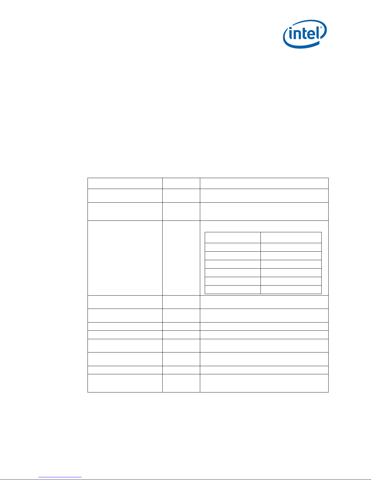
1.1 Terminology
Table 1. Terminology (Sheet 1 of 2)
Term Definition
A “#” sy mbo l afte r a s ig na l na me r ef e rs to an ac ti v e lo w si gn al, i ndi ca ti n g a s ig na l i s in
the active state when driven to a low level. For example, when RESET# is low, a reset
has been requested. Conversely, when NMI is high, a non-maskable interrupt has
#
AGTL+
Front Side Bus (FSB)
GTLREF
MT/s Megatransfers/second
Overshoot
Pad
Processor A single package that contains one complete execution core
occurred. In the case of signals where the name does not imply an active state but
describes part of a binary sequence (such as address or data), the “#” symbol implies
that the signal is inverted. For example, D[3:0] = “HLHL” refers to a hex ‘A ’, and
D[3:0]# = “LHLH” also refers to a hex “A” (H= High logic level, L= Low logic level).
XXXX means that the specification or value is yet to be determined.
Advanced Gunning Tran sceiver Logic. Used to refer to Assisted GTL+ signaling
technology on the processor
The electrical interface that connects the processor to the chipset. Also referred to as
the processor system bus or the system bus. All memory and I/O transactions as well
as interrupt messages pass between the processor and chipset over the FSB.
A reference voltage level used on the system bus to determine the logical state of a
signal.
The maximum voltage observed for a signal at the device pad, measured with
respect to the buff er ref ere nc e volta ge.
The electrical contact point of a semiconductor die to the package substrate. A pad is
only observable in simulations.
January 2007 DS
Order Nu mber: 315876 - 00 2 7
Intel® Celeron® Process or 1.66 GHz/1.83 GHz
Page 8
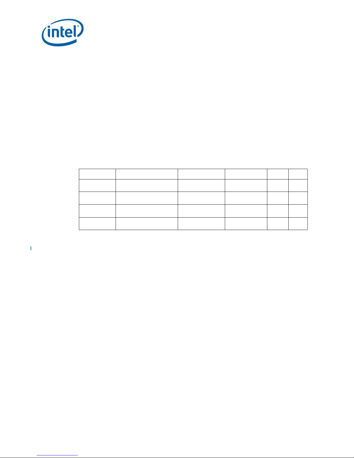
Table 1. Terminology (Sheet 2 of 2)
Term Definition
Ringback
Undershoot The minimum voltage extending below VSS observed for a signal at the device pad.
VRD
The voltage to which a sign al transition s to just after reaching its maxi mum
absolute value. Ringback may be caused by reflections, driver oscillations, or
other transmission line phenomena.
Voltage Regulator-Down for the processor that supplies the required voltage and
current to a single processor.
1.2 References
Material and concepts available in the following documents may be beneficial when
reading this document.
Table 2 . References
Dual-Core Intel® Xeon® Processor LV and ULV Specification Update
®
Intel
E7520 Me mory Controller Hub (M CH ) Datas heet
®
Intel
6300ESB I/O Controller Data sheet
Embedded Voltage Regulator-Down (EmVRD) 11.0 Design Guidelines for Embedded
Implementations Supporting PGA478
®
Intel
Celeron® Processor 1.66 GHz/1.83 GHz Thermal Design Guideline for
Embedded Applications
®
Intel
64 and IA-32 Architectures Software Developer's Manuals
Volume 1: Basic Architecture 253665
Volume 2A/2B: Instruction Set Reference
Volu me 3A/3B: System P rogrammin g Guide
®
Intel
Processor Identification and CPUID Instruction application note (AP-485)
1. Order numbers are subject to change
Intel® Celeron® Processor 1.66 GHz/1.83 GHz—Introduction
Document Order Number
http://www.intel.com/
design/intarch/
specupdt/311392.htm
ftp://
download.intel.com/
design/chipsets/
datashts/
30300602.pdf
http://
developer.intel.com/
design/intarch/
datashts/300641.htm
http://
developer.intel.com/
design/intarch/
designgd/311395.htm
http://
developer.intel.com/
design/intarch/
designgd/315745.pdf
http://
developer.intel.com/
design/pentium4/
manuals/
index_new.htm
253666
253667
253668
253669
http://www.intel.com/
support/processors/sb/
cs-009861.htm
1
®
Celero n® Processor 1.66 GHz/1. 83 GHz
Intel
DS January 2007
8 Order Nu mber: 315876 - 00 2
Page 9

Introduction—Intel
®
Celeron® Processor 1.66 GHz/1.83 GHz
1.3 State of Data
The data contained within this document represents the most accurate information
available by the publication date.
Note: All references to the Intel
apply to the Intel
®
Celeron® Processor 1.66 GHz/1.83 GHz only, unless otherwise
specified.
®
Celeron® Processor 1.66 GHz/1.83 GHz in this document
January 2007 DS
Order Nu mber: 315876 - 00 2 9
Intel® Celeron® Process or 1.66 GHz/1.83 GHz
Page 10
Intel® Celeron® Processor 1.66 GHz/1.83 GHz—Low Power Features
2.0 Low Power Features
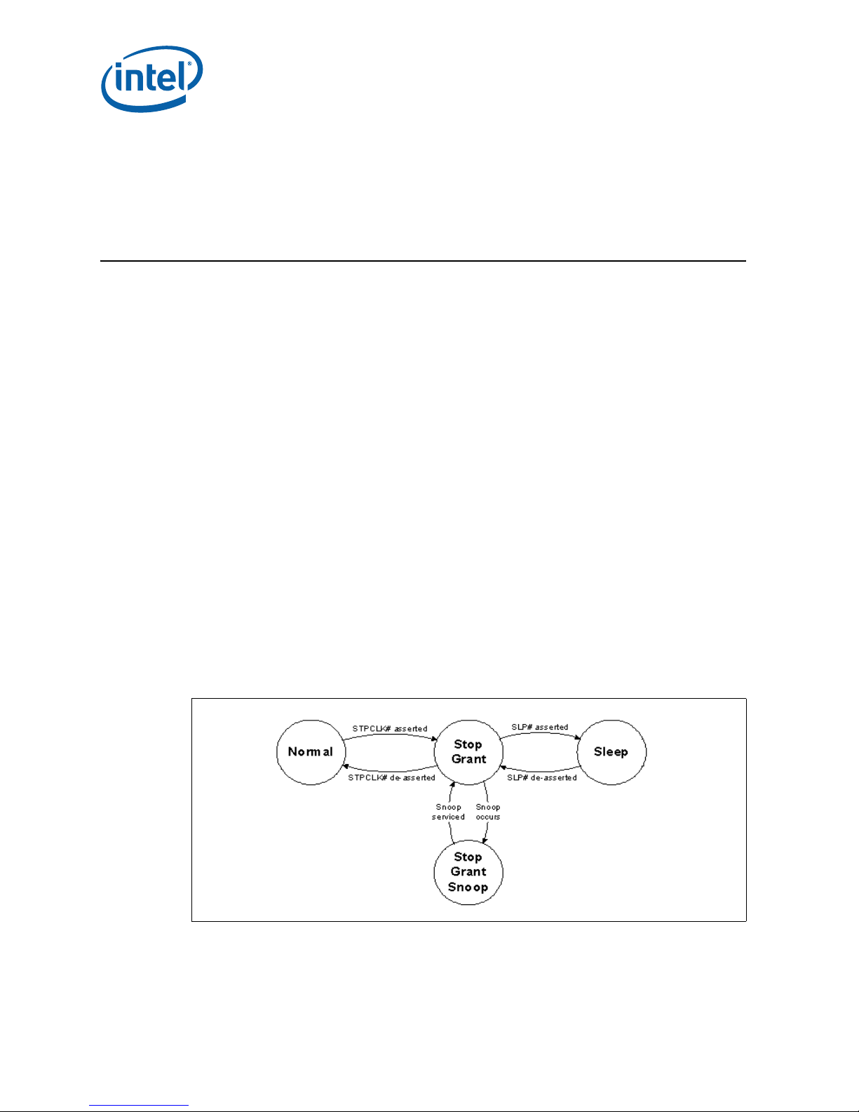
2.1 Clock Control and Low Power States
The Intel® Celeron® Processor 1.66 GHz/1.83 GHz supports the C1/AutoHALT, C1/
MWAIT, S top G r an t a nd Sl eep s ta tes f or op tima l powe r mana ge men t. C1/ Aut oHALT and
C1/MWAIT are core-level low power states only, they do not have package-level
behavior. Refer to Figure 1 for a visual representation of package level low-power
states for a Intel
Celeron
®
Processor 1.66 GHz/1.83 GHz can enter the C1/AutoHALT/MWAIT at any
time.
Refer to Figure 2 for a visual representation of the core low-power states for the Intel
Celeron
Intel
®
Processor 1.66 GHz/1.83 GHz.
®
Celeron® Processor 1.66 GHz/1.83 GHz implements two software interfaces for
requesting low power states: the I/O mapped ACPI P_BLK register block and the Cstate extens io n to the MW AI T in stru ction . Ei th er int erf ace can b e use d at a ny ti me. The
processor core presents an independent low power state request interface (ACPI P_BLK
or MWAIT). Requests from the software running on the core puts into core-level low
power state. The processor has logic for coordinating low power state requests from
the processor core. This logic puts the Intel
into a package-level low-power state based on the highest core low power state, as
desired.
®
Celeron® Processor 1.66 GHz/1.83 GHz. The single core Intel®
®
Celeron® Processor 1.66 GHz/1.83 GHz
®
If the core encounters a break event while STPCLK# is asserted, it returns to C0 state
by asserting the PBE# output signal. PBE# assertion signals to system logic that the
processor needs to return to the Normal package-level state. This allows that core to
return to the C0 state.
Figure 1. Package-Level Low Power States
®
Celeron® Processor 1.66 GHz/1.83 GHz
Intel
DS January 2007
10 Order Nu mber: 315876 - 00 2
Page 11
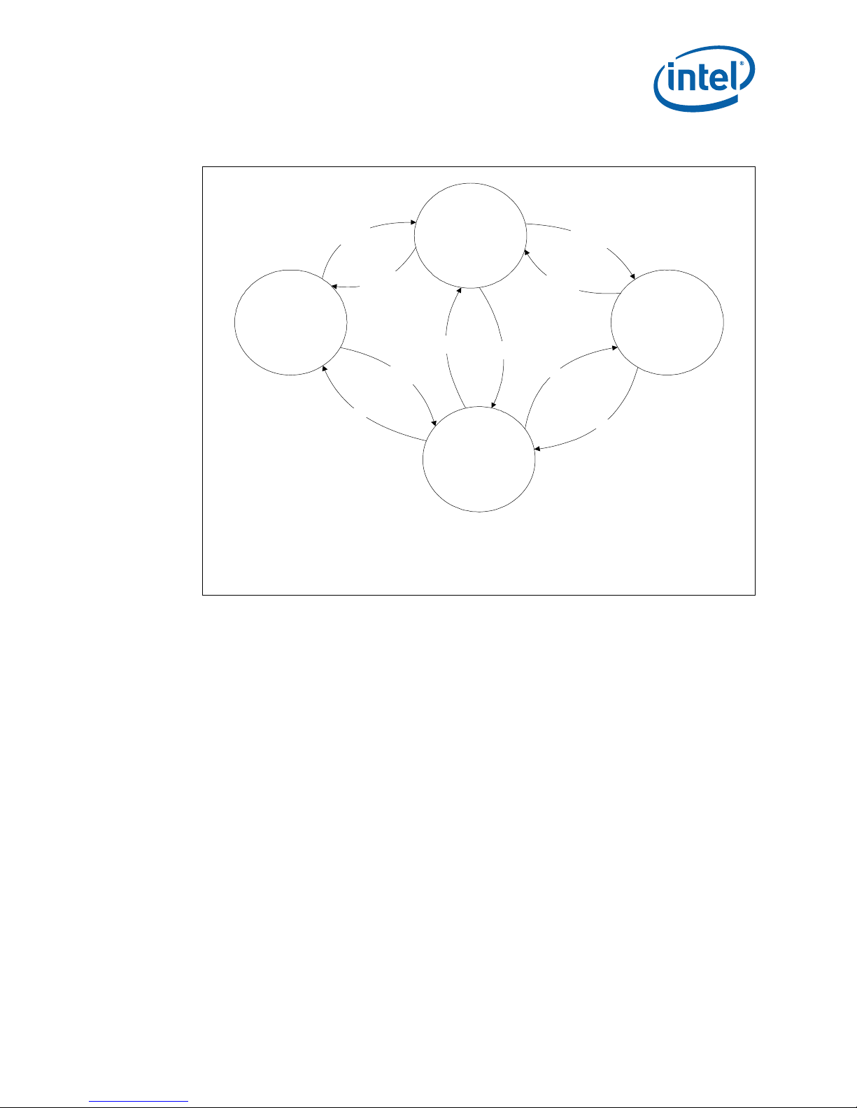
Low Power Features—I ntel
®
Celeron® Processor 1.66 GHz/1.83 GHz
Figure 2. Core Low Power States
STPCLK#
asserted
STPCLK#
de-asserted
C1/
MWAIT
Core state break
or MONITOR
MWAIT(C1)
halt br eak = A20M # transition, INIT# , INTR, NMI, PREQ #, RESET#, SMI#, or APIC interrupt
core state br eak = (halt break OR MON IT OR event) AND STPCLK# high (not asserted)
2.1.1 Core Low Power States
STPCLK#
asserted
Stop
Grant
STPCLK#
de-asserted
C0
STPCLK#
asserted
HLT instruction
STPCLK#
de-asserted
Halt break
C1/Auto
Halt
2.1.1.1 C0 State - Normal State
This is the normal operating state for the processor.
2.1.1.2 C1/AutoHALT Powerdown State
AutoHALT is a low power state entered when the processor executes the HALT
instruction. The processor transitions to the Normal state upon the occurrence of SMI#,
BINIT#, INIT#, LINT[1:0] (NMI, INTR), or an interrupt delivered over the system bus.
RESET# causes the processor to immediately initialize itself.
The return from a System Management Interrupt (SMI) handler can be to either
Normal Mode or the AutoHALT Power Down state. Refer to the Intel® 64 and IA-32
Architectures Software Developer's Manuals in Volume 3A/3B: System Programming
Guide for more information.
The system can generate a STPCLK# while the processor is in the AutoHALT Power
Down state. When the system deasserts the STPCLK# interrupt, the processor returns
execution to the HALT state.
While in AutoHALT Power Down state, the processor continues to processes system bus
snoops.
January 2007 DS
Order Nu mber: 315876 - 00 2 11
Intel® Celeron® Process or 1.66 GHz/1.83 GHz
Page 12

Intel® Celeron® Processor 1.66 GHz/1.83 GHz—Low Power Features
2.1.1.3 C1/MWAIT Powerdown State
MWAIT is a low power state entered when the processor core executes the MWAIT
instruction. Processor behavior in the MWAIT state is identical to the AutoHALT state
except that there is an addi tional event that can cause the processor core to return to
the C0 state: the Monitor event. Refer to the Intel® 64 and IA-32 Architectures
Software Developer's Manuals in Volume 3A/3 B : Syst em Pro gra mm in g Guide for more
information.
2.1.2 Packag e L o w Power States
The following sections describe all package level low power states for the Intel®
Celeron
®
Processor 1.66 GHz/1.83 GHz.
2.1.2.1 Normal State
This is the normal operating state for the processor. Intel® Celeron® Processor 1.66
GHz/1.83 GHz en te rs the Norm al st ate wh en its core is in the Norm al , AutoH ALT, or
MWAIT state.
2.1.2.2 Stop-Grant State
When the STPCLK# pin is asserted, the Stop-Grant state of the processor is entered 20
bus clocks after the response phase of the processor-issued Stop Grant Acknowledge
special bus cycle. Once the STPCLK# pin has been asserted, the Intel
Processor 1.66 GHz/1.83 GHz, the processor core must be in the Stop Grant state
before the deassert ion of STPCLK #.
Since the AGTL+ signal pins receive power from the system bus, these pins should not
be driven (allowing the level to return to V
termination resistors in this state. In addition, all other input pins on the system bus
should be driven to the inactive state.
BINIT# is not serviced while the processor is in Stop-Grant state. The event is latched
and can be serviced by software upon exit from the Stop Grant state.
RESET# causes the processor to immediately initialize itself, but the processor stays in
Stop-Grant state. A transition back to the Normal state occurs with the de-assertion of
the STPCLK# signal. When re-entering the Stop-Grant state from the Sleep state,
STPCLK# should only be deasserted one or more bus clocks after the deassertion of
SLP#.
®
Celeron®
) for minimum power drawn by the
CCP
A transition to the HALT/Grant Snoop state occurs when the processor detects a snoop
on the system bus A transiti on to the Sle ep sta te occ urs with the asse rti on of the SLP#
signal.
While in the Stop-Grant state, SMI#, INIT#, BINIT# and LINT[1:0] is latched by the
processor, and only serviced when the processor returns to the Normal state. Only one
occurrence of each event is recognized upon return to the Normal state.
While in Stop-Grant state, the processor processes snoops on the system bus and it
latches interrupts delivered on the system bus.
The PBE# signal can be driven when the processor is in Stop-Grant state. PBE# is
asserted if there is any pending interrupt latched within the processor. Pending
interrupts that are blocked by the EFLAGS.IF bit being clear still causes assertion of
PBE#. As serti on of PBE # indica tes to sy stem lo gic that it shou ld ret urn the proce ssor to
the Normal state .
®
Celeron® Processor 1.66 GHz/1.83 GHz
Intel
DS January 2007
12 Order Nu mber: 315876 - 00 2
Page 13

Low Power Features—I ntel
®
Celeron® Processor 1.66 GHz/1.83 GHz
2.1.2.3 Stop Grant Snoop State
The processor responds to snoop or interrupt transactions on the FSB while in StopGrant state. During a snoop or interrupt transaction, the processor enters the Stop
Grant Snoop state. The processor stays in this state until the snoop on the FSB has
been serviced (whether by the processor or another agent on the FSB) or the interrupt
has been latched. After the snoop is serviced or the interrupt is latched, the processor
returns to the Stop-Grant state.
2.1.2.4 Sleep State
The Sleep state is a very low power state in which the processor maintains its context,
maintains the phase-locked loop (PLL), and has stopped most of internal clocks. The
Sleep state can only be entered from Stop-Grant state. Once in the Stop-Grant state,
the processor enters the Sleep state upon the assertion of the SLP# signal. The SLP#
pin has a mini mum assert ion of one BCLK period. The SLP# pin sh ould only be asser ted
when the processor is in the Stop Grant state. For the Intel
GHz/1.83 GHz, the SLP# pin may only be asserted the processor core is in the StopGrant state. SLP# assertions while the processor is not in the Stop-Grant state are out
of specification and may results in illegal operation.
Snoop events that occur while in Sleep state or during a transition into or out of Sleep
state causes unpredictable behavior.
®
Celeron® Processor 1.66
In the Sleep state, the processor is incapable of responding to snoop transactions or
latching interrupt signals. No transitions or assertions of signals (with the exception of
SLP# or RESET#) are allowed on the system bus while the processor is in Sleep state.
Any transition on an input signal before the processor has returned to Stop-Grant state
results in unpredictable behavior.
If RESET# is driven active while the processor is in the Sleep state, and held active as
specified in the RESET# pin specification, then the processor resets itself, ignoring the
transiti on through Sto p-Gran t state. If RESET # is driven acti ve while the processor i s in
the Sleep state, the SLP# and STPCLK# signals should be deasserted immediately after
RESET# is asserted to ensure the processor correctly executes the reset sequence.
When the processor is in Sleep state, it does not respond to interrupts or snoop
transactions.
2.2 Enhanced Intel® SpeedStep® Technology (EIST)
Intel® Celeron® Processor 1.66 GHz/1.83 GHz does not support this feature.
2.3 Extended Halt State (C1E)
The Intel® Celeron® Processor 1.66 GHz/1.83 GHz Extended Halt State (C1E) enables
significant power savings. Extended HALT state is a low power state entered when the
processor core has executed the HALT or MWAIT instructions and Extended HALT state
has been enabled via the BIOS. When the processor core executes the HALT
instruction, the core is halted. The Extended HALT state is a lower power state than the
HALT state or Stop Grant state.
Note: The Extended HALT (C1E) state must be enabled for the processor to remain within its
specifications.
The Extended HALT state requires support for dynamic VID transitions in the platform.
The processor a utomati cally tr ansiti ons to a l ower core frequenc y and vo ltage oper ating
point before entering the Extended HALT state. Note that the processor FSB frequency
January 2007 DS
Order Nu mber: 315876 - 00 2 13
Intel® Celeron® Process or 1.66 GHz/1.83 GHz
Page 14

Intel® Celeron® Processor 1.66 GHz/1.83 GHz—Low Power Features
is not altered; only the internal core frequency is changed. When entering the low
power state, the processor first switches to the lower bus to core frequency ratio and
then transition to the lower voltage (VID).
While in the Extended HALT(C1E) state, the processor processes bus snoops. The
processor exits the Extended HALT state when a break event occurs. When the
processor e xi ts the E x tend ed HA LT state, it f irst transitions the VID to th e or igina l value
and then changes the bus to core frequency ratio back to the original value.
®
Celeron® Processor 1.66 GHz/1.83 GHz
Intel
DS January 2007
14 Order Nu mber: 315876 - 00 2
Page 15

Electrical Specifications—Intel
®
Cele r o n® Proc essor 1.66 G Hz/1.83 GHz
3.0 Electrical Specifications
3.1 Front Side Bus and GTLREF
Most Inte l® Celeron® Processor 1.66 GH z/1.8 3 GH z F SB si gn als use Ad v an ced Gu nni ng
Transceiver Logic (AGTL+) signalling technology. This signalling technology provides
improved noise margins and reduced ringing through low-voltage swings and controlled
edge rates. The termination voltage level for the Intel
1.83 GHz AGTL+ signals is V
data and address bus, signal integrity and platform design methods have become more
critical than with previous processor families.
The AGTL+ inputs require a reference voltage (GTLREF) that is used by t he receivers t o
determine if a signal is a logical 0 or a logical 1. GTLREF must be generated on the
system board. Termination resistors are provided on the processor silicon and are
terminated to its I/O voltage (V
The AGTL+ bus depends on incident wave switching. Therefore, timing calculations for
AGTL+ signals are based on flight time as opposed to capacitive deratings. Analog
signal simulation of the FSB, including trace lengths, is highly recommended when
designing a system.
= 1.05 V (nominal). Due to speed improvements to
CCP
).
CCP
®
Celeron® Processor 1.66 GHz/
3.2 Power and Ground Pins
For clean, on-chip power distribution, the Intel® Celeron® Processor 1.66 GHz/1.83
GHz has a large num ber of V
connected to V
power planes while all VSS pins must be connected to system ground
CC
(power) and V
CC
planes. Use of multiple power and ground planes is recommended to reduce IR drop.
The processor V
(Voltage ID) pins.
pins must be supplied with the voltage determined by the VID
CC
3.3 Decoupling Guidelines
Due to its large number of transistors and high internal clock speeds, the processor is
capable of generating large average current swings between low and full power states.
This may cause voltages on power planes to sag below their minimum values if bulk
decoupling is not adequate. Care must be taken in the board design to ensure that the
voltage provided to the processor remains within the specifications listed in Table 7.
Failure to do so can result in timing violations or reduced lifetime of the component.
3.3.1 V
Decoupling
CC
Regulator solutions need to provide bulk capacitance with a low effective series
resistance (ESR) and keep a low interconnect resistance from the regulator to the
socket. Bulk decoupling for the large current swings when the part is powering on, or
entering/exiting low-power states, must be provided by the voltage regulator solution.
For more details on decoupling recommendations, please refer to the Embedded
Voltage Regulator-Down (EmVRD) 11.0 Design Guidelines for Embedded
Implementations Supporting PGA478.
(ground) inputs. All power pins must be
SS
January 2007 DS
Order Nu mber: 315876 - 00 2 15
Intel® Celeron® Process or 1.66 GHz/1.83 GHz
Page 16
Intel® Celeron® Processor 1.66 GHz/1.83 GHz—Electrical Specifications
3.3.2 FSB AGTL+ Decoupling
The processor integrates signal termination on the die as well as incorporate high
frequency decoupling capacitance on the processor package. Decoupling must also be
provided by the system motherboard for proper AGTL+ bus operation.
3.3.3 FSB Cloc k ( B C LK [ 1 :0]) and Pro c es sor Clocking
BCLK[01:00] directly controls the FSB interface speed as well as the core frequency of
the processor. As in previous generation processors, the Intel
1.66 GHz/1.83 GHz core frequency is a multiple of the BCLK[01:00] frequency. The
®
Intel
Celeron® Processor 1.66 GHz/1.83 GHz bus ratio multiplier is set at its default
®
Celeron® Processor
ratio at manufacturing. The processor uses a differential clocking implementation.
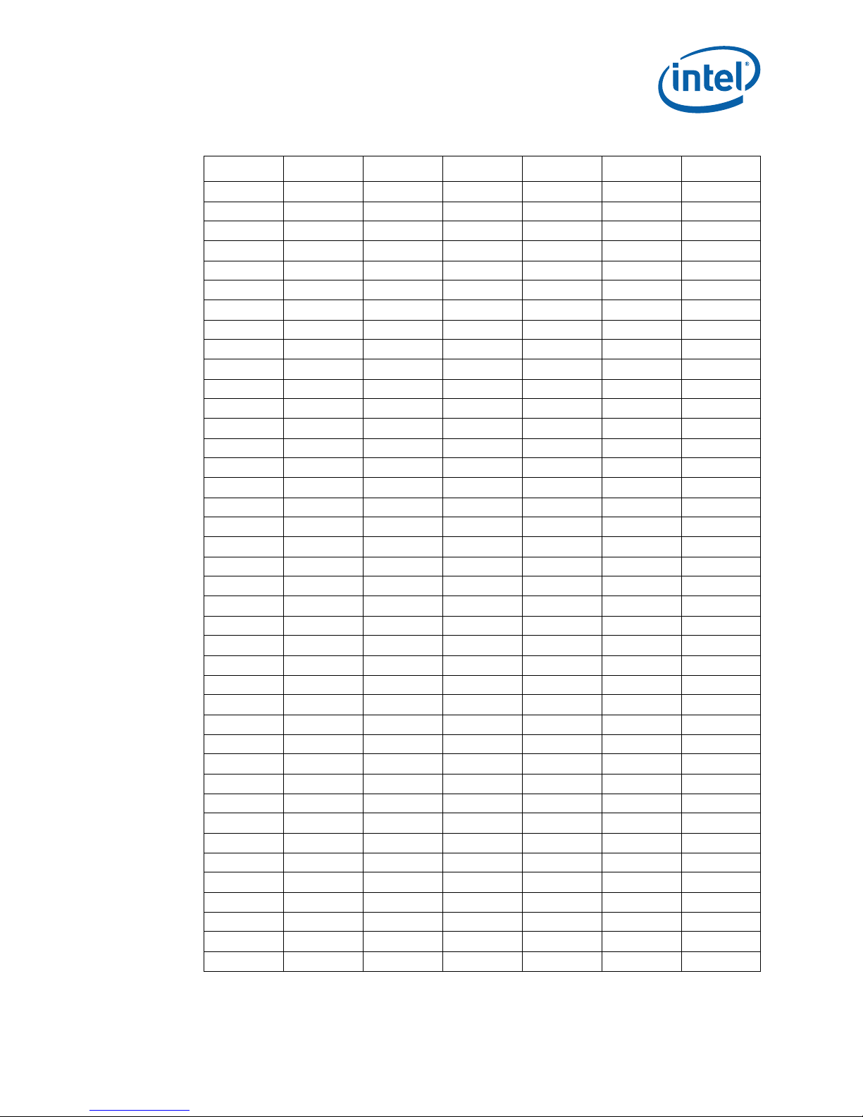
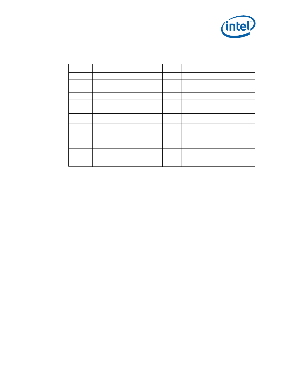
3.4 Voltage Identification and Power Sequencing
The VID specification for the Intel® Celeron® Processor 1.66 GHz/1.83 GHz is defined
by the Embedded Voltage Regulator-Down (EmVRD) 11.0 Design Guidelines for
Embedded Implementations Supporting PGA478.
The Intel
VID[5:0], to support automatic selection of power supply voltages. The VID pins for
Intel
processor VID circuitry. Table 3 specifies the voltage level corresponding to the state of
VID[5:0]. A ‘1’ in this refers to a high-voltage level and a 0 refers to low-voltage level.
For more details about VR design to support the Intel
1.83 GHz power supply requirements, please refer to the Embedde d Vo ltage Regulat or-
Down (EmVRD) 11.0 Design Guidelines for Embedded Implementations Supporting
PGA478.
Power source characteristics must be stable whenever the supply to the voltage
regulator is stable.
Table 3 . Intel
®
Celeron® Processor 1.66 GHz/1.83 GHz uses six voltage identification pins,
®
Celeron® Processor 1.66 GHz/1.83 GHz are CMOS outputs driven by the
®
Celeron® Processor 1.66 GHz/
®
Celeron® Processor 1.66 GHz/1.83 GHz VID Map (Sheet 1 of 3)
VID5 VID4 VID3 VID2 VID1 VID0 VCC (V)
000000OFF
0000011.6000
0000101.5875
0000111.5750
0001001.5625
0001011.5500
0001101.5375
0001111.5250
0010001.5125
0010011.5000
0010101.4875
0010111.4750
0011001.4625
0011011.4500
0011101.4375
0011111.4250
®
Celero n® Processor 1.66 GHz/1. 83 GHz
Intel
DS January 2007
16 Order Nu mber: 315876 - 00 2
Page 17
Electrical Specifications—Intel
®
Cele r o n® Proc essor 1.66 G Hz/1.83 GHz
Table 3. Inte l® Celeron® Processor 1.66 GHz/1.83 GHz VID Map ( Sheet 2 of 3)
VID5 VID4 VID3 VID2 VID1 VID0 VCC (V)
0100001.4125
0100011.4000
0100101.3875
0100111.3750
0101001.3625
0101011.3500
0101101.3375
0101111.3250
0110001.3125
0110011.3000
0110101.2875
0110111.2750
0111001.2625
0111011.2500
0111101.2375
0111111.2250
1000001.2125
1000011.2000
1000101.1875
1000111.1750
1001001.1625
1001011.1500
1001101.1375
1001111.1250
1010001.1125
1010011.1000
1010101.0875
1010111.0750
1011001.0625
1011011.0500
1011101.0375
1011111.0250
1100001.0125
1100011.0000
1100100.9875
1100110.9750
1101000.9625
1101010.9500
1101100.9375
1101110.9250
January 2007 DS
Order Nu mber: 315876 - 00 2 17
Intel® Celeron® Process or 1.66 GHz/1.83 GHz
Page 18
Intel® Celeron® Processor 1.66 GHz/1.83 GHz—Electrical Specifications
Table 3 . Intel® Celeron® Processor 1.66 GHz/1.83 GHz VID Map (Sheet 3 of 3)
VID5 VID4 VID3 VID2 VID1 VID0 VCC (V)
1110000.9125
1110010.9000
1110100.8875
1110110.8750
1111000.8625
1111010.8500
1111100.8375
1111110.8250
3.5 Catastrophic Thermal Protection
The Intel® Celeron® Processor 1.66 GHz/1.83 GHz supp orts the T HERMTRIP# s ignal for
catastrophic thermal protection. An external thermal sensor should also be used to
protect the processor and the system against excessive temperatures. Even with the
activation of THERMTRIP#, which halts all processor internal clocks and activity,
leakage current can be high enough such that the processor cannot be protected in all
conditions without the removal of power to the processor. If the external thermal
sensor detects a catastrophic processor temperature of approximately 125 °C
(maximum), or if the THERMTRIP# signal is asserted, the V
must be turned of f within 500 ms to prevent p ermanen t sil icon d amage due to therm al
runaway of the processor.
supply to the processor
CC
3.6 Signal Terminations and Unused Pins
All RSVD ( RES ERVE D) pi ns must r emai n unc onn ec ted. Conne c ti on of th es e pi ns t o VCC,
V
, or to any other signal (including each other) can result in component malfunction
SS
or incompatibility with future processors. See Table 15 for a pin listing of the processor
and the location of all RSVD pins.
For reliable operation, always connect unused inputs or bidirectional signals to an
appropriate signal level. Unused active low AGTL+ inputs may be left as no connects if
AGTL+ termination is provided on the processor silicon. Unused active high inputs
should be connected through a resistor to ground (V
unconnected.
). Unused outputs can be left
SS
Note: The TEST1 and TEST2 pins have unique signal termination requirements. It is
mandatory that the TEST2 pin have a 51 Ω +/-5% pull down resistor to V
refer to Table 11 for details.
. Please
SS
3.7 FSB Frequency Select Signals (BSEL[2:0])
The BSEL[2:0] signals are used to select the frequency of the processor input clock
(BCLK[1:0]). The BSEL encoding for BCLK[1:0] is shown in Table 4.
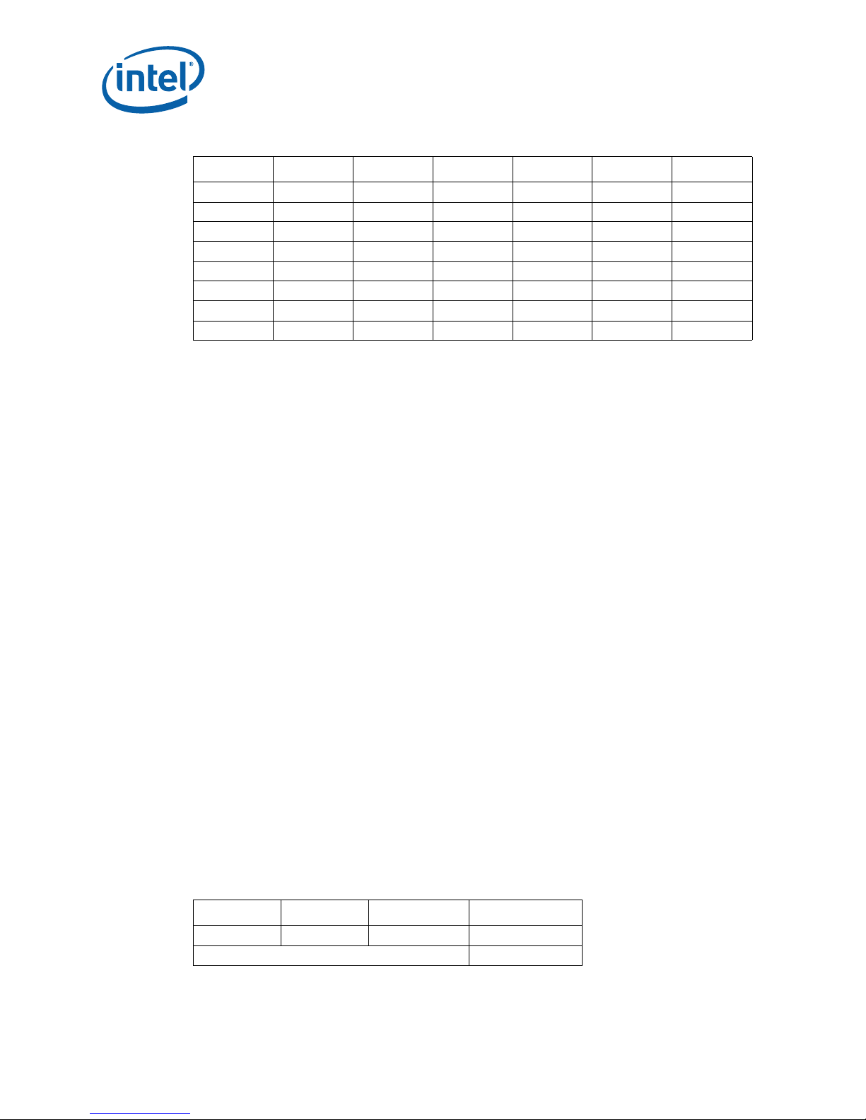
Table 4. BSEL[2:0] Encoding for BCLK Frequency
BSEL[2] BSEL[1] BSEL[0] BCLK frequency
LHH 166MHz
All other combinations RESERVED
®
Celero n® Processor 1.66 GHz/1. 83 GHz
Intel
DS January 2007
18 Order Nu mber: 315876 - 00 2
Page 19
Electrical Specifications—Intel
®
Cele r o n® Proc essor 1.66 G Hz/1.83 GHz
3.8 FSB Signal Groups
In order to simplify the following discussion, the FSB signals have been combined into
groups by buffer type. AGTL+ input signals have differential input buffers, which use
GTLREF as a reference level. In this document, the term "AGTL+ Input" refers to the
AGTL+ input group as well as the AGTL+ I/O group when receiving. Similarly, "AGTL+
Output" refers to the AGTL+ output group as well as the AGTL+ I/O group when
driving.
With the implementation of a source synchronous data bus comes the need to specify
two sets of timing parameters. One set is for common clock signals which are
dependant upon the rising edge of BCLK0 (ADS#, HIT#, HITM#, etc.) and the second
set is for the source synchronous signals which are relative to their respective strobe
lines (data and address) as well as the rising edge of BCLK0. Asychronous signals are
still present (A20M#, IGNNE#, etc.) and can become active at any time during the
clock cycle. Ta ble 5 identifies which signals are common clock, source synchronous,
and asynch r ono u s.
Table 5. FS B Pin Groups
Signal Group Type Signals
AGTL+ Common Clock Input
AGTL+ Common Clock I/O
Synchronous
to BCLK[1:0]
Synchronous
to BCLK[1:0]
1
BPRI#, DEFER#, PREQ#, RESET#, RS[2:0]#, RSP#,
TRDY#
ADS#, AP[1:0]#,BINIT#, BNR#, BPM[3 :0]#
DBSY#, DP[3:0], DRDY#, HIT#, HI TM#, LOCK#,
MCERR#, PRDY#
3
3
, BR[0]#,
Signals Associ ated Strobe
REQ[4:0]#, A[16:3]# ADST B[0]#
AGTL+ Source Synchronous I/O
AGTL+ Strobes
CMOS Input Asynchronous
Open Drain Output Asynchronous FERR#, IERR#, THERMTRIP#, PROCHOT#
CMOS Outp ut Asynchr o no us VI D[5 : 0 ], BSE L[ 2 :0 ]
CMOS Input
Open Drain Output
FSB Clock Clock BCLK[1:0]
Power/Other
Notes:
1. Refer to Chapter 4.0 for signal descriptions and termination requirements.
2. BPM[2:1]# and PRDY# are AGTL+ output only signals.
Synchronous
to assoc.
strobe
Synchronous
to BCLK[1:0]
Synchronous
to TCK
Synchronous
to TCK
A[35:17]# ADSTB[1]#
D[15:0 ]# , DIN V 0 # DSTBP0# , DST BN 0#
D[31:16]#, DINV1# DSTBP1#, DSTBN1#
D[47:32]#, DINV2# DSTBP2#, DSTBN2#
D[63:48]#, DINV3# DSTBP3#, DSTBN3#
ADSTB[1:0]#, DSTBP[3:0]#, DSTBN[3:0]#
A20M#, FORCEPR#, IGNNE#, INIT#, LINT0/INTR, LINT1/
NMI, PWRGOOD, SMI#, SLP#, STPCLK#
TCK, TDI, TMS, TRST#
TDO
COMP[3:0], DBR#
THERMDA, THERMDC, ODTEN, V
V
SS, VSS_SENSE
2
, GTLREF, RSVD, TEST2, TEST1,
, V
, V
CC
CCA
CCP , VCC_SENSE
,
January 2007 DS
Order Nu mber: 315876 - 00 2 19
Intel® Celeron® Process or 1.66 GHz/1.83 GHz
Page 20
Intel® Celeron® Processor 1.66 GHz/1.83 GHz—Electrical Specifications
3.9 CMOS Signals
CMOS input signals are shown in Table 5. Legacy output FERR#, IERR# and other nonAGTL+ signals (THERMTRIP# and PROCHOT#) utilize Open Drain output buffers. These
signal s do not ha v e se tu p o r ho ld ti m e sp ec if icat io ns in rel a tion t o BCL K[ 1:0] . Howe ve r,
all of the CMOS signals are required to be asserted for at least three BCLKs in order for
the processor to recognize them. See Section 3.11 for the DC for the CMOS signal
groups.
3.10 Maximum Ratings
Table 6 lists the processor’s maximum environmental stress ratings. The processor
should not receive a clock while subjected to these conditions. Extended exposure to
the maximum ratings may affect device reliability . Furthermore, although the processor
contains protective circuitry to resist damage from Electro-Static Discharge (ESD), one
should always take precautions to avoid high static voltages of electric fields.
Table 6. Processor DC Absolute Maximum Ratings
Symbol Parameter Min Max Unit Notes
STORAGE
T
V
CC
V
inAGTL+
V
inAsynch_CMOS
Notes:
1. For functional operation, all processor electrical, signal quality, mechanical and thermal specifications
2. Excessive overshoot or undershoot on any signal will likely result in permanent damage to the
3. Storage temperature is applicable to storage conditions only. In this scenario, the processor must not
must be satisfied.
processor .
receive a clock, and no pins can be connected to a voltage bias. Storage within these limits will not
affect the long term reliability of the device. For functional operation, please refer to the processor
case temperature specificat ions.
Processor storage
temperature
Any processor supply
voltage with respect to V
AGTL+ buffer DC input
voltage with respect to V
CMOS buffer DC input
voltage with respect to V
SS
SS
SS
-40 85 °C 2
-0.3 1.6 V 1
-0.1 1.6 V 1, 2
-0.1 1.6 V 1, 2
3.11 Processor DC Specifications
Note: Th e p roce s sor DC sp e ci fi cations in this se cti on are de fin ed at the processor core (pa ds )
®
Celero n® Processor 1.66 GHz/1. 83 GHz
Intel
DS January 2007
20 Order Nu mber: 315876 - 00 2
unless noted otherwise.
See Table 5 for the pin signal definitions and signal pin assignments. Most of the signals
on the FSB are in the AGTL+ signal group. The DC specifications for these signals are
listed in Table 8. DC specifications for the CMOS group are listed in Table 9.
Table 7 through Table 10 list the DC specifications for the Intel
1.66 GHz/1.83 GHz and are valid only while meeting specifications for junction
temperature, clock frequency, and input voltages. The Highest Frequency Mode (HFM)
and Lowest Frequency Mode (LFM) refer to the highest and lowest core operating
frequencies supported on a particular processor. Active mode load line specifications
apply in all states. V
power up in order to set the VID values. Unless specified otherwise, all specifications
for the Intel
®
Celeron® Processor 1.66 GHz/1.83 GHz are at Tjunction = 100 °C. Care
should be taken to read all notes associated with each parameter.
The Intel
SpeedStep
®
Celeron® Processor 1.66 GHz/1.83 GHz does not support Enhanced Intel
®
Technology (EIST), therefore HFM and LFM transitions are not supported.
CC,BOOT
®
Celeron® Process o r
is the default voltage driven by the voltage regulator at
Page 21
Electrical Specifications—Intel
®
Cele r o n® Proc essor 1.66 G Hz/1.83 GHz
Table 7. Voltage and Current Specifications for the Intel® Celeron® Processor 1. 66
GHz/1.83 GHz
Symbol Parameter Min Typ Max Unit Notes
V
CC
V
CC,BOOT
V
CCP
V
CCA
I
CCDES
I
CC
I
AH,
I
SGNT
I
SLP
dI
CC/DT
I
CCA
I
CCP
Notes:
1. These are VID values. Individual processor VID values may be calibrated during manufacturing such
2. The voltage specifications are assumed to be measured across V
3. Specified at 100 C T
4. Specified at the VID voltage.
5. The I
6. Based on simulations and averaged over the duration of any change in current. Specified by design/
7. Refer to Figure 3 for a waveform illustration of this parameter.
8. Measured at the bulk cap acitors o n the motherboard.
9. V
10. I
11. Specified at the nominal voltage based on the loadline slope.
VCC CPU Core Voltage 1.1125 1.275 V 1, 2
Default V
Voltage for initial power up 1.1 V 2, 7, 9
CC
AGTL+ Termination Voltage 0.997 1.05 1.102 V 2
PLL supply voltage 1.425 1.5 1.575 V 2
ICC for Intel® Celeron® Process o r 1. 66
GHz/1.83 GHz Recommended Design
36 A 5
Target
ICC for Intel® Celeron® Process o r 1. 66
GHz/1.83 GHz
34 A 3,11
ICC Auto-Halt & Stop-Grant 23.2 A 3,4
I
SLP
V
power supply current slew rate 600 A/us 6, 8
CC
ICC for V
ICC for V
for V
I
CC
supply 120 mA
CCA
supply before V
CCP
supply after V
CCP
CC
CC
stable
stable
23.2 A 3,4
6.0
2.5
A10
that two devices at the same speed may have different VID settings. Actual voltage supplied to the
processor should be as specified in the load lines in Figure 3. Adherence to load line specifications is
required to ensure reliable processor operation. Note that this differs from the VID employed by the
processor during a power management event (Thermal Monitor 2 or Extended Halt State).
with a 100 MHz bandwidth oscilloscope, 1.5 pF maximum probe capacitance, and 1-Mohm minimum
impedance. The maximum length of grou nd wire on the prob e should be less than 5 mm. Ensure
external noise from the system is not coupled in the scope probe.
(max) specification comprehends only Intel® Celeron® Processor 1.66 GHz/ 1.83 GHz HFM
CCDES
frequencies. Platforms should be designed to this specification.
characterization at nominal V
, boot tolerance is shown in Figure 3.
CC
specification refers to the processor package on the front side bus.
CCP
.
J
. Not 100% tested.
CC
CCSENSE
and V
SSSENSE
pins at socket
January 2007 DS
Order Nu mber: 315876 - 00 2 21
Intel® Celeron® Process or 1.66 GHz/1.83 GHz
Page 22

Intel® Celeron® Processor 1.66 GHz/1.83 GHz—Electrical Specifications
]
Figure 3. Active VCC and ICC Load Line for Intel® Celeron® Process or 1.66 GHz/1.83 GHz
V
[V]
CC
Slope = -2.1 mV /A at package
VccSense, VssSense pins.
Differential Remote Sense required.
10mV= RIPPLE
V
CC, DC
V
CC, DC
max
V
CC
max
VCC nom
min
V
CC
min
+/-VCC nom * 1.5%
= VR St. Pt. Error
See Note
0
Note: Vcc > 0.82 50 V (VID 111 111)
.
Table 8. AGTL+ Signal Group DC Specifications (Sheet 1 of 2)
Symbol Parameter Min Typ Max Unit
V
CCP
GTLREF Reference Voltage 2/3 V
Notes:
1. Unless otherwise noted, all specifications in this table apply to all processor frequencies.
2. V
3. V
4. V
5. This is the pull down driver resistance. Refer to processor I/O Buffer Models for I/V characteristics.
6. GTLREF should be generated from V
7. R
8. Specified with on die R
9. Cpad includes die capacitance only. No package parasitics are included.
10. R
IL is defined as the maximum voltage level at a receiving agent that is interpreted as a logical low
value.
IH is defined as the minimum voltage level at a receiving agent that is interpreted as a logical high
value.
IH and VOH may experience excursions above V
the signal quality specifications.
Measured at 0.31*V
these specifications is the instantaneous V
is the on-die termination resistance measured at VOL of the AGTL+ output driver. Measured at
TT
0.31*V
characteristics.
for PREQ# is between 1.5kΩ and 6.0kΩ
TT
I/O V o ltage 1.00 1.05 1.10 V
-2% 2/3 V
CCP
. R
TT
. R
CCP
(min) = 0.38*R
ON
is connected to V
and R
TT
CCP
. However , input signal drivers must comply with
CCP
R
(typ) = 0.45*R
TT,
CCP
ON
.
with a 1% tolerance resistor divider. The V
CCP
on die. Refer to processor I/O buffer models for I/V
CCP
are turne d off.
ON
CCP
TT,
2/3 V
R
ON
ICC max
+2% V 6
CCP
(max) = 0.52*R
referred to in
CCP
ICC [A
Notes
TT.
1
®
Celero n® Processor 1.66 GHz/1. 83 GHz
Intel
DS January 2007
22 Order Nu mber: 315876 - 00 2
Page 23

Electrical Specifications—Intel
®
Cele r o n® Proc essor 1.66 G Hz/1.83 GHz
Table 8. AGTL+ Signal Group DC Specifications (Sheet 2 of 2)
VIH Input High Voltage GTLREF+100 V
IL Input Low Voltage -100 0 GTLREF-100 mV 2,4
V
VOH Output High Voltage V
R
Te rmination Resistance 45 50 55 Ω 7,10
TT
- 100 V
CCP
RON Buffe r On Resistance 22.3 25.5 28.7 W 5
ILI Input Leakage Current ± 100 µA 8
Cpad Pad Capacitance 1.8 2.3 2.75 pF 9
Notes:
1. Unless otherwise noted, all specifications in this table apply to all processor frequencies.
2. V
3. V
4. V
5. This is the pull down driver resistance. Refer to processor I/O Buffer Models for I/V characteristics.
6. GTLREF should be generated from V
7. R
8. Specified with on die R
9. Cpad includes die capacitance only. No package parasitics are included.
10. R
.
IL is defined as the maximum voltage level at a receiving agent that is interpreted as a logical low
value.
IH is defined as the minimum voltage level at a receiving agent that is interpreted as a logical high
value.
IH and VOH may experience excursions above V
the signal quality specifications.
Measured at 0.31*V
these specifications is the instantaneous V
is the on-die termination resistance measured at VOL of the A G TL+ out put driver. Mea sured at
TT
0.31*V
characteristics.
TT
. R
CCP
TT
for PREQ# is between 1.5kΩ and 6.0kΩ
. R
(min) = 0.38*R
CCP
ON
is connected to V
and R
TT
with a 1% tolerance resistor divider. The V
CCP
on die. Refer to processor I/O buffer models for I/V
CCP
are turned off.
ON
CCP
TT,
CCP
R
ON
.
CCP
. However, input signal drivers must comply with
(typ) = 0.45*R
Table 9. CMOS Signal Group DC Specifications
Symbol Parameter Min Typ Max Unit Notes
V
CCP
V
IL
IH Input High Voltage 0.7 1.05 1.20 V 2
V
VOL Output Low Voltage -0.1 0 0. 11 V 2
OH Output High Voltage 0.9 V
V
IOL Output Low Current 1.3 4.1 mA 4
IOH Output High Current 1.3 4.1 mA 5
I
LI
Cpad1 Pad Capacitance 1.8 2.3 2.75 pF 7
Cpad2
Notes:
1. Unless otherwise noted, all specifications in this table apply to all processor frequencies.
2. The V
3. Refer to the processor I/O Buffer Models for I/V characteristics.
4. Measured at 0.1*V
5. Measured at 0.9*V
6. For Vin between 0V and V
7. Cpad1 includes die capacitance only for PWRGOOD. No package parasitics are included.
8. Cpad2 includes die capacitance for all other CMOS input signals. No package parasitics are included.
I/O Voltage 0.997 1.05 1.102 V
Input Low Voltage
CMOS
-0.1 0 0.3 3 V 2, 3
CCP
Leakage Current ± 100 µA 6
Pad Capacitance for CMOS
Input
referred to in these specifications refers to instantaneous V
CCP
.
CCP
.
CCP
. Measured when the driv er is tristated.
CCP
0.95 1.2 1.45 pF 8
V
+100 mV 3,6
CCP
CCP
R
(max) = 0.52*R
TT,
ON
1.2 V 2
.
CCP
mV 6
TT.
referred to in
CCP
1
January 2007 DS
Order Nu mber: 315876 - 00 2 23
Intel® Celeron® Process or 1.66 GHz/1.83 GHz
Page 24

Intel® Celeron® Processor 1.66 GHz/1.83 GHz—Electrical Specifications
Table 10. Open Drain Signal Group DC Specifications
Symbol Parameter Min Typ Max Unit Notes
VOH Output High Voltage 1.0 1.05 1.10 V 3
VOL Output Low Voltage 0 0.20 V
IOL Output Low Current 11.4 50 mA 2
I
LEAK
Cpad Pad Capacitance 1.8 2.3 2.75 pF 5
Notes:
1. Unless otherwise noted, all specifications in this table apply to all processor frequencies.
2. Measured at 0.2 V
3. V
4. For Vin between 0 V and V
5. Cpad includes die capacitance only. No package parasitics are included.
Leakage Current ± 200 µA 4
is determined by value of the external pull-up resistor to V
OH
OH
.
CCP
1
.
®
Celero n® Processor 1.66 GHz/1. 83 GHz
Intel
DS January 2007
24 Order Nu mber: 315876 - 00 2
Page 25

Package Mechanical Specifications and Pin Information—Intel
1.83 GHz
®
Celeron® Processor 1.66 GHz/
4.0 Package Mechanical Specifications and Pin
Information
4.1 Package Mechanical Specifications
The Intel® Celeron® Processor 1.66 GHz/1.83 GHz is available in 478-pin Micro-FCPGA
(Micro- Flip Chip PGA) package.
4.1.1 Package Mechanical D r awings
Different views of the Micro-FCPGA package are shown in Figure 4, Figure 5, and
Figure 6.
Figure 4. Micro-FCPGA Pac k a ge Top and Bottom Views
January 2007 DS
Order Nu mber: 315876 - 00 2 25
Intel® Celeron® Process or 1.66 GHz/1.83 GHz
Page 26

Intel® Celeron® Processor 1.66 GHz/1.83 GHz—Package Mechanical Specifications and Pin
Figure 5. Micro-FCPGA Processor Package Drawing (Sheet 1)
Information
Note: All dimensions are in millimeters [inches]. Values shown for reference only.
®
Intel
Celero n® Processor 1.66 GHz/1. 83 GHz
DS January 2007
26 Order Nu mber: 315876 - 00 2
Page 27

Package Mechanical Specifications and Pin Information—Intel
1.83 GHz
®
Celeron® Processor 1.66 GHz/
Figure 6. Micro-FCPGA Processor Pack a ge Drawing (She et 2)
Note: All dimensions are in millimeters [inches]. Values shown for reference only.
4.1.2 Processor Component Keep-Out Zones
The processor may contain components on the substrate that define component keepout zone requi re ments. A the rmal and me chani cal sol uti on d esi gn m ust n ot in trud e i nto
the required keep-out zones. Decoupling capacitors are typically mounted in the keepout areas. The location and quantity of the capacitors may change, but remains within
the component keep-in. Refer to Figure 4, Figure 5, an d Figure 6 for keep-out zones.
January 2007 DS
Order Nu mber: 315876 - 00 2 27
Intel® Celeron® Process or 1.66 GHz/1.83 GHz
Page 28

Intel® Celeron® Processor 1.66 GHz/1.83 GHz—Package Mechanical Specifications and Pin
4.1.3 Package Loading Specifications
Maximum mechanical package loading specifications are given in Figure 5. These
specifications are static compressive loading in the direction normal to the processor.
This maximum load limit should not be exceeded during shipping conditions, standard
use condition, or by thermal solution. In addition, there are additional load limitations
against transient bend, shock, and tensile loading. These limitations are more platform
specific, and should be obtained by contacting your field support. Moreover, the
processor package substrate should not be used as a mechanical reference or loadbearing surface for thermal and mechanical solution.
4.1.4 Processor Mass Specifications
The typical mass of the processor is given in Figure 6. This mass includes all the
components that are included in the package.
4.2 Processor Pin-Out and Pin List
Figure 7 shows the top view pinout of the Intel® Celeron® Processor 1.66 GHz/1.83
GHz. The alphabetical pin listing is shown in Table 14. The alphabetical signal listing is
shown in Table 15.
Information
®
Intel
Celero n® Processor 1.66 GHz/1. 83 GHz
DS January 2007
28 Order Nu mber: 315876 - 00 2
Page 29

Package Mechanical Specifications and Pin Information—Intel
1.83 GHz
®
Celeron® Processor 1.66 GHz/
Figure 7. The Coordinates of the Processor Pins as Viewed From the Top of the Package
AF AE AD AC AB AA Y W V U T R P N M L K J H G F E D C B A
VID
SKT
1
[5]
OCC
VID
VID
2
[3]
[4]A[31]
VID
VID
3
[1]
[2]A[32]A[33]
PREQ#VID
4
5 VSS
6
BPM
[0]#
[0]
BPM
[3]#
VSS
7 VCC VCC VCC VCC
8 VSS VSS VSS VSS VSS VSS VSS VSS VSS VSS VSS VSS
9 VCC VCC VCC VCC VCC VCC VCC VCC VCC VCC VCC VCC
10 VCC VCC VCC VCC VCC VCC VCC VCC VCC VCC VCC VCC
11 VSS VSS VSS VSS VSS VSS VSS VSS VSS VSS VSS VSS
12 VCC VCC VCC VCC VCC VCC VCC VCC VCC VCC VCC VCC
A
VSS
[35]A[34]
VSS
VSS
A
[27]A[21]
VSS
[26]A[20]
VSS TDI TDO VSS
PRD
VSS TMS TCK VSS
Y#
BPM
[1]#
BPM
[2]#
VSS
VSS
SEN
TRS
T#
VCC
SEN
A
A
[29]A[30]
VSS
[28]A[25]
VSS
RSP#AP
[1]#
BINIT#AP
V
VSS V
CCP
A
VSS
[14]A[10]
VSS
A
[23]A[24]
VSS
[22]A[19]
VSS
[0]#
CCPVCCP
A
A
VSS
A
[13]A[12]
A
VSS
[16]A[9]#
VSS
A
RSV
[18]
D
ADSTBRSV
VSS
COMPCOMPA
VSS
[15]A[11]
VSS
[8]#
RSV
D
RSVDA[6]
VSS
A
A
[17]
ADSTBADS
VSS
D
VSS
BR0
#
VSS
A
VSS
[5]#A[4]#
REQ
[0]#A[7]#
VSS
#
MCE
VSS
RR#
BR1#BPRI
#
VSS
#
VSS
REQ
[3]#
HIT
M#
VSS
DEF
ER#
VSS
[3]#RS[0]#
REQ
REQ
[2]#
[4]#
REQ
VSS
[1]#
VSS
[2]#
TRDY#DRD
DBS
VSS
Y#
A
RS
Y#
VSS
RS
VSS
[1]#
BNR#HIT
LOC
VSS
K#
SMI#INIT
VSS
ODTENIGN
NE#
VCC VCC
#
RSVDRSV
D
RES
VSS
ET#
RSVDRSV
VSS
STP
RSVDLINT0PWR
CLK
VSS
#
A20M#LINT
VSS
RSVDSLP
#
RSVDFOR
CEP
VSS
D
GOO
FERR#THE
RMT
VSS
1
VCC VCC
13 VSS VCC VSS VCC VSS VCC VSS VCC VSS VCC VSS VCC
14 VCC VSS VCC VSS VCC VSS VCC VSS VCC VSS VCC VSS
15 VCC VCC VCC VCC VCC VCC VCC VCC VCC VCC VCC VCC
16 VSS VSS VSS VSS VSS VSS VSS VSS VSS VSS VSS VSS
17 VCC VCC VCC VCC VCC VCC VCC VCC VCC VCC VCC VCC
18 VCC VCC VCC VCC VCC VCC VCC VCC VCC VCC VCC VCC
19 VSS VSS VSS VSS VSS VSS VSS VSS VSS VSS VSS VSS
BSE
20 VCC VCC VCC VCC V
21 VSS V
22 V
CCPVCCP
23 V
CCP
24 VSS
25 V
CCP
26 V
CCP
CCPVCCP
VSS
[60]D[59]
RSV
VSS
D
D
VSS V
VSS V
D
V
[63]
VSS
VSS
[57]D[46]
GTL
REFD[58]
CCP
CCP
D
CCPVCCP
D
CCP
[62]
D
VSS
[61]
DINVD
VSS
D
[56]D[47]
VSS
D
VSS
[44]D[42]
DSTBPDST
VSS
D
[54]D[53]
VSS
[55]
D
VSS
[43]D[41]
D
[45]D[40]
VSS
VSS
BN
D
VSS
[48]D[49]
D
[51]D[52]
VSS
D
VSS
[38]D[39]
DINVD
[35]
DSTBPDST
BN
VSS
D
VSS
[37]D[32]D[31]
D
RSV
[50]
D
VSS
COMPCOMPD
VSS
VSS
D
[33]
VSS
DP
[2]#
DSTBPDST
BN
D
VSS
[24]D[15]
VSS
D
[36]DP[3]#
DP
VSS
[1]#D[30]
VSS
[34]
DSTBPDST
VSS
VSS
D
[14]D[12]
D
VSS
[25]D[26]
VSS
DP
[0]#D[28]
VSS
BN
D
[11]D[10]
D
VSS
[13]D[9]#
VSS
D
DIN
[29]
V
D
VSS
[27]D[22]
VCC VCC
D
[5]#D[2]#
D
VSS
[6]#D[3]#
VSS
D
[23]D[20]
D
VSS
[21]D[18]
VSS
VSS
D
[8]#D[7]#
VSS
D
[19]D[16]
L[1]
D
[0]#
VSS
D
[17]
VSS
BSE
L[0]
IERR
#
D
[1]#
VSS
DIN
V
D
[4]#
VSS
VCC VCC
BSE
VSS
L[2]
THR
THR
MDA
MDC
TEST2VCC
TES
VSS
T1
PRO
VSS
CHO
BCL
BCL
K[0]
K[1]
A
January 2007 DS
Order Nu mber: 315876 - 00 2 29
Intel® Celeron® Process or 1.66 GHz/1.83 GHz
Page 30

Intel® Celeron® Processor 1.66 GHz/1.83 GHz—Package Mechanical Specifications and Pin
4.2.1 Alphabet i c al Si g na l s Re fer ence
Table 11. Signal Description (Sheet 1 of 7)
Name Type Description
A[35:3]# (Address) define a 2
phase 1 of the address phase, these pins transmit the address of a transaction.
A[35:3]#
Input/
Output
A20M# Input
ADS#
Input/
Output
In sub-phase 2, these pins transmit transaction type information. These signals
must connect the appropriate pins of both agents on the Intel
Processor 1.66 GHz/1.83 GHz FSB. A[35:3]# are source synchronous signals
and are latched into the receiving buffers by ADSTB[1:0]#. Address signals are
used as straps which are sampled before RESET# is deasserted.
If A20M# (Address-20 Mask) is asserted, the processor masks physical address
bit 20 (A20#) before looking up a line in any internal cache and before driving a
read /write transaction on the bus. Asserti ng A20M# emulates the 8086
processor's address wrap-around at the 1-Mbyte boundary. Assertion of A20M#
is only supported in real mode.
A20M# is an asynchronous signal. However, to ensure recognition of this signal
following an Input/Output write instruction, it must be valid along with the
TRDY# assertion of the corresponding Input/Output Write bus transaction.
ADS# (Address Strobe) is asserted to indicate the validity of the transaction
address on the A[31:3]# and REQ[4:0]# pins. All bus agents observe the ADS#
activation to begin parity checking, protocol checking, address decode, internal
snoop, or deferred reply ID match operations associated with the new
transaction.
Address strobes are used to latch A[31:3]# and REQ[4:0]# on their rising and
falling edges. Strobes are associated with signals as shown below.
Information
36
-byte physical memory address space. In sub-
®
Celeron®
ADSTB[1:0]#
AP[1:0]#
Input/
Output
Input/
Output
BCLK[1:0] Input
Signals Associated Strobe
REQ[4:0]#, A[16:3]# ADSTB[0]#
A[35:17]# ADSTB[1]#
AP[1:0]# (Address Parity) are driven by the request initiator along with ADS#,
A[31:3]#, and the transaction type on the REQ[4:0]# pins. A correct parity
signal is high if an even number of covered signals are low and low if an odd
number of covered signals are low. This allows parity to be high when all the
covered signals are high. AP[1:0]# should connect the appropriate pins of all
front side bus agents. The following table defines the coverage model of these
signals.
Request Signals Subphas e 1 Subphase 2
A[35:24]# AP0# AP1#
A[23:3]# AP1# AP0#
REQ[4:0]# AP1# AP0#
The differential pair BCLK (Bus Clock) determines the FSB frequency. All FSB
agents must receive these signals to drive their outputs and latch their inputs.
All external timing parameters are specified with respect to the rising edge of
BCLK0 crossing V
CROSS
.
®
Intel
Celero n® Processor 1.66 GHz/1. 83 GHz
DS January 2007
30 Order Nu mber: 315876 - 00 2
Page 31

Package Mechanical Specifications and Pin Information—Intel
1.83 GHz
Table 11. Signal Description (Sheet 2 of 7)
Name Type Description
BINIT# (Bus Initialization) may be observed and driven by all processor front
side bus agents and if used, must connect the appropriate pins of all such
agents. If the BINIT# driver is enabled during power on configuration, BINIT# is
asserted to signal any bus condition that prevents reliable future information.
If BINIT# observation is enabled during power-on configuration and BINIT# is
BINIT#
BNR#
BPM[2:1]#
BPM[3,0]#
Input/
Output
Input/
Output
Output
Input/
Output
BPRI# Input
BR0#
Input/
Output
BSEL[2:0] Output
COMP[3:0] Analog
sampled asserted, symm et ric agents reset their bus LOCK# activit y and bus
request arbitration state machines. The bus agents do not reset their IOQ and
transaction tracking state machines upon observation of BINIT# assertion. Once
the BIN IT# assertion has been observed, the bus agents re- a rbitrate f o r the
front side bus and attempt completion of their bus queue and IOQ entries.
If BINIT# observation is disabled during power-on configuration, a central agent
may ha ndle an assertion of BINIT# as appropriate to the error handling
architecture of the system.
BNR# (Block Next Request) is used to assert a bus stall by any bus agent who is
unable to accept new bus transactions. During a bus stall, the current bus owner
cannot issue any new transactions.
BPM[3:0]# (Breakpoint Monitor) are breakpoint and performance monitor
signals. They are outputs from the processor which indicate the status of
breakpoints and programmable counters used for monitoring processor
performance. BPM[3:0]# should connect the appropriate pins of all Intel
®
Celeron
performan ce moni t ori ng tools.
BPRI# (Bus Priority Request) is used to arbitrate for ownership of the FSB. It
must connect the appropriate pins of all FSB agents. Observing BPRI# active (as
asserted by the priority agent) causes the other agent to stop issuing new
requests, unless such requests are part of an ongoing locked operation. The
priority agent keeps BPRI# asserted until all of its requests are completed, then
releases the bus by deasserting BPRI#.
The BR0# (Bus Request 0) pin drives the BREQ[0]# signals in the system. The
BREQ[0]# signal is directly connected to the processor (symmetric agent) and
the Memory Controller Hub - MCH (priority agent).
BSEL[2:0] (Bus Select) are used to select the processor input clock frequency.
T a ble 3 defines the possible combinations of the signals and the frequency
associated with each combination. The required frequency is determined by the
processor, chipset and clock synthesizer. All agents must operate at the same
frequency. The Intel
MHz system bus frequency (166 MHz BCLK[2:0] frequency respectively).
COMP[3:0] must be terminated on the system board using precision (1%
toleran ce) resistors.
Processor 1.66 GHz/1. 83 GHz FSB agents.T his includes debug or
®
Celeron® Processor 1.66 GHz/
®
Celeron® Process o r 1.66 GHz/1.83 GHz operates at 667
®
January 2007 DS
Order Nu mber: 315876 - 00 2 31
Intel® Celeron® Process or 1.66 GHz/1.83 GHz
Page 32

Intel® Celeron® Processor 1.66 GHz/1.83 GHz—Package Mechanical Specifications and Pin
Table 11. Signal Description (Sheet 3 of 7)
Name Type Description
D[63:0]# (D ata) are the dat a signals. Thes e signals provi de a 64-bit data path
between the FSB agents, and must connect the appropriate pins on both agents.
The data driver asserts DRDY# to indicate a valid data transfer .
D[63:0]# are quad-pumped signals and is thus be driven four times in a
common clock period. D[63:0]# are latched off the falling edge of both
DSTBP[3:0]# and DSTBN[3:0]#. Each group of 16 data signals correspond to a
pair of one DSTBP# and one DSTBN#. The following table shows the grouping of
data signals to data strobes and DINV#.
Table 12. Qu ad-Pu mped Signal Groups
Information
D[63:0]#
DBSY#
DEFER# Input
DP[3:0]#
Input/
Output
Input/
Output
Input/
Output
Data Group
D[15:0]# 0 0
D[31:16]# 1 1
D[47:32]# 2 2
D[63:48]# 3 3
Furthermore, the DINV# pins determine the polarity of the data signals. Each
group of 16 data signals corresponds to one DINV# signal. When the DINV#
signal is active, the corresponding data group is inverted and therefore sampled
active hig h .
DBSY# (Data Bus Busy) is asserted by the agent responsible for driving data on
the FSB to indic ate that the data bus is in use. The data bus i s released after
DBSY# is deasserted. This signal must connect the appropriate pins on both FSB
agents.
DEFER # is asserted by an agent to indicate that a transaction cannot be
guaranteed in-order completion. Assertion of DEFER# is normally the
responsibility of the addressed memory or Input/Output agent. This signal must
connect the appropriate pins of all FSB agents.
DP[3:0]# (Data Parity) provide parity protection for the D[63:0]# signals. They
are driven by the agent responsible for driving D[63:0]#, and must connect the
appropriate pins of all processor front side bus agents.
DINV[3:0]# (Data Bus Inversion) are source synchronous and indicate the
polarity of the D[63:0]# signals. The DINV[3:0]# signals are activated when the
data on the data bus is inverted. The bus agent inverts the data bus signals if
more than half the bits, within the covered group, change level in the next cycle.
DSTBN#/
DSTBP#
DINV#
Table 13. DINV[3:0]# Assignmen t To Da ta Bu s
DINV[3:0]#
DRDY#
®
Intel
Celero n® Processor 1.66 GHz/1. 83 GHz
DS January 2007
32 Order Nu mber: 315876 - 00 2
Input/
Output
Input/
Output
Bus Signal Data Bus Signals
DINV[3]# D[63:48]#
DINV[2]# D[47:32]#
DINV[1]# D[31:16]#
DINV[0]# D[15:0]#
DRDY# (Data Ready) is asserted by the data driver on each data transfer,
indicating valid data on the data bus. In a multi-common clock data transfer,
DRDY# may be deasserted to insert idle clocks. This signal must connect the
appropriate pins of both FSB agents.
Page 33

Package Mechanical Specifications and Pin Information—Intel
1.83 GHz
Table 11. Signal Description (Sheet 4 of 7)
Name Type Description
Data st robe used to latc h in D[63:0]#.
Signals Associated Stro be
D[15:0]#, DINV[0 ]# DSTBN [0]#
D[31:16]#, DINV[1]# DSTBN[1]#
D[47:32]#, DINV[2]# DSTBN[2]#
D[63:48]#, DINV[3]# DSTBN[3]#
Data st robe used to latc h in D[63:0]#.
Signals Associated Stro be
D[15:0]#, DINV[0 ]# DSTBP [0] #
D[31:16]#, DINV[1]# DSTBP[1]#
D[47:32]#, DINV[2]# DSTBP[2]#
D[63:48]#, DINV[3]# DSTBP[3]#
DSTBN[3:0]#
DSTBP[3:0]#
Input/
Output
Input/
Output
®
Celeron® Processor 1.66 GHz/
FERR#/PBE# Output
FORCEPR# Input
GTLREF Input
HIT#
HITM#
Input/
Output
Input/
Output
IERR# Output
FERR# (Floating-point Error) PBE# (Pending Break Event) is a multiplexed signal
and its meaning is qualified with STPCLK#. When STPCLK# is not asserted,
FERR#/PBE# indicates a floating point error when the processor detects an
unmasked floating-point error. FERR# is similar to the ERROR# signal on the
Intel 387 coprocessor, and is included for compatibility with systems using MSDOS*-type floating-point error reporting. When STPCLK# is asserted, an
assertion of FERR#/PBE# indicates that the processor has a pending break
event waiting for service. The assertion of FERR#/PBE# indicates that the
processor should be returned to the Normal state. When FERR#/PBE# is
asserted, indicating a break event, it remains asserted until STPCLK# is
deasserted. Asser tion of PREQ# when STPCLK# is active also causes an FERR#
break event.
For additional information on the pending break event functionality, including
identification of support of the feature and enable/disable information, refer to
the Intel® 64 and IA-32 Architectures Software Developer's Manuals in Volume
3A/3B: Sy stem Prog ramming Guide and the Intel® Processor Identification and
CPUID Instruction application note (AP-485) application note.
The FORCEPR# input can be used by the platform to force the Intel
Processor 1.66 GHz/1.83 GHz system bus to activate the Thermal Control Circuit
®
Celeron®
(TCC). The TCC remains active until the system deasserts FORCEPR#.
GTLREF determines the signal reference level for AGTL+ input pins. GTLREF
should be set at 2/3* V
if a signal is a logical 0 or logical 1.
HIT# (Snoop Hit) and HITM# (Hit Modified) con vey transaction snoop operation
results. Either FSB agent may assert both HIT# and HITM# together to indicate
that it requires a snoop stall, which can be continued by reasserting HIT# and
HITM# together.
. GTL REF is u sed b y th e A G TL + re c e iv er s to de te r min e
CCP
IERR# (Internal Error) is asserted by a processor as the result of an internal
error. Assertion of IERR# is usually accompanied by a SHUTDOWN transaction
on the FSB. This transaction may optionally be converted to an external error
signal (e.g., NMI) by system core logic. The processor keeps IERR# asserted
until the assertion of RESET#, BINIT#, or INIT#.
January 2007 DS
Order Nu mber: 315876 - 00 2 33
Intel® Celeron® Process or 1.66 GHz/1.83 GHz
Page 34

Intel® Celeron® Processor 1.66 GHz/1.83 GHz—Package Mechanical Specifications and Pin
Table 11. Signal Description (Sheet 5 of 7)
Name Type Description
IGNNE# (Ignore Numeric Error) is asserted to force the processor to ignore a
numeric error and continue to execute non-control floating-point instructions. If
IGNNE# is deasserted, the processor generates an exception on a noncontrol
IGNNE# Input
INIT# Input
LINT[1:0] Input
LOCK#
MCERR#
Input/
Output
Input/
Output
ODTEN Input
PRDY# Output
PREQ# Input
floating-point instruction if a previous floating-point instruction caused an error.
IGNNE# has no effect when the NE bit in control register 0 (CR0) is set.
IGNNE# is an asynchronous signal. However, to ensure recognition of this signal
following an Input/Output write instruction, it must be valid along with the
TRDY# assertion of the corresponding Input/Output Write bus transaction.
INIT# (Initialization), when asserted, resets integer registers inside the
processor without affecting its internal caches or floating-point registers. The
processor then begins execution at the power-on Reset vector configured during
power-on configuration. The processor continues to handle snoop requests
during INIT# assertion. INIT# is an asynchronous signal. However, to ensure
recognition of this signal following an Input/Output Write instruction, it must be
valid along with the TRDY# assertion of the corresponding Input/Output Write
bus transaction. INIT# must connect the appropriate pins of both FSB agents.
LINT[1:0] (Local APIC Interrupt) must connect the appropriate pins of all APIC
Bus agents. When the APIC is disabled, the LINT0 signal becomes INTR, a
maskable interrupt request signal, and LINT1 becomes NMI, a nonmaskable
interrupt. INTR and NMI are backward compatible with the signals of those
names on the Intel
Both of these signals must be software configured via BIOS programming of the
APIC register space to be used either as NMI/INTR or LINT[1:0]. Because the
APIC is enabled by default after Reset, operation of these pins as LINT[1:0] is
the default configuration.
LOCK# indicates to the system that a transaction must occur atomically. This
signal must connect the appropriate pins of both FSB agents. For a locked
sequence of transactions, LOCK# is asserted from the beginning of the first
transaction to the end of the last transaction.
When the priority agent asserts BPRI# to arbitrate for ownership of the FSB, it
waits until it observes LOCK# deasserted. This enables symmetric agents to
retain ownership of the FSB throughout the bus locked operation and ensure the
atomicity of lock.
MCERR# (Machine Check Erro r) is asserted to indicate an un recoverable error
without a bus protocol violation. It may be driven by all processor front side bus
agents. MCERR# assertion conditions are configurable at a system level.
Assertion options are defined by the following options:
• Enabled or disabled.
• Asserted, if configured, for internal errors along with IERR#.
• Asserted, if configured, by the request initiator of a bus transaction after it
observes an error.
• Asserted by any bus agent when it observes an error in a bus transaction.
For more details regarding machine check architecture, refer to the Intel® 64
and IA-32 Architectures Software Developer's Manuals in Volume 3A/3B:
Syste m Pr og r a m m in g Gu id e .
Since multiple agents may drive this signal at the same time, MCERR# is a wireOR signal which must connect the appropriate pins of all processor front side bus
agents. In order to avoid wire-OR glitches associated with simultaneous edge
transitions driven by multiple drivers, MCERR# is activated on specific clock
edges and sampled on specific clock edges.
ODTEN (On-die termination enable) should be connected to V
termination for end bus agents. Intel
always the end bus agent because it supports uniprocessor configurations only.
Whenever ODTEN is high, on-die termination is active, regardless of other states
of the bus.
Probe Ready signal used by debug tools to determine processor debug
readiness.
Probe Request signal used by debug tools to request debug operation of the
processor .
Information
®
Pentium® processor. Both signals are asynchronous.
®
Celeron® Processo r 1.66 GHz /1.83 GHz is
CC to enable on-die
®
Intel
Celero n® Processor 1.66 GHz/1. 83 GHz
DS January 2007
34 Order Nu mber: 315876 - 00 2
Page 35

Package Mechanical Specifications and Pin Information—Intel
1.83 GHz
Table 11. Signal Description (Sheet 6 of 7)
Name Type Description
PROCHOT# (Processor Hot) goes active when the processor temperature
monitoring sensor detects that the processor has reached its maximum safe
PROCHOT# Output
PWRGOOD Input
REQ[4:0]#
RESET# Input
RS[2:0]# Input
RSP# Input
RSVD
SKTOCC# Output
SLP# Input
SMI# Input
Input/
Output
Reserved/
No
Connect
operating temperature. This indicates that the processor Thermal Control Circuit
(TCC) has been activated.
This signal may require voltage translation on the motherboard.
PWRGOOD (Power Good) is a processor input. The processor requires this signal
to be a clean indication that the clocks and power supplies are stable and within
their specifications. ‘Clean’ implies that the signal remains low (capable of
sinking leakage current), without glitches, from the time that the power supplies
are turned on until they come within specification. The signal must then
transition monotonically to a high state. PWRGOOD can be driven inactive at any
time, but clocks and power must again be stable before a subsequent rising
edge of PWRGOOD. It must also meet the minimum pulse width specification
and be followed by a 2 ms (minimum) RESET# pulse.
The PWRGOOD signal must be supplied to the processor; it is used to protect
internal circuits against voltage sequencing issues. It should be driven high
throughout boundary scan operation.
REQ[4:0]# (Request Command) must connect the appropriate pins of both FSB
agents. They are asserted by the current bus owner to define the currently
active transaction type. These signals are source synchronous to ADSTB[0]#.
Asserting the RESET# signal resets the processor to a known state and
invalidates its internal caches without writing back any of their contents. For a
power-on Reset, RESET# must stay active for at least two milliseconds after V
and BCLK have reached their proper specifications. On observing active RESET#,
both FSB agents deasserts their outputs within two clocks. All processor straps
must be valid within the specified setup time before RESET# is deasserted.
There is a 55 ohm (nominal) on die pull-up resistor on this signal.
RS[2:0]# (Response Status) are driven by the response agent (the agent
responsible for completion of the current transaction), and must connect the
appropriate pins of all FSB agents.
RSP# (Response Parity) is driven by the response agent (the agent responsible
for completion of the current transaction) during assertion of RS[2:0]#, the
signals for which RSP# provides parity protection. It must connect to the
appropriate pins of all processor front side bus agents.
A correct parity signal is high if an even number of covered signals are low and
low if an odd number of covered signals are low. While RS[2:0]# = 000, RSP# is
also high, since this indicates it is not being driven by any agent guaranteeing
correct parity.
These pins are RESERVED and must be left unconnected on the board. However,
it is recommended that routing channels to these pins on the board be kept
open for possible future use.
SKTOCC# (Socket occupied) is pulled to ground by the processor to indicate that
the process or is present.
SLP# (Sleep), when asserted in Stop-Grant state, causes the processor to enter
the Sleep state. During Sleep state, the proce ssor stops pr oviding in t ernal clock
signals to all units, leaving only the Phase-Locked Loop (PLL) still operating.
Processors in this state does not recognize snoops or interrupts. The processor
recognizes only assertion of the RESET# signal, deassertion of SLP#, and
removal of the BCLK input while in Sleep state. If SLP# is deasserted, the
processor exits Sleep state and returns to Stop-Grant state, restarting its
internal clock signals to the bus and processor core units.
SMI# (System Management Interrupt) is asserted asynchronously by system
logic. On accepting a System Management Interrupt, the processor saves the
current state and enter System Management Mode (SMM). An SMI Acknowledge
transaction is issued, and the processor begins program execution from the SMM
handler.
If SMI# is asserted during the deassertion of RESET# the processor tristates its
outputs.
®
Celeron® Processor 1.66 GHz/
CC
January 2007 DS
Order Nu mber: 315876 - 00 2 35
Intel® Celeron® Process or 1.66 GHz/1.83 GHz
Page 36

Intel® Celeron® Processor 1.66 GHz/1.83 GHz—Package Mechanical Specifications and Pin
Table 11. Signal Description (Sheet 7 of 7)
Name Type Description
STPCLK# (Stop Clock), when asserted, causes the processor to enter a low
power Stop-Grant state. The processor issues a Stop-Grant Acknowledge
transaction, and stops providing internal clock signals to all processor core units
STPCLK# Input
TCK Input
TDI Input
TDO Output
TEST1 Input TEST1 must have a stuffing option of separate pull down resistors to V
TEST2 Input TEST2 must have a 51W +/- 5% pull down resistor to V
THERMDA Other Thermal Diode Anode.
THERMDC Other Thermal Diode Cathode.
THERMTRIP# Output
TMS Input
TRDY# In put
TRST# Input
V
CC
V
CCA
V
CCP
V
CCSENSE
Input Processor core power supply.
Input V
Input Processor I/O Power Supply.
Output
VID[5:0] Output
V
SSSENSE
Output
except the FSB and APIC units. The processor continues to snoop bus
transactions and service interrupts while in Stop-Grant state. When STPCLK# is
deasserted, the processor restarts its internal clock to all units and resumes
execution. The assertion of STPCLK# has no effect on the bus clock; STPCLK# is
an asynchronous input.
TCK (Test Clock) pro vides the c lock input for the p roc essor Test Bus (also know n
as the Test Access Port).
TDI (Test Data In) transfers serial test data into the processor. TDI provides the
serial input needed for JTAG specification support.
TDO (Test Data Out) transfers serial test data out of the processor. TDO provides
the serial output needed for JTAG specification support.
The processor protects itself from catastrophic overheating by use of an internal
thermal sensor. This sensor is set well above the normal operating temperature
to ensure that there are no false trips. The processor stops all execution when
the junction temperature exceeds approximately 125 °C. This is signalled to the
system by the THERMTRIP# (Thermal Trip) pin.
TMS (Test Mode Select) is a JTAG specification support signal used by debug
tools.
TRDY# (Target Ready) is asserted by the target to indicate that it is ready to
receive a write or implicit writeback data transfer. TRDY# must connect the
appropriate pins of both FSB agents.
TRST# (Test Reset) resets the Test Access Port (TAP) logic. TRST# must be
driven low during power on Reset.
provides isolated power for the internal processor core PLLs
CCA
V
(V
noise.
VID[5:0] (Voltage ID) pins are used to support automatic selection of power
supply voltages (V
are CMOS signals driven by the Intel
The voltage supply for these pins must be valid before the VR can supply V
the processor. Conversely, the VR output must be disabled until the voltage
supply for the VID pins becomes valid. The VID pins are needed to support the
processor voltage specification variations. Refer to Ta ble 4 for definitions of
these pins. The VR must supply the voltage that is requested by the pins, or
disable itself.
V
be used to sense or measure ground near the silicon with little noise.
is an isolated low impedance connection to processor core power
CCSENSE
). It can be used to sense or measure power near the silicon with little
CC
is an isolated low impedance connection to processor core VSS. It can
SSSENSE
Information
SS
.
SS
.
). Unlike some previous generations of processors, these
CC
®
Celeron® Processor 1.66 GHz/1. 83 GHz.
.
to
CC
®
Intel
Celero n® Processor 1.66 GHz/1. 83 GHz
DS January 2007
36 Order Nu mber: 315876 - 00 2
Page 37

Package Mechanical Specifications and Pin Information—Intel
1.83 GHz
®
Celeron® Processor 1.66 GHz/
Table 14. Alphabetical Signal Listi n g (Sheet 1 of 12)
Pin Name Pin Number Signal Buffer Type Direction
A[10 ] # T1 Sou r c e Sync I nput/ O u tput
A[11 ] # N4 Sou rc e Sy n c Inpu t/Out p u t
A[12 ] # R2 So u r c e Sync I nput/ O u tput
A[13 ] # T2 Sou r c e Sync I nput/ O u tput
A[14 ] # U1 Sou r c e Sy nc Input / O u t p u t
A[15 ] # P4 Source Sync I nput/ O u tput
A[16 ] # R3 So u r c e Sync I nput/ O u tput
A[17 ] # N5 Sou rc e Sy n c Inpu t/Out p u t
A[18 ] # T5 Sou r c e Sync I nput/ O u tput
A[19 ] # T4 Sou r c e Sync I nput/ O u tput
A[20 ] # Y3 Source Sync Input / O utput
A[21]# AA2 Source Sync Input/Output
A[22 ] # U4 Sou r c e Sy nc Input / O u t p u t
A[23]# V3 Source Sync Input/Output
A[24 ] # U3 Sou r c e Sy nc Input / O u t p u t
A[25]# V2 Source Sync Input/Output
A[26]# AA3 Source Sync Input/Output
A[27]# AB2 Source Sync Input/Output
A[28 ] # W2 Sour c e Sync I nput/ O u tput
A[29 ] # Y1 Source Sync Input / O utput
A[3]# G1 Source Sync Input/Output
A[30 ] # W1 Sour c e Sync I nput/ O u tput
A[31]# AD2 Source Sync Input/Output
A[32]# AD3 Source Sync Input/Output
A[33]# AC3 Source Sync Input/Output
A[34]# AB1 Source Sync Input/Output
A[35]# AC1 Source Sync Input/Output
A[4]# J1 Source Sync Input/Output
A[5]# K1 Source Sync Input/Output
A[6]# L3 Source Sync Input/Output
A[7]# K2 Source Sync Input/Output
A[8]# M1 Source Sync Input/Output
A[9]# P3 Source Sync Input/Output
A20M# C6 CMOS Input
ADS# L6 Common Clo ck Input/Outp ut
ADSTB#[0] M6 Source Sync Input/Output
ADSTB#[1] R6 Source Sync Input/Output
AP[0]# V5 Common Clock Input/Output
AP[1]# W4 Common Clo ck Input/Output
BCLK[0] B26 Bus Clock Input
January 2007 DS
Order Nu mber: 315876 - 00 2 37
Intel® Celeron® Process or 1.66 GHz/1.83 GHz
Page 38

Intel® Celeron® Processor 1.66 GHz/1.83 GHz—Package Mechanical Specifications and Pin
Table 14. Alphabetical Signal Listi ng (She e t 2 of 12)
Pin Name Pin Number Signal Buffer Type Direction
BCLK[1] A26 Bus Clock Input
BINIT# W5 Common Clock Input/Output
BNR# F3 Common Clock Input/Output
BPM[0]# AF6 Common Clock Input/Output
BPM[1]# AD6 Common Clock Output
BPM[2]# AC6 Common Clock Output
BPM[3]# AE5 Common Clock Input/Output
BPRI# K5 Common Clock Input
BR0# M4 Common Clock Input/Output
BSEL[0] C20 CMOS Output
BSEL[1] D20 CMOS Output
BSEL[2] A21 CMOS Output
COMP[0] P26 Power/Other Input/Output
COMP[1] R26 Power/Other Input/Output
COMP[2] P1 Power/Other Input/Output
COMP[3] N1 Power/Other Input/Output
D[0]# D21 Source Sync Input/Output
D[1]# C22 Source Sync Input/Output
D[10]# H22 Source Sync Input/Outp ut
D[11]# J22 Source Sync Input/Outp ut
D[12]# K23 Source Sync Input/Output
D[13]# H23 Source Sync Input/Outp ut
D[14]# L23 Source Sync Input/Output
D[15]# L22 Source Sync Input/Output
D[16]# D26 Source Sync Input/Outpu t
D[17]# D24 Source Sync Input/Outpu t
D[18]# E25 Source Sync Inpu t/Output
D[19]# E26 Source Sync Inpu t/Output
D[2]# F21 Source Sync Input/Output
D[20]# F24 Source Sync Input/O utput
D[21]# F25 Source Sync Input/O utput
D[22]# G 26 Source Sync Input/Output
D[23]# G 24 Source Sync Input/Output
D[24]# M 22 Sourc e Sync Input/Ou tput
D[25]# K24 Source Sync Input/Output
D[26]# J24 Source Sync Input/Outp ut
D[27]# H26 Source Sync Input/Outp ut
D[28]# K26 Source Sync Input/Output
D[29]# J25 Source Sync Input/Outp ut
D[3]# E22 Source Sync Input/Output
Information
®
Intel
Celero n® Processor 1.66 GHz/1. 83 GHz
DS January 2007
38 Order Nu mber: 315876 - 00 2
Page 39

Package Mechanical Specifications and Pin Information—Intel
1.83 GHz
®
Celeron® Processor 1.66 GHz/
Table 14. Alphabetical Signal Listi n g (Sheet 3 of 12)
Pin Name Pin Number Signal Buffer Type Direction
D[30]# L25 Sourc e Sync Input/Outp ut
D[31]# N23 So u rce Syn c Input/Output
D[32]# P23 Source Sync Input/Output
D[33]# P22 Source Sync Input/Output
D[34]# N26 So u rce Syn c Input/Output
D[35]# U26 Source Sync Input/Output
D[36]# N24 So u rce Syn c Input/Output
D[37]# R23 Source Syn c Input/Output
D[38]# U25 Source Sync Input/Output
D[39]# T25 Source Sync Input/Output
D[4]# C25 Source Sync Input/Output
D[40]# W25 Source Sync Input/Outp ut
D[41]# V24 Sourc e Sync Input/Outp ut
D[42]# Y26 Source Sync Input/Output
D[43]# W24 Source Sync Input/Outp ut
D[44]# AA26 Source Sync Input/Output
D[45]# Y25 Source Sync Input/Output
D[46 ]# AB 2 5 Sour c e Sy nc Input / O u t p u t
D[47]# AA24 Source Sync Input/Output
D[48]# U22 Source Sync Input/Output
D[49]# T22 Source Sync Input/Output
D[5] # G21 Source Sync I n p u t/Out p u t
D[50]# T24 Source Sync Input/Output
D[51]# V23 Sourc e Sync Input/Outp ut
D[52]# U23 Source Sync Input/Output
D[53]# W22 Source Sync Input/Outp ut
D[54]# Y22 Source Sync Input/Output
D[55]# Y23 Source Sync Input/Output
D[56 ]# AB 2 4 Sour c e Sy nc Input / O u t p u t
D[57]# AC25 Source Sync Input/Output
D[58]# AC26 Source Sync Input/Output
D[59]# AD24 Source Sync Input/Output
D[6] # F22 Source Sy nc I n p u t/Output
D[60]# AE24 Source Sync Input/Output
D[61 ]# AB 2 2 Sour c e Sy nc Input / O u t p u t
D[62]# AA21 Source Sync Input/Output
D[63]# AD23 Source Sync Input/Output
D[7]# D23 Source Sync Input/Output
D[8]# E23 Source Sync Input/Output
D[9] # G23 Source Sync I n p u t/Out p u t
January 2007 DS
Order Nu mber: 315876 - 00 2 39
Intel® Celeron® Process or 1.66 GHz/1.83 GHz
Page 40

Intel® Celeron® Processor 1.66 GHz/1.83 GHz—Package Mechanical Specifications and Pin
Table 14. Alphabetical Signal Listi ng (She e t 4 of 12)
Pin Name Pin Number Signal Buffer Type Direction
DBSY# H6 Common Clock Input/Output
DEFER# J6 Common Clock Input
DINV#[0] C24 Source Sync Input/Output
DINV#[1] H25 Source Sync Input/O utput
DINV#[2] V26 Source Sync Input/Output
DINV#[3] AA23 Source Sync Input/Output
DP[0]# L26 Common Clock Input/Output
DP[1]# M25 Common Clock Input/Output
DP[2]# P25 Common Clock Input/Output
DP[3]# M24 Common Clock Input/Output
DRDY# G5 Common Clock Input/Output
DSTBN[0]# J21 Source Sync Input/Output
DSTBN[1]# M21 Source Sync Input/Output
DSTBN[2]# R21 Source Sync Input/Output
DSTBN[3]# V21 Source Sync Input/Output
DSTBP[0]# K21 Source Sync Input/Output
DSTBP[1]# N21 Source Sync Input/Output
DSTBP[2]# T21 Source Sync Input/Output
DSTBP[3]# W21 Source Sync In put/Outp ut
FERR# B5 Open Drain Output
FORCEPR# A2 CMOS Input
GTLREF AD26 Power/Other Input
HIT# E3 Common Clock Input/Output
HITM# J4 Common Clock Input/Output
IERR# C21 Open Drain Output
IGNNE# E6 CMOS Input
INIT# D5 CMOS Input
LINT0 B4 CMOS Input
LINT1 B6 CMOS Input
LOCK# F4 Common Clock Input/Output
MCERR# K4 Common Clock Input/Output
ODTEN F6 Power/Other Input
PRDY# AD5 Common Clock Output
PREQ# AF4 Common Clock Input
PROCHOT# B25 Open Drain Output
PWRGOOD A4 CMOS Input
REQ[0]# L2 Source Sync Input/Output
REQ[1]# H3 Source Sync Input/Output
REQ[2]# H2 Source Sync Input/Output
REQ[3]# J3 Source Sync Input/Output
Information
®
Intel
Celero n® Processor 1.66 GHz/1. 83 GHz
DS January 2007
40 Order Nu mber: 315876 - 00 2
Page 41

Package Mechanical Specifications and Pin Information—Intel
1.83 GHz
®
Celeron® Processor 1.66 GHz/
Table 14. Alphabetical Signal Listi n g (Sheet 5 of 12)
Pin Name Pin Number Signal Buffer Type Direction
REQ[4]# G2 Source Sync Input/Output
RESET# D2 Common Cloc k Input
RS[0]# F1 Common Clock Input
RS[1]# E2 Common Cl ock Input
RS[2]# G4 Common Clo ck Input
RSP# Y4 Commo n Clo ck Input
RSVD L5 Reserved
RSVD M3 Reserved
RSVD N2 Reserved
RSVD P6 Reserved
RSVD R5 Reserved
RSVD B3 Reserved
RSVD C4 Reserved
RSVD D7 Reserved
RSVD R24 Reserved
RSVD AE25 Reserved
RSVD D1 Reserved
RSVD C1 Reserved
RSVD B2 Reserved
RSVD C3 Reserved
SKTOCC# AE1 Power/Other Output
SLP# C7 CMOS Input
SMI# E5 CMOS Input
STPCLK# D4 CMOS Input
TCK AA5 CMOS Input
TDI AC4 CMOS Input
TDO AB4 Open Drain Output
TEST1 A24 Test
TEST2 B23 Test
THERMTRIP# A5 Open Drain Output
THRMDA B22 Power/Other
THRMDC A22 Power/Other
TMS AB5 CMOS In put
TRDY# H5 Co mmo n Cl oc k Input
TRST# AA6 CMOS Input
VCC AC20 Power/Other
VCC AD20 Power/Other
VCC AE20 Power/Other
VCC AF20 Power/Other
VCC AA17 Power/Other
January 2007 DS
Order Nu mber: 315876 - 00 2 41
Intel® Celeron® Process or 1.66 GHz/1.83 GHz
Page 42

Intel® Celeron® Processor 1.66 GHz/1.83 GHz—Package Mechanical Specifications and Pin
Table 14. Alphabetical Signal Listi ng (She e t 6 of 12)
Pin Name Pin Number Signal Buffer Type Direction
VCC AA18 Power/Other
VCC AB17 Power/Other
VCC AB18 Power/Other
VCC AC17 Power/Other
VCC AC18 Power/Other
VCC AD17 Power/Other
VCC AD18 Power/Other
VCC AE17 Power/Other
VCC AE18 Power/Other
VCC AF17 Power/Other
VCC AF18 Power/Other
VCC AA15 Power/Other
VCC AB15 Power/Other
VCC AC15 Power/Other
VCC AD15 Power/Other
VCC AE15 Power/Other
VCC AF15 Power/Other
VCC AA13 Power/Other
VCC AB14 Power/Other
VCC AC13 Power/Other
VCC AD14 Power/Other
VCC AE13 Power/Other
VCC AF14 Power/Other
VCC AA12 Power/Other
VCC AB12 Power/Other
VCC AC12 Power/Other
VCC AD12 Power/Other
VCC AE12 Power/Other
VCC AF12 Power/Other
VCC AA9 Power/Other
VCC AA10 Power/Other
VCC AB9 Power/Other
VCC AB10 Power/Other
VCC AC9 Power/Other
VCC AC10 Power/Other
VCC AD9 Power/Other
VCC AD10 Power/Other
VCC AE9 Power/Other
VCC AE10 Power/Other
VCC AF9 Power/Other
Information
®
Intel
Celero n® Processor 1.66 GHz/1. 83 GHz
DS January 2007
42 Order Nu mber: 315876 - 00 2
Page 43

Package Mechanical Specifications and Pin Information—Intel
1.83 GHz
®
Celeron® Processor 1.66 GHz/
Table 14. Alphabetical Signal Listi n g (Sheet 7 of 12)
Pin Name Pin Number Signal Buffer Type Direction
VCC AF10 Power/Other
VCC AC7 Power/Other
VCC AD7 Power/Other
VCC AE7 Power/Other
VCC AF7 Power/Other
VCC A20 Power/Other
VCC B20 Power/Other
VCC E20 Power/Other
VCC F20 Power/Other
VCC A17 Power/Other
VCC A18 Power/Other
VCC B17 Power/Other
VCC B18 Power/Other
VCC C17 Power/Other
VCC C18 Power/Other
VCC D17 Power/Other
VCC D18 Power/Other
VCC E17 Power/Other
VCC E18 Power/Other
VCC F17 Power/Other
VCC F18 Power/Other
VCC A15 Power/Other
VCC B15 Power/Other
VCC C15 Power/Other
VCC D15 Power/Other
VCC E15 Power/Other
VCC F15 Power/Other
VCC A13 Power/Other
VCC B14 Power/Other
VCC C13 Power/Other
VCC D14 Power/Other
VCC E13 Power/Other
VCC F14 Power/Other
VCC A12 Power/Other
VCC B12 Power/Other
VCC C12 Power/Other
VCC D12 Power/Other
VCC E12 Power/Other
VCC F12 Power/Other
VCC A9 Power/Other
January 2007 DS
Order Nu mber: 315876 - 00 2 43
Intel® Celeron® Process or 1.66 GHz/1.83 GHz
Page 44

Intel® Celeron® Processor 1.66 GHz/1.83 GHz—Package Mechanical Specifications and Pin
Table 14. Alphabetical Signal Listi ng (She e t 8 of 12)
Pin Name Pin Number Signal Buffer Type Direction
VCC A10 Power/Other
VCC B9 Power/Other
VCC B10 Power/Other
VCC C9 Power/Other
VCC C10 Power/Other
VCC D9 Power/Other
VCC D10 Power/Other
VCC E9 Power/Other
VCC E10 Power/Other
VCC F9 Power/Other
VCC F10 Power/Other
VCC A7 Power/Other
VCC B7 Power/Other
VCC E7 Power/Other
VCC F7 Power/Other
VCCA A23 Power/Other
V
CCP
V
.U6Power/Other
CCP
V
CCP
V
CCP
V
CCP
V
CCP
V
CCP
V
CCP
V
CCP
V
CCP
V
CCP
V
CCP
V
CCP
V
CCP
V
CCP
VCCSENSE AA7 Power/Other
VID[0] AE4 CMOS Output
VID[1] AF3 CMOS Output
VID[2] AE3 CMOS Output
VID[3] AF2 CMOS Output
VID[4] AE2 CMOS Output
VID[5] AF1 CMOS Output
VSS AA25 Power/Other
VSS AB26 Power/Other
AC23 Power/Other
AF25 Power/Other
AF26 Power/Other
AF23 Power/Other
AB21 Power/Other
AC22 Power/Other
AD21 Power/Other
AE21 Power/Other
AE22 Power/Other
AF22 Power/Other
AA20 Power/Other
AB20 Power/Other
V6 Power/Other
Y6 Power/Other
Information
®
Intel
Celero n® Processor 1.66 GHz/1. 83 GHz
DS January 2007
44 Order Nu mber: 315876 - 00 2
Page 45

Package Mechanical Specifications and Pin Information—Intel
1.83 GHz
®
Celeron® Processor 1.66 GHz/
Table 14. Alphabetical Signal Listi n g (Sheet 9 of 12)
Pin Name Pin Number Signal Buffer Type Direction
VSS AD25 Power/Other
VSS AE26 Power/Other
VSS AB23 Power/Other
VSS AC24 Power/Other
VSS AE23 Power/Other
VSS AF24 Power/Other
VSS AA22 Power/Other
VSS AC21 Power/Other
VSS AD22 Power/Other
VSS AF21 Power/Other
VSS AA19 Power/Other
VSS AB19 Power/Other
VSS AC19 Power/Other
VSS AD19 Power/Other
VSS AE19 Power/Other
VSS AF19 Power/Other
VSS AA16 Power/Other
VSS AB16 Power/Other
VSS AC16 Power/Other
VSS AD16 Power/Other
VSS AE16 Power/Other
VSS AF16 Power/Other
VSS AA14 Power/Other
VSS AB13 Power/Other
VSS AC14 Power/Other
VSS AD13 Power/Other
VSS AE14 Power/Other
VSS AF13 Power/Other
VSS AA11 Power/Other
VSS AB11 Power/Other
VSS AC11 Power/Other
VSS AD11 Power/Other
VSS AE11 Power/Other
VSS AF11 Power/Other
VSS AA8 Power/Other
VSS AB8 Power/Other
VSS AC8 Power/Other
VSS AD8 Power/Other
VSS AE8 Power/Other
VSS AF 8 Power/Other
January 2007 DS
Order Nu mber: 315876 - 00 2 45
Intel® Celeron® Process or 1.66 GHz/1.83 GHz
Page 46

Intel® Celeron® Processor 1.66 GHz/1.83 GHz—Package Mechanical Specifications and Pin
Table 14. Alphabetical Signal Listi ng (She e t 10 of 12)
Pin Name Pin Number Signal Buffer Type Direction
VSS AB6 Power/Other
VSS AC5 Power/Other
VSS AE6 Power/Other
VSS AF5 Power/Other
VSS AA4 Power/Other
VSS AB3 Power/Other
VSS AD4 Power/Other
VSS AA1 Power/Other
VSS AC2 Power/Other
VSS AD1 Power/Other
VSS A6 Power/Other
VSS C5 Power/Other
VSS D6 Power/Other
VSS F5 Power/Other
VSS G6 Power/Other
VSS J5 Power/Other
VSS K6 Power/Other
VSS M5 Power/Other
VSS N6 Power/Other
VSS P5 Power/Other
VSS T6 Power/Other
VSS U5 Power/Other
VSS W6 Power/Other
VSS Y5 Power/Other
VSS A3 Power/Other
VSS D3 Power/Other
VSS E4 Power/Other
VSS G3 Power/Other
VSS H4 Power/Other
VSS K3 Power/Other
VSS L4 Power/Other
VSS N3 Power/Other
VSS R4 Power/Other
VSS T3 Power/Other
VSS V4 Power/Other
VSS W3 Power/Other
VSS C2 Power/Other
VSS E1 Power/Other
VSS F2 Power/Other
VSS H1 Power/Other
Information
®
Intel
Celero n® Processor 1.66 GHz/1. 83 GHz
DS January 2007
46 Order Nu mber: 315876 - 00 2
Page 47

Package Mechanical Specifications and Pin Information—Intel
1.83 GHz
®
Celeron® Processor 1.66 GHz/
Table 14. Alphabetical Signal Listing (Sheet 11 of 12)
Pin Name Pin Number Signal Buffer Type Direction
VSS J2 Power/Other
VSS L1 Power/Other
VSS M2 Power/Other
VSS P2 Power/Other
VSS R1 Power/Other
VSS U2 Power/Other
VSS V1 Power/Other
VSS Y2 Power/Other
VSS A25 Power/Other
VSS C26 Power/Other
VSS D25 Power/Other
VSS F 26 Power/Other
VSS B24 Power/Other
VSS C23 Power/Other
VSS E24 Power/Other
VSS F 23 Power/Other
VSS B21 Power/Other
VSS D22 Power/Other
VSS E21 Power/Other
VSS A19 Power/Other
VSS B19 Power/Other
VSS C19 Power/Other
VSS D19 Power/Other
VSS E19 Power/Other
VSS F 19 Power/Other
VSS A16 Power/Other
VSS B16 Power/Other
VSS C16 Power/Other
VSS D16 Power/Other
VSS E16 Power/Other
VSS F 16 Power/Other
VSS A14 Power/Other
VSS B13 Power/Other
VSS C14 Power/Other
VSS D13 Power/Other
VSS E14 Power/Other
VSS F 13 Power/Other
VSS A11 Power/Other
VSS B11 Power/Other
VSS C11 Power/Other
January 2007 DS
Order Nu mber: 315876 - 00 2 47
Intel® Celeron® Process or 1.66 GHz/1.83 GHz
Page 48

Intel® Celeron® Processor 1.66 GHz/1.83 GHz—Package Mechanical Specifications and Pin
Table 14. Alphabetical Signal Listi ng (She e t 12 of 12)
Pin Name Pin Number Signal Buffer Type Direction
VSS D11 Power/Other
VSS E11 Power/Other
VSS F11 Power/Other
VSS A8 Power/Other
VSS B8 Power/Other
VSS C8 Power/Other
VSS D8 Power/Other
VSS E8 Power/Other
VSS F8 Power/Other
VSS G25 Power/Other
VSS J26 Power/Other
VSS K25 Power/Other
VSS M26 Power/Other
VSS N25 Power/Other
VSS R25 Power/Other
VSS T26 Power/Other
VSS V25 Power/Other
VSS W26 Power/Other
VSS H24 Power/Other
VSS J23 Power/Other
VSS L24 Power/Other
VSS M23 Power/Other
VSS P24 Power/Other
VSS T23 Power/Other
VSS U24 Power/Other
VSS W23 Power/Other
VSS Y24 Power/Other
VSS G22 Power/Other
VSS H21 Power/Other
VSS K22 Power/Other
VSS L21 Power/Other
VSS N22 Power/Other
VSS P21 Power/Other
VSS R22 Power/Other
VSS U21 Power/Other
VSS V22 Power/Other
VSS Y21 Power/Other
VSSSENSE AB7 Power/Other Output
Information
®
Intel
Celero n® Processor 1.66 GHz/1. 83 GHz
DS January 2007
48 Order Nu mber: 315876 - 00 2
Page 49

Package Mechanical Specifications and Pin Information—Intel
1.83 GHz
®
Celeron® Processor 1.66 GHz/
Table 15. Alphabetical Pin Listing (Sheet 1 of 12)
Pin Number Pin Name Signal Buffer Type Direction
A2 FORCEPR# CMOS Input
A3 VSS Power/Other
A4 PWRGOOD CMOS Input
A5 THERMTRIP# Open Drain Output
A6 VSS Power/Other
A7 VCC Power/Other
A8 VSS Power/Other
A9 VCC Power/Other
A10 VCC Power/Other
A11 VSS Power/Other
A12 VCC Power/Other
A13 VCC Power/Other
A14 VSS Power/Other
A15 VCC Power/Other
A16 VSS Power/Other
A17 VCC Power/Other
A18 VCC Power/Other
A19 VSS Power/Other
A20 VCC Power/Other
A21 BSEL[2] CMOS Output
A22 THRMDC Power/Other
A23 VCCA Power/Other
A24 TEST1 Test
A25 VSS Power/Other
A26 BCLK[1] Bus Clock Input
AA1 VSS Power/Other
AA2 A[21]# Sour c e Syn c Input/O u tp u t
AA3 A[26]# Sour c e Syn c Input/O u tp u t
AA4 VSS Power/Other
AA5 TCK CMOS Input
AA6 TRST# CMOS Input
AA7 VCCSENSE Power/Other
AA8 VSS Power/Other
AA9 VCC Power/Other
AA10 VCC Power/Other
AA11 VSS Power/Other
AA12 VCC Power/Other
AA13 VCC Power/Other
AA14 VSS Power/Other
January 2007 DS
Order Nu mber: 315876 - 00 2 49
Intel® Celeron® Process or 1.66 GHz/1.83 GHz
Page 50

Intel® Celeron® Processor 1.66 GHz/1.83 GHz—Package Mechanical Specifications and Pin
Table 15. Alphabetical Pin Listing (Sheet 2 of 12)
Pin Number Pin Name Signal Buffer Type Direction
AA15 VCC Power/Other
AA16 VSS Power/Other
AA17 VCC Power/Other
AA18 VCC Power/Other
AA19 VSS Power/Other
AA20 VCCP Power/Other
AA21 D[62]# Source Sync Input/Output
AA22 VSS Power/Other
AA23 DINV#[3] Source Syn c Input/Output
AA24 D[47]# Source Sync Input/Output
AA25 VSS Power/Other
AA26 D[44]# Source Sync Input/Output
AB1 A[34]# Source Sync Input/Output
AB2 A[27]# Source Sync Input/Output
AB3 VSS Power/Other
AB4 TDO Open Drain Output
AB5 TMS CMOS Input
AB6 VSS Power/Other
AB7 VSSSENSE Power/Other Output
AB8 VSS Power/Other
AB9 VCC Power/Other
AB10 VCC Power/Other
AB11 VSS Power/Other
AB12 VCC Power/Other
AB13 VSS Power/Other
AB14 VCC Power/Other
AB15 VCC Power/Other
AB16 VSS Power/Other
AB17 VCC Power/Other
AB18 VCC Power/Other
AB19 VSS Power/Other
AB20 VCCP Power/Other
AB21 VCCP Power/Other
AB22 D[61]# Source Sync Input/Output
AB23 VSS Power/Other
AB24 D[56]# Source Sync Input/Output
AB25 D[46]# Source Sync Input/Output
AB26 VSS Power/Other
AC1 A[35]# Source Sync Input/Output
AC2 VSS Power/Other
Information
®
Intel
Celero n® Processor 1.66 GHz/1. 83 GHz
DS January 2007
50 Order Nu mber: 315876 - 00 2
Page 51

Package Mechanical Specifications and Pin Information—Intel
1.83 GHz
®
Celeron® Processor 1.66 GHz/
Table 15. Alphabetical Pin Listing (Sheet 3 of 12)
Pin Number Pin Name Signal Buffer Type Direction
AC3 A[33] # Source Sync Input/O u tp u t
AC4 TDI CMOS Input
AC5 VSS Power/Other
AC6 BPM[2]# Common Clock Output
AC7 VCC Power/Other
AC8 VSS Power/Other
AC9 VCC Power/Other
AC10 VCC Power/Other
AC11 VSS Power/Other
AC12 VCC Power/Other
AC13 VCC Power/Other
AC14 VSS Power/Other
AC15 VCC Power/Other
AC16 VSS Power/Other
AC17 VCC Power/Other
AC18 VCC Power/Other
AC19 VSS Power/Other
AC20 VCC Power/Other
AC21 VSS Power/Other
AC22 VCCP Power/Other
AC23 VCCP Power/Other
AC24 VSS Power/Other
AC25 D [57 ] # Sour ce Syn c Input/Ou tp u t
AC26 D [58 ] # Sour ce Syn c Input/Ou tp u t
AD1 VSS Power/Other
AD2 A[ 3 1] # Source Sync Input/O u tp u t
AD3 A[ 3 2] # Source Sync Input/O u tp u t
AD4 VSS Power/Other
AD5 PRDY# Comm o n Clock O utput
AD6 BPM[1]# Common Clock Output
AD7 VCC Power/Other
AD8 VSS Power/Other
AD9 VCC Power/Other
AD10 VCC Power/Other
AD11 VSS Power/Other
AD12 VCC Power/Other
AD13 VSS Power/Other
AD14 VCC Power/Other
AD15 VCC Power/Other
AD16 VSS Power/Other
January 2007 DS
Order Nu mber: 315876 - 00 2 51
Intel® Celeron® Process or 1.66 GHz/1.83 GHz
Page 52

Intel® Celeron® Processor 1.66 GHz/1.83 GHz—Package Mechanical Specifications and Pin
Table 15. Alphabetical Pin Listing (Sheet 4 of 12)
Pin Number Pin Name Signal Buffer Type Direction
AD17 VCC Power/Other
AD18 VCC Power/Other
AD19 VSS Power/Other
AD20 VCC Power/Other
AD21 VCCP Power/Other
AD22 VSS Power/Other
AD23 D[63]# Source Sync Input/Output
AD24 D[59]# Source Sync Input/Output
AD25 VSS Power/Other
AD26 GTLREF Power/Other Input
AE1 SKTOCC# Power/Other Output
AE2 VID[4] CMOS Output
AE3 VID[2] CMOS Output
AE4 VID[0] CMOS Output
AE5 BPM[3]# Common Clock Input/Output
AE6 VSS Power/Other
AE7 VCC Power/Other
AE8 VSS Power/Other
AE9 VCC Power/Other
AE10 VCC Power/Other
AE11 VSS Power/Other
AE12 VCC Power/Other
AE13 VCC Power/Other
AE14 VSS Power/Other
AE15 VCC Power/Other
AE16 VSS Power/Other
AE17 VCC Power/Other
AE18 VCC Power/Other
AE19 VSS Power/Other
AE20 VCC Power/Other
AE21 VCCP Power/Other
AE22 VCCP Power/Other
AE23 VSS Power/Other
AE24 D[60]# Source Sync Input/Output
AE25 RSVD Reserved
AE26 VSS Power/Other
AF1 VID[5] CMOS Output
AF2 VID[3] CMOS Output
AF3 VID[1] CMOS Output
AF4 PREQ# Common Clock Input
Information
®
Intel
Celero n® Processor 1.66 GHz/1. 83 GHz
DS January 2007
52 Order Nu mber: 315876 - 00 2
Page 53

Package Mechanical Specifications and Pin Information—Intel
1.83 GHz
®
Celeron® Processor 1.66 GHz/
Table 15. Alphabetical Pin Listing (Sheet 5 of 12)
Pin Number Pin Name Signal Buffer Type Direction
AF5 VSS Power/Other
AF6 BPM[0 ]# Common Clock Output
AF7 VCC Power/Other
AF8 VSS Power/Other
AF9 VCC Power/Other
AF10 VCC Power/Other
AF11 VSS Power/Other
AF12 VCC Power/Other
AF13 VSS Power/Other
AF14 VCC Power/Other
AF15 VCC Power/Other
AF16 VSS Power/Other
AF17 VCC Power/Other
AF18 VCC Power/Other
AF19 VSS Power/Other
AF20 VCC Power/Other
AF21 VSS Power/Other
AF22 VCCP Power/Other
AF23 VCCP Power/Other
AF24 VSS Power/Other
AF25 VCCP Power/Other
AF26 VCCP Power/Other
B2 RSVD Reserved
B3 RSVD Reserved
B4 LINT0 CMOS Input
B5 FERR# Open Drain Output
B6 LINT1 CMOS Input
B7 VCC Power/Other
B8 VSS Power/Other
B9 VCC Power/Other
B10 VCC Power/Other
B11 VSS Power/Other
B12 VCC Power/Other
B13 VSS Power/Other
B14 VCC Power/Other
B15 VCC Power/Other
B16 VSS Power/Other
B17 VCC Power/Other
B18 VCC Power/Other
B19 VSS Power/Other
January 2007 DS
Order Nu mber: 315876 - 00 2 53
Intel® Celeron® Process or 1.66 GHz/1.83 GHz
Page 54

Intel® Celeron® Processor 1.66 GHz/1.83 GHz—Package Mechanical Specifications and Pin
Table 15. Alphabetical Pin Listing (Sheet 6 of 12)
Pin Number Pin Name Signal Buffer Type Direction
B20 VCC Power/Other
B21 VSS Power/Other
B22 THRMDA Power/Other
B23 TEST2 Test
B24 VSS Power/Other
B25 PROCHOT# Open Drain Output
B26 BCLK[0] Bus Clock Input
C1 RSVD Reserved
C2 VSS Power/Other
C3 RSVD Reserved
C4 RSVD Reserved
C5 VSS Power/Other
C6 A20M# CMOS Input
C7 SLP# CMOS Input
C8 VSS Power/Other
C9 VCC Power/Other
C10 VCC Power/Other
C11 VSS Power/Other
C12 VCC Power/Other
C13 VCC Power/Other
C14 VSS Power/Other
C15 VCC Power/Other
C16 VSS Power/Other
C17 VCC Power/Other
C18 VCC Power/Other
C19 VSS Power/Other
C20 BSEL[0] CMOS Output
C21 IERR# Open Drain Output
C22 D[1]# Source Sync Input/Output
C23 VSS Power/Other
C24 DINV#[0] Source Syn c Input/Output
C25 D[4]# Source Sync Input/Output
C26 VSS Power/Other
D1 RSVD Reserved
D2 RESET# Common Clock Input
D3 VSS Power/Other
D4 STPCLK# CMOS Input
D5 INIT# CMOS Input
D6 VSS Power/Other
D7 RSVD Reserved
Information
®
Intel
Celero n® Processor 1.66 GHz/1. 83 GHz
DS January 2007
54 Order Nu mber: 315876 - 00 2
Page 55

Package Mechanical Specifications and Pin Information—Intel
1.83 GHz
®
Celeron® Processor 1.66 GHz/
Table 15. Alphabetical Pin Listing (Sheet 7 of 12)
Pin Number Pin Name Signal Buffer Type Direction
D8 VSS Power/Other
D9 VCC Power/Other
D10 VCC Power/Other
D11 VSS Power/Other
D12 VCC Power/Other
D13 VSS Power/Other
D14 VCC Power/Other
D15 VCC Power/Other
D16 VSS Power/Other
D17 VCC Power/Other
D18 VCC Power/Other
D19 VSS Power/Other
D20 BSEL[1] CMOS Output
D21 D[0]# So urce Sync I npu t/ Output
D22 VSS Power/Other
D23 D[7]# So urce Sync I npu t/ Output
D24 D[17]# Sour ce Syn c Input/O u tput
D25 VSS Power/Other
D26 D[16]# Sour ce Syn c Input/O u tput
E1 VSS Power/Other
E2 RS[1]# Common Clock Input
E3 HIT# Common Clock Input/Output
E4 VSS Power/Other
E5 SMI# CMOS Input
E6 IGNNE# CMOS Input
E7 VCC Power/Other
E8 VSS Power/Other
E9 VCC Power/Other
E10 VCC Power/Other
E11 VSS Power/Other
E12 VCC Power/Other
E13 VCC Power/Other
E14 VSS Power/Other
E15 VCC Power/Other
E16 VSS Power/Other
E17 VCC Power/Other
E18 VCC Power/Other
E19 VSS Power/Other
E20 VCC Power/Other
E21 VSS Power/Other
January 2007 DS
Order Nu mber: 315876 - 00 2 55
Intel® Celeron® Process or 1.66 GHz/1.83 GHz
Page 56

Intel® Celeron® Processor 1.66 GHz/1.83 GHz—Package Mechanical Specifications and Pin
Table 15. Alphabetical Pin Listing (Sheet 8 of 12)
Pin Number Pin Name Signal Buffer Type Direction
E22 D[3]# Source Sync Input/Output
E23 D[8]# Source Sync Input/Output
E24 VSS Power/Other
E25 D[18]# Source Sync Input/Output
E26 D[19]# Source Sync Input/Output
F1 RS[0]# Common Clock Input
F2 VSS Power/Other
F3 BNR# Common Clock Input/Output
F4 LOCK# Common Clock Input/Output
F5 VSS Power/Other
F6 ODTEN Power/Other Input
F7 VCC Power/Other
F8 VSS Power/Other
F9 VCC Power/Other
F10 VCC Power/Other
F11 VSS Power/Other
F12 VCC Power/Other
F13 VSS Power/Other
F14 VCC Power/Other
F15 VCC Power/Other
F16 VSS Power/Other
F17 VCC Power/Other
F18 VCC Power/Other
F19 VSS Power/Other
F20 VCC Power/Other
F21 D[2]# Source Sync Input/Output
F22 D[6]# Source Sync Input/Output
F23 VSS Power/Other
F24 D[20]# Source Sync Input/Output
F25 D[21]# Source Sync Input/Output
F26 VSS Power/Other
G1 A[3]# Sour ce Sync Input/Output
G2 REQ[4]# Source Sync Input/Output
G3 VSS Power/Other
G4 RS[2]# Common Clock Input
G5 DRDY# Common Clock Input/Output
G6 VSS Power/Other
G21 D[5]# Source Sync Input/Output
G22 VSS Power/Other
G23 D[9]# Source Sync Input/Output
Information
®
Intel
Celero n® Processor 1.66 GHz/1. 83 GHz
DS January 2007
56 Order Nu mber: 315876 - 00 2
Page 57

Package Mechanical Specifications and Pin Information—Intel
1.83 GHz
®
Celeron® Processor 1.66 GHz/
Table 15. Alphabetical Pin Listing (Sheet 9 of 12)
Pin Number Pin Name Signal Buffer Type Direction
G24 D[23]# Source Sync I np u t/O utput
G25 VSS Power/Other
G26 D[22]# Source Sync I np u t/O utput
H1 VSS Power/Other
H2 REQ[2]# Source Sync Input/Output
H3 REQ[1]# Source Sync Input/Output
H4 VSS Power/Other
H5 TRDY# Common Clock Input
H6 DBSY# Common Clock Input/Output
H21 VSS Power/Other
H22 D[10]# So ur ce Syn c Input/Output
H23 D[13]# So ur ce Syn c Input/Output
H24 VSS Power/Other
H25 DINV #[ 1] S o ur c e Syn c Input/Output
H26 D[27]# So ur ce Syn c Input/Output
J1 A[4]# Source Sync Input/O u tp u t
J2 VSS Power/Other
J3 REQ[3]# Source Sync I nput/Output
J4 HITM# Common Clock Input/Output
J5 VSS Power/Other
J6 DEFER# Common Cl ock Input
J21 DSTBN[0]# Source Sync Input/Output
J22 D[11]# So ur ce Sync Inpu t/ Output
J23 VSS Power/Other
J24 D[26]# So ur ce Sync Inpu t/ Output
J25 D[29]# So ur ce Sync Inpu t/ Output
J26 VSS Power/Other
K1 A[5 ]# Sour c e Syn c Input/O u tput
K2 A[7 ]# Sour c e Syn c Input/O u tput
K3 VSS Power/Other
K4 MCERR# Common Clock Input/Output
K5 BPRI# Common Clock Input
K6 VSS Power/Other
K21 DSTBP[0 ]# Source Sync I npu t/Ou tpu t
K22 VSS Power/Other
K23 D [12 ] # Sour c e Syn c Input/Output
K24 D [25 ] # Sour c e Syn c Input/Output
K25 VSS Power/Other
K26 D [28 ] # Sour c e Syn c Input/Output
L1 VSS Power/Other
January 2007 DS
Order Nu mber: 315876 - 00 2 57
Intel® Celeron® Process or 1.66 GHz/1.83 GHz
Page 58

Intel® Celeron® Processor 1.66 GHz/1.83 GHz—Package Mechanical Specifications and Pin
Table 15. Alphabetical Pin Listing (Sheet 10 of 12)
Pin Number Pin Name Signal Buffer Type Direction
L2 REQ[0]# Source Sync Input/Output
L3 A[6]# Source Sync Input/Output
L4 VSS Power/Other
L5 RSVD Reserved
L6 ADS# Common Clock Input/Output
L21 VSS Power/Other
L22 D[15]# Source Sync Input/Output
L23 D[14]# Source Sync Input/Output
L24 VSS Power/Other
L25 D[30]# Source Sync Input/Output
L26 DP[0]# Common Clock Input/Output
M1 A[8]# Source Sync Input/Output
M2 VSS Power/Other
M3 RSVD Reserved
M4 BR0# Common Clock Input/Output
M5 VSS Power/Other
M6 ADSTB#[0] Source Sync Input/Output
M21 DSTBN[1#] Source Sync Input/Output
M22 D[24]# Source Sync Input/Output
M23 VSS Power/Other
M24 DP[3]# Common Clock Input/Output
M25 DP[1]# Common Clock Input/Output
M26 VSS Power/Other
N1 COMP[3] Power/Other Input/Output
N2 RSVD Reserved
N3 VSS Power/Other
N4 A[11]# Source Sync Input/Output
N5 A[17]# Source Sync Input/Output
N6 VSS Power/Other
N21 DSTBP[1]# Source Sync Input/Output
N22 VSS Power/Other
N23 D[31]# Source Sync Input/Output
N24 D[36]# Source Sync Input/Output
N25 VSS Power/Other
N26 D[34]# Source Sync Input/Output
P1 COMP[2] Power/Other Input/Output
P2 VSS Power/Other
P3 A[9]# Source Sync Input/Output
P4 A[15]# Source Sync Input/Output
P5 VSS Power/Other
Information
®
Intel
Celero n® Processor 1.66 GHz/1. 83 GHz
DS January 2007
58 Order Nu mber: 315876 - 00 2
Page 59

Package Mechanical Specifications and Pin Information—Intel
1.83 GHz
®
Celeron® Processor 1.66 GHz/
Table 15. Alphabetical Pin Listing (Sheet 11 of 12)
Pin Number Pin Name Signal Buffer Type Direction
P6 RSVD Reserved
P21 VSS Power/Other
P22 D[33]# Source Sync I np u t/ Output
P23 D[32]# Source Sync I np u t/ Output
P24 VSS Power/Other
P25 DP[2]# Common Clock Input/Output
P26 COMP[0] Power/Other Input/Output
R1 VSS Power/Other
R2 A[12]# Source Sync Input/Output
R3 A[16]# Source Sync Input/Output
R4 VSS Power/Other
R5 RSVD Reserved
R6 ADSTB[1]# So urce Sync Input/Output
R21 DSTBN[2]# Source Sync Input/Output
R22 VSS Power/Other
R23 D [37 ]# So ur ce Syn c Input/Output
R24 RSVD Reserved
R25 VSS Power/Other
R26 COMP[1] Power/Other Input/Output
T1 A[10]# Source Sync Input/Output
T2 A[13]# Source Sync Input/Output
T3 VSS Power/Other
T4 A[19]# Source Sync Input/Output
T5 A[18]# Source Sync Input/Output
T6 VSS Power/Other
T21 DSTBP[2]# So urce Syn c I npu t/Ou tpu t
T22 D[49]# Sour ce Sync Inpu t/O utput
T23 VSS Power/Other
T24 D[50]# Sour ce Sync Inpu t/O utput
T25 D[39]# Sour ce Sync Inpu t/O utput
T26 VSS Power/Other
U1 A[14]# Source Sync Input/Output
U2 VSS Power/Other
U3 A[24]# Source Sync Input/Output
U4 A[22]# Source Sync Input/Output
U5 VSS Power/Other
U6 VCCP Power/Other
U21 VSS Power/Other
U22 D[48 ]# Source Sync I np u t/O u tp u t
U23 D[52 ]# Source Sync I np u t/O u tp u t
January 2007 DS
Order Nu mber: 315876 - 00 2 59
Intel® Celeron® Process or 1.66 GHz/1.83 GHz
Page 60

Intel® Celeron® Processor 1.66 GHz/1.83 GHz—Package Mechanical Specifications and Pin
Table 15. Alphabetical Pin Listing (Sheet 12 of 12)
Pin Number Pin Name Signal Buffer Type Direction
U24 VSS Power/Other
U25 D[38]# Source Sync Input/Output
U26 D[35]# Source Sync Input/Output
V1 VSS Power/Other
V2 A[25]# Source Sync Input/Output
V3 A[23]# Source Sync Input/Output
V4 VSS Power/Other
V5 AP[0]# Common Clock Input/Output
V6 VCCP Power/Other
V21 DSTBN[3]# Source Sync Input/Output
V22 VSS Power/Other
V23 D[51]# Source Sync Input/Output
V24 D[41]# Source Sync Input/Output
V25 VSS Power/Other
V26 DINV[2]# Source Sync Input/Output
W1 A[30]# Source Sync Input/Output
W2 A[28]# Source Sync Input/Output
W3 VSS Power/Other
W4 AP[1]# Common Clock Input/Output
W5 BINIT# Common Clock Input/Output
W6 VSS Power/Other
W21 DSTBP[3]# Source Sync Input/Output
W22 D[53]# Source Sync Input/Output
W23 VSS Power/Other
W24 D[43]# Source Sync Input/Output
W25 D[40]# Source Sync Input/Output
W26 VSS Power/Other
Y1 A[29]# Source Sync Input/Output
Y2 VSS Power/Other
Y3 A[20]# Source Sync Input/Output
Y4 RSP# Common Clock Input
Y5 VSS Power/Other
Y6 VCCP Power/Other
Y21 VSS Power/Other
Y22 D[54]# Source Sync Input/Output
Y23 D[55]# Source Sync Input/Output
Y24 VSS Power/Other
Y25 D[45]# Source Sync Input/Output
Y26 D[42]# Source Sync Input/Output
Information
®
Intel
Celero n® Processor 1.66 GHz/1. 83 GHz
DS January 2007
60 Order Nu mber: 315876 - 00 2
Page 61

Thermal Specifications and Design Considerations—Intel
GHz
®
Celeron® Processor 1.66 GHz/1.83
5.0 Thermal Specifications and Design Considerations
The Intel® Celeron® Processor 1.66 GHz/1.83 GHz requires a thermal solution to
maintain temperatures within operating limits as set forth in Section 5.1. Any attempt
to operate that processor outside these operating limits may result in permanent
damage to the processor and potentially other components in the system.
As processor technology changes, thermal management becomes increasingly crucial
when buil di ng c ompu te r sys tem s. Main tai ning th e pr ope r t her mal env ir onmen t i s ke y t o
reliable, long-term system operation. A complete thermal solution includes both
component and system level thermal management features. Component level thermal
solutions include active or passive heatsinks or heat exchangers attached to the
processor exposed die. The solution should make firm contact to the die while
maintaining processor mechanical specifications such as pressure. A typical system
level thermal solution may consist of a processor fan. A secondary fan or air from the
processor fan may also be used to cool other platform components or to lower the
internal ambient temperature within the system.
To allow for the optimal operation and long-term reliability of Intel processor-based
systems, the system/processor thermal solution should be designed such that the
processor remains within the minimum and maximum junction temperature (T
specifications at the corresponding thermal design power (TDP) value listed in Table 16
for the Intel
®
Celeron® Processor 1.66 GHz/1.83 GHz. Thermal solutions not designed
to provide this level of thermal capability may affect the long-term reliability of the
processor and system.
Refer to the Intel® Celeron® Processor 1.66 GHz/1.83 GHz Thermal Design Guideline
for Embedded Applications document for more details on processor and system level
cooling approaches.
The maximum junction temperature is defined by an activation of the processor Intel
Thermal Monitor. Refer to Section 5.1.3 for more details. Analysis indicates that real
applications are unlikely to cause the processor to consume the theoretical maximum
power dissipation for sustained time periods. Intel recommends that complete thermal
solution d esi gns targe t t he T DP i ndi cate d i n Table 16. The Intel thermal monit or feature
is designed to help protect the processor in the unlikely event that an application
exceeds the TDP recommendation for a sustained period of time. For more details on
the usage of this feature, refer to Section 5.1.3. In all cases the Intel thermal monitor
feature must be enabled for the processor to remain within specification.
Table 16. Power Specifications for the Intel
(Sheet 1 of 2)
Symbol Core Frequency & Voltage
TDP 1.66 GHz/1.83 GHz 27 W 1, 4
Symbol Parameter Min Typ Max Unit Notes
P
AH,
P
SGNT
Auto Halt, Stop Grant Power 15.0 W 2
J
®
Celeron® Processor 1.66 GHz/1.83 GHz
Thermal Design
Power
Unit Notes
)
®
January 2007 DS
Order Nu mber: 315876 - 00 2 61
Intel® Celeron® Process or 1.66 GHz/1.83 GHz
Page 62

Intel® Celeron® Processor 1.66 GHz/1.83 GHz—Thermal Specifications and Design
Considerations
Table 16. Power Specifications for the Intel® Celeron® Process or 1.66 G Hz/1.83 GHz
(Sheet 2 of 2)
Symbol Core Frequency & Voltage
P
SLP
T
J
Notes:
1. The TDP specification should be used to design the processor thermal solution.
2. Not 100% tested. These power specifications are determined by characterization
3. As measured by the activation of the on-die Intel Thermal Monitor. The Intel
4. The Intel Thermal Monitor automatic mode must be enabled for the processor to
Sleep Power 14.8 W 2
Junction Temperature 0 100 °C3
The TDP is not the maximum theoretical power the processor can generate.
of the processor currents at higher temperatures an d extrapolat ing to 50 C.
Thermal Monitor’s automatic mode is used to indicate that the maximum T
been reached. Refer to Section 5.1 for more details.
operate within specifications.
5.1 Thermal Specifications
The Intel® Celeron® Processor 1.66 GHz/1.83 GHz incorporates three methods of
monitoring die temperature, the Digital Thermal Sensor, Intel Thermal Monitor and the
Thermal Diode. The Intel Thermal Monitor (detailed in Section 5.1.3) must be used to
determine when the maximum specified processor junction temperature has been
reached.
5.1.1 Therma l Di od e
The processor incorporates an on-die PNP transistor whose base emitter junction is
used as a thermal “diode”, with its collector shorted to ground. The thermal diode, can
be read by an off-die analog/digital converter (a thermal sensor) located on the
motherboard, or a stand-alone measurement kit. The thermal diode may be used to
monitor the die temperature of the processor for thermal management or
instrumentation purposes but is not a reliable indication that the maximum operating
temperature of the processor has been reached. When using the thermal diode, a
temperature offset value must be read from a processor Model Specific Register (MSR)
and applied. Refer to Section 5.1.2 for more details. Please refer to Section 5.1.3 for
thermal diode usage recommendation when the PROCHOT# signal is not asserted.
Thermal Design
Power
Unit Notes
has
J
Note: The reading of the external thermal sensor (on the motherboard) connected to the
processor thermal diode signals, does not necessarily reflect the temperature of the
hottest location on the die. This is due to inaccuracies in the external thermal sensor,
on-die temperature gradients between the location of the thermal diode and the hottest
location on the die, and time based variations in the die temperature measurement.
Time based variations can occur when the sampling rate of the thermal diode (by the
thermal sensor) is slower than the rate at which the T
Offset between the thermal diode based temperature reading and the Intel Thermal
Monitor reading may be characterized using the Intel Thermal Monitor’s Automatic
mode activation of thermal control circuit. This temperature offset must be taken into
account when using the processor thermal diode to implement power management
events. This offset is different than the diode T
Celeron
®
Processor 1.66 GHz/1.83 GHz Model Specific Register (MSR).
Table 17, Table 18, and Table 19 provide the “diode” interface and specifications. Two
different sets of “diode” parameters are listed in Table 18. The Diode Model parameters
(Table 18) apply to traditional thermal sensors that use the Diode Equation to
determine the processor temperature. Transistor Model parameters (Table 19) have
been added to support thermal sensors that use the transistor equation method. The
®
Intel
Celeron® Processor 1.66 GHz/1.83 GHz
DS January 2007
62 Order Nu mber: 315876 - 00 2
temperature can change.
J
value programmed into the Intel®
offset
Page 63

Thermal Specifications and Design Considerations—Intel
GHz
®
Celeron® Processor 1.66 GHz/1.83
Transistor Model may provide more accurate temperature measurements when the
diode ideality factor is closer to the maximum or minimum limits. Please contact your
external thermal sensor supplier for their recommendation. This thermal “diode” is
separate from the Thermal Monitor's thermal sensor and cannot be used to predict the
behavior of the Thermal Monitor.
Table 17. Thermal Diode Interface
Signal Name Pin/Ball Number Signal Description
THERMDA B22 Thermal diode anode
THERMDC A22 Thermal diode cathode
Table 18. Thermal “Diode” Parameters using Diode Mode
Symbol Parameter Min Typ Max Unit Notes
I
FW
n Diode Ideality F actor 1.000 1.009 1.050 - 2, 3, 4
R
T
Notes:
1. Intel does not support or recommend operation of the thermal diode under reverse bias. Intel does
2. Characterized across a temperatur e range of 50 - 100°C.
3. Not 100% tested. Specified by design characterization.
4. The ideality factor, n, represents the deviation from ideal diode behavior as exemplified by the diode
5. The series resistance, R
Forward Bias Current 5 200 µA 1
Series Resistance 2.79 4.52 6.24 Ω 2, 3, 5
not support or recommend operation of the thermal diode when the processor power supplies are
not within their specified tolerance range.
equation:
I
= IS * (e
FW
where I
Constant, and T = absolute temperature (Kelvin).
temperature. R
resistance or board trace resistance between the socket and the external remote diode thermal
sensor. R
cancellation to calibrate out this error term. Another application is that a temperature offset can be
manually calculated and programmed into an offset register in the remote diode thermal sensors as
exemplified by the equ at i on:
T
= [RT * (N-1) * I
error
where T
electronic charge.
qVD/nkT
–1)
= saturation current, q = electronic charge, VD = voltage across the diode, k = Boltzmann
S
, is provided to allow for a more accurate measurement of the junction
T
, as defined, includes the lands of the processor but does not include any socket
T
can be used by remote diode thermal sensors with automatic series resistance
T
] / [nk/q * ln N]
FWmin
= sensor temperature error, N = sensor current ratio, k = Boltzmann Constant, q =
error
When calculating a temperature based on thermal diode measurements, a number of
parameters must be either measured or assumed. Most devices measure the diode
ideality and assume a series resistance and ideality trim value, although some are
capable of also measuring the series resistance. Calculating the temperature is then
accomplished using the equations listed under Table 17. In most temperature sensing
devices, an expected value for the diode ideality is designed-in to the temperature
calculation equation. If the designer of the temperature sensing device assumes a
perfect diode the ideality value (also called n
not perfect, the designers usually select an n
behavior of the diodes in the processor. If the processor’s diode ideality deviates from
that of n
offset can be calculated with the equation:
Where T
ideality of the diode, and n
, each calculated temperature is offset by a fixed amount. This temperature
trim
error(nf)
sensing device.
January 2007 DS
Order Nu mber: 315876 - 00 2 63
T
error(nf)
= T
measured
is the offset in degrees C, T
is the diode ideality assumed by the temperature
trim
) is 1.000. Given that most diodes are
trim
value that more closely matches the
trim
X (1 - n
measured
actual/ntrim
is in Kelvin, n
Intel® Celeron® Process or 1.66 GHz/1.83 GHz
)
is the measured
actual
Page 64

Intel® Celeron® Processor 1.66 GHz/1.83 GHz—Thermal Specifications and Design
5.1.2 Therma l Di od e O ff s et
In order to improve the accuracy of diode based temperature measurements, a
temperature offset value (specified as T
Processor 1.66 GHz/1.83 GHz Model Specific Register (MSR) which contains thermal
diode characterization data. During manufacturing, the processor thermal diode is
evalua ted for its beha vi or r elat iv e to a theor etic al diod e. Us ing th e equati on above , the
temp erature er ro r c reated by the di f f er e nce between n
particular processor is calculated.
) is programmed into a Intel® Celeron®
offset
and the actual ideality of the
trim
Considerations
If the n
temperature sensing device, the T
value used to calculate T
trim
can be adjusted by calculating n
n
as defined in the temperature sensor manufacturers' datasheet.
trim
The n
Table 19. Thermal “Diode” n
n
trim
used to calculate the Diode Correction Toffset are listed in Table 19.
trim
and Diode Correction Toffset
trim
Symbol Parameter Unit
5.1.3 Intel® Thermal Monitor
The Intel Thermal Monitor helps control the processor temperature by activating the
TCC (Th ermal Contr ol Circ uit) whe n the pro cessor si lico n reache s its max imum junct ion
temperature. The temperature at which the Intel Thermal Monitor activates the TCC is
not user configurable. Bus traffic is snooped in the normal manner, and interrupt
requests are latched (and serviced during the time that the clocks are on) while the
TCC is active.
A thermal solution that is significantly under designed may not be capable of cooling
the processor even when the TCC is active continuously.
The Intel Thermal Monitor controls the processor temperature by modulating (starting
and stopping) the processor core clocks when the processor silicon reaches its
maximum operating temperature. The Intel Thermal Monitor uses two modes to
activate the TCC: Automatic mod e and on-demand mode. If both modes are activated,
Automatic mode takes precedence.
differs from the n
offset
error(nf)
actual
Diode ideality used to calculate T
may not be accurate. If desired, the T
and then recalculating the offset using the actual
value used in a
trim
offset
1.01
offset
Note: The Intel thermal monitor automatic mode must be enabled through BIOS for the
processor to be operating within specifications.
There are two automatic modes called Intel Thermal Monitor 1 (TM1) and Intel Thermal
Monitor 2 (TM2). After Automatic mode is enabled, the TCC activates only when the
internal die temperature reaches the maximum allowed value for operation.
TM1 and TM2 can co-exist within the processor . If both TM1 and TM2 bits are enabled in
the auto-throttle MSR, TM2 takes precedence over TM1. However, if TM2 is not
sufficient to cool the processor below the maximum operating temperature, then TM1
also activates to help cool down the processor.
Note: Int e l r ec o m m e n ds both Thermal Monitor 1 (TM1) and Thermal Monitor 2 (TM2) be
always enabled on Intel
®
Intel
Celeron® Processor 1.66 GHz/1.83 GHz
DS January 2007
64 Order Nu mber: 315876 - 00 2
®
Celeron® Processor 1.66 GHz/1.83 GHz.
Page 65

Thermal Specifications and Design Considerations—Intel
GHz
Likewise, when Intel Thermal Monitor 2 is enabled, and a high temperature situation
exists, the processor performs an voltage/frequency transition to a lower operating
point. When the processor temperature drops below the critical level, the processor
makes an voltage/frequency transition to the last requested operating point.
®
Celeron® Processor 1.66 GHz/1.83
Note: The Intel
frequency transitions. Intel
Enhanced Int el
or MSR based EIST transitions.
Likewise, when TM1 is enabled, and a high temperature situation exists, the clocks are
modulated by alternately turning the clocks off and on at a 50% duty cycle (automatic
mode). Cycle times are processor speed dependent and decreases linearly as processor
core frequencies increase. Once the temperature has returned to a non-critical level,
modulation ceases and TCC goes inactive. A small amount of hysteresis has been
included to prevent rapid active/inactive transitions of the TCC when the processor
temperature is near the trip point. The duty cycle is factory configured and cannot be
modified. Also, automatic mode does not require any additional hardware, software
drivers, or interrupt handling routines. Processor performance is decreased by the
same amount as the duty cycle when the TCC is active.
The TCC may also be activ ate d via on-deman d mode. If bit 4 of the ACPI Intel Thermal
Monitor control regist er is written to a 1, the TCC is acti vated immediately, independent
of the processor temperature. When using on-de mand mode to activate the TCC, the
duty cycle of the cloc k modulati on is program mabl e via bits 3:1 of the same ACPI Intel
Thermal Monitor control register . In automatic mode, the duty cycle is fixed at 50% on,
50% off, however in on-demand mode, the duty cycle can be programmed from 12.5%
on/ 87.5% of f, to 87.5% on/12. 5% off in 12. 5% i nc rements . O n-d emand mod e may be
used at the same time automatic mode is enabled, however, if the system tries to
enable the TCC via on-de mand mode at the same time automati c mode is enabled and
a high temperature condition exists, automatic mode takes precedence
An exter nal signal, PROCH OT# (processor hot) is asserted when the processor detects
that its temperature is above the thermal trip point. Bus snooping and interrupt
latching are also active while the TCC is active.
®
Celeron® Processor 1.66 GHz/1.83 GHz onl y support s TM2 init iate d volta ge/
®
SpeedStep® T ec hnology (EIST) therefore it does not support software
®
Celeron® Processor 1.66 GHz/1.83 GHz does not support
Besides the thermal sensor and thermal control circuit, the Intel Thermal Monitor also
includes one ACPI register, one performance counter register, three model specific
registers (MSR), one output pin (PROCHOT#), and one input pin (FORCEPR#). All are
available to monitor and control the state of the Intel thermal monitor feature. The
Intel thermal monitor can be configured to generate an interrupt upon the assertion or
deassertion of PROCHOT#.
Note: PROCHOT# is not asserted when the processor is in the Stop Grant, and Sleep, low
power states (internal clocks stopped), hence the thermal diode reading must be used
as a safeguard to maintain the processor junction temperature within maximum
specification. If the platform thermal solution is not able to maintain the processor
junction temperature within the maximum specification, the system must initiate an
orderly shutdown to prevent damage. If the processor enters a low power state with
PROCHOT# already asserted, PROCHOT# remains asserted until the processor exits
the low power state and the processor junction temperature drops below the thermal
trip point.
If Thermal Monitor automatic mode is disabled, the processor is operating out of
specification. Regardless of enabling the automatic or on-demand modes, in the event
of a catastrophic cooling failure, the processor automatically shuts down when the
silicon has reached a temperature of approximately 125 °C. At this point the
THERMTRIP# signal goes active. THERMTRIP# activation is independent of processor
activity and does not generate any bus cycles. When THERMTRIP# is asserted, the
processor core voltage must be shut down within the time specified in Chapter 3.0.
January 2007 DS
Order Nu mber: 315876 - 00 2 65
Intel® Celeron® Process or 1.66 GHz/1.83 GHz
Page 66

Intel® Celeron® Processor 1.66 GHz/1.83 GHz—Thermal Specifications and Design
5.1.4 Digital Thermal Sensor
The Intel® Celeron® Processor 1.66 GHz/1.83 GHz also contains an on die digital
thermometer that can be read via a MSR (no I/O interface). The digital thermometer
shares the thermal sensor of the Intel Thermal Monitor. Intel
GHz/1.83 GHz has a unique digital thermometer whose temperature is accessible via
processor MSR. The digital sensor is the preferred method of reading the processor die
temperature since it can be located much closer to the hottest portions of the die and
can thus more accurately track the die temperature and potential activation of
processor throttling via the Thermal Monitor.
Unlike traditional thermal devices, the Digital Thermometer outputs a temperature
relative to the maximum supported operating temperature of the processor (T
is the responsibility of software to convert the relative temperature to an absolute
temperature. The temperature returned by the Digital Thermometer is always at or
below T
This bit is also part of th e D igital Ther mometer MSR. Wh en thi s bit i s s et, the p roc essor
is operating out of specification and immediate shutdown of the system should occur.
The processor operation and code execution is not guaranteed once the activation of
the Out of Spec status bit is set.
The Digital Thermal Sensor (DTS) relative temperature readout corresponds to the
thermal monitor (TM1/TM2) trigger points. When the DTS indicates maximum
processor core temperature has been reached the TM1 or TM2 hardware thermal
control mechanism activates. The DTS and TM1/TM2 temperature may not correspond
to the thermal diode reading since the thermal diode is located in a separate portion of
the die and th ermal g r adi ent b etwee n th e in divi dual c ore D TS . Additi on all y, the thermal
gradient from DTS to thermal diode can vary substantially due to changes in processor
power , mechanical and thermal attach and software application. The system designer is
required to use the DTS to guarantee proper operation of the processor within its
temperature op erat ing sp ecific at ion s.
. Over temperature conditions are detectable via an Out Of Spec status bit.
J,max
Considerations
®
Celeron® Processor 1. 66
J,max
). It
5.1.5 Out of Specification Detection
Overheat detection is performed by monitoring the processor temperature and
temperature gradient. This feature is intended for graceful shut down before the
THERMTRIP# is activated. If the processor’s TM1 or TM2 are triggered and the
temperature remains high, an “Out Of Spec” status and sticky bit are latched in the
status MS R reg ist er an d gen era t es the rm al inte r rup t .
5.1.6 PROCHO T# Signal Pi n
An external signal, PROCHOT# (processor hot), is asserted when the processor die
temperature has reached its maximum operating temperature. If the Intel Thermal
Monitor 1 (TM1) or Intel Thermal Monitor 2 (TM2) is enabled (note that the TM1 or TM2
must be enabled for the processor to be operating within specification), the TCC is
active when PROCHOT# is asserted. The processor can be configured to generate an
interrupt upon the assertion or deassertion of PROCHOT#. If the processor die cools
down bel ow m axi mum o pe ra ti ng t emp era tu re ( T
external event, PROCHOT# automatically de-asserts and the processor resumes
normal operation. Refer to the Intel® 64 and IA-32 Architectures Software Developer's
Manuals for specific register and programming details.
) either due to TCC activ ati on or an
jmax
®
Intel
Celeron® Processor 1.66 GHz/1.83 GHz
DS January 2007
66 Order Nu mber: 315876 - 00 2
Page 67

Thermal Specifications and Design Considerations—Intel
GHz
5.1.7 FORCEPR# Signal Pin
The FORCEPR# (force power reduction) input can be used by the platform to cause the
®
Intel
Celeron® Processor 1.66 GHz/1.83 GHz to activate the TCC. If the Thermal
Monitor is enabled, the TCC is activated upon the assertion of the FORCEPR# signal.
The TCC remains active until the system deasserts FORCEPR#. FORCEPR# is an
asynchr o nou s inpu t.
FORCEPR# can be used to thermally protect other system components. Using the VR as
an example, when the FORCEPR# pin is asserted, the TCC circuit in the processor
activates reducing the current consumption of the processo r and the corresponding
temperature of the VR. It should be noted that assertion of the FORCEPR# does not
automatically assert PROCHOT#. As mentioned previously, the PROCHOT# signal is
asserted when a hi gh te mperature situation is de tecte d. A m ini mum pul se w idth o f 500
µs is recommend when the FORCEPR# is asserted by the system. Sustained activation
of the FORCEPR# pin may cause noticeable platform performance degradation.
5.1.8 THERMTRIP# Signal Pin
Regardless of whether or not Thermal Monitor is enabled, in the event of a catastrophic
cooling failure, the processor automatically shuts down when the silicon has reached an
elevated temperature (refer to the THERMTRIP# definition in Table 11). At this point,
the system bus signal THERMTRIP# goes active and stay active as described in
Table 11. THERMTRIP# activation is independent of processor activity and does not
generate any bus cycles.
®
Celeron® Processor 1.66 GHz/1.83
January 2007 DS
Order Nu mber: 315876 - 00 2 67
Intel® Celeron® Process or 1.66 GHz/1.83 GHz
Page 68

Intel® Celeron® Processor 1.66 GHz/1.83 GHz—Thermal Specifications and Design
Considerations
®
Intel
Celeron® Processor 1.66 GHz/1.83 GHz
DS January 2007
68 Order Nu mber: 315876 - 00 2
 Loading...