

Page 1

Pentium® Pro Family
Developer’s Manual
Volume 1:
Specifications
NOTE: The Penti u m® Pro Family Developer’s Manual consists of three
books: Specifications, Order Number 242690; Programmer’s Reference
Manual, Order Number 242691; and the Operating System Writer’s Guide,
Order Number 242692.
Please refer to all three volume s whe n evaluating your design needs.
1996
Page 2

PATENT NOTICE
Through its investment in comp ute r tech n ology, Intel Corp ora tion (Int el ) ha s acqu ire d num e rou s
proprietary rights, including pate nts issued by the U.S . Patent and Trademar k Office. Intel has
patents covering the use o r implementation of processors in combination with other products,
e.g., certain computer systems. System and method p aten ts or pending pa tents, of Intel and
others, may apply to these syste ms. A sep arate licen se m ay be requi red fo r the ir use (se e Intel
Terms and Conditions for details). Specific Intel patents include U.S. patent 4,972,338.
Information in this document is provided in connection with Intel products. Inte l assumes no liability whatsoever,
including infringement of any patent or copyright, for sale and use of Intel products except as provided in Intel’s Terms
and Conditions of Sale for such products.
No license, express or implied, by estoppel or otherwise, to any intellectual property rights is granted herein.
Intel retains th e right to make change s to these specifications at an y time, without noti ce. Microcomputer Products
may have minor variations to this specification known as erra t a.
*Other brands and names are the property of their respective owners.
†Since p ublication of docum ents referenced in this document, registration of the Pentiu m, OverDrive and iCOMP
trademarks has been issued to Intel Corporation.
Contact your local Intel sales o ffice or your distributor to obtain the latest specificatio ns before placing your product
order.
Copies of do cuments which ha ve an o rdering numb er and are referenced i n this docume nt, or other Intel l iterature,
may be obtained from:
Intel Corporation
P.O. Box 7641
Mt. Prospect, IL 60056-7641
or call 1-800-879-4683
COPYRIGHT © INTEL CORPORATION 1996
Page 3

TABL E OF CO NTE NT S
PAGE
CHAPTER 1
COMPONENT INTRODUCTION
1.1. BUS FEATURES . . . . . . . . . . . . . . . . . . . . . . . . . . . . . . . . . . . . . . . . . . . . . . . . . . . 1-2
1.2. BUS DESCRIPTION . . . . . . . . . . . . . . . . . . . . . . . . . . . . . . . . . . . . . . . . . . . . . . . . 1-3
1.2.1. System Design Aspects. . . . . . . . . . . . . . . . . . . . . . . . . . . . . . . . . . . . . . . . . . . . .1-4
1.2.2. Efficient Bu s Utilization . . . . . . . . . . . . . . . . . . . . . . . . . . . . . . . . . . . . . . . . . . . . .1-4
1.2.3. Multiprocessor Ready . . . . . . . . . . . . . . . . . . . . . . . . . . . . . . . . . . . . . . . . . . . . . .1-4
1.2.4. Data Integrity. . . . . . . . . . . . . . . . . . . . . . . . . . . . . . . . . . . . . . . . . . . . . . . . . . . . .1-5
1.3. SYSTEM OVERVIEW . . . . . . . . . . . . . . . . . . . . . . . . . . . . . . . . . . . . . . . . . . . . . . . 1-5
1.4. TERMINOLOGY CLARIFICATION . . . . . . . . . . . . . . . . . . . . . . . . . . . . . . . . . . . . . 1-6
1.5. COMPATIBILITY NOTE. . . . . . . . . . . . . . . . . . . . . . . . . . . . . . . . . . . . . . . . . . . . . . 1-8
CHAPTER 2
PENTIUM
2.1. FULL CORE UTILIZATION . . . . . . . . . . . . . . . . . . . . . . . . . . . . . . . . . . . . . . . . . . . 2-2
2.2. THE PENTIUM
®
PRO PROCESSOR ARCHITECTURE OVERVIEW
®
PRO PROCESSOR PIPELINE . . . . . . . . . . . . . . . . . . . . . . . . . . . 2-3
2.2.1. The Fetch/Decode Unit . . . . . . . . . . . . . . . . . . . . . . . . . . . . . . . . . . . . . . . . . . . . .2-4
2.2.2. The Dispatch/Execute Unit . . . . . . . . . . . . . . . . . . . . . . . . . . . . . . . . . . . . . . . . . .2-5
2.2.3. The Retire Unit . . . . . . . . . . . . . . . . . . . . . . . . . . . . . . . . . . . . . . . . . . . . . . . . . . .2-7
2.2.4. The Bus Interface Unit. . . . . . . . . . . . . . . . . . . . . . . . . . . . . . . . . . . . . . . . . . . . . .2-7
2.3. ARCHITECTURE SUMMARY . . . . . . . . . . . . . . . . . . . . . . . . . . . . . . . . . . . . . . . . . 2-8
CHAPTER 3
BUS OVERVIEW
3.1. SIGNAL AND DIAGRAM CONVENTIONS . . . . . . . . . . . . . . . . . . . . . . . . . . . . . . . 3-1
3.2. SIGNALING ON THE PENTIUM
3.3. PENTIUM
®
PRO PROCESSOR BUS PROTOCOL OVERVIEW. . . . . . . . . . . . . . . 3-4
®
PRO PROCESSOR BUS. . . . . . . . . . . . . . . . . . 3-2
3.3.1. Transaction Phase Description . . . . . . . . . . . . . . . . . . . . . . . . . . . . . . . . . . . . . . .3-4
3.3.2. Bus Transaction Pipelining and Transaction Tracking . . . . . . . . . . . . . . . . . . . . . 3-6
3.3.3. Bus Transactions. . . . . . . . . . . . . . . . . . . . . . . . . . . . . . . . . . . . . . . . . . . . . . . . . .3-7
3.3.4. Data Transfers. . . . . . . . . . . . . . . . . . . . . . . . . . . . . . . . . . . . . . . . . . . . . . . . . . . .3-8
3.3.4.1. Line Transfers. . . . . . . . . . . . . . . . . . . . . . . . . . . . . . . . . . . . . . . . . . . . . . . . . .3-9
3.3.4.2. Part Line Aligned Transfers . . . . . . . . . . . . . . . . . . . . . . . . . . . . . . . . . . . . . . . 3-9
3.3.4.3. Partial Transfers . . . . . . . . . . . . . . . . . . . . . . . . . . . . . . . . . . . . . . . . . . . . . . . .3-9
3.4. SIGNAL OVERVIEW . . . . . . . . . . . . . . . . . . . . . . . . . . . . . . . . . . . . . . . . . . . . . . . 3-10
3.4.1. Execution Control Signals. . . . . . . . . . . . . . . . . . . . . . . . . . . . . . . . . . . . . . . . . .3-10
3.4.2. Arbitration Phase Signals . . . . . . . . . . . . . . . . . . . . . . . . . . . . . . . . . . . . . . . . . . 3-12
3.4.3. Request Signals . . . . . . . . . . . . . . . . . . . . . . . . . . . . . . . . . . . . . . . . . . . . . . . . .3-13
3.4.4. Error Ph ase Signals. . . . . . . . . . . . . . . . . . . . . . . . . . . . . . . . . . . . . . . . . . . . . . .3-18
3.4.5. Snoop Signals. . . . . . . . . . . . . . . . . . . . . . . . . . . . . . . . . . . . . . . . . . . . . . . . . . . 3-18
3.4.6. Response Signals . . . . . . . . . . . . . . . . . . . . . . . . . . . . . . . . . . . . . . . . . . . . . . . . 3-20
3.4.7. Data Phase Signals . . . . . . . . . . . . . . . . . . . . . . . . . . . . . . . . . . . . . . . . . . . . . . .3-21
3.4.8. Error Signals . . . . . . . . . . . . . . . . . . . . . . . . . . . . . . . . . . . . . . . . . . . . . . . . . . . . 3-22
3.4.9. Compatibility Signals. . . . . . . . . . . . . . . . . . . . . . . . . . . . . . . . . . . . . . . . . . . . . .3-23
3.4.10. Diagnostic Signals. . . . . . . . . . . . . . . . . . . . . . . . . . . . . . . . . . . . . . . . . . . . . . . .3-24
3.4.11. Power, Ground, and Reserved Pins . . . . . . . . . . . . . . . . . . . . . . . . . . . . . . . . . .3-25
v
Page 4

TABLE OF CONTENTS
PAGE
CHAPTER 4
BUS PROTOCOL
4.1. ARBITRATION PHASE . . . . . . . . . . . . . . . . . . . . . . . . . . . . . . . . . . . . . . . . . . . . . . 4-1
4.1.1. Protocol Overview . . . . . . . . . . . . . . . . . . . . . . . . . . . . . . . . . . . . . . . . . . . . . . . . .4-1
4.1.2. Bus Signals . . . . . . . . . . . . . . . . . . . . . . . . . . . . . . . . . . . . . . . . . . . . . . . . . . . . . .4-2
4.1.3. Internal Bus States . . . . . . . . . . . . . . . . . . . . . . . . . . . . . . . . . . . . . . . . . . . . . . . .4-3
4.1.3.1. Symmetric Arbitration States . . . . . . . . . . . . . . . . . . . . . . . . . . . . . . . . . . . . . . 4-3
4.1.3.1.1. Agent ID. . . . . . . . . . . . . . . . . . . . . . . . . . . . . . . . . . . . . . . . . . . . . . . . . . . .4-4
4.1.3.1.2. Rotating ID. . . . . . . . . . . . . . . . . . . . . . . . . . . . . . . . . . . . . . . . . . . . . . . . . . 4-4
4.1.3.1.3. Symmetric Ownership State . . . . . . . . . . . . . . . . . . . . . . . . . . . . . . . . . . . .4-4
4.1.3.2. Request Stall Protocol . . . . . . . . . . . . . . . . . . . . . . . . . . . . . . . . . . . . . . . . . . .4-4
4.1.3.2.1. Request Stall States . . . . . . . . . . . . . . . . . . . . . . . . . . . . . . . . . . . . . . . . . .4-5
4.1.3.2.2. BNR# Sampling. . . . . . . . . . . . . . . . . . . . . . . . . . . . . . . . . . . . . . . . . . . . . .4-5
4.1.4. Arbitration Protocol Description. . . . . . . . . . . . . . . . . . . . . . . . . . . . . . . . . . . . . . . 4-5
4.1.4.1. Symmetric Arbitration of a Single Agent After RESET# . . . . . . . . . . . . . . . . . . 4-5
4.1.4.2. Signal Deassertion After Bus Reset. . . . . . . . . . . . . . . . . . . . . . . . . . . . . . . . .4-7
4.1.4.3. Delay of Transaction Generation After Reset. . . . . . . . . . . . . . . . . . . . . . . . . . 4-8
4.1.4.4. Symmetric Arbitration with no LOCK# . . . . . . . . . . . . . . . . . . . . . . . . . . . . . . .4-9
4.1.4.5. Symmetric Bus Arbitration with no Transaction Generation. . . . . . . . . . . . . .4-10
4.1.4.6. Bus Exchange Among Symmetric and Priority Agents with no LOCK# . . . . .4-11
4.1.4.7. Symmetric and Priority Bus Exchange Durin g LOCK#. . . . . . . . . . . . . . . . . .4-13
4.1.4.8. BNR# Sampling . . . . . . . . . . . . . . . . . . . . . . . . . . . . . . . . . . . . . . . . . . . . . . .4-14
4.1.5. Symmetric Agent Arbitration Protocol Rules . . . . . . . . . . . . . . . . . . . . . . . . . . . .4-16
4.1.5.1. Reset Conditions . . . . . . . . . . . . . . . . . . . . . . . . . . . . . . . . . . . . . . . . . . . . . .4-16
4.1.5.2. Bus Request Assertion . . . . . . . . . . . . . . . . . . . . . . . . . . . . . . . . . . . . . . . . . .4-16
4.1.5.3. Ownership from Idle State . . . . . . . . . . . . . . . . . . . . . . . . . . . . . . . . . . . . . . . 4-16
4.1.5.4. Ownership from Busy State . . . . . . . . . . . . . . . . . . . . . . . . . . . . . . . . . . . . . . 4-17
4.1.5.4.1. Bus Parking and Release with a Single Bus Request. . . . . . . . . . . . . . . .4-17
4.1.5.4.2. Bus Exchange with Multiple Bus Requests . . . . . . . . . . . . . . . . . . . . . . . .4-17
4.1.6. Priorit y Agent Arbitration Protocol Rules. . . . . . . . . . . . . . . . . . . . . . . . . . . . . . .4-17
4.1.6.1. Reset Conditions . . . . . . . . . . . . . . . . . . . . . . . . . . . . . . . . . . . . . . . . . . . . . .4-17
4.1.6.2. Bus Request Assertion . . . . . . . . . . . . . . . . . . . . . . . . . . . . . . . . . . . . . . . . . .4-18
4.1.6.3. Bus Exchange from an Unlocked Bus . . . . . . . . . . . . . . . . . . . . . . . . . . . . . .4-18
4.1.6.4. Bus Release. . . . . . . . . . . . . . . . . . . . . . . . . . . . . . . . . . . . . . . . . . . . . . . . . .4-18
4.1.7. Bus Lock Protocol Rules. . . . . . . . . . . . . . . . . . . . . . . . . . . . . . . . . . . . . . . . . . .4-18
4.1.7.1. Bus Ownership Exchange from a Locked Bus. . . . . . . . . . . . . . . . . . . . . . . .4-18
4.2. REQUEST PHASE. . . . . . . . . . . . . . . . . . . . . . . . . . . . . . . . . . . . . . . . . . . . . . . . . 4-18
4.2.1. Bus Signals . . . . . . . . . . . . . . . . . . . . . . . . . . . . . . . . . . . . . . . . . . . . . . . . . . . . .4-19
4.2.2. Request Phase Protocol Description. . . . . . . . . . . . . . . . . . . . . . . . . . . . . . . . . .4-19
4.2.3. Request Phase Protocol Rules . . . . . . . . . . . . . . . . . . . . . . . . . . . . . . . . . . . . . .4-20
4.2.3.1. Request Generation . . . . . . . . . . . . . . . . . . . . . . . . . . . . . . . . . . . . . . . . . . . .4-20
4.2.3.2. Request Phase Qualifiers . . . . . . . . . . . . . . . . . . . . . . . . . . . . . . . . . . . . . . . .4-20
4.3. ERROR PHASE. . . . . . . . . . . . . . . . . . . . . . . . . . . . . . . . . . . . . . . . . . . . . . . . . . . 4-20
4.3.1. Bus Signals . . . . . . . . . . . . . . . . . . . . . . . . . . . . . . . . . . . . . . . . . . . . . . . . . . . . .4-21
4.4. SNOOP PHASE. . . . . . . . . . . . . . . . . . . . . . . . . . . . . . . . . . . . . . . . . . . . . . . . . . . 4-21
4.4.1. Snoop Phase Bus Signals. . . . . . . . . . . . . . . . . . . . . . . . . . . . . . . . . . . . . . . . . .4-21
4.4.2. Snoop Phase Protocol Description . . . . . . . . . . . . . . . . . . . . . . . . . . . . . . . . . . .4-22
4.4.2.1. Normal Snoop Phase . . . . . . . . . . . . . . . . . . . . . . . . . . . . . . . . . . . . . . . . . . .4-22
4.4.2.2. Stalled Snoop Phase . . . . . . . . . . . . . . . . . . . . . . . . . . . . . . . . . . . . . . . . . . .4-23
4.4.3. Snoop Phase Protocol Rules. . . . . . . . . . . . . . . . . . . . . . . . . . . . . . . . . . . . . . . . 4-24
4.4.3.1. Snoop Phase Results . . . . . . . . . . . . . . . . . . . . . . . . . . . . . . . . . . . . . . . . . . .4-24
vi
Page 5

TABLE OF CONTENTS
PAGE
4.4.3.2. Valid Snoop Phase . . . . . . . . . . . . . . . . . . . . . . . . . . . . . . . . . . . . . . . . . . . . 4-25
4.4.3.3. Snoop Phase Stall . . . . . . . . . . . . . . . . . . . . . . . . . . . . . . . . . . . . . . . . . . . . 4-25
4.4.3.4. Snoop Phase Completion. . . . . . . . . . . . . . . . . . . . . . . . . . . . . . . . . . . . . . . 4-25
4.4.3.5. Snoop Results Sampling. . . . . . . . . . . . . . . . . . . . . . . . . . . . . . . . . . . . . . . . 4-25
4.5. RESPONSE PHASE . . . . . . . . . . . . . . . . . . . . . . . . . . . . . . . . . . . . . . . . . . . . . . . 4-25
4.5.1. Response Phase Overview . . . . . . . . . . . . . . . . . . . . . . . . . . . . . . . . . . . . . . . . 4-25
4.5.1.1. Bus Signals. . . . . . . . . . . . . . . . . . . . . . . . . . . . . . . . . . . . . . . . . . . . . . . . . . 4-26
4.5.2. Response Phase Protocol Description . . . . . . . . . . . . . . . . . . . . . . . . . . . . . . . 4- 26
4.5.2.1. Response for a Transaction Without Write Data. . . . . . . . . . . . . . . . . . . . . . 4-26
4.5.2.2. Write Data Transaction Response . . . . . . . . . . . . . . . . . . . . . . . . . . . . . . . . 4-28
4.5.2.3. Implicit Writeback on a Read Transactio n . . . . . . . . . . . . . . . . . . . . . . . . . . 4-29
4.5.2.4. Implicit Writeback with a Write Transaction . . . . . . . . . . . . . . . . . . . . . . . . . 4-30
4.5.3. Response Phase Protocol Rules. . . . . . . . . . . . . . . . . . . . . . . . . . . . . . . . . . . . 4-31
4.5.3.1. Request Initiated TRDY# Assertion . . . . . . . . . . . . . . . . . . . . . . . . . . . . . . . 4-31
4.5.3.2. Snoop Initiated TRDY# protocol . . . . . . . . . . . . . . . . . . . . . . . . . . . . . . . . . . 4-31
4.5.3.3. TRDY# Deassertion Proto col . . . . . . . . . . . . . . . . . . . . . . . . . . . . . . . . . . . . 4-31
4.5.3.4. RS[2:0]# Encoding . . . . . . . . . . . . . . . . . . . . . . . . . . . . . . . . . . . . . . . . . . . . 4-32
4.5.3.5. RS[2:0]#, RSP# protocol . . . . . . . . . . . . . . . . . . . . . . . . . . . . . . . . . . . . . . . . 4-32
4.6. DATA PHASE . . . . . . . . . . . . . . . . . . . . . . . . . . . . . . . . . . . . . . . . . . . . . . . . . . . . . 4-33
4.6.1. Data Phase Overview . . . . . . . . . . . . . . . . . . . . . . . . . . . . . . . . . . . . . . . . . . . . 4-33
4.6.1.1. Bus Signals. . . . . . . . . . . . . . . . . . . . . . . . . . . . . . . . . . . . . . . . . . . . . . . . . . 4-33
4.6.2. Data Phase Protocol Description. . . . . . . . . . . . . . . . . . . . . . . . . . . . . . . . . . . . 4-33
4.6.2.1. Simple Write Transfer . . . . . . . . . . . . . . . . . . . . . . . . . . . . . . . . . . . . . . . . . . 4-33
4.6.2.2. Simple Read Transaction . . . . . . . . . . . . . . . . . . . . . . . . . . . . . . . . . . . . . . . 4-34
4.6.2.3. Implicit Writeback . . . . . . . . . . . . . . . . . . . . . . . . . . . . . . . . . . . . . . . . . . . . . 4-35
4.6.2.4. Full Speed Read Partial Transactions . . . . . . . . . . . . . . . . . . . . . . . . . . . . . 4-36
4.6.2.5. Relaxed DBSY# Deassertion . . . . . . . . . . . . . . . . . . . . . . . . . . . . . . . . . . . . 4-37
4.6.2.6. Full Speed Read Line Transfers (Same Agent) . . . . . . . . . . . . . . . . . . . . . . 4-38
4.6.2.7. Full Speed Write Partial Transactions. . . . . . . . . . . . . . . . . . . . . . . . . . . . . . 4-39
4.6.2.8. Full Speed Write Line Transactions (Same Agents). . . . . . . . . . . . . . . . . . . 4-40
4.6.3. Data Phase Protocol Rules . . . . . . . . . . . . . . . . . . . . . . . . . . . . . . . . . . . . . . . . 4-42
4.6.3.1. Valid Data Transfer. . . . . . . . . . . . . . . . . . . . . . . . . . . . . . . . . . . . . . . . . . . . 4-42
4.6.3.2. Request Initiated Data Transfer . . . . . . . . . . . . . . . . . . . . . . . . . . . . . . . . . . 4-42
4.6.3.3. Snoop Initiated Data Transfer. . . . . . . . . . . . . . . . . . . . . . . . . . . . . . . . . . . . 4-42
CHAPTER 5
BUS TRANSACTIONS AND OPERATIONS
5.1. BUS TRANSACTIONS SUPPORTED . . . . . . . . . . . . . . . . . . . . . . . . . . . . . . . . . . . 5-1
5.2. BUS TRANSACTION DESCRIPTION . . . . . . . . . . . . . . . . . . . . . . . . . . . . . . . . . . . 5-2
5.2.1. Memory Transactions . . . . . . . . . . . . . . . . . . . . . . . . . . . . . . . . . . . . . . . . . . . . . 5-2
5.2.1.1. Memory Read Transactions . . . . . . . . . . . . . . . . . . . . . . . . . . . . . . . . . . . . . . 5-5
5.2.1.2. Memory Write Transactions . . . . . . . . . . . . . . . . . . . . . . . . . . . . . . . . . . . . . . 5-5
5.2.1.3. Memory (Read) Invalidate Transactions. . . . . . . . . . . . . . . . . . . . . . . . . . . . . 5-5
5.2.1.4. Reserved Memory Write Transactio n . . . . . . . . . . . . . . . . . . . . . . . . . . . . . . . 5-6
5.2.2. I/O Transactions . . . . . . . . . . . . . . . . . . . . . . . . . . . . . . . . . . . . . . . . . . . . . . . . . 5-6
5.2.2.1. Request Initiator Responsibilities . . . . . . . . . . . . . . . . . . . . . . . . . . . . . . . . . . 5-7
5.2.2.2. Addressed Agent Responsibilities . . . . . . . . . . . . . . . . . . . . . . . . . . . . . . . . . 5-7
5.2.3. Non-memory Central Transactions . . . . . . . . . . . . . . . . . . . . . . . . . . . . . . . . . . . 5-7
5.2.3.1. Request Initiator Responsibilities . . . . . . . . . . . . . . . . . . . . . . . . . . . . . . . . . . 5-8
5.2.3.2. Central Agent Responsibilities . . . . . . . . . . . . . . . . . . . . . . . . . . . . . . . . . . . . 5-8
5.2.3.3. Observing Agent Responsibilities. . . . . . . . . . . . . . . . . . . . . . . . . . . . . . . . . . 5-8
5.2.3.4. Interrupt Acknowledge Transaction . . . . . . . . . . . . . . . . . . . . . . . . . . . . . . . . 5-8
vii
Page 6

TABLE OF CONTENTS
PAGE
5.2.3.5. Branch Trace Message. . . . . . . . . . . . . . . . . . . . . . . . . . . . . . . . . . . . . . . . . . .5-9
5.2.3.6. Special Transactions . . . . . . . . . . . . . . . . . . . . . . . . . . . . . . . . . . . . . . . . . . . .5-9
5.2.3.6.1. Shutdown . . . . . . . . . . . . . . . . . . . . . . . . . . . . . . . . . . . . . . . . . . . . . . . . . .5-10
5.2.3.6.2. Flush . . . . . . . . . . . . . . . . . . . . . . . . . . . . . . . . . . . . . . . . . . . . . . . . . . . . . 5-10
5.2.3.6.3. Halt. . . . . . . . . . . . . . . . . . . . . . . . . . . . . . . . . . . . . . . . . . . . . . . . . . . . . . .5-10
5.2.3.6.4. Sync . . . . . . . . . . . . . . . . . . . . . . . . . . . . . . . . . . . . . . . . . . . . . . . . . . . . . .5-11
5.2.3.6.5. Flush Acknowledge . . . . . . . . . . . . . . . . . . . . . . . . . . . . . . . . . . . . . . . . . .5-11
5.2.3.6.6. Stop Grant Acknowledge. . . . . . . . . . . . . . . . . . . . . . . . . . . . . . . . . . . . . .5-11
5.2.3.6.7. SMI Acknowledge . . . . . . . . . . . . . . . . . . . . . . . . . . . . . . . . . . . . . . . . . . .5-11
5.2.4. Deferred Reply Transaction. . . . . . . . . . . . . . . . . . . . . . . . . . . . . . . . . . . . . . . . .5-12
5.2.4.1. Request Initiator Responsibilities (Deferring Agent). . . . . . . . . . . . . . . . . . . .5-12
5.2.4.2. Addressed Agent Responsibilities (Original Requestor) . . . . . . . . . . . . . . . . .5-13
5.2.5. Reserved Transactions . . . . . . . . . . . . . . . . . . . . . . . . . . . . . . . . . . . . . . . . . . . . 5-13
5.3. BUS OPERATIONS . . . . . . . . . . . . . . . . . . . . . . . . . . . . . . . . . . . . . . . . . . . . . . . . 5-13
5.3.1. Implicit Writeback Response. . . . . . . . . . . . . . . . . . . . . . . . . . . . . . . . . . . . . . . .5-13
5.3.1.1. Memory Agent Responsibilities . . . . . . . . . . . . . . . . . . . . . . . . . . . . . . . . . . .5-14
5.3.1.2. Requesting Agent Responsibilities. . . . . . . . . . . . . . . . . . . . . . . . . . . . . . . . .5-14
5.3.2. Transferring Snoop Responsibility. . . . . . . . . . . . . . . . . . . . . . . . . . . . . . . . . . . .5-15
5.3.3. Deferred Operations . . . . . . . . . . . . . . . . . . . . . . . . . . . . . . . . . . . . . . . . . . . . . .5-16
5.3.3.1. Response Agent Responsibilities. . . . . . . . . . . . . . . . . . . . . . . . . . . . . . . . . . 5-17
5.3.3.2. Requesting Agent Responsibilities. . . . . . . . . . . . . . . . . . . . . . . . . . . . . . . . .5-18
5.3.4. Locked Operations . . . . . . . . . . . . . . . . . . . . . . . . . . . . . . . . . . . . . . . . . . . . . . .5-19
5.3.4.1. [Split] Bus Lock. . . . . . . . . . . . . . . . . . . . . . . . . . . . . . . . . . . . . . . . . . . . . . . .5-20
CHAPTER 6
RANGE REGISTERS
6.1. INTRODUCTION . . . . . . . . . . . . . . . . . . . . . . . . . . . . . . . . . . . . . . . . . . . . . . . . . . . 6-1
6.2. RANGE REGISTERS AND PENTIUM
®
PRO PROCESSOR INSTRUCTION
EXECUTION . . . . . . . . . . . . . . . . . . . . . . . . . . . . . . . . . . . . . . . . . . . . . . . . . . . . . . 6-1
6.3. MEMORY TYPE DESCRIPTIONS. . . . . . . . . . . . . . . . . . . . . . . . . . . . . . . . . . . . . . 6-3
6.3.1. UC Memory Type . . . . . . . . . . . . . . . . . . . . . . . . . . . . . . . . . . . . . . . . . . . . . . . . .6-3
6.3.2. WC Memory Type . . . . . . . . . . . . . . . . . . . . . . . . . . . . . . . . . . . . . . . . . . . . . . . . . 6-3
6.3.3. WT Memory Type . . . . . . . . . . . . . . . . . . . . . . . . . . . . . . . . . . . . . . . . . . . . . . . . .6-3
6.3.4. WP Memory Type . . . . . . . . . . . . . . . . . . . . . . . . . . . . . . . . . . . . . . . . . . . . . . . . .6-4
6.3.5. WB Memory Type . . . . . . . . . . . . . . . . . . . . . . . . . . . . . . . . . . . . . . . . . . . . . . . . .6-4
CHAPTER 7
CACHE PROTOCOL
7.1. LINE STATES . . . . . . . . . . . . . . . . . . . . . . . . . . . . . . . . . . . . . . . . . . . . . . . . . . . . . 7-1
7.2. MEMORY TYPES, AND TRANSACTIONS . . . . . . . . . . . . . . . . . . . . . . . . . . . . . . . 7-2
7.2.1. Memory Types: WB, WT, WP, and UC . . . . . . . . . . . . . . . . . . . . . . . . . . . . . . . . .7-2
7.2.2. Bus Operations . . . . . . . . . . . . . . . . . . . . . . . . . . . . . . . . . . . . . . . . . . . . . . . . . . .7-2
7.2.3. Naming Convention for Transactions . . . . . . . . . . . . . . . . . . . . . . . . . . . . . . . . . .7-3
CHAPTER 8
DATA INTEGRITY
8.1. ERROR CLASSIFICATION . . . . . . . . . . . . . . . . . . . . . . . . . . . . . . . . . . . . . . . . . . . 8-2
8.2. PENTIUM
®
PRO PROCESSOR BUS DATA INTEGRITY ARCHITECTURE . . . . . 8-2
8.2.1. Bus Signals Protected Directly . . . . . . . . . . . . . . . . . . . . . . . . . . . . . . . . . . . . . . .8-2
8.2.2. Bus Signals Protected Indirectly . . . . . . . . . . . . . . . . . . . . . . . . . . . . . . . . . . . . . .8-4
8.2.3. Unprotected Bus Signals. . . . . . . . . . . . . . . . . . . . . . . . . . . . . . . . . . . . . . . . . . . .8-6
viii
Page 7

TABLE OF CONTENTS
PAGE
8.2.4. Time-out Errors . . . . . . . . . . . . . . . . . . . . . . . . . . . . . . . . . . . . . . . . . . . . . . . . . . 8-6
8.2.5. Hard-error Response. . . . . . . . . . . . . . . . . . . . . . . . . . . . . . . . . . . . . . . . . . . . . . 8-7
8.2.6. Bus Error Codes . . . . . . . . . . . . . . . . . . . . . . . . . . . . . . . . . . . . . . . . . . . . . . . . . 8-7
8.2.6.1. Parity Algorithm . . . . . . . . . . . . . . . . . . . . . . . . . . . . . . . . . . . . . . . . . . . . . . . . 8-7
8.2.6.2. Pentium
®
Pro Processor Bus ECC Algorithm . . . . . . . . . . . . . . . . . . . . . . . . . 8-7
8.3. ERROR REPORTING MECHANISM . . . . . . . . . . . . . . . . . . . . . . . . . . . . . . . . . . . . 8-7
8.3.1. MCA Hardware Log . . . . . . . . . . . . . . . . . . . . . . . . . . . . . . . . . . . . . . . . . . . . . . . 8-7
8.3.2. MCA Software Log. . . . . . . . . . . . . . . . . . . . . . . . . . . . . . . . . . . . . . . . . . . . . . . . 8-7
8.3.3. IERR# Signal . . . . . . . . . . . . . . . . . . . . . . . . . . . . . . . . . . . . . . . . . . . . . . . . . . . . 8-8
8.3.4. BERR# Signal and Protocol. . . . . . . . . . . . . . . . . . . . . . . . . . . . . . . . . . . . . . . . . 8-8
8.3.5. BINIT# Signal and Protocol . . . . . . . . . . . . . . . . . . . . . . . . . . . . . . . . . . . . . . . . . 8-9
8.4. PENTIUM
®
PRO PROCESSOR IMPLEMENTATION . . . . . . . . . . . . . . . . . . . . . . 8-10
8.4.1. Speculative Errors . . . . . . . . . . . . . . . . . . . . . . . . . . . . . . . . . . . . . . . . . . . . . . . 8-11
8.4.2. Fatal Errors . . . . . . . . . . . . . . . . . . . . . . . . . . . . . . . . . . . . . . . . . . . . . . . . . . . . 8 -11
8.4.3. Pentium
®
Pro Processor Time-Out Counter . . . . . . . . . . . . . . . . . . . . . . . . . . . 8-12
CHAPTER 9
CONFIGURATION
9.1. DESCRIPTION. . . . . . . . . . . . . . . . . . . . . . . . . . . . . . . . . . . . . . . . . . . . . . . . . . . . . 9-1
9.1.1. Output Tristate. . . . . . . . . . . . . . . . . . . . . . . . . . . . . . . . . . . . . . . . . . . . . . . . . . . 9-2
9.1.2. Built-in Self Test . . . . . . . . . . . . . . . . . . . . . . . . . . . . . . . . . . . . . . . . . . . . . . . . . . 9-3
9.1.3. Data Bus Error Checking Policy . . . . . . . . . . . . . . . . . . . . . . . . . . . . . . . . . . . . . 9-3
9.1.4. Response Signal Parity Error Checking Policy . . . . . . . . . . . . . . . . . . . . . . . . . . 9-3
9.1.5. AERR# Driving Policy . . . . . . . . . . . . . . . . . . . . . . . . . . . . . . . . . . . . . . . . . . . . . 9-3
9.1.6. AERR# Observation Policy . . . . . . . . . . . . . . . . . . . . . . . . . . . . . . . . . . . . . . . . . 9-3
9.1.7. BERR# Driving Policy for Initiator Bus Errors . . . . . . . . . . . . . . . . . . . . . . . . . . . 9-3
9.1.8. BERR# Driving Policy for Target Bus Errors . . . . . . . . . . . . . . . . . . . . . . . . . . . . 9-4
9.1.9. Bus Error Driving Policy for Initiator Inter n al Errors. . . . . . . . . . . . . . . . . . . . . . . 9-4
9.1.10. BERR# Observation Policy . . . . . . . . . . . . . . . . . . . . . . . . . . . . . . . . . . . . . . . . . 9-4
9.1.11. BINIT# Driving Policy. . . . . . . . . . . . . . . . . . . . . . . . . . . . . . . . . . . . . . . . . . . . . . 9-4
9.1.12. BINIT# Observation Policy. . . . . . . . . . . . . . . . . . . . . . . . . . . . . . . . . . . . . . . . . . 9-4
9.1.13. In-order Queue Pipelining . . . . . . . . . . . . . . . . . . . . . . . . . . . . . . . . . . . . . . . . . . 9-4
9.1.14. Power-on Reset Vector . . . . . . . . . . . . . . . . . . . . . . . . . . . . . . . . . . . . . . . . . . . . 9-5
9.1.15. FRC Mode Enable . . . . . . . . . . . . . . . . . . . . . . . . . . . . . . . . . . . . . . . . . . . . . . . . 9-5
9.1.16. APIC Mode . . . . . . . . . . . . . . . . . . . . . . . . . . . . . . . . . . . . . . . . . . . . . . . . . . . . . 9-5
9.1.17. APIC Cluster ID . . . . . . . . . . . . . . . . . . . . . . . . . . . . . . . . . . . . . . . . . . . . . . . . . . 9-5
9.1.18. Symmetric Agent Arbitration ID . . . . . . . . . . . . . . . . . . . . . . . . . . . . . . . . . . . . . . 9-6
9.1.19. Low Power Standby Enable. . . . . . . . . . . . . . . . . . . . . . . . . . . . . . . . . . . . . . . . . 9-8
9.2. CLOCK FREQUENCIES AND RATIOS. . . . . . . . . . . . . . . . . . . . . . . . . . . . . . . . . . 9-9
9.2.1. Clock Frequencies and Ratios at Product Introduction . . . . . . . . . . . . . . . . . . . 9- 10
9.3. SOFTWARE-PROGRAMMABLE OPTIONS . . . . . . . . . . . . . . . . . . . . . . . . . . . . . 9-10
CHAPTER 10
PENTIUM
®
PRO PROCESSOR TEST ACCESS PORT (TA P)
10.1. INTERFACE. . . . . . . . . . . . . . . . . . . . . . . . . . . . . . . . . . . . . . . . . . . . . . . . . . . . . . 10-2
10.2. ACCESSING THE TAP LOGIC . . . . . . . . . . . . . . . . . . . . . . . . . . . . . . . . . . . . . . . 10-2
10.2.1. Accessing the Instruction Register . . . . . . . . . . . . . . . . . . . . . . . . . . . . . . . . . . 10-4
10.2.2. Accessing the Data Registers . . . . . . . . . . . . . . . . . . . . . . . . . . . . . . . . . . . . . . 10-6
10.3. INSTRUCTION SET. . . . . . . . . . . . . . . . . . . . . . . . . . . . . . . . . . . . . . . . . . . . . . . . 10-6
10.4. DATA REGISTER SUMMARY . . . . . . . . . . . . . . . . . . . . . . . . . . . . . . . . . . . . . . . . 10-8
10.4.1. Bypass Register . . . . . . . . . . . . . . . . . . . . . . . . . . . . . . . . . . . . . . . . . . . . . . . . . 10-8
10.4.2. Device ID Register. . . . . . . . . . . . . . . . . . . . . . . . . . . . . . . . . . . . . . . . . . . . . . . 10-8
ix
Page 8

TABLE OF CONTENTS
PAGE
10.4.3. BIST Result Boundary Scan Register. . . . . . . . . . . . . . . . . . . . . . . . . . . . . . . . . 10-9
10.4.4. Boundary Scan Register . . . . . . . . . . . . . . . . . . . . . . . . . . . . . . . . . . . . . . . . . . .10-9
10.5. RESET BEHAVIOR . . . . . . . . . . . . . . . . . . . . . . . . . . . . . . . . . . . . . . . . . . . . . . . . 10-9
CHAPTER 11
ELECTRICAL SPECIFICATIONS
11.1. THE PENTIUM
®
PRO PROCESSOR BUS AND VREF. . . . . . . . . . . . . . . . . . . . . 11-1
11.2. POWER MANAGEMENT: STOP GRANT AND AUTO HALT . . . . . . . . . . . . . . . . 11-2
11.3. POWER AND GROUND PINS . . . . . . . . . . . . . . . . . . . . . . . . . . . . . . . . . . . . . . . . 11-2
11.4. DECOUPLING RECOMMENDATIONS . . . . . . . . . . . . . . . . . . . . . . . . . . . . . . . . . 11-3
11.4.1. VccS Decoupling . . . . . . . . . . . . . . . . . . . . . . . . . . . . . . . . . . . . . . . . . . . . . . . . .11-4
11.4.2. GTL+ Decoupling . . . . . . . . . . . . . . . . . . . . . . . . . . . . . . . . . . . . . . . . . . . . . . . . 11-4
11.4.3. Phase Lock Loop (PLL) Decoupling . . . . . . . . . . . . . . . . . . . . . . . . . . . . . . . . . . 11-4
11.5. BCLK CLOCK INPUT GUIDELINES . . . . . . . . . . . . . . . . . . . . . . . . . . . . . . . . . . . 11-5
11.5.1. Setting the Core Clock to Bus Clock Ratio . . . . . . . . . . . . . . . . . . . . . . . . . . . . .11-5
11.5.2. Mixing Processors of Different Frequencies . . . . . . . . . . . . . . . . . . . . . . . . . . . .11-7
11.6. VOLTAGE IDENTIFICATION. . . . . . . . . . . . . . . . . . . . . . . . . . . . . . . . . . . . . . . . . 11-7
11.7. JTAG CONNECTION. . . . . . . . . . . . . . . . . . . . . . . . . . . . . . . . . . . . . . . . . . . . . . . 11-8
11.8. SIGNAL GROUPS . . . . . . . . . . . . . . . . . . . . . . . . . . . . . . . . . . . . . . . . . . . . . . . . . 11-9
11.8.1. Asynchronous vs. Synchronous . . . . . . . . . . . . . . . . . . . . . . . . . . . . . . . . . . . . .11-9
11.9. PWRGOOD . . . . . . . . . . . . . . . . . . . . . . . . . . . . . . . . . . . . . . . . . . . . . . . . . . . . . 11-11
11.10. THERMTRIP# . . . . . . . . . . . . . . . . . . . . . . . . . . . . . . . . . . . . . . . . . . . . . . . . . . . 11-11
11.11. UNUSED PINS. . . . . . . . . . . . . . . . . . . . . . . . . . . . . . . . . . . . . . . . . . . . . . . . . . . 11-12
11.12. MAXIMUM RATINGS. . . . . . . . . . . . . . . . . . . . . . . . . . . . . . . . . . . . . . . . . . . . . . 11-12
11.13. D.C. SPECIFICATIONS . . . . . . . . . . . . . . . . . . . . . . . . . . . . . . . . . . . . . . . . . . . . 11-14
11.14. GTL+ BUS SPECIFICATIONS . . . . . . . . . . . . . . . . . . . . . . . . . . . . . . . . . . . . . . . 11-17
11.15. A.C. SPECIFICATIONS . . . . . . . . . . . . . . . . . . . . . . . . . . . . . . . . . . . . . . . . . . . . 11-18
11.16. FLEXIBLE MOTHERBOARD RECOMMENDATIONS. . . . . . . . . . . . . . . . . . . . . 11-28
CHAPTER 12
GTL+ INTERFACE SPECIFICATION
12.1. SYSTEM SPECIFICATION . . . . . . . . . . . . . . . . . . . . . . . . . . . . . . . . . . . . . . . . . . 12-1
12.1.1. System DC Parameters. . . . . . . . . . . . . . . . . . . . . . . . . . . . . . . . . . . . . . . . . . . .12-2
12.1.2. Topological Guidelines . . . . . . . . . . . . . . . . . . . . . . . . . . . . . . . . . . . . . . . . . . . . 12-4
12.1.3. System AC Parameters: Signal Quality. . . . . . . . . . . . . . . . . . . . . . . . . . . . . . . . 12-4
12.1.3.1. Ringback Tolerance . . . . . . . . . . . . . . . . . . . . . . . . . . . . . . . . . . . . . . . . . . . .12-6
12.1.4. AC Parameters: Flight Time . . . . . . . . . . . . . . . . . . . . . . . . . . . . . . . . . . . . . . . .12-8
12.2. GENERAL GTL+ I/O BUFFER SPECIFICATION . . . . . . . . . . . . . . . . . . . . . . . . 12-12
12.2.1. I/O Buffer DC Specification . . . . . . . . . . . . . . . . . . . . . . . . . . . . . . . . . . . . . . . .12-12
12.2.2. I/O Buffer AC Specification . . . . . . . . . . . . . . . . . . . . . . . . . . . . . . . . . . . . . . . . 12-13
12.2.2.1. Output Driv er Acceptance Criteria . . . . . . . . . . . . . . . . . . . . . . . . . . . . . . . . 12-15
12.2.3. Determining Clock-To-Out, Setup and Hold . . . . . . . . . . . . . . . . . . . . . . . . . . . 12-17
12.2.3.1. Clock-to-Output Time, TCO . . . . . . . . . . . . . . . . . . . . . . . . . . . . . . . . . . . . .12-17
12.2.3.2. Minimum Setup and Hold Times. . . . . . . . . . . . . . . . . . . . . . . . . . . . . . . . . .12-19
12.2.3.3. Receiver Ringback Tolerance. . . . . . . . . . . . . . . . . . . . . . . . . . . . . . . . . . . . 12-21
12.2.4. System-Based Calculation of Required Input and Output Timings . . . . . . . . . .12-22
12.2.4.1. Calculating Target TCO-max, and TSU-Min. . . . . . . . . . . . . . . . . . . . . . . . .12-22
12.2.5. Calculating Target THOLD-MIN . . . . . . . . . . . . . . . . . . . . . . . . . . . . . . . . . . . . 12-23
12.3. PACKAGE SPECIFICATION . . . . . . . . . . . . . . . . . . . . . . . . . . . . . . . . . . . . . . . . 12-23
12.3.1. Package Trace Length . . . . . . . . . . . . . . . . . . . . . . . . . . . . . . . . . . . . . . . . . . . 12-23
12.3.2. Package Capacitance . . . . . . . . . . . . . . . . . . . . . . . . . . . . . . . . . . . . . . . . . . . .12-24
12.4. REF8N NETWORK . . . . . . . . . . . . . . . . . . . . . . . . . . . . . . . . . . . . . . . . . . . . . . . 12-24
12.4.1. Ref8N HSPICE Netlist . . . . . . . . . . . . . . . . . . . . . . . . . . . . . . . . . . . . . . . . . . . .12-26
x
Page 9

TABLE OF CONTENTS
PAGE
CHAPTER 13
3.3V TOLERANT SIGNAL QUALI TY SPECIFICATIONS
13.1. OVERSHOOT/UNDERSHOOT GUIDELINES . . . . . . . . . . . . . . . . . . . . . . . . . . . . 13-1
13.2. RINGBACK SPECIFICATION . . . . . . . . . . . . . . . . . . . . . . . . . . . . . . . . . . . . . . . . 13-2
13.3. SETTLING LIMIT GUIDELINE . . . . . . . . . . . . . . . . . . . . . . . . . . . . . . . . . . . . . . . . 13-3
CHAPTER 14
THERMAL SPECIFICATIONS
14.1. THERMAL PARAMETERS. . . . . . . . . . . . . . . . . . . . . . . . . . . . . . . . . . . . . . . . . . . 14-1
14.1.1. Ambient Temperature . . . . . . . . . . . . . . . . . . . . . . . . . . . . . . . . . . . . . . . . . . . . 1 4-1
14.1.2. Case Temperature. . . . . . . . . . . . . . . . . . . . . . . . . . . . . . . . . . . . . . . . . . . . . . . 14-1
14.1.3. Thermal Resistance. . . . . . . . . . . . . . . . . . . . . . . . . . . . . . . . . . . . . . . . . . . . . . 14-3
14.2. THERMAL ANALYSIS . . . . . . . . . . . . . . . . . . . . . . . . . . . . . . . . . . . . . . . . . . . . . . 14-4
CHAPTER 15
MECHANICAL SPECIFICATIONS
15.1. DIMENSIONS. . . . . . . . . . . . . . . . . . . . . . . . . . . . . . . . . . . . . . . . . . . . . . . . . . . . . 15-1
15.2. PINOUT . . . . . . . . . . . . . . . . . . . . . . . . . . . . . . . . . . . . . . . . . . . . . . . . . . . . . . . . . 15-4
CHAPTER 16
TOOLS
16.1. ANALOG MODELING . . . . . . . . . . . . . . . . . . . . . . . . . . . . . . . . . . . . . . . . . . . . . . 16-1
16.2. IN-TARGET PROBE FOR THE PENTIUM
®
PRO PROCESSOR (ITP) . . . . . . . . . 16-1
16.2.1. Primary Function . . . . . . . . . . . . . . . . . . . . . . . . . . . . . . . . . . . . . . . . . . . . . . . . 16-2
16.2.2. Debug Port Connector Description . . . . . . . . . . . . . . . . . . . . . . . . . . . . . . . . . . 16-2
16.2.3. Debug Port Signal Descriptions. . . . . . . . . . . . . . . . . . . . . . . . . . . . . . . . . . . . . 16-2
16.2.4. Signal Notes . . . . . . . . . . . . . . . . . . . . . . . . . . . . . . . . . . . . . . . . . . . . . . . . . . . 1 6-3
16.2.4.1. Signal Note 1: RESET#, PRDYx#. . . . . . . . . . . . . . . . . . . . . . . . . . . . . . . . . 1 6-4
16.2.4.2. Signal Note 2: DBRESET# . . . . . . . . . . . . . . . . . . . . . . . . . . . . . . . . . . . . . . 1 6-4
16.2.4.3. Signal Note 3: POWERON . . . . . . . . . . . . . . . . . . . . . . . . . . . . . . . . . . . . . . 16-4
16.2.4.4. Signal Note 4: DBINST#. . . . . . . . . . . . . . . . . . . . . . . . . . . . . . . . . . . . . . . . 16-4
16.2.4.5. Signal Note 5: TDO and TDI. . . . . . . . . . . . . . . . . . . . . . . . . . . . . . . . . . . . . 16-4
16.2.4.6. Signal Note 6: PREQ# . . . . . . . . . . . . . . . . . . . . . . . . . . . . . . . . . . . . . . . . . 16-4
16.2.4.7. Signal Note 7: TRST#. . . . . . . . . . . . . . . . . . . . . . . . . . . . . . . . . . . . . . . . . . 16-5
16.2.4.8. Signal Note 8: TCK . . . . . . . . . . . . . . . . . . . . . . . . . . . . . . . . . . . . . . . . . . . . 16-5
16.2.4.9. Signal Note 9: TMS. . . . . . . . . . . . . . . . . . . . . . . . . . . . . . . . . . . . . . . . . . . . 1 6-6
16.2.5. Debug Port Layout. . . . . . . . . . . . . . . . . . . . . . . . . . . . . . . . . . . . . . . . . . . . . . . 16-7
16.2.5.1. Signal Quality Notes . . . . . . . . . . . . . . . . . . . . . . . . . . . . . . . . . . . . . . . . . . . 16-9
16.2.5.2. Debug Port Connector . . . . . . . . . . . . . . . . . . . . . . . . . . . . . . . . . . . . . . . . . 16-9
16.2.6. Using Boundary Scan to Communicate to the Pentium
®
Pro Processor. . . . . 16-10
CHAPTER 17
OVERDRIVE
®
PROCESSOR SOCKET SPECIFICATION
17.1. INTRODUCTION . . . . . . . . . . . . . . . . . . . . . . . . . . . . . . . . . . . . . . . . . . . . . . . . . . 17-1
17.1.1. Terminology . . . . . . . . . . . . . . . . . . . . . . . . . . . . . . . . . . . . . . . . . . . . . . . . . . . . 1 7-1
17.2. MECHANICAL SPECIFICATIONS. . . . . . . . . . . . . . . . . . . . . . . . . . . . . . . . . . . . . 17-2
17.2.1. Vendor Contacts for Socket 8 and Header 8 . . . . . . . . . . . . . . . . . . . . . . . . . . . 17-3
17.2.2. Socket 8 Definition. . . . . . . . . . . . . . . . . . . . . . . . . . . . . . . . . . . . . . . . . . . . . . . 17-3
17.2.2.1. Socket 8 Pinout. . . . . . . . . . . . . . . . . . . . . . . . . . . . . . . . . . . . . . . . . . . . . . . 17-3
17.2.2.2. Socket 8 Space Requirements . . . . . . . . . . . . . . . . . . . . . . . . . . . . . . . . . . . 17-4
17.2.2.3. Socket 8 Clip Attachment Tabs . . . . . . . . . . . . . . . . . . . . . . . . . . . . . . . . . . . 17-7
xi
Page 10

TABLE OF CONTENTS
PAGE
17.2.3. OverDrive® Voltage Regulator Module Definition . . . . . . . . . . . . . . . . . . . . . . . .17-8
17.2.3.1. OverDrive
17.2.3.2. OverDrive
17.2.3.3. OverDrive
17.2.3.4. OverDrive
17.3. FUNCTIONAL OPERATION OF OVERDRIVE
17.3.1. Fan/Heatsink Power (V
17.3.2. Upgrade Present Signal (UP#) . . . . . . . . . . . . . . . . . . . . . . . . . . . . . . . . . . . . .17-11
17.3.3. BIOS Considerations. . . . . . . . . . . . . . . . . . . . . . . . . . . . . . . . . . . . . . . . . . . . .17-13
17.3.3.1. OverDrive
17.3.3.2. Common Causes of Upgradability Problems due to BIOS . . . . . . . . . . . . . .17-14
17.4. OVERDRIVE
17.4.1. D.C. Specifications . . . . . . . . . . . . . . . . . . . . . . . . . . . . . . . . . . . . . . . . . . . . . .17-15
17.4.1.1. OverDrive
17.4.1.2. OverDrive
17.4.2. OverDrive
®
VRM Requirement . . . . . . . . . . . . . . . . . . . . . . . . . . . . . . . . . . . .17-8
®
VRM Location . . . . . . . . . . . . . . . . . . . . . . . . . . . . . . . . . . . . . . . 17-8
®
VRM Pinout . . . . . . . . . . . . . . . . . . . . . . . . . . . . . . . . . . . . . . . . . 17-8
®
VRM Space Requirements . . . . . . . . . . . . . . . . . . . . . . . . . . . .17-10
). . . . . . . . . . . . . . . . . . . . . . . . . . . . . . . . . . . . . . . .17-11
CC5
®
processor CPUID. . . . . . . . . . . . . . . . . . . . . . . . . . . . . . . . . . . .17-14
®
PROCESSOR ELECTRICAL SPECIFICATIONS . . . . . . . . . . . . 17-14
®
Processor D.C. Specifications. . . . . . . . . . . . . . . . . . . . . . . . . .17-15
®
VRM D.C. Specifications . . . . . . . . . . . . . . . . . . . . . . . . . . . . . .17-16
®
Processo r Decoupling Requirements. . . . . . . . . . . . . . . . . . . . . . . 17-16
®
PROCESSOR SIGNALS . . . . . 17-11
17.4.3. A.C. Specifications . . . . . . . . . . . . . . . . . . . . . . . . . . . . . . . . . . . . . . . . . . . . . .17-17
17.5. THERMAL SPECIFICATIONS. . . . . . . . . . . . . . . . . . . . . . . . . . . . . . . . . . . . . . . 17-17
17.5.1. OverDrive
®
Processor Cooling Requirements. . . . . . . . . . . . . . . . . . . . . . . . . . 17-17
17.5.1.1. Fan/heatsink Cooling Solution . . . . . . . . . . . . . . . . . . . . . . . . . . . . . . . . . . . 17-17
17.5.2. OEM Processor Cooling Requirements. . . . . . . . . . . . . . . . . . . . . . . . . . . . . . .17-17
17.5.3. OverDrive
17.5.4. Thermal Equations and Data. . . . . . . . . . . . . . . . . . . . . . . . . . . . . . . . . . . . . . . 17-18
17.6. CRITERIA FOR OVERDRIVE
®
VRM Cooling Requirements. . . . . . . . . . . . . . . . . . . . . . . . . . . . . .17-18
®
PROCESSOR . . . . . . . . . . . . . . . . . . . . . . . . . . 17-19
17.6.1. Related Documents. . . . . . . . . . . . . . . . . . . . . . . . . . . . . . . . . . . . . . . . . . . . . .17-20
17.6.2. Electrical Criteria . . . . . . . . . . . . . . . . . . . . . . . . . . . . . . . . . . . . . . . . . . . . . . . .17-20
17.6.2.1. OverDrive
17.6.2.2. Pentium
17.6.3. Thermal Criteria. . . . . . . . . . . . . . . . . . . . . . . . . . . . . . . . . . . . . . . . . . . . . . . . .17-22
17.6.3.1. OverDrive
17.6.3.2. Pentium
®
Processor Electrical Criteria. . . . . . . . . . . . . . . . . . . . . . . . . . . .17-20
®
Pro Processor Electrical Criter ia. . . . . . . . . . . . . . . . . . . . . . . . . .17-22
®
Processor Cooling Requirements (Systems Testing Only) . . . .17-22
®
Pro Processor Cooling Requirements (Systems Testing Only) . . 17-23
17.6.3.3. Voltage Regulator Modules (Systems Employing a Header 8 Only) . . . . . . 17-23
17.6.4. Mechanical Criteria . . . . . . . . . . . . . . . . . . . . . . . . . . . . . . . . . . . . . . . . . . . . . .17-23
17.6.4.1. OverDrive
17.6.4.2. OverDrive
®
Processor Clearance and Airspace Requirements . . . . . . . . . .17-23
®
VRM Clearance and Airspace Requirements . . . . . . . . . . . . . . 17-24
17.6.5. Functional Criteria . . . . . . . . . . . . . . . . . . . . . . . . . . . . . . . . . . . . . . . . . . . . . . .17-24
17.6.5.1. Software Compatibility . . . . . . . . . . . . . . . . . . . . . . . . . . . . . . . . . . . . . . . . .17-24
17.6.5.2. BIOS Functionality . . . . . . . . . . . . . . . . . . . . . . . . . . . . . . . . . . . . . . . . . . . . 17-24
17.6.6. End User Criteria . . . . . . . . . . . . . . . . . . . . . . . . . . . . . . . . . . . . . . . . . . . . . . . .17-25
17.6.6.1. Qualified OverDrive
®
Processor Components . . . . . . . . . . . . . . . . . . . . . . .17-25
17.6.6.2. Visibility and Installation . . . . . . . . . . . . . . . . . . . . . . . . . . . . . . . . . . . . . . . .17-25
17.6.6.3. Jumper Configuration. . . . . . . . . . . . . . . . . . . . . . . . . . . . . . . . . . . . . . . . . .17-25
17.6.6.4. BIOS Changes . . . . . . . . . . . . . . . . . . . . . . . . . . . . . . . . . . . . . . . . . . . . . . . 17-25
17.6.6.5. Documentation . . . . . . . . . . . . . . . . . . . . . . . . . . . . . . . . . . . . . . . . . . . . . . .17-25
17.6.6.6. Upgrade Removal. . . . . . . . . . . . . . . . . . . . . . . . . . . . . . . . . . . . . . . . . . . . . 17-25
APPENDIX A
SIGNALS REFERENCE
A.1. ALPHABETICAL SIGNALS REFERENCE. . . . . . . . . . . . . . . . . . . . . . . . . . . . . . . . A-1
A.1.1. A[35:3]# (I/O). . . . . . . . . . . . . . . . . . . . . . . . . . . . . . . . . . . . . . . . . . . . . . . . . . . . A-1
A.1.2. A20M# (I). . . . . . . . . . . . . . . . . . . . . . . . . . . . . . . . . . . . . . . . . . . . . . . . . . . . . . . A-2
A.1.3. ADS# (I/O). . . . . . . . . . . . . . . . . . . . . . . . . . . . . . . . . . . . . . . . . . . . . . . . . . . . . . A-2
A.1.4. AERR# (I/O) . . . . . . . . . . . . . . . . . . . . . . . . . . . . . . . . . . . . . . . . . . . . . . . . . . . . A-3
xii
Page 11

TABLE OF CONTENTS
PAGE
A.1.5. AP[1:0]# (I/O). . . . . . . . . . . . . . . . . . . . . . . . . . . . . . . . . . . . . . . . . . . . . . . . . . . . A-4
A.1.6. ASZ[1:0]# (I/O). . . . . . . . . . . . . . . . . . . . . . . . . . . . . . . . . . . . . . . . . . . . . . . . . . . A-4
A.1.7. ATTR[7:0]# (I/O) . . . . . . . . . . . . . . . . . . . . . . . . . . . . . . . . . . . . . . . . . . . . . . . . . A- 4
A.1.8. BCLK (I). . . . . . . . . . . . . . . . . . . . . . . . . . . . . . . . . . . . . . . . . . . . . . . . . . . . . . . . A-5
A.1.9. BE[7:0]# (I/O). . . . . . . . . . . . . . . . . . . . . . . . . . . . . . . . . . . . . . . . . . . . . . . . . . . . A-5
A.1.10. BERR# (I/O). . . . . . . . . . . . . . . . . . . . . . . . . . . . . . . . . . . . . . . . . . . . . . . . . . . . . A- 6
A.1.11. BINIT# (I/O) . . . . . . . . . . . . . . . . . . . . . . . . . . . . . . . . . . . . . . . . . . . . . . . . . . . . . A- 6
A.1.12. BNR# (I/O). . . . . . . . . . . . . . . . . . . . . . . . . . . . . . . . . . . . . . . . . . . . . . . . . . . . . . A- 7
A.1.13. BP[3:2]# (I/O) . . . . . . . . . . . . . . . . . . . . . . . . . . . . . . . . . . . . . . . . . . . . . . . . . . . . A- 7
A.1.14. BPM[1:0]# (I/O) . . . . . . . . . . . . . . . . . . . . . . . . . . . . . . . . . . . . . . . . . . . . . . . . . . A-7
A.1.15. BPRI# (I) . . . . . . . . . . . . . . . . . . . . . . . . . . . . . . . . . . . . . . . . . . . . . . . . . . . . . . . A- 8
A.1.16. BR0#(I/O), BR[3:1]# (I) . . . . . . . . . . . . . . . . . . . . . . . . . . . . . . . . . . . . . . . . . . . . A-8
A.1.17. BREQ[3:0]# (I/O) . . . . . . . . . . . . . . . . . . . . . . . . . . . . . . . . . . . . . . . . . . . . . . . . . A-9
A.1.18. D[63:0]# (I/O). . . . . . . . . . . . . . . . . . . . . . . . . . . . . . . . . . . . . . . . . . . . . . . . . . . A-10
A.1.19. DBSY# (I/O) . . . . . . . . . . . . . . . . . . . . . . . . . . . . . . . . . . . . . . . . . . . . . . . . . . . . A-10
A.1.20. DEFER# (I) . . . . . . . . . . . . . . . . . . . . . . . . . . . . . . . . . . . . . . . . . . . . . . . . . . . . A-10
A.1.21. DEN# (I/0) . . . . . . . . . . . . . . . . . . . . . . . . . . . . . . . . . . . . . . . . . . . . . . . . . . . . . A-11
A.1.22. DEP[7:0]# (I/O) . . . . . . . . . . . . . . . . . . . . . . . . . . . . . . . . . . . . . . . . . . . . . . . . . A-11
A.1.23. DID[7:0]# (I/O) . . . . . . . . . . . . . . . . . . . . . . . . . . . . . . . . . . . . . . . . . . . . . . . . . . A-11
A.1.24. DRDY# (I/O) . . . . . . . . . . . . . . . . . . . . . . . . . . . . . . . . . . . . . . . . . . . . . . . . . . . A- 12
A.1.25. DSZ[1:0]# (I/O) . . . . . . . . . . . . . . . . . . . . . . . . . . . . . . . . . . . . . . . . . . . . . . . . . A-12
A.1.26. EXF[4:0]# (I/O). . . . . . . . . . . . . . . . . . . . . . . . . . . . . . . . . . . . . . . . . . . . . . . . . . A-13
A.1.27. FERR# (O). . . . . . . . . . . . . . . . . . . . . . . . . . . . . . . . . . . . . . . . . . . . . . . . . . . . . A-13
A.1.28. FLUSH# (I). . . . . . . . . . . . . . . . . . . . . . . . . . . . . . . . . . . . . . . . . . . . . . . . . . . . . A-13
A.1.29. FRCERR(I/O). . . . . . . . . . . . . . . . . . . . . . . . . . . . . . . . . . . . . . . . . . . . . . . . . . . A-14
A.1.30. HIT# (I/O), HITM#(I/O) . . . . . . . . . . . . . . . . . . . . . . . . . . . . . . . . . . . . . . . . . . . . A-14
A.1.31. IERR# (O) . . . . . . . . . . . . . . . . . . . . . . . . . . . . . . . . . . . . . . . . . . . . . . . . . . . . . A-15
A.1.32. IGNNE# (I). . . . . . . . . . . . . . . . . . . . . . . . . . . . . . . . . . . . . . . . . . . . . . . . . . . . . A-15
A.1.33. INIT# (I) . . . . . . . . . . . . . . . . . . . . . . . . . . . . . . . . . . . . . . . . . . . . . . . . . . . . . . . A-15
A.1.34. INTR (I) . . . . . . . . . . . . . . . . . . . . . . . . . . . . . . . . . . . . . . . . . . . . . . . . . . . . . . . A-16
A.1.35. LEN[1:0]# (I/O). . . . . . . . . . . . . . . . . . . . . . . . . . . . . . . . . . . . . . . . . . . . . . . . . . A-16
A.1.36. LINT[1:0] (I) . . . . . . . . . . . . . . . . . . . . . . . . . . . . . . . . . . . . . . . . . . . . . . . . . . . . A-16
A.1.37. LOCK# (I/O) . . . . . . . . . . . . . . . . . . . . . . . . . . . . . . . . . . . . . . . . . . . . . . . . . . . . A-17
A.1.38. NMI (I) . . . . . . . . . . . . . . . . . . . . . . . . . . . . . . . . . . . . . . . . . . . . . . . . . . . . . . . . A-17
A.1.39. PICCLK (I) . . . . . . . . . . . . . . . . . . . . . . . . . . . . . . . . . . . . . . . . . . . . . . . . . . . . . A-17
A.1.40. PICD[1:0] (I/O). . . . . . . . . . . . . . . . . . . . . . . . . . . . . . . . . . . . . . . . . . . . . . . . . . A-17
A.1.41. PWR_GD (I). . . . . . . . . . . . . . . . . . . . . . . . . . . . . . . . . . . . . . . . . . . . . . . . . . . . A-18
A.1.42. REQ[4:0]# (I/O) . . . . . . . . . . . . . . . . . . . . . . . . . . . . . . . . . . . . . . . . . . . . . . . . . A-18
A.1.43. RESET# (I) . . . . . . . . . . . . . . . . . . . . . . . . . . . . . . . . . . . . . . . . . . . . . . . . . . . . A-19
A.1.44. RP# (I/O) . . . . . . . . . . . . . . . . . . . . . . . . . . . . . . . . . . . . . . . . . . . . . . . . . . . . . . A-19
A.1.45. RS[2:0]#(I) . . . . . . . . . . . . . . . . . . . . . . . . . . . . . . . . . . . . . . . . . . . . . . . . . . . . . A-20
A.1.46. RSP# (I). . . . . . . . . . . . . . . . . . . . . . . . . . . . . . . . . . . . . . . . . . . . . . . . . . . . . . . A-21
A.1.47. SMI# (I) . . . . . . . . . . . . . . . . . . . . . . . . . . . . . . . . . . . . . . . . . . . . . . . . . . . . . . . A-21
A.1.48. SMMEM# (I/O). . . . . . . . . . . . . . . . . . . . . . . . . . . . . . . . . . . . . . . . . . . . . . . . . . A-21
A.1.49. SPLCK# (I/O). . . . . . . . . . . . . . . . . . . . . . . . . . . . . . . . . . . . . . . . . . . . . . . . . . . A-22
A.1.50. STPCLK# (I) . . . . . . . . . . . . . . . . . . . . . . . . . . . . . . . . . . . . . . . . . . . . . . . . . . . A-22
A.1.51. TCK (I). . . . . . . . . . . . . . . . . . . . . . . . . . . . . . . . . . . . . . . . . . . . . . . . . . . . . . . . A-22
A.1.52. TDI(I) . . . . . . . . . . . . . . . . . . . . . . . . . . . . . . . . . . . . . . . . . . . . . . . . . . . . . . . . . A-22
A.1.53. TDO (O). . . . . . . . . . . . . . . . . . . . . . . . . . . . . . . . . . . . . . . . . . . . . . . . . . . . . . . A-22
A.1.54. TMS (I) . . . . . . . . . . . . . . . . . . . . . . . . . . . . . . . . . . . . . . . . . . . . . . . . . . . . . . . . A-22
A.1.55. TRDY# (I) . . . . . . . . . . . . . . . . . . . . . . . . . . . . . . . . . . . . . . . . . . . . . . . . . . . . . . A-23
A.1.56. TRST# (I). . . . . . . . . . . . . . . . . . . . . . . . . . . . . . . . . . . . . . . . . . . . . . . . . . . . . . A-23
A.2. SIGNAL SUMMARIES . . . . . . . . . . . . . . . . . . . . . . . . . . . . . . . . . . . . . . . . . . . . . . A-24
xiii
Page 12

TABLE OF FIGURES
PAGE
Figure 1-1. The Pentium® Pro Processor Integrating the CPU, L2 Cache,
Figure 1-2. Pentium
APIC and Bus Controller. . . . . . . . . . . . . . . . . . . . . . . . . . . . . . . . . . . . . . . . . .1-1
Figure 2-1. Three Engines Communicating Using an Instruction Pool . . . . . . . . . . . . . . . .2-1
Figure 2-2. A Typical Code Fragment. . . . . . . . . . . . . . . . . . . . . . . . . . . . . . . . . . . . . . . . .2-2
Figure 2-3. The Three Core Engines Interface with Memory via Unified Caches . . . . . . . .2-3
Figure 2-4. I nside the Fetch/Decode Unit. . . . . . . . . . . . . . . . . . . . . . . . . . . . . . . . . . . . . .2-4
Figure 2-5. I nside the Dispatch/Execute Unit . . . . . . . . . . . . . . . . . . . . . . . . . . . . . . . . . . .2-6
Figure 2-6. I nside the Retire Unit . . . . . . . . . . . . . . . . . . . . . . . . . . . . . . . . . . . . . . . . . . . . 2-7
Figure 2-7. I nside the Bus Interface Unit. . . . . . . . . . . . . . . . . . . . . . . . . . . . . . . . . . . . . . . 2-8
Figure 3-1. Latched Bus Protocol . . . . . . . . . . . . . . . . . . . . . . . . . . . . . . . . . . . . . . . . . . . .3-3
Figure 3-2. Pentium
Figure 4-1. BR[ 3:0]# Physical Interconnection . . . . . . . . . . . . . . . . . . . . . . . . . . . . . . . . . .4-3
Figure 4-2. Symmetric Arbitration of a Single Agent After RESET# . . . . . . . . . . . . . . . . . . 4-6
Figure 4-3. Signal D eassertion After Bus Reset . . . . . . . . . . . . . . . . . . . . . . . . . . . . . . . . .4-7
Figure 4-4. Delay of Transaction Generation After Reset. . . . . . . . . . . . . . . . . . . . . . . . . .4-8
Figure 4-5. Symmetr ic Bus Arbitration with no LOCK#. . . . . . . . . . . . . . . . . . . . . . . . . . . .4-9
Figure 4-6. Symmetr ic Arbitr ation with no Transaction Generation . . . . . . . . . . . . . . . . . 4 -11
Figure 4-7. Bus Exchange Among Symmetric and Priority Agent with no LOCK#. . . . . .4-12
Figure 4-8. Symmetric and Priority Bus Exchange During LOCK#. . . . . . . . . . . . . . . . . .4-13
Figure 4-9. BNR# Sampling After RESET#. . . . . . . . . . . . . . . . . . . . . . . . . . . . . . . . . . . . 4-14
Figure 4-10. BNR# Sampling After ADS#. . . . . . . . . . . . . . . . . . . . . . . . . . . . . . . . . . . . . .4-15
Figure 4-11. Request Generation Phase . . . . . . . . . . . . . . . . . . . . . . . . . . . . . . . . . . . . . .4-19
Figure 4-12. Four-Clock Snoop Phase . . . . . . . . . . . . . . . . . . . . . . . . . . . . . . . . . . . . . . . .4-22
Figure 4-13. Snoop Phase Stall Due to a Slower Agent . . . . . . . . . . . . . . . . . . . . . . . . . . .4-23
Figure 4-14. RS[2:0]# Activation with no TRDY# . . . . . . . . . . . . . . . . . . . . . . . . . . . . . . . . 4-27
Figure 4-15. RS[2:0]# Activation with Request Initiated TRDY#. . . . . . . . . . . . . . . . . . . . .4-28
Figure 4-16. RS[2:0]# Activation with Snoop Initiated TRDY# . . . . . . . . . . . . . . . . . . . . . . 4 -29
Figure 4-17. RS[ 2:0]# Activat ion After Two TRDY# Assertions . . . . . . . . . . . . . . . . . . . . .4-30
Figure 4-18. Request Initiated Data Transfer . . . . . . . . . . . . . . . . . . . . . . . . . . . . . . . . . . . 4-34
Figure 4-19. Response Initiated Data Transfer. . . . . . . . . . . . . . . . . . . . . . . . . . . . . . . . . .4-35
Figure 4-20. Snoop Initiated Data Transfer. . . . . . . . . . . . . . . . . . . . . . . . . . . . . . . . . . . . .4-36
Figure 4-21. Full S peed Read Partial Transactions . . . . . . . . . . . . . . . . . . . . . . . . . . . . . .4-37
Figure 4-22. Relaxed DBSY# Deassertion . . . . . . . . . . . . . . . . . . . . . . . . . . . . . . . . . . . . .4-38
Figure 4-23. Full Speed Read Line Transactions . . . . . . . . . . . . . . . . . . . . . . . . . . . . . . . .4-39
Figure 4-24. Full S p eed Write Partial Transactions . . . . . . . . . . . . . . . . . . . . . . . . . . . . . .4-40
Figure 4-25. Full S peed Write Line Transactions . . . . . . . . . . . . . . . . . . . . . . . . . . . . . . . .4-41
Figure 5-1. Bus Transactions . . . . . . . . . . . . . . . . . . . . . . . . . . . . . . . . . . . . . . . . . . . . . . .5-1
Figure 5-2. Response Responsibility Pickup Effect on an Outstanding Invalidation
Transaction. . . . . . . . . . . . . . . . . . . . . . . . . . . . . . . . . . . . . . . . . . . . . . . . . . .5-15
Figure 5-3. Defer red Response Followed by a Deferred Reply to a Read Operation. . . .5-18
Figure 8-1. BERR# Protocol Mechanism . . . . . . . . . . . . . . . . . . . . . . . . . . . . . . . . . . . . . . 8-8
Figure 8-2. BI NIT# Proto col Mechanism. . . . . . . . . . . . . . . . . . . . . . . . . . . . . . . . . . . . . . 8-10
Figure 8-3. Pentium
Figure 9-1. Hardwar e Configuration Signal Sampling . . . . . . . . . . . . . . . . . . . . . . . . . . . . . 9-1
Figure 9-2. BR[ 3:0]# Physical Interconnection . . . . . . . . . . . . . . . . . . . . . . . . . . . . . . . . . .9-7
Figure 10-1. Sim plifie d Block Diagram of Pentium
Figure 10-2. TAP Controller Finite State Machine . . . . . . . . . . . . . . . . . . . . . . . . . . . . . . .10-2
Figure 10-3. Pentium
®
Pro Processor System Interface Block Diagram. . . . . . . . . . . . . . . . 1-5
®
Pro Processor Bus Transaction Phases. . . . . . . . . . . . . . . . . . . . . . 3-5
®
Pro Processor Errors . . . . . . . . . . . . . . . . . . . . . . . . . . . . . . . . . . .8-11
®
Pro Processor TAP logic . . . . . . . . . .10-1
®
Pro Processor TAP instruction Register . . . . . . . . . . . . . . . . . . . . . 10-4
xiv
Page 13

TABLE OF FIGURES
PAGE
Figure 10-4. Operati on of the Pentium® Pro Processor TAP Instructi on Register. . . . . . . 10-5
Figure 10-5. TAP Instru ction Register Access . . . . . . . . . . . . . . . . . . . . . . . . . . . . . . . . . 1 0-6
Figure 11-1. GTL+ Bus Topology . . . . . . . . . . . . . . . . . . . . . . . . . . . . . . . . . . . . . . . . . . . 11-1
Figure 11-2. Transient Types . . . . . . . . . . . . . . . . . . . . . . . . . . . . . . . . . . . . . . . . . . . . . . 1 1-3
Figure 11-3. Timing Diagram of Clock Ratio Signals. . . . . . . . . . . . . . . . . . . . . . . . . . . . . 11-5
Figure 11-4. Example Schematic for Clock Ratio Pin Sharing . . . . . . . . . . . . . . . . . . . . . 11-6
Figure 11-5. PWRGOO D Relationship at Power-On . . . . . . . . . . . . . . . . . . . . . . . . . . . . 11-11
Figure 11-6. 3.3V Tolerant Group Derating Curve . . . . . . . . . . . . . . . . . . . . . . . . . . . . . 11-21
Figure 11-7. Generic Clock Waveform . . . . . . . . . . . . . . . . . . . . . . . . . . . . . . . . . . . . . . 11-24
Figure 11-8. Valid Delay Timings . . . . . . . . . . . . . . . . . . . . . . . . . . . . . . . . . . . . . . . . . . 11-24
Figure 11-9. Setup and Hold Timings . . . . . . . . . . . . . . . . . . . . . . . . . . . . . . . . . . . . . . . 11-25
Figure 11-10. Lo to Hi GTL+ Receiver Ringback Tolerance . . . . . . . . . . . . . . . . . . . . . . . 11-25
Figure 11-11. FRC Mode BCLK to PICCLK Timing . . . . . . . . . . . . . . . . . . . . . . . . . . . . . 11-26
Figure 11-12. Reset and Configuration Timings . . . . . . . . . . . . . . . . . . . . . . . . . . . . . . . . 11-26
Figure 11-13. Power-On Reset and Configuration Timings . . . . . . . . . . . . . . . . . . . . . . . 11-27
Figure 11-14. Test Timings (Boundary Scan) . . . . . . . . . . . . . . . . . . . . . . . . . . . . . . . . . . 11-27
Figure 11-15. Test Reset Timing. . . . . . . . . . . . . . . . . . . . . . . . . . . . . . . . . . . . . . . . . . . . 11-28
Figure 12-1. Example Terminated Bus with GTL+ Transceivers. . . . . . . . . . . . . . . . . . . . 12-2
Figure 12-2. R eceiver Waveform Showing Signal Quality Parameters. . . . . . . . . . . . . . . 12-5
Figure 12-3. Standard Input Lo-to-Hi Waveform for Characterizing Receiver
Ringback Tolerance . . . . . . . . . . . . . . . . . . . . . . . . . . . . . . . . . . . . . . . . . . . 12-7
Figure 12-4. Standard Input Hi-to-Lo Waveform for Characterizing Receiver
Ringback Tolerance . . . . . . . . . . . . . . . . . . . . . . . . . . . . . . . . . . . . . . . . . . . 12-7
Figure 12-5. Measuring Nominal Flight Time . . . . . . . . . . . . . . . . . . . . . . . . . . . . . . . . . . 12-9
Figure 12-6. Flight Time of a Rising Edge Slower Than 0.3V/ns . . . . . . . . . . . . . . . . . . 12-10
Figure 12-7. Extrapolated Flight Time of a Non-Monotonic Rising Edge . . . . . . . . . . . . 12-11
Figure 12-8. Extrapolated Flight Time of a Non-Monotonic Falling Edge . . . . . . . . . . . . 12-11
Figure 12-9. Acceptable Driver Signal Quality . . . . . . . . . . . . . . . . . . . . . . . . . . . . . . . . 12-16
Figure 12-10. Unacceptable Signal, Due to E xcessively Slow Edge After
Crossing VREF. . . . . . . . . . . . . . . . . . . . . . . . . . . . . . . . . . . . . . . . . . . . . . 12-16
Figure 12-11. Test Load for Measuring Output AC Timings . . . . . . . . . . . . . . . . . . . . . . . 12-18
Figure 12-12. Clock to Output Data Timing (TCO) . . . . . . . . . . . . . . . . . . . . . . . . . . . . . . 12-18
Figure 12-13. Standard Input Lo-to-Hi Wa veform for Characterizing Receiver
Setup Time . . . . . . . . . . . . . . . . . . . . . . . . . . . . . . . . . . . . . . . . . . . . . . . . . 12-20
Figure 12-14. Standard Input Hi-to-Lo Waveform for Characterizing Receiver
Setup Time . . . . . . . . . . . . . . . . . . . . . . . . . . . . . . . . . . . . . . . . . . . . . . . . . 12-20
Figure 12-15. Ref8N Topology . . . . . . . . . . . . . . . . . . . . . . . . . . . . . . . . . . . . . . . . . . . . . 12-25
Figure 13-1. 3.3V Tolerant Signal Overshoot/Undershoot and Ringback. . . . . . . . . . . . . 13-2
Figure 14-1. Location of Case Temperature Measurement (Top-Side View) . . . . . . . . . . 14-2
Figure 14-2. Thermocouple Placement. . . . . . . . . . . . . . . . . . . . . . . . . . . . . . . . . . . . . . . 14-2
Figure 14-3. Thermal Resistance Relationships . . . . . . . . . . . . . . . . . . . . . . . . . . . . . . . . 1 4-3
Figure 14-4. Analysis Heat Sink Dimensions . . . . . . . . . . . . . . . . . . . . . . . . . . . . . . . . . . 14-4
Figure 15-1. Package Dimensions-Bott om View. . . . . . . . . . . . . . . . . . . . . . . . . . . . . . . . 15-2
Figure 15-2. Top View of Keep Out Zones and Heat Spreader . . . . . . . . . . . . . . . . . . . . 1 5-3
Figure 15-3. Pentium
®
Pro Processor Top View with Power Pin Locations . . . . . . . . . . . 15-4
Figure 16-1. GTL+ Signal Termination . . . . . . . . . . . . . . . . . . . . . . . . . . . . . . . . . . . . . . . 16-3
Figure 16-2. TCK with Daisy Chain Configuration. . . . . . . . . . . . . . . . . . . . . . . . . . . . . . . 16-5
Figure 16-3. TCK with Star Configuration . . . . . . . . . . . . . . . . . . . . . . . . . . . . . . . . . . . . . 16-6
Figure 16-4. Generic MP System Layout for Debug Port Connection. . . . . . . . . . . . . . . . 16-8
Figure 16-5. D ebug Port Connector on Primary Side of Circuit Board . . . . . . . . . . . . . . . 16-9
Figure 16-6. Hole Layout for Connector on Primary Side of Circuit Board . . . . . . . . . . . 16-10
xv
Page 14

TABLE OF FIGURES
PAGE
Figure 16-7. Pentium® Pro Processor-Based System Where Boundary Scan is
Not Used . . . . . . . . . . . . . . . . . . . . . . . . . . . . . . . . . . . . . . . . . . . . . . . . . . . . 16-10
Figure 16-8. Pentium
®
Pro Processor-Based System Where Boundary Scan is Used. . .16-11
Figure 17-1. Socket 8 Shown with the Fan/heatsink Cooling Solution,
Clip Attachment Features and Adjacent Voltage Regulator Module. . . . . . . .17-2
Figure 17-2. OverDr ive
Figure 17-3. OverDr ive
Figure 17-4. Space Requirements for the OverDrive
Figure 17-5. Header 8 Pinout . . . . . . . . . . . . . . . . . . . . . . . . . . . . . . . . . . . . . . . . . . . . . . . 17-9
Figure 17-6. OverDr ive
®
Processor Pinout . . . . . . . . . . . . . . . . . . . . . . . . . . . . . . . . . . . . .17-3
®
Processor Envelope Dimensions . . . . . . . . . . . . . . . . . . . . . . . . .17-5
®
Voltage Regulator Module Envelope. . . . . . . . . . . . . . . . . . . . . 17-11
®
Processor . . . . . . . . . . . . . . . . . . . .17-7
Figure 17-7. Upgrade Presence Detect Schematic - Case 1 . . . . . . . . . . . . . . . . . . . . . .17-12
Figure 17-8. Upgrade Presence Detect Schematic - Case 2 . . . . . . . . . . . . . . . . . . . . . .17-12
Figure 17-9. Upgrade Presence Detect Schematic - Case 3 . . . . . . . . . . . . . . . . . . . . . .17-13
xvi
Page 15

TABL E OF TABLES
Table 3-1. Burst Order Used For Pentium® Pro Processor Bus Line Transfers. . . . . . . . .3-9
Table 3-2. Execution Control Signals. . . . . . . . . . . . . . . . . . . . . . . . . . . . . . . . . . . . . . . .3-10
Table 3-3. Arbitration Phase Signals . . . . . . . . . . . . . . . . . . . . . . . . . . . . . . . . . . . . . . . . 3-12
Table 3-4. Request Signals . . . . . . . . . . . . . . . . . . . . . . . . . . . . . . . . . . . . . . . . . . . . . . .3-13
Table 3-5. Transaction Types Defined by REQa#/REQb# Signals . . . . . . . . . . . . . . . . .3-14
Table 3-6. Address Space Size . . . . . . . . . . . . . . . . . . . . . . . . . . . . . . . . . . . . . . . . . . . .3-15
Table 3-7. Length of Data Transfer . . . . . . . . . . . . . . . . . . . . . . . . . . . . . . . . . . . . . . . . .3-15
Table 3-8. Memory Range Register Signal Encoding . . . . . . . . . . . . . . . . . . . . . . . . . . .3-16
Table 3-9. DID[7:0]# Encoding. . . . . . . . . . . . . . . . . . . . . . . . . . . . . . . . . . . . . . . . . . . . .3-16
Table 3-10. Special Transaction Encoding on Byte Enables. . . . . . . . . . . . . . . . . . . . . . .3-17
Table 3-11. Extended Function Pins . . . . . . . . . . . . . . . . . . . . . . . . . . . . . . . . . . . . . . . . .3-17
Table 3-12. Error Phase Si gnals . . . . . . . . . . . . . . . . . . . . . . . . . . . . . . . . . . . . . . . . . . . .3-18
Table 3-13. Snoop Signals. . . . . . . . . . . . . . . . . . . . . . . . . . . . . . . . . . . . . . . . . . . . . . . . .3-19
Table 3-14. Response Signals. . . . . . . . . . . . . . . . . . . . . . . . . . . . . . . . . . . . . . . . . . . . . . 3-20
Table 3-15. Transaction Response Encodings . . . . . . . . . . . . . . . . . . . . . . . . . . . . . . . . .3-21
Table 3-16. Data Phase Signals . . . . . . . . . . . . . . . . . . . . . . . . . . . . . . . . . . . . . . . . . . . . 3-21
Table 3-17. Error Signals. . . . . . . . . . . . . . . . . . . . . . . . . . . . . . . . . . . . . . . . . . . . . . . . . .3-22
Table 3-18. PC Compatibility Signals . . . . . . . . . . . . . . . . . . . . . . . . . . . . . . . . . . . . . . . . 3-23
Table 3-19. Diagnostic Support Signals. . . . . . . . . . . . . . . . . . . . . . . . . . . . . . . . . . . . . . . 3-24
Table 4-1. HIT# and HITM# During Snoop Phase. . . . . . . . . . . . . . . . . . . . . . . . . . . . . .4-21
Table 4-2. Response Phase Encodings. . . . . . . . . . . . . . . . . . . . . . . . . . . . . . . . . . . . . .4-26
Table 6-1. Pentium
Table 8-1. Direct Bus Signal Protection. . . . . . . . . . . . . . . . . . . . . . . . . . . . . . . . . . . . . . .8-3
Table 9-1. APIC Cluster ID Configuration for the Pentium
Table 9-2. BREQ[3:0]# Interconnect . . . . . . . . . . . . . . . . . . . . . . . . . . . . . . . . . . . . . . . . .9-6
Table 9-3. Arbitration ID Configuration . . . . . . . . . . . . . . . . . . . . . . . . . . . . . . . . . . . . . . . 9-8
Table 9-4. Bus Frequency to Core Frequency Ratio Configuration1. . . . . . . . . . . . . . . . .9-9
Table 9-5. Pentium
Table 9-6. Pentium
Cluster ID bit Field . . . . . . . . . . . . . . . . . . . . . . . . . . . . . . . . . . . . . . . . . . . . .9-11
Table 9-7. Pentium
Frequency to Core Frequency Ratio Bit Field. . . . . . . . . . . . . . . . . . . . . . . . .9-11
Table 9-8. Pentium
Arbitration ID Configuration . . . . . . . . . . . . . . . . . . . . . . . . . . . . . . . . . . . . . .9-12
Table 10-1. 1149.1 Instructions in the Pentium
Table 10-2. TAP Data Registers . . . . . . . . . . . . . . . . . . . . . . . . . . . . . . . . . . . . . . . . . . . .10-8
Table 10-3. Device ID Register . . . . . . . . . . . . . . . . . . . . . . . . . . . . . . . . . . . . . . . . . . . . .10-9
Table 10-4. TAP Reset Actions . . . . . . . . . . . . . . . . . . . . . . . . . . . . . . . . . . . . . . . . . . . .10-10
Table 11-1. Voltage Identification Definition, . . . . . . . . . . . . . . . . . . . . . . . . . . . . . . . . . . .11 -7
Table 11-2. Signal Groups. . . . . . . . . . . . . . . . . . . . . . . . . . . . . . . . . . . . . . . . . . . . . . . .11-10
Table 11-3. Absolute Maxim um Rati ngs . . . . . . . . . . . . . . . . . . . . . . . . . . . . . . . . . . . . . 11-13
Table 11-4. Voltage Specification . . . . . . . . . . . . . . . . . . . . . . . . . . . . . . . . . . . . . . . . . .11-14
Table 11-5. Power Specifications . . . . . . . . . . . . . . . . . . . . . . . . . . . . . . . . . . . . . . . . . .11-15
Table 11-6. GTL+ Signal Groups D.C. Specifications . . . . . . . . . . . . . . . . . . . . . . . . . . . 11-16
Table 11-7. Non-GTL+ Signal Groups D.C. Specifications. . . . . . . . . . . . . . . . . . . . . . . 11-16
Table 11-8. GTL+ Bus D.C. Specifications . . . . . . . . . . . . . . . . . . . . . . . . . . . . . . . . . . .11-17
Table 11-9. Bus Clock A.C. Specifications . . . . . . . . . . . . . . . . . . . . . . . . . . . . . . . . . . . 11-18
Table 11-10. Supported Clock Ratios . . . . . . . . . . . . . . . . . . . . . . . . . . . . . . . . . . . . . . . .11-19
Table 11-11. GTL+ Signal Groups A.C. Specifications . . . . . . . . . . . . . . . . . . . . . . . . . . .11-19
®
Pro Processor Architecture Memory Types . . . . . . . . . . . . . . . . . . .6-2
®
Pro Processor. . . . . . . . . . . .9-5
®
Pro Processor Power-on Configuration Register . . . . . . . . . . . . . .9-10
®
Pro Processor Power-on Configuration Register APIC
®
Pro Processor Power-on Configuration Register Bus
®
Pro Processor Power-on Configuration Register
®
Pro Processor TAP . . . . . . . . . . . . . . . . 10-7
xvii
Page 16

TABLE OF TABLES
Table 11-12. GTL+ Signal Groups Ringback Tolerance . . . . . . . . . . . . . . . . . . . . . . . . . .11-20
Table 11-13. 3.3V Tolerant Signal Groups A.C. Specifications . . . . . . . . . . . . . . . . . . . . .11-20
Table 11-14. Reset Conditions A.C. Specifications . . . . . . . . . . . . . . . . . . . . . . . . . . . . . .11-21
Table 11-15. APIC Clock and APIC I/O A.C. Specifications . . . . . . . . . . . . . . . . . . . . . . .11-22
Table 11-16. Boundary Scan Interface A.C. Specifications. . . . . . . . . . . . . . . . . . . . . . . .11-23
Table 11-17. Flexible Motherboard (FMB) Power Recommendations . . . . . . . . . . . . . . .11-28
Table 12-1. System DC Parameters . . . . . . . . . . . . . . . . . . . . . . . . . . . . . . . . . . . . . . . . . 12-3
Table 12-2. System Topological Guidelines . . . . . . . . . . . . . . . . . . . . . . . . . . . . . . . . . . .12-4
Table 12-3. Specifications for Signal Quality. . . . . . . . . . . . . . . . . . . . . . . . . . . . . . . . . . . 12-5
Table 12-4. I/O Buffer DC Parameters. . . . . . . . . . . . . . . . . . . . . . . . . . . . . . . . . . . . . . .12-13
Table 12-5. I/O Buffer AC Parameters. . . . . . . . . . . . . . . . . . . . . . . . . . . . . . . . . . . . . . . 12-14
Table 13-1. Signal Ringback Specificatio ns. . . . . . . . . . . . . . . . . . . . . . . . . . . . . . . . . . . .13-2
Table 14-1. Case-To-Ambient Thermal Resistance. . . . . . . . . . . . . . . . . . . . . . . . . . . . . .14-4
Table 14-2. Ambient Temperatures Required at Heat Sink for 29.2W and 85° Case . . . .14-5
Table 14-3. Ambient Temperatures Required at Heat Sink for 40W and 85° Case. . . . . .14-5
Table 15-1. Pentium
®
Pro Processor Package . . . . . . . . . . . . . . . . . . . . . . . . . . . . . . . . .15-3
Table 15-2. Pin Listing in Pin # Order . . . . . . . . . . . . . . . . . . . . . . . . . . . . . . . . . . . . . . . .15-5
Table 15-3. Pin Listing in Alphabetic Order . . . . . . . . . . . . . . . . . . . . . . . . . . . . . . . . . . . .15-9
Table 16-1. Debug Port Pinout . . . . . . . . . . . . . . . . . . . . . . . . . . . . . . . . . . . . . . . . . . . . .16-2
Table 16-2. TCK Pull-Up Value . . . . . . . . . . . . . . . . . . . . . . . . . . . . . . . . . . . . . . . . . . . . .16-5
Table 17-1. OverDrive
Table 17-2. Header 8 Pin Reference. . . . . . . . . . . . . . . . . . . . . . . . . . . . . . . . . . . . . . . .17-10
Table 17-3. OverDrive
Table 17-4. OverDrive
Table 17-5. OverDrive
Table 17-6. OverDrive
Table 17-7. OverDrive
®
Processor Signal Descriptions. . . . . . . . . . . . . . . . . . . . . . . . . . .17-4
®
Processor CPUID. . . . . . . . . . . . . . . . . . . . . . . . . . . . . . . . . . . . 17-14
®
Processor D.C. Specifications. . . . . . . . . . . . . . . . . . . . . . . . . .17-15
®
VRM Specifications . . . . . . . . . . . . . . . . . . . . . . . . . . . . . . . . . .17-16
®
VRM Power Dissipation for Thermal Design . . . . . . . . . . . . . . . 17-18
®
Processor Thermal Resistance and Maximum Ambient
Temperature. . . . . . . . . . . . . . . . . . . . . . . . . . . . . . . . . . . . . . . . . . . . . . . . .17-19
Table 17-8. Electrical Test Criteria for S y ste m s Employing Header 8 . . . . . . . . . . . . . . .17-21
Table 17-9. Electrical Test Criteria for Sy ste m s Not Employing Header 8 . . . . . . . . . . .17-21
Table 17-10. Electrical Test Criteri a for all Syst em s . . . . . . . . . . . . . . . . . . . . . . . . . . . . .17-22
Table 17-11. Thermal Test Criteri a . . . . . . . . . . . . . . . . . . . . . . . . . . . . . . . . . . . . . . . . . . 17-23
Table 17-12. Mechanical Test Criteria for the OverDrive
®
Processor . . . . . . . . . . . . . . . .17-23
Table 17-13. Functional Test Criteria. . . . . . . . . . . . . . . . . . . . . . . . . . . . . . . . . . . . . . . . .17-24
Table A-1. ASZ[1:0]# Signal Decode. . . . . . . . . . . . . . . . . . . . . . . . . . . . . . . . . . . . . . . . A-4
Table A-2. ATTR[7:0]# Field Descriptions . . . . . . . . . . . . . . . . . . . . . . . . . . . . . . . . . . . . A-5
Table A-3. Special Transaction Encoding on BE[7:0]# . . . . . . . . . . . . . . . . . . . . . . . . . . A-5
Table A-4. BR0#(I/O), BR1#, BR2#, BR3# Signals Rotating Interconnect. . . . . . . . . . . . A-8
Table A-5. BR[3:0]# Signal Agent IDs . . . . . . . . . . . . . . . . . . . . . . . . . . . . . . . . . . . . . . . A-9
Table A-6. DID[7:0]# Encoding. . . . . . . . . . . . . . . . . . . . . . . . . . . . . . . . . . . . . . . . . . . . A-12
Table A-7. EFX[4:0]# Signal Definitions. . . . . . . . . . . . . . . . . . . . . . . . . . . . . . . . . . . . . A-13
Table A-8. LEN[1:0]# Signals Data Transfer Lengths . . . . . . . . . . . . . . . . . . . . . . . . . . A-16
Table A-9. Transaction Types Defined by REQa#/REQb# Signals . . . . . . . . . . . . . . . . A-18
Table A-10. Transaction Response Encodings . . . . . . . . . . . . . . . . . . . . . . . . . . . . . . . . A-20
Table A-11. Output Signals1 . . . . . . . . . . . . . . . . . . . . . . . . . . . . . . . . . . . . . . . . . . . . . . A-24
Table A-12. Input Signals. . . . . . . . . . . . . . . . . . . . . . . . . . . . . . . . . . . . . . . . . . . . . . . . . A-24
Table A-13. Input/Output Signals (Single Driver). . . . . . . . . . . . . . . . . . . . . . . . . . . . . . . A-25
Table A-14. Input/Output Signals (Multiple Driver). . . . . . . . . . . . . . . . . . . . . . . . . . . . . . A-27
xviii
Page 17

Component
Introduction
1
Page 18
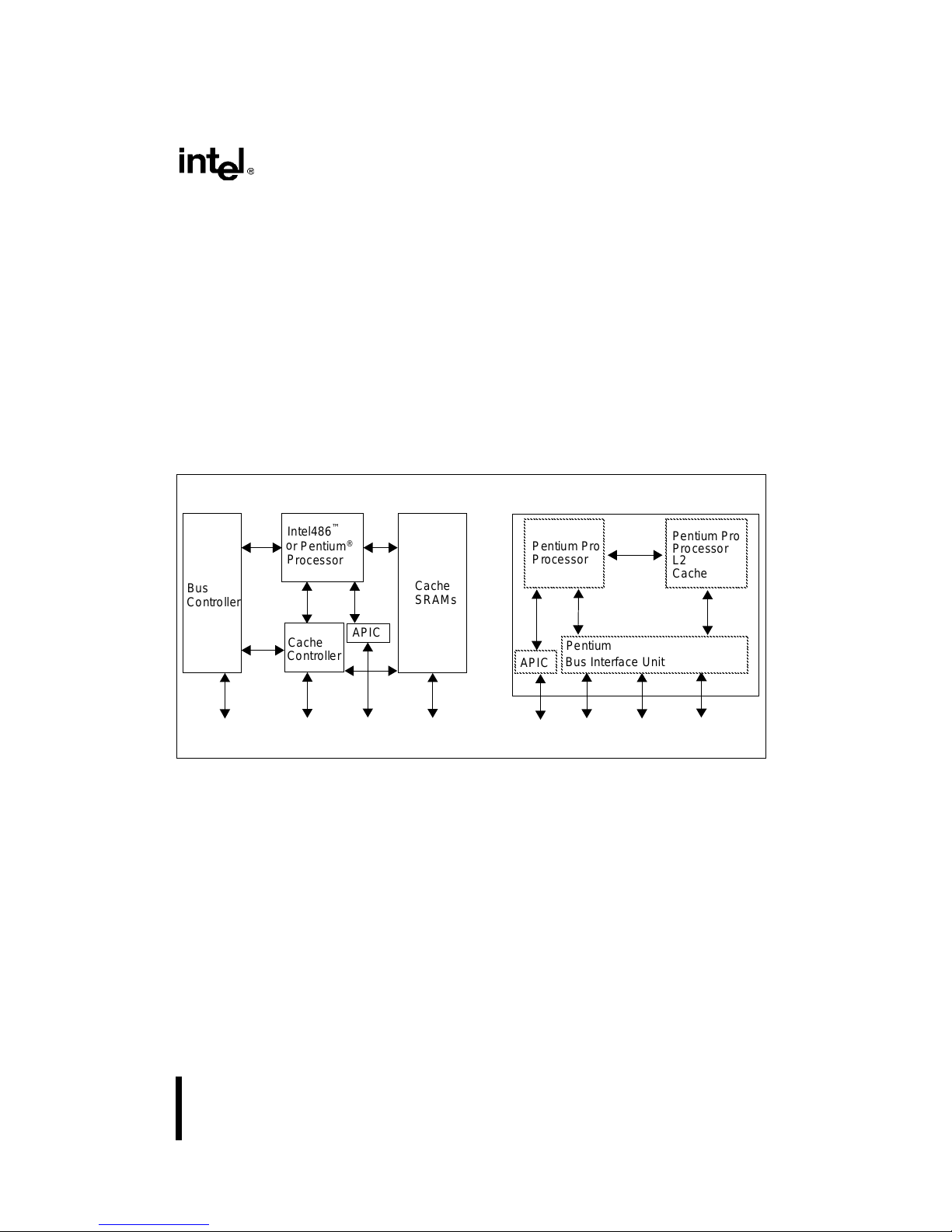
CHAPTER 1
AAAA
AAAA
AAAA
AAAA
AAAA
AAAA
AAAA
AAAA
AAAA
AAAA
AAAA
AAAA
AAAA
AAAA
COMPONENT INTRODUCTION
The Pentium® Pro microprocessor is the next generation in the Intel386™, Intel486™, and Pentium family of processors. The Pentium Pro processor implements a Dynamic Execution microarchitecture — a unique combination of multiple branch prediction, data flow analysis, and
speculative execution while maintaining binary compatibility with the 8086/88, 80286,
Intel386, Intel486, and Pe ntium processors. The Pentium Pro processor inte grates the second
level cache, the APIC, and the memory bus controller found in previous Intel processor families
into a single component, as shown in Figure 1-1.
™
I
n
t
8
6
4
l
Bus
Controll e r
e
o
r
P
r
®
t
P
e
n
u
m
i
o
s
c
e
o
r
s
Pentium Pro
Processor
Cache
SRAMs
Pentium P ro
Processo r
L2
Cache
Cache
Controller
APIC
Pentium Pro Processor
Bus Interface Uni t
APIC
Figure 1-1. The Pentium® Pro Processor Integrating the CPU, L2 Cache, APIC and Bus
Controller
A significant new feature of the Pentium Pro processor, from a system perspective, is the builtin direct multi-processing support. In order to achieve multi-processing for up to four processors
and maintain the memory and I/O bandwidth to support them, new system designs are needed
which consider the a dditional power require ments and signal integrity iss ues of supporting up
to eight loads on a high speed bus.
®
The Pentium Pro processor may be upgraded by a future OverDrive
processor and matching
voltage regulator module described in Chapter 17, OverDrive® Processor Socket Specification.
Since increasing clock frequencies and silicon density can complicate system de signs, the Pen-
tium Pro processor integrates several syste m components whic h allevi ate some of the previ o us
system requirem ents. The second le vel cache, ca che controller, and Advanced Program mable
Interrupt Controller (APIC) are some of the components that existed in previous Intel processor
1-1
Page 19

COMPONENT INTRODUCTION
family systems whi ch are inte grated int o this single com ponent. This integra tion result s in the
Pentium Pro processor bus m ore close l y resembl ing a symm etric m ulti-processing (SM P ) system bus rather than a previous generation processor-to-cache bus. This added level of integration
and improved performance results in higher power consumption and a new bus technology . This
means it is more important than ever to ensure adherence to the specifications contained in this
document.
1.1. BUS FEATURES
The desig n of the exte rnal Penti um Pro processor b us enables it to be “mul tiprocessor ready.”
Bus arbitration and control, cache coherency circuitry , an MP interrupt controller and other system-level f unctio ns are integrat ed into the b us interfa ce.
To relax timi ng const rai nts, the Penti um Pro proce ssor imple me nts a synch ronous, latched b us
protocol to enable a full clock cycle for signal transmissi on and a full clock cycle for signal interpretation and generation. This latche d pr otocol simplifies interco nnect timing re quirement s
and supports higher frequency system designs using inexpensive ASIC interconnect technology.
The Pentium Pro processor bus uses low-voltage-swing GTL+ I/O buffers, making
high-frequency signal communication easier.
All output pins are actually implemented in the Pentium Pro processor as I/O buffers. This buffer
design complies with IEE E 1149.1 Boundary Scan Specification, allowing all pins to be sa mpled and tested. An output only buffer is used only for TDO, which is not sampled in the boundary scan chain. A pin is an output pin when it is not an input for normal operation or FRC.
Most of the Pentium Pro process or cache protocol complexit y is handled by the processor. A
non-caching I/O bridge on the Pentium Pro processor bus does not need to recognize the cache
protocol and does not need snoop logic. The I/O bridge can issue standard memory accesses on
the Pentium Pro processor bus, which a re transparently sn ooped by all Pentium Pro processor
bus agents. If data is modified in a Pentium Pro processor cache, the processor transparently provides data on the bus, instead of the memory controller. This functionality eliminates the need
for a back-off capability that existing I/O bridges require to enable cache writeback cycles. The
memory controller must observe snoop response signals driven by the Pentium Pro processor
bus agents, absorb writeback data on a modified hit, and merge any write data.
The Pentium Pro processor inte grat es mem or y type range registe rs (MTRR s) to replac e the external address decode logi c used to decode cachea bil ity attribute s.
The Pentium Pro p rocessor bus protocol enabl es a near linea r increas e in system per formance
with an increase in the number of proce ssors. T he Pentium Pr o processor interfaces to a multiprocessor system without any support logic. This “glueless” interface enables a desktop system
to be built with an upgrade socket for another Pentium Pro processor.
The external Pentium Pro processor bus and Pentium Pro processor use a ratio clock design that
provides modularity and an upgrade path. The processor internal clock frequency is an n/2 multiple of the bus clock frequency where n is an integer equal to or greater than 4 but only certain
bus and processor frequency combinations are supported. Additional combinations are reserved
by this spec ification to provide future upgrade paths. See Section 9.2., “Clock Frequencies and
Ratios” for the bus and processor frequencies and combinations.
1-2
Page 20

COMPONENT INTRODUCTION
The ratio clock approach reduces the tight coupling between the processor clock and the external
bus clock. For a fixed system bus clock frequency, Pentium Pro processors introduced later with
higher processor clock frequencies can use the same support chip-set at the same bus frequency.
An investment in a Pentium Pro processor chip-set is protected for a longer time and for a greater
range of processor freq uencies. The ratio c loc k ap proach a lso pres erves system m o dularity, allowing the system electri cal topology to determine t he system bus clock freque ncy while process technology can determine the processor clock frequency.
The Pentium Pro processor bus archi tectu re provides a number of features t o support high reliability and high availability designs. Most of these additional features can be disabled, if necessary. Fo r exa mple, the b us arc hit ecture allows the data bus to be unprotected or protected with
an error correcting code (ECC). Error detection and limited recovery are built into the bus
protocol.
A Pentium Pro processor bus can contain up to four Pentium Pro processors, and a combination
of four other loads consisting pri marily of bus cluste rs, memo ry controllers, I/O bridges, an d
custom attachments.
In a four-processor system, the data bus is the most critical resource. To account for this situation, the Pentium Pro processor bus implements several features to maximize available bus
bandwidth including pipelined transactions in which bus transactions in different phases overlap, an increase in transaction pipeline depth over previous generati ons, and support for deferring a transaction for later completion .
The Pentium Pro processor bus architecture is therefore adaptable to various classes of systems.
In desktop multiprocess or systems, a subset of the bus features can be used. In server designs,
the Pentium Pro processor bus provides an entry into low-end multiprocessi ng offering linear
increases in performance as CPUs are added to scale performance upward allowing Pentium Pro
proces sor s ys tem s to be s uperi or for app lic ati ons tha t would otherwise in di cat e a do wnsi ze d
solution.
1.2. BUS DESCRIPTION
The Pentiu m Pr o proce ssor bus is a de mu ltiplex ed bu s with a 64-bi t data p ath an d a 36-b it
address path. This section provides more details on the bus features introduced in the preceding
section:
Ease of system desi gn
•
Efficient bus utilization
•
Multiproces sor ready
•
Data integrity
•
1-3
Page 21

COMPONENT INTRODUCTION
1.2.1. System Design Aspects
The P entiu m Pro processor bus clock and the Pentium Pro processor internal execution clock
run at different frequencies, related by a ratio. Section 9.2., “Clock Frequencies and Ratios” provides more information about bus frequency and processor frequency.
The Pentium Pro processor bus use s GTL+ . The GTL+ low volt age swi ng red uces both power
consumption and electromagnetic interference (EMI). The low voltage swing GTL+ I/O buffers
also enable direct drive by A SICs and ma ke hig h-frequency s ignal c omm unication easier and
cheaper to imple ment .
The Pentium Pro processor bus is a synchronous, latched bus. The bus protocol latches all inputs
on the bus clock rising edge, which are used internally i n the following cycle. The Pentium Pro
processor and other bus agents drive outputs on the bus clock rising edge. The bus protocol
therefore provides a full cycle for signal transmi ssi o n and an agent also has a full cloc k period
to determine its out p ut.
1.2.2. Efficient Bus Utilization
The Pentium Pro processor bus supports multiple outstanding bus transactions. The transaction
pipeline depth is limited to the smallest depth supported by any agent (processors, memory, or
I/O). The Pentium P r o proce ssor bus can be configured at power-on to support a maximum of
eight outstanding bus transactions depending on the amount of buffering available in the system.
Each Pentium Pro processor is capable of issuing up to four outstanding transactions.
The Pentium Pro processor bus enables transactions with long latencies to be completed at a later time using separate deferred reply transactions. The same Pentium Pro processor bus agent or
other Penti um Pro processor bus agents can co ntinue with s ubsequent reads an d writes while a
slow agent is processing an outstanding request.
1.2.3. Multiprocessor Ready
The Pentium Pr o processor bus enables multiple Pentium Pro processors to operate on one bus,
with no external support logic. The Pentium Pro processor requires no separate snoop generation
logic. The processor I/O buffers can drive the Pentium Pro processor bus in an MP system.
The Pentium Pro process ors and bus support a MESI cache protocol in the inter nal caches. The
cache protocol enables direct cache-to-cache line transfers with memory reflection.
The Pentium Pro processors and b us support fair, symme tric, round-robin bus arbitration that
minimizes overhead associated with bus ownership exchange. An I/O agent may generate a high
priority bus request.
1-4
Page 22
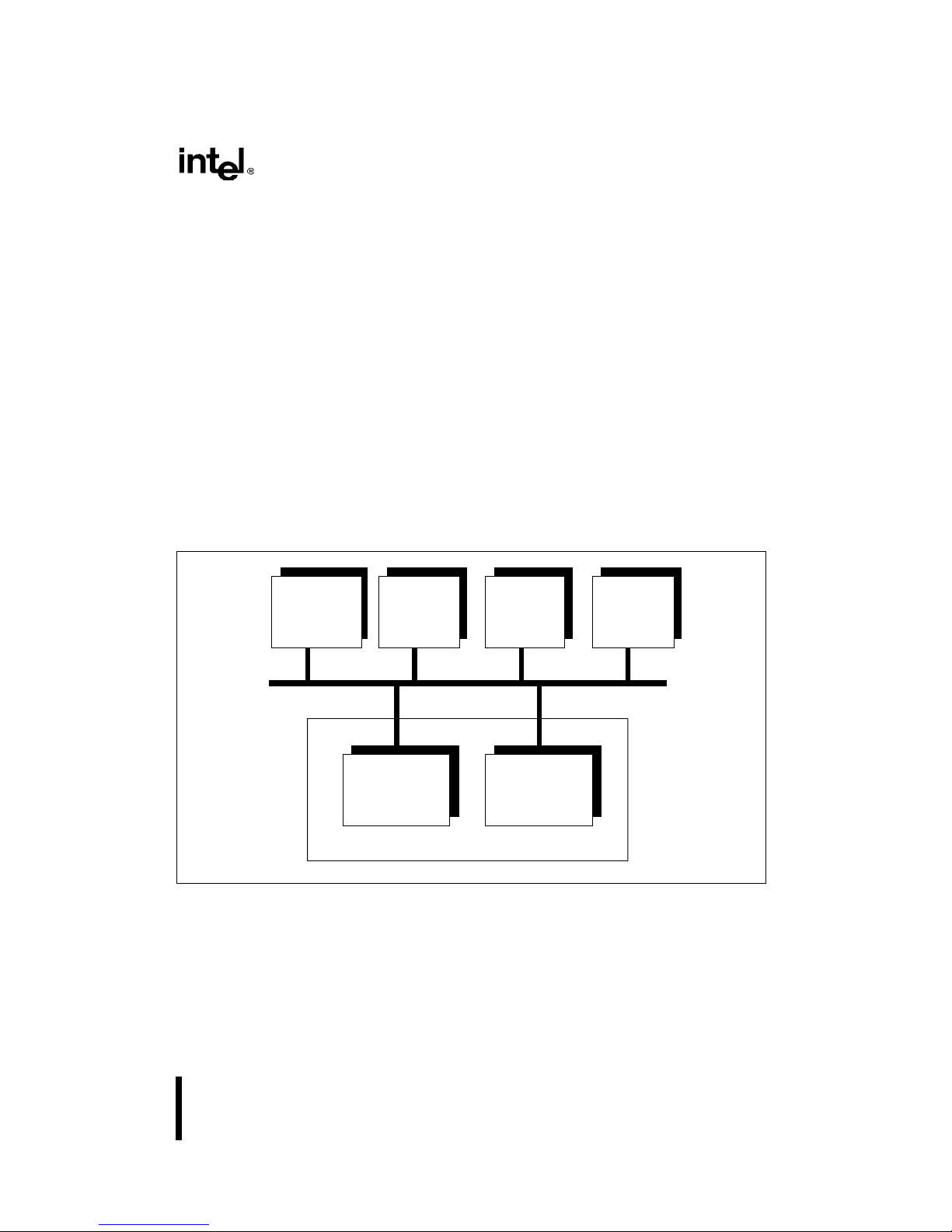
COMPONENT INTRODUCTION
1.2.4. Data Integrity
The Pentium Pro proce ssor bus provides parity si gnals for address, re quest, and response signals. The bus protocol supports retrying bus requests.
The Pentium Pro processor bus supports error correcting code (ECC) on the data bus and has
correction capability at the receiver.
The Pentium Pro processor supports functional redundancy checking (FRC ), similar to that of
the Pentium processor. FRC support e na bles the Pentium Pro processor to be used in hi gh dataintegrity, fault-tolerant applications. In addition, two Pentium Pro processors can be configured
at power-on as an FRC pair or a multiprocessor-ready pair.
1.3. SYSTEM OVERVIEW
Figure 1-2 illustrates t he Pent ium Pro proc essor system environm ent, conta ining multiple processors (MP), memory, and I/O. This particular archit ec tura l view is not intended t o imply an y
implementation trade-offs.
Pentium® Pro
Processor Processor
P6
Agent 0
Pentium Pro
Agent 1
High Speed I/O
Interface
System Interface
Pent ium Pro
Processor Processor
Agent 2
Memory
Interface
Pentium Pro
Agent 3
Figure 1-2. Pentium® Pro Processor System Interface Block Diagram
1-5
Page 23

COMPONENT INTRODUCTION
Up to four Pentium Pro processors can be gluelessly interconnected on the Pentium Pro processor bus. These agents are b us masters, capable of supporting all the features des cribed in this
document. The interface to the remainder of the system is represented by the high-speed I/O interface and memory interface bl ocks. The memory inte rface bloc k represents a path to system
memory capable of supporting over 500 Mbytes/second data bandwidth. The high-speed I/O interface block provides a fast path to system I/ O. Various impleme ntations of the se two block s
can provide different cost vs. performance t rade-offs. F or exam ple , more tha n one me mory interface or high-speed I/O interface may be included.
An MP system containing more than four Pentium Pro processors can be created based on clusters that each contai n four processors. Such a system can use cluster controllers that connect
Pentium Pro processor buses to a global memory bus. The Pentium Pro processor bus provides
appropriate protocol support for building external caches and memory directory-based systems.
1.4. TE R MINOLOGY CLARIFICATION
Some key definitions and concepts are introduced here to aid the unde rstanding of this
document.
A ‘#” sym bol a fte r a si gnal na me refers to an ac tive low signa l. Thi s means that a si gnal i s in
the active state (based on the name of th e s ignal) when d riven low. For example, when FLUSH#
is low a flush has been requested. When NMI is high, a Non-maskable interrupt has occ urred.
In the case of lines where the name does not imply an active state but describes part of a binary
sequence ( such as address or da ta), t he ‘#’ sym bol im plies th at th e signal is invert ed. For
example, D[3:0] = ‘HLHL’ refers to a hex ‘A’, and D#[3:0] = ‘LHLH’ also refers to a hex
‘A’. (H= High logic level, L= Low logic level )
Pentium Pro processor bus agent s issue t ransactions to transfer data an d system information.
A bus agent is any device that connects to the processor bus inclu ding the Pentium Pro proce ssors themselves.
This specification refers to several classificat ions of bus agents.
Central Ag ent. Handles reset, hardware configuration and initializa tion, spec ial transa c-
•
tions, and centralized hardware error detecti on and handlin g.
I/O Agent. Interfaces to I/O devices using I/O port addresses. Can be a bus bridge to
•
another bus used for I/O devices, such as a PCI bridge.
Memory Agent. Provi des access to main memory.
•
A particular bus agent can have one or more of several roles in a transaction.
Requesting Agent. The agent that issues the transac tio n.
•
Addressed Agent. The agent that is addressed by the transac tion. Al so called the Target
•
Agent. A memory or I/O transaction is addressed to the memory or I/O agent that
recognizes the specified memory or I/O address. A Deferred Reply transaction is addressed
to the agent tha t issued the original transa ction. Special transa ctions are conside red to be
issued to the central agent.
1-6
Page 24

COMPONENT INTRODUCTION
Snooping Agent. A caching bus agent that observes (“snoops”) bus transactions to
•
maintain ca che coheren cy.
Responding Agent. The agent that provides the res ponse on the RS[2:0]# signals to the
•
transaction. Typically the addressed agent.
Each transaction has several phases that include some or all of the following phases.
Arbitration Phase. No transactions can be issued until the bus agent owns the bus. A
•
transaction onl y needs to have this phase if the agent that wants to drive the tra nsaction
doesn’t already own the bus. Note that there is a distinction between a symmetric bus
owner and the actual bus owner. The actual bus owner is the one and only bus agent that is
allowed to drive a transaction at that time. The symmetric bus owner is the bus owner
unless the priority agent owns the bus.
Request Phase. This is the phase in which the transaction is actually issued to the bus. The
•
request agent drives ADS# and the address in this phase. All transactio ns must have this
phase.
Error Phase . Any errors that occur during the Request Phase are reported in the Error
•
Phase. All transactions have this phase (1 clock).
Snoop Phase. This is the phase in which ca che coherency is enforced. All caching agents
•
(snoop agents) drive HIT# and HITM# to appropriate values in this pha se. All memory
transactions have this phase.
Response Phase. The response agent drives the transaction response during this phas e.
•
The response agent is the target device addressed during the Request Phase unless a
transaction is deferred for later completion. All transactions have this phase.
Data Phase. The re sponse agent drive s or accepts the transac tio n data, if t here is a ny. Not
•
all transactions have this phase.
Other commonly used terms include:
A request initiated data transfer m ea ns that the re quest agent has writ e data to tra ns fe r. A re -
quest initia te d da t a t ra nsfer ha s a request initiated TRDY# assertion.
A response initiated data transfer means that the response agent must provide the rea d data to
the request agent.
A snoop initiated data transfer means that there was a hit to a modified line during the snoop
phase, and the agent that assert ed HITM # is going to drive the modified data to the bus. This is
also called an implicit writeback because every time HITM# is asserted, the addressed memory
agent knows that writeback data will follow. A snoop init iated data transfer has a snoop initiated
TRDY# assertion .
There is a DEFER# signal that is sampled during the Snoop Phase to determine if a transaction
can be guaranteed in-order completion at tha t time. If the DEFE R# si g nal is asserted, only t w o
responses are allowed by the bus protocol during the Response Phase, the Deferre d Response
or the Retry Response . If the Deferred Response is given, the response agent must later complete
the transactio n with a Deferred Reply transaction.
1-7
Page 25

COMPONENT INTRODUCTION
1.5. COMPATIBILITY NOTE
In this document, some regis ter bits are Intel Reserved. When reserve d bits are documented,
treat them as fully undefined. This is essential for software compatibility with future processors.
Follow the guidelines below:
1. Do not depend on the states of any undefined bits when testing the values of defined
register bits. Mask them out whe n testing.
2. Do not depend on the states of any undefined bits when storing them to memory or another
register.
3. Do not depend on the abi lity to retain informa tio n written into an y undefined bits.
4. When loading registers, always load the undefined bits as zeros.
1-8
Page 26

Pentium® Pro
Processor
Architecture
Overview
2
Page 27

Page 28

CHAPTER 2
®
PENTIUM
PRO PROCESSOR
ARCHITECTURE OVERVIEW
The Pentium Pro processor has a decoupled, 12 -stage, superpipel ined impleme ntatio n, trading
less work per pipestage for more stages . The Pentium Pro p rocessor also has a pipe stage time
33 percent less than the Pentium processor, which helps achieve a higer clock rate on any given
process.
The approach used by the Pentium Pro processor removes the constraint of linear instruction sequencing between the traditional “fetch” and “execute” phases, and opens up a wide instruction
window using an instruction pool. This approach allows the “execute” phase of the Pentium Pro
processor to have much more visibility into the program’s instruction stream so that better
scheduling may t ake pl ac e. It re q uires the instruction “fetch/decode” phase of the Pent ium Pro
processor to be much more intelligent in terms of predicting program flow. Optimized scheduling requires the fundamental “exec ute” phase to be replace d by decoupled “dispat ch/execut e”
and “retire” phases. This allows instructions to be started in any order but always be completed
in the original program order. The Pentium Pr o processor is implement ed a s three independent
engines coupled with an instruction pool as shown in Figure 2-1.
.
Fetch/
Decode
Dispatch
/Execute
Retire
Unit
Unit
Unit
Instruction
Pool
Figure 2-1. Three Engines Communicating Using an Instruction Pool
2-1
Page 29

PENTIUM® PRO PROCESSOR ARCHITECTURE OVERVIEW
2.1. FULL CORE UTILIZATION
The three independent-engine approach was taken to more fully utilize the CPU core. Consider
the code fragment in Figure 2-2:
r1 <= mem [r0] /* Instruction 1 */
r2 <= r1 + r2 /* Instruction 2 */
r5 <= r5 + 1 /* Instruction 3 */
r6 <= r6 - r3 /* Instruction 4 */
Figure 2-2. A Typical Code Fragment
The first instruct ion in this example is a load of r1 that, at run time, causes a cache mis s. A traditional CPU core must wait for its bus interface unit to read this data from main memo ry and
return it before moving on to instruction 2. This CPU stalls while waiting for this data and is thus
being under-utili zed .
T o avoid this memory latency problem, the Pentium Pro processor “looks-ahead” into its instruction pool at subsequent instructions and will do useful work rather than be stalled. In the example in Figure 2-2, instructi on 2 is not e xecutable since it depends upon the result of instruction
1; however both instruc tions 3 and 4 are execut able. The P entium Pro processor exe cutes instructions 3 and 4 out-of-order. The results of this out-of-order execution can not be comm it ted
to permanent machine sta te (i.e ., the p rogra mme r-visi ble registers) immedia te ly since the original program order must be mai ntained. The result s are instea d stored back in t he instruct ion
pool awaiting in-order retirement. The core executes instructions depending upon their readiness
to execute, and not on their original program order , and is therefor e a true da taflow engine. Th is
approach has the side effect that instructions are typically executed out-of-order.
The cache miss on instruction 1 wi ll take many internal clocks, so the Pentium Pro processor
core continues to l o ok ahea d for ot her ins truct ions that co uld be s pecul at ive ly exec uted, and i s
typically looking 20 to 30 instructions in front of the instruct ion pointer. Within this 20 to 30
instruction window there will be, on average, five branches that the fetch/decode unit must correctly predict if the dispatch/execute unit is to do useful work. The sparse register set of an Intel
Architecture (IA) processor will create many false dependencies on registers so the dispatch/execute unit wi ll rename the IA re gisters into a la rger register set to enabl e additional forward
progress. T he retire unit owns the programmer’s IA register set and results are only committ ed
to permanent machi ne state in these regis ters when it remove s completed i nstruct i ons from the
pool in original program order .
Dynamic Execution technology can be summarized as optimally adjusting instruction execution
by predicting program flow, having the ability to speculatively execute instructions in any
order, and then analyzing the pro gram’s dataflow graph to ch oose the best order to ex ec ute
the instr ucti ons.
2-2
Page 30
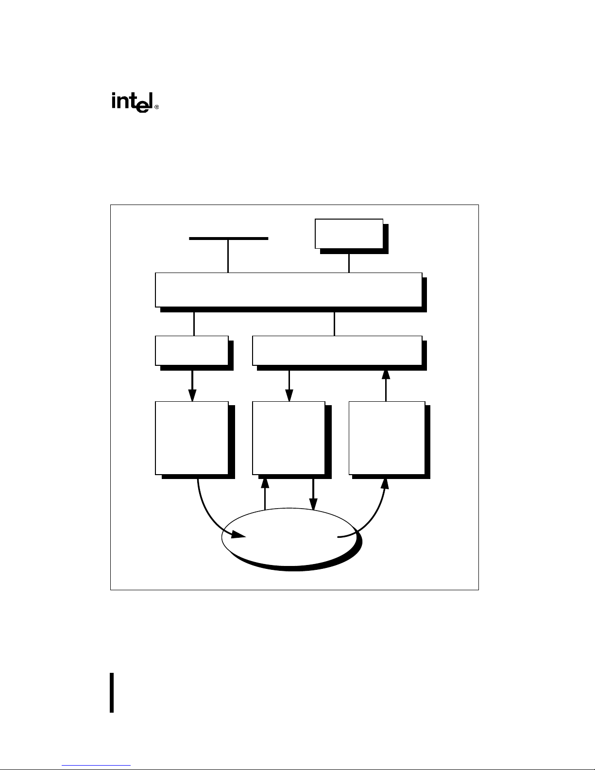
PENTIUM® PRO PROCESSOR ARCHITECTURE OVERVIEW
2.2. THE PENTIUM® PRO PROCESSOR PIPELINE
In order to get a closer look at how the Pentium Pro processor implements Dynamic Execution,
Figure 2-3 shows a block diagram including cache and memory interfaces. The “Units” shown
in Figure 2-3 represent stages of the Pentium Pro process or pipel ine .
System Bus
L2 Cache
Bus Interface Unit
L1 ICache L1 DCache
Fetch Load Store
Fetch/
Decode
Unit
Dispatch
/Execute
Unit
Retire
Unit
Figure 2-3. The Three Core Engines Interface with Memory via Unified Caches
Instruction
Pool
2-3
Page 31

PENTIUM® PRO PROCESSOR ARCHITECTURE OVERVIEW
The FETCH/DECODE unit: An in-order unit that takes as input the user program
•
instruction stream from the instruction cache, and decodes them into a series of microoperations (µops) that represent the dataflow of that instructio n strea m. The pre-fetch is
speculative.
The DISPATCH/EXECUTE unit : An out-of-order unit that accepts the dataflow stre am,
•
schedules executi on of the µ ops subj ect to data depe n dencies and res ourc e availabi li ty and
temporarily stores the results of these spec ula tive exec utio ns.
The RETIRE unit : An in-order unit that kn ows how and when to commit (“retire”) the
•
temporary, speculative results to perma nent arc hit ectural state .
The BUS INTERFACE unit: A partially ordered unit responsible for connecting the three
•
internal units to the real world. The bus interface unit communicates directly with the L2
(second level ) cache supporting up to four concurrent cache accesses. The bus interface
unit also controls a transaction bus, with MESI snooping protocol, to system memory.
2.2.1. The Fetch/Decode Unit
Figure 2-4 shows a more detailed view of the Fetch/Decode Unit.
From BIU
2-4
ICache
ID
(x3)
Next_IP
BTB
BIU - Bus Interface Unit
ID - Instruction Decoder
BTB - Branch Target Buffer
MIS - Microcode Instruction
Sequenc er
RAT - Register Alias Table
ROB - ReOrder Buffer
MIS
RAT
Allocate
Figure 2-4. Inside the Fetch/Decode Unit
To
Instruction
Pool (ROB)
Page 32

PENTIUM® PRO PROCESSOR ARCHITECTURE OVERVIEW
The ICache is a l ocal ins truct ion cac he. The N ext_IP uni t provides the ICa che inde x, based o n
inputs from the Branch Target Buffer (BTB), trap/interrupt status, and branch-misprediction indications from the integer execution section.
The ICache fetches the cache line corresponding to the index from the Next_IP, and the next line,
and presents 16 aligned bytes to the decoder. The prefetched bytes are rota ted so that they are
justified for the instructio n decoders (ID). The beginning and end of the IA instructions are
marked.
Three parallel decoders a ccept this stream of marked bytes, and proceed to find and decode the
IA instructions contained therein. The decoder converts the IA instructions into triadic µops (two
logical sources, one logical destination per µop). Most IA instructions are converted directly into
single µops, some instructions a re decode d into one-t o-four µops an d the comple x instruc tions
require microcode (t he box labeled MIS in Figure 2-4). T his microcode is j ust a se t o f preprogrammed sequences of normal µops. The µops are queued, and sent to the Regi ster Alias Table
(RAT) unit, where the logical IA-based register refere nces are converted int o Pentium Pro processor physical register references, and to the Allocator stage, which adds status information to
the µops and enters them into the inst ruction pool. The inst ruction pool is implem ented as an
array of Content Addressable Memory called the ReOrder Buffer (ROB).
This is the end of the in-order pipe.
2.2.2. The Dispatch/Execute Unit
The dispatch unit selects µops from the instruction pool depending upon th eir st atus. If the status
indicates that a µop ha s all of i ts o perands then the dispa tch u nit che cks to se e if the exec utio n
resource needed by that µo p is also available . If b oth are true, the R eservat ion Station removes
that µop and sends it to the resource where it is executed. The results of the µop are later returned
to the pool. There are five ports on the Reservation Station, and the multiple resources are
accessed as shown in Figure 2-5.
2-5
Page 33

PENTIUM® PRO PROCESSOR ARCHITECTURE OVERVIEW
RS - Reservation Station
EU - Execution Unit
FEU - Floating Point EU
IEU - Integer E U
JEU - Jum p E U
AGU - Address Generation Unit
ROB - ReOrder Buffer
To/from
Instruction
RS
Port 0
Port 1
FEU
IEU
JEU
IEU
Pool (RO B )
Port 2
Port 3,4
Figure 2-5. Inside the Dispatch/Execute Unit
The Pentium Pro processor can schedule at a peak rate of 5 µops per clock, one to each resource
port, but a sustained rate of 3 µops per clock is typical. The activity of this scheduling process is
the out-of-order process; µops are dispatched to the execution resources strictly according to
dataflow constraints and resource availability, without regard to the original ordering of the
program.
Note that the actual algorithm employed by this execut ion-sc heduli ng process is vitally important to performance. If only one µop per resource becomes data-ready per clock cycle, then there
is no choice. But if several are available, it must choose. The Pentium Pro processor uses a pseudo FIFO scheduling algorithm favoring back-to-back µops.
AGU
AGU
Load
Store
Note that many of the µ ops are br a nches. The Branc h Target Buffer will correctly predict most
of these branches but it can’t correctly predict them all. Consider a BT B that is correctly predicting the backward branch at the bottom of a loop; eventually that loop is going to terminate, and
when it does, that branch will be mispredicted. Branch µops are tagged (in the in-order pipeline)
with their f all- throu gh address and the destination that was predicted for them. When the branch
executes, what the branch actually did is compared against what the prediction hardware said it
would do. If those coincide, then the branch eventually retires, and most of the speculatively executed work behind it in the instruction pool is good.
But if they do not coincide, then the Jump Execution Unit (JEU) changes the status of all of the
µops behind the branch to remove them from the instruction pool. In that case the proper branch
destination is provided to the BTB which restarts the whole pipeline from the new target address.
2-6
Page 34

PENTIUM® PRO PROCESSOR ARCHITECTURE OVERVIEW
2.2.3. The Retire Unit
Figure 2-6 shows a more detailed view of the Retire Unit.
To/from DCache
R
MIU
S
RS - Reservation Station
MIU - Memory Interface Unit
RRF - Retirement Register File
RRF
From To
Instruction Pool
Figure 2-6. Inside the Retire Unit
The retire unit is a lso che cking t he status of µo ps in the instruct i on pool. It is lo oking for µ ops
that have executed and can be removed from the pool. Once removed, the original architectural
target of the µops is written as per the original IA instruction. The retirement unit must not only
notice which µops are complete, it must also re-impose the origina l program order on them. It
must also do this in the face of interrupts, traps, faults, breakpoints and mispredictions.
The retirement unit must first read the instruction pool to find the potential candidates for retirement and determine whic h of these candidates are ne xt in the original program order. Then it
writes the results of this cycle’s retirements to both the Instruction Pool and the Retirement Register File (RRF). The retirement unit is capable of retiring 3 µops per clock.
2.2.4. The Bus Interface Unit
Figure 2-7 shows a more detailed view of the Bus Interface Unit .
2-7
Page 35

PENTIUM® PRO PROCESSOR ARCHITECTURE OVERVIEW
MOB - Memory Order Buffer
Sys Mem
MOB
Mem
L2 Cache
There are two types of memory access: loads and stores. Loads only need to specify the memory
address to be accessed, the width of the data being retrieved, and the destination register. Loads
are encoded into a single µop.
Stores need to provide a memory address, a data width, and the data to be written. Stores therefore require two µops, one to generate the address, and one to generate the data. These µops must
later re-combine for the store to complete.
Stores are never performed speculatively since there is no transparent way to undo them. Stores
are also never re-ordered among themselves. A store is dis patched only when b oth the address
and the data are available and there are no older stores awaiting dispat c h.
I/F
Figure 2-7. Inside the Bus Interface Unit
DCache
From
AGU
AGU - Address Generation Unit
ROB - ReOrder Buffer
To/from
Instruction
Pool (ROB)
A study of the importance of memory access reordering concluded:
Stores must be constrained from passing other stores, for only a small impact on
•
performance.
Stores can be constrained f rom passing loads, for an inconsequent ia l performance loss.
•
Constraining loads from passing other loads or stores has a significant impact on
•
performance.
The Memory Order Buffer (MOB) allows l oads to pass other loads and stores by actin g like a
reservation station and re-order b uffer. It holds suspended loads and stores and re-dispatche s
them when a blocking condition (dependency or resource) disappears.
2.3. ARCHITECTURE SUMMARY
Dynamic Ex ecu ti on i s t hi s co mb in ation of im p rov ed bran ch p r ed ict io n , sp ecu l ati ve ex ec ution and data flow ana lysis that enables the Pentium Pr o processor to deliver i ts superior
performance.
2-8
Page 36

Bus Overview
3
Page 37

CHAPTER 3
BUS OVERVIEW
This chapter provides an overview of the Pentium Pro processor bus protocol, transactions, and
bus signals. The Pentium Pro processor supports two other synchronous busses, APIC and
JTAG. It also has PC compat ibility signals and implementa tion specific signals. This chapte r
provides a functional description of the Pentium Pro processor bus only. For the Penti um Pro
processor bus protocol specifications, see Chapter 4, Bus Protocol. For details on the Pent ium
Pro processor bus transactions, see Chapter 5, Bus Transactions and Operations. For the full
Pentium Pro processor signal specifications, see Appendix A, Signals Refer ence and Table 11-2.
3.1. SIGNAL AND DIAGRAM CONVENTIONS
Signal names use uppercase letters, such as ADS#. Signal s in a set of related signals are disti nguished by numeric suffixes, such as AP1 for address parity bit 1. A set of sig nals covering a
range of numeric suffixes is denoted as AP[1:0], for address parity bits 1 and 0. A # suffix indicates that the signal is active low. A signal name without a # suffix indicates that the signal is
active high.
In many cases, signals are mapped one -to-one to physical pins with the same names. In other
cases, different signals are mapped onto the same pin. For example, this is the case with the address pins A[35:3]#. During the first clock of the Request Phase, the address signals are driven.
The first clock is indicated by the lower case a, or just the pin name itself: Aa[35:3]#, or
A[35:3]#. During the second clock of the R equest Phase other i nf ormation is driven on the re quest pins. These signals are referenced either by their functional signal names DID[7:0]#, or by
using a lower c ase b wi t h the pin name: A b [23:16]#. Note also that severa l pins h a ve c o n figu ration functions at the active to inactive edge of RESET#.
The term asser ted implies tha t a signal is driven to its active level (logic 1, FR CERR hig h, or
ADS# low). The term deasserted implies tha t a signal is driven to its inactive level (logic 0,
FRCERR low, or ADS# high). A signal driven to its active level is said to be active; a signal
driven to its inactive level is said to be inactive.
In timing diagram s, sq uare an d circl e s ym b ols indic ate the c loc k in w hi ch pa rti cula r sig nals of
interest are dri ven and sampl ed. The s quare in dicates that a signal is drive n in that c lock. The
circle indicates that a signal is sampled in that clock.
All timing diagrams in this specifi catio n show signals as they are driven ass erted or dea sse rted
on the Penti um P ro p rocess or bus. There is a one -clock de lay in the signal values observe d b y
bus agents. Any signal names that appear in lower case letters in brackets {rcnt} are internal signals only, and are not driven to the bus. Upper case letters that appear in brackets represe nt a
group of signals such as the Request Phase signal s {REQUEST }. The timing diagrams sometimes include internal signals to indicate internal states and show how it affects external signals.
3-1
Page 38

BUS OVERVIEW
When signal values are referenced in tables, a 0 indicates inactive and a 1 indicates active. 0 and
1 do not reflect voltage levels. Remember, a # after a signal name indicates active low. An entry
of 1 for ADS# means that ADS# is active, with a low voltage level.
3.2. SIGNALING ON THE PENTIUM® PRO PROCESSOR BUS
The Pentium Pro processo r bus supports a synchronous latched protocol. On the rising edge o f
the bus clock, all agents on the Pentium Pro processor bus are required to drive their active outputs and sample required inputs. No additional logic is loc ated in the output and input paths between the buffer and the latch sta ge, thus keeping setup and hold times constant for all bus
signals following the latched protocol. The Pentium Pro processor bus requires that every input
be sampled duri ng a va lid samp ling w i ndow on a r ising cl oc k edge an d it s effec t be driv en
out no sooner than the next rising clock edge. This approach allows one full clock for intercomponent communica tion and at least one full clock at the receiver to compute a response.
Figure 3-1 illustrates the latched bus protocol as it appears on the bus. In subseq uent descriptions, the protocol is de scribed as “B# is asserted i n the clock after A# i s observed ac tive”, or
“B# is asserted two clocks after A# is asserted”. Note that A# is asserted in T1, but not observed
active until T2. The receiving agent uses T2 to determine its response and asserts B# in T3. Other agents observe B# active in T4.
The square and circle symbol s are used in the timing diagrams to indica te the clock in which
particular signals of interest are driven and sampled. The square indicates that a signal is driven
(asserted, initiated) in that clock. The circle indicates that a signal is sampled (observed, latched)
in that clock.
3-2
Page 39

BUS OVERVIEW
Full cloc k allo w ed
for signal propagation
BCLK
12 34
A#
B#
Assert A#
Latch A#
Assert B#
Latch B#
Figure 3-1. Latched Bus Protocol
Full clock allowed
for logic delays
Any signal nam es that a ppe ar in bracke ts {} are inte rnal signa ls only, and are not driven t o the
bus. The timing diagrams sometimes include internal signals to indicate internal state and show
how it affects external signals. All timing diagrams in this specification show bus signals as they
are driven asse rte d or deasse rte d o n the Pe ntium Pro processor bus. I nterna l signa ls are shown
to change state in the clock tha t they would be driven to the bus if they were e xter nal signals.
Internal signals actually change state internally one clock earlier.
Signals that are driven in the sa me cloc k by mul tiple Penti um Pro process or bus agents exhibit
a “wired-OR glitch” on the elec trica l-low -to-el ec trica l-hi gh tra nsit i on. To account for this situation, these signal state transitions are specifie d to have tw o clocks of settling tim e when deasserted before they can be safely observed. The bus signals that must meet this crit eria are:
BINIT#, HIT#, HITM#, BNR#, AERR #, B ERR#.
3-3
Page 40

BUS OVERVIEW
3.3. PENTIUM® PRO PROCESSOR BUS PROTOCOL OVERVIEW
Bus activity is hierarchically organized into operations, transactions, and phases.
An operation is a bus procedure that appears atomic to software even though it may not be atom-
ic on the bus. An operation may consist of a single bus transaction, but sometimes may i nvolve
multiple bus transactions or a single transaction with multiple data transfers. Examples of complex bus operations include: locked read/modify/write operations and deferred operations.
A transaction is the set of bus a ctivities related to a single bus request. A transaction begins with
bus arbitration, and the assertio n of ADS# and a transact ion address. Transactions are driven to
transfer data, to inquire about or change cache state, or to provide the system with information.
A transaction contains up to six phases. A phase uses a specific set of signals to communicate a
particular type of information. The six phases of the Pentium Pro processor bus protocol are:
Arbitration
•
Request
•
Error
•
Snoop
•
Response
•
Data
•
Not all transactions contain all phases, and some phases can be overlapped.
3.3.1. Transaction Phase Description
Figure 3-2 s hows all of the Pentium Pro processor bus transa ction phases for two transact ions
with data transfers.
3-4
Page 41

BUS OVERVIEW
A
A
A
A
A
A
A
A
A
A
A
A
A
A
A
A
A
A
A
A
A
A
A
A
A
A
A
A
A
BCLK
Arbitration
Request
Error
Snoop
Response
Data Transfer
1 2 3
1
4
5
678
2
1
2
1
10 11 12*
9
2
1
2
13
AA
AA
AA
AA
AA
AA
AA
AA
AA
AA
AA
AA
AA
AA
AA
AA
AA
AA
AA
AA
AA
AA
AA
AA
AA
AA
AA
AA
AA
15
14
1
1
17
16
2
2
* NOTE: The shaded vertical bar indicates one or more clock cycles are allowed between different phases.
Figure 3-2. Pentium® Pro Processor Bus Transaction Phases
When the requesting agent does not own the bus, transactions begin with an Arbitratio n Phase,
in which a requesting agent becomes the bus owner.
After the requesting agent becomes the bus owner, the transaction enters the Request Phase . In
the Request Pha se, the bus ow ner drives re quest and ad dress information on the bus. The Request Phase is two clocks long. In the first clock, ADS# is driven along with the transaction address and sufficient information to begin snooping and memory access. In the second clock, the
byte enables, deferred ID, transaction length, and other transaction information are driven.
Every transaction’s third phase is an Error Phase which occurs three clocks after the Re quest
Phase begins. The Error Phase indicates any parity errors trig gered by the request.
Every transaction that isn’t cance lled because an error was indic ated in the Error Phase has a
Snoop Phase, four or more clocks from the Request Phase. The s noop results indicate if the address driven for a transaction references a valid or modified (dirty) cache line in any bus agent’s
cache. The snoop results also indicate whether a transactio n will be completed in-order or may
be deferred for possible out-of-order completion.
Every transaction that isn’t cance lled because an error was indic ated in the Error Phase has a
Response Phase. The Response Phase indicates whether the transaction has failed or succeeded,
whether transaction completion is immediate or deferred, whether the transaction will be retried,
and whether the transaction contains a Data Phase. The valid transaction responses are:
Normal Data
•
Implicit Writeback
•
No Data
•
Hard Failure
•
3-5
Page 42

BUS OVERVIEW
Deferred
•
Retry
•
If the transaction does not have a Data Phase, that transacti on is complete after the Re sponse
Phase. If the request agent has wri te data to transfer o r is requesting read data, the t ransaction
has a Data Phase which may extend beyond the Response Phase.
Not all transactions contain all phases, not all phases occur in order, and some phases can be
overlapped.
All transactions that are not cancelled in the Error Phase have the Request, Error, Snoop,
•
and Response Phases.
Arbitration can be e xplicit or implicit. The Arbitra tion Phase only needs to occu r if the
•
agent that is driving the next transactio n does not already own the bus.
The Data Phase only occurs if a transaction requires a data transfer. The Data Phase can be
•
absent, response initiated, req uest initiated, sn oop initiated, o r request and snoop initiated.
The Response Phase overlaps with the beginni n g of the Data Phase for read transacti on s.
•
The Response Phase (TRDY#) triggers the Data Phase for write transactions.
•
In addition, since the Pentium Pro processor bus supports bus transaction pipelining, phases
from one transaction can overlap phases from another transactio n, see Figure 3-2.
3.3.2. Bus Transaction Pipelining and Transaction Tracking
The Pentium Pro processor bus architecture supports pipelined transactions in which bus transactions in different phases overlap. The Pentium Pro processor bus may be configured to suppo rt
a maximum of 1 or 8 outstandi ng transactions simultaneously. Each Pent ium Pro processor is
capable of issuing up to four outstanding transactions.
In order to track transactions, all bus agent s must track certain transaction information. T he
transaction information that must be tracked by e ach bus agent is:
Number of transactions outstanding
•
What transaction is next to be snooped
•
What transaction is next to receive a response
•
If the transaction was issued to or from this agent
•
This information is tracked in a queue called an In-order Queue (IOQ). All bus agents maintain
identical In-order Queue status to track every transaction that is issued to the bus. When a transaction is issued to the bus, it is also entered in the IOQ of each agent. The depth of the smallest
IOQ is the limit of how many transactions can be outstanding on the bus simultaneously. Because transactions rec eive their responses and data in the same order as they were is sued, the
transaction at the top of the IOQ is the next transac tio n to enter the Response and Dat a Phases .
A transaction is removed from the IOQ after the Response Phase is complete or after an error is
detected in the Error Phase. The simplest bus agents can simply count events rather than implement a queue.
3-6
Page 43

BUS OVERVIEW
Other, agent specific, bus information must be tracked as well. Note that not every agent needs
to track all of this additio nal information. Examples of additio nal information that might be
tracked follow.
Request agents (agents that issue transactions) might track:
How many more transactions this agent can still issue?
•
Is this transaction a read or a write?
•
Does this bus agent need to provide or accept data?
•
Response agents (agents that can provide transaction response and data) might track:
Does this agent own the response for the transaction at the top of the IOQ?
•
Does this transaction contain an implicit writeback data and does this agent have to receive
•
the writeback data ?
If the transaction is a read, does this agent own the data transfer?
•
If the transacti on is a write, must this agent acc ept the data?
•
Availability of buffer resources so it can stall further transactions if it needs to.
•
Snooping agents (agents with a cache) mi ght track:
If the transaction needs to be snooped.
•
If the Snoop Phase needs to be extended.
•
Does this transaction contain an impli cit writeba ck data to be supplied by this agent?
•
How many snoop requests are in the queue.
•
Agents whose transactions can be deferred might track:
The deferred transactio n and its agent ID.
•
Availability of buffer resources.
•
This transaction information can be tracked by implementing multiple queues or one all encompassing In-order Queue. This document refers to these internal queue(s) as the Transaction
Queues (TQ), unless the In-order Queue is specifically being referenced. Note that the IOQ
is completely visible from the bus protocol, but the Transaction Queues use internal state
information.
3.3.3. Bus Transactions
The Pentium Pro processor bus supports the following types of bus transactions.
Read and write a cache line.
•
Read and write any combination of bytes in an aligned 8-byte span.
•
3-7
Page 44

BUS OVERVIEW
Read and write multiple 8-byte spans.
•
Read a cache line and invalidat e it in other caches.
•
Invalidate a cache line in other ca ches .
•
I/O read and write.
•
Interrupt Acknowledge (requiring a 1 byte interrupt vector).
•
Special transactions are use d to send va rious m es sages on t he bus. The spe cial transa ction
•
for the Pentium Pro processor are:
— Shutdown
— Flush
— Halt
— Sync
— Flush Acknowle d ge
— Stop Clock Acknowledge
— SMI Acknowledge
— Branch trace message (providing a n 8-byte branch trace address)
Deferred reply to an earlier read or write that received a deferred response.
•
Specific d escri ptions o f eac h transa ctio n can be f ound in Chap ter 5, B us Transactions and
Operations.
3.3.4. Data Transfers
The Pentium Pro process or bus distingui shes bet wee n mem ory and I/O transactions.
Memory transactions are used to transfer data to and from memory. Memory transact ions ad-
dress memory usin g the full width of the add ress bus. The Penti um Pro processor can a ddress
up to 64 Gbytes of physical memory.
I/O transactions are used to transfer data to and from the I/O address space. The Pentium Pro
processor limits I/O accesses to a 64K + 3 byte I/O address space. I/O transactions use A[16:3]#
to address I/O ports and a lways deassert A[35: 17]#. A16# is zero except when t he first three
bytes above the 64KByte address space are accessed (I/O wraparound). This is required for compatibility with previo us Intel pr ocess ors.
The Pentium Pro processor bus distinguishes betwee n different transfer lengths.
3-8
Page 45

BUS OVERVIEW
3.3.4.1. LINE TRANSFERS
A line transfer reads or writes a cache line, the uni t of caching in a Pentium Pro proces sor sys tem. On the Pentium Pro processor this is 32 bytes aligned on a 32-byte boundary. While a line
is always aligned on a 32-byte bo unda ry, a line transfer need not begin on that boundary. For a
line transfer on the Pentium Pro processor, A[35:3]# carry the upper 33 bits of a 36-bit physical
address. Address bits A[4:3]# determine the transfer order, called burst order. A line is trans -
ferred in four eight-byte chunks, each of which can be identified by address bits 4:3. The chunk
size is 64-bits. Table 3-1 specifies t he transfer order used for a 32-byte line, ba sed on address
bits A[4:3]# specified in the transact ion’s Request Phase.
Table 3-1. Burst Order Used For Pentium® Pro Processor Bus Line Transfers
A[4:3]#
(binary)
00 0 0 8 10 18
01 8 8 0 18 10
10 10 10 18 0 8
1 1 18 18 10 8 0
Requested
Address
(hex)
1st Address
Transferred
(hex)
2nd Address
Transferred
(hex)
3rd Address
Transferred
(hex)
4th Address
Transferred
(hex)
Note that the requested read data is always transferred first. Unlike the Pentium processor, which
always transfers w riteback dat a address 0 first, the Pentium Pro processor transfers wri teback
data requested address first.
3.3.4.2. PART LINE ALIGNED TRANSFERS
A part-line aligned transfer moves a quantity of data smaller than a cache line but an even multiple of the chunk size between a bus agent and memory using the burst order. A part-line transfer affects no more than one line in a cache.
A 16-byte transfer on a 64-bit data bus with a 32-byte ca che line size is a part-line transfer, where
a chunk is eight bytes aligned on an eight-byte boundary. All chunks in the span of a part-line
transfer are moved a cross the dat a bus. Address bi ts A[ 4:3]# determi nes the transfer o rder fo r
the included chunks, using the burst order specified in Table 3-1 for line transfers.
A 16-byte aligned transfer requires two dat a transfer cloc ks on a 64-bit bus. Not e that the Pe ntium Pro processor will not issue 16-byte transactions.
3.3.4.3. PARTIAL TRANSFERS
On a 64-bit data bus, a partial transfer moves from 0-8 bytes within an aligned 8-byte span to or
from a memory or I/O address. The byte enable signals, BE[7:0]#, select which bytes in the span
are transferred.
3-9
Page 46

BUS OVERVIEW
The Pentium P ro processor converts non-cacheable misaligned memory access es that cross 8byte boundaries into two partial transfers. For example, a non-cacheable, misaligned 8-byte read
requires two Read Data Part ial trans actio ns. Similarly, the Pentium Pro processor converts I/O
write accesses that cross 4-byte boundaries into 2 partial transfers. I/O reads are treated the same
as memory reads.
On the Pentium Pro processor, I/O Read and I/O Write transactions are 1 to 4 byte partial transactions.
3.4. SIGNAL OVERVIEW
This section describes the function of the Pentium Pro processor bus signals. In this section, the
signals are grouped according to function.
In many cases, signals are mapped one-to-one to physical pins with the same names. In other
cases, different signals are mapped onto the same pin. For example, this is the case with the address pins A[35:3]#. During the first clock of the Request Phase, the address signals are driven.
The first clock is indicated by the lower case a, or just the pin name itself: Aa[35:3]#, or
A[35:3]#. During the second clock of the Request Phase, other information is driven on the request pins. These signals are referenced either by their functional signal names DID[7:0]#, or by
using a lower case b with the pin nam e: Ab[23:16]#. Note that s evera l pins a ls o have configuration functions at the active to inactive transition of RESET# .
3.4.1. Execution Control Signals
Table 3-2. Execution Control Signals
Pin/Signal Name Pin/Signal Mnemonic Number
Bus Clock BCLK 1
Initialization INIT#, RESET# 2
Flush FLUSH# 1
Stop Clock STPCLK# 1
Interprocessor Communication and Interrupts PICCLK, PICD[1:0]#, LINT[1:0] 5
The BCLK (Bus C lock) i nput signal i s the Pentium P ro p rocessor bus c lock. All agent s drive
their outputs and latch their input s on the BCL K rising edge. Each Penti um Pro processor derives its internal clock from BCLK b y multiplying the BC LK frequency by a multiplier det ermined at configuration. See Chapter 9, Configuration for configuration specifications.
The RESET# input s ignal resets all Pentium Pro processor bus age nts to known states and invalidates the ir inter nal caches. Modifie d or dirty cache l ines are NOT wri tten back. Aft er RESET# is deasserted, each Pent ium Pro processor begins executi on at the power on reset vector
defined during configuratio n. On observing active RESET#, all bus agents must deassert thei r
outputs within two clocks. Configuration parameters are sampled on the clock following t he
sampling of R E SET# inactive. (Two clocks following the deassertion of RESET#.)
3-10
Page 47

BUS OVERVIEW
The INIT# input signal resets all Pentium Pro processor bus agents without affecting their internal (L1 or L2) caches or their floating-point registers. Each Pentium Pro process or begins execution at the address vector as defined during power on configuration. INIT# has another
meaning on RESET#’s active to inactive transition: if INIT# is sampled active on RESET#’s active to inactive transition, the n the Pentium Pro process or execute s its built -in self test (BIST).
If the FLUSH# input signal is asserte d, the Penti um Pro p rocess or bus agent writes back all internal cache line s in the Modified stat e (L1 and L2 caches) and invalidates a ll internal cache
lines (L1 and L2 caches). The flush operation puts a ll internal cache line s in the I nvalid state.
After all lines are written back and invalidated, the Pentium Pro processor drives a special transaction, the Flush Acknowledge transa ction, to indicate completion of the fl ush operation. The
FLUSH# signal has a differe nt meaning when it is sampl ed asserted on t he active to ina ctive
transition of RESET#. If FLUSH# is sampled asserted on the active to inactive transition of RESET#, then the Pentium Pro processor tristates all of its outputs. This function is used during
board testing.
The Pentium Pro processor supplies a STPCLK# pin to enable the processor to enter a low power state. When STPC LK # is asserte d, the P entium P ro processor puts itse lf into the s top grant
state, issues a Stop Grant Acknowledge special trans action, and optionall y stops providing internal clock signals to all units exce pt the bus unit a nd the APIC unit . The proce ssor cont inues
to snoop bus transactions while in stop grant state. When STPCLK# is deasserted, the processor
restarts its internal clock to all units and resumes exec ution. The assertion of STPC LK# has n o
effect on the bus clock.
The PICCLK and PICD[1:0]# signals support the Advanced Programmable Interrupt Controller
(APIC) interface. The PICCLK signa l is an input clock to the Penti um Pro processor for synchronous operation of the APIC bus. The PICD[1:0]# signals are used for bidirectional serial
message passing on the APIC bus.
LINT[1:0] are loc al interrupt signals, also defined by the APIC inte rface. In APIC disa bled
mode, LINT0 defaults to INTR, a maskable interrupt request signal. LINT1 defaults to NMI, a
non-maskable interrupt. Both signals are asynchronous inputs. In the APIC enable mode, LINT0
and LINT1 are defined with the local vector table.
LINT[1:0] are also used along with the A20M# and IGNNE# signals to determine the multiplier
for the internal clock frequency as descri bed in Chapte r 9, Configuration .
3-11
Page 48

BUS OVERVIEW
3.4.2. Arbitration Phase Signals
This signal group is used to arbitrate for the bus.
Tabl e 3-3. Arbitration Phase Signals
Pin/Signal Name Pin Mnemonic Signal Mnemonic Number
Symmetric Agent Bus Request BR[3:0]# BREQ[3:0]# 4
Priority Age nt Bus Req ue st BPRI# BPRI# 1
Block Next Request BNR# BNR# 1
Lock LOCK# LOCK# 1
Up to five agents can si multaneously arbitrate for the bus, one to four symmetric agents (on
BREQ[3:0]#) and one priority agent (on BPRI#). Pentium Pro processors arbitrate as symmetric
agents. The prio rity agent norm ally arbi trates on behal f of the I/O su bsystem (I/O agents) and
memory subsystem (me mory agents).
Owning the bus is a necessary condition for initiating a bus transaction.
The symmetric agents arbitrate for the bus based on a round-robin rotating priority scheme. The
arbitration is fair and symmetric. After reset, agent 0 has the highest priority followed by agents
1, 2, and 3. All bus agents track the current bus owner. A symmetric agent reque sts the bus b y
asserting it s BREQn # signal. Based on the values sample d on BREQ[3:0]#, and the last symmetric bus owner, all agents simultaneously determi ne the next symmetric bus owner.
The priority agent asks for the bus by asserting BPRI#. The assertion of BPRI# temporarily
overrides, but does not otherwise alter the symmetric arbitration scheme. When BPRI# is sampled active, no symmetric agent issues another unlocked bus transaction until BPRI# is sampled
inactive. The priorit y agent is always the next bus owner.
BNR# can be assert ed by any bus agent to block fu rther transactions from being i ssued to the
bus. It is typically asserte d when system resources (such as address and/or data buffers) are
about to become temporarily busy or filled and cannot a ccommodate another transaction. After
bus initialization, BNR# can be asserted to delay the first bus transaction until all bus agents are
initializ ed.
The assertion of the LOCK# signal indicates that the bus agent is executing an atomic sequence
of bus transactions that must not be interrupted. A locked operation cannot be interrupted by another transaction regardless of the assert ion of BREQ[3:0]# or BPRI#. LOCK # can be used to
implement me mory-based semaphores. LOCK# is asserted from the first tra nsac tio n’s Request
Phase through the last transaction’s Response Phase.
3-12
Page 49

BUS OVERVIEW
3.4.3. Request Signals
The request sig nals transfer request informatio n, includin g the transac tion address. A Reque st
Phase is two clocks long beginning wi th the assertion of ADS#, t he Address Strobe si gnal, as
shown in Table 3-4.
Table 3-4. Request Sign als
Pin Name Pin Mnemonic Signal Name Signal Mnemonic Number
Address Strobe ADS# Address Strob e ADS# 1
Request Comm and REQ[4:0]# Request
Address A[35:3]# Address
Address Parity AP[1:0]# Address Parity AP[1:0]# 2
Request Pari ty RP # Request Parit y RP# 1
1
Extended Request
1
Debug (optional)
Attributes
Deferred ID
Byte Enables
Extended Functions
2
2
2
2
REQa[4:0]# 5
2
REQb[4:0]#
Aa[35:3]# 33
Ab[35:32]#
ATTR[7:0]# or
Ab[31:24]#
DID[7:0]# or
Ab[23:16]#
BE[7:0]# or
Ab[15:8]#
2
EXF[4 :0 ]# or
Ab[7 :3 ] #
NOTES:
1. These si gnals are driven o n the in dicated p in during the fi rst clock o f the Requ est Phase (the clo ck in
which ADS# is driven asserted).
2. These signals are dr iven on the indicated pin during the second clock of the Request Pha se (the clock
after ADS# is driven asserted).
The assertion of ADS# defines the beginning of the Request Phase. The REQa[4:0]# and
Aa[35:3]# signals are valid in the clock that ADS# is asserte d. The REQb[4:0]#, ATTR[7: 0]#,
DID[7:0], BE[7:0]#, and the EXF[4:0]# signals are all valid in the clock after ADS# is asserted.
RP# and AP[1:0]# are valid in both clocks of the Request Phase. The LOC K# signal from the
Arbitration Phase is asserted in the cloc k that ADS# is assert ed for a bus locked operatio n.
The REQa[4:0]# and the REQb[4:0]# signals identify the transaction type as defined by Table
3-5. Note that partial memory read/write transa ctio ns can be locked on the bus by asserting
the LOCK # sig n al. Transact io ns are desc ri be d i n deta il in C ha pter 5, Bus Transactions and
Operations.
3-13
Page 50

BUS OVERVIEW
Table 3-5. Transaction Types Defined by REQa#/REQb# Signals
REQa[4:0]# REQb[4:0]#
Transaction
Deferred Reply 0 0 0 0 0 x x x x x
Rsvd
(Ignore)
Interrupt Acknowledge 0 1 0 0 0 DSZ# x 0 0
Special Transactions 0 1 0 0 0 DSZ# x 0 1
(Central ag ent resp on se )
Rsvd
Branch Trace Message 0 1 0 0 1 DSZ# x 0 0
(Central ag ent resp on se )
Rsvd
Rsvd
(Central ag ent resp on se )
I/O Read 1 0 0 0 0 DSZ# x LEN#
I/O Write 1 0 0 0 1 DSZ# x LEN#
(Ignore)
Rsvd
Memory Read & Invalidate ASZ# 0 1 0 DSZ# x LEN#
(Memory Write)
Rsvd
Memory Code Read ASZ# 1 D/C#=0 0 DSZ# x LEN#
Memory Data Read ASZ# 1 D/C#=1 0 DSZ# x LEN#
Memory Write
(may not be retried)
Memory Write (may be retried) ASZ# 1 W/WB#=1 1 DSZ# x LEN#
432 1 043210
000 0 1xxxxx
010 0 0DSZ#x1x
010 0 1DSZ#x01
010 0 1DSZ#x1x
110 0 x DSZ# xxx
ASZ# 0 1 1 DSZ# x LEN#
ASZ# 1 W/WB#=0 1 DSZ# x LEN#
NOTES:
1. All commands must determine response ownership with REQa.
®
2. For the Pentium
Pro processor, x implies “don’t care.”
3. All memory commands must be snooped.
4. Special Transactions are encoded by the byte enables. See Table 3-10.
5. D/C# indicates data or code. 0 = Code, 1 = Data.
6. W/WB# = 0 indicat es writeba ck, W/WB# = 1 indicates write.
7. ASZ# indicates address bus size. See Table 3-6.
8. LEN# indicates the length of the data transf er. See Table 3-7.
9. REQa0# active indicates the bus agent will have to provide write data and must have a TRDY#.
10. REQa1# or REQa2# active indicate that the transactio n is to memo ry.
11. DSZ# is driven by the initia tor and igno red by t he respond er. For the Pentium Pro processor, DSZ# =
00.
3-14
Page 51

BUS OVERVIEW
Table 3-6. Address Space Size
ASZ[1:0]# Memory Address Space Observing Agents
0 0 32-bit 32 & 36 bit agents
0 1 36-bit 36 bit agents only
1 0 Reserved None
1 1 Reserved None
If the memory access is within the 0-to-(4GByte -1) address space, ASZ[1:0]# must be 00B. If
the memory access is within the 4Gbyte-to-(64GByte -1) address space, ASZ[1:0]# must be
01B. All observing bus agents tha t support the 4Gbyte (32 bit) address s pace must resp ond to
the transaction only when ASZ[1: 0]# equals 00B. All observing bus agents that support the
64GByte (36- bit) address space must respond to the transaction when ASZ[1:0]# equals 00B or
01B.
Table 3-7. Length of Data Transfer
LEN[1:0]# Length BE[7:0]#
0 0 0-8-bytes Specify granularity
0 1 16-bytes All active
1 0 32-bytes All active
1 1 Reserved
The LEN[1:0]# signals determine the length of the transfer . The Pentium Pro processor will not
issue a request for a 16 byte data transfer.
In the clock t hat ADS# is asserte d, the Aa[3 5:3]# sign als provide a 36-bit, act ive-low
address as part of the request. The Pentium Pro processor physical address space is 2
36
bytes
or 64-Gigabytes (64 Gbyte). Address bits 2, 1, and 0 are mapped into byte enable signals
for 0 to 8 byte transfers.
The address signals are protected by the AP[1:0]# pins. AP1# covers A[35:24]#, AP0# covers
A[23:3]#. AP[1:0]# must be valid f or two clocks beginning when ADS # is asserted. A parity
error detected on AP[1:0]# is indicated in the Error Phase. A parity signal on the Pentium Pro
processor bus is correct if there are an even number of electrically low signals in the set consisting of the covered signals plus the parity signal. Parity is computed using voltage levels, regardless of whether the covered signals are active high or active low.
The Request Pa rity pi n R P# covers the request pins REQ[4:0]# and the a ddress s trobe, ADS#.
RP# must be valid for two clocks beginning when ADS# is asserted. A parity error detected on
RP# is indicated in the Error Phase.
In the clock after ADS# is asserted, the A[35:3]# pins supply cache attribute information, a
deferred ID, the byt e enab les a nd o ther infor mat io n regar d in g the transa ct io n. Specif ic all y,
the following signals are supported: ATT R[7:0]#, DID[7:0]#, BE[7:0]#, and EXF[4:0]#. The
description for these signals follows.
3-15
Page 52

BUS OVERVIEW
The ATTR[7:0]# pins describe the cache attributes. They are driven based on the Memory Type
Range Register attributes and the Page Table attributes as described in Table 3-8. See Chapter 6,
Range Registers for a description of the memory types.
Table 3-8. Memory Range Register Signal Encoding
AT TR[7:0]# Memory Type Description
00000000 UC UnCacheable
00000100 WC Write-combining
00000101 WT WriteThrough
00000110 WP WriiteProtect
00000111 WB WriteBack
All others Reserved
The DID[7:0]# signals contain the request agent ID on bits DID[6:4]#, the transaction ID on
DID[3:0]#, and the agent type on DID[7]#. Symmetric agents use an agent type of 0. All priority
agents use an agent type of 1. Every deferrable transaction (DEN# asserted) issued on the Pentium Pro processor bus which has not been guaranteed completion will have a unique Deferred
ID. After one of these transa ctions passes its Snoop Result Phase without DEFER# asserted, its
Deferred ID may be re used. During a deferred reply t ransaction, the Defe rred ID of the agent
that deferred the original transaction is driven instea d of an address.
Table 3-9. DID[7:0]# Encoding
DID[7]# DID[6:4]# DID[3:0]#
Agent Type Agent ID Transaction ID
The Byte Enables BE[7:0]# are used to determi ne which bytes o f data should be transferred if
the data transfer i s less tha n 8 bytes wide . BE7# appli es to D[63:56], BE 0# applies to D[7:0].
The byte enables are also used for special transaction encoding (see Table 3-10).
3-16
Page 53

Table 3-10. Special Transactio n Encoding on Byte Enables
Special Transaction Byte Enables[7:0]#
Shutdown 000 0 00 0 1
Flu sh 000 0 00 1 0
Halt 0000 0011
Sync 000 0 01 0 0
Flush A ck nowle dge 000 0 01 0 1
Stop Grant Acknowledge 0000 0110
SMI Acknowledge 0000 0111
Reserved all other encodings
The Extended Functions, EXF[4:0]#, supported are listed in Table 3-11.
Table 3-11. Extended Function Pins
Extended Function Pin Extended Function Signal Function
EXF4# SMMEM# Accessing SMRAM space
EXF3# SPLCK# Split Lock
EXF2# Reserved
EXF1# DEN# Defer Enable
EXF0# Reserved
BUS OVERVIEW
EXF4# (SMM Memory) is asserted by the Pe ntium Pro processor if the p rocess or is in System
Management Mode a nd in dicates that the processor is acce ssin g a separat e “shadow” m em ory,
the SMRAM. Each memory or I/O agent must observe this signal and only accept a transaction
involving SMRAM if the agent provides the SMRAM .
EXF3# (Split Lock) is asserted to indicate that a locked operation is split across 32-byte boundaries for writeback memory or 8-byte boundaries for uncacheable memory. Note that SPLCK#
is asserted for the first transaction in a locked operation only.
EXF1# is asserted if the transacti on can be deferre d by the resp onding agent. EXF1# is alwa ys
deasserted for the transactions in a locked operation, deferred reply transactions, and bus Writeback Line transactions.
3-17
Page 54

BUS OVERVIEW
3.4.4. Error Phase Signals
The Error Phase signal group (see Table 3-12) contains signals driven in the Error Phase. This
phase is one clock long and always begins three clocks after the Request Phase begins (3 clocks
after ADS# is asserted).
Table 3-12. Error Phase Signals
Type Signal Names Number
Address Parity Error AERR# 1
The AERR# driver can be enabled or disabled as part of the power on configuration (see Chapter
9, Configuration). If the AERR# driver of all bus agents is disabl ed, request and ad dress pari ty
errors are ignored and no action is taken by the Pentium Pro processor bus agents. If the AERR#
driver of at least one bus agent is enabled, the agents observing a Request Phase check the Address Parity signals (A P[1:0 ]#) and a ssert AER R # in t he Error Pha se if an addres s pa rity e rror
is detected. AERR# is also asserted if an RP# parity error is detected in the Request Phase.
AERR# must not be asserted by an agent for an upper address parity error (AP1#) when the
transaction address is not in the address range of the agent. Thus 32-bit agents must ignore memory transactions unless ASZ[1:0]# = 00B. 36-bit agents must ignore memory transactions unless
ASZ[1:0]# = 00B or 01B.
The Pentium Pro processor supports two modes of response when the AERR# driver is enabled.
This is the “AERR # observation” w hich may be configured at power-up. AERR# obse rvation
configuration must be c onsistent between all bus agents. If AE RR# obse rvation is disabled,
AERR# is ignored and no action is taken by the bus agents. If AERR# obse rvation is enabled
and AERR# is sampled asserted, the request is cancelled. In addition, the request agent may retry the transaction at a later time up to its retry limit. The Pentium Pro processor has a retry limit
of 1, after which the error becomes a hard error as determined by the initiating processor.
If a transaction is cancelled by AERR# assertion, then the transaction is aborted, removed from
the In-order Queue and there are no further val id phases for tha t transactio n. Snoop results are
ignored if they cannot be cancelled in time. All agents reset their rotating ID for bus arbitration
to the state at reset (such that bus agent 0 has highest priority).
3.4.5. Snoop Signals
The snoop signal group (see Table 3-13) p rovides s n oop re sult information to the Pentium Pro
processor bus agent s in the Snoop Phase. The Snoop Phase is four clocks after a transaction’s
Request Phase begins (4 clocks after ADS# is asserted), or the 3rd clock after the previous snoop
results, whichever is later.
3-18
Page 55

BUS OVERVIEW
Table 3-13. Snoop Signals
Type Signal Names Number
Keeping a Non-Modified Cache Line HIT# 1
Hit to a Modified Cache Line HITM# 1
Defer Transaction Completion DEFER# 1
On observing a Req uest Phase (ADS# active) f or a memory access, a ll caching agents are required to perform an internal snoop operation and appropriately return HIT# and HITM# in the
Snoop Phase. HIT# an d HITM# are be used to indicate that the line is valid or in valid in the
snooping agent, whether the line is in the modified (dirty) state in the caching agent, or whether
the Snoop Phase needs to be extended. The HIT# and HITM# signals are used to maintain cache
coherency at the system level . A cachin g agent must ass ert HIT# an d deassert HIT M# in the
Snoop Phase if the agent plans t o ret a in the l i ne in its cac he aft er the s noop. Othe rwise , unless
the caching agent wi shes to stall the Snoop Phase, the HIT# signal should be deasserte d. The
requesting agent determines the highest permissible cache state of the line using the HIT# signal.
If HIT# is assert ed, the requeste r ma y cache the line in the S ha red sta te. If HIT # is deas sert ed,
the requester may cache the line in the Excl usive or Shared state. Multiple caching agents can
assert HIT# in the same Snoop Pha se .
A snooping agent asserts HITM# if the line is in the Modified state. After asserting HITM#, the
agent assumes responsibility for writing back the modified line during the Data Phase (this is
called an implicit writeback).
The memory agent must observe HITM# in the Snoop Phas e. If the memor y agent observes
HITM# active, it relin quishes responsibility for the data return and becomes a target for the implicit cache line writebac k. The memory agent must merge the cache line being w ritten back
with any write data and update memory . The memory agent must also provide the implicit writeback response for the transaction.
The Pentium Pro processor and bus suppo rts self snooping. Self snooping mea ns that an
agent can snoop its own request and drive the snoop result in the Snoop Phase. The Pentium
Pro processor uses self-snoo ping to resolve certain boundary conditions associated with
bus-lock operations that hit Modified cache lines, and conflicts associated with page table
aliasing. Because the Pentium Pro processor uses self-snooping, the memory agent must
always provide support for implicit writebacks, even in uniprocessor systems.
If HIT# and HITM# are sa mpl ed as sert ed to gethe r in t he Snoop Phase , it means that a cachi n g
agent is not ready to indicate snoop status, and it needs to stall the Snoop Phase. The snoop signals (HIT#, HITM#, a n d DEFER#) a re sa mpl ed agai n two c loc ks later. This process cont inues
as long as the stall state is s ampled. The snoop sta ll is provided t o stretch the completion of a
snoop as needed by any agent that needs to block further progress of snoops.
The DEFER# signal is also driven in t he Snoop Phase. DEFER # is deasserted t o indica te that
the transactio n can be guaranteed in-order compl etion. An agent assertin g DEFER# ensures
proper removal of the tran saction from the In- orde r Q ueue by gene rating the appropria te
response. There are three valid responses when DEFER# is sampled a sserted (and HITM # is
sampled deasserted): the deferred response, implying that the operation will be complet ed at a
3-19
Page 56

BUS OVERVIEW
later time; a retry respo nse , imply ing that t he tran sact ion sh ould b e retr ied; or a hard error
response.
HITM# overrides DEFER # to determi ne the res ponse type. DEFER# ma y still affect a locke d
operation. See Chapte r 5, Bus Transactions and Operations for de ta ils.
The requesting agent observes HIT#, HITM#, and DEFER# to determine the line’ s final state in
its cache. DEFER# inactive enables the requesting agent to complete the transaction in order and
make the transition to the final cache state. A transac tion with DEFER # active (and HITM# inactive) can be c ompleted with a deferred reply transaction (and a delayed transition to final
cache stat e) or can be retried.
3.4.6. Response Signals
The response signal group (see Table 3-14) provides response information to the req uesting
agent in the Response Phase. The Response Phase of a transaction occurs after the Snoop Phase
of the same transaction, and after the Re sponse Phase of a previ ous transaction. Also, if the
transaction includes a data transfer, the data transfer of a previous transaction must be complete
before the Response Phase for the new transaction is entered.
Table 3-14. Response Signals
Type Signal Names Number
Response Status RS[2:0]# 3
Response Parity RSP# 1
Target Ready (for writes) TRDY# 1
Requests initiated in the Request Phase enter the In-order Queue, which is maintained by every
agent. The response agent is the agent responsi ble f or completing the tra nsaction at the top o f
the In-order Queue. The response agent is the agent addressed by the transaction.
For write transactions, T RDY# is a sserted by the re sponse agent to indicate that it is ready to
accept writ e or write back dat a. For write trans actions w ith an im plicit wr iteback , TRDY#
is asse rted t wice , firs t fo r th e wri te da ta tr ansfer and then agai n f or th e imp licit writ eback
data transfer.
The response agent asserts RS[2:0]# to indicate one of the valid transaction responses indicated
in Table 3-15.
3-20
Page 57

BUS OVERVIEW
Table 3-15. Transaction Response Encodings
RS2# RS1# RS0# Description and Required Snoop Result
0 0 0 Id le state. (The RS[2:0] # pins must be driven inactive after being
0 0 1 Retry response.
0 1 0 Deferred response. The data bus is used only by a writing agent.
0 1 1 Reserved.
1 0 0 Hard failure response.
1 0 1 No Data response.
1 1 0 Implicit writeback response. A snooping agent will transfer writeback
1 1 1 Normal data response
sampled ass e rted)
data on the data bus. Memory agent must merge writeback data
with any transaction data and provide the response. (HITM#=1)
The RS2#, RS1#, and RS0# signals must be interpret ed together and cannot be interpr eted
individually.
The RSP# signal provides parity for R S[2:0]#. RSP# must be valid on all clocks, not just response clocks. A parity signal on the Pentium Pro processor bus is correct if there are an even
number of low signals in the set consi sting of the cove red signal s plus t he parity si gnal. Pa rity
is computed using voltage levels, regardless of whether the covered signals are active hig h or
active low.
3.4.7. Data Phase Signals
The data transfer signals group (see Table 3-16) contains signals driven in the Data Phase. Some
transactions do not transfer data and have no Data Phase. A Data Phase ranges from one to four
clocks of actual data being transferred. A cache line transfer takes four data transfers on a 64-bit
bus. A transfer can contain waitstates which extends the length of the Data Phase. Read transactions have zero or one Data Phase, write transactions have zero, one or two Data Phases.
T able 3-16. Data Phase Signals
Type Signal Names Number
Data Ready DRDY# 1
Data Bus Busy DBSY# 1
Data D[63:0]# 64
Data ECC Protection DEP[7:0]# 8
3-21
Page 58

BUS OVERVIEW
DRDY# indicates that valid data is on the bus an d must be latched. The data bus owner assert s
DRDY# for each clock in which valid data is to be transferred. DRDY# c an be deasserted to
insert wait stat es in the Data Pha se.
DBSY# is used to hold the bus before the firs t DRDY# and betwee n DRDY# assert ions for a
multiple clock data transfer. DBSY# need not be asserted for single clock data transfers i f no
wait states are needed.
During deferred reply transactions, the agent that initiates the deferred reply provides the response for the transaction. If there is data to transfer, it is transferred with the same protocol as
read data (in other words, no TRDY# is needed).
The D[63:0]# signals provide a 64-bit data path between bus agents. For a partial transfer, including I/O Read and I/O Write, the byte enable signals, BE[7:0]# determine which bytes of the
data bus will contain the valid data.
The DEP[7:0]# signals provide optional ECC (error correcting code) covering D[63:0]#. As described in Chapter 9, Configuration, the Pentium Pro processor data bus can be configured with
either no checking or ECC. If ECC is enabled, then DEP[7:0]# provides valid ECC for the entire
data bus on each data c lock, regardle ss of whic h bytes are ena bled. The error correcting co de
can correct single bit errors and detect double bit errors.
3.4.8. Error Signals
The error signals group (see Table 3-17) contains err or signals that are not part of the Error
Phase.
Table 3-17. Error Signals
Type Signal Names Number
Bus Initialization BINIT# 1
Bus Error BERR# 1
Internal Error IERR# 1
FRC Error FRCERR 1
BINIT# is used to signal any bus condition that prevents reliable future operation of the bus.
Like the AERR# pin, the BINIT# driver can be enabled or disabled as part of the power-on configuration (see Chapter 9, Configurat ion ). If the BINIT# driver is disabled, BINIT# is never asserted and no action is taken by the Pentium Pro processor on bus errors.
Regardless of whether the BINIT # driver is enabled, t he Pentium Pro processor bus agent sup ports two modes of operation that may be configured at power on. These are the BINIT# observation and driving modes. If B INIT# observat ion is disa ble d, BINIT# i s ignored an d no action
is taken by the processor even if BINIT# is sampled asserted. If BINIT# observation is enabled
and BINIT# is sample d assert ed, all bus state ma chi nes are reset. All agents res et thei r rotatin g
ID for bus arbitration, and internal state information is los t. L1 and L2 cache conte nts are not
affe cte d. B INIT # ob ser va ti on a nd dri vi ng m ust be enabled fo r p rop er P ent iu m Pr o pro c esso r
operation.
3-22
Page 59

BUS OVERVIEW
A machine-check exception may or may not be taken for each assertion of BINIT# as configured
in software.
The BERR# pin is used to signal any error condition cause d by a bus transaction that will not
impact the reliable operation of the bus protocol (for example, memory data error, non-modified
snoop error). A bus error that causes the assertion of BE RR# c an be de tected by the proce ssor,
or by another bus agent. The BERR# driver can be enabled or disabled at power-on reset. If the
BERR# driver is disable d, BERR # is never asserted. If the BERR# driver is ena bled, the Pen tium Pro processor may assert BERR#.
A machine check exception may or may not be taken for each assertion of BERR# as configured
at power on. The Pentiu m Pro processor will always dis able the machi ne check exception b y
default.
If a Pentium Pro processor detects an internal error unrelated to bus operation, it asserts IERR#.
For example, a parity error in an L1 or L2 cache c auses a Pentium Pro processor to assert IERR#.
A machine check exception may or may not be taken for each assertion of IERR# as configured
with software.
Two Pentium Pro processors may be configured as an FRC (functional redundancy checking)
pair. In this configurat ion, one proce ssor acts as the m aster a nd the other act s as a checke r, and
the pair operates as a single, logical Pentium Pro processor . If the checker Pentium Pro processor
detects a mismatch between its internally sam pled outputs and the m aster Penti um Pro pr ocessor’s outputs, the checker asserts FRCERR. FRCERR observation can be enabled at the master
processor with s oftware. The master ent ers machine check on an FRCE RR provided that Ma chine Check Execution is enabled.
The FRCERR signal is also toggled during the Pentium Pro processor’s reset action. A Pentium
Pro process or asse rts FR CERR one c lock after R ESET # tra nsitions from its act ive t o inact ive
state. If the Pentium Pro processor executes its built-in self test (BIST), then FRCERR is asserted throughout that test. When BIST completes, the Pent ium Pro processor dessert s FRCER R if
BIST succeeds and continues to assert FRCERR if BIST fails. If the Pentium Pro processor does
not execute the B IST a ction, then it keeps FRC ERR asse rted f or less tha n 20 c locks and then
deasserts it.
3.4.9. Compatibility Signals
The compatibility signals group (see T able 3-18) contains signals defined for compatibility within the Intel architecture processor family.
Table 3-18. PC Compatibility Signals
Type Signal Names Number
Floating-Point Error FERR# 1
Ignore Numeric Error IGNNE# 1
Address 20 Mask A20M# 1
System Management Interrupt SMI# 1
3-23
Page 60

BUS OVERVIEW
The Pentium Pro processor assert s FERR# when it detects an unmasked floating-point error.
FERR# is included for compatibility with systems using DOS-type floating-point error
reporting.
If the IGNNE# input signal is as serted, the Pentium Pro process o r ignores a numeric error and
continues to execute non-control floating-point instructions. If the IGNNE# input signal is deasserted, the Penti um Pro processor free ze s on a non-control float ing-point instruction if a previous instruction caused an error.
If the A20M# input signal is asserted, the Pentium P ro process or mas ks ph ysical addres s bit 20
(A20#) before looking up a line in any internal cache and before driving a memory read/write
transaction on the bus. As serting A20M# emulates the 8086 processor’s address wraparound at
the one Mbyte bounda ry. A20M# must only be asserted when the processor is in real mode .
A20M# is not used to mask external snoop addresses.
The IGNNE# and A20M# signals are valid at all times. These sig nals are normally not guaranteed recognition at specific boundaries. However, to guarantee recognition of A20M#, and the
trailing edge of IGNNE# following an I/O write inst ruction, these signals must be val id in the
Response Phase of the corresponding I/O Write bus transaction.
The A20M# and IGNNE# signals have different meanings during a reset. A20M# and IGNNE#
are sampled on the active to inac tive transiti on of RESE T# to determi ne the m ultipli er for the
internal clock frequency, as described in Chapter 9, Configurati o n.
System Management Interrupt is asserted asynchronously by system logic. On accepting a System Manage me nt Inter r upt, the P enti um P ro processor sa ves t he cu r rent sta te and ente rs SMM
mode. It issues an SMI Acknowledge Bus transaction an d then begins program execution from
the SMM handler.
3.4.10. Diagnostic Signals
Table 3-19. Diagnostic Support Signals
T ype Signal Names Number
Breakpoint Signals BP[3:2]# 2
Performance Mo nito r BPM[1:0]# 2
Boundary Scan/Test Access TCK, TDI, TDO, TMS, TRST# 5
The BP[3:2 ] # signal s are the System Support group Breakpoint signals. They are outputs from
the Pentium Pro processor that indicate the status of breakpoints.
The BPM[1:0 ]# signals are mo re System Support group breakpoint and performance monitor
signals. They are outputs from the Pentium Pro processor that indicate the status of breakpoints
and programmable counters used for monitoring Pentium Pro processor performance.
3-24
Page 61

BUS OVERVIEW
The diagnostic signals group shown in Table 3-19 provides si gnals for probing the Pentium P r o
processor, monitoring Pentium Pro processor performance, and implementi ng an IEEE 1149.1
boundary scan.
PM[1:0]# are the Performance Monitor signals. These signals are outputs from the Pentium Pro
processor that indicate the status of four programmable counters for monitoring Penti um Pro
processor performanc e.
TCK is the Test Clock, us ed to clock act ivity on the five-si gnal Test Access Port (TAP). TDI is
the Test Data In signa l, transferring serial test data into the Pentium Pro proces sor. TDO is the
Test Data Out signal, transferring serial test data out of the Pentium Pro processor. TMS is used
to control the sequence of TAP control ler state chan ges. TRST# is used to asynchronously initialize the TAP controller.
3.4.11. Power, Ground, and Reserved Pins
The Pentium Pro proce ssor bus and Pentium Pro proce ssor dedicate many pins t o power and
ground signals. Refer to Chapter 15, Mechanical Specifications for the pin assignment.
3-25
Page 62

Bus Protocol
4
Page 63

CHAPTER 4
BUS PROTOCO L
This chapter describes the protocol fol lowed b y bus agents in a transact ion’s six phases. The
phases are:
Arbitration Phase
•
Request Phase
•
Error Phase
•
Snoop Phase
•
Response Phase
•
Data Phase
•
4.1. ARBITRATION PHASE
A bus agent must have bus ownership before it can initiate a transaction. If the agent is not the
bus owner, it enters the Arbitration Phase to obtain ownership. Once ownership is obtained, the
agent can enter the Request Phase and issue a trans actio n to the bus.
4.1.1. Protocol Overview
The Pentium Pro processor bus arbitration protocol supports two classes of bus agents: symmetric agents and priority agents.
The symmetric agents support fair, distributed arbitration using a round-robin algorithm. Each
symmetric agent has a unique Agent ID between zero and three assigned at reset. The algorithm
arranges the four symmetric agents in a circular order of priority: 0, 1, 2, 3, 0, 1, 2, etc. Each
symmetric agent also maintains a common Rotating ID that reflects the symmetric Agent ID of
the most recent bus owner. On every arbitration event, the symmetric agent with the highest priority becomes the symmetric owner . Note that the symmetric owner is not necessarily the overall
bus owner . The symmetric owner is allowed to e nter the Request Phase provided no other act ion
of higher priority is preventing the use of the bus.
The priority agent(s) ha s hi g her priority than t he symme tric ow ner. Once the priority agent a rbitrates for the bus, it prevents the symmetric owner from e ntering into a new Request Phase unless the new transaction is part of an ongoing bus locked operation. The priority agent is allowed
to enter the Request Phase provided no ot her action of higher priorit y is preventing the use o f
the bus.
Pentium Pro processors a re symme tric agents . T he priority age nt norma lly arbitrat es o n behalf
of the I/O and possibly memory subsystems.
4-1
Page 64

BUS PROTOCOL
Besides the two classes of arbitrat ion agents, each bus agent has two actio ns available that act
as arbitration modifiers: the bus lock and the request stall.
The bus lock action is available to the current symmetric owner to block other agents, including
the priority agent from acquirin g the bus. Typically a bus locked operation consist s of two or
more transactions issue d on the bus as an indivisi ble seque nce (this is in dicated on the bus b y
the assertion of the L OC K# pin). Once t he symm etric bus owne r has suc cessfull y init iated the
first bus locked transaction it continues to issue remaining requests that are part of the same indivisible operation with out releasing the bus.
The request stall action is available to any bus agent that is unable to accept new bus transactions.
By asserting a si gnal (BNR#) any agent can prevent the cur rent bus owner from issui ng new
transactions.
In summary, the priority for entering the Request Transfer Phase, assuming there is no bus stall
or arbitration reset event, is:
1. The current bus owner retains ownership until it completes an ongoing indivisible bus
locked operation.
2. The priority agent gains bus ownership over a symmetric owner.
3. Otherwise, the current symmetric owner as determined by the rotating priority is allowed
to generate new transaction s.
4.1.2. Bus Signals
The Arbitration Phase signals are BREQ[3:0]#, BPRI#, BNR#, and LOCK#.
BREQ[3:0]# bus signals are connect ed to the four symmetric agents in a rotating m anner as
shown in Figure 4-1. This a rrangement initializes every symme tric agent with a unique Agent
ID during power-on configuration. Every symmetric agent has one inp ut/output pin, BR0#, to
arbitrate for the bus during normal operation. The remaining three pins, BR1#, BR2#, and BR3#,
are input only and are used to observe the arbitration requests of the remaining three symmetric
agents.
At reset, the central agent is responsible for asserting the BREQ0# bus signal. BREQ[3:1]#
remain deassert ed. All Penti um Pro proces sors sample B R[3:1 ]# on the a ctive to inac tive t ransition of RESET# to determine their arbitration IDas follows :
The BR1#, BR2#, and BR3# pins are all inactive on Agent 0.
•
Agent 1 has BR3# active.
•
Agent 2 has BR2# active.
•
Agent 3 has BR1# active.
•
The BPRI# signal is an output from the priority agent by which it ar bitrates for the bus ownership and an input to the symmetric agents. The LOCK# and BNR# signals are bi-directional signals bused am ong all agents . The cu rrent bus ow ner uses LOC K# to defi ne an i ndivisible bus
locked operation. BNR# is used by any bus agent to stall further request phase initiation.
4-2
Page 65

BPRI#
BUS PROTOCOL
Priority
Agent
Agen t 0 Agent 1
BR0#
BR1#
System
Interface Lo g ic
During Reset
BR2#
BR3#
BREQ0#
BREQ1#
BREQ2#
BREQ3#
Agent 2
BR1#
BR0#
BR2#
BR3#
BR0#
BR2#
BR1#
BR3#
BR0#
Agent 3
BR1#
BR3#
BR2#
Figure 4-1. BR[3:0]# Physical Interconnection
4.1.3. Internal Bus States
In order to maintain a glueless MP int erface, some bus state is distribute d and m ust be tracke d
by all agents on the bus. Thi s sec t ion desc ribes the bus sta te that nee ds to be t rac ked int erna lly
by Pentium Pro processor bus agents.
4.1.3.1. SYMM ETRIC ARB ITRATION STATES
As described before, each symm etric agent m ust maintain a two-bit Agent ID and a t wo-bit
Rotating ID t o perform distrib uted round-robin arbitration. In addition, each sym metric agent
must also maintain a symmetric ownership state bit that describes if the bus ownership is bein g
retained by the current symmetric owner (“busy” state) or being returned to a state where no
4-3
Page 66

BUS PROTOCOL
symmetric agent currently owns the bus (“idle” state). The Pentium Pro processor will enter the
idle state after AERR #, BINIT# and RESET#. T he notion of idle state enables a shorter, twoclock arbitration latency from bus request to its ownership. The notion of busy state enables bus
parking but increases arbi tration latency t o a mini mu m of four cloc ks due to a handshake with
the current symmetric owner . Bus parking means that the current bus owner maintains bus ownership even if it currently does not have a pending transaction. If a transaction becomes pending
before that bus owner relinquishes bus ownership, it can drive the transaction without having to
arbitrate for the bus. The Pentium Pro processor implements bus parking.
4.1.3.1. 1. Agent ID
An agent’s Agent ID is determined at reset and cannot change without the assertion of RESET#.
The Agent ID is unique for every symmetric agent.
4.1.3.1.2. Rotating ID
The Rotating ID points to the age nt tha t will be the low est priorit y agent i n the next arbit rat ion
event with active req uests, (this is the Agent ID of the current symmetri c bus owner). All symmetric age nts maintain the sa me Rotating ID. The Rotating ID is ini tialized to 3 at reset. It is
assigned the Agent ID of the new symmetric owner after an arbitration event so that the new
owner becomes the lowest priority agent on the next arbitration event.
4.1.3.1.3. Symmetric Ownership State
The symmetric ownership state is reset to idle on an ar bitration reset. The state becomes busy
when any symmetric agent completes the Arbitration Phase and becomes symmetric owner . The
state remains busy while the current symmetric owner retains bus ownership or transfers it to a
different symmetric agent on the next arbitration event. When the state is busy, the Rotating ID
is the same as the symmetric owner Agent I D. When the state is idle, the Ro tating ID is the same
as the last symme tric owner Agent ID. Note that the sym metric ownership state refe rs only to
the symmetric bus owner. The priority agent can have actual physical ownership of the request
bus, even while the state is busy and there is also a symmetric bus owner.
4.1.3.2. REQUES T STALL PROT O CO L
Any bus agent can sto p all agents f rom is suing transactions via the BNR# (block next request )
pin. This is typically done when the agent has one free request buffer remaining and cannot rely
on the In-order Queue depth limit to sufficiently limit the number of transactions initiated on the
bus. BNR# can be used to stall transactions for a user-defined amount of time, or it can be used
to throttle the frequency of the transactions issued to the bus. BNR# can also be used to prevent
any transactions from being issued after RESET# or BINIT# to block transactions while bus
agents initialize themselves. For debugging, performance monitoring, or test purposes, an agent
can assert BNR# to issue one transaction to the bus at a time (no pipelinin g). When stalling the
bus, the stalling condition must be able to clear without requiring access to the bus.
4-4
Page 67

BUS PROTOCOL
4.1.3.2.1. Request Stall States
The request stall protocol can be described using three states: The “free” state in which transactions can be driven to the bus normally, one every 3 clocks, the “stalled” state in which no transactions are driven to the bus, and the “throttled” state in which one transaction may be driven to
the bus. The throttled state is a temporary state which will transition to either free or stalled at
the next sample point.
If BNR# is always a ctive when sa mpl ed, then no t ransa ctions a re dri ven to the b us bec ause all
agents remain in the stalled stat e.
To get to the free state where transactions are driven normally to the bus (a maximum of one
ADS# every three clocks), BNR# must be sample d inacti ve on two consecut ive sample points.
The existence of the throttled state enables one transaction to be sent to the bus every time BNR#
is sampled deasserted. When the processor is in the throttled state, one transaction can be driven
to the bus. The throttled state is a temporary state.
4.1.3.2.2. BNR# Sampling
BNR# is deasserted with RESET# and BINIT#. After RESET#, BNR# is first sampled 2 clocks
after RESET# is sampled deasserted. After BINIT#, BNR# is first sampled 4 clocks after
BINIT# is sampled asserted. BNR# is a wired-OR signa l and must not be driven active for two
consecutive cloc ks, if it is asserte d in one cloc k, it must be deasse rte d in the next cloc k.
BNR# has two sampling modes. It is sampled every other clock while in the stalled or throttled
state, and it is sampled in the third clock after ADS# is sampled asserted in the free state.
BNR# must be driven active only during a valid sampling window and should be deasserted in
the following clock. Bus agents mus t ignore BNR# in the clock after a valid sampling window.
4.1.4. Arbitration Protocol Description
This section describes the arbitration prot ocol using examples. For reference, Section 4.1.5.,
“Symmetric Agent Arbitration Protocol Rules” through Section 4.1.7., “Bus Lock Protocol
Rules” list the rules.
4.1.4.1. SYMM E TRI C ARB IT RATI ON OF A SINGLE AGE NT AFT ER RESE T#
Figure 4-2 illustrates bus arbitration initiated after a reset sequence. BREQ[3:0]#, BPRI#,
LOCK#, and BN R# m ust be dea sse rted d urin g RESE T#. (B REQ0# i s asse rte d 2 clocks before
RESET# is deasserted for initialization reasons as described in Section 4.1.2. , “Bus Signals”.)
Symmetric agents can begin arbitration after BIST and MP initialization by driving the
BREQ[3:0]# signals. Once ownership is obtained, t he symmetric owner can park on the bus as
long as no other symmetric agent is requesting it. The symmetric owner can voluntarily release
the bus to idle.
4-5
Page 68

BUS PROTOCOL
A
A
A
A
A
A
A
A
A
A
A
A
A
A
A
A
A
A
A
A
A
A
A
A
A
A
A
A
A
A
A
A
A
A
A
A
A
A
A
A
A
A
A
A
A
A
A
A
A
A
A
A
A
A
A
A
A
A
A
A
A
A
A
A
A
A
A
A
A
A
A
A
A
A
A
A
A
A
A
A
A
A
A
A
A
A
A
A
A
A
A
A
A
A
A
A
A
A
A
A
A
A
A
A
A
A
A
A
A
A
A
A
A
A
A
A
A
A
A
A
A
A
A
A
A
A
A
A
A
A
A
A
A
A
A
A
A
A
A
A
A
A
A
A
A
A
A
A
A
A
A
A
A
A
A
A
A
A
A
A
A
A
A
A
A
6
7
8910 11
A
A
A
A
A
A
A
A
A
A
A
A
A
A
A
A
A
A
A
A
A
A
A
A
A
A
A
A
A
A
A
A
A
A
A
A
A
A
A
A
A
A
A
A
3
3
A
A
A
A
A
I
A
A
A
A
A
A
A
I
A
A
A
A
A
A
A
A
A
A
A
A
A
A
A
A
A
A
A
A
A
A
A
A
A
A
A
A
A
A
A
A
A
A
A
A
A
A
A
A
A
A
A
3
3
A
A
A
A
A
A
I
II BBBBBI
A
A
II
A
A
A
A
331 101111
I
12
13
14 15 16
1
B
17
AA
AA
AA
AA
AA
AA
AA
AA
AA
AA
AA
AA
AA
AA
AA
AA
AA
AA
AA
AA
AA
AA
AA
AA
AA
AA
AA
AA
AA
AA
AA
AA
AA
AA
AA
AA
AA
AA
AA
AA
AA
AA
AA
AA
AA
AA
AA
AA
AA
AA
AA
AA
AA
AA
AA
CLK
BREQ0#
BREQ1#
BREQ2#
BREQ3#
BPRI#
RESET#
{rotating id}
{ownership}
1 2345
--
--
3
I
3
I
Figure 4-2. Symmetric Arbitration of a Single Agent After RESET#
RESET# is asserted in T1, which is observed by all agents in T2. This signal forces all agents to
initialize their internal states and bus signals. In T3 or T4, all agents deassert their arbitration
request signals BREQ[3:0]#, BPR I# and arbitration modifier si gnals BNR# and LOCK#. The
symmetric agents reset the ownership state to idle and the Rotating ID to three (so that bus agent
0 has the highest symmetric priority after RESET# is deasserted).
In T9, after BIST and MP initialization, agent 1 asserts BREQ1# to arbitrate for the bus. In T10,
all agents observe active BREQ1# and inactive BREQ[0,2,3]#. During T10, all agents determine
that agent 1 is the only symmetric agent arbitrating for the bus and therefore has the highest priority. As a result , in T11, all agents update their Rotating ID to “1”, the Agent ID of the new
symmetric owner and its ownership state to busy, indicating that the bus is busy.
Starting from T10, agent 1 continually monitors BREQ[0,2,3]# to determine if it can park on the
bus. Since BREQ[0,2,3]# are observed inactive, it continues to maintain bus ownership by keeping BREQ 1# assert e d.
In T16, agent 1 voluntarily deasserts BREQ1# to release bus ownership, which is observed by
all agents in T17. In T18 all agents update the ownership state from busy to idle. This action reduces the arbitration latency of a new symmetric agent to two clocks on the next arbitration
event.
4-6
Page 69

BUS PROTOCOL
4.1.4.2. SIGNAL DE AS SER T ION AFTE R BUS RESET
Figure 4-3 illust rat es how signals are dea sse rte d after a b us reset. Thi s relaxed de asse rtio n protocol gives all bus agents time to initialize. Since agents must deassert bus signals in response to
both BINIT# and RESET#, agents will respond to both reset assertio ns in the same fashion.
1 2345
CLK
BINIT#
BNR#
wire-or signals
other signals
Figure 4-3. Signal Deassertion After Bus Reset
On observation of the start of the reset event, all bus signal s must be dea sse rted a s indicated i n
Figure 4-3. This event is the dea sse rted to asse rted transi t ion o f RESET # or BINIT#. In T1 the
first agent asserts BINIT#. In T2 a ll agents sample RES ET# or BINIT# ac tive. In res ponse to
observing BINIT# active in T 2 any agent dri ving BINIT# from the fi rst or second cloc k must
deassert BINIT# in T4 (see Chapter 8, Data Integrity for details on the BINIT# protocol). Also
in T4, at the latest, all agents must deassert the wired-or control signals HIT#, HITM#, AERR#,
BERR# and BNR#.
In T5, BINIT#, BNR#, HIT#, HITM #, AER R# and BER R# may have inval id signal level due
to wired-or glitches. T5 is the latest that an agent can deassert all other non wired-or bus signals.
In T6 all signals should have a valid inactive level .
All bus signals are sampled two clocks aft er the en d of the reset event. This event for RESET #
is sampling the asserted t o deasse rted transiti on. For BINIT#, this event is the fourth clock o f
BINIT# asserti o n. BNR # must b e assert ed i n the c loc k afte r the end of rese t event , i f the agent
intends to block ADS#.
All bus drivers must be aware of potential wired-or glitches due to power on con figuration. If a
signal could be d riven due to power on configuration, a driver m ust wait one additio nal cycle
after the end of the reset event before the signal can be asserted for normal operation.
4-7
Page 70

BUS PROTOCOL
A
A
A
A
A
A
A
A
A
A
A
A
A
A
A
A
A
A
A
A
A
A
A
A
A
A
A
A
A
A
A
A
A
A
A
A
A
A
A
A
A
A
A
A
A
A
A
A
A
A
A
A
A
A
A
A
A
A
A
A
A
A
A
A
A
A
A
A
A
A
A
A
A
A
A
A
A
A
A
A
A
A
A
A
A
A
A
A
A
A
A
A
A
A
A
A
A
A
A
A
A
A
A
A
A
A
A
A
A
A
4.1.4.3. DE LAY OF TRANSACTION GENERATION AFTER RESET
Figure 4-4 illustrates how transactions can be prevented from being issued to the bus after reset
in order to give all bus agents time to init ialize. Note that s ymme tri c a rbit rat ion is not affecte d
by the state of BNR#.
1 23456 8910 11 13141516
CLK
BREQ0#
BREQ1#
BREQ2#
BREQ3#
BPRI#
BNR#
RESET#
{rotating id}
{ownership}
{request stall
state}
- - 3 33 3 11 101111
--I I I I BB B B BI
Figure 4-4. Delay of Transaction Generation After Reset
Figure 4-4 is identical to Figure 4-2 except that BNR# is sampled assert ed at its first sampli ng
point in T8. This keeps the request stall state in the st alled state(S) where no transactions a re
allowed to be generated. Note that this does not affect the arbitration event starting with
BREQ1# assertion in T7. Agent 1 wins symmetric ownership in T8, even though no transactions
may be generated.
BNR# is sampled deasserted in its next two sampling points and the request stall state transitions
through the t hrottled sta te(T) in T11 to the free state(F) in T1 3. Transactions can be issued b y
agent 1 in any clock starting from T11 through T15.
4-8
7
AA
AA
AA
AA
AA
AA
AA
AA
AA
AA
AA
AA
AA
AA
AA
AA
AA
AA
AA
AA
AA
AA
AA
AA
AA
AA
AA
AA
AA
AA
AA
AA
AA
AA
AA
AA
AA
AA
AA
AA
AA
AA
AA
AA
3
AA
AA
AA
AA
AA
AA
AA
AA
AA
AA
AA
3
I
B
B
S
12
A
A
A
A
A
A
A
A
A
A
A
A
A
A
A
A
A
A
A
A
A
A
A
A
A
A
A
A
A
A
A
A
A
A
A
A
A
A
A
A
A
A
1
T
T
A
A
A
A
A
A
A
A
A
A
A
F
A
FFFS SSSS
A
17
Page 71

BUS PROTOCOL
4.1.4.4. SYMM E TRI C ARB IT RATI ON WI TH NO LO C K#
Figure 4-5 illustrates arbitration betw een two or more symmetric agents while LOCK# and
BPRI# stay inactive. Because LOCK# and BPRI# remain inactive, bus ownership is determined
based on a Rotating ID and bus ownership state. The symmetric agent that wins the bus releases
it to the other agent as soon as possible (the Pentium Pro p rocesso r limits it to one transaction,
unless the outstanding operation is locked). The symmetric agent may re-arbitrate one clock after releasing the bus. Also note that when a symme tric agent n issues a transaction to the bus,
BRE Q n# must stay ass erte d until the cloc k in which ADS# is asserte d .
1 23456789 10111213141516
CLK
BREQ0#
BREQ1#
BREQ2#
BREQ3#
BPRI#
BNR#
LOCK#
ADS#
{REQUEST}
{rotating id}
{ownership}
0a 1a 2a
333 001 1 1 2000002
I
IBBBBBBB
I
2
B
0b
BB BB
B
Figure 4-5. Symmetric Bus Arbitration with no LOCK#
In T1, all arbitration requests BREQ[3:0]# and BPRI# are inactive. The bus is not stalled by
BNR#. The Rotating ID is 3 and bus ownership state is idle(I). Hence, the round-robin arbitration priority is 0,1,2, 3.
In T2, agent 0 and agent 1 activate BR EQ0# and BREQ 1# respectively to arbitrate for the bus.
In T3, all agents observe inactive BREQ[3:2]# and active BREQ[1:0]#. Since the Rotating ID is
3, during T3, all agents determine that agent 0 has the highest priority and is the next symmetric
owner. In T4, all agents update the Rotating ID to zero and the bus ownership state to busy(B).
4-9
Page 72

BUS PROTOCOL
Since BPRI# is observed inactive in T3 and the bus is not stalled, in T4, agent 0 can begin a new
Request Phase. (If BPRI# has been asserted in T3, the arbitration event, the updating of the Rotating ID, and ownership states would not have been affected. However, agent 0 would not be
able to drive a transaction in T4). In T4, agent 0 initiates request phase 0a.
In response to active BREQ 1# obse rved in T 3, agent 0 dea sse rts BR EQ0# in T4 t o releas e bus
ownership. Since it has another inter nal request , it immedia tely reasserts BREQ0# after one
clock in T5.
In T5, all symmetric agent s obse rve BR EQ0# deasse rtion, t he release of b us ownership by the
current symmetric ow ner. During T5, all symmetric agents recognize that agent 1 now remain s
the only symmetric agent arbitrating for t he bus. In T6, they updat e the Rotating ID t o 1. The
ownership state remains busy.
Agent 1 assumes bus ownership in T6 and generate s request phase 1a in T7 (three cyc les from
request 0a). In response to active BREQ0# observed in T5, agent 1 deassert s BREQ1# in T7
along with the first clock of the Request Phase and releases symmet ric ownership. Me anwhil e ,
agent 2 asserts BREQ2# to arbitrate for the bus. In T8, all agents observe inactive BREQ1#, the
release of ownership by the current symmetric owner. Since the Rotating ID is one, and
BREQ0#, BREQ2# are active, all agents determine that agent 2 is the next symmetric owner. In
T9, all agents update the Rotating ID to 2. The ownership state remains busy.
In T10, (three cycles from request 1a) agent 2 drives request 2a. In response to acti ve B REQ0#
observed in T9, agent 2 deasserts BREQ2# in T10. In T11 all agents observe inactive BREQ2#
and active BREQ0#. During T11, they recognize that agent 0 is the only symmetric agent arbitrating for the bus. In T12, all agents update the Rotating ID to 0. The ownership st ate remain s
busy.
In T12, agent 0 assumes bus ownership. In T13 agent 0 initiates request 0b (three cycles from
request 2a). Because no other agent has requested the bus, agent 0 parks on the bus by keeping
its BREQ0# signal active.
4.1.4.5. SYMMETRIC BUS ARBITR ATI ON WITH NO TRANSACTION
GENERATION
Figure 4-6 is a modification of Figure 4-5 to illustrate what happens if an agent n asserts
BREQn#, but does not drive a transaction. Note that once bus ownership is requested by an agent
by asserting its BREQn# signal, BREQn# must not be deasserted until bus ownership is gained
by agent n. Bus agent n need not drive a transaction, however bus ownership must be acquired.
Notice that since transaction 2a is not driven that transaction 0b can be driven sooner than it was
in Fi gu r e 4- 5.
4-10
Page 73

CLK
BREQ0#
BREQ1#
BREQ2#
BREQ3#
BPRI#
BNR#
ADS#
{REQUEST}
BUS PROTOCOL
1 23456789 10111213141516
0a 1a
0b
{rotating id}
{ownership}
333 001 1 1 000002
IIIBB BBB B
2
B
0
B
BB
B
BB
Figure 4-6. Symmetric Arbitration with no Transaction Generation
This figure is the same as Figure 4-5 up until T9.
In T9, the clock that bus agent 2 wins bus ownershi p, bus agent 2 deassert s BREQ2# because
the need to drive the transaction was re moved ( for exampl e, on the Pent ium Pro pr ocess or, if a
transaction is pending to writebac k a replaced cache line an d it gets snooped, HITM# will be
asserted and the line will be written out as an implicit writeback. The pending transaction to
writeback the line gets cancelled).
In T10, all agents observe an inactive BREQ2# and an active BREQ0#. During T10 they recognize that agent 0 i s the onl y symmetric agent arbitra ting f or the bus . In T11, all agents updat e
the Rotating ID to 0. The ownership rema ins busy and age nt 0 initiates request 0b. Becaus e no
other agent has requested the bus, agent 0 parks on the bus by k eeping its BREQ0# signal active.
4.1.4.6. BUS EXCHANG E AMONG SYMMETRI C AND PRIORI TY AGENTS
WITH NO LOCK#
Figure 4-7 illustrates bus exchange between a priority agent and two symmetric agents. A symmetric agent relinquishes physical bus ownership to a priority agent as soon as possible. A maximum of one unlocked ADS# can be generated by the current symmetric bus owner in the clock
after BPRI# is asserted because BPR I# has not yet been observed. Note that the symme tric b us
owner (Rotating ID) does not change due to the assertion of BPRI#. BPRI# does not affect symmetric agent arbitration, or the symmetric bus owner . F inally , note that in this example BREQ0#
must remain asserted until T12 because transaction 0b has not yet been driven. An agent can not
drive a transaction unless it owns the bus in the clock in which ADS# is to be driven for that
trans acti on.
4-11
Page 74

BUS PROTOCOL
AA
AA
AAAAAAA
AA
1 2345678910111213141516
CLK
BREQ0#
BREQ1#
BREQ2#
BREQ3#
BPRI#
LOCK#
ADS#
{REQUEST}
{rotating id} 0
000 00 0 00 0 000011
0a
I/O a
I/O b
0b
Figure 4-7. Bus Exchange Among Symmetric and Priority Agent with no LOCK#
In Figure 4-7, before T 1, agent 0 owns the bus. The Rotating ID is zero, t he ownershi p state is
busy.
In T3, the priority agent asserts BPRI# to request bus ownership. In T4, agent 0, the current owner, issues its last request 0a. In T4, all symmetric agents observe BPRI# active, and guarantee no
new unlocked request generation starting in T5.
In T3, the priority agent observes inactive ADS# and inactive LOCK# and determines that it may
not gain request bus ownership in T5 because the current request bus owner might issue one last
request in T4. In T5, the priority agent observes inactive LOCK# and determines that it owns the
bus and may begin issuing reque sts st arti ng in T 7, four clocks from BPRI# assertion and three
clocks from previous request generation.
The priority age nt issues tw o requests, I/Oa , and I/Ob, a nd contin ues to assert BPR I# through
T10. In T10, the priority agent deasserts BPRI# to release bus ownership back to the symmetric
agents. In T10, agent 1 assert s BREQ 1# to arbit rat e for the bu s.
In T11, agent 0, the current symmetric o wner o bserves inact ive BPR I# and i nit iates reques t 0b
in T13 (three cloc ks from previ ous request .) In re sponse to active BREQ1#, agent 0 deasserts
BREQ0# in T13 to release symmetric ownership. In T14 all symmetric agents observe inactive
BREQ0#, the release of ownership by the current symmet ric owner. Since BREQ1# is the only
active bus request they assign agent 1 as the next symmetric owner. In T15 symmetric agents
update the Rotating ID to one the Agent ID of the new symmetric owner.
4-12
Page 75

BUS PROTOCOL
A
A
A
A
A
A
A
A
A
A
A
A
A
A
A
A
A
A
A
A
A
A
A
A
A
A
A
A
A
A
A
A
A
A
A
A
A
A
A
A
A
A
A
A
A
A
A
A
A
A
A
A
A
A
A
A
A
A
A
A
A
A
A
A
A
A
A
A
A
A
A
A
A
A
A
A
A
A
A
A
A
A
A
A
A
A
A
A
A
A
A
A
A
A
4.1.4.7. SYMMETRIC AND PRIORITY BUS EXCHANGE DURING LOCK#
Figure 4-8 illustrates an ownership request made by both a symmetric and a priority agent during
an ongoing indivisible sequence by a symmetric owner. When t his is th e cas e, LOCK# takes priority over BPRI#. That is, the symmetric bus owner does not g ive up the bus to th e priority agent
while it is driving an indivisible locked operation. Note that bus agent 1 can hold bus ownership
even though BPRI# is assert ed. Li ke the BR EQ[3:0]# signals, if t he prio rity agent is g oing t o
issue a transaction, BPRI# must not be driven ina ctive until the clock in which ADS# is driven
asserted.
1 23456789 10111213141516
0b
AA
AA
AA
AA
AA
AA
AA
AA
AA
AA
AA
AA
AA
AA
AA
AA
AA
AA
AA
AA
AA
AA
AA
AA
AA
AA
AA
AA
AA
AA
AA
AA
AA
AA
AA
AA
AA
AA
AA
AA
AA
AA
AA
AA
AA
AA
AA
I/Oa
1a
CLK
BREQ0#
BREQ1#
BREQ2#
BREQ3#
BPRI#
LOCK#
ADS#
{REQUEST}
{rotating id}
AA
AA
AA
AA
AA
AA
AA
AA
AA
AA
AA
AA
AA
AA
AA
AA
AA
AA
AA
AA
AA
AA
AA
AA
AA
AA
AA
AA
AA
AA
AA
AA
0a
000 00 0 0 0 00 001111
AA
AA
AA
AA
AA
AA
AA
AA
AA
AA
AA
AA
AA
AA
AA
Figure 4-8. Symmetric and Priority Bus Ex change During LOCK#
Before T1, agent 0 owns the bus. In T1, agent 0 initiates the first transaction in a bus locked operation by assert ing LOC K# alon g with re quest 0a. Also i n T1, the prio rity agent and agent 1
assert BPRI# and BREQ1# respectively to arbitrate for the bus. Agent 0 does not deassert
BREQ0# or LOCK# since it is in the middle of a bus locked operation.
In T7, agent 0 initiates the last transaction in the bus locked operation. At the request’s successful completion the indivisible sequence is complete and agent 0 deasserts LOCK# in T11. Since
BREQ1# is observed active in T10, agent 0 also deasserts BREQ0# in T11 to release symmetric
ownership.
The deassertion of LOCK# i s observed by the priority a gent in T12 and it begins new-request
generation from T13. The deassertion of BREQ0# is observed by all symmetric agents and they
assign t he s ym me tric ownership to agent 1, the a gent with active bus re q uest. In T13, all symmetric agents update the Rotating ID to one, t he Agent ID of the new symmetric owner.
4-13
Page 76

BUS PROTOCOL
A
A
A
A
A
A
A
A
A
A
A
A
A
A
A
A
A
A
A
A
A
A
A
A
A
A
A
A
A
A
A
A
A
A
A
A
A
A
A
A
A
Since agent 1 observed active BPRI# in T12, it guarantees no new request generation beginning
T13. In T13, the priority agent deasserts BPRI#. In T15, three clocks from the previous request
and at least two clocks from BPRI# deassertion a gent 1, the curre nt symmetric owner issues
request 1a.
4.1.4.8. BNR# SAMPLING
This section illustrates how BNR# is sampled by all agents, and how the stall protocol is implemented. Fi gure 4-9 illust rat es B NR # sam pli n g as it begi ns after the proc essor i s brought out o f
reset. Figure 4-10 illustra tes how BNR# is sam pled onc e the stall proto col state mach ine
reac hes the fr ee st ate . Section 4.1.3.2., “Request Stall Protocol” may be us eful as reference
when reading this section.
CLK
RESET#
BINIT#
ADS#
BNR#
{request stall
state}
1 23456789 101112
AA
AA
AA
AA
AA
AA
AA
AA
AA
AA
AA
AA
AA
AA
AA
AA
AA
AA
AA
AA
AA
AA
AA
AA
AA
AA
AA
AA
AA
AA
AA
AA
AA
AA
AA
AA
AA
AA
AA
- - S SSS SSSS SSTTSS
AA
AA
AA
13 14 15 16
17 18 19
TTF
Figure 4-9. BNR# Sampling After RESET#
RESET# is asserte d in T1, and o bserved by all agents i n T2. In T3 or T4, BNR# m ust be deasserted and the request stall state is initialized to the stalled state.
In T5, RESET# is driven inactive, a nd in T6, RESET# is sample d inactive. Any agent that r equires more time to initialize its bus unit logic after reset is allowed to delay transaction generation by assertin g BNR# in T7. I n T7, the clock afte r RESET# is sample d inactive, BNR# i s
driven to a va lid level . I n T8, two cl ocks a fte r RESE T# i s s ampled inactive, BNR # i s sa mpl ed
active, causing the processor to remain in the stalled state in T9.
Because the processor is in the stalled state, BNR# is sampled every 2 clocks. BNR# is sampled
asserted aga in in T10, so the state remains sta lled. In T1 2, BNR# is sa mpled ina ctive. In T13,
the request stall state transit ions to the throttled state. One transaction can be issued to the bus
in the throttled state, so ADS# is driven active in T13. In the throttled state, BNR# continues to
be sampled ever y other cloc k.
4-14
Page 77

BUS PROTOCOL
In T14, BNR# is again sampled asserted, so the state transitions to stalled in T15 and no further
transactions are issued. In T16, BNR# is sampled deasserted, which causes the state machine to
transition to throttled in T17. In T18, BNR is again sample d deasserted, which trans itions the
state machine to free in T19. BNR# is not sampled again until after ADS#, RESET#, or BINIT#.
A transaction may be issued in T17 or any time after.
Once the request stall state moves into the free state, BNR# sampling no longer occurs
every other clock, it occurs 3 clocks after ADS# is driven asserted. Figure 4-10 illustrates
thi s occ u rrence.
1 23456789 10111213141516
CLK
RESET#
BINIT#
ADS#
BNR#
{request stall
state}
TTS STTFFFF FFSSTT
Figure 4-10. BNR# Sampling After ADS#
In T1, the request stall state is in the throttled state and a transaction is issued. BNR# is sampled
every other clock. BNR # is sample d asserted in T2, so the request -stall sta te transitions to the
stall state in T3 and no further transactions are issued. BNR# sam pling continues every other
cloc k.
In T4, BNR# is sampled deasserted, so the throttled state is entered again in T5, and a transaction
is issued. In T6, BNR# is sampled deasserted again, so the request-stall state machine moves into
the free state in T7. BNR# sampli ng change s to the 3rd clock after ADS# is sampl ed acti ve.
In T8 (3 clocks after the last ADS# is driven), another Request Phase is driven. In T9, 3 clocks
after the last ADS# is sampled active, BNR# is again sampled. Because BNR# is sampled deasserted, the stat e remains free in T10. ADS# could have been driven asserted in T11, but a transaction was not internally pending in time, so a new transact ion is driven to the bus in T12.
BNR# is sampled again in T12 (3 clocks after the last ADS# was sampled active). BNR# is sampled asserted, so in T13, the request stall state transitions to the stalled state, and BNR# sampling
returns to every other clock. Note that the ADS# driven in T12 is the last time a transaction can
be driven to the bus after BNR# is sampled active.
In T14, BNR# is sample d deas serted so t he reques t stall state transi tions to throttled in T 15. I n
T16, BNR# is again sampled deasserted, so the state transitions to free in T17 (not shown).
4-15
Page 78

BUS PROTOCOL
4.1.5. Symmetric Agent Arbitration Protocol Rules
4.1.5.1. RESET CONDITIONS
On observation of active RESET# or BINIT#, all BREQ[3:0]# signals must be deasserted in one
or two clocks. On observation of active AERR# (with AERR# observation enabled), all
BREQ[3:0]# signals must be dea sse rted in the next clock. All agents also re-i nitia lize Rotat ing
ID to three and ownership state to idle. Based on this situation, the new arbitration priority is
0,1,2,3 and there is no current symmetric owner.
When a reset condition is generated by the activation of BINIT#, BREQn# must remain dea sserted until 4 clocks afte r BINIT# is driven inac tive. The first BREQ# sa mple point is 4 clocks
after BINIT# is sampled inactive.
When the reset condition is generated by the activation of RESET#, BREQn# as driven by symmetric agents must remain deasserte d until 2 clocks afte r RESET# is driven inact ive. The first
BREQ# sample point is 2 clocks after RESET# is sampled inactive. For power-on configu ration,
the system interface logic must assert BREQ0# for at least two clocks before the clock in which
RESET# is deasse rted. BRE Q0# must be deas serted b y the system int erface logic in the clo ck
after RESET# is sampled deasserted. Agent 0 must delay BREQ0# assertion for a minimum
of three clocks after the clock in which RESET# is deasserted to guarantee wire-or glitch
fre e operation.
When a reset condition is generated by AERR#, all agents except f or a symmetric owner that
has issued the second or subsequent transa ction of a b us-locked operation m ust keep B REQn#
inactive for a minimum of four clocks. The bus owner n that has issued the second or subsequent
transaction of bus locked operation must activate its BREQn# two clocks from inactive
BREQn#. This approach ensures that the locke d operation remains indivisible .
4.1.5 .2. BUS REQUEST AS SE R TION
A symmetric agent n can activate BREQn# to arbitrate for the bus provided the reset conditions
described in Sect ion 4.1.5.1., “Reset Condi tions” are sa tisfied. Onc e activa ted, BREQ n# must
remain active until the agent becomes the symmetric owner. Becoming the symmetric owner is
a precondition to entering the Request Pha se.
4.1.5.3. OWNERS HIP FRO M IDLE STATE
When the ow nership state i s idle, a new a rbitrat ion event be gins wi t h activat ion of at lea st o ne
BREQ[3:0]#. During the next clock, all symmetric agents assign ownership to the highest priority symmetric agent wi th active bus request. In the following cloc k, all symme tri c agents update the Rotating ID to the new symmetric owner Agent ID and the o wnership state to busy. The
new symmetric owner may enter the Request Phase as early as the clock the Rotating ID is
updated.
4-16
Page 79

BUS PROTOCOL
4.1.5.4. OWNE R SHIP FROM BUSY S TATE
When the ownership state is busy, the ne xt arbitration event begins with the d eassertion of
BRE Qn# by the current symmetric owner.
4.1.5.4.1 . Bus P arki ng and Release wi th a Sing le Bus Reques t
When the ownership state is busy, bus parking is an accepted mode of operation. The symmetric
owner can retain ownership even if it has no pending requests, provided no other symmetric
agent has an active arbitration request .
The symmetric owner “n” may eventua lly deassert BRE Qn# to release symmetric ownership
even when other requests are not active. When the owner deas sert s BREQ n#, all agents update
the ownership state to idle, but maintain the same Rotati ng ID.
4.1.5.4.2. Bus Exchange with Mul tip le Bus Reques ts
When the ownership state is busy, on observing at least one other BREQm# active, the current
symmetric owner n can hold the bus for back-to-back transactio ns by simply keeping BRE Qn#
active. This mechanism must be used for bus-lock operations and can be used for unlocked operations, with care to prevent other symmetric agents from gaining ownership. (The Pentium Pro
processor limits the number of additional unlocked requests to o ne.)
A new arbitratio n eve nt begins wi th de activat ion of BRE Q n#. On observing re lease of ownership by the current symmetric owner, all agents assign the ownership to the highest priority symmetric agent arbitrating for the bus. In the following clock, all agents update the Rotating ID to
the new symmetric owner Agent ID and maintain bus ownership state as busy.
A symmetric agent n shall deasse rt BREQn# fo r a minimum of one clock.
4.1.6. Priority Agen t Arbitration Protoc ol Rules
4.1.6.1. RESET CONDITIONS
On observation of active RESET# or BINIT#, BPRI# must be deassert ed in one or two clocks.
On observation of active AERR# (with AERR# observation enabled), BPRI# must be deasserted
in the next clock.
When the reset con dition is generat ed by the activat ion of BINIT#, BP RI# must remai n deasserted until 4 clocks aft er BINIT # is driven inactive. T he first BP RI# sample point is 4 cloc ks
after BINIT# is sampled inactive.
When reset condition is generat ed by AERR#, the priority age nt must keep BPR I # inactive f or
a minimum of four clocks unless it has issued the second or subsequent transac tion of a locked
operation. The priority owner that has issued the second or subsequent transactio n of a locked
operation must activate its BPRI# two clocks from inactive BPRI#. This ensures that the locked
operation remains indivisible.
4-17
Page 80

BUS PROTOCOL
4.1.6 .2. BUS REQUEST AS SE R TION
The priority agent can activate BPR I# to seek bus ownershi p p rovided the reset condi tions described in Section 4.1.6.1., “Rese t Conditions” are satisfied. BPRI# can be deact ivated at any
time.
On observing active BPR I#, all symmetric agents guarante e no new non-locked req uests are
generated.
4.1.6.3. BUS EXCHANGE FROM AN UNL OCKE D B US
If LOCK# is observed inactive in two clocks after BPRI# is driven asserted, the priority agent
has permission to drive ADS# four clocks after BPRI# assertion. The priority agent can further
reduce its arbitration latency by observing the bus protocol and determining that no other agent
could drive a request. For example, Arbitration latency can be reduce d by to two clocks by observing ADS# active and LOCK# inactive on the same clock BPRI# is driven asserted or it can
be reduced to thre e clocks by observing ADS# active and LOCK# inactive in the clock after
BPRI# is driven assert ed.
4.1.6.4. BUS RELEASE
The priority agent can deassert BPRI# and release bus ownership in the same cycle that it generates its last request. It can keep BPRI# active even after the last request generation provided it
can guarantee forward progress of the symmetric agents. When deasserted, BPRI# must stay inactive for a minimum of two clocks.
4.1.7. Bus Lock Protocol Rules
4.1.7.1. BUS OWNERSHIP EXCHANGE FRO M A LOCKED B US
The current symmetric owner n can ret ain ownership of the bus by keeping the LO CK# signal
active (even if BPRI# is asserted). This mechanism is used during bus lock operations. After the
lock operation is complete, the symmetric owne r dea sserts LOC K# and guarantees no new request generation until BPRI# is observed inactive.
On asserting BPRI#, the priority agent observes LOCK# for the next two clocks to monitor
request bus activity. If the curr ent symmetric owner is performing locked requests (LOCK#
active), the priority agent must wai t until LOCK# is observed inac tive.
4.2. REQUEST PHASE
After completion of the Arbitrat ion Phase , an agent is allowed to enter the Req uest Phase. This
phase is used to initiate new transactions on the bus, and lasts for two consecutive clocks. During
the first clock, the information required to snoop a transaction and start a memory access becomes available. During the next clock, complete information required for the entire transaction
becomes available.
4-18
Page 81

BUS PROTOCOL
A
A
A
A
A
A
A
A
A
A
A
A
A
A
A
A
A
A
A
A
A
A
A
A
A
A
A
A
A
A
A
A
A
A
A
4.2.1. Bus Signals
The Request Phase bus signals are ADS#, A[35:3]#, REQa[4:0]#, REQb[4:0]#, ATTR[7:0]#,
DID[7:0]#, BE[7:0]#, EXF[4:0]#, AP[1:0]#, and RP#. In additio n, the LOC K# signal is drive n
during this phase. Request Phase signals are buse d among all agents . Since i nformation is carried during two clocks, the first clock is identified with the suffix a and the second clock is identified with the suffix b. For example, RPa# and RP b#.
4.2.2. Request Phase Protocol Description
The Request Phase occurs when a transaction is actually issued to the bus. ADS# is asserted
and the t ransa ctio n in form atio n is d riv en. Fi gur e 4-11 shows the Req uest P hase of seve ral
transacti on s.
1 23456789 10111213141516
CLK
BREQ0#
BPRI#
BNR#
ADS#
A[35:3]#
REQ[4:0]#
{.rcnt}
0 0 00 1 11 2 22 77 7 7 88
AA
AA
AA
AA
AA
AA
AA
AA
AA
AA
AA
AA
AA
AA
AA
AA
AA
AA
AA
AA
AA
AA
AA
AA
AA
AA
AA
AA
AA
AA
AA
AA
AA
AA
AA
AA
In T1, only one bus agent (agent 0) drives a request for the bus. In T2, BREQ[3:0]#, BPRI# and
BNR# are sampled and it is determined that BREQ0# becomes the bus owner in T3.
In T3, agent 0 drives a transaction by asserting ADS#. Al so in T3, A[35: 3]#, REQa[4: 0]#,
AP[1:0]# and RP# are driven valid. REQa0# indicates that the transaction is a write transaction.
In T4, the second clock of the R equest Phase , the rest of the transact ion information is driven
out on the followin g signals: REQb[4:0]#, ATTR [7:0] #, DID[7:0]#, BE[7: 0]#, and EXF[4:0]#.
AP[1:0]#, and RP# remain valid in this cloc k.
When a transaction is driven to the bus, the internal state must be updated in t he clock after
ADS# is observed asserted. Therefore, in T5 the internal request count {rcnt} is incremented by
one.
Figure 4-11. Request Generation Phase
4-19
Page 82

BUS PROTOCOL
In T6, agent 0 issues another transaction, and in T8, the internal state is updated appropriatel y.
In the series of clocks indicated in the diagram by T10, five more transactions become outstand-
ing (this status is indicated by the {rcnt}). In T13, the 8th trans action is issued as indicate d on
the bus by ADS# assertion in T13. In T15, the {rcnt} is incremented to 8, the highest possible
value for {rcnt}. No additional transactions can be issued until a response is given for
transaction 0.
4.2.3. Request Phase Protocol Rules
4.2.3.1. REQUEST GENERATION
The Request Phase is always one clock of active ADS# followed by one clock of inactive ADS#.
There is always an idle clock between request phases for bus turnar ound. Address, command,
and parity information is transfe rred on t he fi rst tw o clocks on pins A[35: 3]#, REQ[4:0]#, a nd
AP[1:0]# and RP#. Refer to Chapter 3, Bus Overview for a description of which signals are driven on these pins. Al t hough LOCK# is part of the Arbitrati on Phase, it is d riven during the first
clock of the Request Phase. AP[1:0]# and RP# are valid durin g a valid Reque st Phase.
On observation of a new request, the transaction counts including {rcnt} and {scnt} are updated
with the new transaction.
4.2.3.2. REQUEST PHASE QUALIFIERS
The Request Phase for a new transaction may be initiated when:
The agent contains one or more pending requests.
•
The agent owns the bus as described in the Arbitration Phase section.
•
The internal request count state is less than the maximum number of entries in the IOQ.
•
The bus is not stalle d. In othe r w ords, the Request Stall state (as desc ribe d in Se ction 4.1. ,
•
“Arbitration Phase”) is free or throttled.
The preceding transaction ’s Request Phase is complete. In other words, ADS# is observed
•
inactive on the previous cloc k.
4.3. ERROR PHASE
Receiving agents use the Error Phase to indicate parity errors in Request Phase. Parity is checked
during valid Request Phase (One clock active ADS# followed by one clock inac tive ADS#) on
AP[1:0]# and RP# signals.
If the request parity is enabled in the power-on configuration as described in Chapter 9, Config-
uration, then the agent checks parity in the two clocks. If transaction cancellation due to AERR#
is enabled (AERR# obser vation) in the powe r-on-configuration and AERR# is observed active
4-20
Page 83

BUS PROTOCOL
during Error Phase, then all agents remove the transact ion from their In-order Queue, c ancel
subsequent transaction phases, remove bus requests, and reset their bus arbiters. Reset of the bus
arbiters enable s errors in the Arbitrat ion Phase to be correcte d. The transact ion may be retrie d.
4.3.1. Bus Signals
The only signal driven in this state is AERR#. AERR# is bused among all agents.
4.4. SNOOP PHASE
In the Snoop Phase, all caching agents drive their snoop results and participate in coherency resolution. The agents generate inter nal snoop requests for all memory transactions. An agent is
also allowed to snoop its own bus requests and participate in the S noop Phase along with other
bus ag ents . Th e Pen tium Pro pr oces sor snoops its own tr ansactions. The snoop results are driven
on HIT# and HITM# signals in this phase.
In addition, during the Snoop Phase, the memory agent or I/O agent drives DEFER# to indicate
whether the trans acti on i s com mit ted for comp leti on i mme diate ly o r i f the com mitm ent is
deferred.
The results of the Snoop Phase ar e used to determine the final state of the cache line in all agents
and which agent is responsible for completion of Data Phase and Response Phase of the current
transaction.
4.4.1. Snoop Phase Bus Signals
The bus signals driven i n this phase are HIT#, HITM# an d DEFER#. These signals a re bused
among all agents. The requesting agent uses the HIT# signal to determine the permissible cache
state of the line. The HITM# signal is used to indicate what agent will provide the requested data. The DEFER# signal indicates whether the transaction will be committed for completion immediately or if the commitment is deferred.
The results of combinations o f HIT# and H ITM# signa l encodings d uring a valid Snoop Phase
is shown in Table 4-1.
Table 4-1. HIT# and HITM# During Snoop Phase
Snoop Result HIT# HITM#
CLEAN 0
MODIFIED 0 1
SHARED 1 0
STALL 1 1
NOTE:
1. 0 indicates inactive, 1 indicates active.
1
0
4-21
Page 84

BUS PROTOCOL
The CLEAN result means tha t at the end of the transaction, no other caching agent will reta in
the addressed line in its cache, and that the requesting agent can store the cache line in any state
(Modified, Excl usi ve, Share d or Invalid).
The MODIFIED result means tha t the addresse d line is in the modifie d stat e in an agent o n the
Pentium Pro processor bus. The age nt that “owns” the line wi ll writeback t he line to me mory.
The requesting agent will pick the line off the bus as it is written back.
The SHARED result means that addressed line is valid in the cache of another agent on the Pentium Pro processor bus, but that it is not modified. The requesting agent therefore can store the
cache line in the shared state only.
The STALL result means that the all agents on the Pentium Pro processor bus are n ot yet ready
to provide a snoop resul t, and that the Snoop Phase will be stalled for anothe r 2 clocks. A ny
agent on the bus may use the STALL state on any transaction as a stall mecha nism .
4.4.2. Snoop Phase Protocol Description
This section describes the Snoop Phase using examples.
4.4.2.1. NORMAL SNO OP PHASE
Figure 4-12 illustrates a four-clock Snoop Result Phase for pipelined r equests. The snoop results
are driven four clocks after ADS# is asserte d an d at least three clocks from the Sn oop Phase of
a previous transaction. Note that no snoop results are stalled and the maximum request generation rate is one request every three clocks.
4-22
CLK
ADS#
{REQUEST}
AERR#
HIT#, HITM#,
DEFER#
{scnt}
1 2 456789 10111213141516
0001112112111000
3
1
2 3
1
2 3
Figure 4-12. Four-Clock Snoop Phase
Page 85

BUS PROTOCOL
In T1, there are no tra nsactions outst andin g on the bus and {scnt} is 0. In T2, trans action 1 is
issued. In T4, as a result of the transaction driven in T2, {scnt} is incremented.
In T5, transaction 2 is issue d. In T6, whi ch i s four cloc ks aft er the c orres pondi ng ADS # in T2,
the snoop results for transaction 1 are driven. In T7, {scnt} is incremented indicating that there
are two transactions on the bus that have not completed the Snoop Phase. Also in T7, the snoop
results for transactio n 1 are observed. As a result, in T8, {scnt} is decremente d.
In T8, the third transac tion is issued. Two clocks later in T 10, {scnt} is increme nted. In T11,
{scnt} is decrem ented because the snoop results from transaction 2 are observed in T10.
In T13, the snoop results for transaction 3 are observed and in T14 {scnt} is again decremented.
4.4.2.2. STALLE D SNO OP PHAS E
Figure 4-13 illustrates how a slower snooping agent can delay the Snoop Phase if it is unable to
deliver valid snoop results within four clocks after ADS# is asserted. The fig ure also illust rates
that the snoop phase of subseq uent t rasact ions are also stal led an d occur two clocks l ate due to
the stall of transacti on one’s snoop phase.
1 23456789 10111213141516
CLK
ADS#
{REQUEST}
1
1 2
2
3
3
AERR#
HIT#
HITM#
DEFER#
{scnt}
1
0001112222221110
1
1
2
2
2
3
3
3
Figure 4-13. Snoop Phase Stall Due to a Slower Agent
Transactions 1, 2 and 3 are initiated with ADS# activation in T2, T5, and T8.
The Snoop Phase for transaction 1 be gins in T6 four clocks from ADS#. All agents capa ble of
driving valid snoop response in four clocks drive appropriate levels on the snoop signals HIT#,
HITM#, and DEFER#. A slower agent that is unable to generate a snoop respons e in fou r clock s
asserts both HIT# and HITM# together in T6 to extend the Snoop Phase. Note that if the Snoop
4-23
Page 86

BUS PROTOCOL
Phase is extended, {scnt} is not de cre ment ed. B ecause t he Snoop Phase is e xtende d, t he value
of DEFER# is a “don’t care”.
On observing active HIT# and HITM# in T7, all age nts de termi ne that the t ransact ion’s Snoop
Phase is extended by two additional clocks through T8. In T8, the slower snooping agent is ready
with valid snoop results and needs no additional Snoop Phase extensions. In T8, all agents drive
valid snoop results on the snoop signals. In T9, all agents observe that HIT# and HITM# are not
asserted in the same clock and determine that the valid snoop results for transaction 1 are available on the snoop signals.
The Snoop Phase for transaction 2 begins in T11, three clocks from Snoop Phase of transaction
1 or four clocks from Request Phase of transaction 2, whichever is later. Since the Snoop Phase
for transaction 2 is not extended, the Snoop Phase for transaction 2 completes in one clock.
The Snoop Phase for transaction 3 begins in T14, the later of three clocks from Snoop Phase of
transaction 2, and four clocks from Request Phase of transaction 3. Since the Snoop Phase for
transaction 3 is not extended, the Snoop Phase for transaction 3 completes in one clock.
For the example shown, the Snoop Phase is always six clocks from the Request Phase due to the
initial Snoop Phase stall from Transaction 1. However, the maximum request generation rate is
still one request every three clocks.
4.4.3. Snoop Phase Protocol Rules
This section will list the Snoop Phase protocol rules for reference.
4.4.3.1. SNOOP PHASE RESULTS
During a valid Snoop Phase (as defined below), s noop result s a re pre sented on HIT #, HI T M# ,
and DEFER# signals for one clock. If the snooping agent contains a MODIFIED copy of the
cache line, then HIT M# must be as serted. If the snooping age nt does not assert HIT M# and it
plans to retai n a SHAR E D c opy of the cache line at the end of the S noop Pha se, it must a ssert
HIT#. HIT# and HITM# are asserted together to indicate that the agent is requestin g a STALL.
All non-memory accesses will indicate CLEAN or STALL. DEFER# must be asserted by an addressed memory or I/O agent if the agent is unable to guarantee in-order completion of the requested transactio n.
The results of the Snoop Phase require specific behavior from the addressed and snooping agents
for future phases of the transa ction. The agent asse rting HIT M# normally must writeback the
modified cache line. The addressed agent must a ccept the writeback line from the snooping
agent, merge it with any write data, and drive an implicit writeback re sponse.
If HITM# is inactive, the agent asse rting DEFER # mus t reply with a deferred or retry response
for the transaction. Only the addressed agent can assert DEFER#. The requesting agent must not
begin another order-dependent transact ion until either DEF ER# is sampled deasserted in the
Snoop Phase, or the deferred transaction receives a succe ssful comple tion via a deferred reply
or a retry.
4-24
Page 87

BUS PROTOCOL
For all transactions with LOCK# inactive , HITM# active guarante es in-order complet ion. D uring unlocked transactions, HITM# overrides the assertion of DEF ER#.
If DEFER# is asserted during the Snoop Phase of a l ocked opera tion, the locked operation is prematurely aborted. During the first transaction of a locked operation, if HITM# and DEFER# are
active together, the transaction compl etes with c ache li ne wri tebac k and impli cit writ eba ck response, but the request agent must begin a new locked operation starting from a new Arbitration
Phase (BREQn# of the req uesting age nt must be deasserted if a symmetric agent iss ued the
locked operation). The assert ion of DEFER# during the second o r subsequent transac tion of a
locked operat ion is a protocol violat ion. If DEFER# is asse rted and HIT M# is not asserte d, a
Retry Response is driven in the Response Phase to force a retry of t he e ntire locked operation.
4.4.3.2. VALID SNOOP P HASE
The Snoop Phase for a transaction begins 4 clocks after ADS# is driven asserted or 3 clocks after
the snoop results of the previous transaction are driven, whic hever is later.
4.4.3.3. SNO O P PH AS E ST AL L
A slow snooping agent can request a two-clock ST ALL in a valid Snoop Phase by activating both
HIT# and HITM#. In the case of a STALL, snoop results are sam pled again 2 clocks a fter the
previous sample point. This process continues as long as the STALL state is sampled. Whe n
stalling the bus, the stalling conditi on must be able to clear with out req uiring acces s to the bus.
4.4.3.4. SN OO P P HASE COMP LE T IO N
If no STALL is requested during the valid Snoop Phase, the Snoop Phase is completed in the
clock after the snoop results are driven.
4.4.3.5. SNOO P RE S ULTS SAMP L ING
Snoop Results are sampled during the valid snoop phase. Bus agents must ignore Snoop Results
in the clock after a valid sampling window.
4.5. RESPONSE PHASE
4.5.1. Response Phase Overview
A transaction enters the Response Phase when it is at the head of the In-order Queue. The agent
responsible for the response is referred t o as the response agent. The agent decoded by the a d-
dress in the Request Phase determi nes the respons e agent for the transaction.
After completion of the Response Phase, the transaction is removed from the In-order Queue.
4-25
Page 88

BUS PROTOCOL
4.5.1.1. BUS SIGNA LS
The Resp onse P hase signal s a re TRDY#, RS[2:0]#, and RSP#. T hese si gnal s a re bused. RSP#
provides parity support only for RS[2:0]#. The transaction response is encoded on the RS[2:0]#
signals. TRDY# is only asserted for transactions with write or writeback data to transfer. The
response encodings are indicated in Table 4-2.
T able 4-2. Response Phase Encodings
Response RS2# RS1# RS0#
Idle 0
Retry 0 0 1
Deferred 0 1 0
reserved 0 1 1
Hard Failure 1 0 0
No data 1 0 1
Implicit Writeback 1 1 0
Normal Data 1 1 1
NOTE:
1. 0 indicate s ina ctive, 1 indicate s active.
1
00
There is no single response strobe signal. The response value is Idle until the response is driven.
A response is driven when any one of RS[2: 0]# is asserted.
4.5.2. Response Phase Protocol Description
The Response Phase is described in this section usin g examples. The rules for the Response
Phase are listed in the next section for reference.
4.5.2.1. RESPONSE FOR A TRANSACTION WITHOUT WRITE DATA
Figure 4- 14 shows s everal transac tions that have no write or wri tebac k dat a to transfer. Therefore the TRDY# signal is not asserted. The DB SY# signal i s obser ved in this phase bec ause if
there is read data to transfer, DBSY# must be sampled inactive be fore the response for transaction n can be driven (this ensures that any data transfers from transaction n-1 ar e comp lete b efor e
the response is driven for transaction n).
4-26
Page 89

CLK
ADS#
REQ0#
HITM#
TRDY#
RS[2:0]#
DBSY#
BUS PROTOCOL
1 23456789 10111213141516
1
2
3
1
23
{rcnt}
00 1112222 2211110
Figure 4-14. RS[2:0]# Activation with no TRDY#
Three transactions are issued in clocks T1, T4, and T7. None of these transactions have write
data to transfer as indicated by the REQa0# signal.
The Snoop Phase for each transaction indicates that no implicit writeba ck data will be transferred and the response agent indicated by the address will provide the transaction response and
the read da ta if there is any.
Because th e tr an s ac tio n s hav e no w rite o r implicit w riteback dat a, th e T R D Y# s ig na l is not
asserted.
The rcnt indicates that the In-order Queue is empty. The ADS# for transaction 1 is driven in T1.
The snoop results for transaction 1 are driven four clocks later in T5 (observed in T6). Note that
the Response and Data Phases for transaction n-1 have to be complete before the response for
transaction n can be driven. Since transac tion 1 is at the top of the IOQ and DBSY # is inactive
in T6, RS[2:0]# can be driven for transaction 1 in T7, two clocks after the snoop r esults are driven. Transaction 1 is removed from the IOQ after T8, and transaction 2 is now at the top of the
IOQ. The rcnt is not decremented in T9 because transaction 3 was issued in the same clock that
transaction 1 received its response.
Transaction 2 is issued to the bus in T4 (three clocks after Transaction 1). The snoop results for
transaction 2 are driven four clocks later in T8. Transaction 2 is at the top of the IOQ. RS[2:0]#
for transaction 2 is driven two clocks later in T10 because DBSY# and RS[2:0]# were sample d
deasserted in T9.
The response for transaction 3 cannot be driven two clocks after the snoop results are driven in
T11 because DBSY# is asserted in T11. DBSY# is sampled deasserted in T13 and RS[2:0]# for
transaction 3 is driven in T14.
The response driven for each of these transactions is the Normal Data Response.
4-27
Page 90

BUS PROTOCOL
4.5.2.2. WRITE DATA TRANSACTION RESPONSE
Figure 4-15 shows a transaction with a simple request initiated data transfer . A request initiated
data transfer means that the request agent issuing the transaction has write data to transfer. Note
that TRDY# is always asserted after the response for transaction n-1 is driven and before the
transaction response for transaction n is drive n .
1 23456789
CLK
ADS#
REQ0#
HITM#
TRDY#
RS[2:0]#
DBSY#
{rcnt}
Figure 4-15. RS[2:0]# Activation with Request Initiated TRDY#
00
1
111
11
0
Before T1, the IOQ is empty. A write transaction as indicated by active ADS# and REQa0# is
issued in T1.
Since the Response Phase for the previous transaction is complete, the Response Phase for transaction 1 can begin with the asse rtion of TRDY# as early as T4, 3 clocks after ADS# is asserted.
In T4, DBSY# is observed inactive on the clock TRDY# is asserted and TRDY# had previously
been inactive for 3 clocks, so the TRDY# agent is allowed to deassert TRDY# within one clock
as a special optimizatio n. Data is driven t he clock aft er TRDY# i s sampl ed and t he data bus is
free. TRDY# need not be deasserted until the response is driven.
The snoop results are driven in T5 and sampled in T6.
Since RS[2:0]# is deasserted in T6, TRDY# has been asserted and deasserted, and the snoop re-
sults were observed in T6, the response for the transaction is driven on RS[2:0]# in T7. Notice
even if TRDY# is only asserted for one clock, the resp onse may still be asserted when TRDY#
is deasserted (assuming snoop results have been observed). Because this is a simple write transaction the re sponse driven is the No Data Response.
4-28
Page 91

BUS PROTOCOL
4.5.2.3. IMPLICIT WRITEBACK ON A READ TRANSACTION
Figure 4-16 shows a read transaction with an implicit writebac k. T RDY# is asserted in this operation beca use there is w riteback data to transfer. Note that t he implicit writebac k response
must be asserted exactly one cl ock afte r valid TRDY# a sse rtion is sampled. T ha t is, TRDY# is
sampled active and DBSY# is sampled inactive.
1 23456789 101112
CLK
ADS#
REQ0#
HITM#
TRDY#
RS[2:0]#
DBSY#
{scnt}
{rcnt}
001111000000
001111111100
Figure 4-16. RS[2:0]# Activation with Snoop Initiated TRDY#
A transaction is issued in T1. The R EQa0# pin indicates a read transaction, so TRDY# is assumed not needed for this transaction.
But snoop result s observed in T6 indicate that an implicit writebac k will occur (HITM# i s asserted), therefo re a TRDY# assertion is needed. Si nce the response for the previous transac tio n
is complete, and no request initiated TRDY# assertion is needed, TRDY# for the implicit writeback is asserted in T7. (TRDY# assertion d ue to an implicit writeback is called a snoop initiated
TRDY#.) Since DBSY# is observed inactive in T7, TRDY# can be deassert ed in one clock in
T8, but need not be deasserted until the response is driven on RS[2:0] #.
In T9, one clock after the observation of active TRDY# with inactive DB SY# for the implici t
writeback, the Im pli cit Writeback Res ponse must be dri ven on RS [2:0 ]# and the dat a is drive n
on the data bus. This makes the data transfer and response behave like both a read (for the requesting agent) and a write (for the addressed agent).
4-29
Page 92

BUS PROTOCOL
4.5.2.4. I MPLICIT WRITEBACK WITH A WRITE TRANSA CTION
Figure 4-17 shows a write transaction combined with a hit to a modified line that requires an implicit writeba ck. This operat ion has two dat a tra nsfers and re quires two a ssertions of TR DY#.
The first TRDY# is asserted by the receiver of the write data whenever i t is ready to receive the
write data. Once active TRDY# and inactive DBSY# is observed, the first TRDY# is deasserted
to allow the second TRDY#. The s econ d T RDY# is asserted by the receiver whenever it is ready
to receive the writebac k data. The second TRDY# may be dea sse rted when active TR DY# and
inactive DBSY# is sampled or when the response is driven on RS[2:0]#. One clock after observation of active TRDY# (and inactive DBSY#) for the implicit writeback, the implicit writeback
response is driven on RS[2:0]# at the same time data is driven for the implicit writeback.
CLK
ADS#
REQa0#
HITM#
TRDY#
RS[2:0]#
DBSY#
{rcnt}
1 23456789
11
0
0
1
11
11
1
10
11 12
00
13 14
00
Figure 4-17. RS[2:0]# Activation After Two TRDY# Assertions
In T1, a write transaction is issued as indicated by active ADS# and REQa0#. At this point, the
transaction appears to be a normal write transaction, so TRDY# is asserted 3 clocks later in T4.
TRDY# is deasserted in T5. Since DBSY# was observed inactive in T4, TRDY# can be deasserted in one cloc k as a special optimi za tio n to allow a faster impl icit wri tebac k TRD Y #.
In T5, the snoop results are driven, and in T6, they are observed. In T7, TRDY# is asserted again
for the implicit writeback. TRDY# can be asserted immediately because the TRDY# for the request initiated data transfer was already deasserted.
In T9, one clock after observation of active TRDY# with inactive DBSY# for the implicit writeback, TRDY# must be deasserte d and the impli cit writ eback response is d riven on RS[2:0 ]#.
Since DBSY# was observed active in T7, but inactive in T8, TRDY# i s deass ert ed in T9.
4-30
Page 93

BUS PROTOCOL
4.5.3. Response Phase Protocol Rules
4.5.3.1. REQUE S T INI TI AT ED T R DY# ASS ER TI ON
A request initiated transaction is a transaction where the request agent has write data to transfer.
The addres sed ag ent asse rts TRDY # to indic ate its ab ility to rece ive d ata from th e requ est
agent intending to perform a write data operation. Request initiated TRDY# for transaction
“n” is assert e d:
when the transaction has a write data transfer,
•
a minimum of 3 clocks after ADS# of transaction “n”, and
•
a minimum of 1 clock after RS[2:0]# active assertion for transaction “n-1”. (After the
•
response for transacti on n-1 is driven).
4.5.3.2. SNOOP INIT IAT ED TRDY# PROTOC O L
The response agent asserts TRDY# to indicate its ability to receive the modified cache line from
a snooping agent. Snoop Initiated TRDY# for transaction “n” is asserted whe n:
the transactio n has an implicit write back data transfer indic ated in the Snoop Result Phase.
•
in the case of a request initiated transfer, the request initiated TRDY# was asserted and
•
then deasserted (TRDY# must be deassert ed for at least one clock between the TR DY# for
the write and the TRDY# for the implicit writebac k ),
at least 1 clock has pas sed after RS[2:0]# active as sertion for transaction “n-1” (a fter the
•
response for transacti on n-1 is driven).
4.5.3.3. TRDY# DE AS SER T ION PR O TOC OL
The agent assert ing TRDY# can deassert it as soon as it can ensure tha t TRDY# deassertio n
meets following conditions.
TRDY# may be deasserted when inactive DBSY# and active TRDY# are observed for one
•
clock.
TRDY# can be dea sserte d wi thin one clock if DB SY# was o bserved inac tive on the cloc k
•
TRDY# is asserted and the deassertion is at least three clocks from previous TRDY#
deassertion.
TRDY# does not need to be deasserted until the response on RS[2:0]# is asserted.
•
TRDY# for a request initiated transfer must be deasserted to allow the TRDY# for an
•
implicit writeback.
4-31
Page 94

BUS PROTOCOL
4.5.3.4. RS[2:0]# ENCODING
Valid response encodings are determined based on the snoop results and the following request:
Hard Failure is a val id res ponse for all transac tions and indicates transaction failure. T he
•
requesting agent is required to take recovery action.
Implicit Writeback is a required response when HITM# is asserted during the Snoop
•
Phase. The snooping agent is required to transfer the m odified cache line. The memory
agent is required to drive the response and accept the modified cache line.
Deferred Response is only allowed when DEN# is asserted in the Request Phase and
•
DEFER# (with HITM# inactive) is asserted during Snoop Phase. With the Deferred
Response, the re sponse agent prom ises to com plete the transac tion in the future using t he
Deferred Reply transaction.
Retry Response is only allowed when DE FER # (wi th HITM# i nac tive) is as serted during
•
the Snoop Phase. With the Retry Response, the response agent in forms the request age nt
that the transaction m ust be retrie d.
Normal Data Response is required when t he REQ[4:0]# encoding in the Reque st Phase
•
requires a read data response an d HITM# and DEFER# are both inactive during Snoo p
Phase. With the Normal Data Response, the response agent is required to transfer read data
along with the response.
No Data Response is require d when no data will be re turned by the a ddressed agent a nd
•
DEFER# and HITM# are inactive during the Snoop Phas e.
4.5.3.5. RS[2:0]#, RSP# PROTOCOL
The response signals are normally in idle state when not being driven active by any agent. The
response agent asse rts RS[2: 0]# and RS P# for one clock to indi cate the type of response used
for transaction completion. In the next clock, the response agent must drive the signals inactive
to the idle state.
Response for transaction “n” is asserted when the following are true:
Snoop Phase for transaction “n” is observed.
•
RS[2:0]# for transaction “n-1” were asserted to an active response state and then sampled
•
inactive in the idle state (the response for transac tion “n” is driven no sooner than three
clocks after the response for transaction “n-1”) .
If the transaction cont ains a write dat a transfer, TRDY# deassertion conditions have be en
•
met.
If the transaction c ontains an implic it writeback data tra nsfer, snoop initiated TRDY# is
•
asserted for transaction “n” and TRDY # is sampled act ive with inac t ive DB SY #.
DBSY# is observe d inactive if RS[2:0]# response is Normal Data Response.
•
4-32
Page 95

BUS PROTOCOL
A response that does not require the data bus (no data response, deferred response, retry
•
response, or hard failure response) may be driven even if DBSY# is active due to a
previous transaction.
On observation of active R S[2:0] # response, t he Transaction Que ues are updat ed a nd {rcnt } is
decremented.
4.6. DATA PHASE
4.6.1. Data Phase Overview
During the Data Phase, data is transferred between different bus agents. Data transfe r responsibilities are negotiated between bus agents as the t ransaction proceeds through vario us phases.
Based on the Request Phase, a transaction either contains a “request-initiated” (write) data transfer, a “response-initiated” (read) data trans fer, or no data transfer. On a modified hit during the
Snoop Phase, a “snoop-initiated” data transfer may be added to the re que st or substituted from
the response in place of the “response-initiated” data transfer. On a deferred completion response in the Response Phase, “response-initiated” data transfer is deferred.
4.6.1.1. BUS SIGNALS
The bus signals driven in this phase are D[63:0]#, DEP[7:0]#, DRDY#, and DBSY#.
All Data Phase signals are bused.
4.6.2. Data Phase Protocol Description
4.6.2.1. SIMPLE WRITE TRANSFER
Figure 4-18 shows a simple write transaction (request-initiated data transfer). Note that the data
is transferred before the response is driven.
4-33
Page 96

BUS PROTOCOL
21438765
CLK
ADS#
REQa0#
HITM#
TRDY#
DBSY#
D[63:0]#
DRDY#
RS[[2:0]#
9
Figure 4-18. Request Initiated Data Transfer
The write transaction is driven in T1 as indicated by active ADS# and REQa0#. TRDY# is driven
3 clocks later in T4. The No Data response is driven in T7 after inactive HITM# sampled in T6
indicates no implicit writeback.
In the example, t he data transfer only takes one clock, so DBSY# is not asserted.
TRDY# is observed active and DBSY# is observed inactive in T5. Therefore the data transfer
can begin in T6 as indicated by DRDY# asserti on. Not e that since DBSY# was a lso observed
inactive in T4, the same clock that TRDY# was asserted, TRDY# can be deasserted in T6. Refer
to Section 4.5.3.3., “TRDY# Deassertion Protocol” for further details.
RS[2:0]# is driven to No Data Response in T7, two clocks after the snoop phase.
4.6.2.2. S IMPL E READ TRANSACTION
Figure 4-19 shows a simple read transaction (response-init iated data tr ansfer). Note that the data
transfer begins in the same clock that the response is driven on RS[2:0] #.
4-34
Page 97

BUS PROTOCOL
21438765
CLK
ADS#
REQa0#
HITM#
TRDY#
DBSY#
D[63:0]#
DRDY#
RS[2:0]#
109
Figure 4-19. Response Initiated Data Transfer
A read transaction is driven in T1 as indicated by the ADS# and REQa0# pins. Because the transaction is a read and HITM# indicates that there will be no implicit writeback data, TRDY# is not
asserted for this transaction.
The response for this transaction is driven on RS[2:0]# in T7, two clocks after the snoop results
are driven in T5. For read transactions (response initiated data transfers), the data transfer must
begin in the same clock that the response is driven.
4.6.2.3. IMP LI CI T WRITE BACK
Figure 4-20 s hows a si mpl e implici t writ ebac k (snoop-initiated data transfer) occurrin g during
a read transfer transaction. Note that wait states can be added into the data transfer by the deassertion of DRDY#. Note also that the data transfer for the implicit writeback must begin on the
same clock that the response is driven on RS[2:0]#.
4-35
Page 98

BUS PROTOCOL
21438765
CLK
ADS#
REQa0#
HITM#
TRDY#
DBSY#
D[63:0]#
DRDY#
RS[2:0]#
1091211 16151413
Figure 4-20. Snoop Initiated Data Transfer
A transaction is issued to the bus in T1. REQa0# indicates that the transaction does not have
write data to transfer. The snoop results driven in T5 indicate that an implicit writ eba ck will be
driven.
The response agent may assert TRDY# as early as T7, the clock after the snoop results are sampled. In T8, TRDY# is sampled asserted while DBSY# is sampled deasserted. Therefore, the
snoop agent begins the data transfer in T9 with the assertion of DRDY#, DBSY#, and valid
data. No te, TRDY# m u st be deasserted in T9. Ref er to S e cti on 4 .5 .3 .3 ., “TRDY# De as se rtio n P rot o c ol” fo r further detai ls.
DBSY# must stay active at least until the clock before the last data transfer to indicate that more
data is coming. DRDY# is driven active by the snoop ing agen t to indicate that it has driven valid
data. To insert waitstates into the data transfer, DRDY# is deasserte d.
The response agent must drive the response on RS[2:0]# in T9, the clock after the active TRDY#
for an implicit writeback and inactive DBSY# is sampled. Note that the response must be driven
in the same clock that the data transfer begins. This makes the data transfer and response behave
like both a read (for the requesting agent) and a write (for the addressed age nt).
4.6.2.4. F ULL SPEED READ PARTIAL TRANSACTIONS
Figure 4- 21 shows steady-sta te behavior wi th full speed R ead Partial Transactions. DBSY# is
deasserte d since the single chunk is transferred im medi ately. Note that there are no bottlenecks
to maintaining this st eady-st ate.
4-36
Page 99

BUS PROTOCOL
1091211 16151413
234
CLK
ADS#
{REQUEST}
HITM#
TRDY#
DBSY#
D[63:0]#
DRDY#
RS[2:0]#
21438765
1
123456
23456
1234
1
1234
Figure 4-21. Full Speed Read Partial Transactions
4.6.2.5. RELAXED DBSY# DEASSERTION
DBSY# may be left asserte d bey ond the last DR DY# assertion. The da ta bus is re leased one
clock after DBSY# is deasserte d, as shown in Figure 4-22. This figure also shows how the response for transaction 2 may be driven even though DBSY is still active for the Data Phase of
transactio n 1 because transaction 2 does not require the da ta bus. Because agent 1 deasserts
DBSY# in T13 and it is sampled inactive by the other agents in T14, DBSY# and data are driven
for transaction 3 in T15.
4-37
Page 100

BUS PROTOCOL
1091211 16151413
2
33
3
CLK
ADS#
{REQUEST}
HITM#
TRDY#
DBSY#
D[63:0]#
DRDY#
RS[2:0]#
21438765
123456
123456
134
13
1111
1
Figure 4-22. Relaxed DBSY# Deassertion
4.6.2.6. F ULL SPEED READ LINE TRANSFERS (SAME AGENT)
Figure 4- 23 shows the steady-state behavior of Read Line Transactions with back-to-back read
data transfers from the same agent. Consecutive data transfers may occur without a turn-around
cycle only if from the same agent. Note that DBSY# must be asserted in the same clock that the
response is driven on RS[2:0]# if the response is the Normal Data Response. This me ans that
DBSY# must be deasserted before the response can be driven.
4-38
 Loading...