

Intel SL3QA - Pentium III 550 MHz Processor, SL6BY - Pentium III Processor 1.4GHz Tualatin 512KB/133/370, Pentium III Specification
Page 1

Intel® Pentium® III Processor
Specification Update
August 2008
Revision 060
Document Number: 244453-060
Page 2

INFORMATION IN THIS DOCUMENT IS PROVIDED IN CONNECTION WITH INTEL® PRODUCTS. NO LICENSE, EXPRESS OR
IMPLIED, BY ESTOPPEL OR OTHERWISE, TO ANY INTELLECTUAL PROPERTY RIGHTS IS GRANTED BY THIS DOCUMENT. EXCEPT AS
PROVIDED IN INTEL’S TERMS AND CONDITIONS OF SALE FOR SUCH PRODUCTS, INTEL ASSUMES NO LIABILITY WHATSOEVER,
AND INTEL DISCLAIMS ANY EXPRESS OR IMPLIED WARRANTY, RELATING TO SALE AND/OR USE OF INTEL PRODUCTS
INCLUDING LIABILITY OR WARRANTIES RELATING TO FITNESS FOR A PARTICULAR PURPOSE, MERCHANTABILITY, OR
INFRINGEMENT OF ANY PATENT, COPYRIGHT OR OTHER INTELLECTUAL PROPERTY RIGHT. Intel products are not intended for use
in medical, life saving, or life sustaining applications.
Intel may make changes to specifications and product descri ptions at any time, without notice.
Designers must not rely on the absence or characteristics of any features or instructions marked “reserved” or “undefined.” Intel
reserves these for future definition and shall have no responsibility whatsoever for conflicts or incompatibilities arising from future
changes to them.
The Intel® Pentium® III processor may contain design defects or errors known as errata which may cause the product to deviate
from published specifications. Current characterized errata are available on request.
Contact your local Intel sales office or your distributor to obtain the latest specifications and before placing your product order.
Intel, Pentium, Intel Xeon, Celeron, MMX and the Intel logo are trademarks or registered trademarks of Intel Corporation or its
subsidi aries in the United States and other countries.
*Other names and brands may be claimed as the property of others.
Copyright © 1999-2008, Intel Corporation.
2 Specification Update
Page 3

Contents
Preface.............................................................................................................................8
Summary Tables of Changes.............................................................................................. 10
Identification Information.................................................................................................. 20
Errata ............................................................................................................................ 39
Specification Changes....................................................................................................... 88
Specification Clarifications ................................................................................................. 89
Documentation Changes ................................................................................................... 93
Specification Update 3
Page 4

Revision History
Revision Description Date
-001 This is the first Specification Update for Pentium® III processors. March 1999
-002 Added Erratum E42. Deleted Erratum E16 and renumbered existing
items. Corrected Errata table “Plans” column for E39. Updated the
Pentium III Processor Identification Information tab le.
-003 Updated the Pentium III Processor Identification Information table.
Updated the Errata table by marking Errata E34, E35, and E40 as
Fixed.
-004 Updated the Pentium III Processor Identification and Pack age
Information table. Added Erratum 43. Added Documentation Change
E1. Added Specification Clarifications E1 and E2. Added Specification
Change E3.
-005 Added footnote 4 to the Pentium III Processor Identification and
Package Information table. Added Erratum E44. Added stepping Kc0 in
Summary Table of Changes. Added Mixed Steppings in DP Systems
section. Updated Documentation Changes, Specification Clarifications,
and Specification Changes introduction paragraphs.
-006 Added Errata E45 and E46. Added Documentation Change E2.
Updated Identification Information table. Updated and corrected
Pentium III Processor Identification and Package Information table.
Updated Codes Used in Summary Table. Updated column heading in
Errata, Documentation Changes, Specification Clarifications and
Specification Changes tables.
-007 Revised Errata E45. Updated DP Platform Population Matrix for the
Pentium III Processor with 100 MHz System Bus. Updated datasheet
references to include the latest supported frequency.
-008 Added Errata E47. Updated the Pentium III Processor Identification and
Package Information table. Added the DP Platform Population Matrix
for the Pentium III Processor with 133 MHz System Bus table. Added
Brand ID column to Identification Information. Updated datasheet
references to include the latest supported frequency.
-009 Added Errata E48 and E49. Added Documentation Change E3. Added
new stepping column in the Summary of Changes tables. Updated the
Pentium® III Processor Identification Information tables. Up dated
Mixed Step pings in DP System section. Updated the Pentium® III
Process Identification Information table. Updated references.
-010 Updated document references in Preface to include new Pentium III
processor datasheets. Updated errata E10, E11, E19, and E32 in the
Summary of Errata table. Added Errata E50-E58. Added
Documentation Change E4. Added Specification Clarification E3.
Added Specification Changes E4 and E5.
April 1999
May 1999
June 1999
July 1999
August 1999
September 1999
October 1999
November 1999
December 1999
4 Specification Update
Page 5

Revision Description Date
-011 Corrected an error in the Summary of Errata table. Erratum E56 was
incorrectly shown as applying to the Ca2 stepping. Erratum E56 does
NOT apply to the Ca2 stepping.
-012 Updated Preface to include new Pentium III processor datasheets.
Added 800-MHz Pentium III processor information to the DP Platform
Population Matrix tables and the Pentium® III Processor Identification
and Packaging Information table. A dded note 10 to the Pentium® III
Processor Identification and Packaging Information table and updated
Notes column and other table data. Updated erratum E51. Added
Errata E59-E62. Added Documentation Change E5. Added
Specification Change E6.
-013 Updated Errata E49 and E61. Added Documentation Change E6.
Updated the Pentium® III Processor Identification Information.
Updated S-Spec SL365. Updated Summary of Changes product letter
codes.
-014 Updated Preface to include new Pentium III processor datasheet.
Updated Pentium® III Processor Identification and Package
Information table. Updated Summary of Errata, Summary of
Documentation Changes, Summary of Specification Clarifications
Summary of Specification Changes tables with Cb0 stepping. Updated
Erratum E48.
-015 Special Launch Edition: Updated the new Cb0 stepping information.
Updated the document references in the Preface. Updated DP
population table.
-016 Updated Processor Identification Information table. Updated DP
Population Tables. Added Errata E63 & E64.
-017 Updated Pentium III Processor Identification and Package Information
table. Updated Errata E64. Added Errata E65 & E66.
-018 Updated Processor Identification, Summary of Errata, and Summary of
Specification Changes tables. Updated Dual Processor Tables. Added
new Specification Change E7.
-019 Added new errata E67 & E68. Updated Processor Identification Table.
Edited erratum E36. Updated Processor Identification, Summary of
Errata, Summary of Documentation Changes, Summary of
Specification Clarifications, Summary of Specification Changes tables
with cC0 Stepping.
-020 Added new Erratum E69. Updated Dual Processor Matrix. Updated Dual
Processor Matrix. Updated Processor Identification Table with new C0
step CPUs.
-021 Added New Errata E70 & E71. Added Re-Writes for Errata E28, E48, &
E62. Added New Documentation Changes E7 & E8. Updated Dual
Processor Matrix, removed TBDs. Updated Processor Identification
Table.
-022 Updated Pentium® III Processor Identification Information table.
Updated Dual Processor Matrix. Added New Errata E72 and E73. Added
New Documentation Changes E9 and E10.
-023 Updated Processor Identification Table. Added New Erratum E73. November 2000
December 1999
January 2000
February 2000
March 2000
March 2000
April 2000
May 2000
June 2000
July 2000
August 2000
September 2000
October 2000
Specification Update 5
Page 6

Revision Description Date
-024 Updated Specification Update product key to include the Intel®
Pentium® 4 processor, Revised Erratum E2. Added new
Documentation Changes E11 – E16.
-025 Revised Erratum E2. Added new Documentation Changes E17 and E18.
Updated Processor Identification Table.
-026 Added new Documentation Change E19. Revised Documentation
Change E17.
-027 Added new Errata E74 and E75. March 2001
-028 Added erratum E76 March 2001
-029 Revised Erratum E76 to Fixed. Updated processor identification table.
Updated the tables in the Mixed Steppings in DP Systems section.
-030 Updated note 18 in the Pentium® III Processor Identification and
Package Information table. Updated Specification Update product key
to include the Intel® Xeon™ processor
-031 Special Launch Edition: Added package marking information under
General Section. Added new S spec info into processor table. Updated
Dual Processor tables. Updated Summary of Errata, Summary of
Documentation, Summary of Specification Clarifications, and Summary
of Changes tables. Added Errata E77 & E78.
-032 Added new S spec info into processor table. Revised package marking
information under General Section. Updated Dual Processor tables.
Deleted duplicate information in the processor ID table.
-033 Added new errata E79 and E80. Updated DP Matrix Tables August 2001
-034 Changed word “motherboard” to “baseboard” in erratum E78 October 2001
-035 Updated DP population matrix for new tA1 parts. Added Doc Changes
E20, E21, E22, E23, and E24.
-036 Special launch edition. Added part with S-Spec SL5VX at 1.33GHz to
the Pentium® III Processor Identification and Package Information list.
-037 Added: Doc changes E25, E26, E27, E28, E29, Spec Clarification E4, E5
and Spec Change E8. Added part with S-Spec SL657 to the Processor
ID Information Table
-038 Modified Erratum E80 and added Erratum E81. Added Doc Change E1. March 2002
-039 Out of Cycle Special Launch Edition. Added Server LV part with S-Spec
Number SL66D at 800 MHz to the Pentium® III Processor Identification
and Package Information list.
-040 Added Doc Change E1. April 2002
-041 Modified Errata E59. Added Doc Changes E1, E2, and E3. May 2002
-042 Added Erratum E82. Added Doc Changes E1 and E2. Added parts with
S-Spec numbers SL6C2, SL6C3, SL6C4 and SL6BZ with Core Stepping
tB1 to the Processor ID Information Table.
-043 Added Document Changes E3-E12. Added parts with S-Spec numbers
SL6BW, SL6BX, SL6BY and SL6HC with Core Stepping tB1 to the
Processor ID Information Table. Changed status of erratum E78 to
NOFIX.
December 2000
January 2001
February 2001
May 2001
June 2001
June 2001
July 2001
November 2001
November 2001
February 2002
March 2002
June 2002
July 2002
6 Specification Update
Page 7

Revision Description Date
-044 Added new Doc Changes E3-E24. Removed parts with S-Spec numbers
SL6C2, SL6C3, SL6C4 and SL6BZ with Core Stepping tB1 from the
Processor ID Information Table.
-045 Added Doc Changes E25 to E32. Updated Summary of Changes. October 2002
-046 Updated DP FC-PGA2 Matrix table. Added one S-spec number. December 2002
-047 Added Erratum E83. March 2003
-048 Updated Summary of Errata table E78 and Added one S Spec number. May 2003
-049 Added Errata E84 and E85. November 2003
-050 Updated E85 and added E86 to E89 October 2004
-051 Added Errata E90, E91, E92 November 2004
-052 Added Errata E93, E94 February 2005
-053 Updated Errata E80 March 2005
-054 Added Specification Clarification April 2005
-055 Added Errata E95, E96, E97, E98, E99, E100, E101, E102, E103, E104,
E105, E106, E107. Updated Summary Table of Changes. Updated the
name of the Sofftware Developer Manuals.
-056 Added Erratum E108 January 2007
-057 Updated Summary Table of Changes. May 2007
-058 Added Erratum E109. Updated Summary Table of Changes. August 2007
-059 Updated Summary Table of Changes. April 2008
-060 Updated Summary Table of Changes. August 2008
September 2002
December 2005
§
Specification Update 7
Page 8

Preface
This document is an update to the specifications contained in the documents listed in
the following Affected Documents/Related Documents table. It is a compilation of
device and document errata and specification clarifications and changes, and is
intended for hardware system manufacturers and for software developers of
applications, operating system, and tools.
Information types defined in the Nomenclature section of this document are
consolidated into this update document and are no longer published in other
documents. This document may also contain information that has not been previously
published.
Affected Documents
Preface
Pentium® III Processor for the SC242 at 450 MHz to 1.13 GHz datasheet
Pentium® III Processor for the PGA370 Socket up to 1.13 GHz
datasheet
Related Documents
Intel Architecture Software Developer’s Manual, Volumes 1, 2a, 2b, 3a
and 3b
Nomenclature
Errata are design defects or errors. Errata may cause the Pentium III behavior to
deviate from published specifications. Hardware and software designed to be used
with any given stepping must assume that all errata documented for that stepping
are present on all devices.
Specification Changes are modifications to the current published specifications.
These changes will be incorporated in the next release of the specifications.
Document Title Document
Document Title Document
Number/Location
244452
245264
Number/Location
253665, 253666,
253667, 253668,
253669
Specification Clarifications describe a specification in greater detail or further
highlight a specification’s impact to a complex design situation. These clarifications
will be incorporated in the next release of the specifications.
8 Specification Update
Page 9

Preface
Documentation Changes include typos, errors, or omissions from the current
published specifications. These changes will be incorporated in the next release of the
specifications.
Note: Errata remain in the specification update throughout the product’s lifecycle, or until a
particular stepping is no longer commercially available. Under these circumstances,
errata removed from the specification update are archived and available upon
request. Specification changes, specification clarifications and documentation
changes are removed from the specification update when the appropriate changes
are made to the appropriate product specification or user documentation
(datasheets, manuals, etc.).
§
Specification Update 9
Page 10

Summary Tables of Changes
Summary Tables of Changes
The following table indicates the Specification Changes, Errata, Specification
Clarifications or Documentation Changes, which apply to the listed MCH steppings.
Intel intends to fix some of the errata in a future stepping of the component, and to
account for the other outstanding issues through documentation or Specification
Changes as noted. This table uses the following notations:
Codes Used in Summary Table
Stepping
X: Erratum, Specification Change or Clarification that applies
to this stepping.
Status
Row
(No mark) or (Blank Box): This erratum is fixed in listed stepping or specification
change does not apply to listed stepping.
Doc: Document change or update that will be implemented.
PlanFix: This erratum may be fixed in a future stepping of the
product.
Fixed: This erratum has been previously fixed.
NoFix: There are no plans to fix this erratum.
Shaded: This item is either new or modified from the previous
version of the document.
Each Specification Update item is prefixed with a capital letter to distinguish the
product. The key below details the letters that are used in Intel’s microprocessor
Specification Updates:
A = Dual-Core Intel® Xeon® processor 7000 sequence
C = Intel® Celeron® processor
10 Specification Update
Page 11

Summary Tables of Changes
D = Dual-Core Intel® Xeon® processor 2.80 GHz
E = Intel® Pentium® III processor
F = Intel® Pentium® processor Extreme Edition and Intel® Pentium® D
processor
I = Dual-Core Intel® Xeon® processor 5000 series
J = 64-bit Intel® Xeon® processor MP with 1MB L2 cache
K = Mobile Intel® Pentium® III processor
L = Intel® Celeron® D processor
M = Mobile Intel® Celeron® processor
N = Intel® Pentium® 4 processor
O = Intel® Xeon® processor MP
P = Intel ® Xeon® processor
Q = Mobile Intel® Pentium® 4 processor supporting Hyper-Threading technology
on 90-nm process technology
R = Intel® Pentium® 4 processor on 90 nm process
S = 64-bit Intel® Xeon® processor with 800 MHz system bus (1 MB and 2 MB L2
cache versions)
T = Mobile Intel® Pentium® 4 processor-M
U = 64-bit Intel® Xeon® processor MP with up to 8MB L3 cache
V = Mobile Intel® Celeron® processor on .13 micron process in Micro-FCPGA
package
W= Intel® Celeron® M processor
X = Intel® Pentium® M processor on 90nm process with 2-MB L2 cache and
Intel® processor A100 and A110 with 512-KB L2 cache
Y = Intel® Pentium® M processor
Z = Mobile Intel® Pentium® 4 processor with 533 MHz system bus
AA = Intel® Pentium® D processor 900 sequence and Intel® Pentium® processor
Extreme Edition 955, 965
AB = Intel® Pentium® 4 processor 6x1 sequence
AC = Intel(R) Celeron(R) processor in 478 pin package
AD = Intel(R) Celeron(R) D processor on 65nm process
AE = Intel® Core™ Duo processor and Intel® Core™ Solo processor on 65nm
process
AF = Dual-Core Intel® Xeon® processor LV
AG = Dual-Core Intel® Xeon® processor 5100 series
AH = Intel® Core™2 Duo/Solo processor for Intel® Centrino® Duo processor
technology
Specification Update 11
Page 12

Summary Tables of Changes
AI = Intel® Core™2 Extreme processor X6800 and Intel® Core™2 Duo desktop
processor E6000 and E4000 sequence
AJ = Quad-Core Intel® Xeon® processor 5300 series
AK = Intel® Core™2 Extreme quad-core processor QX6000 sequence and Intel®
Core™2 Quad processor Q6000 sequence
AL = Dual-Core Intel® Xeon® processor 7100 series
AM = Intel® Celeron® processor 400 sequence
AN = Intel® Pentium® dual-core processor
AO = Quad-Core Intel® Xeon® processor 3200 series
AP = Dual-Core Intel® Xeon® processor 3000 series
AQ = Intel® Pentium® dual-core desktop processor E2000 sequence
AR = Intel® Celeron® processor 500 series
AS = Intel® Xeon® processor 7200, 7300 series
AT = Intel® Celeron® processor 200 series
AU = Intel® Celeron® Dual Core processor T1400
AV = Intel® Core™2 Extreme processor QX9650 and Intel® Core™2 Quad
processor Q9000 series
AW = Intel® Core™ 2 Duo processor E8000 series
AX = Quad-Core Intel® Xeon® processor 5400 series
AY= Dual-Core Intel® Xeon® processor 5200 series
AZ = Intel® Core™2 Duo Processor and Intel® Core™2 Extreme Processor on 45-
nm Process
AAA = Quad-Core Intel® Xeon® processor 3300 series
AAB = Dual-Core Intel® Xeon® E3110 Processor
AAC = Intel® Celeron® dual-core processor E1000 series
AAD = Intel® Core™2 Extreme Processor QX9775Δ
AAE = Intel® Atom™ processor Z5xx series
AAF = Intel® Atom™ processor 200 series
AAG = Intel® Atom™ processor N series
The Specification Updates for the Pentium processor, Pentium
®
Pro processor, and
other Intel products do not use this convention.
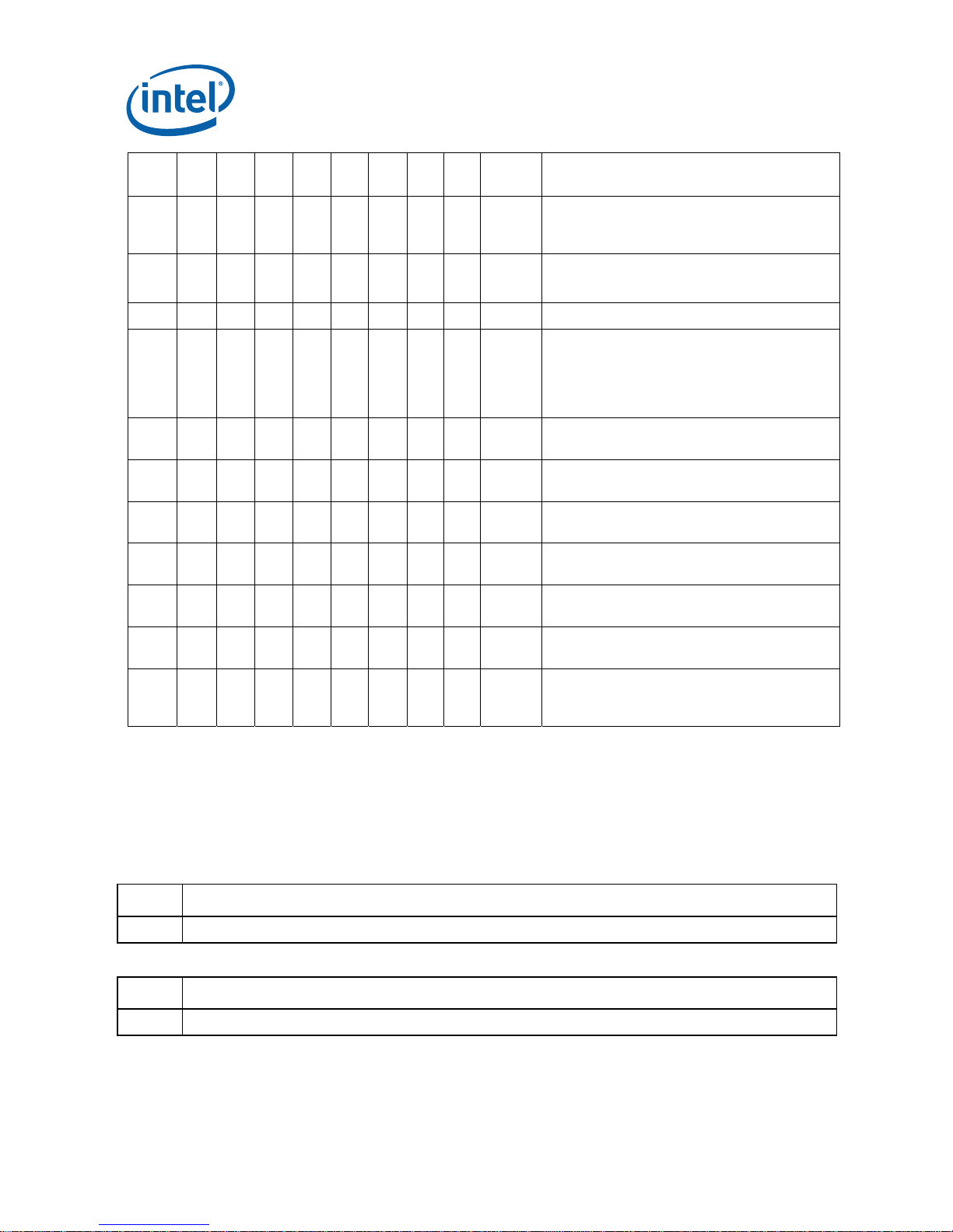
NO. kB0 kC0 cA2 cB0 cC0 cD0 tA1 tB1 Plans ERRATA
E1 X X X X X X X X NoFix
12 Specification Update
FP data operand pointer may be incorrectly
calculated after FP access which wraps
64-Kbyte boundary in 16-bit code
Page 13

Summary Tables of Changes
NO. kB0 kC0 cA2 cB0 cC0 cD0 tA1 tB1 Plans ERRATA
E2 X X X X X X X X NoFix
E3 X X X X X X X X NoFix
E4 X X X X X X X X NoFix
E5 X X X X X X X X NoFix
E6 X X X X X X X X NoFix
E7 X X X X X X X X NoFix BTM for SMI will contain incorrect FROM EIP
E8 X X X X X X X X NoFix
E9 X X X X X X X X NoFix
E10 X X Fixed
E11 X X Fixed
E12 X X X X X X X X NoFix
E13 X X X X X X X X NoFix
E14 X X X X X X X X NoFix LBER may be corrupted after some events
E15 X X X X X X X X NoFix
E16 X X X X X X X X NoFix
E17 X X X X X X X X NoFix
E18 X X X X X X X X NoFix
E19 X X Fixed
E20 X X X X X X X X NoFix
E21 X X X X X X X X NoFix
E22 X X X X X X X X NoFix
E23 X X X X X X X X NoFix
Differences exist in debug exception
reporting
FLUSH# servicing delayed while waiting for
STARTUP_IPI in 2-way MP systems
Code fetch matching disabled debug register
may cause debug exception
Double ECC error on read may result in
BINIT#
FP inexact-result exception flag may not be
set
I/O restart in SMM may fail after
simultaneous MCE
Branch traps do not function if BTMs are also
enabled
Checker BIST failure in FRC mode not
signaled
BINIT# assertion causes FRCERR assertion in
FRC mode
Machine check exception handler may not
always execute successfully
MCE due to L2 parity error gives L1
MCACOD.LL
BTMs may be corrupted during simultaneous
L1 cache line replacement
EFLAGS discrepancy on a page fault after a
multiprocessor TLB shootdown
Near CALL to ESP creates unexpected EIP
address
Memory type undefined for nonmemory
operations
Infinite snoop stall during L2 initialization of
MP systems
FP data operand pointer may not be zero
after power on or Reset
MOVD following zeroing instruction can cause
incorrect result
Premature execution of a load operation
prior to exception handler invocation
Read portion of RMW instruction may
execute twice
Specification Update 13
Page 14

Summary Tables of Changes
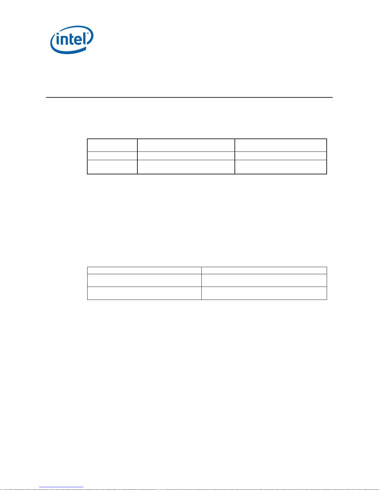
NO. kB0 kC0 cA2 cB0 cC0 cD0 tA1 tB1 Plans ERRATA
MC2_STATUS MSR has model-specific error
E24 X X X X X X X X NoFix
E25 X X X X X X X X NoFix
E26 X X X X X X X X NoFix
E27 X X X X X X X X NoFix
E28 X X X X X X X X NoFix
E29 X X X X X X X X NoFix
E30 X X X X X X X X NoFix
E31 X X X X X X X X NoFix
E32 X X Fixed
E33 X X X X X X X X NoFix
E34 X Fixed
E35 X Fixed Transmission error on cache read
E36 X X X X X X X X NoFix
E37 X X X X X X X X NoFix
E38 X X Fixed
E39 X X X X X X X X NoFix
E40 X Fixed
E41 X X X X X X X X NoFix System bus ECC not functional with 2:1 ratio
E42 X X X X X X X X NoFix
E43 X X X X X X X X NoFix
E44 X X X X Fixed
code and machine check architecture error
code reversed
Mixed cacheability of lock variables is
problematic in MP systems
MOV with debug register causes debug
exception
Upper four PAT entries not usable with Mode
B or Mode C paging
Data breakpoint exception in a displacement
relative near call may corrupt EIP
RDMSR and WRMSR to invalid MSR may not
cause GP fault
SYSENTER/SYSEXIT instructions can
implicitly load null segment selector to SS
and CS registers
PRELOAD followed by EXTEST does not load
boundary scan data
Far jump to new TSS with D-bit cleared may
cause system hang
INT 1 instruction handler execution could
generate a debug exception
COMISS/UCOMISS may not update EFLAGS
under certain conditions
Potential loss of data coherency during MP
data ownership transfer
Misaligned Locked access to APIC space
results in hang
Floating-point exception signal may be
deferred
Memory ordering based synchronization may
cause a livelock condition in mp systems
System bus address parity generator may
report false AERR#
Processor may assert DRDY# on a write with
no data
GP# fault on WRMSR to
ROB_CR_BKUPTMPDR6
Machine check exception may occur due to
improper line eviction in the IFU
14 Specification Update
Page 15

Summary Tables of Changes
NO. kB0 kC0 cA2 cB0 cC0 cD0 tA1 tB1 Plans ERRATA
E45 X X X Fixed
E46 X X X X X Fixed Snoop request may cause DBSY# hang
E47 X X X X X X X X NoFix
E48 X X X Fixed
E49 X X X X X X X X NoFix
E50 X Fixed
E51 X Fixed Noise sensitivity issue on processor SMI# pin
E52 X Fixed
E53 X Fixed
E54 X Fixed IFU/DCU deadlock may cause system hang
E55 X Fixed
E56 X X Fixed
E57 X X X X Fixed
E58 X X X X Fixed
E59 X X X X X X X X NoFix
E60 X X X X X X X X NoFix
E61 X Fixed
E62 X X X X X X Fixed
E63 X Fixed
E64 X X Fixed
E65 X X X X X X X X NoFix
Performance counters include Streaming
SIMD Extensions L1 prefetch
Lower bits of SMRAM SMBASE register
cannot be written with an ITP
Task Switch May Cause Wrong PTE and PDE
Access Bit to be Set
Unsynchronized Cross-Modifying code
operations can cause unexpected instruction
execution results
Processor will erroneously report a BIST
failure
Limitation on cache line ECC detection and
correction
L2_LD and L2_M_LINES_OUTM performancemonitoring counters do not work
L2_DBUS_BUSY performance monitoring
counter will not count writes
Incorrect sign may occur on X87 result due
to indefinite QNaN result from streaming
SIMD extensions multiply
Deadlock may occur due to illegalinstruction/page-miss combination
MASKMOVQ instruction interaction with
string operation may cause deadlock
MOVD, CVTSI2SS, or PINSRW Following
Zeroing Instruction Can Cause Incorrect
Result
FLUSH# assertion following STPCLK# may
prevent CPU clocks from stopping
Intermittent failure to assert ADS# during
processor power-on
Floating-point exception condition may be
deferred
THERMTRIP# may not be asserted as
specified
Cache line reads may result in eviction of
invalid data.
Snoop probe during FLUSH# could cause L2
to be left in shared state
Specification Update 15
Page 16

Summary Tables of Changes
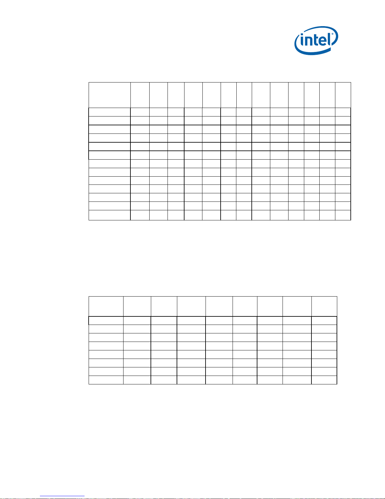
NO. kB0 kC0 cA2 cB0 cC0 cD0 tA1 tB1 Plans ERRATA
E66 X X X X Fixed Livelock may occur due to IFU line eviction
E67 X X X X Fixed
E68 X X X X X X X X NoFix INIT does not clear global entries in the TLB
E69
E70
E71 X X X X X X X X NoFix
E72 X X X X X X X X NoFix
E73 X X X X X X X X NoFix
E74 X X X X X X X X NoFix
E75 X X X X X X X X NoFix
E76 X Fixed
E77 X X X X X X X X PlanFix
E78 X X X X X X X NoFix Incorrect assertion of THERMTRIP# Signal
E79 X NoFix
E80 X X X X X X X1 Fixed
E81 X X X X X X X X NoFix
E82 X X X X X X X X NoFix
E83 X X X X X X X X NoFix IFU/BSU Deadlock May Cause System Hang
E84
X X X X X X X X NoFix VM bit will be cleared on a double fault
X X X X X X X X NoFix Memory aliasing with inconsistent A and D
X X X X X X X X NoFix REP MOVS Operation in Fast string Mode
Selector for the LTR/LLDT register may get
corrupted
handler
bits may cause processor deadlock
Use of memory aliasing with inconsistent
memory type may cause system hang
Processor may report invalid TSS fault
instead of Double fault during mode C
paging
Machine check exception may occur when
interleaving code between different memory
types
Wrong ESP register values during a fault in
VM86 mode
APIC ICR write may cause interrupt not to be
sent when ICR delivery bit pending
High temperature and low supply voltage
operation may result in incorrect processor
operation
During Boundary Scan, BCLK not Sampled
High When SLP# is Asserted Low
Processor might not exit Sleep State
properly upon de-assertion of CPUSLP#
signal
The Instruction Fetch Unit (IFU) may fetch
instructions based upon stale CR3 data after
a write to CR3 register
Under Some Complex Conditions, the
Instructions in the Shadow of a JMP FAR may
be Unintentionally Executed and Retired
Processor Does not Flag #GP on Non-zero
Write to Certain MSRs
Continues in that Mode When Crossing into a
Page with a Different Memory Type
16 Specification Update
Page 17

Summary Tables of Changes
NO. kB0 kC0 cA2 cB0 cC0 cD0 tA1 tB1 Plans ERRATA
X X X X X X X X NoFix The FXSAVE, STOS, MOVS Instructions May
E85
E86 X X X X X X X X NoFix
E87 X X X X X X X X NoFix
E88 X X X X X X X X NoFix
E89 X X X X X X X X NoFix
E90 X X X X X X X X NoFix
E91 X X X X X X X X NoFix
E92 X X X X X X X X NoFix
E93 X X X X X X X X NoFix
E94 X X X X X X X X NoFix
E95 X X X X X X X X NoFix
E96 X X X X X X X X NoFix
E97 X X X X X X X X NoFix
E98 X X X X X X X X NoFix
Cause a Store Ordering Violation When Data
Crosses a Page with a UC Memory Type
POPF and POPFD Instructions that Set the
Trap Flag Bit May Cause Unpredictable
Processor Behavior
Code Segment Limit Violation May Occur on
4 Gbyte Limit Check
FST Instruction with Numeric and Null
Segment Exceptions May Cause General
Protection Faults to be Missed and FP Linear
Address (FLA) Mismatch
Code Segment is Wrong on SMM Handler
when SMBASE is not Aligned
Page with PAT (Page Attribute Table) Set to
USWC (Uncacheable Speculative Write
Combine) While Associated MTRR (Memory
Type Range Register) is UC (Uncacheable)
May Consolidate to UC
Under Certain Conditions LTR (Load Task
Register) Instruction May Result in System
Hang
Loading from Memory Type USWC
(Uncacheable Speculative Write Combine)
May Get Its Data Internally Forwarded From
a Previous Pending Store
FXSAVE after FNINIT Without an Intervening
FP (Floating Point) Instruction May Save
Uninitialized Values for FDP (x87 FPU
Instruction Operand (Data) Pointer Offset)
and FDS (x87 FPU Instruction Operand
(Data) Pointer Selector)
FSTP (Floating Point Store) Instruction Under
Certain Conditions May Result In Erroneously
Setting a Valid Bit on an FP (Floating Point)
Stack Register
Invalid Entries in Page-Directory-PointerTable-Register (PDPTR) May Cause General
Protection (#GP) Exception if the Reserved
Bits are Set to One
Writing the Local Vector Table (LVT)
when an Interrupt is Pending May Cause an
Unexpected Interrupt
The Processor May Report a #TS Instead of
a #GP Fault
A Write to an APIC Register Sometimes May
Appear to Have Not Occurred
Specification Update 17
Page 18
Summary Tables of Changes
NO. kB0 kC0 cA2 cB0 cC0 cD0 tA1 tB1 Plans ERRATA
Using 2M/4M Pages When A20M# Is
E99 X X X X X X X X NoFix
Asserted May Result in Incorrect Address
Translations
E100 X X X X X X X X NoFix
E101 X X X X X X X X NoFix INIT Does Not Clear Global Entries in the TLB
E102 X X X X X X X X NoFix
E103 X X X X X X X X NoFix
E104 X X X X X X X X NoFix
E105 X X X X X X X X NoFix
E106 X X X X X X X X NoFix
E107 X X X X X X X X NoFix
E108 X X X X X X X X NoFix
E109 X X X X X X X X NoFix
Values for LBR/BTS/BTM will be Incorrect
after an Exit from SMM
REP MOVS/STOS Executing with Fast Strings
Enabled and Crossing Page Boundaries with
Inconsistent Memory Types may use an
Incorrect Data Size or Lead to MemoryOrdering Violations
The BS Flag in DR6 May be Set for NonSingle-Step #DB Exception
Fault on ENTER Instruction May Result in
Unexpected Values on Stack Frame
Unaligned Accesses to Paging Structures May
Cause the Processor to Hang
INVLPG Operation for Large (2M/4M) Pages
May be Incomplete under Certain Conditions
Page Access Bit May be Set Prior to
Signaling a Code Segment Limit Fault
EFLAGS, CR0, CR4 and the EXF4 Signal May
be Incorrect after Shutdown
Performance Monitoring Event
FP_MMX_TRANS_TO_MMX May Not Count
Some Transitions
* Fix will be only on Pentium® III processors with CPUID=068xh and not
CPUID=067xh
Notes:
1-
For these steppings, this erratum may be worked around in BIOS.
Number SPECIFICATION CHANGES
There are no Specification Changes in this revision of the Specification Update.
Number SPECIFICATION CLARIFICATIONS
E1 Specification clarification with respect to time stamp counter.
18 Specification Update
Page 19

Summary Tables of Changes
Number DOCUMENTATION CHANGES
There are no Documentation Chnages in this revision of the Specification Update
§
Specification Update 19
Page 20
Identification Information
Identification Informati o n
Component Iden tification via Pr ogramming Interface
The Pentium® III processor can be identified by the following values:
Family1 Model2 Brand ID3
0110 0111 00h = Not Supported
0110 1000 02h = "Intel® Pentium® III
Processor"
NOTES:
1. The Family corresponds to bits [11:8] of the EDX register after RESET, bits [11:8] of
the EAX register after the CPUID instruction is executed with a 1 in the EAX register,
and the generation field of the Device ID register accessible through Boundary Scan.
2. The Model corresponds to bits [7:4] of the EDX register after RESET, bits [7:4] of the
EAX register after the CPUID instruction is executed with a 1 in the EAX register, and
the model field of the Device ID register accessible through Boundary Scan.
3. The Brand ID corresponds to bits [7:0] of the EBX register after the CPUID instruction is
executed with a 1 in the EAX register.
The Pentium III processor’s second level (L2) cache size can be determined by the
following register contents:
512-Kbyte Unified L2 Cache1 43h
256-Kbyte 8 way set associative
32byte line size, L2 Cache
512-Kbyte 8 way set associative
32byte line size, L2 Cache
NOTES:
1. For the Pentium III processor, the unified L2 cache size corresponds to a token in the
EDX register after the CPUID instruction is executed with a 2 in the EAX register. Other
Intel microprocessor models or families may move this information to other bit positions
or otherwise reformat the result returned by this instruction; generic code should parse
the resulting token stream according to the definition of the CPUID instruction.
1
1
82h
83h
20 Specification Update
Page 21

Identification Information
Mixed Step pings i n DP Systems
Intel Corporation fully supports mixed steppings of Pentium III processors. The following list and
processor matrix describes the requirements to support mixed steppings:
• Mixed steppings are only supported with processors that have identical family and model
number as indicated by the CPUID instruction.
• While Intel has done nothing to specifically prevent processors operating at differing
frequencies from functioning within a multiprocessor system, there may be uncharacterized
errata that exist in such configurations. Intel does not support such configurations. In mixed
stepping systems, all processors must operate at identical frequencies (i.e., the highest
frequency rating commonly supported by all processors).
• While there are no known issues associated with the mixing of processors with differing
cache sizes in a dual processor system, and Intel has done nothing to specifically prevent
such system configurations from operating, Intel does not support such configurations since
there may be uncharacterized errata that exist. In dual processor systems, all processors
must be of the same cache size.
• While Intel believes that certain customers may wish to perform validation of system
configurations with mixed frequency or cache sizes, and that those efforts are an acceptable
option to our customers, customers would be fully responsible for the validation of such
configurations.
• The workarounds identified in this and following specification updates must be properly
applied to each processor in the system. Certain errata are specific to the dual processor
environment and are identified in the Mixed Stepping Processor Matrix found at the end of
this section. Errata for all processor steppings will affect system performance if not properly
worked around. Also see the “Pentium® III Processor Identification and Package
Information” table for additional details on which processors are affected by specific errata.
• In dual processor systems, the processor with the lowest feature-set, as determined by the
CPUID Feature Bytes, must be the Bootstrap Processor (BSP). In the event of a tie in
feature-set, the tie should be resolved by selecting the BSP as the processor with the lowest
stepping as determined by the CPUID instruction.
In the following processor matrix a number indicates that a known issue has been identified as
listed in the table following the matrix. A dual processor system using mixed processor steppings
must assure that errata are addressed appropriately for each processor.
Specification Update 21
Page 22

MHz
MHz
MHz
MHz
MHz
MHz
600E
MHz
MHz
MHz
MHz
MHz
550E
600E
MHz
MHz
MHz
MHz
MHz
MHz
600E
MHz
MHz
MHz
MHz
MHz
MHz
1 GHz
Identification Information
DP Platform Population Matrix for t he Pentium® III Processor with 100-MHz System Bus in the SECC and SECC2
Packages
Pentium® III
Processor
Stepping
450-MHz kB0 NI X NI X X X X X X X X X X X X X X X X X X X X X X
500-MHz kB0 X NI X NI X X X X X X X X X X X X X X X X X X X X X
450-MHz kC0 NI X NI X X X X X X X X X X X X X X X X X X X X X X
500-MHz kC0 X NI X NI X X X X X X X X X X X X X X X X X X X X X
550-MHz kC0 X X X X NI X X X X X X X X X X X X X X X X X X X X
600-MHz kC0 X X X X X NI X X X X X X X X X X X X X X X X X X X
600E-MHz cA2 X X X X X X NI X X X X X NI X X X X X NI X X X X X X
650-MHz cA2 X X X X X X X NI X X X X X NI X X X X X NI X X X X X
700-MHz cA2 X X X X X X X X NI X X X X X NI X X X X X NI X X X X
750-MHz cA2 X X X X X X X X X NI X X X X X NI X X X X X NI X X X
800 MHz cA2 X X X X X X X X X X NI X X X X X NI X X X X X NI X X
550E MHz cB0 X X X X X X X X X X X NI X X X X X X X X X X X X X
600E MHz cB0 X X X X X X NI X X X X X NI X X X X X NI X X X X X X
650 MHz cB0 X X X X X X X NI X X X X X NI X X X X X NI X X X X X
700 MHz cB0 X X X X X X X X NI X X X X X NI X X X X X NI X X X X
750 MHz cB0 X X X X X X X X X NI X X X X X NI X X X X X NI X X X
800 MHz cB0 X X X X X X X X X X NI X X X X X NI X X X X X NI X X
850 MHz cB0 X X X X X X X X X X X X X X X X X NI X X X X X NI X
600E-MHz cC0 X X X X X X NI X X X X X NI X X X X X NI X X X X X X
650 MHz cC0 X X X X X X X NI X X X X X NI X X X X X NI X X X X X
700 MHz cC0 X X X X X X X X NI X X X X X NI X X X X X NI X X X X
750-MHz cC0 X X X X X X X X X NI X X X X X NI X X X X X NI X X X
800 MHz cC0 X X X X X X X X X X NI X X X X X NI X X X X X NI X X
850 MHz cC0 X X X X X X X X X X X X X X X X X NI X X X X X NI X
1 GHz cC0 X X X X X X X X X X X X X X X X X X X X X X X X NI
450
kB0
500
kB0
450
kC0
500
kC0
550
kC0
600
kC0
cA2
650
cA2
700
cA2
750
cA2
800
cA2
MHz
cB0
cB0
650
cB0
700
cB0
750
cB0
800
cB0
850
cB0
cC0
650
cC0
700
cC0
750
cC0
800
cC0
850
cC0
cC0
NOTES:
1. X = Mixing processors at different frequencies is not supported. This
stepping/frequency not supported in DP.
2. NI = Currently no known issues associated with mixing these steppings.
22 Specification Update
Page 23
Identification Information
DP Platform Population Matrix for the Pentium® III Processor with 133-MHz
System Bus in the SECC and SECC2 Package from 533MHz to 733MHz
Pentium® III
Processor
Stepping
533B-MHz kB0 NI NI X
533B-MHz kC0 NI NI X
600B-MHz kC0 X X NI
533EB-MHz cA2 X X X
600EB-MHz cA2 X X X
667-MHz cA2 X X X
733-MHz cA2 X X X
533EB MHz cB0 X X X
600EB MHz cB0 X X X
667 MHz cB0 X X X
733 MHz cB0 X X X
600EB-MHz cC0 X X X
667-MHz cC0 X X X
733-MHz cC0 X X X
533B
MHz
kB0
533B
MHz
kC0
533E
600E
667
733
533E
600E
667
600B
B MHz
B MHz
MHz
MHz
B MHz
MHz
cA2
cA2
cA2
kC0
X X X X X X X X X X X
X X X X X X X X X X X
X X X X X X X X X X X
NI X X X NI X X X X X X
X NI X X X NI X X NI X X
X X NI X X
X X X NI
NI X X X NI
X NI
X X NI
X X X NI X X X NI X X NI
X NI X X X NI X X NI X X
X X NI X X X NI X X NI X
X X X NI X X X NI X X NI
cA2
X X
X X
B MHz
cB0
cB0
X
X X
X X X
X NI
X NI X X NI X
733
MHz
MHz
cB0
NI X X NI X
X NI X X NI
X X
B MHz
cB0
600E
667
733
MHz
cC0
MHz
cC0
cC0
X X X
NI X X
NOTES:
1. X = Mixing processors at different frequencies is not supported. This
stepping/frequency is not supported in Dual Processor.
2. NI = Currently no known issues associated with mixing these steppings.
DP Platform Population Matrix for the Pentium® III Processor with 133-MHz
System Bus in the SECC and SECC2 Package from 800MHz to 1.13GHz
Pentium® III Processor
Stepping
800EB-MHz cA2
800EB MHz cB0
866 MHz cB0
933 MHz cB0
1B GHz cB0
800EB MHz cC0
866 MHz cC0
933 MHz cC0
1B GHz cC0
1.13 GHz cC0
800EB
MHz cA2
NI NI X X X NI X X X X
NI NI X X X NI X X X X
NI NI X X X NI X X X X
NOTES:
1. X = Mixing processors at different frequencies is not supported. This
stepping/frequency is not supported in Dual Processor.
2. NI = Currently no known issues associated with mixing these steppings.
800EB
MHz cB0
X X NI X X X NI X X X
X X X NI X X X NI X X
X X X X X X X X X X
X X NI X X X NI X X X
X X X NI X X X NI X X
X X X X X X X X NI X
X X X X X X X X X X
866 MHz
cB0
933
MHz
cB0,
1B GHz
cB0
800EB
MHz cC0
866
MHz
cC0,
933 MHz
cC0,
1B
GHz
cC0
1.13
GHz cC0
Specification Update 23
Page 24

Identification Information
DP Platform Population Matrix for the Pentium® III Processor with 100MHz System Bus in the FC-PGA370 Package from 500 MHz to 650 MHz
Pentium® III
Processor
Stepping
500E-MHz cB0 NI X X X
500E MHz
cB0
550E MHz
cB0
600E MHz
cB0
650 MHz
cB0
600E MHz
cC0
650 MHz
cC0
600E MHz
cD0
X X X
550E-MHz cB0 X NI X X
X X X
600E-MHz cB0 X X NI X
X X NI
650-MHz cB0 X X X NI
X X X
600E-MHz cC0 X X X X NI
X NI
650-MHz cC0 X X X X
X
600E-MHz cD0 X X X X
NI
X
NI
NI X
DP Platform Population Matrix for the Pentium® III Processor with 100-MHz System
Bus in the FC-PGA 370 Pin Package from 700 MHz to 1.10 GHz
Pentium® III
Processor
Stepping
700-MHz cB0 NI X X X NI X X X X NI X X X X X X
750-MHz cB0 X NI X X X NI X X X X NI X X X X X
800-MHz cB0 X X NI X X X NI X X X X NI X X X X
850-MHz cB0 X X X NI X X X NI X X X X NI X X X
700-MHz cC0 NI X X X NI X X X X NI X X X X X X
750-MHz cC0 X NI X X X NI X X X X NI X X X X X
800-MHz cC0 X X NI X X X NI X X X X NI X X X X
850-MHz cC0 X X X NI X X X NI X X X X NI X X X
900-MHz cC0 X X X X X X X X NI X X X X NI X X
700-MHz cD0 NI X X X NI X X X X NI X X X X X X
750-MHz cD0 X NI X X X NI X X X X NI X X X X X
800-MHz cD0 X X NI X X X NI X X X X NI X X X X
850-MHz cD0 X X X NI X X X NI X X X X NI X X X
900-MHz cD0 X X X X X X X X NI X X X X NI X X
1 GHz cD0 X X X X X X X X X X X X X X NI X
1.10GHz cD0 X X X X X X X X X X X X X X X NI
700
750
800
850
700
750
800
850
900
700
750
MHz
MHz
MHz
MHz
MHz
MHz
MHz
MHz
MHz
cB0
cB0
cB0
cB0
cC0
cC0
cC0
cC0
NOTES:
1. X = Mixing processors at different frequencies is not supported.
2. NI = Currently no known issues associated with mixing these steppings.
3. TBD = No issues are expected, however further investigation is required to fully
validate this DP solution.
cC0
MHz
cD0
MHz
cD0
800
MHz
cD0
MHz
850
cD0
900
MHz
cD0
1
GHz
cD0
1.10
GHz
cD0
24 Specification Update
Page 25
800EB
MHz
Identification Information
DP Platform Population Matrix for the Pentium® III Processor with 133MHz System Bus in the FC - PGA370 Packag e from 533 MHz to 800 MHz
Pentium® III
Processor
Stepping
533EB-MHz cB0 NI X X X X X X X X X X X X
600EB-MHz cB0 X NI X X X X X NI X X X X X
667-MHz cB0 X X NI X X X X X NI X X X X
733-MHz cB0 X X X NI X X X X X NI X NI X
800EB-MHz cB0 X X X X NI X X X X X NI X NI
866-MHz cB0 X X X X X NI X X X X X X X
933-MHz cB0 X X X X X X NI X X X X X X
600EB-MHz cC0 X NI X X X X X NI X X X X X
667-MHz cC0 X X NI X X X X X NI X X X X
733-MHz cC0 X X X NI X X X X X NI X X X
800EB-MHz cC0 X X X X NI X X X X X NI X X
733-MHz cD0 X X X X X X X X NI X NI X
800EB-MHz cD0
667
733
866
933
667
733
533EB
600E
MHz
cB0
X X X X NI X X X X X NI X NI
B
MHz
cB0
MHz
cB0
MHz
cB0
800E
B
MHz
cB0
MHz
cB0
MHz
cB0
600E
B
MHz
cC0
MHz
cC0
MHz
cC0
800E
B
MHz
cC0
733
MHz
cD0
cD0
NOTES:
1. X = Mixing processors at different frequencies is not supported.
2. NI = Currently no known issues associated with mixing these steppings.
3. TBD = No issues are expected, however further investigation is required to fully
validate this DP solution.
DP Platform Population Matrix for the Pentium® III
Processor with 133-MHz System Bus in the FC-PGA370
Package from 866 MHz to 1 GHz
Pentium® III
Processor
Stepping
866-MHz cB0
933-MHz cB0
866-MHz cC0
933-MHz cC0
1B-GHz cC0
866-MHz cD0
933-MHz cD0
1B-GHz cD0
NOTES:
1. X = Mixing processors at different frequencies is not supported.
2. NI = Currently no known issues associated with mixing these steppings.
3. TBD = No issues are expected, however further investigation is required to fully
866 MHz
cB0
NI X NI X X NI X X
NI X NI X X NI X X
NI X NI X X NI X X
validate this DP solution.
933 MHz
cB0
X NI X NI X X NI X
X NI X NI X X NI X
X X X X NI X X NI
X NI X NI X X NI X
X X X X NI X X NI
866 MHz
cC0
933 MHz
cC0
1B GHz
cC0
866 MHz
cD0
933 MHz
cD0
1B GHz
cD0
Specification Update 25
Page 26

Identification Information
DP Platform Population Matrix for the Pentium®III Processor with 133-MHz System
Bus in the FC-PGA2 Package from 866 MH z t o 1.4 GH z and uF CBGA2 Package for 800
MHz to 933 MHz
Pentium® III
Processor
Stepping
866-MHz
cD0
933-MHz
cD0
1B-GHz cD0 X X NI X X X X X X X X X X X
1.13-GHz
cD0
800-MHz
tA1
(uFCBGA2)
800-MHz
tB1
(uFCBGA2)
933-MHz
tB1
(uFCBGA2)
1-GHz tA1 X X X X X X X NI X X X X X X
1.13-GHz
tA1
1.26-GHz
tA1
1.4-GHz tA1 X X X X X X X X X X X X NI NI
1.13-GHz
tB1
1.26-GHz
tB1
1.4-GHz tB1 X X X X X X X X X X X X NI NI
866
MHz
cD0
933
MHz
cD0
NI X X X X X X X X X X X X X
X NI X X X X X X X X X X X X
X X X NI X X X X X X X X X X
X X X X NI NI X X X X X X X X
X X X X NI NI X X X X X X X X
X X X X X X NI X X X X X X X
X X X X X X X X NI NI X X X X
X X X X X X X X X X NI NI X X
X X X X X X X X NI NI X X X X
X X X X X X X X X X NI NI X X
1B
GHz
cD0
1.13
GHz
cD0
800
MHz
tA1
800
MHz
tB1
933
MHz
tB1
1
GHz
tA1
1.13
GHz
tA1
1.13
GHz
tB1
1.26
GHz
tA1
1.26
GHz
tB1
1.4
GHz
tA1
1.4
GHz
tB1
NOTES:
1. X = Mixing processors at different frequencies is not supported.
2. NI = Currently no known issues associated with mixing these steppings.
3. TBD = No issues are expected, however further investigation is required to fully
validate this DP solution.
26 Specification Update
Page 27

Identification Information
Pentium® III Processor Identificati on and Package Information
S-Spec
SL364 kB0 0672h 450/100 512 T6P-e/A0 ECC D SECC2† 1, 2, 4
SL365 kB0 0672h 500/100 512 T6P-e/A0 ECC D SECC2† 1, 2, 4, 8
SL3CC kB0 0672h 450/100 512 T6P-e/A0 ECC D SECC2† 1, 2, 3, 4
SL3CD kB0 0672h 500/100 512 T6P-e/A0 ECC D SECC2† 1, 2, 3, 4
SL38E kB0 0672h 450/100 512 T6P-e/A0 ECC D S.E.C.C 1, 2, 4
SL38F kB0 0672h 500/100 512 T6P-e/A0 ECC D S.E.C.C 1, 2, 4
SL35D kC0 0673h 450/100 512 T6P-e/A0 ECC E SECC2† 1, 4
SL37C kC0 0673h 450/100 512 T6P-e/A0 ECC E SECC2† 1, 3, 4
SL35E kC0 0673h 500/100 512 T6P-e/A0 ECC E SECC2† 1, 4
SL37D kC0 0673h 500/100 512 T6P-e/A0 ECC E SECC2† 1, 3, 4
SL3F7 kC0 0673h 550/100 512 T6P-e/A0 ECC E SECC2† 1, 4
SL3FJ kC0 0673h 550/100 512 T6P-e/A0 ECC E SECC2† 1, 3, 4
SL3BN kC0 0673h 533B/133 512 T6P-e/A0 ECC E SECC2† 1, 4, 10
SL3E9 kC0 0673h 533B/133 512 T6P-e/A0 ECC E SECC2† 1, 3, 4, 10
SL3JM kC0 0673h 600/100 512 T6P-e/A0 ECC E SECC2† 1, 4
SL3JT kC0 0673h 600/100 512 T6P-e/A0 ECC E SECC2† 1, 3, 4
SL3JP kC0 0673h 600B/133 512 T6p-e/A0 ECC E SECC2† 1, 4, 10
SL3JU kC0 0673h 600B/133 512 T6P-e/A0 ECC E SECC2† 1, 3, 4, 10
SL3Q9 cA2 0681h 500E/100 256 N/A ECC B FC-PGA
SL3R2 cA2 0681h 500E/100 256 N/A ECC B FC-PGA
SL3VF cA2 0681h 533EB/133 256 N/A ECC B FC-PGA
SL3VA cA2 0681h 533EB/133 256 N/A ECC B FC-PGA
SL3QA cA2 0681h 550E/100 256 N/A ECC B FC-PGA
SL3R3 cA2 0681h 550E/100 256 N/A ECC B FC-PGA
SL3VH cA2 0681h 600E/100 256 N/A ECC B FC-PGA
SL3NL cA2 0681h 600E/100 256 N/A ECC B FC-PGA
Core
Stepping CPUID
Speed
(MHz)
Core/Bus11
L2 Size
(Kbytes)
Tag
RAM/
Stepping
ECC/
Non-
ECC
Processor
Substrate
Revision
Package
and
Revision Notes
9, 10
(370 pin)
7, 9, 10
(370 pin)
9, 10
(370 pin)
7, 9, 10
(370 pin)
9, 10
(370 pin)
7, 9, 10
(370 pin)
9, 10
(370 pin)
7, 9, 10
(370 pin)
Specification Update 27
Page 28

Identification Information
Pentium® III Processor Identificati on and Package Information
S-Spec
Core
Stepping CPUID
Speed
(MHz)
Core/Bus11
L2 Size
(Kbytes)
Tag
RAM/
Stepping
ECC/
Non-
ECC
Processor
Substrate
Revision
Package
and
Revision Notes
SL3VG cA2 0681h 600EB/133 256 N/A ECC B FC-PGA
(370 pin)
SL3VB cA2 0681h 600EB/133 256 N/A ECC B FC-PGA
(370 pin)
SL3VJ cA2 0681h 650/100 256 N/A ECC B FC-PGA
(370 pin)
SL3NM cA2 0681h 650/100 256 N/A ECC B FC-PGA
(370 pin)
SL3VK cA2 0681h 667/133 256 N/A ECC B FC-PGA
(370 pin)
SL3T2 cA2 0681h 667/133 256 N/A ECC B FC-PGA
(370 pin)
SL3VL cA2 0681h 700/100 256 N/A ECC B FC-PGA
(370 pin)
SL3T3 cA2 0681h 700/100 256 N/A ECC B FC-PGA
(370 pin)
SL3VM cA2 0681h 733/133 256 N/A ECC B FC-PGA
(370 pin)
SL3T4 cA2 0681h 733/133 256 N/A ECC B FC-PGA
(370 pin)
SL3VN cA2 0681h 750/100 256 N/A ECC B FC-PGA
(370 pin)
SL3VC cA2 0681h 750/100 256 N/A ECC B FC-PGA
(370 pin)
SL3WB cA2 0681h 800EB/133 256 N/A ECC B FC-PGA
(370 pin)
SL3VE cA2 0681h 800EB/133 256 N/A ECC B FC-PGA
(370 pin)
SL3X4 cA2 0681h 800/100 256 N/A ECC B FC-PGA
(370 pin)
SL3VD cA2 0681h 800/100 256 N/A ECC B FC-PGA
(370 pin)
SL444 cB0 0683h 500E/100 256 N/A ECC B FC-PGA
(370 pin)
SL446 cB0 0683h 500E/100 256 N/A ECC B FC-PGA
(370 pin)
SL45R cB0 0683h 500E/100 256 N/A ECC B FC-PGA
(370 pin)
SL3XS cB0 0683h 533EB/133 256 N/A ECC B FC-PGA
(370 pin)
9, 10
7, 9, 10
9
7, 9
9
7, 9
9
7, 9
9
7, 9
9
7, 9
9, 10
7, 9, 10
9, 10
7, 9, 10
10
10
10, 7
10
28 Specification Update
Page 29

Identification Information
Pentium® III Processor Identificati on and Package Information
S-Spec
Core
Stepping CPUID
Speed
(MHz)
Core/Bus11
L2 Size
(Kbytes)
Tag
RAM/
Stepping
ECC/
Non-
ECC
Processor
Substrate
Revision
Package
and
Revision Notes
SL45S cB0 0683h 533EB/133 256 N/A ECC B FC-PGA
(370 pin)
SL44G cB0 0683h 550E/100 256 N/A ECC B FC-PGA
(370 pin)
SL45T cB0 0683h 550E/100 256 N/A ECC B FC-PGA
(370 pin)
SL3XT cB0 0683h 600EB/133 256 N/A ECC B FC-PGA
(370 pin)
SL45V cB0 0683h 600EB/133 256 N/A ECC B FC-PGA
(370 pin)
SL3XU cB0 0683h 600E/100 256 N/A ECC B FC-PGA
(370 pin)
SL45U cB0 0683h 600E/100 256 N/A ECC B FC-PGA
(370 pin)
SL3XV cB0 0683h 650/100 256 N/A ECC B FC-PGA
(370 pin)
SL45W cB0 0683h 650/100 256 N/A ECC B FC-PGA
(370 pin)
SL3XW cB0 0683h 667/133 256 N/A ECC B FC-PGA
(370 pin)
SL45X cB0 0683h 667/133 256 N/A ECC B FC-PGA
(370 pin)
SL3XX cB0 0683h 700/100 256 N/A ECC B FC-PGA
(370 pin)
SL45Y cB0 0683h 700/100 256 N/A ECC B FC-PGA
(370 pin)
SL45Z cB0 0683h 733/133 256 N/A ECC B FC-PGA
(370 pin)
SL3XY cB0 0683h 733/133 256 N/A ECC B FC-PGA
(370 pin)
SL3XZ cB0 0683h 750/100 256 N/A ECC B FC-PGA
(370 pin)
SL462 cB0 0683h 750/100 256 N/A ECC B FC-PGA
(370 pin)
SL3Y2 cB0 0683h 800EB/133 256 N/A ECC B FC-PGA
(370 pin)
SL464 cB0 0683h 800EB/133 256 N/A ECC B FC-PGA
(370 pin)
SL3Y3 cB0 0683h 800/100 256 N/A ECC B FC-PGA
(370 pin)
10, 7
7
10, 7
10
10, 7
10
10, 7
7
7
7
7
7
10
7, 10
10
Specification Update 29
Page 30

Identification Information
Pentium® III Processor Identificati on and Package Information
S-Spec
Core
Stepping CPUID
Speed
(MHz)
Core/Bus11
L2 Size
(Kbytes)
Tag
RAM/
Stepping
ECC/
Non-
ECC
Processor
Substrate
Revision
Package
and
Revision Notes
SL463 cB0 0683h 800/100 256 N/A ECC B FC-PGA
(370 pin)
SL43H cB0 0683h 850/100 256 N/A ECC B FC-PGA
(370 pin)
SL49G cB0 0683h 850/100 256 N/A ECC B FC-PGA
(370 pin)
SL43J cB0 0683h 866/133 256 N/A ECC B FC-PGA
(370 pin)
SL49H cB0 0683h 866/133 256 N/A ECC B FC-PGA
(370 pin)
SL44J cB0 0683h 933/133 256 N/A ECC B FC-PGA
(370 pin)
SL4CM cC0 0686h 600E/100 256 N/A ECC C FC-PGA
(370 pin)
SL4CL cC0 0686h 600EB/133 256 N/A ECC C FC-PGA
(370 pin)
SL4CK cC0 0686h 650/100 256 N/A ECC C FC-PGA
(370 pin)
SL4CJ cC0 0686h 667/133 256 N/A ECC C FC-PGA
(370 pin)
SL4CH cC0 0686h 700/100 256 N/A ECC C FC-PGA
(370 pin)
SL4M7 cC0 0686h 700/100 256 N/A ECC C FC-PGA
(370 pin)
SL4CG cC0 0686h 733/133 256 N/A ECC C FC-PGA
(370 pin)
SL4M8 cC0 0686h 733/133 256 N/A ECC C FC-PGA
(370 pin)
SL4CF cC0 0686h 750/100 256 N/A ECC C FC-PGA
(370 pin)
SL4M9 cC0 0686h 750/100 256 N/A ECC C FC-PGA
(370 pin)
SL4CE cC0 0686h 800/100 256 N/A ECC C FC-PGA
(370 pin)
SL4MA cC0 0686h 800/100 256 N/A ECC C FC-PGA
(370 pin)
SL4CD cC0 0686h 800EB/133 256 N/A ECC C FC-PGA
(370 pin)
SL4MB cC0 0686h 800EB/133 256 N/A ECC C FC-PGA
(370 pin)
7, 10
7
7
7, 13
7, 13
7, 13
7, 13
7, 13
30 Specification Update
Page 31

Identification Information
Pentium® III Processor Identificati on and Package Information
S-Spec
Core
Stepping CPUID
Speed
(MHz)
Core/Bus11
L2 Size
(Kbytes)
Tag
RAM/
Stepping
ECC/
Non-
ECC
Processor
Substrate
Revision
Package
and
Revision Notes
SL4CC cC0 0686h 850/100 256 N/A ECC C FC-PGA
(370 pin)
SL4MC cC0 0686h 850/100 256 N/A ECC C FC-PGA
(370 pin)
SL4CB cC0 0686h 866/133 256 N/A ECC C FC-PGA
(370 pin)
SL4MD cC0 0686h 866/133 256 N/A ECC C FC-PGA
(370 pin)
SL4SD cC0 0686h 900/100 256 N/A ECC C FC-PGA
(370 pin)
SL4C9 cC0 0686h 933/133 256 N/A ECC C FC-PGA
(370 pin)
SL4ME cC0 0686h 933/133 256 N/A ECC C FC-PGA
(370 pin)
SL4C8 cC0 0686h 1B GHz/133 256 N/A ECC C FC-PGA
(370 pin)
SL4MF cC0 0686h 1B GHz/133 256 N/A ECC C FC-PGA
(370 pin)
SL4WM cC0 0686h 1B GHz/133 256 N/A ECC C FC-PGA
(370 pin)
SL5BT cD0 068Ah 600E/100 256 N/A ECC C FC-PGA
(370 pin)
SL4ZM cD0 068Ah 700/100 256 N/A ECC C FC-PGA
(370 pin)
SL4ZL cD0 068Ah 733/133 256 N/A ECC C FC-PGA
(370 pin)
SL4Z4 cD0 068Ah 750/100 256 N/A ECC C FC-PGA
(370 pin)
SL4ZN cD0 068Ah 800/100 256 N/A ECC C FC-PGA
(370 pin)
SL52P cD0 068Ah 800EB/133 256 N/A ECC C FC-PGA
(370 pin)
SL5QD cD0 068Ah 800EB/133 256 N/A ECC C FC-PGA 2
(370 pin)
SL4Z2 cD0 068Ah 850/100 256 N/A ECC C FC-PGA
(370 pin)
SL49G cD0 068Ah 850/100 256 N/A ECC C FC-PGA
(370 pin)
SL5BS cD0 068Ah 900/100 256 N/A ECC C FC-PGA
(370 pin)
7, 13
7, 13
7, 15
15
16
N/A
17
17
17
17
17
17
17
7, 17
17
Specification Update 31
Page 32

Identification Information
Pentium® III Processor Identificati on and Package Information
S-Spec
Core
Stepping CPUID
Speed
(MHz)
Core/Bus11
L2 Size
(Kbytes)
Tag
RAM/
Stepping
ECC/
Non-
ECC
Processor
Substrate
Revision
Package
and
Revision Notes
SL4ZJ cD0 068Ah 866/133 256 N/A ECC C FC-PGA
(370 pin)
SL49H cD0 068Ah 866/133 256 N/A ECC C FC-PGA
(370 pin)
SL5B5/ cD0 068Ah 866/133 256 N/A ECC C FC-PGA
(370 pin)
SL5DX cD0 068Ah 866/133 256 N/A ECC C FC-PGA
(370 pin)
SL5QE cD0 068Ah 866/133 256 N/A ECC C FC-PGA
(370 pin)
SL52Q cD0 068Ah 933/133 256 N/A ECC C FC-PGA
(370 pin)
SL5DW cD0 068Ah 933/133 256 N/A ECC C FC-PGA
(370 pin)
SL5U3 cD0 068Ah 933MHz
/133
SL5QV cD0 068Ah 1GHz /100 256 N/A ECC C FC-PGA
SL52R cD0 068Ah 1BGHz/133 256 N/A ECC C FC-PGA
SL4F9 cD0 068Ah 1BGHz/133 256 N/A ECC C FC-PGA
SL5DV cD0 068Ah 1BGHz/133 256 N/A ECC C FC-PGA
SL5QW cD0 068Ah 1.10GHz
/100
SL5B3 cD0 068Ah 1BGHz/133 256 N/A ECC C FC-PGA 2
SL5FQ cD0 068Ah 1BGHz/133 256 N/A ECC C FC-PGA 2
SL5B5 cD0 068Ah 866/133 256 N/A ECC C FC-PGA 2
SL5QF cD0 068Ah 933/133 256 N/A ECC C FC-PGA
SL5QJ cD0 068Ah 1B GHz/133 256 N/A ECC C FC-PGA2
SL4YV cD0 068Ah 1.13
GHz/133
SL5B2 cD0 068Ah 1.13
GHz/133
256 N/A ECC C FC-PGA2
(370 pin)
(370 pin)
(370 pin)
(370 pin)
(370 pin)
256 N/A ECC C FC-PGA
(370 pin)
(370 pin)
(370 pin)
(370 pin)
(370 pin)
(370 pin)
256 N/A ECC C FC-PGA2
(370 pin)
256 N/A ECC C FC-PGA2
(370 pin)
17
7, 17
7, 17
7, 17
17, 18
17
7, 17
17
17
7, 17
7, 17
19
7, 19
7, 17
17, 18
18, 19
19
17
32 Specification Update
Page 33

Identification Information
Pentium® III Processor Identificati on and Package Information
S-Spec
Core
Stepping CPUID
Speed
(MHz)
Core/Bus11
L2 Size
(Kbytes)
Tag
RAM/
Stepping
ECC/
Non-
ECC
Processor
Substrate
Revision
Package
and
Revision Notes
SL4YV cD0 068Ah 1.13
GHz/133
SL5QK cD0 068Ah 1.13GHz/13
3
SL5GN tA1 06B1h 1.2GHz /133 256 N/A ECC FC-PGA2
SL5PM tA1 06B1h 1.2GHz /133 256 N/A ECC FC-PGA2
SL5GQ tA1 06B1h 1.13GHz/13
3
SL5LT tA1 06B1h 1.13GHz/13
3
SL5VX tA1 06B1h 1.333GHz
/133
SL64W tA1 06B1h
SL5GR tA1 06B1h 1GHz /133 256 N/A ECC FC-PGA2
SL66D tA1 06B1h 800 MHz-S
SL6HC tB1 06B4h 800 MHz-S
SL5PU tA1 06B1h 1.13GHz-S
SL5LV tA1 06B1h 1.13GHz-S
SL5QL tA1 06B1h 1.26 GHz-S
SL5LW tA1 06B1h 1.26 GHz-S
SL5LV tA1 06B1h 1.13GHz-S
SL657 tA1 06B1h 1.4 GHz-S
SL6BW tB1 06B4h 1.13GHz-S
SL6BX tB1 06B4h 1.26GHz-S
SL6BY tB1 06B4h 1.4GHz-S
1.40
GHz/133
/133
/133
/133
/133
/133
/133
/133
/133
/133
/133
/133
256 N/A ECC C FC-PGA
xxxiii(370
pin)
256 N/A ECC C FC-PGA2
(370 pin)
(370 pin)
(370 pin)
256 N/A ECC FC-PGA2
(370 pin)
256 N/A ECC FC-PGA2
(370 pin)
256 N/A ECC FC-PGA2
(370 pin)
256 No ECC FC-PGA2 9
(370 pin)
512 N/A ECC uFC-BGA 20, 21
512 N/A ECC uFC-BGA 20, 21
512 N/A ECC FC-PGA2
(370 pin)
512 N/A ECC FC-PGA2
(370 pin)
512 N/A ECC FC-PGA2
(370 pin)
512 N/A ECC FC-PGA2
(370 pin)
512 N/A ECC FC-PGA2
(370 pin)
512 N/A ECC FC-PGA2
(370 pin)
512 N/A ECC FC-PGA2
(370 pin)
512 N/A ECC FC-PGA2
(370 pin)
512 N/A ECC FC-PGA2
(370 pin)
17
18, 19,20
9
7, 9
9
7, 9
9
9
20
7, 20
20
7, 20
7, 20
7, 20
20
20
20
Specification Update 33
Page 34

Identification Information
Pentium® III Processor Identificati on and Package Information
S-Spec
SL3H7 cA2 0681h 600EB/133 256 N/A ECC B SECC2 10,20
SL3NB cA2 0681h 600EB/133 256 N/A ECC B SECC2 8,10,7,20
SL3KV cA2 0681h 650/100 256 N/A ECC B SECC2 10,7, 20
SL3NR cA2 0681h 650/100 256 N/A ECC B SECC2 8,10, 20
SL3KW cA2 0681h 667/133 256 N/A ECC B SECC2 7, 20
SL3SY cA2 0681h 700/100 256 N/A ECC B SECC2 8,10
SL3SB cA2 0681h 700/100 256 N/A ECC B SECC2 8,10
SL3S9 cA2 0681h 700/100 256 N/A ECC B SECC2 8,10
SL3SZ cA2 0681h 733/133 256 N/A ECC B SECC2 8,10
SL3H6 cA2 0681h 600E/100 256 N/A ECC B SECC2 8,10
Core
Stepping CPUID
Speed
(MHz)
Core/Bus11
L2 Size
(Kbytes)
Tag
RAM/
Stepping
ECC/
Non-
ECC
Processor
Substrate
Revision
Package
and
Revision Notes
SL3SB cA2 0681h 733/133 256 N/A ECC B SECC2 8,10
SL3ND cA2 0681h 667/133 256 N/A ECC B SECC2 8,10
SL3N6 cA2 0681h 533EB/133 256 N/A ECC B SECC2 8,10
SL3SX cA2 0681h 533EB/133 256 N/A ECC B SECC2 8,10
SL3V5 cA2 0681h 550E/100 256 N/A ECC B SECC2 8,10
SL3N7 cA2 0681h 550E/100 256 N/A ECC B SECC2 8,10
SL3NA cA2 0681h 600E/100 256 N/A ECC B SECC2 8,10
SL3WC cA2c 0681h 750/100 256 N/A ECC B SECC2 8,10
SL3V6 cA2 0681h 750/100 256 N/A ECC B SECC2 8,10
SL3Z6 cA2 0681h 800/100 256 N/A ECC B SECC2 8,10
SL3V7 cA2 0681h 800/100 256 N/A ECC B SECC2 8,10
SL3WA cA2 0681h 800EB/133 256 N/A ECC B SECC2 8,10
SL3V8 cA2 0681h 800EB/133 256 N/A ECC B SECC2 8,10
SL4G7 cA2 0681h 800EB/133 256 N/A ECC B SECC2 8,10
SL3XG cB0 0683h 533EB/133 256 N/A ECC B SECC2 8, 10
SL44W cB0c 0683h 533EB/133 256 N/A ECC B SECC2 8,10
SL3XH cB0 0683h 550E/100 256 N/A ECC B SECC2 8,10
SL44X cB0 0683h 550E/100 256 N/A ECC B SECC2 8,10
SL43E cB0 0683h 600E/100 256 N/A ECC B SECC2 8,10
SL44Y cB0 0683h 600E/100 256 N/A ECC B SECC2 8,10
34 Specification Update
Page 35

Identification Information
Pentium® III Processor Identificati on and Package Information
S-Spec
SL3XJ cB0 0683h 600EB/133 256 N/A ECC B SECC2 8, 10
SL44Z cB0 0683h 600EB/133 256 N/A ECC B SECC2 8, 10
SL3XK cB0 0683h 650/100 256 N/A ECC B SECC2 8, 10
SL452 cB0 0683h 650/100 256 N/A ECC B SECC2 8, 10
SL3XL cB0 0683h 667/133 256 N/A ECC B SECC2 8, 10
SL453 cB0 0683h 667/133 256 N/A ECC B SECC2 8, 10
SL3XM cB0 0683h 700/100 256 N/A ECC B SECC2 8, 10
SL454 cB0 0683h 700/100 256 N/A ECC B SECC2 8, 10
SL3XN cB0 0683h 733/133 256 N/A ECC B SECC2 8, 10
SL455 cB0 0683h 733/133 256 N/A ECC B SECC2 8, 10
Core
Stepping CPUID
Speed
(MHz)
Core/Bus11
L2 Size
(Kbytes)
Tag
RAM/
Stepping
ECC/
Non-
ECC
Processor
Substrate
Revision
Package
and
Revision Notes
SL3XP cB0 0683h 750/100 256 N/A ECC B SECC2 8, 10
SL456 cB0 0683h 750/100 256 N/A ECC B SECC2 8, 10
SL3XQ cB0 0683h 800EB/133 256 N/A ECC B SECC2 8, 10
SL458 cB0 0683h 800EB/133 256 N/A ECC B SECC2 8, 10
SL3XR cB0 0683h 800/100 256 N/A ECC B SECC2 8, 10
SL457 cB0 0683h 800/100 256 N/A ECC B SECC2 8, 10
SL43F cB0 0683h 850/100 256 N/A ECC B SECC2 8, 10
SL47M cB0 0683h 850/100 256 N/A ECC B SECC2 8, 10
SL43G cB0 0683h 866/133 256 N/A ECC B SECC2 8, 10
SL47N cB0 0683h 866/133 256 N/A ECC B SECC2 8, 10
SL448 cB0 0683h 933/133 256 N/A ECC B SECC2 8, 10
SL47Q cB0 0683h 933/133 256 N/A ECC B SECC2 8, 10
SL4FP cB0 0683h 1B GHz/133 256 N/A ECC B SECC2 8, 10
SL48S cB0 0683h 1B GHz /133 256 N/A ECC B SECC2 8, 10
SL4C7 cC0 0686h 600E/100 256 N/A ECC B SECC2 8, 10
SL4C6 cC0 0686h 600EB/133 256 N/A ECC B SECC2 8, 10
SL4C5 cC0 0686h 650/100 256 N/A ECC B SECC2 8, 10
SL4C4 cC0 0686h 667/133 256 N/A ECC B SECC2 8, 10
SL4C3 cC0 0686h 700/100 256 N/A ECC B SECC2 8, 10
SL4C2 cC0 0686h 733/133 256 N/A ECC B SECC2 8, 10
Specification Update 35
Page 36

Identification Information
Pentium® III Processor Identificati on and Package Information
S-Spec
SL4KD cC0 0686h 733/133 256 N/A ECC B SECC2 8, 10
SL4FQ cC0 0686h 733/133 256 N/A ECC B SECC2 8, 10
SL4BZ cC0 0686h 750/100 256 N/A ECC B SECC2 8, 10
SL4BY cC0 0686h 800/100 256 N/A ECC B SECC2 8, 10
SL4KF cC0 0686h 800/100 256 N/A ECC B SECC2 8, 10
SL4BX cC0 0686h 800EB/133 256 N/A ECC B SECC2 8, 10
SL4G7 cC0 0686h 800EB/133 256 N/A ECC B SECC2 8, 10
SL4KG cC0 0686h 800EB/133 256 N/A ECC B SECC2 8, 10
SL4BW cC0 0686h 850/100 256 N/A ECC B SECC2 8, 10
SL4KH cC0 0686h 850/100 256 N/A ECC B SECC2 8, 10
Core
Stepping CPUID
Speed
(MHz)
Core/Bus11
L2 Size
(Kbytes)
Tag
RAM/
Stepping
ECC/
Non-
ECC
Processor
Substrate
Revision
Package
and
Revision Notes
SL4BV cC0 0686h 866/133 256 N/A ECC B SECC2 8, 10
SL4KJ cC0 0686h 866/133 256 N/A ECC B SECC2 8, 10
SL4BT cC0 0686h 933/133 256 N/A ECC B SECC2 8, 10
SL4KK cC0 0686h 933/133 256 N/A ECC B SECC2 8, 10
SL4BR cC0 0686h 1 GHz/100 256 N/A ECC C SECC2 15
SL4KL cC0 0686h 1 GHz/100 256 N/A ECC C SECC2 8
SL4BS cC0 0686h 1B GHz/133 256 N/A ECC C SECC2 10,15
SL4HH cC0 0686h 1.13
GHz/133
SL69K tB1 06B4h 933 MHz-
S/133
SL6QU tB1 06B4h 1Ghz 512 N/A ECC N/A uFC-BGA 20,21
†
Unless otherwise noted, all Pentium III processors in S.E.C.C.2 package have an OLGA package core.
NOTES:
1. These parts will only operate at the specified core to bus frequency ratio at which they
were manufactured and tested. It is not necessary to configure the core frequency
ratios by using the A20M#, IGNEE#, LINT[1]/NMI and LINT[0]/INTR pins during RESET.
2. These processors will not shut down automatically upon assertion of THERMTRIP#.
3. This is a boxed processor with an attached heatsink.
4. Performance-monitoring event counters do not reflect MOVD and MOVQ stores to
memory on these processors.
5. These parts will not assert THERMTRIP#, nor will they shut down in the event of an
over-temperature condition (e.g., Tj = ~135 C).
6. Pin AJ3 is removed from these parts.
7. This is a boxed processor with an unattached fan heatsink.
8. This is a boxed processor with an attached fan heatsink.
9. These processors will not be validated in Dual Processor (DP) applications.
256 N/A ECC C SECC2 12,8
512 N/A ECC N/A uFC-BGA 20,21
36 Specification Update
Page 37

Identification Information
10. The “E” and “B” designators distinguish between Pentium® III processors with the
same core frequency but different system bus frequencies and/or cache
implementations.
The “E” and “B” designators distinguish between Pentium® III processors with the
same core frequency but different system bus frequencies and/or cache
implementations.
B = 133 MHz System Bus
E = Processors with “Advanced Transfer Cache” (CPUID 068x and greater only if a
frequency overlap exists)
If, for a given core frequency, Pentium III processors are only available with one
system bus frequency and one cache implementation, the above designators will not be
used (e.g., not all processors with “Advanced Transfer Cache” will have the “E”
designation).
11. Speeds will be marked as MHz up to but not including 1GHz. Speeds 1GHz and above
will have the GHz marking.
12. Vcc = 1.80V. Tj = 60C for this 1.13 GHz processor with CPUID 0686.
13. Tj = 80C, Vcc = 1.70v.
14. Vcc = 1.65V.
15. Vcc = 1.70V for these cCX core steppings. Tj = 70C for 1.0 GHz. Tj = 75C for 933
MHz.
16. This SL4WM S-spec part has a VID request of 1.70V, however the processor should be
supplie d 1.76V at the PGA V cc pins. See Pentium® III datasheet for further
information.
17. Vcc=1.75V for cD0 Core Stepping (CPUID 068Ah). Tj=77 C for 933MHz and Tj=75 C
1GHz. Tj=80 C for 866MHz to 700MHz.
18. This processor is valid for low voltage system bus operation at 1.25V AGTL and normal
1.5V AGTL+ signal levels. This processor is also DP capable at the 1.25V AGTL system
bus level. This processor will auto detect differential or single ended clocking.
19. Vcc=1.75V for cD0 Core Stepping (CPUID 068Ah). Tcase=64 C for 1GHz. Tcase = 67
C for 1.13GHz. This package exists as an FC-PGA2 with Integrated Heat Spreader
(IHS).
20. These parts are intended for server design applications.
21. Tualatin LV DP 1.15V, non SpeedStep enabled
Component Marking Information
Pentium® III Processor and Boxed Pentium® III Processor Markings
Dynamic Mark Area
FPO - Serial #
of Assy
Specification Update 37
Country
Speed / Cache / Bus / Voltage
2-D Matrix Mark
UL Identifier
500/ 512/100/2.0V S1
FFFFFFFF-NNNN XXXXX
m
i ©’98 SYYYY
S-Spec
Page 38

Pentium® III Processor Markings
SECC2/Slot 1 Package
FC-PGA 370 Pin Package
Identification Information
Hologram
Location
GRP1LN1: INTEL (m)(c) '01_-_{COO}
GRP1LN2: {Speed}/{Cache}/{Bus}/{Voltage}
FC-PGA2 370 Pin Package
GRP1LN1
GRP1LN2
GRP2LN1
GRP2LN2
GRP2LN1: {FPO}-{S/N}
GRP2LN2: PENTIUM III {S-Spec}
GRP1LN1: INTEL (m)(c) '01_-_{Country of Origin}
GRP1LN2: {Core freq}/{Cache}/{Bus Freq}/{Voltage}
GRP2LN1: {FPO}-{S/N}
GRP2LN2: PENTIUM III {S-Spec} or PENTIUM III-S {S-Spec}
Note: S above applies to 06BxH 512KB cache processor
§
38 Specification Update
Page 39

Errata
Errata
E1. FP Data Operand Pointer May Be Incorrectly Calculated After FP
Access Which Wraps 64 Kbyt e Bound ary in 16 Bit Code
Problem: The FP Data Operand Pointer is the effective address of the operand associated with
the last non-control floating-point instruction executed by the machine. If an 80-bit
floating-point access (load or store) occurs in a 16-bit mode other than protected
mode (in which case the access will produce a segment limit violation), the memory
access wraps a 64-Kbyte boundary, and the floating-point environment is
subsequently saved, the value contained in the FP Data Operand Pointer may be
incorrect.
Implication: A 32-bit operating system running 16-bit floating-point code may encounter this
erratum, under the following conditions:
• The operating system is using a segment greater than 64 Kbytes in size.
• An application is running in a 16-bit mode other than protected mode.
• An 80-bit floating-point load or store which wraps the 64-Kbyte boundary is
executed.
• The operating system performs a floating-point environment store
(FSAVE/FNSAVE/FSTENV/FNSTENV) after the above memory access.
• The operating system uses the value contained in the FP Data Operand Pointer.
Wrapping an 80 bit floating-point load around a segment boundary in this way is not
a normal programming practice. Intel has not currently identified any software which
exhibits this behavior.
Workaround: If the FP Data Operand Pointer is used in an OS which may run 16-bit floating-
point code, care must be taken to ensure that no 80-bit floating-point accesses are
wrapped around a 64-Kbyte boundary
Status: For the steppings affected see the Summary of Changes at the beginning of this
section.
E2. Differences Exist in Debug Exception Reporting
Problem: There exist some differences in the reporting of code and data breakpoint matches
between that specified by previous Intel processor specifications and the behavior of
the processor, as described below:
Case 1: The first case is for a breakpoint set on a MOVSS or POPSS instruction, when
the instruction following it causes a debug register protection fault (DR7.gd
is already set, enabling the fault). The processor reports delayed data
breakpoint matches from the MOVSS or POPSS instructions by setting the
matching DR6.bi bits, along with the debug register protection fault
Specification Update 39
Page 40

Errata
(DR6.bd). If additional breakpoint faults are matched during the call of the
debug fault handler, the processor sets the breakpoint match bits (DR6.bi)
to reflect the breakpoints matched by both the MOVSS or POPSS breakpoint
and the debug fault handler call. The processor only sets DR6.bd in either
situation, and does not set any of the DR6.bi bits.
Case 2: In the second breakpoint reporting failure case, if a MOVSS or POPSS
instruction with a data breakpoint is followed by a store to memory which:
a) crosses a 4-Kbyte page boundary,
OR
b) causes the page table Access or Dirty (A/D) bits to be modified,
the breakpoint information for the MOVSS or POPSS will be lost. Previous
processors retain this information under these boundary conditions.
Case 3: If they occur after a MOVSS or POPSS instruction, the INTn, INTO, and INT3
instructions zero the DR6.bi bits (bits B0 through B3), clearing pending
breakpoint information, unlike previous processors.
Case 4: If a data breakpoint and an SMI (System Management Interrupt) occur
simultaneously, the SMI will be serviced via a call to the SMM handler, and
the pending breakpoint will be lost.
Case 5: When an instruction that accesses a debug register is executed, and a
breakpoint is encountered on the instruction, the breakpoint is reported
twice.
Case 6: Unlike previous versions of Intel Architecture processors, P6 family
processors will not set the Bi bits for a matching disabled breakpoint unless
at least one other breakpoint is enabled.
Implication: When debugging or when developing debuggers for a P6 family processor-based
system, this behavior should be noted. Normal usage of the MOVSS or POPSS
instructions (i.e., following them with a MOV ESP) will not exhibit the behavior of
cases 1-3. Debugging in conjunction with SMM will be limited by case 4.
Workaround: Following MOVSS and POPSS instructions with a MOV ESP instruction when using
breakpoints will avoid the first three cases of this erratum. No workaround has been
identified for cases 4, 5, or 6.
Status: For the steppings affected see the Summary of Changes at the beginning of this
section.
E3. FLUSH# S ervicing Delayed While Waiting for STA RTUP_IPI in 2 way
MP Systems
Problem: In a 2-way MP system, if an application processor is waiting for a startup inter-
processor interrupt (STARTUP_IPI), then it will not service a FLUSH# pin assertion
until it has received the STARTUP_IPI.
Implication: After the 2-way MP initialization protocol, only one processor becomes the bootstrap
processor (BSP). The other processor becomes a slave application processor (AP).
40 Specification Update
Page 41

Errata
After losing the BSP arbitration, the AP goes into a wait loop, waiting for a
STARTUP_IPI.
The BSP can wake up the AP to perform some tasks with a STARTUP_IPI, and then
put it back to sleep with an initialization inter-processor interrupt (INIT_IPI, which
has the same effect as asserting INIT#), which returns it to a wait loop. The result is
a possible loss of cache coherency if the off-line processor is intended to service a
FLUSH# assertion at this point. The FLUSH# will be serviced as soon as the processor
is awakened by a STARTUP_IPI, before any other instructions are executed. Intel has
not encountered any operating systems that are affected by this erratum.
Workaround: Operating system developers should take care to execute a WBINVD instruction
before the AP is taken off-line using an INIT_IPI
Status: For the steppings affected see the Summary of Changes at the beginning of this
section.
E4. Code Fetch Matching Disabled Debug Register May Cause Debug
Exception
Problem: The bits L0 3 and G0 3 enable breakpoints local to a task and global to all tasks,
respectively. If one of these bits is set, a breakpoint is enabled, corresponding to the
addresses in the debug registers DR0-DR3. If at least one of these breakpoints is
enabled, any of these registers are disabled (i.e., Ln and Gn are 0), and RWn for the
disabled register is 00 (indicating a breakpoint on instruction execution), normally an
instruction fetch will not cause an instruction-breakpoint fault based on a match with
the address in the disabled register(s). However, if the address in a disabled register
matches the address of a code fetch which also results in a page fault, an instructionbreakpoint fault will occur.
Implication: The bits L0 3 and G0 3 enable breakpoints local to a task and global to all tasks,
respectively. If one of these bits is set, a breakpoint is enabled, corresponding to the
addresses in the debug registers DR0-DR3. If at least one of these breakpoints is
enabled, any of these registers are disabled (i.e., Ln and Gn are 0), and RWn for the
disabled register is 00 (indicating a breakpoint on instruction execution), normally an
instruction fetch will not cause an instruction-breakpoint fault based on a match with
the address in the disabled register(s). However, if the address in a disabled register
matches the address of a code fetch which also results in a page fault, an instructionbreakpoint fault will occur.
Implication: While debugging software, extraneous instruction-breakpoint faults may be
encountered if breakpoint registers are not cleared when they are disabled. Debug
software which does not implement a code breakpoint handler will fail, if this occurs.
If a handler is present, the fault will be serviced. Mixing data and code may
exacerbate this problem by allowing disabled data breakpoint registers to break on
an instruction fetch.
Workaround: The debug handler should clear breakpoint registers before they become disabled
Status: For the steppings affected see the Summary of Changes at the beginning of this
section.
E5. Double ECC Error on Read May Result in BINIT#
Specification Update 41
Page 42

Errata
Problem: For this erratum to occur, the following conditions must be met:
• Machine Check Exceptions (MCEs) must be enabled.
• A dataless transaction (such as a write invalidate) must be occurring
simultaneously with a transaction which returns data (a normal read).
• The read data must contain a double-bit uncorrectable ECC error.
If these conditions are met, the Pentium III processor will not be able to determine
which transaction was erroneous, and instead of generating an MCE, it will generate
a BINIT#.
Implication: The bus will be reinitialized in this case. However, since a double-bit uncorrectable
ECC error occurred on the read, the MCE handler (which is normally reached on a
double-bit uncorrectable ECC error for a read) would most likely cause the same
BINIT# event.
Workaround: Though the ability to drive BINIT# can be disabled in the Pentium III processor,
which would prevent the effects of this erratum, overall system behavior would not
improve, since the error which would normally cause a BINIT# would instead cause
the machine to shut down. No other workaround has been identified.
Status: For the steppings affected see the Summary of Changes at the beginning of this
section
E6. FP Inexact-Result Exception Flag May Not Be Set
Problem: When the result of a floating-point operation is not exactly representable in the
destination format (1/3 in binary form, for example), an inexact-result (precision)
exception occurs. When this occurs, the PE bit (bit 5 of the FPU status word) is
normally set by the processor. Under certain rare conditions, this bit may not be set
when this rounding occurs. However, other actions taken by the processor (invoking
the software exception handler if the exception is unmasked) are not affected. This
erratum can only occur if the floating-point operation which causes the precision
exception is immediately followed by one of the following instructions:
• FST m32real
• FST m64real
• FSTP m32real
• FSTP m64real
• FSTP m80real
• FIST m16int
• FIST m32int
• FISTP m16int
• FISTP m32int
• FISTP m64int
42 Specification Update
Page 43

Errata
Note that even if this combination of instructions is encountered, there is also a
dependency on the internal pipelining and execution state of both instructions in the
processor.
Implication: Inexact-result exceptions are commonly masked or ignored by applications, as it
happens frequently, and produces a rounded result acceptable to most applications.
The PE bit of the FPU status word may not always be set upon receiving an inexactresult exception. Thus, if these exceptions are unmasked, a floating-point error
exception handler may not recognize that a precision exception occurred. Note that
this is a “sticky” bit, i.e., once set by an inexact-result condition, it remains set until
cleared by software.
Workaround: This condition can be avoided by inserting two NOP instructions between the two
floating-point instructions.
Status: For the steppings affected see the Summary of Changes at the beginning of this
section.
E7. BTM for SMI Will Contain Incorrect FROM EIP
Problem: A system management interrupt (SMI) will produce a Branch Trace Message (BTM), if
BTMs are enabled. However, the FROM EIP field of the BTM (used to determine the
address of the instruction which was being executed when the SMI was serviced) will
not have been updated for the SMI, so the field will report the same FROM EIP as the
previous BTM.
Implication: A BTM which is issued for an SMI will not contain the correct FROM EIP, limiting the
usefulness of BTMs for debugging software in conjunction with System Management
Mode (SMM).
Workaround: None identified.
Status: For the steppings affected see the Summary of Changes at the beginning of this
section.
E8. I/O Restart in SMM May Fail After Simultaneous MCE
Problem: If an I/O instruction (IN, INS, REP INS, OUT, OUTS, or REP OUTS) is being executed,
and if the data for this instruction becomes corrupted, the Pentium III processor will
signal a machine check exception (MCE). If the instruction is directed at a device
which is powered down, the processor may also receive an assertion of SMI#. Since
MCEs have higher priority, the processor will call the MCE handler, and the SMI#
assertion will remain pending. However, upon attempting to execute the first
instruction of the MCE handler, the SMI# will be recognized and the processor will
attempt to execute the SMM handler. If the SMM handler is completed successfully, it
will attempt to restart the I/O instruction, but will not have the correct machine state,
due to the call to the MCE handler.
Implication: A simultaneous MCE and SMI# assertion may occur for one of the I/O instructions
above. The SMM handler may attempt to restart such an I/O instruction, but will have
corrupted state due to the MCE handler call, leading to failure of the restart and
shutdown of the processor.
Specification Update 43
Page 44

Errata
Workaround: If a system implementation must support both SMM and MCEs, the first thing the
SMM handler code (when an I/O restart is to be performed) should do is check for a
pending MCE. If there is an MCE pending, the SMM handler should immediately exit
via an RSM instruction and allow the machine check exception handler to execute. If
there is not, the SMM handler may proceed with its normal operation.
Status: For the steppings affected see the Summary of Changes at the beginning of this
section.
E9. Branch Traps Do Not Function If BTMs Are Also Enabled
Problem: If branch traps or branch trace messages (BTMs) are enabled alone, both function as
expected. However, if both are enabled, only the BTMs will function, and the branch
traps will be ignored.
Implication: The branch traps and branch trace message debugging features cannot be used
together.
Workaround: If branch trap functionality is desired, BTMs must be disabled.
Status: For the steppings affected see the Summary of Changes at the beginning of this
section.
E10. Checker BIST Failure in FRC Mode Not Signaled
Problem: If a system is running in functional redundancy checking (FRC) mode, and the
checker of the master-checker pair encounters a hard failure while running the builtin self test (BIST), the checker will tri-state all outputs without signaling an IERR#.
Implication: Assuming the master passes BIST successfully, it will continue execution unchecked,
operating without functional redundancy. However, the necessary pull-up on the
FRCERR pin will cause an FRCERR to be signaled. The operation of the master
depends on the implementation of FRCERR.
Workaround: For successful detection of BIST failure in the checker of an FRC pair, use the
FRCERR signal, instead of IERR#.
Status: For the steppings affected see the Summary of Changes at the beginning of this
section.
E11. BINIT# Assertion Causes FRCERR Assertion in FRC Mode
Problem: If a pair of Pentium III processors are running in functional redundancy checking
(FRC) mode, and a catastrophic error condition causes BINIT# to be asserted, the
checker in the master-checker pair will enter shutdown. The next bus transaction
from the master will then result in the assertion of FRCERR.
Implication: Bus initialization via an assertion of BINIT# occurs as the result of a catastrophic
error condition which precludes the continuing reliable execution of the system.
Under normal circumstances, the master-checker pair would remain synchronized in
the execution of the BINIT# handler. However, due to this erratum, an FRCERR will
be signaled. System behavior then depends on the system specific error recovery
mechanisms.
44 Specification Update
Page 45

Errata
Workaround: None identified.
Status: For the steppings affected see the Summary of Changes at the beginning of this
section.
E12. Machine Check Exception Handler May Not Always Execute
Successfully
Problem: An asynchronous machine check exception (MCE), such as a BINIT# event, which
occurs during an access that splits a 4 Kbyte page boundary, may leave some
internal registers in an indeterminate state. Thus, the MCE handler code may not
always run successfully if an asynchronous MCE has occurred previously.
Implication: An MCE may not always result in the successful execution of the MCE handler.
However, asynchronous MCEs usually occur upon detection of a catastrophic system
condition that would also hang the processor. Leaving MCEs disabled will result in the
condition which caused the asynchronous MCE instead causing the processor to enter
shutdown. Therefore, leaving MCEs disabled may not improve overall system
behavior.
Workaround: No workaround which would guarantee successful MCE handler execution under
this condition has been identified.
Status: For the steppings affected see the Summary of Changes at the beginning of this
section.
E13. MCE Due to L2 Parity Error Gives L1 MCACOD.LL
Problem: If a Cache Reply Parity (CRP) error, Cache Address Parity (CAP) error, or Cache
Synchronous Error (CSER) occurs on an access to the Pentium III processor’s L2
cache, the resulting Machine Check Architectural Error Code (MCACOD) will be logged
with ‘01’ in the LL field. This value indicates an L1 cache error; the value should be
‘10’, indicating an L2 cache error. Note that L2 ECC errors have the correct value of
‘10’ logged.
Implication: An L2 cache access error, other than an ECC error, will be improperly logged as an L1
cache error in MCACOD.LL.
Workaround: None identified.
Status: For the steppings affected see the Summary of Changes at the beginning of this
section.
E14. LBER May Be Corrupted After Some Events
Problem: The last branch record (LBR) and the last branch before exception record (LBER) can
be used to determine the source and destination information for previous branches or
exceptions. The LBR contains the source and destination addresses for the last
branch or exception, and the LBER contains similar information for the last branch
taken before the last exception. This information is typically used to determine the
location of a branch which leads to execution of code which causes an exception.
However, after a catastrophic bus condition which results in an assertion of BINIT#
and the re-initialization of the buses, the value in the LBER may be corrupted. Also,
Specification Update 45
Page 46

Errata
after either a CALL which results in a fault or a software interrupt, the LBER and LBR
will be updated to the same value, when the LBER should not have been updated.
Implication: The LBER and LBR registers are used only for debugging purposes. When this
erratum occurs, the LBER will not contain reliable address information. The value of
LBER should be used with caution when debugging branching code; if the values in
the LBR and LBER are the same, then the LBER value is incorrect. Also, the value in
the LBER should not be relied upon after a BINIT# event.
Workaround: None identified.
Status: For the steppings affected see the Summary of Changes at the beginning of this
section.
E15. BTMs May Be Corrupted During Simultaneous L1 Cache Line
Replacement
Problem: When Branch Trace Messages (BTMs) are enabled and such a message is generated,
the BTM may be corrupted when issued to the bus by the L1 cache if a new line of
data is brought into the L1 data cache simultaneously. Though the new line being
stored in the L1 cache is stored correctly, and no corruption occurs in the data, the
information in the BTM may be incorrect due to the internal collision of the data line
and the BTM.
Implication: Although BTMs may not be entirely reliable due to this erratum, the conditions
necessary for this boundary condition to occur have only been exhibited during
focused simulation testing. Intel has currently not observed this erratum in a system
level validation environment.
Workaround: None identified.
Status: For the steppings affected see the Summary of Changes at the beginning of this
section.
E16. EFLAGS Discrepancy on a Page Fault After a Multiprocessor TLB
Shootdown
Problem: This erratum may occur when the Pentium III processor executes one of the following
read-modify-write arithmetic instructions and a page fault occurs during the store of
the memory operand: ADD, AND, BTC, BTR, BTS, CMPXCHG, DEC, INC, NEG, NOT,
OR, ROL/ROR, SAL/SAR/SHL/SHR, SHLD, SHRD, SUB, XOR, and XADD. In this case,
the EFLAGS value pushed onto the stack of the page fault handler may reflect the
status of the register after the instruction would have completed execution rather
than before it. The following conditions are required for the store to generate a page
fault and call the operating system page fault handler:
1. The store address entry must be evicted from the DTLB by speculative loads from
other instructions that hit the same way of the DTLB before the store has
completed. DTLB eviction requires at least three-load operations that have linear
address bits 15:12 equal to each other and address bits 31:16 different from
each other in close physical proximity to the arithmetic operation.
2. The page table entry for the store address must have its permissions tightened
during the very small window of time between the DTLB eviction and execution of
46 Specification Update
Page 47

Errata
the store. Examples of page permission tightening include from Present to Not
Present or from Read/Write to Read Only, etc.
3. Another processor, without corresponding synchronization and TLB flush, must
cause the permission change.
Implication: This scenario may only occur on a multiprocessor platform running an operating
system that performs “lazy” TLB shootdowns. The memory image of the EFLAGS
register on the page fault handler’s stack prematurely contains the final arithmetic
flag values although the instruction has not yet completed. Intel has not identified
any operating systems that inspect the arithmetic portion of the EFLAGS register
during a page fault nor observed this erratum in laboratory testing of software
applications.
Workaround: No workaround is needed upon normal restart of the instruction, since this
erratum is transparent to the faulting code and results in correct instruction behavior.
Operating systems may ensure that no processor is currently accessing a page that is
scheduled to have its page permissions tightened or have a page fault handler that
ignores any incorrect state.
Status: For the steppings affected see the Summary of Changes at the beginning of this
section.
E17. Near CALL to ESP Creates Unexpected EIP Address
Problem: As documented, the CALL instruction saves procedure linking information in the
procedure stack and jumps to the called procedure specified with the destination
(target) operand. The target operand specifies the address of the first instruction in
the called procedure. This operand can be an immediate value, a general-purpose
register, or a memory location. When accessing an absolute address indirectly using
the stack pointer (ESP) as a base register, the base value used is the value in the
ESP register before the instruction executes. However, when accessing an absolute
address directly using ESP as the base register, the base value used is the value of
ESP after the return value is pushed on the stack, not the value in the ESP register
before the instruction executed.
Implication: Due to this erratum, the processor may transfer control to an unintended address.
Results are unpredictable, depending on the particular application, and can range
from no effect to the unexpected termination of the application due to an exception.
Intel has observed this erratum only in a focused testing environment. Intel has not
observed any commercially available operating system, application, or compiler that
makes use of or generates this instruction.
Workaround: If the other seven general-purpose registers are unavailable for use, and it is
necessary to do a CALL via the ESP register, first push ESP onto the stack, then
perform an indirect call using ESP (e.g., CALL [ESP]). The saved version of ESP
should be popped off the stack after the call returns.
Status: For the steppings affected see the Summary of Changes at the beginning of this
section.
E18. Memory Type Undefined for Nonmemory Operations
Specification Update 47
Page 48

Errata
Problem: The Memory Type field for nonmemory transactions such as I/O and Special Cycles
are undefined. Although the Memory Type attribute for nonmemory operations
logically should (and usually does) manifest itself as UC, this feature is not designed
into the implementation and is therefore inconsistent.
Implication: Bus agents may decode a non-UC memory type for nonmemory bus transactions.
Workaround: Bus agents must consider transaction type to determine the validity of the
Memory Type field for a transaction.
Status: For the steppings affected see the Summary of Changes at the beginning of this
section.
E19. Infinite Snoop Stall During L2 Initialization of MP Systems
Problem: It is possible for snoop traffic generated on the system bus while a processor is
executing its L2 cache initialization routine to cause the initializing processor to hang.
Implication: A DP (2-way) system which does not suppress snoop traffic while L2 caches are being
initialized may hang during this initialization sequence.
The system BIOS can create an execution environment which allows processors to
initialize their L2 caches without the system generating any snoop traffic on the bus.
Below is a pseudo-code fragment, designed explicitly for a two-processor system,
that uses a serial algorithm to initialize each processor’s L2 cache:
Suppress_all_I/O_traffic()
K = 0;
while (K <= 1)
{
/* Obtain current value of K. This forces both Temp and K into */
/* the L1 cache. Note that Temp could also be maintained in a */
/* general purpose register. */
Temp = K;
Wait_until_all_processors_are_signed_in_at_barrier()
if ( logical_proc_APIC_id == K ) {
{
wait_10_usecs_delay_loop(); /* this time delay, required */
/* in the worst case, allows */
/* the barrier semaphore to */
48 Specification Update
Page 49

Errata
/* settle to shared state. */
Initialize L2 cache
K++
}
else
while (Temp == K);
}
}
This algorithm prevents bus snoop traffic from the other processors, which would
otherwise cause the initializing processor to hang. The algorithm assumes that the L1
cache is enabled (the Temp and K variables must be cached by each processor).
Also, the Memory Type Range Register (MTRR) for the data segment must be set to
WB (writeback) memory type.
Status: For the steppings affected see the Summary of Changes at the beginning of this
section.
E20. FP Data Operand Pointer May Not Be Zero After Power On or Reset
Problem: The FP Data Operand Pointer, as specified, should be reset to zero upon power on or
Reset by the processor. Due to this erratum, the FP Data Operand Pointer may be
nonzero after power on or Reset.
Implication: Software which uses the FP Data Operand Pointer and count on its value being zero
after power on or Reset without first executing an FINIT/FNINIT instruction will use
an incorrect value, resulting in incorrect behavior of the software.
Workaround: Software should follow the recommendation in Section 8.2 of the Intel
Architecture Software Developer’s Manual, Volume 3: System Programming Guide
(Order Number 243192). This recommendation states that if the FPU will be used,
software-initialization code should execute an FINIT/FNINIT instruction following a
hardware reset. This will correctly clear the FP Data Operand Pointer to zero.
Status: For the steppings affected see the Summary of Changes at the beginning of this
section.
E21. MOVD Following Zeroing Instruction Can Cause Incorrect Result
Problem: An incorrect result may be calculated after the following circumstances occur:
1. A register has been zeroed with either a SUB reg, reg instruction or an XOR reg,
reg instruction,
2. A value is moved with sign extension into the same register’s lower 16 bits; or a
signed integer multiply is performed to the same register’s lower 16 bits,
3. This register is then copied to an MMX™ technology register using the MOVD
instruction prior to any other operations on the sign-extended value.
Specification Update 49
Page 50

Errata
Specifically, the sign may be incorrectly extended into bits 16-31 of the MMX
technology register. Only the MMX technology register is affected by this erratum.
The erratum only occurs when the three following steps occur in the order shown.
The erratum may occur with up to 40 intervening instructions that do not modify the
sign-extended value between steps 2 and 3.
1. XOR EAX, EAX
or SUB EAX, EAX
2. MOVSX AX, BL
or MOVSX AX, byte ptr <memory address> or MOVSX AX, BX
or MOVSX AX, word ptr <memory address> or IMUL BL (AX implicit, opcode F6
/5)
or IMUL byte ptr <memory address> (AX implicit, opcode F6 /5) or IMUL AX, BX
(opcode 0F AF /r)
or IMUL AX, word ptr <memory address> (opcode 0F AF /r) or IMUL AX, BX, 16
(opcode 6B /r ib)
or IMUL AX, word ptr <memory address>, 16 (opcode 6B /r ib) or IMUL AX, 8
(opcode 6B /r ib)
or IMUL AX, BX, 1024 (opcode 69 /r iw)
or IMUL AX, word ptr <memory address>, 1024 (opcode 69 /r iw) or IMUL AX,
1024 (opcode 69 /r iw)
or CBW
3. MOVD MM0, EAX
Note that the values for immediate byte/words are merely representative (i.e., 8, 16,
1024) and that any value in the range for the size may be affected. Also, note that
this erratum may occur with “EAX” replaced with any 32 bit general-purpose register,
and “AX” with the corresponding 16-bit version of that replacement. “BL” or “BX” can
be replaced with any 8-bit or 16-bit general-purpose register. The CBW and IMUL
(opcode F6 /5) instructions are specific to the EAX register only.
In the example, EAX is forced to contain 0 by the XOR or SUB instructions. Since the
four types of the MOVSX or IMUL instructions and the CBW instruction modify only
bits 15:8 of EAX by sign extending the lower 8 bits of EAX, bits 31:16 of EAX should
always contain 0. This implies that when MOVD copies EAX to MM0, bits 31:16 of
MM0 should also be 0. Under certain scenarios, bits 31:16 of MM0 are not 0, but are
replicas of bit 15 (the 16th bit) of AX. This is noticeable when the value in AX after
the MOVSX, IMUL, or CBW instruction is negative, i.e., bit 15 of AX is a 1.
When AX is positive (bit 15 of AX is a 0), MOVD will always produce the correct
answer. If AX is negative (bit 15 of AX is a 1), MOVD may produce the right answer
or the wrong answer depending on the point in time when the MOVD instruction is
executed in relation to the MOVSX, IMUL, or CBW instruction.
50 Specification Update
Page 51

Errata
Implication: The effect of incorrect execution will vary from unnoticeable, due to the code
sequence discarding the incorrect bits, to an application failure. If the MMX
technology-enabled application in which MOVD is used to manipulate pixels, it is
possible for one or more pixels to exhibit the wrong color or position momentarily. It
is also possible for a computational application that uses the MOVD instruction in the
manner described above to produce incorrect data. Note that this data may cause an
unexpected page fault or general protection fault
Workaround: There are two possible workarounds for this erratum:
1. Rather than using the MOVSX-MOVD, IMUL-MOVD, or CBW-MOVD pairing to
handle one variable at a time, use the sign extension capabilities (PSRAW, etc.)
within MMX technology for operating on multiple variables. This would result in
higher performance as well.
2. Insert another operation that modifies or copies the sign-extended value between
the MOVSX/IMUL/CBW instruction and the MOVD instruction as in the example
below:
XOR EAX, EAX (or SUB EAX, EAX)
MOVSX AX, BL (or other MOVSX, other IMUL or CBW instruction)
*MOV EAX, EAX
MOVD MM0, EAX
*Note: MOV EAX, EAX is used here as it is fairly generic. Again, EAX can be any 32bit register.
Status: For the steppings affected see the Summary of Changes at the beginning of this
section.
E22. Premature Execution of a Load Operation Prior to Exception Handler
Invocation
Problem: This erratum can occur with any of the following situations:
1. If an instruction that performs a memory load causes a code segment limit
violation,
2. If a waiting floating-point instruction or MMX™ instruction that performs a
memory load has a floating-point exception pending, or
3. If an MMX instruction that performs a memory load and has either CR0.EM =1
(Emulation bit set), or a floating-point Top-of-Stack (FP TOS) not equal to 0, or a
DNA exception pending.
If any of the above circumstances occur it is possible that the load portion of the
instruction will have executed before the exception handler is entered.
Implication: In normal code execution where the target of the load operation is to write back
memory there is no impact from the load being prematurely executed, nor from the
restart and subsequent re-execution of that instruction by the exception handler. If
the target of the load is to uncached memory that has a system side-effect,
Specification Update 51
Page 52

Errata
restarting the instruction may cause unexpected system behavior due to the
repetition of the side-effect.
Workaround: Code which performs loads from memory that has side-effects can effectively
workaround this behavior by using simple integer-based load instructions when
accessing side-effect memory and by ensuring that all code is written such that a
code segment limit violation cannot occur as a part of reading from side-effect
memory.
Status: For the steppings affected see the Summary of Changes at the beginning of this
section.
E23. Read Portion of RMW Instruction May Execute Twice
Problem: When the Pentium III processor executes a read-modify-write (RMW) arithmetic
instruction, with memory as the destination, it is possible for a page fault to occur
during the execution of the store on the memory operand after the read operation
has completed but before the write operation completes.
If the memory targeted for the instruction is UC (uncached), memory will observe the
occurrence of the initial load before the page fault handler and again if the instruction
is restarted.
Implication: This erratum has no effect if the memory targeted for the RMW instruction has no
side-effects. If, however, the load targets a memory region that has side-effects,
multiple occurrences of the initial load may lead to unpredictable system behavior.
Workaround: Hardware and software developers who write device drivers for custom hardware
that may have a side-effect style of design should use simple loads and simple stores
to transfer data to and from the device. Then, the memory location will simply be
read twice with no additional implications.
Status: For the steppings affected see the Summary of Changes at the beginning of this
section.
E24. MC2_STATUS MSR Has Model-Specific Error Code and Machine Check
Architecture Error Code Reversed
Problem: The Intel Architecture Software Developer’s Manual, Volume 3: System Programming
Guide, documents that for the MCi_STATUS MSR, bits 15:0 contain the MCA
(machine-check architecture) error code field, and bits 31:16 contain the modelspecific error code field. However, for the MC2_STATUS MSR, these bits have been
reversed. For the MC2_STATUS MSR, bits 15:0 contain the model-specific error code
field and bits 31:16 contain the MCA error code field.
Implication: A machine check error may be decoded incorrectly if this erratum on the
MC2_STATUS MSR is not taken into account.
Workaround: When decoding the MC2_STATUS MSR, reverse the two error fields.
Status: For the steppings affected see the Summary of Changes at the beginning of this
section.
E25. Mixed Cacheability of Lock Variables Is Problematic in MP Systems
52 Specification Update
Page 53

Errata
Problem: This errata only affects multiprocessor systems where a lock variable address is
marked cacheable in one processor and uncacheable in any others. The processors
which have it marked uncacheable may stall indefinitely when accessing the lock
variable. The stall is only encountered if:
• One processor has the lock variable cached, and is attempting to execute a cache
lock.
• If the processor which has that address cached has it cached in its L2 only.
• Other processors, meanwhile, issue back to back accesses to that same address
on the bus.
Implication: MP systems where all processors either use cache locks or consistent locks to
uncacheable space will not encounter this problem. If, however, a lock variable’s
cacheability varies in different processors, and several processors are all attempting
to perform the lock simultaneously, an indefinite stall may be experienced by the
processors which have it marked uncacheable in locking the variable (if the conditions
above are satisfied). Intel has only encountered this problem in focus testing with
artificially generated external events. Intel has not currently identified any
commercial software which exhibits this problem.
Workaround: Follow a homogenous model for the memory type range registers (MTRRs),
ensuring that all processors have the same cacheability attributes for each region of
memory; do not use locks whose memory type is cacheable on one processor, and
uncacheable on others. Avoid page table aliasing, which may produce a
nonhomogenous memory model.
Status: For the steppings affected see the Summary of Changes at the beginning of this
section.
E26. MOV With Debug Register Causes Debug Exception
Problem: When in V86 mode, if a MOV instruction is executed on debug registers, a general-
protection exception (#GP) should be generated, as documented in the Intel
Architecture Software Developer's Manual, Volume 3: System Programming Guide,
Section 14.2. However, in the case when the general detect enable flag (GD) bit is
set, the observed behavior is that a debug exception (#DB) is generated instead.
Implication: With debug-register protection enabled (i.e., the GD bit set), when attempting to
execute a MOV on debug registers in V86 mode, a debug exception will be generated
instead of the expected general-protection fault.
Workaround: In general, operating systems do not set the GD bit when they are in V86 mode.
The GD bit is generally set and used by debuggers. The debug exception handler
should check that the exception did not occur in V86 mode before continuing. If the
exception did occur in V86 mode, the exception may be directed to the generalprotection exception handler.
Status: For the steppings affected see the Summary of Changes at the beginning of this
section.
E27. Upper Four PAT Entries Not Usable With Mode B or Mode C Paging
Specification Update 53
Page 54

Errata
Problem: The Page Attribute Table (PAT) contains eight entries, which must all be initialized
and considered when setting up memory types for the Pentium III processor.
However, in Mode B or Mode C paging, the upper four entries do not function
correctly for 4-Kbyte pages. Specifically, bit 7 of page table entries that translate
addresses to 4-Kbyte pages should be used as the upper bit of a 3-bit index to
determine the PAT entry that specifies the memory type for the page. When Mode B
(CR4.PSE = 1) and/or Mode C (CR4.PAE) are enabled, the processor forces this bit to
zero when determining the memory type regardless of the value in the page table
entry. The upper four entries of the PAT function correctly for 2-Mbyte and 4-Mbyte
large pages (specified by bit 12 of the page directory entry for those translations).
Implication: Only the lower four PAT entries are useful for 4-KB translations when Mode B or C
paging is used. In Mode A paging (4-Kbyte pages only), all eight entries may be
used. All eight entries may be used for large pages in Mode B or C paging.
Workaround: None identified
Status: For the steppings affected see the Summary of Changes at the beginning of this
section.
E28. Dat a Breakpoint Exce ption in a Displace ment Relative Near Call May
Corrupt EIP
Problem: If a misaligned data breakpoint is programmed to the same cache line as the
memory location where the stack push of a near call is performed and any data
breakpoints are enabled, the processor will update the stack and ESP appropriately,
but may skip the code at the destination of the call. Hence, program execution will
continue with the next instruction immediately following the call, instead of the target
of the call.
Implication: The failure mechanism for this erratum is that the call would not be taken; therefore,
instructions in the called subroutine would not be executed. As a result, any code
relying on the execution of the subroutine will behave unpredictably.
Workaround: Whether enabled or not, do not program a misaligned data breakpoint to the
same cache line on the stack where the push for the near call is performed.
Status: For the steppings affected see the Summary of Changes at the beginning of this
section.
E29. RDMSR or WRMSR to Invalid MSR Address May Not Cause GP F a ul t
Problem: The RDMSR and WRMSR instructions allow reading or writing of MSRs (Model Specific
Registers) based on the index number placed in ECX. The processor should reject
access to any reserved or unimplemented MSRs by generating #GP(0). However,
there are some invalid MSR addresses for which the processor will not generate
#GP(0).
Implication: For RDMSR, undefined values will be read into EDX:EAX. For WRMSR, undefined
processor behavior may result.
Workaround: Do not use invalid MSR addresses with RDMSR or WRMSR.
54 Specification Update
Page 55

Errata
Status: For the steppings affected see the Summary of Changes at the beginning of this
section
E30. SYSENTER/SYSEXIT Instructions Can Implicitly Load “Null Segment
Selector” to SS and CS Reg isters
Problem: According to the processor specification, attempting to load a null segment selector
into the CS and SS segment registers should generate a General Protection Fault
(#GP). Although loading a null segment selector to the other segment registers is
allowed, the processor will generate an exception when the segment register holding
a null selector is used to access memory.
However, the SYSENTER instruction can implicitly load a null value to the SS segment
selector. This can occur if the value in SYSENTER_CS_MSR is between FFF8h and
FFFBh when the SYSENTER instruction is executed. This behavior is part of the
SYSENTER/SYSEXIT instruction definition; the content of the SYSTEM_CS_MSR is
always incremented by 8 before it is loaded into the SS. This operation will set the
null bit in the segment selector if a null result is generated, but it does not generate a
#GP on the SYSENTER instruction itself. An exception will be generated as expected
when the SS register is used to access memory, however.
The SYSEXIT instruction will also exhibit this behavior for both CS and SS when
executed with the value in SYSENTER_CS_MSR between FFF0h and FFF3h, or
between FFE8h and FFEBh, inclusive.
Implication: These instructions are intended for operating system use. If this erratum occurs (and
the OS does not ensure that the processor never has a null segment selector in the
SS or CS segment registers), the processor’s behavior may become unpredictable,
possibly resulting in system failure.
Workaround: Do not initialize the SYSTEM_CS_MSR with the values between FFF8h and FFFBh,
FFF0h and FFF3h, or FFE8h and FFEBh before executing SYSENTER or SYSEXIT.
Status: For the steppings affected see the Summary of Changes at the beginning of this
section.
E31. PRELOAD Followed by EXTEST Does Not Load Boundary Scan Data
Problem: According to the IEEE 1149.1 Standard, the EXTEST instruction would use data
“typically loaded onto the latched parallel outputs of boundary-scan shift-register
stages using the SAMPLE/PRELOAD instruction prior to the selection of the EXTEST
instruction.” As a result of this erratum, this method cannot be used to load the data
onto the outputs.
Implication: Using the PRELOAD instruction prior to the EXTEST instruction will not produce
expected data after the completion of EXTEST.
Workaround: None identified
Status: For the steppings affected see the Summary of Changes at the beginning of this
section.
E32. Far Jump to New TSS With D-bit Cleared May Cause System Hang
Specification Update 55
Page 56

Errata
Problem: A task switch may be performed by executing a far jump through a task gate or to a
new Task State Segment (TSS) directly. Normally, when such a jump to a new TSS
occurs, the D-bit (which indicates that the page referenced by a Page Table Entry
(PTE) has been modified) for the PTE which maps the location of the previous TSS will
already be set, and the processor will operate as expected. However, if the D-bit is
clear at the time of the jump to the new TSS, the processor will hang.
Implication: If an OS is used which can clear the D-bit for system pages, and which jumps to a
new TSS on a task switch, then a condition may occur which results in a system
hang. Intel has not identified any commercial software which may encounter this
condition; this erratum was discovered in a focused testing environment.
Workaround: Ensure that OS code does not clear the D-bit for system pages (including any
pages that contain a task gate or TSS). Use task gates rather than jumping to a new
TSS when performing a task switch.
Status: For the steppings affected see the Summary of Changes at the beginning of this
section.
E33. INT 1 Instruction Handler Execution Could Generate a Debug
Exception
Problem: If the processor’s general detect enable flag is set and an explicit call is made to the
interrupt procedure via the INT 1 instruction, the general detect enable flag should be
cleared prior to entering the handler. As a result of this erratum, the flag is not
cleared prior to entering the handler. If an access is made to the debug registers
while inside of the handler, the state of the general detect enable flag will cause a
second debug exception to be taken. The second debug exception clears the general
detect enable flag and returns control to the handler which is now able to access the
debug registers.
Implication: This erratum will generate an unexpected debug exception upon accessing the debug
registers while inside of the INT 1 handler.
Workaround: Ignore the second debug exception that is taken as a result of this erratum.
Status: For the steppings affected see the Summary of Changes at the beginning of this
section.
E34. COMISS/UCOMISS May Not Update Eflags Under Certain Conditions
Problem: COMISS/UCOMISS instructions compare the least significant pairs of packed single-
precision floating-point numbers and set the ZF, PF, and CF bits in the EFLAGS
register accordingly (the OF, SF, and AF bits are cleared). Under certain conditions
when a memory location is loaded into cache, the EFLAGS may not get set.
Implication: The result of the incorrect status of the EFLAGS may range from no effect to an
unexpected application/OS behavior.
Workaround: It is possible for BIOS code to contain a workaround for this erratum.
Status: For the steppings affected see the Summary of Changes at the beginning of this
section.
56 Specification Update
Page 57

Errata
E35. Transmission Error on Cache Read
Problem: During reads of the L2 cache, the processor may use certain L2 cache optimizations
that may result in a data transmission error
Implication: Data corruption caused by this erratum will result in unpredictable system behavior.
Workaround: It is possible for BIOS code to contain a workaround for this erratum.
Status: For the steppings affected see the Summary of Changes at the beginning of this
section.
E36. Potential Loss of Data Coherency During MP Data Ownershi p Transfer
Problem: In MP systems, processors may be sharing data in different cache lines, referenced
as line A and line B in the discussion below. When this erratum occurs (with the
following example given for a 2-way MP system with processors noted as ‘P0’ and
‘P1’), P0 contains a shared copy of line B in its L1. P1 has a shared copy of Line A.
Each processor must manage the necessary invalidation and snoop cycles before that
processor can modify and source the results of any internal writes to the other
processor.
There exists a narrow timing window when, if P1 requests a coy of line B it may be
supplied by P0 in an Exclusive state which allows P1 to modify the contents of the line
with no further external invalidation cycles. In this narrow window P0 may also retire
instructions that use the original data present before P1 performed the modification
Implication: Multiprocessor or threaded application synchronization, required for low-level data
sharing, that is implemented via operating system provided synchronization
constructs are not affected by this erratum. Applications which rely upon the usage of
locked semaphores rather than memory ordering are also unaffected. Uniprocessor
systems are not affected by this erratum. If the erratum does occur one processor
may execute software with the stale data that was present from the previous shared
state rather than the data written more recently by another processor.
Workaround: Deterministic barriers beyond which program variables will not be modified can
be achieved via the usage of locked semaphore operations. These should effectively
prevent the occurrence of this erratum
Status: For the steppings affected see the Summary of Changes at the beginning of this
section.
E37. Misaligned Locked Access to APIC Space Results in Hang
Problem: When the processor’s APIC space is accessed with a misaligned locked access a
machine check exception is expected. However, the processor’s machine check
architecture is unable to handle the misaligned locked access.
Implication: If this erratum occurs the processor will hang. Typical usage models for the APIC
address space do not use locked accesses. This erratum will not affect systems using
such a model.
Workaround: Ensure that all accesses to APIC space are aligned.
Specification Update 57
Page 58

Errata
Status: For the steppings affected see the Summary of Changes at the beginning of this
section.
E38. Floating-Point Exception Sig nal May Be Deferred
Problem: A one clock window exists where a pending x87 FP exception that should be signaled
on the execution of a CVTPS2PI, CVTPI2PS, or CVTTPS2PI instruction may be
deferred to the next waiting floating-point instruction or instruction that would
change MMX™ register state.
Implication: If this erratum occurs the floating-point exception will not be handled as expected.
Workaround: Applications that follow Intel programming guidelines (empty all x87 registers
before executing MMX technology instructions) will not be affected by this erratum
Status: For the steppings affected see the Summary of Changes at the beginning of this
section
E39. Memory Ordering Based Synchronization May Cause a Livelock
Condition in MP Systems
Problem: In an MP environment, the following sequence of code (or similar code) in two
processors (P0 and P1) may cause them to each enter an infinite loop (livelock
condition):
P0 P1
MOV [xyz], EAX (1) wait1: MOV EBX, [abc] (2)
. CMP EBX, val1 (3)
. JNE wait1 (4)
.
MOV [abc], val1 (6) MOV [abc], val2 (5)
wait0: MOV EBX, [abc] (7)
CMP EBX, val2 (8)
JNE wait0 (9)
NOTE
The EAX and EBX can be any general-purpose register. Addresses [abc] and [xyz]
can be any location in memory and must be in the same bank of the L1 cache.
Variables “val1” and “val2” can be any integer.
The algorithm above involves processors P0 and P1, each of which use loops to keep
them synchronized with each other. P1 is looping until instruction (6) in P0 is globally
observed. Likewise, P0 will loop until instruction (5) in P1 is globally observed.
58 Specification Update
Page 59

Errata
The P6 architecture allows for instructions (1) and (7) in P0 to be dispatched to the
L1 cache simultaneously. If the two instructions are accessing the same memory
bank in the L1 cache, the load (7) will be given higher priority and will complete,
blocking instruction (1).
Instructions (8) and (9) may then execute and retire, placing the instruction pointer
back to instruction (7). This is due to the condition at the end of the “wait0” loop
being false. The livelock scenario can occur if the timing of the wait0 loop execution is
such that instruction (7) in P0 is ready for completion every time that instruction (1)
tries to complete. Instruction (7) will again have higher priority, preventing the data
([xyz]) in instruction (1) from being written to the L1 cache. This causes instruction
(6) in P0 to not complete and the sequence “wait0” to loop infinitely in P0.
A livelock condition also occurs in P1 because instruction (6) in P0 does not complete
(blocked by instruction (1) not completing). The problem with this scenario is that P0
should eventually allow for instruction (1) to write its data to the L1 cache. If this
occurs, the data in instruction (6) will be written to memory, allowing the conditions
in both loops to be true.
Implication: Both processors will be stuck in an infinite loop, leading to a hang condition. Note
that if P0 receives any interrupt, the loop timing will be disrupted such that the
livelock will be broken. The system timer, a keystroke, or mouse movement can
provide an interrupt that will break the livelock.
Workaround: Use a LOCK instruction to force P0 to execute instruction (6) before instruction
(7).
Status: For the steppings affected see the Summary of Changes at the beginning of this
section.
E40. System Bus Address Parity Generator May Report Fa l se AERR#
Problem: The processor’s address parity error detection circuit may fail to meet its frequency
timing specification under certain environmental conditions. At the high end of the
temperature specification and/or the low end of the voltage range, the processor may
report false address parity errors.
Implication: If the system has AERR# drive enabled (bit [3] of the EBL_CR_POWERON resister set
to ‘1’) spurious address detection and reporting may occur. In some system
configurations, BINIT# may be asserted on the system bus. This may cause some
systems to generate a machine check exception and in others may cause a reboot.
Workaround: Disable AERR# drive from the processor. AERR# drive may be disabled by
clearing bit [3] in the EBL_CR_POWERON register. In addition, if the chipset allows,
AERR# drive should be enabled from the chipset and AERR# observation enabled on
the processor. AERR# observation on the processor is enabled by asserting A8# on
the active-to-inactive transition of RESET#.
Status: For the processor part numbers affected see the “Pentium® III Processor
Identification and Packaging Information” table in the General Information section.
E41. System Bus ECC Not Functional With 2:1 Ratio
Specification Update 59
Page 60

Errata
Problem: If a processor is underclocked at a core frequency to system bus frequency ratio of
2:1 and system bus ECC is enabled, the system bus ECC detection and correction will
negatively affect internal timing dependencies.
Implication: If system bus ECC is enabled, and the processor is underclocked at a 2:1 ratio, the
system may behave unpredictably due to these timing dependencies.
Workaround: All bus agents that support system bus ECC must disable it when a 2:1 ratio is
used.
Status: For the steppings affected see the Summary of Changes at the beginning of this
section.
E42. Processor May Assert DRDY# on a Write With No Data
Problem: When a MASKMOVQ instruction is misaligned across a chunk boundary in a way that
one chunk has a mask of all 0’s, the processor will initiate two partial write
transactions with one having all byte enables deasserted. Under these conditions, the
expected behavior of the processor would be to perform both write transactions, but
to deassert DRDY# during the transaction which has no byte enables asserted. As a
result of this erratum, DRDY# is asserted even though no data is being transferred.
Implication: The implications of this erratum depend on the bus agent’s ability to handle this
erroneous DRDY# assertion. If a bus agent cannot handle a DRDY# assertion in this
situation, or attempts to use the invalid data on the bus during this transaction,
unpredictable system behavior could result
Workaround: A system which can accept a DRDY# assertion during a write with no data will not
be affected by this erratum. In addition, this erratum will not occur if the MASKMOVQ
is aligned.
Status: For the steppings affected see the Summary of Changes at the beginning of this
section.
E43. GP# Fault on WRMSR to ROB_CR_BKUPTMPDR6
Problem: Writing a ‘1’ to unimplemented bit(s) in the ROB_CR_BKUPTMPDR6 MSR (offset 1E0h)
will result in a general protection fault (GP#).
Implication: The normal process used to write an MSR is to read the MSR using RDMSR, modify
the bit(s) of interest, and then to write the MSR using WRMSR. Because of this
erratum, this process may result in a GP# fault when used to modify the
ROB_CR_BKUPTMPDR6 MSR.
Workaround: When writing to ROB_CR_BKUPTMPDR6 all unimplemented bits must be ‘0.’
Implemented bits may be set as ‘0’ or ‘1’ as desired.
Status: For the steppings affected see the Summary of Changes at the beginning of this
section.
E44. Machine Check Exception May Occur Due to Improper Line Eviction in
the IFU
60 Specification Update
Page 61

Errata
Problem: The Pentium III processor is designed to signal an unrecoverable Machine Check
Exception (MCE) as a consistency checking mechanism. Under a complex set of
circumstances involving multiple speculative branches and memory accesses there
exists a one cycle long window in which the processor may signal a MCE in the
Instruction Fetch Unit (IFU) because instructions previously decoded have been
evicted from the IFU. The one cycle long window is opened when an opportunistic
fetch receives a partial hit on a previously executed but not as yet completed store
resident in the store buffer. The resulting partial hit erroneously causes the eviction
of a line from the IFU at a time when the processor is expecting the line to still be
present. If the MCE for this particular IFU event is disabled, execution will continue
normally.
Implication: While this erratum may occur on a system with any number of Pentium III
processors, the probability of occurrence increases with the number of processors. If
this erratum does occur, a machine check exception will result. Note systems that
implement an operating system that does not enable the Machine Check Architecture
will be completely unaffected by this erratum (e.g., Windows* 95 and Windows 98).
Workaround: It is possible for BIOS code to contain a workaround for this erratum.
Status: For the steppings affected see the Summary of Changes at the beginning of this
section.
E45. Performance Counters Include Streaming SIMD Extensions L1
Prefetch
Problem: The processor allows the measurement of the frequency and duration of numerous
different internal and bus related events (see Intel Architecture Software Developer's
Manual, Volume 3, for more details). The Streaming SIMD Extension (SSE)
architecture provides a mechanism to pre-load data into the L1 cache, bypassing the
L2 cache. The number of these L1 pre-loads measured by the performance
monitoring logic will incorrectly be included in the count of “L2_LINES_IN” (24H)
events and “L2_LINES_OUT” (26H) events.
Implication: If application software is run which utilizes the SSE L1 prefetch feature, the count of
“L2_LINES_IN” (24H) and “L2_LINES_OUT” (26H) will read a value that is greater
than the correct value.
Workaround: The correct value of “L2_LINES_IN” and “L2_LINES_OUT” may be calculated by
subtracting the value of the “MMX_PRE_MISS” (4BH) from each of these registers.
Status: For the steppings affected see the Summary of Changes at the beginning of this
section.
E46. Snoop Request May Cause DBSY# Hang
Problem: A small window of time exists in which a snoop request originating from a bus agent
to a processor with one or more outstanding memory transactions may cause the
processor to assert DBSY# without issuing a corresponding bus transaction, causing
the processor to hang (livelock). The exact circumstances are complex, and include
the relative timing of internal processor functions with the snoop request from a bus
agent
Specification Update 61
Page 62

Errata
Implication: This erratum may occur on a system with any number of processors. However, the
probability of occurrence increases with the number of processors. If this erratum
does occur, the system will hang with DBSY# asserted. At this point, the system
requires a hard reset.
Workaround: It is possible for BIOS code to contain a workaround for this erratum.
Status: For the steppings affected see the Summary of Changes at the beginning of this
section.
E47. Lower Bits of SMRAM SMBASE Register Cannot Be Written With an
ITP
Problem: The System Management Base (SMBASE) register (7EF8H) stores the starting
address of the System Management RAM (SMRAM). This register is used by the
processor when it is in System Management Mode (SMM), and its contents serve as
the memory base for code execution and data storage. The 32-bit SMBASE register
can normally be programmed to any value. When programmed with an In-Target
Probe (ITP), however, any attempt to set the lower 11 bits of SMBASE to anything
other than zeros via the WRMSR instruction will cause the attempted write to fail.
Implication: When set via ITP, any attempt to relocate SMRAM space must be made with 2-KB
alignment.
Workaround: None identified
Status: For the steppings affected see the Summary of Changes at the beginning of this
section.
E48. Task Switch Caused by Page Fault May Cause Wrong PTE and PDE
Access Bit to Be Set
Problem: If an operating system executes a task switch via a Task State Segment (TSS), and
the TSS is wholly or partially located within a clean page (A and D bits clear) and the
GDT entry for the new TSS is either misaligned across a cache line boundary or is in a
clean page, the accessed and dirty bits for an incorrect page table/directory entry
may be set.
Implication: An operating system which uses hardware task switching (or hardware task
management) may encounter this erratum. The effect of the erratum depends on
the alignment of the TSS and ranges from no anomalous behavior to unexpected
errors.
Workaround: The operating system could align all TSSs to be within page boundaries and set
the A and D bits for those pages to avoid this erratum. The operating system may
alternately use software task management.
Status: For the steppings affected see the Summary of Changes at the beginning of this
section.
E49. Unsynchronized Cross-Modifying Code Operations Can Cause
Unexpected Instruction Execution Results
62 Specification Update
Page 63

Errata
Problem: The act of one processor, or system bus master, writing data into a currently
executing code segment of a second processor with the intent of having the second
processor execute that data as code is called cross-modifying code (XMC). XMC that
does not force the second processor to execute a synchronizing instruction, prior to
execution of the new code, is called unsynchronized XMC.
Software using unsynchronized XMC to modify the instruction byte stream of a
processor can see unexpected instruction execution from the processor that is
executing the modified code.
Implication: In this case, the phrase "unexpected execution behavior" encompasses the
generation of most of the exceptions listed in the Intel Architecture Software
Developer's Manual Volume 3: System Programming Guide, including a General
Protection Fault (GPF). In the event of a GPF the application executing the
unsynchronized XMC operation would be terminated by the operating system.
Workaround: In order to avoid this erratum, programmers should use the XMC synchronization
algorithm as detailed in the Intel Architecture Software Developer's Manual Volume
3: System Programming Guide, Section 7.1.3.
Status: For the steppings affected see the Summary of Changes at the beginning of this
section.
E50. Processor Will Erroneously Report a BIST Failure
Problem: If the processor performs BIST at power-up, the EAX register is normally cleared
(0H) when the processor passes. The processor will erroneously report a non-zero
value (signaling a BIST failure) even if BIST passes.
Implication: The processor will incorrectly signal an error after BIST is performed.
Workaround: The system BIOS should ignore the BIST results in the EAX register.
Status: For the steppings affected see the Summary of Changes at the beginning of this
section.
E51. Noise Sensitivity Issue on Processor SMI# Pin
Problem: Post silicon characterization has demonstrated a greater than expected sensitivity to
noise on the processor's SMI# input, which may result in spurious SMI# interrupts.
Implication: BIOS/SMM code that is capable of handling spurious SMI events will report a spurious
SMI#, but should not be negatively impacted by this erratum. Systems whose BIOS
code cannot handle spurious SMI events may fail, resulting in a system hang or other
anomalous behavior.
Spurious SMI# interrupts should be controlled on the system board regardless of
BIOS implementation.
Workaround: Possible workarounds that may reduce or eliminate the occurrence of the
spurious SMI# interrupts include:
1. Use a lower effective pull-up resistance on the SMI# pin. This resistor must meet
the specifications of the component driving the SMI# signal.
Specification Update 63
Page 64

Errata
2. Externally condition the SMI# signal prior to providing it to the processor's SMI#
pin.
These workarounds should be evaluated on a design-by-design basis.
Status: For the steppings affected see the Summary of Changes at the beginning of this
section
E52. Limitation On Cache Line ECC Detection and Correction
Problem: ECC can detect and correct up to four single-bit ECC errors per cache line. However,
the processor will only detect and correct one single-bit ECC error per cache line.
While all ECC errors will be detected, multiple single bit errors will be incorrectly
reported as uncorrectable double bit errors, rather than correctable single bit errors.
Implication: The processor may report fewer single bit ECC errors and more double bit ECC errors
than previous processors.
Workaround: None identified
Status: For the steppings affected see the Summary of Changes at the beginning of this
section.
E53. L2_LD and L2_M_LINES_OUTM Performance-Monitoring Counters Do
Not Work
Problem: The L2_LD (29H) and L2_M_LINES_OUTM (27H) Performance-Monitoring counters
are used to monitor L2 cache line activity. These counters incorrectly count their
respective events.
Implication: These counters will report incorrect data.
Workaround: None identified
Status: For the steppings affected see the Summary of Changes at the beginning of this
section.
E54. IFU/DCU Deadlock May Cause System Hang
Problem: An internal deadlock situation may occur in systems with multiple bus agents, with a
failure signature such that a processor either asserts DBSY# without issuing the
corresponding data, or fails to respond to a snoop request from another bus agent.
Should this erratum occur, the affected processor ceases code execution and the
system will hang.
The specific circumstances surrounding the occurrence of this erratum are:
1. A locked operation to the Data Cache Unit (DCU) is in process.
2. A snoop occurs, but cannot complete due to the ongoing locked operation.
3. The presence of the snoop prevents pending Instruction Fetch Unit (IFU) requests
from completing.
64 Specification Update
Page 65

Errata
4. The IFU requests are periodically restarted.
The continued IFU restart attempts create additional DCU snoops, which prevent the
in-process locked operation from completing, keeping the DCU locked.
Implication: The system may hang
Workaround: It is possible for BIOS code to contain a workaround for this erratum.
Status: For the steppings affected see the Summary of Changes at the beginning of this
section.
E55. L2_DBUS_BUSY Performance Monitoring Counter Will Not Count
Writes
Problem: The L2_DBUS_BUSY (22H) performance monitoring counter is intended to count the
number of cycles during which the L2 data bus is in use. For some steppings of the
processor, the L2_DBUS_BUSY counter will not be incremented during write cycles
and therefore will only reflect the number of L2 data bus cycles resulting from cache
reads
Implication: The L2_DBUS_BUSY event counts only L2 read cycles.
Workaround: None identified
Status: For the steppings affected see the Summary of Changes at the beginning of this
section.
E56. Incorrect Sign May Occur On X87 Result Due To Indefinite QNaN
Result From Streaming SIMD Extensions Multiply
Problem: It is possible that a negative sign bit may be incorrectly applied to the result of an
X87 floating-point operation if it is closely preceded by a Streaming SIMD Extensions
(SSE) multiply operation. In order for this erratum to occur, the Streaming SIMD
Extensions multiply operation must result in an Indefinite Quiet Not-a-Number
(QNaN). Operations such as multiplying zero by infinity will result in an Indefinite
QNaN result.
Implication: If this erratum occurs, the result of an X87 floating-point instruction, which should be
positive, will instead be negative.
Workaround: It is possible for BIOS code to contain a workaround for this erratum.
Status: For the steppings affected see the Summary of Changes at the beginning of this
section.
E57. Deadlock May Occur Due To Illegal-Instruction/Page-Miss
Combination
Problem: Intel's 32-bit Instruction Set Architecture (ISA) utilizes most of the available op-code
space; however some byte combinations remain undefined and are considered illegal
instructions. Intel processors detect the attempted execution of illegal instructions
and signal an exception. This exception is handled by operating system and/or
application software.
Specification Update 65
Page 66

Errata
Under a complex set of internal and external conditions involving illegal instructions,
a deadlock may occur within the processor. The necessary conditions for the
deadlock involve:
1. Execution of the illegal instruction.
2. Two-page table walks occur within a narrow timing window coincident with the
illegal instruction.
Implication: The illegal instructions involved in this erratum are unusual and invalid byte
combinations that are not useful to application software or operating systems. These
combinations are not normally generated in the course of software programming, nor
are such sequences known by Intel to be generated in commercially available
software and tools. Development tools (compilers, assemblers) do not generate this
type of code sequence, and will normally flag such a sequence as an error. If this
erratum occurs, the processor deadlock condition will occur and result in a system
hang. Code execution cannot continue without a system RESET.
Workaround: None identified
Status: For the steppings affected see the Summary of Changes at the beginning of this
section
E58. MASKMOVQ Instruction Interaction with String Operation May Cause
Deadlock
Problem: Under the following scenario, combined with a specific alignment of internal events,
the processor may enter a deadlock condition:
1. A store operation completes, leaving a write-combining (WC) buffer partially
filled.
2. The target of a subsequent MASKMOVQ instruction is split across a cache line.
3. The data in (2) above results in a hit to the data in the WC buffer in (1).
Implication: If this erratum occurs, the processor deadlock condition will occur and result in a
system hang. Code execution cannot continue without a system RESET.
Workaround: It is possible for BIOS code to contain a workaround for this erratum.
Status: For the steppings affected see the Summary of Changes at the beginning of this
section.
E59. MOVD, CVTSI2SS, or PINSRW Following Zeroing Instruction Can
Cause Incorrect Result
Problem: An incorrect result may be calculated after the following circumstances occur:
1. A register has been zeroed with either a SUB reg, reg instruction, or an XOR reg,
reg instruction.
2. A value is moved with sign extension into the same register’s lower 16 bits; or a
signed integer multiply is performed to the same register’s lower 16 bits.
66 Specification Update
Page 67

Errata
3. The register is then copied to an MMX™ technology register using the MOVD, or
converted to single precision floating-point and moved to an MMX technology
register using the CVTSI2SS instruction prior to any other operations on the signextended value, or inserted into an MMX™ technology register using the PINSRW
instruction.
Specifically, the sign may be incorrectly extended into bits 16-31 of the MMX
technology register. In the case of the PINSRW instruction, a non-zero value could be
loaded into the MMX™ technology register. This erratum only affects the MMX™
technology register.
This erratum only occurs when the following three steps occur in the order shown.
This erratum may occur with up to 63 (39 for Pre-CPUID 0x6BX) intervening
instructions that do not modify the sign-extended value between steps 2 and 3.
1. XOR EAX, EAX
or SUB EAX, EAX
2. MOVSX AX, BL
or MOVSX AX, byte ptr <memory address> or MOVSX AX, BX
or MOVSX AX, word ptr <memory address> or IMUL BL (AX implicit, opcode F6
/5)
or IMUL byte ptr <memory address> (AX implicit, opcode F6 /5) or IMUL AX, BX
(opcode 0F AF /r)
or IMUL AX, word ptr <memory address> (opcode 0F AF /r) or IMUL AX, BX, 16
(opcode 6B /r ib)
or IMUL AX, word ptr <memory address>, 16 (opcode 6B /r ib) or IMUL AX, 8
(opcode 6B /r ib)
or IMUL AX, BX, 1024 (opcode 69 /r iw)
or IMUL AX, word ptr <memory address>, 1024 (opcode 69 /r iw)
or IMUL AX, 1024 (opcode 69 /r iw) or CBW
3. MOVD MM0, EAX or CVTSI2SS MM0, EAX
Note that the values for immediate byte/words are merely representative (i.e., 8, 16,
1024) and that any value in the range for the size is affected. Also, note that this
erratum may occur with “EAX” replaced with any 32-bit general-purpose register, and
“AX” with the corresponding 16-bit version of that replacement. “BL” or “BX” can be
Specification Update 67
Page 68

Errata
replaced with any 8-bit or 16-bit general-purpose register. The CBW and IMUL
(opcode F6 /5) instructions are specific to the EAX register only.
In the above example, EAX is forced to contain 0 by the XOR or SUB instructions.
Since the four types of the MOVSX or IMUL instructions and the CBW instruction only
modify bits 15:8 of EAX by sign extending the lower 8 bits of EAX, bits 31:16 of EAX
should always contain 0. This implies that when MOVD or CVTSI2SS copies EAX to
MM0, bits 31:16 of MM0 should also be 0. In certain scenarios, bits 31:16 of MM0 are
not 0, but are replicas of bit 15 (the 16th bit) of AX. This is noticeable when the value
in AX after the MOVSX, IMUL or CBW instruction is negative (i.e., bit 15 of AX is a 1).
When AX is positive (bit 15 of AX is 0), MOVD or CVTSI2SS will produce the correct
answer. If AX is negative (bit 15 of AX is 1), MOVD or CVTSI2SS may produce the
right answer or the wrong answer, depending on the point in time when the MOVD or
CVTSI2SS instruction is executed in relation to the MOVSX, IMUL or CBW instruction.
The PINSRW instruction can fail to correctly load a zero when used with a partial
register zeroing instruction (SUB or XOR):
1. mov di, 0FFFF8914h
2. xor eax, eax
3. add ax, di
4. xor ah, ah
5. pinsrw mm1, eax, 00h
In this case, the programmer expects mm1 to contain 0014h in it’s least significant
word. This erratum would cause MM1 to contain 8914h. The number of intervening
instructions between steps 4 and 5 is the same as noted in the sign extension
example above between steps 2 and 3.
Implication: The effect of incorrect execution will vary from unnoticeable, due to the code
sequence discarding the incorrect bits, to an application failure.
Workaround: There are two possible workarounds for this erratum:
1. Rather than using the MOVSX-MOVD/CVTSI2SS, IMUL-MOVD/CVTSI2SS or CBW-
MOVD/CVTSI2SS pairing to handle one variable at a time, use the sign extension
capabilities (PSRAW, etc.) within MMX technology for operating on multiple variables.
This will also result in higher performance.
2. Insert another operation that modifies or copies the sign-extended value between
the MOVSX/IMUL/CBW instruction and the MOVD or CVTSI2SS instruction as in the
example below:
XOR EAX, EAX (or SUB EAX, EAX)
68 Specification Update
Page 69

Errata
MOVSX AX, BL (or other MOVSX, other IMUL or CBW instruction)
*MOV EAX, EAX
MOVD MM0, EAX or CVTSI2SS MM0, EAX
3. Avoid using a sub or xor to zero a partial register prior to the use of any of these
three instructions. Instead, use a mov immediate (e.g. “mov ah, 0h”).
*Note: MOV EAX, EAX is used here in a generic sense. Again, EAX can be substituted
with any 32-bit register.
Status: For the steppings affected see the Summary of Changes at the beginning of this
section.
E60. FLUSH# Assertio n Following STPCL K# May Prevent CPU Clo cks From
Stopping
Problem: If FLUSH# is asserted after STPCLK# is asserted, the cache flush operation will not
occur until after STPCLK# is de-asserted. Furthermore, the pending flush will
prevent the processor from entering the Sleep state, since the flush operation must
complete prior to the processor entering the Sleep state.
Implication: Following SLP# assertion, processor power dissipation may be higher than expected.
Furthermore, if the source to the processor’s input bus clock (BCLK) is removed,
normally resulting in a transition to the Deep Sleep state, the processor may
shutdown improperly. The ensuing attempt to wake up the processor will result in
unpredictable behavior and may cause the system to hang.
Workaround: For systems that use the FLUSH# input signal and Deep Sleep state of the
processor, ensure that FLUSH# is not asserted while STPCLK# is asserted.
Status: For the steppings affected see the Summary of Changes at the beginning of this
section.
E61. Intermittent Failure to Assert ADS# Duri ng Processor Pow er- On
Problem: Under a system specific set of initial parametric conditions, a very small number of
Pentium® III processors (CPUID 068xh) may be susceptible to entering an internal
test mode during processor power-on. The symptom of this test mode is a failure to
assert ADS# during a processor power-on.
Implication: On susceptible platforms, when power is applied to the processor, there is a
possibility that the processor will occasionally enter the test mode rather than initiate
a system boot sequence.
A subsequent processor Power-Off then Power-On cycle should remove the processor
from this test mode, allowing normal processor operation to resume. The following
workaround also may reduce the occurrence of the failure condition:
Specification Update 69
Page 70

Errata
SC242-based platform designs in which VTT leads the processor input voltage may
reduce the occurrence of the erratum by connecting SC242 pin B20 (RESERVED) to
pin B9 (VTT).
PGA370-based platform designs in which VTT leads the processor input voltage can
reduce the occurrence of the erratum by connecting pin G37 (RESERVED) to
motherboard VTT or short the PGA370 socket pin G37 to AH20 or G35 (both VTT).
Status: For the steppings affected see the Summary of Changes at the beginning of this
section.
E62. Floating-Point Exception C ond i t i on May b e Deferred
Problem: A floating-point instruction that causes a pending floating-point exception (ES=1) is
normally signaled by the processor on the next waiting FP/MMX™ technology
instruction. In the following set of circumstances, the exception may be delayed or
the FSW register may contain a wrong value:
1. The excepting floating-point instruction is followed by an instruction that accesses
memory across a page (4-Kbyte) boundary or its access results in the update of a
page table dirty/access bit.
2. The memory accessing instruction is immediately followed by a waiting floatingpoint or MMX technology instruction.
3. The waiting floating-point or MMX technology instruction retires during a onecycle window that coincides with a sequence of internal events related to
instruction cache line eviction.
Implication: The floating-point exception will not be signaled until the next waiting floating-
point/MMX technology instruction. Alternatively it may be signaled with the wrong
TOS and condition code values. This erratum has not been observed in any
commercial software applications.
Workaround: None identified
Status: For the stepping affected see the Summary of Changes at the beginning of this
section.
E63. THERMTRIP# May Not be Asserted as Specified
Problem: THERMTRIP# is a signal on the Pentium® III processor that is asserted when the
core reaches a critical temperature during operation as detailed in the processor
specification. The Pentium® III processor may not assert THERMTRIP# until a much
higher temperature than the one specified is reached.
Implication: The THERMTRIP# feature is not functional on the Pentium® III processor. Note that
this erratum can only occur when the processor is running with a TPLATE
temperature over the maximum specification of 75° C
Workaround: Avoid operation of the Pentium III processor outside of the thermal specifications
defined by the processor specifications.
Status: For the steppings affected see the Summary of Changes at the beginning of this
section.
70 Specification Update
Page 71

Errata
E64. Cache Line Reads May Result in Eviction of Invalid Data
Problem: A small window of time exists in which internal timing conditions in the processor
cache logic may result in the eviction of an L2 cache line marked in the invalid state.
Implication: There are three possible implications of this erratum:
1. The processor may provide incorrect L2 cache line data by evicting an invalid line.
2. A BNR# (Block Next Request) stall may occur on the system bus.
3. Should a snoop request occur to the same cache line in a small window of time
the processor may incorrectly assert HITM#. It is then possible for an infinite
snoop stall to occur should another processor respond (correctly) to the snoop
request with HIT#. In order for this infinite snoop stall to occur, at least three
agents must be present, and the probability of occurrence increases with the
number of processors. Should 2 or 3 occur, the processor will eventually assert
BINIT# (if enabled) with an MCA error code indicating a ROB time-out. At this
point, the system requires a hard reset.
Workaround: It is possible for BIOS code to contain a workaround for this erratum.
Status: For the steppings affected see the Summary of Changes at the beginning of this
section
E65. Snoop probe during FLUSH# could cause L2 to be left in shared state
Problem: During a L2 FLUSH operation using the FLUSH# pin, it is possible that a read request
from a bus agent or other processor to a valid line will leave the line in the Shared
state (S) instead of the Invalid state (I) as expected after flush operation. Before the
FLUSH operation is completed, another snoop request to invalidate the line from
another agent or processor could be ignored, again leaving the line in the Shared
state.
Implication: Current desktop and mid range server systems have no mechanism to assert the
flush pin and hence are not affected by this erratum. A high-end server system that
does not suppress snoop traffic before the assertion of the FLUSH# pin may cause a
line to be left in an incorrect cache state.
Workaround: Affected systems (those capable of asserting the FLUSH# pin) should prevent
snoop activity on the front side bus until invalidation is completed after asserting
FLUSH#, or use a WBINVD instruction instead of asserting the FLUSH# pin in order
to flush the cache.
Status: For the steppings affected see the Summary of Changes at the beginning of this
section.
E66. Livelock May Occur Due to IFU Line Eviction
Problem: Following the conditions outlined for erratum E44, if the instruction that is currently
being executed from the evicted line must be restarted by the IFU, and the IFU
receives another partial hit on a previously executed (but not as yet completed) store
that is resident in the store buffer, then a livelock may occur.
Specification Update 71
Page 72

Errata
Implication: If this erratum occurs, the processor will hang in a live lock-situation, and the system
will require a reset to continue normal operation.
Workaround: None identified
Status: For the steppings affected see the Summary of Changes at the beginning of this
section.
E67. Selector for the LTR/LLDT Register May Get Corrupted
Problem: The internal selector portion of the respective register (TR, LDTR) may get corrupted,
if during a small window of LTR or LLDT system instruction execution, the following
sequence of events occur:
1. Speculative write to a segment register that might follow the LTR or LLDT
instruction
2. The read segment descriptor of LTR/LLDT operation spans a page (4 Kbytes)
boundary; or causes a page fault
Implication: Incorrect selector for LTR, LLDT instruction could be used after a task switch.
Workaround: Software can insert a serializing instruction between the LTR or LLDT instruction
and the segment register write.
Status: For the steppings affected see the Summary of Changes at the beginning of this
section.
E68. INIT Does Not Clear Global Entries in the TLB
Problem: INIT may not flush a TLB entry when:
1. The processor is in protected mode with paging enabled and the page global
enable flag is set (PGE bit of CR4 register)
2. G bit for the page table entry is set
3. TLB entry is present in TLB when INIT occurs
Implication: Software may encounter unexpected page fault or incorrect address translation due
to a TLB entry erroneously left in TLB after INIT.
Workaround: Write to CR3, CR4 or CR0 registers before writing to memory early in BIOS code
to clear all the global entries from TLB.
Status: For the steppings affected see the Summary of Changes at the beginning of this
section
E69. VM Bit will be Cleared on a Double Fault Handler
Problem: Following a task switch to a Double Fault Handler that was initiated while the
processor was in virtual-8086 (VM86) mode, the VM bit will be incorrectly cleared in
EFLAGS.
72 Specification Update
Page 73

Errata
Implication: When the OS recovers from the double fault handler, the processor will no longer be
in VM86 mode
Workaround: None identified
Status: For the steppings affected see the Summary of Errata at the beginning of this section
E70. Memory Aliasing with Inconsistent A and D Bits may Cause Processor
Deadlock
Problem: In the event that software implements memory aliasing by having two Page Directory
Entries (PDEs) point to a common Page Table Entry (PTE) and the Accessed and Dirty
bits for the two PDEs are allowed to become inconsistent the processor may become
deadlocked
Implication: This erratum has not been observed with commercially available software
Workaround: Software that needs to implement memory aliasing in this way should manage
the consistency of the Accessed and Dirty bits.
Status: For the steppings affected see the Summary of Changes at the beginning of this
section
E71. Use of Memory Aliasing with Inconsistent Memory Type May Cause
System Hang
Problem: Software that implements memory aliasing by having more than one linear addresses
mapped to the same physical page with different cache types may cause the system
to hang. This would occur if one of the addresses is non-cacheable used in code
segment and the other a cacheable address. If the cacheable address finds its way
in instruction cache, and non-cacheable address is fetched in IFU, the processor may
invalidate the non-cacheable address from the fetch unit. Any micro-architectural
event that causes instruction restart will expect this instruction to still be in fetch unit
and lack of it will cause system hang
Implication: This erratum has not been observed with commercially available software
Workaround: Although it is possible to have a single physical page mapped by two different
linear addresses with different memory types, Intel has strongly discouraged this
practice as it may lead to undefined results. Software that needs to implement
memory aliasing should manage the memory type consistency
Status: For the steppings affected see the Summary of Changes at the beginning of this
section.
E72. Processor may Report Invalid TSS Fault Instead of Double Fault
During Mode C Paging
Problem: When an operating system executes a task switch via a Task State Segment (TSS)
the CR3 register is always updated from the new task TSS. In the mode C paging,
once the CR3 is changed the processor will attempt to load the PDPTRs. If the CR3
from the target task TSS or task switch handler TSS is not valid then the new PDPTR
Specification Update 73
Page 74

Errata
will not be loaded. This will lead to the reporting of invalid TSS fault instead of the
expected Double fault
Implication: Operating systems that access an invalid TSS may get invalid TSS fault instead of a
Double fault.
Workaround: Software needs to ensure any accessed TSS is valid.
Status: For the steppings affected see the Summary of Changes at the beginning of this
section.
E73. Machine Check Exception May Occur When Interleaving Code
Between Different Memory Typ es
Problem: A small window of opportunity exists where code fetches interleaved between
different memory types may cause a machine check exception. A complex set of
micro-architectural boundary conditions is required to expose this window.
Implication: Interleaved instruction fetches between different memory types may result in a
machine check exception. The system may hang if machine check exceptions are
disabled. Intel has not observed the occurrence of this erratum while running
commercially available applications or operating systems.
Workaround: Software can avoid this erratum by placing a serializing instruction between code
fetches between different memory types.
Status: For the steppings affected see the Summary of Changes at the beginning of this
section
E74. Wrong ESP Register Values During a Fault in VM86 Mode
Problem: At the beginning of the IRET instruction execution in VM86 mode, the lower 16 bits of
the ESP register are saved as the old stack value. When a fault occurs, these 16 bits
are moved into the 32-bit ESP, effectively clearing the upper 16 bits of the ESP.
Implication: This erratum has not been observed to cause any problems with commercially
available software.
Workaround: None identified
Status: For the steppings affected see the Summary of Changes at the beginning of this
section.
E75. APIC ICR Write May Cause Interrupt Not to be Sent When ICR
Delivery Bit Pending
Problem: If the APIC ICR (Interrupt Control Register) is written with a new interrupt command
while the Delivery Status bit from a previous interrupt command is set to '1' (Send
Pending), the interrupt message may not be sent out by the processor.
Implication: This erratum will cause an interrupt message not to be sent, potentially resulting in
system hang.
74 Specification Update
Page 75

Errata
Workaround: Software should always poll the Delivery Status bit in the APIC ICR and ensure
that it is '0' (Idle) before writing a new value to the ICR.
Status: For the steppings affected see the Summary of Changes at the beginning of this
section
E76. High Temperature and Low Supply Voltage Operation May Result in
Incorrect Processor Operation
Problem: When operating at the high temperature, low supply voltage corner of the processor
specification, if there is a store pending in the processor’s fill buffer, and
simultaneously a load operation misses the L1 cache but results in a hit to the L2
cache, then it is possible that incorrect data may be returned to satisfy the load
operation.
Implication: When this erratum is encountered, unpredictable software behavior may occur. It can
be seen from the table of affected steppings that this erratum is constrained to a
single stepping and is only possible in processors operating at frequencies of 933MHz
and above and is not present in all of those processors. Application of the workaround
will prevent occurrence of the erratum in all processors of that stepping.
Workaround: It is possible for BIOS code to contain a workaround for this erratum.
Status: For the steppings affected see the Summary of Changes at the beginning of this
section
E77. During Boundary Scan, BCLK not Sampled High When SLP# is
Asserted Low
Problem: During boundary scan, BCLK is not sampled high when SLP# is asserted low.
Implication: Boundary scan results may be incorrect when SLP# is asserted low.
Workaround: Do not use boundary scan when SLP# is asserted low.
Status: For the steppings affected see the Summary of Changes at the beginning of this
section.
E78. Incorrect Assertion of THERMTRIP# Signal
Problem: The internal control register bit responsible for operation of the Thermtrip circuit
functionality may power up in a non-initialized state. As a result, THERMTRIP# may
be incorrectly asserted during de-assertion of RESET# at nominal operating
temperatures. When THERMTRIP# is asserted as a result of this erratum, the
processor may shut down internally and stop execution but in few cases continue to
execute.
Implication: This issue can lead to intermittent system power-on boot failures. The occurrence
and repeatability of failures is system dependent, however all systems and
processors are susceptible to failure. In addition, the processor may fail to stop
execution during the event of a valid THERMTRIP# assertion resulting in the potential
for permanent processor damage
Specification Update 75
Page 76

Errata
R2
Workaround: To prevent the risk of power-on boot failures or catastrophic thermal failures, a
platform workaround is required. The system must provide a rising edge on the TCK
signal during the power-on sequence that meets all of the following requirements:
• Rising edge occurs after Vcc_core is valid and stable
• Rising edge occurs before or at the de-assertion of RESET#
• Rising edge occurs after all Vref input signals are at valid voltage levels
• TCK input meets the Vih min and max spec as mentioned in EMTS
Specific workaround implementations may be platform specific. The following
examples have been tested as acceptable workaround implementations.
In addition, the example workaround circuits shown do not support production
baseboard test methodologies that require the use of the processor JTAG/TAP port.
Alternative workaround solutions must be found if such test capability is required.
Pentium® III Processor with 512KB L2 Cache Platforms Workaround
2.5V
R1
330 ohm
PWRGD
Assumes the inputs
to the CPU_PWRGD
are open collector
signals that are
Wire-ANDed
together
150 ohm
CPU1
R4
0 ohm
R3
680 ohm
TCK
TCK
CPU2
PWRGD
76 Specification Update
Page 77

Errata
• The example workaround circuit assumes that the PWRGD inputs into the
processors are open collector. Tying the PWRGD inputs together in a Wired-AND
fashion allows each processor to receive PWRGD at the same time but at the
latter of the 2 separate PWRGD assertions. If separation of the PWRGD inputs to
each processor is required, extra circuitry will be required.
Status: For the steppings affected see the Summary of Changes at the beginning of this
section.
E79. Processor Might not Exit Sleep State Properly Upon De-assertion of
CPUSLP# Signal
Problem: If the processor enters a sleep state upon assertion of CPUSLP# signal, and if the
core to system bus multiplier is an odd bus fraction, then the processor may not
resume from the CPU sleep state upon the de-assertion of CPUSLP# signal.
Implication: This erratum may result in a system hang during a resume from CPU sleep state.
Workaround: It is possible to workaround this in BIOS by not asserting CPUSLP# for power
management purposes
Status: For the steppings affected see the Summary of Changes at the beginning of this
section.
E80. The Instruction Fetch Unit (IFU) May Fetch Instructions Based Upon
Stale CR3 Data after a Write to CR3 Register
Problem: Under a complex set of conditions, there exists a one-clock window following a write
to the CR3 register wherein it is possible for the iTLB fill buffer to obtain a stale page
translation based on the stale CR3 data. This stale translation will persist until the
next write to the CR3 register, the next page fault or execution of a certain class of
instructions including CPUID or IRETD with privilege level change.
Implication: The wrong page translation could be used leading to erroneous software behavior.
Workaround: Operating systems that are potentially affected can add a second write to the
CR3 register.
Status: For the steppings affected see the Summary of Changes at the beginning of this
section.
E81. Unde r So me Complex Conditio ns, th e Ins truc tions in the Shadow of a
JMP FAR may be Unintentionally Executed and Retired
Problem: If all of the following events happen in sequence it is possible for the system or
application to hang or to execute with incorrect data.
1. The execution of an instruction, with an OPCODE that requires the processor to
stall the issue of micro-instructions in the flow from the microcode sequence logic
block to the instruction decode block. (a StallMS condition)
2. Less than 63 (39 for Pre-CPUID 0x6BX) micro-instructions later, the execution of a
mispredictable branch instruction. (Jcc, LOOPcc, RET Near, CALL Near Indirect,
JMP ECX=0, or JMP Near Indirect)
Specification Update 77
Page 78

Errata
3. The conditional branch in event (2) is mispredicted, and furthermore the
mispredicted path of execution must result in either an ITLB miss, or an
Instruction Cache miss. This needs to briefly stall the issue of micro-instructions
again immediately after the conditional branch until that branch prediction is
corrected by the jump execution block. (a 2nd StallMS condition)
4. Along the correct path of execution, the next instruction must contain a 3rd
StallMS condition at a precisely aligned point in the execution of the instruction. (
CLTS, POPSS, LSS, or MOV to SS)
5.A JMP FAR instruction must execute within the next 63 micro-instructions (39 Pre-
CPUID 0x6BX) The intervening micro-instructions must not have any events or
faults.
When the instruction from event (2) retires, the StallMS condition within the event
(5) instruction fails to operate correctly, and instructions in the shadow of the JMP
FAR instruction could be unintentionally executed.
Implication: Occurrence of this erratum could lead to erroneous software behavior. Intel has not
identified any commercially available software which may encounter this condition;
this erratum was discovered in a focused test environment. One of the four
instructions that are required to trigger this erratum, CLTS, is a privileged instruction
that is only executed by an operating system or driver code. The remaining three
instructions, POPSS, LSS, and MOV to SS, are executed infrequently in modern 32-bit
application code.
Workaround: None identified at this time
Status: For the steppings affected see the Summary of Changes at the beginning of this
section
E82. Processor Does not Flag #GP on Non-zero Write to Certain MSRs
Problem: When a non-zero write occurs to the upper 32 bits of SYSENTER_EIP_MSR or
SYSENTER_ESP_MSR, the processor should indicate a general protection fault by
flagging #GP. Due to this erratum, the processor does not flag #GP.
Implication: The processor unexpectedly does not flag #GP on a non-zero write to the upper 32
bits of SYSENTER_EIP_MSR or SYSENTER_ESP_MSR. No known commercially
available operating system has been identified to be affected by this erratum.
Workaround: None identified.
Status: For the steppings affected see the Summary of Changes at the beginning of this
section.
E83. IFU/BSU Deadlock May Cause System Hang
Problem: A lockable instruction with memory operand that spans across two pages may, given
some rare internal conditions, hang the system.
Implication: When this erratum occurs, the system may hang. Intel has not observed this erratum
with any commercially available software or system.
Workaround: Lockable data should always be contained in a single page.
78 Specification Update
Page 79

Errata
Status: For the steppings affected see the Summary of Changes at the beginning of this
section.
E84. REP MOVS Operation in Fast String Mode Continues in That Mode
When Crossing into a Page with a Different Memory Type
Problem: A fast “REP MOVS” operation will continue to be handled in fast mode when the string
operation crosses a page boundary into an Uncacheable (UC) memory type. Also if
the fast string operation crosses a page boundary into a WC memory region, the
processor will not self snoop the WC memory region. This may eventually result in
incorrect data for the WC portion of the operation if those cache lines were previously
cached as WB (through aliasing) and modified.
Implication: String elements should be handled by the processor at the native operand size in UC
memory. In the event that the WB to WC aliasing case occurs and incorrect data is
written to memory, the end result would vary from benign to operating system or
application failure. Intel has not observed either aspects of this erratum in
commercially available software.
Workaround: Software operating within Intel’s recommendation will not require WB and WC
memory aliased to the same physical address.
Status: For the steppings affected, see the Summary Table of Changes.
E85. The FXSAVE, STOS or MOVS Instructions May Cause a Store Ordering
Violation When Data Crosses a Page with a UC Memory Type
Problem: If the data from an FXSAVE, STOS or MOVS instruction crosses a page boundary from
WB to UC memory type and this instruction is immediately followed by a second
instruction that also issues a store to memory, the final data stores from both
instructions may occur in the wrong order
Implication: The impact of this store ordering behavior may vary from normal software execution
to potential software failure. Intel has not observed this erratum in commercially
available software.
Workaround: FXSAVE, STOS or MOVS data must not cross page boundary from WB to UC
memory type.
Status: For the steppings affected, see the Summary Table of Changes.
E86. POPF and POPFD Instructions that Set the Trap Flag Bit May Cause
Unpredictabl e Processor Behav i or
Problem: In some rare cases, POPF and POPFD instructions that set the Trap Flag (TF) bit in
the EFLAGS register (causing the processor to enter Single-Step mode) may cause
unpredictable processor behavior.
Implication: Single step operation is typically enabled during software debug activities, not during
normal system operation
Specification Update 79
Page 80

Errata
Workaround: There is no workaround for single step operation in commercially available
software. For debug activities on custom software, the POPF and POPFD instructions
could be immediately followed by a NOP instruction to facilitate correct execution.
Status: For the steppings affected, see the Summary Table of Changes.
E87. Code Segment Limit Violation May Occur on 4 Gigabyte Limit Check
Problem: Code Segment limit violation may occur on 4 Gigabyte limit check when the code
stream wraps around in a way that one instruction ends at the last byte of the
segment and the next instruction begins at 0x0.
Implication: This is a rare condition that may result in a system hang. Intel has not observed this
erratum with any commercially available software, or system.
Workaround: Avoid code that wraps around segment limit.
Status: For the steppings affected, see the Summary Table of Changes.
E88. FST Instruction with Numeric and Null Segment Exceptions May
Cause Gen eral Protectio n Faults to be Missed and FP Linear Address
(FLA) Mismatch
Problem: FST instruction combined with numeric and null segment exceptions may cause
General Protection Faults to be missed and FP Linear Address (FLA) mismatch.
Implication: This is a rare condition that may result in a system hang. Intel has not observed this
erratum with any commercially available software, or system.
Workaround: None identified.
Status: For the steppings affected, see the Summary Table of Changes.
E89. Code Segment (CS) is incorrect on SMM Handler when SMBASE is not
Aligned
Problem: With SMBASE being relocated to a non-aligned address, during SMM entry the CS can
be improperly updated which can lead to an incorrect SMM handler.
Implication: This is a rare condition that may result in a system hang. Intel has not observed this
erratum with any commercially available software, or system.
Workaround: Align SMBASE to 32K byte.
Status: For the steppings affected, see the Summary Table of Changes.
E90. Page with PAT (Page Attribute Table) Set to USWC (Uncacheable
Speculative Write Combine) While Associated MTRR (Memory Type
Range Register) is UC (Uncacheable) May Consolidate to UC
Problem: A page whose PAT memory type is USWC while the relevant MTRR memory type is
UC, the consolidated memory type may be treated as UC (rather than WC as
specified in IA-32 Intel® Architecture Software Developer's Manual).
80 Specification Update
Page 81

Errata
Implication: When this erratum occurs, the memory page may be as UC (rather than WC). This
may have a negative performance impact.
Workaround: None identified.
Status: For the steppings affected, see the Summary Table of Changes.
E91. Under Certain Conditions LTR (Load Task Register) Instruction May
Result in System Hang
Problem: An LTR instruction may result in a system hang if all the following conditions are met:
1. Invalid data selector of the TR (Task Register) resulting with either #GP (General
Protection Fault) or #NP (Segment Not Present Fault).
2. GDT (Global Descriptor Table) is not 8-Bytes aligned. GDT (Global Descriptor
Table) is not 8-Bytes aligned.
3. Data BP (breakpoint) is set on cache line containing the descriptor data.
Implication: This erratum may result in system hang if all conditions have been met. This
erratum has not been observed in commercial operating systems or software. For
performance reasons, GDT is typically aligned to 8-Bytes.
Workaround: Software should align GDT to 8-Bytes.
Status: For the steppings affected, see the Summary Table of Changes.
E92. Loading from Memory Type USWC (Uncacheable Speculative Write
Combine) May Get Its Data Internally Forwarded From a Previous
Pending Store
Problem: A load from memory type USWC may get its data internally forwarded from a
pending store. As a result, the expected load may never be issued to the external
bus.
Implication: When this erratum occurs, a USWC Load request may be satisfied without being
observed on the external bus. There are no known usage models where this behavior
results in any negative side-effects.
Workaround: Do not use memory type USWC for memory that has read side effects.
Status: For the steppings affected, see the Summary Table of Changes.
E93. FXSAVE after FNINIT Without an Intervening FP (Floating Point)
Instruction May Save Uninitialized Values for FDP (x87 FPU
Instruction Operand (Data) Pointer Offset) and FDS (x87 FPU
Instruction Operand (Data) Pointer Selector)
Problem: An FXSAVE after FNINIT without an intervening FP instruction may save uninitialized
values for FDP and FDS.
Implication: When this erratum occurs, the values for FDP/FDS in the FXSAVE structure may
appear to be random values. These values will be initialized by the first FP
Specification Update 81
Page 82

Errata
instruction executed after the FXRSTOR that restore the saved floating point state.
Any FP instruction with memory operand will initialize FDP/FDS. Intel has not
observed this erratum with any commercially available software.
Workaround: After an FINIT, do not expect the FXSAVE memory image to be correct, until at
least one FP instruction with a memory operand has been executed.
Status: For the steppings affected, see the Summary Table of Changes.
E94. FST P ( Flo a tin g P o in t S to r e) I ns t ru c tio n Un de r Ce r ta in Co n ditio n s M a y
Result In Erroneously Setting a Valid Bit on an FP (Floating Point)
Stack Register
Problem: An FSTP instruction with an PDE/PTE (Page Directory Entry/Page Table Entry) A/D bit
update followed by user mode access fault due to a code fetch to a page that has
supervisor only access permission may result in erroneously setting a valid bit of an
FP stack register. The FP top of stack pointer is unchanged.
Implication: This erratum may cause an unexpected stack overflow
Workaround: User mode code should not count on being able to recover from illegal accesses
to memory regions protected with supervisor only access when using FP instructions.
Status: For the steppings affected, see the Summary Table of Changes.
E95. Invalid Entries in Page-Directory-Pointer-Table Register (PDPTR)
May Cause General Protection (#GP) Exception if the Reserved
Bits are Set to One
Problem: Invalid entries in the Page-Directory-Pointer-Table Register (PDPTR) that have the
reserved bits set to one may cause a General Protection (#GP) exception.
Implication: Intel has not observed this erratum with any commercially available software.
Workaround: Do not set the reserved bits to one when PDPTR entries are invalid.
Status: For the steppings affected see the Summary of Changes at the beginning of this
section.
E96. Writing the Local Vector Table (LVT) when an Interrupt is Pending
May Cause an Unexpected Interrup t
Problem: If a local interrupt is pending when the LVT entry is written, an interrupt may be
taken on the new interrupt vector even if the mask bit is set.
Implication: An interrupt may immediately be generated with the new vector when a LVT entry is
written, even if the new LVT entry has the mask bit set. If there is no Interrupt
Service Routine (ISR) set up for that vector the system will GP fault. If the ISR does
not do an End of Interrupt (EOI) the bit for the vector will be left set in the in-service
register and mask all interrupts at the same or lower priority.
Workaround: Any vector programmed into an LVT entry must have an ISR associated with it,
even if that vector was programmed as masked. This ISR routine must do an EOI to
82 Specification Update
Page 83

Errata
clear any unexpected interrupts that may occur. The ISR associated with the
spurious vector does not generate an EOI, therefore the spurious vector should not
be used when writing the LVT
Status: For the steppings affected, see the Summary Tables of Changes.
E97. The Processor May Report a #TS Instead of a #GP Fault
Problem: A jump to a busy TSS (Task-State Segment) may cause a #TS (invalid TSS
exception) instead of a #GP fault (general protection exception).
Implication: Operation systems that access a busy TSS may get invalid TSS fault instead of a #GP
fault. Intel has not observed this erratum with any commercially available software.
Workaround: None identified.
Status: For the steppings affected, see the Summary Tables of Changes.
E98. A Write to an APIC Register Sometimes May Appear to Have Not
Occurred
Problem: With respect to the retirement of instructions, stores to the uncacheable memory-
based APIC register space are handled in a non-synchronized way. For example if an
instruction that masks the interrupt flag, e.g. CLI, is executed soon after an
uncacheable write to the Task Priority Register (TPR) that lowers the APIC priority,
the interrupt masking operation may take effect before the actual priority has been
lowered. This may cause interrupts whose priority is lower than the initial TPR, but
higher than the final TPR, to not be serviced until the interrupt enabled flag is finally
set, i.e. by STI instruction. Interrupts will remain pending and are not lost.
Implication: In this example the processor may allow interrupts to be accepted but may delay
their service.
Workaround: This non-synchronization can be avoided by issuing an APIC register read after
the APIC register write. This will force the store to the APIC register before any
subsequent instructions are executed. No commercial operating system is known to
be impacted by this erratum..
Status: For the steppings affected, see the Summary Tables of Changes.
E99. Using 2M/4M Pages When A20M# Is Asserted May Result in
Incorrect Address Translations
Problem: An external A20M# pin if enabled forces address bit 20 to be masked (forced to zero)
to emulates real-address mode address wraparound at 1 megabyte. However, if all of
the following conditions are met, address bit 20 may not be masked.
• paging is enabled
• a linear address has bit 20 set
• the address references a large page
• A20M# is enabled
Specification Update 83
Page 84

Errata
Implication: When A20M# is enabled and an address references a large page the resulting
translated physical address may be incorrect. This erratum has not been observed
with any commercially available operating system.
Workaround: Operating systems should not allow A20M# to be enabled if the masking of
address bit 20 could be applied to an address that references a large page. A20M#
is normally only used with the first megabyte of memory
Status: For the steppings affected, see the Summary Tables of Change.
E100. Values for LBR/BTS/BTM will be Incorrect after an Exit from SMM
Problem: After a return from SMM (System Management Mode), the CPU will incorrectly update
the LBR (Last Branch Record) and the BTS (Branch Trace Store), hence rendering
their data invalid. The corresponding data if sent out as a BTM on the system bus will
also be incorrect. Note: This issue would only occur when one of the 3 above
mentioned debug support facilities are used.
Implication: The value of the LBR, BTS, and BTM immediately after an RSM operation should not
be used.
Workaround: None identified.
Status: For the steppings affected, see the Summary Tables of Change.
E101. INIT Does Not Clear Global Entries in the TLB
Problem: INIT may not flush a TLB entry when:
1. The processor is in protected mode with paging enabled and the page global
enable flag is set (PGE bit of CR4 register)
2. G bit for the page table entry is set
3. TLB entry is present in TLB when INIT occurs.
Implication: Software may encounter unexpected page fault or incorrect address translation due
to a TLB entry erroneously left in TLB after INIT.
Workaround: Write to CR3, CR4 (setting bits PSE, PGE or PAE) or CR0 (setting bits PG or PE)
registers before writing to memory early in BIOS code to clear all the global entries
from TLB.
Status: For the steppings affected, see the Summary Table of Changes.
E102. REP MOVS/STOS Executing with Fast Strings Enabled and Crossing
Page Boundaries with Inconsistent Memory Types may use an
Incorrect Data Size or Lead to Memory-Ordering Violations
Problem: Under certain conditions as described in the Software Developers Manual section
“Out-of-Order Stores For String Operations in Pentium 4, Intel Xeon, and P6 Family
Processors” the processor performs REP MOVS or REP STOS as fast strings. Due to
84 Specification Update
Page 85

Errata
this erratum fast string REP MOVS/REP STOS instructions that cross page boundaries
from WB/WC memory types to UC/WP/WT memory types, may start using an
incorrect data size or may observe memory ordering violations.
Implication: Upon crossing the page boundary the following may occur, dependent on the new
page memory type:
• UC the data size of each write will now always be 8 bytes, as opposed to the
original data size.
• WP the data size of each write will now always be 8 bytes, as opposed to the
original data size and there may be a memory ordering violation.
• WT there may be a memory ordering violation.
Workaround: Software should avoid crossing page boundaries from WB or WC memory type to
UC, WP or WT memory type within a single REP MOVS or REP STOS instruction that
will execute with fast strings enabled
Status: For the steppings affected, see the Summary Tables of Changes
E103. The BS Flag in DR6 May be Set for Non-Single-Step #DB Exception
Problem: DR6 BS (Single Step, bit 14) flag may be incorrectly set when the TF (Trap Flag, bit
8) of the EFLAGS Register is set, and a #DB (Debug Exception) occurs due to one of
the following:
• DR7 GD (General Detect, bit 13) being bit set;
• INT1 instruction;
• Code breakpoint
the DR6 BS (Single Step, bit 14) flag may be incorrectly set.
Implication: The BS flag may be incorrectly set for non-single-step #DB exception.
Workaround: None identified.
Status: For the steppings affected, see the Summary Tables of Changes
E104. Fault on ENTER Instruction May Result in Unexpected Values on
Stack Frame
Problem: The ENTER instruction is used to create a procedure stack frame. Due to this
erratum, if execution of the ENTER instruction results in a fault, the dynamic storage
area of the resultant stack frame may contain unexpected values (i.e. residual stack
data as a result of processing the fault).
Implication: Data in the created stack frame may be altered following a fault on the ENTER
instruction. Please refer to "Procedure Calls For Block-Structured Languages" in IA32 Intel® Architecture Software Developer’s Manual, Vol. 1, Basic Architecture, for
information on the usage of the ENTER instructions. This erratum is not expected to
occur in ring 3. Faults are usually processed in ring 0 and stack switch occurs when
Specification Update 85
Page 86

Errata
transferring to ring 0. Intel has not observed this erratum on any commercially
available software.
Workaround: None identified.
Status: For the steppings affected, see the Summary Tables of Changes
E105. Unaligned Accesses to Paging Structures May Cause the Processor to
Hang
Problem: when an unaligned access is performed on paging structure entries, accessing a
portion of two different entries simultaneously, the processor may live lock.
Implication: When this erratum occurs, the processor may live lock causing a system hang.
Workaround: Do not perform unaligned accesses on paging structure entries.
Status: For the steppings affected see the Summary of Changes at the beginning of this
section.
E106. INVLPG Operation for Large (2M/4M) Pages May be Incomplete
under Certain Condit i ons
Problem: The INVLPG instruction may not completely invalidate Translation Look-aside Buffer
(TLB) entries for large pages (2M/4M) when both of the following conditions exist:
• Address range of the page being invalidated spans several Memory Type Range
Registers (MTRRs) with different memory types specified
• INVLPG operation is preceded by a Page Assist Event (Page Fault (#PF) or an
access that results in either A or D bits being set in a Page Table Entry (PTE))
Implication: Stale translations may remain valid in TLB after a PTE update resulting in
unpredictable system behavior. Intel has not observed this erratum with any
commercially available software.
Workaround: Software should ensure that the memory type specified in the MTRRs is the same
for the entire address range of the large page.
Status: For the steppings affected see the Summary of Changes at the beginning of this
section.
E107. P age Access Bit May be Set Prio r to Signaling a Code Segment Limit
Fault
Problem: If code segment limit is set close to the end of a code page, then due to this erratum
the memory page Access bit (A bit) may be set for the subsequent page prior to
general protection fault on code segment limit.
Implication: When this erratum occurs, a non-accessed page which is present in memory and
follows a page that contains the code segment limit may be tagged as accessed
86 Specification Update
Page 87

Errata
Workaround: Erratum can be avoided by placing a guard page (non-present or non-executable
page) as the last page of the segment or after the page that includes the code
segment limit.
Status: For the steppings affected see the Summary of Changes at the beginning of this
section
E108. EFLAGS, CR0, CR4 and the EXF4 Signal May be Incorrect after
Shutdown
Problem: When the processor is going into shutdown due to an RSM inconsistency failure,
EFLAGS, CR0 and CR4 may be incorrect. In addition the EXF4 signal may still be
asserted. This may be observed if the processor is taken out of shutdown by NMI#.
Implication: A processor that has been taken out of shutdown may have an incorrect EFLAGS,
CR0 and CR4. In addition the EXF4 signal may still be asserted.
Workaround: None identified
Status: For the steppings affected see the Summary of Changes at the beginning of this
section.
E109. Performance Monitoring Event FP_MMX_TRANS_TO_MMX May Not
Count Some Transitions
Problem: Performance Monitor Event FP_MMX_TRANS_TO_MMX (Event CCH, Umask 01H)
counts transitions from x87 Floating Point (FP) to MMX™ instructions. Due to this
erratum, if only a small number of MMX instructions (including EMMS) are executed
immediately after the last FP instruction, an FP to MMX transition may not be
counted.
Implication: The count value for Performance Monitoring Event FP_MMX_TRANS_TO_MMX may be
lower than expected. The degree of undercounting is dependent on the occurrences
of the erratum condition while the counter is active. Intel has not observed this
erratum with any commercially available software.
Workaround: None identified.
Status: For the steppings affected see the Summary of Changes at the beginning of this
section.
§
Specification Update 87
Page 88

Specification Changes
The Specification Changes listed in this section apply to the following documents:
• Intel® Pentium® III Processor for the SC242 at 450 MHz to 1.13 GHz datasheet
• Intel® Pentium® III Processor for the PGA370 Socket up to 1.13 GHz datasheet
• Intel® Pentium® III Processor on 0.13 Micron Process Up to 1.40 GHz Electrical,
Mechanical and Thermal Specification
All Specification Changes will be incorporated into a future version of the appropriate
Pentium III processor documentation.
Specification Changes
There are no Specification Changes for this Month
§
88 Specification Update
Page 89

Specification Clarifications
Specification Clarifications
The Specification Clarifications listed in this section apply to the following documents:
• Pentium® III Processor for the SC242 at 450MHz to 1.13GHz datasheet
• Pentium® III Processor for the PGA370 Socket at 500MHz to 1.13 GHz datasheet
• Pentium® III Processor on 0.13 micron process Up to 1.40 GHz datasheet
• Pentium® III Processor with 512KB L2 Cache datasheet
• Intel® 64 and IA-32 Architectures Software Developer's Manual Volume 1, 2a,
2b, 3a and 3b: System Programming Guide
All Specification Clarifications will be incorporated into a future version of the
appropriate Pentium III processor documentation.
E1. Specification Clarification with respect to Time Stamp Counter
In the “Debugging and Performance Monitoring” chapter (Sections 15.8, 15.10.9 and
15.10.9.3) of the IA-32 Intel® Architecture Software Developer’s Manual Volume 3:
System Programming Guide, the Time Stamp Counter definition has been updated to
include support for the future processors. This change will be incorporated in the next
revision of the IA-32 Intel® Architecture Software Developer’s Manual.
15.8 Time-Stamp Counter
The IA-32 architecture (beginning with the Pentium processor) defines a time-stamp
counter mechanism that can be used to monitor and identify the relative time
occurrence of processor events. The counter’s architecture includes the following
components:
• TSC flag — A feature bit that indicates the availability of the time-stamp counter.
The counter is available in an IA-32 processor implementation if the function
CPUID.1:EDX.TSC[bit 4] = 1.
• IA32_TIME_STA MP_COUNTER MSR (called TSC MSR in P6 family and Pentium
processors) — The MSR used as the counter.
• RDTSC instruction — An instruction used to read the time-stamp counter.
• TSD flag — A control register flag is used to enable or disable the time-stamp
counter (enabled if CR4.TSD[bit 2] = 1).
The time-stamp counter (as implemented in the P6 family, Pentium, Pentium M,
Pentium 4, and Intel Xeon processors) is a 64-bit counter that is set to 0 following a
RESET of the processor. Following a RESET, the counter will increment even when the
Specification Update 89
Page 90

Specification Clarifications
processor is halted by the HLT instruction or the external STPCLK# pin. Note that the
assertion of the external DPSLP# pin may cause the time-stamp counter to stop.
Members of the processor families increment the time-stamp counter differently:
• For Pentium M processors (family [06H], models [09H, 0DH]); for Pentium 4
processors, Intel Xeon processors (family [0FH], models [00H, 01H, or 02H]);
and for P6 family processors: the time-stamp counter increments with every
internal processor clock cycle. The internal processor clock cycle is determined by
the current core-clock to bus-clock ratio. Intel® SpeedStep® technology
transitions may also impact the processor clock.
• For Pentium 4 processors, Intel Xeon processors (family [0FH], models [03H and
higher]): the time-stamp counter increments at a constant rate. That rate may
be set by the maximum core-clock to bus-clock ratio of the processor or may be
set by the frequency at which the processor is booted. The specific processor
configuration determines the behavior. Constant TSC behavior ensures that the
duration of each clock tick is uniform and supports the use of the TSC as a wall
clock timer even if the processor core changes frequency. This is the architectural
behavior moving forward.
NOTE
To determine average processor clock frequency, Intel recommends the use
of Performance Monitoring logic to count processor core clocks over the period
of time for which the average is required. See Section 15.10.9 and Appendix
A in this manual for more information.
The RDTSC instruction reads the time-stamp counter and is guaranteed to return a
monotonically increasing unique value whenever executed, except for a 64-bit
counter wraparound. Intel guarantees that the time-stamp counter will not
wraparound within 10 years after being reset. The period for counter wrap is longer
for Pentium 4, Intel Xeon, P6 family, and Pentium processors.
Normally, the RDTSC instruction can be executed by programs and procedures
running at any privilege level and in virtual-8086 mode. The TSD flag allows use of
this instruction to be restricted to programs and procedures running at privilege level
0. A secure operating system would set the TSD flag during system initialization to
disable user access to the time-stamp counter. An operating system that disables
user access to the time-stamp counter should emulate the instruction through a
user-accessible programming interface.
The RDTSC instruction is not serializing or ordered with other instructions. It does not
necessarily wait until all previous instructions have been executed before reading the
counter. Similarly, subsequent instructions may begin execution before the RDTSC
instruction operation is performed.
The RDMSR and WRMSR instructions read and write the time-stamp counter, treating
the time-stamp counter as an ordinary MSR (address 10H). In the Pentium 4, Intel
Xeon, and P6 family processors, all 64-bits of the time-stamp counter are read using
RDMSR (just as with RDTSC). When WRMSR is used to write the time-stamp counter
on processors before family [0FH], models [03H, 04H]: only the low order 32-bits of
the time-stamp counter can be written (the high-order 32 bits are cleared to 0). For
family [0FH], models [03H, 04H]: all 64 bits are writeable.
90 Specification Update
Page 91

Specification Clarifications
Counting Clocks
The count of cycles, also known as clockticks, forms a the basis for measuring how
long a program takes to execute. Clockticks are also used as part of efficiency ratios
like cycles per instruction (CPI). Processor clocks may stop ticking under
circumstances like the following:
• The processor is halted when there is nothing for the CPU to do. For example, the
processor may halt to save power while the computer is servicing an I/O request.
When Hyper-Threading Technology is enabled, both logical processors must be
halted for performance-monitoring counters to be powered down.
• The processor is asleep as a result of being halted or because of a power-
management scheme. There are different levels of sleep. In the some deep sleep
levels, the time-stamp counter stops counting.
There are three ways to count processor clock cycles to monitor performance. These
are:
• Non-halted clockticks — Measures clock cycles in which the specified logical
processor is not halted and is not in any power-saving state. When HyperThreading Technology is enabled, this these ticks can be measured on a perlogical-processor basis.
• Non-sleep clockticks — Measures clock cycles in which the specified physical
processor is not in a sleep mode or in a power-saving state. These ticks cannot
be measured on a logical-processor basis.
• Time-stamp counter — Some processor models permit clock cycles to be
measured when the physical processor is not in deep sleep (by using the timestamp counter and the RDTSC instruction). Note that such ticks cannot be
measured on a per-logical-processor basis. See Section 10.8 for detail on
processor capabilities.
The first two methods use performance counters and can be set up to cause an
interrupt upon overflow (for sampling). They may also be useful where it is easier for
a tool to read a performance counter than to use a time stamp counter (the
timestamp counter is accessed using the RDTSC instruction).
For applications with a significant amount of I/O, there are two ratios of interest:
• Non-halted CPI — Non-halted clockticks/instructions retired measures the CPI
for phases where the CPU was being used. This ratio can be measured on a
logical-processor basis when Hyper-Threading Technology is enabled.
• Nominal CPI — Time-stamp counter ticks/instructions retired measures the CPI
over the duration of a program, including those periods when the machine halts
while waiting for I/O.
15.10.9.3
Incrementing the Time-Stamp Counter
The time-stamp counter increments when the clock signal on the system bus is active
and when the sleep pin is not asserted. The counter value can be read with the
RDTSC instruction.
Specification Update 91
Page 92

Specification Clarifications
The time-stamp counter and the non-sleep clockticks count may not agree in all
cases and for all processors. See Section 10.8 for more information on counter
operation.
§
92 Specification Update
Page 93

Documentation Changes
Docume ntation Cha ng e s
The Documentation Changes listed in this section apply to the following documents:
• Pentium® III Processor for the SC242 at 450MHz to 1.13GHz datasheet
• Pentium® III Processor for the PGA370 Socket at 500MHz to 1.13 GHz datasheet
• Pentium® III Processor on 0.13 micron process datasheet
• Pentium® III Processor with 512KB L2 Cache datasheet
All Documentation Changes will be incorporated into a future version of the
appropriate Pentium III processor documentation.
Note: Documentation changes for Intel® 64 and IA-32 Architectures Software
Developer’s Manual volumes 1, 2a, 2b, 3a and 3b are posted in a separate document
"Intel® 64 and IA-32 Architectures Software Developer’s Manual Documentation
Changes". This Document has been posted to http://developer.intel.com/.
There are no Documentation Changes for this Month
§
Specification Update 93
 Loading...