

Page 1

D
Pentium® II Processor
Developer’s Manual
243502-001
October 1997
199
7
Page 2

Information in this document is provided in connection with Intel products. No license, expres s or implied, by estoppel or
otherwise, to any intellectual property rights is granted by this document. Except as provided in Intel’s Terms and Conditions
of Sale for such products, Intel assumes no liability whatsoever, and Intel disc laims any expr ess or implied warranty, r elating
to sale and/or use of Intel products including liability or wa r ra ntie s r elat ing t o f itne s s for a par t ic ular pu r pos e , me r c hantability ,
or infringement of any patent, copyright or other intellectual property r ight. Intel products are not intended for us e in medical,
life saving, or life sustaining applications.
Intel may make changes to specifications and product descriptions at any time, without notice.
Designers must not r ely on the abs enc e or c harac teris tics of any featur es or ins truc tions mar ked "r eser v ed" or "undefined."
Intel reserves these for future definition and shall have no res ponsibility whatsoev er for conflic ts or inc ompatibilit ies aris ing
from future changes to them.
The Pentium® II processor may contain design defects or error s known as errata which may cause the pr oduct to deviate
from published specifications. Current characterized errata are available on request.
Contact your local Intel sales office or your distributor to obtain the latest spec ifications and before placing your product
order.
Copies of documents which have an ordering number and are referenced in this document, or other Intel literature, may be
obtained from:
Intel Corporation
P.O. Box 5937
Denver, CO 80217-9808
or call 1-800-548-4725
or visit Intel’s website at http://www.intel.com
*Third-party brands and names are the property of their respective owners.
COPYRIGHT © INTEL CORPORATION, 1995, 1996, 1997
Page 3

E
iii
TABLE OF CONTENTS
CHAPTER 1
COMPONENT INTRODUCTION
1.1. SYSTEM OVERVIEW.............................................................................................. 1-1
1.2. TERMINOLOGY...................................................................................................... 1-2
1.2.1. S.E.C. Cartridge Terminology ..............................................................................1-3
1.3. REFERENCES........................................................................................................ 1-3
CHAPTER 2
MICRO-ARCHITECTURE OVERVIEW
2.1. FULL CORE UTILIZATION...................................................................................... 2-2
2.2. THE PENTIUM® II PROCESSOR PIPELINE........................................................... 2-3
2.2.1. The Fetch/Decode Unit........................................................................................ 2-4
2.2.2. The Dispatch/Execute Unit................................................................................... 2-5
2.2.3. The Retire Unit.................................................................................................... 2-6
2.2.4. The Bus Interface Unit......................................................................................... 2-7
2.3. MMX™ TECHNOLOGY AND THE PENTIUM® II PROCESSOR.............................. 2-9
2.3.1. MMX™ Technology in the Pentium® II Processor Pipeline................................... 2-9
2.3.2. Caches...............................................................................................................2-13
2.4. WRITE BUFFERS ..................................................................................................2-14
2.5. ADDITIONAL INFORMATION ................................................................................2-14
2.6. ARCHITECTURE SUMMARY.................................................................................2-14
CHAPTER 3
SYSTEM BUS OVERVIEW
3.1. SIGNALING ON THE PENTIUM® II PROCESSOR SYSTEM BUS .......................... 3-1
3.2. SIGNAL OVERVIEW............................................................................................... 3-2
3.2.1. Execution Control Signals.................................................................................... 3-2
3.2.2. Arbitration Signals................................................................................................ 3-3
3.2.3. Request Signals .................................................................................................. 3-5
3.2.4. Snoop Signals .....................................................................................................3-5
3.2.5. Response Signals................................................................................................ 3-6
3.2.6. Data Response Signals........................................................................................ 3-7
3.2.7. Error Signals........................................................................................................3-7
3.2.8. Compatibility Signals............................................................................................ 3-9
3.2.9. Diagnostic Signals ..............................................................................................3-10
CHAPTER 4
DATA INTEGRITY
4.1. ERROR CLASSIFICATION...................................................................................... 4-1
4.2. PENTIUM® II PROCESSOR SYSTEM BUS DATA INTEGRITY ARCHITECTURE... 4-2
4.2.1. Bus Signals Protected Directly............................................................................. 4-2
4.2.2. Bus Signals Protected Indirectly........................................................................... 4-3
Page 4

CONTENTS E
iv
4.2.3. Unprotected Bus Signals...................................................................................... 4-3
4.2.4. Hard-Error Response........................................................................................... 4-4
4.2.5. Pentium® II Processor System Bus Error Code Algorithms.................................. 4-4
4.2.5.1. PARITY ALGORITHM...................................................................................... 4-4
4.2.5.2. PENTIUM® II SYSTEM BUS ECC ALGORITHM.............................................. 4-4
CHAPTER 5
CONFIGURATION
5.1. DESCRIPTION........................................................................................................ 5-1
5.1.1. Output Tristate .................................................................................................... 5-2
5.1.2. Built-in Self Test ..................................................................................................5-2
5.1.3. Data Bus Error Checking Policy........................................................................... 5-3
5.1.4. Response Signal Parity Error Checking Policy...................................................... 5-3
5.1.5. AERR# Driving Policy .......................................................................................... 5-3
5.1.6. AERR# Observation Policy .................................................................................. 5-3
5.1.7. BERR# Driving Policy for Initiator Bus Errors........................................................5-3
5.1.8. BERR# Driving Policy for Target Bus Errors......................................................... 5-3
5.1.9. Bus Error Driving Policy for Initiator Internal Errors............................................... 5-4
5.1.10. BINIT# Driving Policy........................................................................................... 5-4
5.1.11. BINIT# Observation Policy................................................................................... 5-4
5.1.12. In-Order Queue Pipelining ...................................................................................5-4
5.1.13. Power-On Reset Vector....................................................................................... 5-4
5.1.14. FRC Mode Enable............................................................................................... 5-4
5.1.15. APIC Mode.......................................................................................................... 5-5
5.1.16. APIC Cluster ID................................................................................................... 5-5
5.1.17. Symmetric Agent Arbitration ID............................................................................ 5-5
5.1.18. Low Power Standby Enable................................................................................. 5-6
5.2. CLOCK FREQUENCIES AND RATIOS.................................................................... 5-6
5.3. SOFTWARE-PROGRAMMABLE OPTIONS............................................................. 5-7
5.4. INITIALIZATION PROCESS.................................................................................... 5-9
CHAPTER 6
TEST ACCESS PORT (TAP)
6.1. INTERFACE............................................................................................................ 6-1
6.2. ACCESSING THE TAP LOGIC................................................................................ 6-2
6.2.1. Accessing the Instruction Register....................................................................... 6-4
6.2.2. Accessing the Data Registers.............................................................................. 6-6
6.3. INSTRUCTION SET................................................................................................ 6-7
6.4. DATA REGISTER SUMMARY................................................................................. 6-8
6.4.1. Bypass Register ..................................................................................................6-8
6.4.2. Device ID Register............................................................................................... 6-8
6.4.3. BIST Result Boundary Scan Register................................................................... 6-9
6.4.4. Boundary Scan Register...................................................................................... 6-9
6.5. RESET BEHAVIOR................................................................................................. 6-9
CHAPTER 7
ELECTRICAL SPECIFICATIONS
7.1. THE PENTIUM® II PROCESSOR SYSTEM BUS AND V
REF
.................................. 7-1
7.2. CLOCK CONTROL AND LOW POWER STATES.................................................... 7-2
Page 5

E CONTENTS
v
7.2.1. Normal State — State 1....................................................................................... 7-3
7.2.2. Auto HALT Power Down State — State 2............................................................. 7-3
7.2.3. Stop-Grant State — State 3................................................................................. 7-3
7.2.4. HALT/Grant Snoop State — State 4..................................................................... 7-4
7.2.5. Sleep State — State 5......................................................................................... 7-4
7.2.6. Deep Sleep State — 6......................................................................................... 7-5
7.2.7. Clock Control and Low Power Modes................................................................... 7-5
7.3. POWER AND GROUND PINS................................................................................. 7-5
7.4. DECOUPLING GUIDELINES................................................................................... 7-6
7.4.1. Pentium® II Processor Vcc
CORE
Decoupling...................................................... 7-6
7.4.2. System Bus GTL+ Decoupling............................................................................. 7-6
7.5. SYSTEM BUS CLOCK AND PROCESSOR CLOCKING.......................................... 7-7
7.5.1. Mixing Processors of Different Frequencies ......................................................... 7-9
7.6. VOLTAGE IDENTIFICATION................................................................................... 7-9
7.7. PENTIUM® II PROCESSOR SYSTEM BUS UNUSED PINS...................................7-11
7.8. PENTIUM® II PROCESSOR SYSTEM BUS SIGNAL GROUPS..............................7-12
7.8.1. Asynchronous vs. Synchronous for System Bus Signals .....................................7-12
7.9. TEST ACCESS PORT (TAP) CONNECTION..........................................................7-14
7.10. MAXIMUM RATINGS.............................................................................................7-14
7.11. PROCESSOR SYSTEM BUS DC SPECIFICATIONS..............................................7-14
7.12. PENTIUM® II PROCESSOR SYSTEM BUS AC SPECIFICATIONS........................7-19
CHAPTER 8
GTL+ INTERFACE SPECIFICATIONS
8.1. SYSTEM SPECIFICATION...................................................................................... 8-1
8.1.1. System Bus Specifications................................................................................... 8-2
8.1.2. System AC Parameters: Signal Quality................................................................ 8-3
8.1.2.1. RINGBACK TOLERANCE................................................................................ 8-5
8.1.3. AC Parameters: Flight Time................................................................................. 8-7
8.2. GENERAL GTL+ I/O BUFFER SPECIFICATION ....................................................8-13
8.2.1. I/O Buffer DC Specification.................................................................................8-13
8.2.2. I/O Buffer AC Specifications................................................................................8-14
8.2.3. Determining Clock-to-Out, Setup and Hold..........................................................8-14
8.2.3.1. CLOCK-TO-OUTPUT TIME, TCO...................................................................8-14
8.2.3.2. MINIMUM SETUP AND HOLD TIMES ............................................................8-16
8.2.3.3. RECEIVER RINGBACK TOLERANCE ............................................................8-19
8.2.4. System-Based Calculation of Required Input and Output Timings .......................8-19
8.2.4.1. CALCULATING TARGET T
FLIGHT_MAX
.......................................................8-19
8.2.4.2. CALCULATING TARGET T
HOLD
...................................................................8-20
8.3. PACKAGE SPECIFICATION ..................................................................................8-20
CHAPTER 9
SIGNAL QUALITY SPECIFICATIONS
9.1. SYSTEM BUS CLOCK (BCLK) SIGNAL QUALITY SPECIFICATIONS..................... 9-1
9.2. GTL+ SIGNAL QUALITY SPECIFICATIONS............................................................ 9-3
9.3. NON-GTL+ SIGNAL QUALITY SPECIFICATIONS................................................... 9-3
9.3.1. Overshoot/Undershoot Guidelines ....................................................................... 9-3
9.3.2. Ringback Specification......................................................................................... 9-4
9.3.3. Settling Limit Guideline ........................................................................................9-5
Page 6

CONTENTS E
vi
CHAPTER 10
THERMAL SPECIFICATIONS AND DESIGN CONSIDERATIONS
10.1. THERMAL SPECIFICATIONS ................................................................................10-1
10.2. PENTIUM® II PROCESSOR THERMAL ANALYSIS...............................................10-2
10.2.1. Thermal Solution Performance............................................................................10-2
10.2.2. Measurements for Thermal Specifications...........................................................10-3
10.2.2.1. THERMAL PLATE TEMPERATURE MEASUREMENT....................................10-3
10.2.2.2. COVER TEMPERATURE MEASUREMENT....................................................10-5
10.3. THERMAL SOLUTION ATTACH METHODS ..........................................................10-6
10.3.1. Heatsink Clip Attach ...........................................................................................10-7
10.3.2. Rivscrew* Attach ................................................................................................10-9
CHAPTER 11
S.E.C. CARTRIDGE MECHANICAL SPECIFICATIONS
11.1. S.E.C. CARTRIDGE MATERIALS INFORMATION .................................................11-1
11.2. PROCESSOR EDGE FINGER SIGNAL LISTING..................................................11-13
CHAPTER 12
BOXED PROCESSOR SPECIFICATIONS
12.1. INTRODUCTION....................................................................................................12-1
12.2. MECHANICAL SPECIFICATIONS..........................................................................12-2
12.2.1. Boxed Processor Fan/Heatsink Dimensions........................................................12-2
12.2.2. Boxed Processor Fan/Heatsink Weight...............................................................12-4
12.2.3. Boxed Processor Retention Mechanism and Fan/Heatsink Support.....................12-4
12.3. BOXED PROCESSOR REQUIREMENTS...............................................................12-8
12.3.1. Fan/Heatsink Power Supply................................................................................12-8
12.4. THERMAL SPECIFICATIONS ..............................................................................12-10
12.4.1. Boxed Processor Cooling Requirements...........................................................12-10
CHAPTER 13
INTEGRATION TOOLS
13.1. IN-TARGET PROBE (ITP) FOR THE PENTIUM® II PROCESSOR.........................13-1
13.1.1. Primary Function ................................................................................................13-1
13.1.2. Debug Port Connector Description......................................................................13-2
13.1.3. Debug Port Signal Descriptions...........................................................................13-2
13.1.4. Debug Port Signal Notes.....................................................................................13-3
13.1.4.1. SIGNAL NOTE 1: DBRESET#.........................................................................13-3
13.1.4.2. SIGNAL NOTE 5: TDO AND TDI.....................................................................13-3
13.1.4.3. SIGNAL NOTE 7: TCK....................................................................................13-7
13.1.5. Debug Port Layout..............................................................................................13-8
13.1.5.1. SIGNAL QUALITY NOTES............................................................................13-10
13.1.5.2. DEBUG PORT CONNECTOR.......................................................................13-10
13.1.6. Using Boundary Scan to Communicate to the Processor...................................13-11
13.2. INTEGRATION TOOL CONSIDERATIONS ..........................................................13-11
13.2.1. Integration Tool Mechanical Keepouts...............................................................13-11
13.2.2. Pentium® II Processor LAI System Design Considerations ...............................13-11
Page 7

E CONTENTS
vii
CHAPTER 14
ADVANCED FEATURES
14.1. ADDITIONAL INFORMATION ................................................................................14-1
APPENDIX A
SIGNALS REFERENCE
Figures
Figure Title Page
1-1. Second Level Cache Implementations ................................................................. 1-2
2-1. Three Engines Communicating Using an Instruction Pool..................................... 2-1
2-2. A Typical Pseudo Code Fragment........................................................................ 2-2
2-3. The Three Core Engines Interface with Memory via Unified Caches..................... 2-3
2-4. Inside the Fetch/Decode Unit............................................................................... 2-4
2-5. Inside the Dispatch/Execute Unit.......................................................................... 2-5
2-6. Inside the Retire Unit........................................................................................... 2-7
2-7. Inside the Bus Interface Unit................................................................................ 2-8
2-8. Out of Order Core and Retirement Pipeline.........................................................2-10
2-9. Out-of-Order Core and Retirement Pipeline ........................................................2-12
3-1. Latched Bus Protocol........................................................................................... 3-1
5-1. Hardware Configuration Signal Sampling ............................................................. 5-1
6-1. Simplified Block Diagram of Processor TAP Logic................................................ 6-2
6-2. TAP Controller Finite State Machine .................................................................... 6-3
6-3. Processor TAP Instruction Register ..................................................................... 6-5
6-4. Operation of the Processor TAP Instruction Register............................................ 6-5
6-5. TAP Instruction Register Access.......................................................................... 6-6
7-1. GTL+ Bus Topology............................................................................................. 7-1
7-2. Stop Clock State Machine.................................................................................... 7-2
7-3. Timing Diagram of Clock Ratio Signals................................................................. 7-7
7-4. Example Schematic for Clock Ratio Pin Sharing................................................... 7-8
7-5. BCLK to Core Logic Offset..................................................................................7-25
7-6. BCLK, PICCLK, TCK Generic Clock Waveform...................................................7-25
7-7. System Bus Valid Delay Timings.........................................................................7-26
7-8. System Bus Setup and Hold Timings ..................................................................7-26
7-9. FRC Mode BCLK to PICCLK Timing ...................................................................7-27
7-10. System Bus Reset and Configuration Timings.....................................................7-27
7-11. Power-On Reset and Configuration Timings........................................................7-28
7-12. Test Timings (TAP Connection) ..........................................................................7-29
7-13. Test Reset Timings.............................................................................................7-29
8-1. Example Terminated Bus with GTL+ Transceivers............................................... 8-2
8-2. Receiver Waveform Showing Signal Quality Parameters...................................... 8-3
8-3. Low to High GTL+ Receiver Ringback Tolerance ................................................. 8-5
8-4. Standard Input Hi-to-Lo Waveform for Characterizing Receiver
Ringback Tolerance............................................................................................. 8-6
8-5. Measuring Nominal Flight Time............................................................................ 8-8
8-6. Flight Time of a Rising Edge Slower than 0.3V/ns ................................................ 8-9
8-7. Extrapolated Flight Time of a Non-Monotonic Rising Edge ..................................8-10
8-8. Extrapolated Flight Time of a Non-Monotonic Falling Edge..................................8-11
8-9. Test Load for Measuring Output AC Timings.......................................................8-15
8-10. Clock to Output Data Timing (TCO) ....................................................................8-15
Page 8

CONTENTS E
viii
8-11. Standard Input Lo-to-Hi Waveform for Characterizing Receiver Setup Time........8-17
8-12. Standard Input Hi-to-Lo Waveform for Characterizing Receiver Setup Time........8-18
9-1. BCLK, TCK PICCLK Generic Clock Waveform at the Processor Edge Fingers..... 9-2
9-2. Non-GTL+ Overshoot/Undershoot and Ringback Tolerance................................. 9-4
10-1. Processor S.E.C. Cartridge Thermal Plate ..........................................................10-1
10-2. Processor Thermal Plate Temperature Measurement Location ...........................10-4
10-3. Technique for Measuring T
PLATE
with 0° Angle Attachment...............................10-4
10-4. Technique for Measuring T
PLATE
with 90° Angle Attachment.............................10-5
10-5. Guideline Locations for Cover Temperature (T
COVER
) Thermocouple
Placement..........................................................................................................10-6
10-6. Heatsink Attachment Mechanism Design Space..................................................10-7
10-7. Processor with an Example Low Profile Heatsink Attached using Spring Clips.....10-8
10-8. Processor with an Example Full Height Heatsink Attached using Spring Clips......10-8
10-9. Heatsink Recommendations and Guidelines for Use with Rivscrews* ..................10-9
10-10. Heatsink, Rivscrew* and Thermal Plate Recommendations and Guidelines.........10-9
10-11. General Rivscrew* Heatsink Mechanical Recommendations .............................10-10
11-1. S.E.C. Cartridge—Thermal Plate and Cover Side Views......................................11-3
11-2. S.E.C. Cartridge Top and Side Views..................................................................11-4
11-3. S.E.C. Cartridge Bottom Side View.....................................................................11-5
11-4. S.E.C. Cartridge Thermal Plate Side Dimensions................................................11-6
11-5. S.E.C. Cartridge Thermal Plate Flatness Dimensions..........................................11-6
11-6. S.E.C. Cartridge Thermal Plate Attachment Detail Dimensions............................11-7
11-7. S.E.C. Cartridge Latch Arm, Thermal Plate Lug and Cover Lug Dimensions........11-8
11-8. S.E.C. Cartridge Latch Arm, Cover and Thermal Plate Detail Dimensions ...........11-9
11-9. S.E.C. Cartridge Substrate Dimensions (Skirt not shown for clarity) ..................11-10
11-10. S.E.C. Cartridge Substrate Dimensions, Cover Side View.................................11-10
11-11. S.E.C. Cartridge Substrate—Detail A................................................................11-11
11-12. S.E.C. Cartridge Mark Locations (Processor Markings).....................................11-12
12-1. Conceptual Boxed Pentium® II Processor in Retention Mechanism.....................12-2
12-2. Side View Space Requirements for the Boxed Processor (Fan/heatsink
supports not shown) ...........................................................................................12-3
12-3. Front View Space Requirements for the Boxed Processor...................................12-3
12-4. Top View Space Requirements for the Boxed Processor.....................................12-4
12-5. Heatsink Support Hole Locations and Sizes........................................................12-6
12-6. Side View Space Requirements for Boxed Processor Fan/Heatsink Supports......12-7
12-7. Top View Space Requirements for Boxed Processor Fan/Heatsink Supports.......12-8
12-8. Boxed Processor Fan/Heatsink Power Cable Connector Description...................12-9
12-9. Recommended Motherboard Power Header Placement Relative to Fan Power
Connector and Slot 1........................................................................................12-10
13-1. Hardware Components of the ITP.......................................................................13-2
13-2. GTL+ Signal Termination....................................................................................13-3
13-3. TCK/TMS with Series and Parallel Termination, Single Processor Configuration..13-6
13-4. TCK/TMS with Daisy Chain Configuration, 2-Way MP Configuration....................13-7
13-5. TCK with Daisy Chain Configuration....................................................................13-8
13-6. Generic DP System Layout for Debug Port Connection.......................................13-9
13-7. Debug Port Connector on Thermal Plate Side of Circuit Board.......................... 13-10
13-8. Hole Positioning for Connector on Thermal Plate Side of Circuit Board..............13-10
13-9. Processor System where Boundary Scan is Not Used.......................................13-11
13-10. LAI Probe Input Circuit......................................................................................13-12
13-11. Pentium® II Processor Integration Tool Mechanical Keep Out Volume—
Thermal Plate Side View...................................................................................13-13
13-12. Pentium® II Processor Integration Tool Mechanical Keep Out Volume—
Cover Side View...............................................................................................13-14
Page 9

E CONTENTS
ix
13-13. Pentium® II Processor Integration Tool Mechanical Keep Out Volume—
Side View .........................................................................................................13-15
A-1. PWRGOOD Relationship at Power-On...............................................................A-11
Tables
Table Title Page
2-1. Pentium® II Processor Execution Unit Pipelines..................................................2-13
3-1. Execution Control Signals.................................................................................... 3-2
3-2. Arbitration Signals................................................................................................ 3-4
3-3. Request Signals .................................................................................................. 3-5
3-4. Snoop Signals ..................................................................................................... 3-5
3-5. Response Signals................................................................................................ 3-6
3-6. Data Phase Signals .............................................................................................3-7
3-7. Error Signals........................................................................................................3-7
3-8. PC Compatibility Signals...................................................................................... 3-9
3-9. Diagnostic Support Signals.................................................................................3-10
4-1. Direct Bus Signal Protection................................................................................. 4-2
5-1. APIC Cluster ID Configuration for the Pentium® II Processor Family 1................. 5-5
5-2. Pentium® II Processor Bus BREQ[1:0]# Interconnect (Two Agents)..................... 5-5
5-3. Arbitration ID Configuration with Processors Supporting BR[1:0]# 1..................... 5-6
5-4. Pentium® II Processor Family Power-On Configuration Register.......................... 5-7
5-5. Pentium® II Processor Family Power-On Configuration Register APIC
Cluster ID Bit Field............................................................................................... 5-8
5-6. Pentium® II Processor Family Power-On Configuration Register Arbitration
ID Configuration................................................................................................... 5-8
5-7. Pentium® II Processor Family Power-On Configuration Register Bus Frequency
to Core Frequency Ratio Bit Field ........................................................................ 5-8
6-1. 1149.1 Instructions in the Processor TAP............................................................. 6-7
6-2. TAP Data Registers............................................................................................. 6-8
6-3. Device ID Register............................................................................................... 6-9
6-4. TAP Reset Actions............................................................................................... 6-9
7-1. Core Frequency to System Bus Multiplier Configuration....................................... 7-7
7-2. Voltage Identification Definition
(1, 2, 3)
..............................................................7-10
7-3. Recommended Pull-Up Resistor Values (Approximate) for CMOS
Signals ...............................................................................................................7-11
7-4. Pentium® II Processor/Slot 1 System Bus Signal Groups....................................7-13
7-5. Pentium® II Processor Absolute Maximum Ratings.............................................7-15
7-6. Pentium® II Processor/Slot 1 Connector Voltage/Current Specifications..............7-16
7-7. GTL+ Signal Groups DC Specifications...............................................................7-18
7-8. Non-GTL+ Signal Groups DC Specifications .......................................................7-18
7-9. System Bus AC Specifications (Clock)
(1, 2)
.......................................................7-20
7-10. Valid Pentium® II Processor System Bus, Core Frequency and Cache Bus
Frequencies
(1, 2)
..............................................................................................7-21
7-11. Pentium® II Processor System Bus AC Specifications (GTL+ Signal Group).......7-21
7-12. Pentium® II Processor System Bus AC Specifications (CMOS Signal Group)......7-22
7-13. System Bus AC Specifications (Reset Conditions)...............................................7-22
7-14. System Bus AC Specifications (APIC Clock and APIC I/O)
(1, 2)
.........................7-23
7-15. System Bus AC Specifications (TAP Connection)
(1)
..........................................7-24
8-1. Pentium® II Processor GTL+ Bus Specifications
(1)
............................................. 8-3
8-2. Specifications for Signal Quality........................................................................... 8-4
8-3. I/O Buffer DC Parameters...................................................................................8-13
Page 10

CONTENTS E
x
8-4. I/O Buffer AC Parameters...................................................................................8-14
9-1. BCLK Signal Quality Specifications...................................................................... 9-1
9-2. GTL+ Signal Groups Ringback Tolerance ............................................................ 9-3
9-3. Signal Ringback Specifications for Non-GTL+ Signals.......................................... 9-5
10-1. Pentium® II Processor Thermal Design Specifications
(1)
...................................10-2
10-2. Example Thermal Solution Performance for 266 MHz Pentium® II
Processor at Thermal Plate Power of 37.0 Watts................................................10-3
11-1. S.E.C. Cartridge Materials..................................................................................11-2
11-2. Description Table for Processor Markings.........................................................11-12
11-3. Signal Listing in Order by Pin Number...............................................................11-13
11-4. Signal Listing in Order by Signal Name .............................................................11-18
12-1. Boxed Processor Fan/Heatsink Spatial Dimensions.............................................12-4
12-2. Boxed Processor Fan/Heatsink Support Dimensions...........................................12-5
12-3. Fan/Heatsink Power and Signal Specifications....................................................12-9
13-1. Debug Port Pinout Description and Requirements 1............................................13-4
A-1. BR0#(I/O), BR1#, BR2#, BR3# Signals Rotating Interconnect..............................A-4
A-2. BR[3:0]# Signal Agent IDs ...................................................................................A-4
A-3. Burst Order Used for Pentium® II Processor Bus Line Transfers..........................A-5
A-4. Slot 1 Occupation Truth Table............................................................................A-13
A-5. Output Signals
(1)
..............................................................................................A-16
A-6. Input Signals
(1)
................................................................................................A-17
A-7. Input/Output Signals (Single Driver)...................................................................A-18
A-8. Input/Output Signals (Multiple Drivers)...............................................................A-18
Page 11

E
Component
Introduction
1
Page 12

Page 13

E
1-1
CHAPTER 1
COMPONENT INTRODUCTION
1.1. SYSTEM OVERVIEW
The Pentium® II processor is the next in the Intel386™, Intel486™, Pentium and Pentium
Pro line of Intel processors. The Pentium II and Pentium Pro processors are members of the
P6 family of processors, which includes all of the Intel Architecture processors that
implement Intel’s dynamic execution micro-architecture. The dynamic execution microarchitecture incorporates a unique combination of multiple branch prediction, data flow
analysis, and speculative execution, which enables the Pentium II processor to deliver higher
performance than the Pentium family of processors, while maintaining binary compatibility
with all previous Intel Architecture processors. The Pentium II processor also incorporates
Intel’s MMX™ technology, for enhanced media and communication performance. To aid in
the design of energy efficient computer systems, Pentium II processor offers multiple lowpower states such as AutoHALT, Stop-Grant, Sleep and Deep Sleep, to conserve power
during idle times.
The Pentium II processor utilizes the same multi-processing system bus technology as the
Pentium Pro processor. This allows for a higher level of performance for both uni-processor
and two-way multi-processor (2-way MP) systems. Memory is cacheable for up to 512 MB of
addressable memory space, allowing significant headroom for business desktop systems.
The Pentium II processor system bus operates in the same manner as the Pentium Pro
processor system bus. The Pentium II processor system bus uses GTL+ signal technology.
The Pentium II processor deviates from the Pentium Pro processor by using commercially
available die for the L2 cache. The L2 cache (the TagRAM and pipelined burst synchronous
static RAM (BSRAM) memories) are now multiple die. Transfer rates between the Pentium
II processor core and the L2 cache are one-half the processor core clock frequency and scale
with the processor core frequency. Both the TagRAM and BSRAM receive clocked data
directly from the Pentium II processor core. As with the Pentium Pro processor, the L2 cache
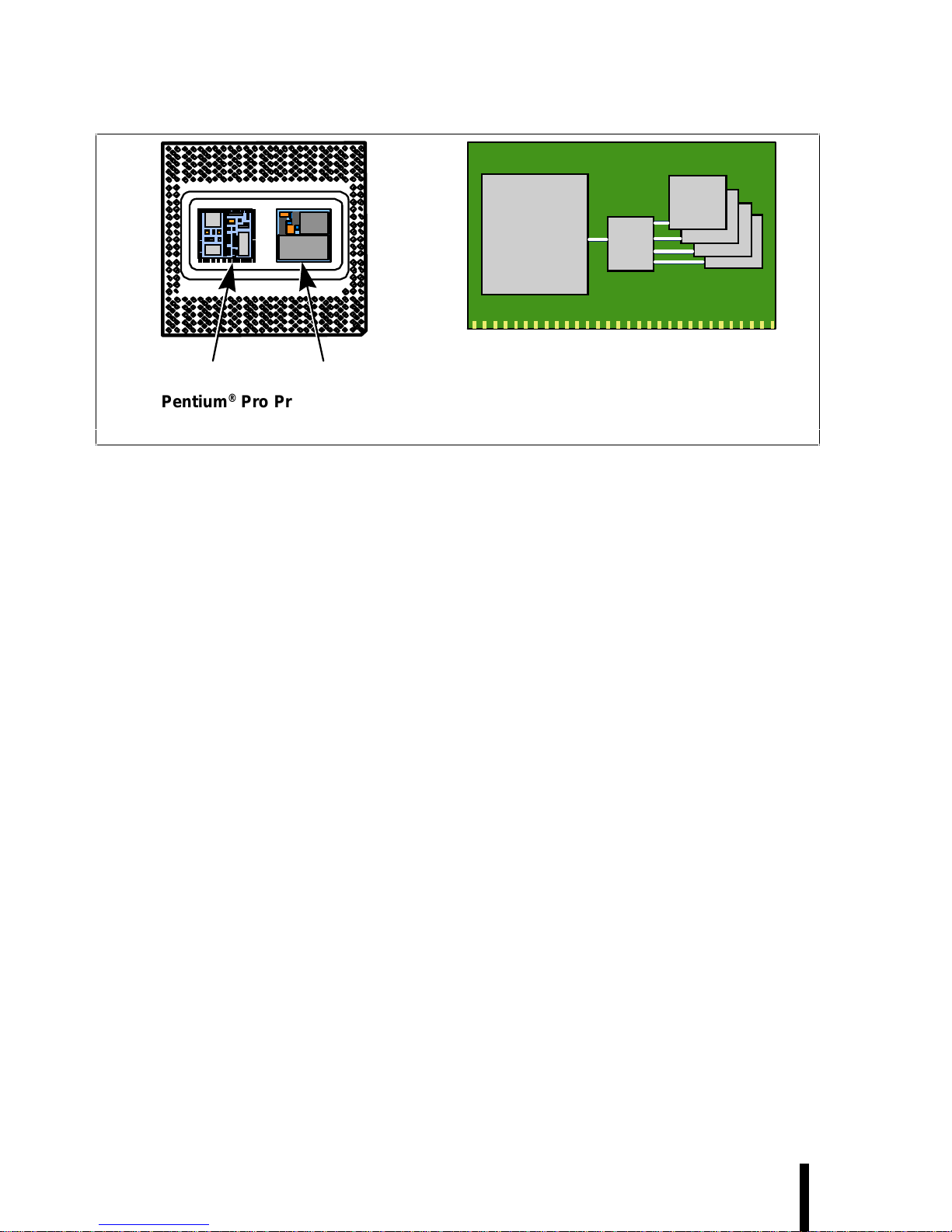
does not connect to the Pentium II processor system bus (see Figure 1-1). As with the
Pentium Pro processor, the Pentium II processor has a dedicated cache bus, thus maintaining
the dual independent bus architecture to deliver high bus bandwidth and high performance
(see Figure 1-1).
The Pentium II processor utilizes Single Edge Contact (S.E.C.) cartridge packaging
technology. The S.E.C. cartridge allows the L2 cache to remain tightly coupled to the
processor, while enabling use of high volume commercial SRAM components. The L2 cache
is performance optimized and tested at the package level. The S.E.C. cartridge utilizes
surface mount technology and a substrate with an edge finger connection. The S.E.C.
cartridge introduced on the Pentium II processor will also be used in future Slot 1 processors.
Page 14
COMPONENT INTRODUCTION E
1-2
Pentium II Processor
Substrate and Components
Processor Cor e
Processor
Core
Tag
L2
A
Pentium® Pro Processor
Dual Die Cavity Package
L2
Schemat ic onl y
000756c
Figure 1-1. Second Level Cache Implementations
The S.E.C. cartridge has the following features: a thermal plate, a cover and a substrate with
an edge finger connection. The thermal plate allows standardized heatsink attachment or
customized thermal solutions. The full enclosure also protects the surface mount components.
The edge finger connection maintains socketability for system configuration. The edge finger
connector is notated as ‘Slot 1 connector’ in this and other documentation.
1.2. TERMINOLOGY
In this document, a ‘#’ symbol after a signal name refers to an active low signal. This means
that a signal is in the active state (based on the name of the signal) when driven to a low
level. For example, when FLUSH# is low, a flush has been requested. When NMI is high, a
non-maskable interrupt has occurred. In the case of signals where the name does not imply an
active state but describes part of a binary sequence (such as address or data), the ‘#’ symbol
implies that the signal is inverted. For example, D[3:0] = ‘HLHL’ refers to a hex ‘A’, and
D#[3:0] = ‘LHLH’ also refers to a hex ‘A’ (H= High logic level, L= Low logic level).
The term “system bus” refers to the interface between the processor, system core logic (a.k.a.
the core logic components) and other bus agents. The system bus is a multiprocessing
interface to processors, memory and I/O. The term “cache bus” refers to the interface
between the processor and the L2 cache components (TagRAM and BSRAMs). The cache
bus does NOT connect to the system bus, and is not visible to other agents on the system bus.
When signal values are referenced in tables, a 0 indicates inactive and a 1 indicates active. 0
and 1 do not reflect voltage levels. A # after a signal name indicates active low. An entry of
1 for ADS# means that ADS# is active, with a low voltage level.
Page 15

E COMPONENT INTRODUCTION
1-3
1.2.1. S.E.C. Cartridge Terminology
The following terms are used often in this document and are explained here for clarification:
• Pentium
®
II Processor — The entire product including internal components, substrate,
thermal plate and cover.
• S.E.C. Cartridge — The new processor packaging technology is called a “Single Edge
Contact cartridge.”
• Processor Substrate —The structure on which the components are mounted inside the
S.E.C. cartridge (with or without components attached).
• Processor Core — The processor’s execution engine.
• Thermal Plate — The surface used to connect a heatsink or other thermal solutions to
the processor.
• Cover — The processor casing on the opposite side of the thermal plate.
• Latch Arms — A processor feature that can be utilized as a means for securing the
processor in the retention mechanism.
Additional terms referred to in this and other related documentation:
• Slot 1 — The connector that the S.E.C. cartridge plugs into, just as the Pentium
®
Pro
processor uses Socket 8.
• Retention Mechanism — A mechanical piece which holds the package in the Slot 1
connector.
• Heatsink Support — The support pieces that are mounted on the motherboard to
provide added support for heatsinks.
The L2 cache (TagRAM, BSRAM) dies keep standard industry names.
1.3. REFERENCES
The reader of this specification should also be familiar with material and concepts presented
in the following documents:
• AP-485, Intel Processor Identification with the CPUID Instruction (Order Number
241618)
• AP-585, Pentium
®
II Processor GTL+ Guidelines (Order Number 243330)
• AP-586, Pentium
®
II Processor Thermal Design Guidelines (Order Number 243331)
• AP-587, Pentium
®
II Processor Power Distribution Guidelines (Order Number 243332)
• AP-588, Mechanical and Assembly Technology for S.E.C. Cartridge Processors (Order
Number 243333)
• AP-589, Pentium
®
II Processor Electro-Magnetic Interference (Order Number 243334)
Page 16

COMPONENT INTRODUCTION E
1-4
• Pentium® II Processor Specification Update (Order Number 243337)
• Pentium
®
II Processor I/O Buffer Models, IBIS Format (Electronic Form)
• Intel Architecture Software Developer’s Manual
Volume I: Basic Architecture (Order Number 243190)
Volume II: Instruction Set Reference (Order Number 243191)
Volume III: System Programming Guide (Order Number 243192)
Page 17

E
Micro-Architecture
Overview
2
Page 18

Page 19
E
2-1
CHAPTER 2
MICRO-ARCHITECTURE OVERVIEW
The Pentium II processor uses the same dynamic execution micro-architecture as the other
members of P6 family of Intel Architecture processors. This three-way superscalar, pipelined
micro-architecture features a decoupled, multi-stage superpipeline, which trades less work
per pipestage for more stages. The Pentium II processor, for example, has twelve stages with
a pipestage time 33 percent less than the Pentium processor, which helps achieve a higher
clock rate on any given manufacturing process.
The approach used in the P6 family micro-architecture removes the constraint of linear
instruction sequencing between the traditional “fetch” and “execute” phases, and opens up a
wide instruction window using an instruction pool. This approach allows the “execute” phase
of the processor to have much more visibility into the program instruction stream so that
better scheduling may take place. It requires the instruction “fetch/decode” phase of the
processor to be much more efficient in terms of predicting program flow. Optimized
scheduling requires the fundamental “execute” phase to be replaced by decoupled
“dispatch/execute” and “retire” phases. This allows instructions to be started in any order but
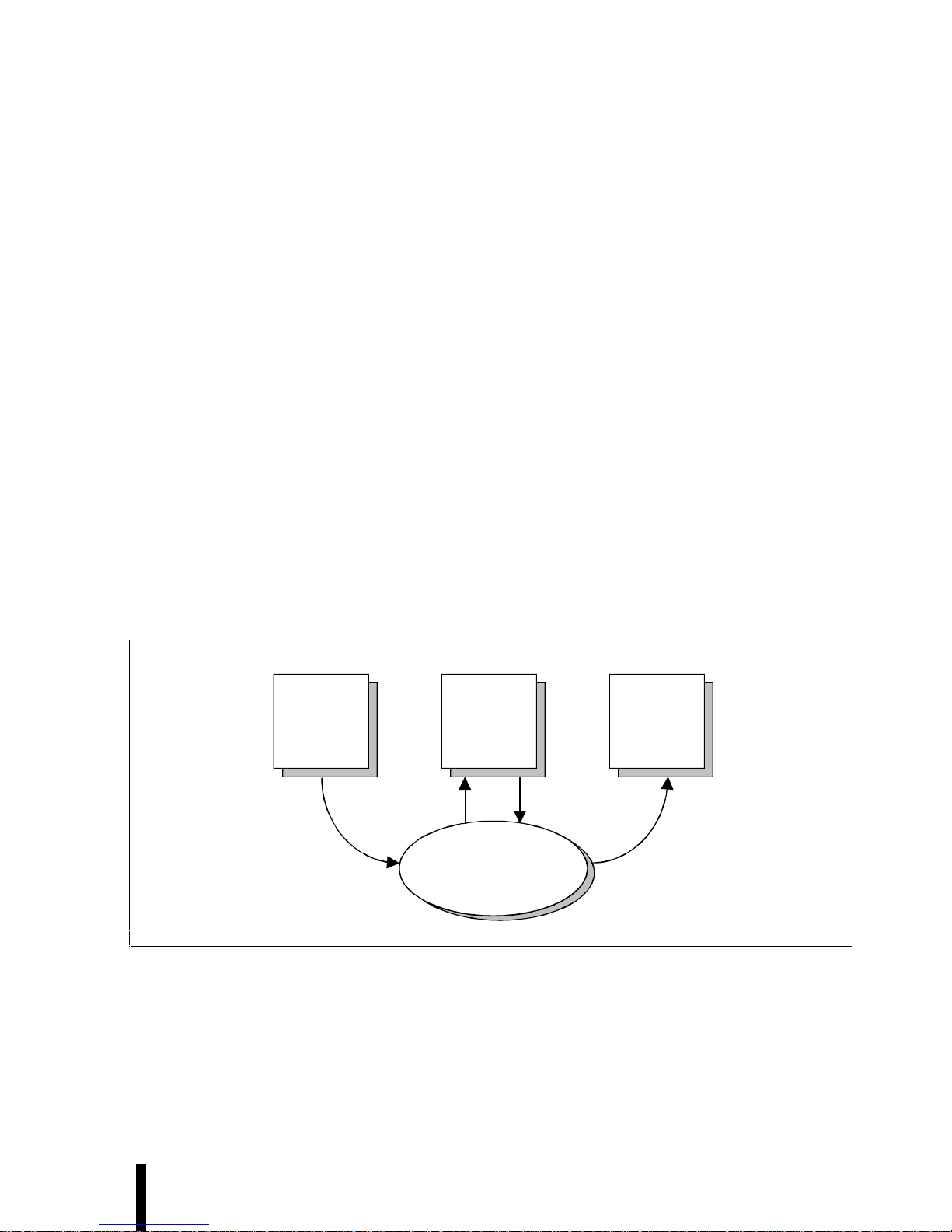
always be completed in the original program order. Processors in the P6 family may be
thought of as three independent engines coupled with an instruction pool as shown in
Figure 2-1.
Fetch/
Decode
Unit
Dispatch/
Execute
Unit
Retire
Unit
Instruction Pool
000925
Figure 2-1. Three Engines Communicating Using an Instruction Pool
Page 20

MICRO-ARCHITECTURE OVERVIEW E
2-2
2.1. FULL CORE UTILIZATION
The three independent-engine approach was taken to more fully utilize the processor core.
Consider the pseudo code fragment in Figure 2-2:
r1 <= mem [r0] /* Instruction 1 */
r2 <= r1 + r2 /* Instruction 2 */
r5 <= r5 + 1 /* Instruction 3 */
r6 <= r6 - r3 /* Instruction 4 */
000922
Figure 2-2. A Typical Pseudo Code Fragment
The first instruction in this example is a load of r1 that, at run time, causes a cache miss. A
traditional processor core must wait for its bus interface unit to read this data from main
memory and return it before moving on to instruction 2. This processor stalls while waiting
for this data and is thus being under-utilized.
To avoid this memory latency problem, a P6 family processor “looks-ahead” into the
instruction pool at subsequent instructions and does useful work rather than stalling. In the
example in Figure 2-2, instruction 2 is not executable since it depends upon the result of
instruction 1; however both instructions 3 and 4 have no prior dependencies and are therefore
executable. The processor executes instructions 3 and 4 out-of-order. The results of this outof-order execution can not be committed to permanent machine state (i.e., the programmervisible registers) immediately since the original program order must be maintained. The
results are instead stored back in the instruction pool awaiting in-order retirement. The core
executes instructions depending upon their readiness to execute, and not on their original
program order, and is therefore a true dataflow engine. This approach has the side effect that
instructions are typically executed out-of-order.
The cache miss on instruction 1 will take many internal clocks, so the core continues to look
ahead for other instructions that could be speculatively executed, and is typically looking 20
to 30 instructions in front of the instruction pointer. Within this 20 to 30 instruction window
there will be, on average, five branches that the fetch/decode unit must correctly predict if
the dispatch/execute unit is to do useful work. The sparse register set of an Intel Architecture
(IA) processor will create many false dependencies on registers so the dispatch/execute unit
will rename the Intel Architecture registers into a larger register set to enable additional
forward progress. The Retire Unit owns the programmer’s Intel Architecture register set and
results are only committed to permanent machine state in these registers when it removes
completed instructions from the pool in original program order.
Dynamic Execution technology can be summarized as optimally adjusting instruction
execution by predicting program flow, having the ability to speculatively execute instructions
in any order, and then analyzing the program’s dataflow graph to choose the best order to
execute the instructions.
Page 21
E MICRO-ARCHITECTURE OVERVIEW
2-3
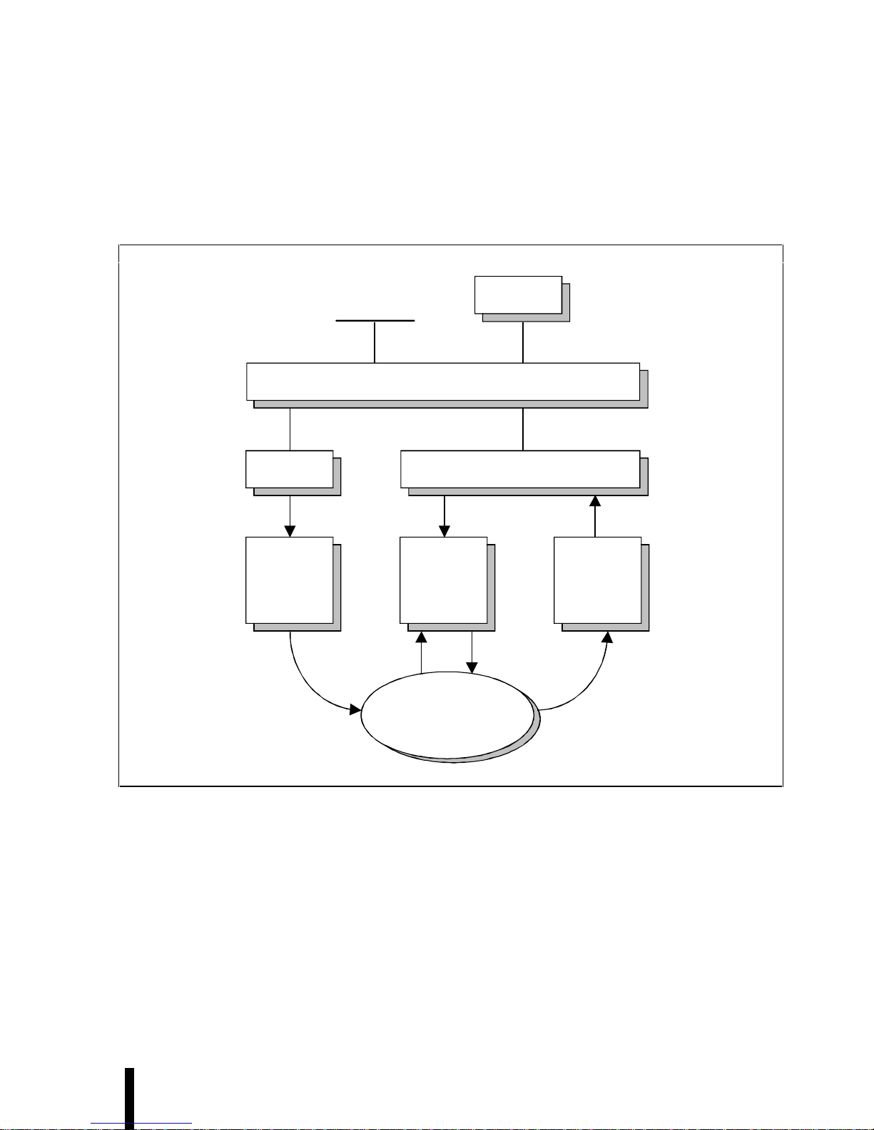
2.2. THE PENTIUM® II PROCESSOR PIPELINE
In order to get a closer look at how the P6 family micro-architecture implements Dynamic
Execution, Figure 2-3 shows a block diagram of the Pentium II processor with cache and
memory interfaces. The “Units” shown in Figure 2 represent stages of the Pentium II
processor pipeline.
Instru c tion Pool
L1 ICache L1 DCache
Bus Interface
Unit
L2 Cache
System Bus
Fetch Load
Store
Fetch/
Decode
Unit
Dispatch/
Execute
Unit
Retire
Unit
000926
Figure 2-3. The Three Core Engines Interface with Memory via Unified Caches
• The FETCH/DECODE unit: An in-order unit that takes as input the user program
instruction stream from the instruction cache, and decodes them into a series of
µoperations (µops) that represent the dataflow of that instruction stream. The pre-fetch is
speculative.
• The DISPATCH/EXECUTE unit: An out-of-order unit that accepts the dataflow stream,
schedules execution of the µops subject to data dependencies and resource availability
and temporarily stores the results of these speculative executions.
Page 22
MICRO-ARCHITECTURE OVERVIEW E
2-4
• The RETIRE unit: An in-order unit that knows how and when to commit (“retire”) the
temporary, speculative results to permanent architectural state.
• The BUS INTERFACE unit: A partially ordered unit responsible for connecting the
three internal units to the real world. The bus interface unit communicates directly with
the L2 (second level) cache supporting up to four concurrent cache accesses. The bus
interface unit also controls a transaction bus, with MESI snooping protocol, to system
memory.
2.2.1. The Fetch/Decode Unit
Figure 2-4 shows a more detailed view of the Fetch/Decode unit.
ICache
Next_IP
Microcode
Instruction
Sequencer
Instruction
Decoder
(x3)
From Bus Interface Unit
To Instruction
Pool (ReOrder Buffer)
Branch Target
Buffer
Register Alias
Table Allocate
000927
Figure 2-4. Inside the Fetch/Decode Unit
The L1 Instruction Cache is a local instruction cache. The Next_IP unit provides the L1
Instruction Cache index, based on inputs from the Branch Target Buffer (BTB), trap/interrupt
status, and branch-misprediction indications from the integer execution section.
The L1 Instruction Cache fetches the cache line corresponding to the index from the
Next_IP, and the next line, and presents 16 aligned bytes to the decoder. The prefetched
bytes are rotated so that they are justified for the instruction decoders (ID). The beginning
and end of the Intel Architecture instructions are marked.
Three parallel decoders accept this stream of marked bytes, and proceed to find and decode
the Intel Architecture instructions contained therein. The decoder converts the Intel
Architecture instructions into triadic µops (two logical sources, one logical destination per
Page 23
E MICRO-ARCHITECTURE OVERVIEW
2-5
µop). Most Intel Architecture instructions are converted directly into single µops, some
instructions are decoded into one-to-four µops and the complex instructions require
microcode (the box labeled Microcode Instruction Sequencer in Figure 2-4). This microcode
is just a set of preprogrammed sequences of normal µops. The µops are queued, and sent to
the Register Alias Table (RAT) unit, where the logical Intel Architecture-based register
references are converted into references to physical registers in P6 family processors physical
register references, and to the Allocator stage, which adds status information to the µops and
enters them into the instruction pool. The instruction pool is implemented as an array of
Content Addressable Memory called the ReOrder Buffer (ROB).
2.2.2. The Dispatch/Execute Unit
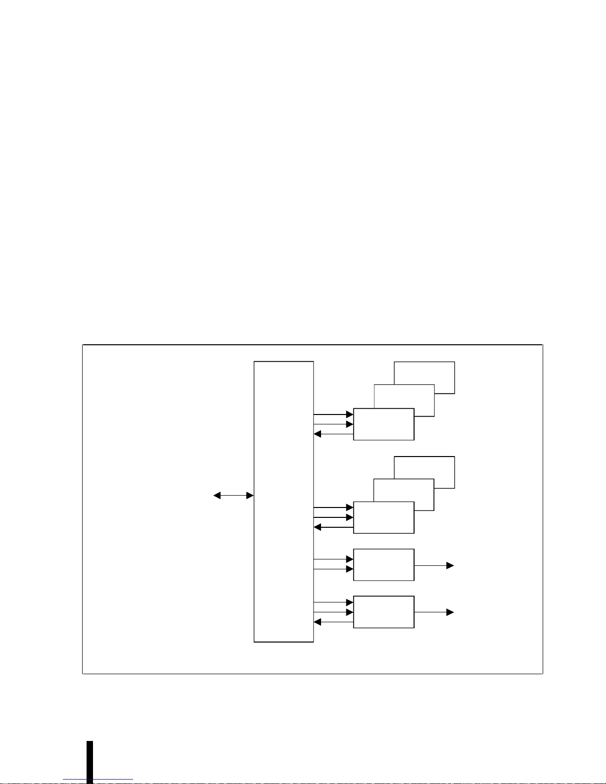
The Dispatch unit selects µops from the instruction pool depending upon their status. If the
status indicates that a µop has all of its operands then the dispatch unit checks to see if the
execution resource needed by that µop is also available. If both are true, the Reservation
Station removes that µop and sends it to the resource where it is executed. The results of the
µop are later returned to the pool. There are five ports on the Reservation Station, and the
multiple resources are accessed as shown in Figure 2-5.
MMX
Ex ecution Unit
MMX™
Ex ecution Unit
Floating-Point
Ex ecution Unit
000928
Reservatio
Station
Integer
Ex ecution Unit
Jump
Ex ecution Unit
Integer
Ex ecution Unit
Load
Unit
Store
Unit
Port 0
Port 1
Port 2
Port 3, 4
To/From
Instruction Pool
(ReOrder Buffer)
Stores
Loads
000928
Figure 2-5. Inside the Dispatch/Execute Unit
Page 24

MICRO-ARCHITECTURE OVERVIEW E
2-6
The Pentium II processor can schedule at a peak rate of 5 µops per clock, one to each
resource port, but a sustained rate of 3 µops per clock is more typical. The activity of this
scheduling process is the out-of-order process; µops are dispatched to the execution resources
strictly according to dataflow constraints and resource availability, without regard to the
original ordering of the program.
Note that the actual algorithm employed by this execution-scheduling process is vitally
important to performance. If only one µop per resource becomes data-ready per clock cycle,
then there is no choice. But if several are available, it must choose. The P6 family microarchitecture uses a pseudo FIFO scheduling algorithm favoring back-to-back µops.
Note that many of the µops are branches. The Branch Target Buffer will correctly predict
most of these branches but it can’t correctly predict them all. Consider a BTB that is
correctly predicting the backward branch at the bottom of a loop; eventually that loop is
going to terminate, and when it does, that branch will be mispredicted. Branch µops are
tagged (in the in-order pipeline) with their fall-through address and the destination that was
predicted for them. When the branch executes, what the branch actually did is compared
against what the prediction hardware said it would do. If those coincide, then the branch
eventually retires and the speculatively executed work between it and the next branch
instruction in the instruction pool is good.
But if they do not coincide, then the Jump Execution Unit (JEU) changes the status of all of
the µops behind the branch to remove them from the instruction pool. In that case the proper
branch destination is provided to the BTB which restarts the whole pipeline from the new
target address.
2.2.3. The Retire Unit
Figure 2-6 shows a more detailed view of the Retire Unit.
Page 25
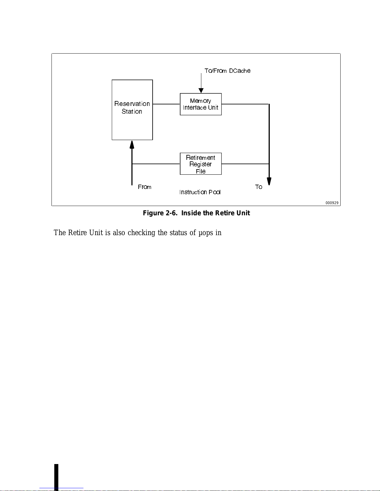
E MICRO-ARCHITECTURE OVERVIEW
2-7
Reservation
Station
Memory
Interface Unit
Retirement
Register
File
To/From DCache
From To
Instruction Pool
000929
Figure 2-6. Inside the Retire Unit
The Retire Unit is also checking the status of µops in the instruction pool. It is looking for
µops that have executed and can be removed from the pool. Once removed, the original
architectural target of the µops is written as per the original Intel Architecture instruction.
The Retire Unit must not only notice which µops are complete, it must also re-impose the
original program order on them. It must also do this in the face of interrupts, traps, faults,
breakpoints and mispredictions.
The Retire Unit must first read the instruction pool to find the potential candidates for
retirement and determine which of these candidates are next in the original program order.
Then it writes the results of this cycle’s retirements to the Retirement Register File (RRF).
The Retire Unit is capable of retiring 3 µops per clock.
2.2.4. The Bus Interface Unit
Figure 2-7 shows a more detailed view of the Bus Interface Unit.
Page 26
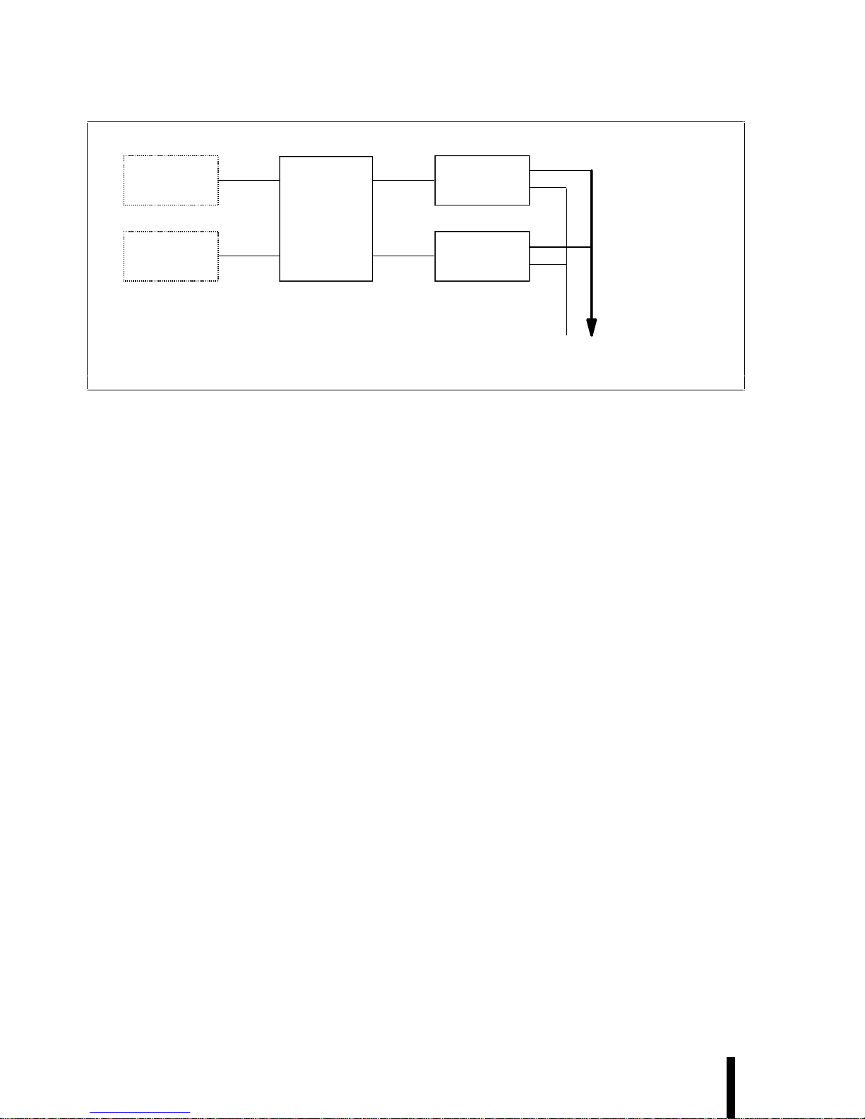
MICRO-ARCHITECTURE OVERVIEW E
2-8
Memory
I/F
Memory
Order Buffer
DCache
System
Memory
L2 Cache
From Address
Generation Unit
To/From
Instruction Pool
(ReOrder Buffer)
000930
Figure 2-7. Inside the Bus Interface Unit
There are two types of memory access: loads and stores. Loads only need to specify the
memory address to be accessed, the width of the data being retrieved, and the destination
register. Loads are encoded into a single µop.
Stores need to provide a memory address, a data width, and the data to be written. Stores
therefore require two µops, one to generate the address and one to generate the data. These
µops must later re-combine for the store to complete.
Stores are never performed speculatively since there is no transparent way to undo them.
Stores are also never re-ordered among themselves. A store is dispatched only when both the
address and the data are available and there are no older stores awaiting dispatch.
A study of the importance of memory access reordering concluded:
• Stores must be constrained from passing other stores, for only a small impact on
performance.
• Stores can be constrained from passing loads, for an inconsequential performance loss.
• Constraining loads from passing other loads or stores has a significant impact on
performance.
The Memory Order Buffer (MOB) allows loads to pass other loads and stores by acting like a
reservation station and re-order buffer. It holds suspended loads and stores and re-dispatches
them when a blocking condition (dependency or resource) disappears.
Page 27

E MICRO-ARCHITECTURE OVERVIEW
2-9
2.3. MMX™ TECHNOLOGY AND THE PENTIUM® II PROCESSOR
2.3.1. MMX™ Technology in the Pentium® II Processor Pipeline
Pentium II processors use a Dynamic Execution architecture that blend out-of-order and
speculative execution with hardware register renaming and branch prediction. These
processors feature an in-order issue pipeline, which breaks Intel386 processor macroinstructions up into simple, µoperations called µops (or uops), and an out-of-order,
superscalar processor core, which executes the µops. The out-of-order core of the processor
contains several pipelines to which integer, jump, floating-point, and memory execution units
are attached. Several different execution units may be clustered on the same pipeline: for
example, an integer address logic unit and the floating-point execution units (adder,
multiplier, and divider) share a pipeline. The data cache is pseudo-dual ported via
interleaving, with one port dedicated to loads and the other to stores. Most simple operations
(integer ALU, floating-point add, even floating-point multiply) can be pipelined with a
throughput of one or two operations per clock cycle. Floating-point divide is not pipelined.
Long latency operations can proceed in parallel with short latency operations.
The Pentium II pipeline is comprised of three parts: (1) the In-Order Issue Front-end, (2) the
Out-of-Order Core, and the (3) In-Order Retirement unit. Details about the In-Order Issue
Front-end follow below.
Since the dynamic execution processors execute instructions out of order, the most important
consideration in performance tuning is making sure enough µops are ready for execution.
Correct branch prediction and fast decoding are essential to getting the most performance out
of the In-Order Front-End. Branch prediction and the branch target buffer are discussed
below and are detailed in the MMX™ Technology Developer’s Guide at the Intel website:
http://developer.intel.com.
Page 28
MICRO-ARCHITECTURE OVERVIEW E
2-10
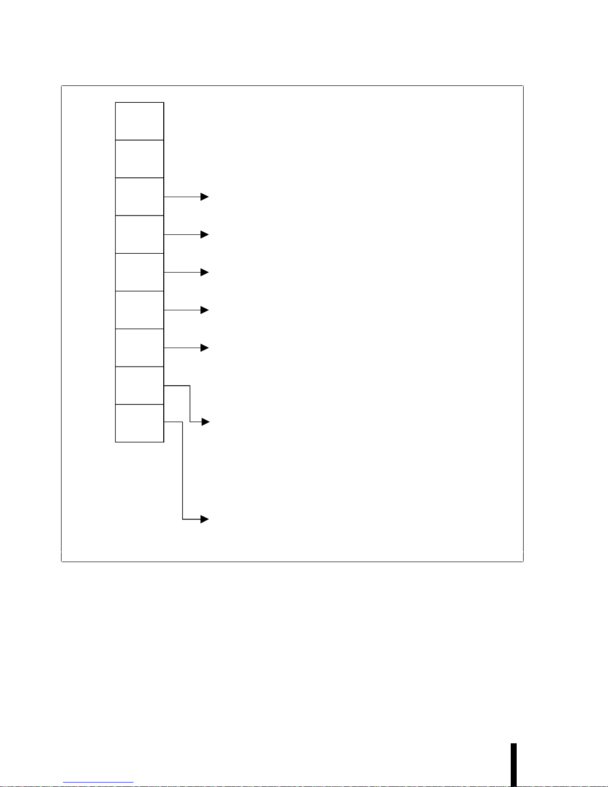
BTB0
BTB1
IFU0
IFU:
IFU1
IFU2
ID0
ID1
RAT
ROB
Rd
Instruction Cache Unit
IFU1: In this stage, 16-byte instruction packets are fetched.
The packets are aligned on 16-byte boundaries.
IFU2: Instruction Pre-decode: double buffered: 16-byte
packets aligned on any boundary.
ID0: Instruction Decode
ID1: Decode 1 stage: decoder limits
= at most 3 macro-instructions per cycle
= at most 6 µops (411) per cycle
= at most 3 µops per cycle exit the queue
= instructions ≤7 bytes in length
RAT: Register Allocati on
Decode IP relative branches
= at most one per cycle
= Branch inform at ion sent to BTB0 pipe stage
Rename = partial and flag stalls
Allocate resources = the pipeline stalls if the
ROB is full
ROB Re -ord e r Buf fer Rea d
= at most 2 completed physical registers reads
per cycle
001049
Figure 2-8. Out of Order Core and Retirement Pipeline
Page 29

E MICRO-ARCHITECTURE OVERVIEW
2-11
During every clock cycle, up to three Intel Architecture macro instructions can be decoded in
the ID1 pipestage. However, if the instructions are complex or are over seven bytes then the
decoder is limited to decoding fewer instructions.
The decoders can decode:
1. Up to three macro-instructions per clock cycle.
2. Up to six µops per clock cycle.
3. Macro-instructions up to seven bytes in length.
Pentium II processors have three decoders in the D1 pipestage. The first decoder is capable
of decoding one Intel Architecture macro-instruction of four or fewer µops in each clock
cycle. The other two decoders can each decode an Intel Architecture instruction of one µop in
each clock cycle. Instructions composed of more than four µops will take multiple cycles to
decode. When programming in assembly language, scheduling the instructions in a 4-1-1 µop
sequence increases the number of instructions that can be decoded each clock cycle. In
general:
• Simple instructions of the register-register form are only one µop.
• Load instructions are only one µop.
• Store instructions have two µops.
• Simple read-modify instructions are two µops.
• Simple instructions of the register-memory form have two to three µops.
• Simple read-modify write instructions are four µops.
• Complex instructions generally have more than four µops, therefore they will take
multiple cycles to decode.
For the purpose of counting µops, MMX technology instructions are simple instructions. See
Appendix D in AP-526, Optimizations for Intel’s 32-bit Processors (Order Number 242816)
for a table that specifies the number of µops for each instruction in the Intel Architecture
instruction set.
Once the µops are decoded, they will be issued from the In-Order Front-End into the
Reservation Station (RS), which is the beginning pipestage of the Out-of-Order core. In the
RS, the µops wait until their data operands are available. Once a µop has all data sources
available, it will be dispatched from the RS to an execution unit. If a µop enters the RS in a
data-ready state (that is, all data is available), then the µop will be immediately dispatched to
an appropriate execution unit, if one is available. In this case, the µop will spend very few
clock cycles in the RS. All of the execution units are clustered on ports coming out of the RS.
Once the µop has been executed it returns to the ROB, and waits for retirement.
In this pipestage, all data values are written back to memory and all µops are retired in-order,
three at a time. The figure below provides details about the Out-of-Order core and the InOrder retirement pipestages.
Page 30
MICRO-ARCHITECTURE OVERVIEW E
2-12
Port 0
Port 1
ROB
wb
RRF
ROBrdROB
rd
RS
Port 2
Port 3
Port 4
Additional information regarding
each pipeline is in the following
table.
Execution pipelines coming out of the RS are
multiple pipelines grouped into five clusters.
Re-order Buffer
Writeback (ROB wb)
Retirement (RRF): At most,
three µops are retired per
cycle. Taken branches must
retire in the first slot.
Reservation station (RS): A µop can remain in the RS for
many cycles or simply move past to an execution unit.
On average, a µop will remain in the RS for three cycles
or pipestages.
001050
Figure 2-9. Out-of-Order Core and Retirement Pipeline
Page 31

E MICRO-ARCHITECTURE OVERVIEW
2-13
Table 2-1. Pentium® II Processor Execution Unit Pipelines
Port Execution Unit Latency/Throughput Notes
0 Integer ALU Unit Latency 1, Throughput 1/cycle
0 LEA instructions Latency 1, Throughput 1/cycle
0 Shift Instructions Latency 1, Throughput 1/cycle
0 Integer Multiplication instruction Latency 4, Throughput 1/cycle
0 Floating-Point Unit Latency 3, Throughput 1/cycle
0 FADD instruction
FMUL
FDIV Unit
Latency 5, Throughput 1-2/cycle
Latency long and data dependant, Throughput
non-pipelined
1,2
0 MMX™ Technology ALU Unit Latency 1, Throughput 1/cycle
0 MMX Technology Multiplier
Unit
Latency 3, Throughput 1/cycle
1 Integer ALU Unit Latency 1, Throughput 1/cycle
1 MMX Technology ALU Unit Latency 1, Throughput 1/cycle
1 MMX Technology Shifter Unit Latency 1, Throughput 1/cycle
2 Load Unit Latency 3 on a cache hit, Throughput 1/cycle
(3)
4
3 Store Address Unit Latency 3 (N/A)
Throughput 1/cycle
(3)
3
4 Store Data Unit Latency 1 (N/A)
Throughput 1/cycle
NOTES:
1. The FMUL unit cannot accept a second FMUL within the cycle after it has accepted the first. This is NOT
the same as only being able to do FMULs on even clock cycles.
2. FMUL is pipelined one every two clock cycles. One way of thinking about this is to imagine that a P6family processor has only a 32x32->32 multiply pipelined.
3. Store latency is not all that important from a dataflow perspective. The latency that matters is with respect
to determining when they can retire and be completed. They also have a different latency with respect to
load forwarding. For example, if the store address and store data of a particular address, for example
100, dispatch in clock cycle 10, a load (of the same size and shape) to the same address 100 can
dispatch in the same clock cycle 10 and not be stalled.
4. A load and store to the same address can dispatch in the same clock cycle.
2.3.2. Caches
The on-chip cache subsystem of processors with MMX technology consists of two 16K fourway set associative caches with a cache line length of 32 bytes. The caches employ a write-
Page 32

MICRO-ARCHITECTURE OVERVIEW E
2-14
back mechanism and a pseudo-LRU replacement algorithm. The data cache consists of eight
banks interleaved on four-byte boundaries.
On the Pentium II processors, the data cache can be accessed simultaneously by a load
instruction and a store instruction, as long as the references are to different cache banks. On
Pentium II processors the minimum delay is ten internal clock cycles.
2.4. WRITE BUFFERS
Processors with MMX technology have four write buffers (versus two in Pentium processors
without MMX technology). Additionally, the write buffers can be used by either pipe (versus
one corresponding to each pipe in Pentium processors without MMX technology).
Performance of critical loops can be improved by scheduling the writes to memory; when
you expect to see write misses, you should schedule the write instructions in groups no larger
than four, then schedule other instructions before scheduling further write instructions.
2.5. ADDITIONAL INFORMATION
For more information on how to program with MMX Technology, see the MMX™
Technology Developer’s Guide on the Intel web site at http://developer.intel.com.
2.6. ARCHITECTURE SUMMARY
Dynamic Execution is the combination of improved branch prediction, speculative execution
and data flow analysis that enable P6 family processors to deliver superior performance. The
addition of MMX technology makes the Pentium II processor the fastest processor in the
Intel family of processors.
Page 33

E
System Bus Overview
3
Page 34

Page 35

E
3-1
CHAPTER 3
SYSTEM BUS OVERVIEW
This chapter provides an overview of the Pentium II processor system bus, bus transactions,
and bus signals. The Pentium II processor system bus is based on the P6 Family system bus
architecture, which is also implemented in the Pentium Pro processor. The Pentium II
processor also supports two other synchronous busses (the APIC and the TAP bus), PC
compatibility signals, and several implementation specific signals. For a functional
overview of bus signals, see Appendix A, Signals Reference.
3.1. SIGNALING ON THE PENTIUM® II PROCESSOR SYSTEM
BUS
The Pentium II processor system bus supports a synchronous latched protocol. On the rising
edge of the bus clock, all agents on the system bus are required to drive their active outputs
and sample required inputs. No additional logic is located in the output and input paths
between the buffer and the latch stage, thus keeping setup and hold times constant for all bus
signals following the latched protocol. The System bus requires that every input be sampled
during a valid sampling window on a rising clock edge and its effect be driven out no sooner
than the next rising clock edge. This approach allows one full clock for inter-component
communication and at least one full clock at the receiver to compute a response.
Figure 3-1 illustrates the latched bus protocol as it appears on the bus. In subsequent
descriptions, the protocol is described as “B# is asserted in the clock after A# is observed
active”, or “B# is asserted two clocks after A# is asserted”. Note that A# is asserted in T1,
but not observed active until T2. The receiving agent uses T2 to determine its response and
asserts B# in T3. Other agents observe B# active in T4.
BCLK
A#
B#
12345
Full clock allowed
for logic delays
Full clock allowed for
signal propagation
Assert # La tch A# Assert B# Latch B#
000936
Figure 3-1. Latched Bus Protocol
Page 36

SYSTEM BUS OVERVIEW E
3-2
The square and circle symbols are used in the timing diagrams to indicate the clock in which
particular signals of interest are driven and sampled. The square indicates that a signal is
driven (asserted, initiated) in that clock. The circle indicates that a signal is sampled
(observed, latched) in that clock.
Signals that are driven in the same clock by multiple System bus agents exhibit a “wired-OR
glitch” on the electrical-low-to-electrical-high transition. To account for this situation, these
signal state transitions are specified to have two clocks of settling time when deasserted
before they can be safely observed. The bus signals that must meet this criteria are: BINIT#,
HIT#, HITM#, BNR#, AERR#, BERR#.
3.2. SIGNAL OVERVIEW
This section describes the function of the System bus signals. In this section, the signals are
grouped according to function.
3.2.1. Execution Control Signals
Table 3-1 lists the execution control signals, which control the execution and initialization of
the processor.
Table 3-1. Execution Control Signals
Pin/Signal Name Pin/Signal Mnemonic
Bus Clock BCLK
Initialization INIT#, RESET#
Flush FLUSH#
Stop Clock STPCLK#
Sleep SLP#
Interprocessor Communication and Interrupts PICCLK, PICD[1:0]#, LINT[1:0]
The BCLK (Bus Clock) input signal is the System bus clock. All agents drive their outputs
and latch their inputs on the BCLK rising edge. Each processor in the P6 family derives its
internal clock from BCLK by multiplying the BCLK frequency by a multiplier determined at
configuration. See Chapter 5, Configuration, for possible clock configuration frequencies.
The RESET# input signal resets all System bus agents to known states and invalidates their
internal caches. Modified or dirty cache lines are NOT written back. After RESET# is
deasserted, each processor begins execution at the power on reset vector defined during
configuration.
Page 37

E SYSTEM BUS OVERVIEW
3-3
The INIT# input signal resets all processors without affecting their internal (L1 or L2)
caches, floating-point registers, or their Machine Check Architecture registers (MCi–CTL).
Each processor begins execution at the address vector as defined during power on
configuration. INIT# has another meaning on RESET#’s active to inactive transition: if
INIT# is sampled active on RESET#’s active to inactive transition, then the processor
executes its built-in self test (BIST).
If the FLUSH# input signal is asserted, the processor writes back all internal cache lines in
the Modified state (L1 and L2 caches) and invalidates all internal cache lines (L1 and L2
caches). The flush operation puts all internal cache lines in the Invalid state. All lines are
written back and invalidated. The FLUSH# signal has a different meaning when it is sampled
asserted on the active to inactive transition of RESET#. If FLUSH# is sampled asserted on
the active to inactive transition of RESET#, then the processor tristates all of its outputs. This
function is used during board testing.
The Pentium II processor supplies a STPCLK# pin to enable the processor to enter a low
power state. When STPCLK# is asserted, the processor puts itself into the Stop-Grant state.
The processor continues to snoop bus transactions while in Stop-Grant state. When
STPCLK# is deasserted, the processor restarts its internal clock to all units and resumes
execution. The assertion of STPCLK# has no effect on the bus clock.
The SLP# signal is the Sleep signal. When asserted in Stop-Grant state, the processor enters a
new low power state, the Sleep state. During Sleep state, the processor stops providing
internal clock signals to all units, only leaves PLL still running. Snooping during the Sleep
state is not supported.
The PICCLK and PICD[1:0]# signals support the Advanced Programmable Interrupt
Controller (APIC) interface. The PICCLK signal is a clock input for the processor’s APIC
bus clock. The PICD[1:0]# signals are used for bi-directional serial message passing on the
APIC bus.
LINT[1:0] are local interrupt signals, also defined by the APIC interface. In APIC disabled
mode, LINT0 defaults to INTR, a maskable interrupt request signal. LINT1 defaults to NMI,
a non-maskable interrupt. Both signals are asynchronous inputs. In the APIC enable mode,
LINT0 and LINT1 are defined with the local vector table.
LINT[1:0] are also used along with the A20M# and IGNNE# signals to determine the
multiplier for the internal clock frequency as described in Chapter 5, Configuration.
3.2.2. Arbitration Signals
The arbitration signal group (see Table 3-2) is used to arbitrate for the bus.
The Pentium II processor permits up to three agents to simultaneously arbitrate for the
system bus with one to two symmetric agents (on BREQ[1:0]#) and one priority agent (on
BPRI#). P6 family processors arbitrate as symmetric agents. The priority agent normally
arbitrates on behalf of the I/O subsystem (I/O agents) and memory subsystem (memory
agents). Owning the bus is a necessary condition for initiating a bus transaction.
Page 38

SYSTEM BUS OVERVIEW E
3-4
Table 3-2. Arbitration Signals
Pin/Signal Name Pin Mnemonic Signal Mnemonic
Symmetric Agent Bus Request BR[1:0]# BREQ[1:0]#
Priority Agent Bus Request BPRI# BPRI#
Block Next Request BNR# BNR#
Lock LOCK# LOCK#
The symmetric agents arbitrate for the bus based on a round-robin rotating priority scheme.
The arbitration is fair and symmetric. After reset, agent 0 has the highest priority followed by
agent 1. All bus agents track the current bus owner. A symmetric agent requests the bus by
asserting its BREQn# signal. Based on the values sampled on BREQ[1:0]#, and the last
symmetric bus owner, all agents simultaneously determine the next symmetric bus owner.
The priority agent asks for the bus by asserting BPRI#. The assertion of BPRI# temporarily
overrides, but does not otherwise alter the symmetric arbitration scheme. When BPRI# is
sampled active, no symmetric agent issues another unlocked bus transaction until BPRI# is
sampled inactive. The priority agent is always the next bus owner.
BNR# can be asserted by any bus agent to block further transactions from being issued to the
bus. It is typically asserted when system resources (such as address and/or data buffers) are
about to become temporarily busy or filled and cannot accommodate another transaction.
After bus initialization, BNR# can be asserted to delay the first bus transaction until all bus
agents are initialized.
The assertion of the LOCK# signal indicates that the bus agent is executing an atomic
sequence of bus transactions that must not be interrupted. A locked operation cannot be
interrupted by another transaction regardless of the assertion of BREQ[1:0]# or BPRI#.
LOCK# can be used to implement memory-based semaphores. LOCK# is asserted from the
start of the first transaction through the end of the last transaction. The LOCK# signal is
always deasserted between two sequences of locked transactions on the System bus.
Page 39

E SYSTEM BUS OVERVIEW
3-5
3.2.3. Request Signals
The request signals (see Table 3-3) initiate a transaction.
Table 3-3. Request Signals
Pin Name Pin Mnemonic Signal Name
Signal Mnemonic
Address Strobe ADS# Address Strobe
ADS#
Request Command REQ[4:0]# Request
REQ[4:0]#
Address A[35:3]# Address
A[35:3]#
Address Parity AP[1:0]# Address Parity
AP[1:0]#
Request Parity RP# Request Parity
RP#
The assertion of ADS# defines the beginning of the transition. The REQ[4:0]#, A[35:3]#,
RP# and AP[1:0]# signals are valid in the clock that ADS# is asserted.
In the clock that ADS# is asserted, the A[35:3]# signals provide a 36-bit, active-low address
as part of the request. The Pentium II processor physical address space is 2
36
bytes or 64gigabits (64 GByte). Address bits 2, 1, and 0 are mapped into byte enable signals for 1 to 8
byte transfers.
The address signals are protected by the AP[1:0]# pins. AP1# covers A[35:24]#, AP0# covers
A[23:3]#. AP[1:0]# must be valid for two clocks beginning when ADS# is asserted. A parity
signal on the system bus is correct if there are an even number of electrically low signals in
the set consisting of the covered signals plus the parity signal. Parity is computed using
voltage levels, regardless of whether the covered signals are active high or active low.
The Request Parity pin RP# covers the request pins REQ[4:0]# and the address strobe, ADS#.
3.2.4. Snoop Signals
The snoop signal group (see Table 3-4) provides snoop result information to the System bus
agents.
Table 3-4. Snoop Signals
Type Signal Names
Keeping a Non-Modified Cache Line HIT#
Hit to a Modified Cache Line HITM#
Defer Transaction Completion DEFER#
Page 40

SYSTEM BUS OVERVIEW E
3-6
On observing a transaction, HIT# and HITM# are used to indicate that the line is valid or
invalid in the snooping agent, whether the line is in the modified (dirty) state in the caching
agent, or whether the transaction needs to be extended. The HIT# and HITM# signals are
used to maintain cache coherency at the system level.
If the memory agent observes HITM# active, it relinquishes responsibility for the data return
and becomes a target for the implicit cache line writeback. The memory agent must merge
the cache line being written back with any write data and update memory. The memory agent
must also provide the implicit writeback response for the transaction.
If HIT# and HITM# are sampled asserted together, it means that a caching agent is not ready
to indicate snoop status, and it needs to extend the transaction.
DEFER# is deasserted to indicate that the transaction can be guaranteed in-order completion.
An agent asserting DEFER# ensures proper removal of the transaction from the In-order
Queue by generating the appropriate response.
3.2.5. Response Signals
The response signal group (see Table 3-5) provides response information to the requesting
agent.
Table 3-5. Response Signals
Type Signal Names
Response Status RS[2:0]#
Response Parity RSP#
Target Ready (for writes) TRDY#
Requests initiated in the Request Phase enter the In-order Queue, which is maintained by
every agent. The response agent is the agent responsible for completing the transaction at the
top of the In-order Queue. The response agent is the agent addressed by the transaction.
For write transactions, TRDY# is asserted by the response agent to indicate that it is ready to
accept write or writeback data. For write transactions with an implicit writeback, TRDY# is
asserted twice, first for the write data transfer and then again for the implicit writeback data
transfer.
The RSP# signal provides parity for RS[2:0]#. A parity signal on the System bus is correct if
there are an even number of low signals in the set consisting of the covered signals plus the
parity signal. Parity is computed using voltage levels, regardless of whether the covered
signals are active high or active low.
Page 41

E SYSTEM BUS OVERVIEW
3-7
3.2.6. Data Response Signals
The data response signals (see Table 3-6) control the transfer of data on the bus and provide
the data path
Table 3-6. Data Phase Signals
Type Signal Names
Data Ready DRDY#
Data Bus Busy DBSY#
Data D[63:0]#
Data ECC Protection DEP[7:0]#
DRDY# indicates that valid data is on the bus and must be latched. The data bus owner
asserts DRDY# for each clock in which valid data is to be transferred. DRDY# can be
deasserted to insert wait states in the Data transfer.
DBSY# is used to hold the bus before the first DRDY# and between DRDY# assertions for a
multiple clock data transfer. DBSY# need not be asserted for single clock data transfers if no
wait states are needed.
The D[63:0]# signals provide a 64-bit data path between bus agents.
The DEP[7:0]# signals provide optional ECC (error correcting code) covering D[63:0]#. As
described in Chapter 5, Configuration, the Pentium II data bus can be configured with either
no checking or ECC. If ECC is enabled, then DEP[7:0]# provides valid ECC for the entire
data bus on each data clock, regardless of which bytes are enabled. The error correcting code
can correct single bit errors and detect double bit errors.
3.2.7. Error Signals
Table 3-7 lists the error signals on the system bus.
Table 3-7. Error Signals
Type Signal Names
Bus Initialization BINIT#
Bus Error BERR#
Internal Error IERR#
FRC Error FRCERR
Address Parity Error AERR#
Page 42

SYSTEM BUS OVERVIEW E
3-8
AERR#, can be enabled or disabled as part of the power on configuration (see Chapter 5,
Configuration). If AERR# is disabled for all system bus agents, request and address parity
errors are ignored and no action is taken by bus agents. If AERR# is enabled for at least one
bus agent, the agents observing the start of a transaction check the Address Parity signals
(AP[1:0]#) and the RP# parity signal and assert AERR# appropriately if an address parity
error is detected.
P6 family processors support two modes of response when the AERR# signal is enabled. This
may be configured at power-up with “AERR# observation” mode. AERR# observation
configuration must be consistent between all bus agents. If AERR# observation is disabled,
AERR# is ignored and no action is taken by the bus agents. If AERR# observation is enabled
and AERR# is sampled asserted, the transaction is canceled. In addition, the requesting agent
may retry the transaction at a later time up to its retry limit, after which the error becomes a
hard error as determined by the initiating processor.
If a transaction is canceled by AERR# assertion, then the transaction is aborted. Snoop
results are ignored if they cannot be canceled in time. All agents reset their rotating ID for
bus arbitration to the state at reset (such that bus agent 0 has highest priority).
BINIT# is used to signal any bus condition that prevents reliable future operation of the bus.
Like the AERR# pin, the BINIT# driver can be enabled or disabled as part of the power-on
configuration (see Chapter 5, Configuration). If the BINIT# driver is disabled, BINIT# is
never asserted and no action is taken on bus errors.
Regardless of whether the BINIT# driver is enabled, the Pentium II processor supports two
modes of operation that may be configured at power on. These are the BINIT# observation
and driving modes. If BINIT# observation is disabled, BINIT# is ignored and no action is
taken by the processor even if BINIT# is sampled asserted. If BINIT# observation is enabled
and BINIT# is sampled asserted, all bus state machines are reset. All agents reset their
rotating ID for bus arbitration, and internal state information is lost. L1 and L2 cache
contents are not affected.
The BERR# pin is used to signal any error condition caused by a bus transaction that will not
impact the reliable operation of the bus protocol (for example, memory data error, nonmodified snoop error). A bus error that causes the assertion of BERR# can be detected by the
processor, or by another bus agent. The BERR# driver can be enabled or disabled at poweron reset. If the BERR# driver is disabled, BERR# is never asserted. If the BERR# driver is
enabled, the processor may assert BERR#.
A machine check exception may or may not be taken for each assertion of BERR# as
configured at power on. A processor will always disable the machine check exception by
default.
If a processor detects an internal error unrelated to bus operation, it asserts IERR#. For
example, a parity error in an L1 or L2 cache causes a Pentium Pro processor to assert IERR#.
A machine check exception may be taken instead of assertion of IERR# as configured with
software.
Two processor agents in the P6 family may be configured as an FRC (functional redundancy
checking) pair. In this configuration, one processor acts as the master and the other acts as a
Page 43

E SYSTEM BUS OVERVIEW
3-9
checker, and the pair operates as a single processor. If the checker agent detects a mismatch
between its internally sampled outputs and the master processor’s outputs, the checker asserts
FRCERR. FRCERR observation can be enabled at the master processor with software. The
master enters machine check on an FRCERR provided that Machine Check Execution is
enabled.
The FRCERR signal is also toggled during an FRC checker agent’s reset action. FRCERR is
asserted one clock after RESET# transitions from its active to inactive state. If the checker
processor executes its built-in self test (BIST), then FRCERR is asserted throughout that test.
After BIST completes, the checker processor desserts FRCERR only if BIST succeeded but
continues to assert FRCERR if BIST failed. This feature allows the failure to be externally
observed. If the checker processor does not execute its BIST, then it keeps FRCERR asserted
for less than 20 clocks and then deasserts it.
3.2.8. Compatibility Signals
The compatibility signals group (see Table 3-8) contains signals defined for compatibility
within the Intel Architecture processor family.
Table 3-8. PC Compatibility Signals
Type Signal Names
Floating-Point Error FERR#
Ignore Numeric Error IGNNE#
Address 20 Mask A20M#
System Management Interrupt SMI#
A P6 family agent asserts FERR# when it detects an unmasked floating-point error. FERR# is
included for compatibility with systems using DOS-type floating-point error reporting.
If the IGNNE# input signal is asserted, the processor ignores a numeric error and continues to
execute non-control floating-point instructions. If the IGNNE# input signal is deasserted, the
processor freezes on a non-control floating-point instruction if a previous instruction caused
an error.
If the A20M# input signal is asserted, the processor masks physical address bit 20 (A20#)
before looking up a line in any internal cache and before driving a memory read/write
transaction on the bus. Asserting A20M# emulates the 8086 processor’s address wraparound
at the one Mbyte boundary. A20M# must only be asserted when the processor is in real
mode. A20M# is not used to mask external snoop addresses.
The IGNNE# and A20M# signals are valid at all times. These signals are normally not
guaranteed recognition at specific boundaries.
Page 44

SYSTEM BUS OVERVIEW E
3-10
The A20M# and IGNNE# signals have different meanings during a reset. A20M# and
IGNNE# are sampled on the active to inactive transition of RESET# to determine the
multiplier for the internal clock frequency, as described in Chapter 5, Configuration.
System Management Interrupt is asserted asynchronously by system logic. On accepting a
System Management Interrupt, the processor saves the current state and enters SMM mode. It
issues an SMI Acknowledge Bus transaction and then begins program execution from the
SMM handler.
3.2.9. Diagnostic Signals
The BP[3:2]# signals are the System Support group Breakpoint signals. They are outputs
from the processor that indicate the status of breakpoints.
The BPM[1:0]# signals are more System Support group breakpoint and performance monitor
signals. They are outputs from the processor that indicate the status of breakpoints and
programmable counters used for monitoring performance.
The diagnostic signals group shown in Table 3-9 provides signals for probing the processor,
monitoring processor performance, and implementing an IEEE 1149.1 boundary scan.
Table 3-9. Diagnostic Support Signals
Type Signal Names
Breakpoint Signals BP[3:2]#
Performance Monitor BPM[1:0]#
Boundary Scan/Test Access TCK, TDI, TDO, TMS, TRST#
Page 45

E
Data Integrity
4
Page 46

Page 47

E
4-1
CHAPTER 4
DATA INTEGRITY
The P6 family and the Pentium II processor system bus incorporate several advanced data
integrity features to improve error detection, retry, and correction. The Pentium II processor
system bus includes parity protection for address/request signals, parity or protocol protection
on most control signals, and ECC protection for data signals. The P6 family provides the
maximum possible level of error detection by incorporating functional redundancy checking
(FRC) support.
The P6 family data integrity features can be categorized as follows:
• Processor internal error detection
• Level 2 (L2) cache and Core-to-L2 cache-interface error detection and limited recovery
• Pentium
®
II processor system bus error detection and limited recovery
• Pentium II processor system bus FRC support
In addition, the P6 family extends the Pentium II processor’s data integrity features in several
ways to form a machine check architecture. Several model specific registers are defined for
reporting error status. Hardware corrected errors are reported to registers associated with the
unit reporting the error. Unrecoverable errors cause the INT 18 machine check exception, as
in the Pentium Pro processor.
If machine check is disabled, or an error occurs in a Pentium II processor system bus agent
without the machine check architecture, the Pentium II processor system bus defines a bus
error reporting mechanism. The central agent can then be configured to invoke the exception
handler via an interrupt (NMI) or soft reset (INIT#).
The terminology used in this chapter is listed below:
• Machine Check Architecture (MCA)
• Machine Check Exception (MCE)
• Machine Check Enable bit (CR4.MCE)
• Machine Check In Progress (MCIP)
For more information on Machine Check Architecture, see the Intel Architecture Software
Developer’s Manual, Volume 3: System Programming Guide.
4.1. ERROR CLASSIFICATION
The Pentium II processor system bus architecture uses the following error classification. An
implementation may always choose to report an error in a more severe category to simplify
its logic.
Page 48

DATA INTEGRITY E
4-2
• Recoverable Error (RE): The error can be corrected by a retry or by using ECC
information. The error is logged in the MCA hardware.
• Unrecoverable Error (UE): The error cannot be corrected, but it only affects one agent.
The memory interface logic and bus pipeline are intact, and can be used to report the
error via an exception handler.
• Fatal Error (FE): The error cannot be corrected and may affect more than one agent.
The memory interface logic and bus pipeline integrity may have been violated, and
cannot be reliably used to report the error via an exception handler. A bus pipeline reset
is required of all bus agents before operation can continue. An exception handler may
then proceed.
4.2. PENTIUM® II PROCESSOR SYSTEM BUS DATA INTEGRITY
ARCHITECTURE
The Pentium II processor system bus’ major address and data paths are protected by ten
check bits, providing parity or ECC. Eight ECC bits protect the data bus. Single-bit data ECC
errors are automatically corrected. A two-bit parity code protects the address bus. Any
address parity error on the address bus when the request is issued can be optionally retried to
attempt a correction.
Two control signal groups are explicitly protected by individual parity bits: RP# and RSP#.
Errors on most remaining bus signals can be detected indirectly due to a well-defined bus
protocol specification that enables detection of protocol violation errors. Errors on a few bus
signals cannot be detected without the use of FRC mode.
An agent is not required to support all data integrity features, as each feature is individually
enabled through the power-on configuration register. See Chapter 5, Configuration.
4.2.1. Bus Signals Protected Directly
Most Pentium II processor system bus signals are protected by parity or ECC. Table 4-1
shows which signals protect which signals.
Table 4-1. Direct Bus Signal Protection
Signal Protects
RP# ADS#,REQ[4:0]#
AP[0]# A[23:3]#
AP[1]# A[35:24]#
RSP# RS[2:0]#
DEP[7:0]# D[63:0]#
Page 49

E DATA INTEGRITY
4-3
• Address/Request Bus Signals. A parity error detected on AP[1:0]# or RP# is reported or
retried based on the following options defined by the power-on configuration:
— AERR# driver disabled.
The agent detecting the parity error ignores it and continues normal operation. This
option is normally used in power-on system initialization and system diagnostics.
— AERR# driver enabled, AERR# observation disabled.
The agent detecting the parity error asserts the AERR# signal. This signal can be
trapped by the central agent and be driven back to one of the processors as NMI.
— AERR# driver enabled, AERR# observation enabled.
The agent detecting the parity error asserts the AERR# signal. All bus agents must
observe AERR# and on the next clock reset bus arbiters and abort the erroneous
transaction by removing the transaction from the In-Order Queue and canceling a ll
remaining phases associated with the transaction.
• Response Signals. A parity error detected on RSP# should be reported by the agent
detecting the error as a fatal error.
• Data Transfer Signals. The Pentium
®
II processor system bus can be configured with
either no data-bus error checking or with ECC. If ECC is selected, single-bit errors can
be corrected and double-bit errors can be detected. Corrected single-bit ECC errors are
logged as recoverable errors. All other errors are reported as unrecoverable errors. The
errors on read data being returned are treated by the requester as unrecoverable errors.
The errors on write or writeback data are treated by the target as fatal errors.
• Snoop Processing. An error discovered during a snoop lookup may be treated as a
recoverable error if the cache state is E,S, or I. If the cache is in the M state, the errors
are treated as fatal errors. Any implementation may choose to report all snoop errors as
fatal errors.
4.2.2. Bus Signals Protected Indirectly
Some bus signals are not directly protected by parity or ECC. However, they can be
indirectly protected due to a requirement to follow a strict protocol. Some processors or other
bus agents may enhance error detection or correction for the bus by checking for protocol
violations. Pentium II processor system bus protocol errors are treated as fatal errors unless
specifically stated otherwise.
4.2.3. Unprotected Bus Signals
Errors on some Pentium II processor system bus signals cannot be detected:
• The execution control signals CLK, RESET#, and INIT# are not protected.
• The error signals FRCERR and IERR# are not protected.
Page 50

DATA INTEGRITY E
4-4
• The PC compatibility signals FERR#, IGNNE#, A20M#, and FLUSH# are not protected.
• The system support signals SMI# and STPCLK# are not protected.
4.2.4. Hard-Error Response
The target can assert a hard-error response to a transaction that has generated an error. The
central agent can also claim responsibility for a transaction after response time-out expiration
and terminate the transaction with a hard error response.
On observing a hard-error response, the initiator may treat it as a unrecoverable or a fatal
error.
4.2.5. Pentium® II Processor System Bus Error Code Algorithms
4.2.5.1. PARITY ALGORITHM
All bus parity signals use the same algorithm to compute correct parity. A correct parity
signal is high if all covered signals are high, or if an even number of covered signals are low.
A correct parity signal is low if an odd number of covered signals are low. Parity is computed
using voltage levels, regardless of whether the covered signals are active-high or active-low.
Depending on the number of covered signals, a parity signal can be viewed as providing
“even” or “odd” parity; this specification does not use either term.
4.2.5.2. PENTIUM
®
II SYSTEM BUS ECC ALGORITHM
The Pentium II processor system bus uses an ECC code that can correct single-bit errors,
detect double-bit errors, and detect all errors confined to one nibble (SEC-DED-S4ED).
System designers may choose to detect all these errors, or a subset of these errors. They may
also choose to use the same ECC code in L3 caches, main memory arrays, or I/O subsystem
buffers.
Page 51

E
Configuration
5
Page 52

Page 53

E
5-1
CHAPTER 5
CONFIGURATION
This chapter describes configuration options for P6 family processor agents.
A system may contain one or two Pentium II processors. Processors can also be used in FRC
configurations, with two physical processors in a logical FRC unit. Both processors are
connected to one Pentium II processor system bus.
5.1. DESCRIPTION
Pentium II processors have some configuration options which are determined by hardware,
and some which are determined by software.
Pentium II processor system bus agents sample their hardware configuration at reset, on the
active-to-inactive transition of RESET#. The configuration signals (except IGNNE#, A20M#
and LINT[1:0]) must be asserted 4 clocks before the active-to-inactive transition of RESET#
and be deasserted two clocks after the active-to-inactive transition of RESET# (see
Figure 5-1). The IGNNE#, A20M#, and LINT[1:0] signals must meet a setup time of 1 ms to
the active-to-inactive transition of RESET#.
The sampled information configures the processor and other bus agents for subsequent
operation. These configuration options cannot be changed except by another reset. All resets
reconfigure the Pentium II processor system bus agents; the bus agents do not distinguish
between a “warm” reset and a “power-on” reset.
CLK
RESET#
12 34 56789
{Configuration
Pins}
000939
Figure 5-1. Hardware Configuration Signal Sampling
Pentium II processor system bus agents can also be configured with some additional software
configuration options. These options can be changed by writing to a power-on configuration
register which all bus agents must implement. These options should be changed only after
Page 54

CONFIGURATION E
5-2
taking into account synchronization between multiple Pentium II processor system bus
agents.
Pentium II processor system bus agents have the following configuration options:
• Output tristate {Hardware}
• Execution of the processor’s built-in self test (BIST) {Hardware}
• Data bus error-checking policy: enabled or disabled {Software}
• Response signal error-checking policy: parity disabled or parity enabled {Software}
• AERR# driving policy: enabled or disabled {Software}
• AERR# observation policy: enabled or disabled {Hardware}
• BERR# driving policy for initiator bus errors: enabled or disabled {Software}
• BERR# driving policy for target bus errors: enabled or disabled {Software}
• BERR# driving policy for initiator internal errors: enabled or disabled {Software}
• BINIT# error-driving policy: enabled or disabled {Software}
• BINIT# error-observation policy: enabled or disabled {Hardware}
• In-order Queue depth: 1 or 8 {Hardware}
• Power-on reset vector: 1M-16 or 4G-16 {Hardware}
• FRC mode: enabled or disabled {Hardware}
• APIC cluster ID: 0 or 1 {Hardware}
• APIC mode: enabled or disabled {Software}
• Symmetric agent arbitration ID: 0, 1, 2, or 3 {Hardware}
• Clock frequencies and ratios {Hardware}
5.1.1. Output Tristate
A processor tristates all of its outputs if the FLUSH# signal is sampled active on the RESET#
signal’s active-to-inactive transition. The only way to exit from Output Tristate mode is with
a new activation of RESET# with inactive FLUSH#.
5.1.2. Built-in Self Test
A processor executes its built-in self test (BIST) if the INIT# signal is sampled active on the
RESET# signal’s active-to-inactive transition. No software control is available to perform
built-in self test (BIST).
Page 55

E CONFIGURATION
5-3
5.1.3. Data Bus Error Checking Policy
The Pentium II data bus error checking can be enabled or disabled. After active RESET#,
data bus error checking is always disabled. Data bus error checking can be enabled under
software control.
5.1.4. Response Signal Parity Error Checking Policy
The Pentium II processor system bus supports parity protection for the response signals,
RS[2:0]#. The parity checking on these signals can be enabled or disabled. After active
RESET#, response signal parity checking is disabled. It can be enabled under software
control.
5.1.5. AERR# Driving Policy
The Pentium II address bus parity protection on the Request signals, A[35:3]#, ADS# and
REQ[4:0]#. However, driving the address parity results on the AERR# pin is optional. After
active RESET#, address bus parity error driving is always disabled. It may be enabled under
software control.
5.1.6. AERR# Observation Policy
The AERR# input receiver is enabled if A8# is observed active on active-to-inactive
transition of RESET#. No software control is available to perform this function.
5.1.7. BERR# Driving Policy for Initiator Bus Errors
A Pentium II processor system bus agent can be enabled to drive the BERR# signal if it
detects a bus error. After active RESET#, BERR# signal driving is disabled for detected
errors. It may be enabled under software control.
5.1.8. BERR# Driving Policy for Target Bus Errors
A Pentium II processor system bus agent can be enabled to drive the BERR# signal if the
addressed (target) bus agent detects an error. After active RESET#, BERR# signal driving is
disabled on target bus errors. It may be enabled under software control. The processor does
not drive BERR# on target detected bus errors.
Page 56

CONFIGURATION E
5-4
5.1.9. Bus Error Driving Policy for Initiator Internal Errors
On internal errors, a Pentium II processor system bus agent can be enabled to drive the
BERR# signal. After active RESET#, BERR# signal driving is disabled on internal errors. It
may be enabled under software control.
5.1.10. BINIT# Driving Policy
On bus protocol violations, a Pentium II processor system bus agent can be enabled to drive
the BINIT# signal. After active RESET#, BINIT# signal driving is disabled. It may be
enabled under software control. The Pentium II processor relies on BINIT# driving to be
enabled during normal operation.
5.1.11. BINIT# Observation Policy
The BINIT# input receiver is enabled for bus initialization control if A10# is observed active
on the active-to-inactive transition of RESET#. The Pentium II processor requires BINIT#
observation to be enabled during normal operation.
5.1.12. In-Order Queue Pipelining
Pentium II processor system bus agents are configured to an In-order Queue depth of one if
A7# is observed active on RESET#. Otherwise it defaults to an In-order Queue depth of
eight. This function cannot be controlled by software.
5.1.13. Power-On Reset Vector
The reset vector on which a processor begins execution after an active RESET# is controlled
by sampling A6# on the RESET# signal’s active-to-inactive transition. The reset vector for
the processor is 0FFFF0H (1 MB–16) if A6# is sampled active. Otherwise, the reset vector is
0FFFFFFF0H (4 GB–16).
5.1.14. FRC Mode Enable
Pentium II processor system bus agents can be configured to support a mode in which FRC is
disabled or a mode in which FRC is enabled. The processor enters FRC enabled mode if A5#
is sampled active on the active-to-inactive transition of RESET#, otherwise it enters FRC
disabled mode.
Page 57

E CONFIGURATION
5-5
5.1.15. APIC Mode
APIC may be enabled or disabled via software. For details, see the Intel Architecture
Software Developer’s Manual, Volume 3, Chapter 7, Multiple Processor Management.
5.1.16. APIC Cluster ID
Some Pentium II processors provide common APIC bus support for up to two processor-bus
clusters. The APIC cluster ID is a 2-bit value that identifies a bus cluster: 0, 1, 2 , or 3. The
processor determines its APIC cluster ID by sampling A12# and A11# on the RESET#
signal’s active-to-inactive transition based on Table 5-1.
Table 5-1. APIC Cluster ID Configuration for the Pentium® II Processor Family
1
APIC Cluster ID A12#
A11#
0H
H
1H
L
2L
H
3L
L
NOTE:
1. L and H designate electrical levels.
5.1.17. Symmetric Agent Arbitration ID
The Pentium II processor system bus supports symmetric distributed arbitration among one to
two agents. Each processor identifies its initial position in the arbitration priority queue based
on an agent ID supplied at configuration. The agent ID can be 0 or 1 for each processor in
systems which support two processors. Each logical processor (not an FRC master/checker
pair) on a particular Pentium II processor system bus must have a distinct agent ID.
For processors supporting only two symmetric agents, the BREQ[1:0]# bus signals are
connected to the two symmetric agents as shown in Table 5-2. Each symmetric agent has one
I/O pin (BR0#) and one input only pin (BR1#).
Table 5-2. Pentium® II Processor Bus BREQ[1:0]# Interconnect (Two Agents)
Bus Signal Agent ID 0 Physical Pin Agent ID 1 Physical Pin
BREQ0# BR0# BR1#
BREQ1# BR1# BR0#
Page 58

CONFIGURATION E
5-6
At the RESET# signal’s active-to-inactive transition, system interface logic is responsible for
assertion of the BREQ0# bus signal. BREQ1# bus signals remain deasserted. All processors
sample their BR1# pin on the RESET signal’s active-to-inactive transition and determine
their agent ID from the sampled value.
If FRC is not enabled, then each physical processor is a logical processor. Each processor is
designated a non-FRC master and each processor has a distinct agent ID.
If FRC is used, then two physical processors are combined to create a single logical
processor. A processor with pin BR0# driven at reset is designated as an FRC-master and
uses agent ID 0. A processor with pin BR1# driven at reset is designated as an FRC checker
for processor 0 and assumes the characteristics of its respective master as shown in Table 5-3.
Table 5-3. Arbitration ID Configuration with Processors Supporting BR[1:0]#
1
BR0# BR1# A5# Arbitration ID
LHH 0
HHH 1
L H L 0 (master)
H H L 0 (checker)
NOTE:
1. L and H designate electrical levels.
5.1.18. Low Power Standby Enable
A configuration register bit which enables distribution of the core clock during AutoHALT
and Stop Grant mode has been included in the power-on configuration register. This register
will support bit D26, which can be read and written by software.
• D26=1 (Default for Pentium
®
II processor)
In this mode when the processor enters AutoHALT or Stop Grant, i t will not distribute a
clock to its core units. This allows the processor to reduce its standby power
consumption, but large current transients are produced upon entering and exiting this
mode.
• D26=0 (Default for Pentium Pro processor)
In this mode, AutoHALT and Stop Grant will not stop internal clock distribution. The
processor will have higher standby power consumption, but will produce smaller current
transients on entering and exiting this mode.
5.2. CLOCK FREQUENCIES AND RATIOS
The P6 family uses a ratio clock design, in which the bus clock is multiplied by a ratio to
produce the processor’s internal (or “core”) clock. The processor begins sampling A20M#
Page 59

E CONFIGURATION
5-7
and IGNNE# on the inactive-to-active transition of RESET# to determine the core-frequency
to bus-frequency relationship and immediately begins the internal PLL lock mode. On the
active-to-inactive transition of RESET#, the processor internally latches the inputs to allow
the pins to be used for normal functionality. Effectively, these pins must meet a large setup
time (1 ms) to the active-to-inactive transition of RESET#.
Table 7-1 describes the relationship between bus frequency and core frequency.
5.3. SOFTWARE-PROGRAMMABLE OPTIONS
All bus agents are required to maintain some software read/writeable bits in the power-on
configuration register for software-configured options. This register inside P6 family
processors is defined in Table 5-4.
Table 5-4. Pentium® II Processor Family Power-On Configuration Register
Feature
Processor
Active Signals
Processor
Register
Bits Read/Write Default
Output tristate enabled FLUSH# D8=1 Read N/A
Execute BIST INIT# D9=1 Read N/A
Data error checking enabled N/A D1=1 Read/Write Disabled
Response error checking enabled
FRCERR observation enabled
N/A D2=1 Read/Write Disabled
AERR# driver enabled N/A D3=1 Read/Write Disabled
AERR# observation enabled A8# D10=1 Read N/A
BERR# driver enabled for initiator bus
requests
N/A D4=1 Read/Write Disabled
BERR# driver enabled for target bus
requests
N/A Reserved Read/Write Disabled
BERR# driver enabled for initiator
internal errors
N/A D6=1 Read/Write Disabled
BERR# observation enabled A9# Reserved Read N/A
BINIT# driver enabled N/A D7=1 Read/Write Disabled
BINIT# observation enabled A10# D12=1 Read N/A
In-order queue depth of 1 A7# D13=1 Read N/A
1 Mbyte power-on reset vector A6# D14=1 Read N/A
FRC Mode enabled A5# D15=1 Read N/A
APIC cluster ID A12#, A11# D17, D16
see Table 5-5
Read N/A
Reserved A14#, A13# D19, D18 — —
Symmetric arbitration ID BR0#, BR1#,
BR2#, BR3#,
A5#
D21,D20
see Table 5-6
Read N/A
Page 60

CONFIGURATION E
5-8
Table 5-4. Pentium® II Processor Family Power-On Configuration Register (Continued)
Feature
Processor
Active Signals
Processor
Register
Bits
Read/Write
Default
Clock frequency ratios LINT0, A20M#,
IGNNE#
D25=0, D24,
D23, D22
see Table 5-7
Read
N/A
Low power standby enable N/A D26
Read/Write
Enabled
Table 5-5. Pentium® II Processor Family Power-On Configuration Register
APIC Cluster ID Bit Field
APIC ID D[17:16]
000
101
210
311
Table 5-6. Pentium® II Processor Family Power-On Configuration Register
Arbitration ID Configuration
Arbitration ID D[21:20]
000
101
210
311
Table 5-7. Pentium® II Processor Family Power-On Configuration Register
Bus Frequency to Core Frequency Ratio Bit Field
D[25:22] Ratio of Core Frequency to Bus Frequency
0010 4
0011 2
0101 7/2
0110 9/2
0100 2
Page 61

E CONFIGURATION
5-9
5.4. INITIALIZATION PROCESS
After establishing configuration options, a processor executes the following initialization
actions:
• Synchronize the internal phase-locked loop (PLL) used to derive the processor clock
from the bus clock.
• Configure the parallel bus arbiter based on the processor’s agent ID and FRC enable pin.
Configure the APIC bus arbiter ID with additional information available via APIC
cluster ID.
• If enabled by the configuration options, begin execution of the built-in self test (BIST).
• Begin fetching and executing code from the reset address, 00_FFFF_FFF0H or
00_000F_FFF0.
During initialization, each processor begins active BNR# sequencing from the RESET#
signal’s active-to-inactive transition until it is able to accept (though not necessarily issue)
bus transactions.
Signals that have special meanings during initialization assume their normal roles for a
particular processor when the processor first asserts ADS# after a reset.
Each processor can obtain its power-on-configuration information from a 32-bit register in
the MSR space. This register can be read by the initialization software and different
processors can then be initialized differently based on their agent ID.
When the reset condition is generated by the activation of RESET#, BPRI# and BNR# must
be sampled inactive together on a valid BNR# sampling point, to allow new request
generation by a symmetric agent.
Page 62

Page 63

E
Test Access Port
(TAP)
6
Page 64

Page 65

E
6-1
CHAPTER 6
TEST ACCESS PORT (TAP)
This chapter describes the implementation of the P6 family test access port (TAP) logic. The
TAP complies with the IEEE 1149.1 (“JTAG”) test architecture standard. Basic functionality
of the 1149.1-compatible test logic is described here, but this chapter does not describe the
IEEE 1149.1 standard in detail. For this information, the reader is referred to the published
standard
1
, and to the many books currently available on the subject.
A simplified block diagram of the TAP is shown in Figure 6-1. The TAP logic consists of a
finite state machine controller, a serially-accessible instruction register, instruction decode
logic and data registers. The set of data registers includes those described in the 1149.1
standard (the bypass register, device ID register, BIST result register, and boundary scan
register).
6.1. INTERFACE
The TAP logic is accessed serially through 5 dedicated pins on the processor package:
• TCK: The TAP clock signal
• TMS: “Test mode select,” which controls the TAP finite state machine
• TDI: “Test data input,” which inputs test instructions and data serially
• TRST#: “Test reset,” for TAP logic reset
• TDO: “Test data output,” through which test output is read serially
TMS, TDI and TDO operate synchronously with TCK (which is independent of any other
processor clock). TRST# is an asynchronous input signal.
1
ANSI/IEEE Std. 1149.1-1990 (including IEEE Std. 1149.1a-1993), “IEEE Standard Test Access Port and Boundary
Scan Architecture,” IEEE Press, Piscataway NJ, 1993.
Page 66

TEST ACCESS PORT (TAP) E
6-2
Control Signals
Boundary Scan Register
BIST Result
Device Identification
Bypass Register
Instruction Decode
Control Logic
Instruction
Register
TDO
MUX
TAP
Controller
Machine
Test Access
Port
Processor
000940
Figure 6-1. Simplified Block Diagram of Processor TAP Logic
6.2. ACCESSING THE TAP LOGIC
The TAP is accessed through a 1149.1-compliant TAP controller finite state machine. This
finite state machine, shown in Figure 6-2, contains a reset state, a run-test/idle state, and two
major branches. These branches allow access either to the TAP Instruction Register or to one
of the data registers. The TMS pin is used as the controlling input to traverse this finite state
machine. TAP instructions and test data are loaded serially (in the Shift-IR and Shift-DR
states, respectively) using the TDI pin. State transitions are made on the rising edge of TCK.
Page 67

E TEST ACCESS PORT (TAP)
6-3
Exit1–DR Pause–DR Exit2–DR
Capture–DR Shift–DR
Update–DR
Select–
DR–Scan
Run–
Test/Idle
Exit1–DR Pause–DR Exit2–DR
Capture–DR Shift–DR
Update–DR
Select–
IR–Scan
Test–
Logic Reset
TMS 1
TMS 0
000941
Figure 6-2. TAP Controller Finite State Machine
Following is a brief description of each of the states of the TAP controller state machine.
Refer to the IEEE 1149.1 standard for detailed descriptions of the states and their operation.
• Test-Logic-Reset: In this state, the test logic is disabled so that normal operation of the
processor can continue. In this state, the instruction in the Instruction Register is forced
to IDCODE. The controller is guaranteed to enter Test-Logic-Reset when the TMS input
is held active for at least five clocks. The controller also enters this state immediately
when TRST# is pulled active, and automatically upon power-up of the processor. The
TAP controller cannot leave this state as long as TRST# is held active.
• Run-Test/Idle: This is the idle state of the TAP controller. In this state, the contents of
all test data registers retain their previous values.
• Select-IR-Scan: This is a temporary controller state. All registers retain their previous
values.
• Capture-IR: In this state, the shift register contained in the Instruction Register loads a
fixed value (of which the two least significant bits are “01”) on the rising edge of TCK.
The parallel, latched output of the Instruction Register (“current instruction”) does not
change.
• Shift-IR: The shift register contained in the Instruction Register is connected between
TDI and TDO and is shifted one stage toward its serial output on each rising edge of
TCK. The output arrives at TDO on the falling edge of TCK. The current instruction
does not change.
• Exit1-IR: This is a temporary state. The current instruction does not change.
Page 68

TEST ACCESS PORT (TAP) E
6-4
• Pause-IR: Allows shifting of the instruction register to be temporarily halted. The
current instruction does not change.
• Exit2-IR: This is a temporary state. The current instruction does not change.
• Update-IR: The instruction which has been shifted into the Instruction Register is
latched onto the parallel output of the Instruction Register on the falling edge of TCK.
Once the new instruction has been latched, it remains the current instruction until the
next Update-IR (or until the TAP controller state machine is reset).
• Select-DR-Scan: This is a temporary controller state. All registers retain their previous
values.
• Capture-DR: In this state, the data register selected by the current instruction may
capture data at its parallel inputs.
• Shift-DR: The Data Register connected between TDI and TDO as a result of selection
by the current instruction is shifted one stage toward its serial output on each rising edge
of TCK. The output arrives at TDO on the falling edge of TCK. The parallel, latched
output of the selected Data Register does not change while new data is being shifted in.
• Exit1-DR: This is a temporary state. All registers retain their previous values.
• Pause-DR: Allows shifting of the selected Data Register to be temporarily halted
without stopping TCK. All registers retain their previous values.
• Exit2-DR: This is a temporary state. All registers retain their previous values.
• Update-DR: Data from the shift register path is loaded into the latched parallel outputs
of the selected Data Register (if applicable) on the falling edge of TCK. This (and TestLogic-Reset) is the only state in which the latched paralleled outputs of a data register
can change.
6.2.1. Accessing the Instruction Register
Figure 6-3 shows the (simplified) physical implementation of the TAP instruction register.
This register consists of a 6-bit shift register (connected between TDI and TDO), and the
actual instruction register (which is loaded in parallel from the shift register). The parallel
output of the TAP instruction register goes to the TAP instruction decoder, shown in
Figure 6-1. This architecture conforms to the 1149.1 specification.
Page 69

E TEST ACCESS PORT (TAP)
6-5
Actual Instruction Register
Shift Register
TDI TDO
Fixed Capture Value
Paralle l Ou tput(MSB) (LSB)
000942
Figure 6-3. Processor TAP Instruction Register
Figure 6-4 shows the operation of the TAP instruction register during the Capture-IR, ShiftIR and Update-IR states of the TAP controller. Flip-flops within the instruction register
which are updated in each mode of operation are shaded. In Capture-IR, the shift register
portion of the instruction register is loaded in parallel with the fixed value “000001.” In
Shift-IR, the shift register portion of the instruction register forms a serial data path between
TDI and TDO. In Update-IR, the shift register contents are latched in parallel into the actual
instruction register. Note that the only time the outputs of the actual instruction register
change is during Update-IR. Therefore, a new instruction shifted into the TAP does not take
effect until the Update-IR state of the TAP controller is entered.
(a) Capture–IR
(b) Shift–IR (c) Update–IR
000943
Figure 6-4. Operation of the Processor TAP Instruction Register
A timing diagram for loading the BYPASS instruction (op-code “111111”) into the TAP is
shown in Figure 6-5. (Note that the LSB of the TAP instruction must be shifted in first.)
Vertical arrows on the figure show the specific clock edges on which the Capture-IR, ShiftIR and Update-IR actions actually take place. Capture-IR (which pre-loads the instruction
Page 70

TEST ACCESS PORT (TAP) E
6-6
shift register with “000001”) and Shift-IR operate on rising edges of TCK, and Update-IR
(which updates the actual instruction register) takes place on the falling edge of TCK.
TCK
12345678910111213141516
TMS
TAP
Controller
State
TDI
TDO
Instruction
IDCODE BYPASS
000944
Figure 6-5. TAP Instruction Register Access
6.2.2. Accessing the Data Registers
The test data registers in the processor are designed in the same way as the instruction
register, with components (i.e., either the “capture” or “update” functionality) removed from
the basic structure as needed. Data registers are accessed just as the instruction register is,
only using the “select-DR-scan” branch of the TAP finite state machine in Figure 6-2. A
specific data register is selected for access by each TAP instruction. Note that the only
controller states in which data register contents actually change are Capture-DR, Shift-DR,
Update-DR and Run-Test/Idle. For each of the TAP instructions described below, therefore,
it is noted what operation (if any) occurs in the selected data register in each of these four
states.
Page 71

E TEST ACCESS PORT (TAP)
6-7
6.3. INSTRUCTION SET
Table 6-1 contains descriptions of the encoding and operation of the TAP instructions. There
are seven 1149.1-defined instructions implemented in the TAP. These instructions select
from among four different TAP data registers — the boundary scan, BIST result, device ID,
and bypass registers.
Table 6-1. 1149.1 Instructions in the Processor TAP
Action During:
TAP
Instruction Opcode
Processor
Pins Drive
From:
Data
Register
Selected RT/Idle Capture-DR Shift-DR Update-DR
EXTEST 000000 Boundary
scan
Boundary
scan
— Sample all
processor
pins
Shift data
register
Update data
register
SAMPLE/
PRELOAD
000001 — Boundary
scan
— Sample all
processor
pins
Shift data
register
Update data
register
IDCODE 000010 — Device ID — Load unique
processor ID
code
Shift data
register
—
CLAMP 000100 Boundary
scan
Bypass — Reset bypass
reg
Shift data
register
—
RUNBIST 000111 Boundary
scan
BIST
result
BIST
starts
1
Capture BIST
result
Shift data
register
—
HIGHZ 001000 Floated Bypass — Reset bypass
reg
Shift data
register
—
BYPASS 111111 — Bypass — Reset bypass
reg
Shift data
register
—
Reserved All other Reserved Reserved Reserved Reserved Reserved Reserved
NOTE:
1. The processor must be reset after this command.
TAP instructions in the P6 family are 6 bits long. For each listed instruction, the table shows
the instruction’s encoding, what happens on the processor pins, which TAP data register is
selected by the instruction, and the actions which occur in the selected data register in each
of the controller states. A single hyphen indicates that no action is taken. Note that not all of
the TAP data registers have a latched parallel output (i.e., some are only simple shift
registers). For these data registers, nothing happens during the Update-DR controller state.
Full details of the operation of these instructions can be found in the 1149.1 standard.
The only TAP instruction which does not operate exactly as defined in the 1149.1 standard is
RUNBIST. In the 1149.1 specification, Rule 7.9.1(b) states that: “Self-test mode(s) of
operation accessed through the RUNBIST instruction shall execute only in the Run-Test/Idle
Page 72

TEST ACCESS PORT (TAP) E
6-8
controller state.” In the implementation of RUNBIST used in the P6 family, the execution of
the BIST routine will not stop if the Run-Test/Idle state is exited before BIST is complete. In
all other regards, RUNBIST instruction operates exactly as defined in the 1149.1
specification.
Note that RUNBIST will not function when the processor core clock has been stopped. All
other 1149.1-defined instructions operate independently of the processor core clock.
The op-codes are 1149.1-compliant, and are consistent with the Intel-standard op-code
encodings and backward-compatible with the Pentium processor 1149.1 instruction op-codes.
6.4. DATA REGISTER SUMMARY
Table 6-2 gives the complete list of test data registers which can be accessed through the
TAP. The MSB of the register is connected to TDI (for writing), and the LSB of the register
is connected to TDO (for reading) when that register is selected.
Table 6-2. TAP Data Registers
TAP Data Register Size Selected by Instructions
Bypass 1 BYPASS, HIGHZ, CLAMP
Device ID 32 IDCODE
BIST Result 1 RUNBIST
Boundary Scan 159 EXTEST, SAMPLE/PRELOAD
6.4.1. Bypass Register
The Bypass register provides a short path between TDI and TDO. It is loaded with a logical 0
in the Capture-DR state.
6.4.2. Device ID Register
The Device ID register contains the processor device identification code in the format shown
in Table 6-3. The manufacturer’s identification code is unique to Intel. The part number code
is divided into four fields: V
CC
(2.8V supply), product type (an Intel Architecture compatible
processor), generation (sixth generation), and model. The version field is used for stepping
information.
Page 73

E TEST ACCESS PORT (TAP)
6-9
Table 6-3. Device ID Register
Part Number
Version V
CC
Product
Type Generation Model
Manufacturing
ID “1” Entire Code
Size 416 4 5 11 1 32
Binary xxxx 0 000001 0110 00011 00000001001 1 xxxx300000101100
0011000000010011
Hex x 0 01 6 03 09 1 x02c3013
6.4.3. BIST Result Boundary Scan Register
Holds the results of BIST. It is loaded with a logical 0 on successful BIST completion.
6.4.4. Boundary Scan Register
Contains a cell for each defined processor signal pin. The following is the bit order of the
cells in the register (left to right, top to bottom). The “Reserved” cells should be left alone.
PWRGOOD should never be driven low during TAP operation.
For more information on Boundary Scan, refer to the Pentium
®
II Processor Boundary Scan
Description Language files at the Intel developer’s website at developer.intel.com.
6.5. RESET BEHAVIOR
The TAP and its related hardware are reset by transitioning the TAP controller finite state
machine into the Test-Logic-Reset state. Once in this state, all of the reset actions listed in
Table 6-4 are performed. The TAP is completely disabled upon reset (i.e., by resetting the
TAP, the processor will function as though the TAP did not exist). Note that the TAP does
not receive RESET#.
Table 6-4. TAP Reset Actions
TAP Logic Affected TAP Reset State Action Related TAP Instructions
Instruction Register Loaded with IDCODE op-code —
Processor boundary scan logic Disabled CLAMP, HIGHZ, EXTEST
Processor TDO pin Tri-stated —
Page 74

TEST ACCESS PORT (TAP) E
6-10
The TAP can be transitioned to the Test-Logic-Reset state in any one of three ways:
• Power on the processor. This automatically (asynchronously) resets the TAP controller.
• Assert the TRST# pin at any time. This asynchronously resets the TAP controller.
• Hold the TMS pin high for 5 consecutive cycles of TCK. This is guaranteed to transition
the TAP controller to the Test-Logic-Reset state on a rising edge of TCK.
Page 75

E
Electrical
Specifications
7
Page 76

Page 77

E
7-1
CHAPTER 7
ELECTRICAL SPECIFICATIONS
7.1. THE PENTIUM® II PROCESSOR SYSTEM BUS AND V
REF
Most of the Pentium II processor signals use a variation of the low voltage Gunning
Transceiver Logic (GTL) signaling technology.
The Pentium II processor system bus specification is similar to the GTL specification, but
has been enhanced to provide larger noise margins and reduced ringing. The improvements
are accomplished by increasing the termination voltage level and controlling the edge rates.
Because this specification is different from the standard GTL specification, it is referred to as
GTL+ in this document. For more information on GTL+ specifications, see Chapter 8, GTL+
Interface Specifications or AP-585, Pentium
®
II Processor GTL+ Guidelines (Order Number
243330).
The GTL+ signals are open-drain and require termination to a supply that provides the high
signal level. The GTL+ inputs use differential receivers which require a reference signal
(V
REF
). Termination (usually a resistor at each end of the signal trace) is used to pull the bus
up to the high voltage level and to control reflections on the transmission line. V
REF
is used
by the receivers to determine if a signal is a logical 0 or a logical 1, and is generated on the
S.E.C. cartridge for the processor core. The processor contains termination resistors that
provide termination for one end of the Pentium II processor system bus. See Table 8-1 for the
bus termination voltage specifications for GTL+. Local V
REF
copies should be generated on
the motherboard for all other devices on the GTL+ system bus. Figure 7-1 is a schematic
representation of GTL+ bus topology with the Pentium II processor.
Pentium® II
Processor
No Stubs
ASIC ASIC Pentium II
Processor
000916
Figure 7-1. GTL+ Bus Topology
The GTL+ bus depends on incident wave switching. Therefore timing calculations for GTL+
signals are based on flight time as opposed to capacitive deratings. Analog signal simulation
of the Pentium II processor system bus including trace lengths is highly recommended when
designing a system with a heavily loaded GTL+ bus. See Intel’s world wide web page
(http://www.intel.com) to download the buffer models, Pentium
®
II Processor I/O Buffer
Models, IBIS Format (Electronic Form).
Page 78

ELECTRICAL SPECIFICATIONS E
7-2
7.2. CLOCK CONTROL AND LOW POWER STATES
The Pentium II processor allows the use of AutoHALT, Stop-Grant, Sleep and Deep Sleep
states to reduce power consumption by stopping the clock to internal sections of the
processor, depending on each particular state. See Figure 7-2 for a visual representation of
the Pentium II processor low power states.
2. Auto HALT Power Down State
BCLK running.
Snoops and interru pts allowe d.
HALT Instruction
INIT#, BINIT#, INTR, NMI,
SMI#, RESET#
1. Normal State
Normal execution.
STPCLK#
Asserted
STPCLK#
De-asserted
3. Stop Grant State
BCLK running.
Snoops and interru pts allowe d.
SLP#
Asserted
SLP#
De-ass ert ed
5. Sleep State
BCLK running.
No snoops or interrupts allowed.
BCLK
Input
Stopped
BCLK
Input
Restarted
6. Deep Sleep State
BCLK stopped.
No snoops or interrupts allowed.
4. HALT/Grant Snoop State
BCLK running.
Service snoops to caches.
Snoop Event Occur s
Snoop Event Serviced
Snoop
Event
Occurs
Snoop
Event
Serviced
000757b
Figure 7-2. Stop Clock State Machine
For the processor to fully realize the low current consumption of the Stop-Grant, Sleep and
Deep Sleep states, a Model Specific Register (MSR) bit must be set. For the MSR at 02AH
(Hex), bit 26 must be set to a ‘1’ (this is the power on default setting) for the processor to
stop all internal clocks during these modes.
Page 79

E ELECTRICAL SPECIFICATIONS
7-3
Due to the inability of processors to recognize bus transactions during Sleep state and Deep
Sleep state, two-way MP systems are not allowed to have one processor in Sleep/Deep Sleep
state and the other processor in Normal or Stop-Grant states simultaneously.
7.2.1. Normal State — State 1
This is the normal operating state for the processor.
7.2.2. Auto HALT Power Down State — State 2
AutoHALT is a low power state entered when the processor executes the HALT instruction.
The processor will transition to the Normal state upon the occurrence of SMI#, BINIT#,
INIT#, or LINT[1:0] (NMI, INTR). RESET# will cause the processor to immediately
initialize itself.
The return from the SMI handler can be to either Normal Mode or the AutoHALT Power
Down state. See the Intel Architecture Software Developer’s Manual, Volume III: System
Programming Guide (Order Number 243192) for more information.
FLUSH# will be serviced during AutoHALT state and the processor will return to the
AutoHALT state.
The system can generate a STPCLK# while the processor is in the AutoHALT Power Down
state. When the system deasserts the STPCLK# interrupt, the processor will return execution
to the HALT state.
7.2.3. Stop-Grant State — State 3
The Stop-Grant state on the processor is entered when the STPCLK# signal is asserted.
Since the GTL+ signal pins receive power from the system bus, these pins should not be
driven (allowing the level to return to V
TT
) for minimum power drawn by the termination
resistors in this state. In addition, all other input pins on the system bus should be driven to
the inactive state.
FLUSH# will be serviced during Stop-Grant state and the processor will return to the StopGrant state.
RESET# will cause the processor to immediately initialize itself, but the processor will stay
in Stop-Grant state. A transition back to the Normal state will occur with the deassertion of
the STPCLK# signal.
A transition to the HALT/Grant Snoop state will occur when the processor detects a snoop on
the system bus (see Section 7.2.4.). A transition to the Sleep state (see Section 7.2.6.) will
occur with the assertion of the SLP# signal.
Page 80

ELECTRICAL SPECIFICATIONS E
7-4
While in the Stop-Grant state, SMI#, INIT# and LINT[1:0] will be latched by the processor,
and only serviced when the processor returns to the Normal state. Only one occurrence of
each event will be recognized upon return to the Normal state.
7.2.4. HALT/Grant Snoop State — State 4
The processor will respond to snoop transactions on the Pentium II processor system bus
while in Stop-Grant state or in AutoHALT Power Down state. During a snoop transaction,
the processor enters the HALT/Grant Snoop state. The processor will stay in this state until
the snoop on the Pentium II processor system bus has been serviced (whether by the
processor or another agent on the Pentium II processor system bus). After the snoop is
serviced, the processor will return to the Stop-Grant state or AutoHALT Power Down state,
as appropriate.
7.2.5. Sleep State — State 5
The Sleep state is a very low power state in which the processor maintains its context,
maintains the phase-locked loop (PLL), and has stopped all internal clocks. The Sleep state
can only be entered from Stop-Grant state. Once in the Stop-Grant state, the SLP# pin can be
asserted, causing the processor to enter the Sleep state. The SLP# pin is not recognized in the
Normal or AutoHALT states.
Snoop events that occur while in Sleep state or during a transition into or out of Sleep state
will cause unpredictable behavior.
In the Sleep state, the processor is incapable of responding to snoop transactions or latching
interrupt signals. No transitions or assertions of signals (with the exception of SLP# or
RESET#) are allowed on the system bus while the processor is in Sleep state. Any transition
on an input signal before the processor has returned to Stop Grant state will result in
unpredictable behavior.
If RESET# is driven active while the processor is in the Sleep state, and held active as
specified in the RESET# pin specification, then the processor will reset itself, ignoring the
transition through Stop-Grant state. If RESET# is driven active while the processor is in the
Sleep state, the SLP# and STPCLK# signals should be deasserted immediately after RESET#
is asserted to ensure the processor correctly executes the Reset sequence.
While in the Sleep state, the processor is capable of entering its lowest power state, the Deep
Sleep state, by stopping the BCLK input (see Section 7.2.6.). Once in the Sleep or Deep
Sleep states, the SLP# pin can be deasserted if another asynchronous system bus event
occurs. The SLP# pin has a minimum assertion of one BCLK period.
Page 81

E ELECTRICAL SPECIFICATIONS
7-5
7.2.6. Deep Sleep State — 6
The Deep Sleep state is the lowest power state the processor can enter while maintaining
context. The Deep Sleep state is entered by stopping the BCLK input (after the Sleep state
was entered from the assertion of the SLP# pin). The processor is in Deep Sleep state
immediately after the BCLK is stopped. It is recommended that the BCLK input be held low
during the Deep Sleep state. Stopping of the BCLK input lowers the overall current
consumption to leakage levels.
To re-enter the Sleep state, the BCLK input must be restarted. A period of 1 ms (to allow for
PLL stabilization) must occur before the processor can be considered to be in the Sleep state.
While in Deep Sleep state, the processor is incapable of responding to snoop transactions or
latching interrupt signals. No transitions or assertions of signals are allowed on the system
bus while the processor is in Deep Sleep state. Any transition on an input signal before the
processor has returned to Stop-Grant state will result in unpredictable behavior.
7.2.7. Clock Control and Low Power Modes
The processor provides the clock signal to the L2 cache. During AutoHALT Power Down
and Stop-Grant states, the processor will process a system bus snoop. The processor will not
stop the clock data to the L2 cache during AutoHALT Power Down or Stop-Grant states.
Entrance into the HALT/Grant Snoop state will allow the L2 cache to be snooped, similar to
Normal state.
When the processor is in Sleep and Deep Sleep states, it will not respond to interrupts or
snoop transactions. During Sleep state, the clock to the L2 cache is not stopped. During the
Deep Sleep state, the clock to the L2 cache is stopped. The clock to the L2 cache will be
restarted only after the internal clocking mechanism for the processor is stable (i.e., the
processor has re-entered Sleep state).
The PICCLK should not be removed during the AutoHALT Power Down or Stop-Grant
states. The PICCLK can be removed during the Sleep or Deep Sleep states. When
transitioning from the Deep Sleep to Sleep states, the PICCLK must be restarted with the
BCLK.
7.3. POWER AND GROUND PINS
The operating voltage of the processor core and of the L2 cache die differ from each other.
There are two groups of power inputs on the Pentium II processor package to support the
voltage difference between the two components in the package. There are also five pins
defined on the package for voltage identification (VID). These pins specify the voltage
required by the processor core. These have been added to cleanly support voltage
specification variations on current and future Pentium II processors.
For clean on-chip power distribution, Pentium II processors have 27 V
CC
(power) and 30 V
SS
(ground) inputs. The 27 VCC pins are further divided to provide the different voltage levels to
Page 82

ELECTRICAL SPECIFICATIONS E
7-6
the components. Vcc
CORE
inputs for the processor core and some L2 cache components
account for 19 of the V
CC
pins, while 4 VTT inputs (1.5V) are used to provide a GTL+
termination voltage to the processor and 3 Vcc
L2
inputs (3.3V) are for use by the L2 cache
TagRAM and BSRAMs. One Vcc
5
pin is provided for use by the debug tools. Vcc5, VccL2,
and Vcc
CORE
must remain electrically separated from each other. On the circuit board, all
Vcc
CORE
pins must be connected to a voltage island and all VccL2 pins must be connected to
a separate voltage island (an island is a portion of a power plane that has been divided, or an
entire plane). Similarly, all V
SS
pins must be connected to a system ground plane.
7.4. DECOUPLING GUIDELINES
Due to the large number of transistors and high internal clock speeds, the processor is
capable of generating large average current swings between low and full power states. This
causes voltages on power planes to sag below their nominal values if bulk decoupling is not
adequate. Care must be taken in the board design to ensure that the voltage provided to the
processor remains within the specifications listed in this document. Failure to do so can result
in timing violations or a reduced lifetime of the component.
7.4.1. Pentium® II Processor Vcc
CORE
Decoupling
Regulator solutions need to provide bulk capacitance with a low Effective Series Resistance
(ESR). This can be accomplished by keeping a maximum distance of 1.5 inches between the
regulator output and Slot 1 connector. The recommended Vcc
CORE
interconnect is a 2.0 inch
wide (the width of the VRM connector) by 1.5 inch long (maximum distance between the
Slot 1 connector and the VRM connector) plane segment with a standard 1-ounce plating.
Please see the Slot 1 Connector Specifications at http://developer.intel.com for more details
on bulk capacitance. Bulk decoupling for the large current swings when the processor is
powering on, or entering/exiting low power states, is provided on the voltage regulation
module (VRM) defined in the Pentium
®
II Processor Power Distribution Guidelines. The
Vcc
CORE
input should be capable of delivering a recommended minimum dIcc
CORE
/dt
(defined in Table 7-6) while maintaining the specified tolerances (also defined in Table 7-6).
7.4.2. System Bus GTL+ Decoupling
The Pentium II processor contains high frequency decoupling capacitance on the processor
substrate; bulk decoupling must be provided for by the system motherboard for proper GTL+
bus operation. See AP-585, Pentium
®
II Processor GTL+ Guidelines (Order Number 243330)
and the Pentium
®
II Processor Power Distribution Guidelines (Order Number 243332) for
more information.
Page 83

E ELECTRICAL SPECIFICATIONS
7-7
7.5. SYSTEM BUS CLOCK AND PROCESSOR CLOCKING
The BCLK input directly controls the operating speed of the Pentium II processor system bus
interface. All Pentium II processor system bus timing parameters are specified with respect to
the rising edge of the BCLK input. The Pentium II processor core frequency must be
configured during Reset by using the A20M#, IGNNE#, LINT[1]/NMI and LINT[0]/INTR
pins. (See Table 7-1.) The value on these pins during Reset determines the multiplier that the
PLL will use for the internal core clock.
Table 7-1. Core Frequency to System Bus Multiplier Configuration
(1)
Ratio of System Bus to
Processor Core Frequency LINT[1] LINT[0]
A20M#
IGNNE#
1/2
(2)
LL
L
L
1/4 L L
H
L
2/7 L H
L
H
2/9 L H
H
L
1/2
(2)
HH
H
H
NOTES:
1. L and H designate electrical levels.
2. This combination exists for safe power-on only. The processor should not be used in this state.
See Figure 7-3 for the timing relationship between the system bus multiplier signals,
RESET#, CRESET# and normal processor operation. Table 7-1 is a list of multipliers
supported. All other multipliers are not authorized or supported.
BCLK
RESET#
CRESET#
System
Bus
Multiplier
Compatibility≤
Final Ratio Final Ratio
000917a
Figure 7-3. Timing Diagram of Clock Ratio Signals
Using CRESET# (CMOS reset on the baseboard), the circuit in Figure 7-4 can be used to
share these configuration signals. The component used as the multiplexer must not have
outputs that drive higher than 2.5V in order to meet the Pentium II processor’s 2.5V tolerant
Page 84

ELECTRICAL SPECIFICATIONS E
7-8
buffer specifications. The multiplexer output current should be limited to 200 mA maximum,
in case the Vcc
CORE
supply to the processor ever fails.
As shown in Figure 7-4, the pull-up resistors between the multiplexer and the processor
(1 KΩ) force a ratio of 1/2 into the processor in the event that the Pentium II processor
powers up before the multiplexer and/or the core logic. This prevents the processor from ever
seeing a ratio higher than the final ratio.
A20M#
IGNNE#
LINT1/NMI
LINT0/INTR
Pentium® II
Processors
1KΩ
2.5 V
Set Ratio:
CRESET#
Mux
2.5 V
000918
Figure 7-4. Example Schematic for Clock Ratio Pin Sharing
If the multiplexer were powered by Vcc
2.5
, a pull-down could be used on CRESET# instead
of the four pull-up resistors between the multiplexer and the Pentium II processor. In this
case, the multiplexer must be designed such that the compatibility inputs are truly ignored, as
their state is unknown.
The compatibility inputs to the multiplexer must meet the input specifications of the
multiplexer. This may require a level translation before the multiplexer inputs unless the
inputs and the signals driving them are already compatible.
For FRC mode operation, the multiplexer will need to be clocked using BCLK to meet setup
and hold times to the processors. This may require the use of high speed programmable logic.
Page 85

E ELECTRICAL SPECIFICATIONS
7-9
Multiplying the bus clock frequency is required to increase performance while allowing for
cost effective distribution of signals within a system. The system bus frequency multipliers
supported are shown in Table 7-10; other combinations will not be validated nor are they
authorized for implementation.
Clock multiplying within the processor is provided by the internal Phase Lock Loop (PLL),
requiring a constant frequency BCLK input. The system bus frequency ratio cannot be
changed dynamically during normal operation, nor can it be changed during any low power
modes. The system bus frequency ratio can be changed when RESET# is active, assuming
that all Reset specifications are met. The BCLK frequency should not be changed in Deep
Sleep state. (See Section 7.2.6.)
7.5.1. Mixing Processors of Different Frequencies
Mixing processors of different internal clock frequencies is not fully supported and has not
been validated by Intel. One should also note when attempting to mix processors rated at
different frequencies in a 2-way MP system that a common bus clock frequency and a set of
multipliers must be found that is acceptable to all processors in the system. A processor may
be run at a core frequency as low as its minimum rating. Operating system support for 2-way
MP with mixed frequency processors should also be considered. Note that in order to support
different frequency multipliers to each processor, the design shown in Figure 7-4 would
require two multiplexers.
7.6. VOLTAGE IDENTIFICATION
There are five voltage identification pins on the Pentium II processor/Slot 1 connector. These
pins can be used to support automatic selection of power supply voltages. These pins are not
signals, but are either an open circuit or a short circuit to V
SS
on the processor. The
combination of opens and shorts defines the voltage required by the processor core. The VID
pins are needed to cleanly support voltage specification variations on the Pentium II and
future processors. These pins (VID[0] through VID[4]) are defined in Table 7-2. A ‘1’ in this
table refers to an open pin and a ‘0’ refers to a short to ground. The definition provided
below is a superset of the definition previously defined for the Pentium Pro processor. The
power supply must supply the voltage that is requested or disable itself.
To ensure the system is ready for Pentium II processor variations, the range of values which
are in BOLD in Table 7-2 must be supported. A smaller range will risk the ability of the
system to migrate to a higher performance processor. A wider range provides more flexibility
and is acceptable. Support for a wider range of VID settings benefit the system in meeting
the power requirements of future processors.
Note that the ‘11111’ (all opens) ID can be used to detect the absence of a processor core in a
Slot 1 connector as long as the power supply used does not affect these lines. Detection logic
and pull-ups should not affect VID inputs at the power source. (See Section A.1.53.)
Page 86

ELECTRICAL SPECIFICATIONS E
7-10
Table 7-2. Voltage Identification Definition
(1, 2, 3)
Processor Pins
VID4 VID3 VID2 VID1
VID0
Vcc
CORE
0111
1
Reserved
0111
0
Reserved
0110
1
Reserved
0110
0
Reserved
0101
1
Reserved
0101
0
Reserved
0100
1
Reserved
0100
0
Reserved
0011
1
Reserved
0011
0
Reserved
0010
1
1.80
(4)
0010
0
1.85
(4)
0001
1
1.90
(4)
0001
0
1.95
(4)
0000
1
2.00
(4)
0000
0
2.05
(4)
1111
1
No Core
1111
0
2.1
(4)
1110
1
2.2
(4)
1110
0
2.3
(4)
1101
1
2.4
(4)
1101
0
2.5
(4)
1100
1
2.6
(4)
1100
0
2.7
(4)
1011
1
2.8
(4)
1011
0
2.9
1010
1
3.0
1010
0
3.1
1001
1
3.2
1001
0
3.3
1000
1
3.4
1000
0
3.5
NOTES:
1. 0 = Processor pin connected to V
SS
.
2. 1 = Open on processor; may be pulled up to TTL V
IH
on motherboard. See the
Pentium® II Processor
Power Distribution
Guidelines
(Order Number 243332).
3. VRM output should be disabled for Vcc
CORE
values less than 1.80V.
4. To ensure the system is ready for Pentium
®
II processor variations, the values in BOLD in Table 7-2
must be supported.
Page 87

E ELECTRICAL SPECIFICATIONS
7-11
The VID pins should be pulled up to a TTL-compatible level with external resistors to the
power source of the regulator only if required by the regulator or external logic monitoring
the VID[4:0] signals. The power source chosen must be guaranteed to be stable whenever the
supply to the voltage regulator is stable. This will prevent the possibility of the processor
supply going above Vcc
CORE
in the event of a failure in the supply for the VID lines. In the
case of a DC-to-DC converter, this can be accomplished by using the input voltage to the
converter for the VID line pull-ups. A resistor of greater than or equal to 10K ohms may be
used to connect the VID signals to the converter input. See the Pentium
®
II Processor Power
Distribution Guidelines (Order Number 243332) for further information on power supply
specifications for the Pentium II processor and future Slot 1 processors.
7.7. PENTIUM® II PROCESSOR SYSTEM BUS UNUSED PINS
All RESERVED pins must remain unconnected. Connection of Reserved pins to Vcc
CORE
,
Vcc
L2
, VSS or to any signal can result in component malfunction or incompatibility with
future Slot 1 products. See Section 5.2. for a pin listing of the processor and the location of
each Reserved pin.
All TESTHI pins must be connected to 2.5V via pull-up resistors of between 1 and 10 KΩ
value.
PICCLK must be driven with a valid clock input and the PICD[1:0] lines must be pulled-up
to 2.5V even when the local APIC will not be used. A separate pull-up resistor must be
provided for each PICD line (see Table 7-3 for recommended values).
Table 7-3. Recommended Pull-Up Resistor Values (Approximate)
for CMOS Signals
(1, 2, 3, 4)
Recommended Resistor
Value (Approximate) CMOS Signal
150 PICD[0], PICD[1]
150–220 FERR#, IERR#, THERMTRIP#
150–330 A20M#, IGNNE#, INIT#, LINT[1]/NMI, LINT[0]/INTR, PWRGOOD, SLP#
410 STPCLK#, SMI#
500 FLUSH#
NOTES:
1. These resistor values are recommended for system implementations using open drain CMOS buffers.
2. These approximate resistor values are for proper operation of debug tools only A ~150Ω pull-up resistor
is expected for these signals.
3. The TRST# signal must be driven low at power on reset. This can be accomplished with a ~680Ω pulldown resistor.
4. For pullup resistor values on debug port signals, see Chapter 13,
Integration Tools.
Page 88

ELECTRICAL SPECIFICATIONS E
7-12
For reliable operation, always connect unused inputs or bi-directional signals to an
appropriate signal level. Unused GTL+ inputs should be left as no connects; GTL+
termination is provided on the processor. Unused active low CMOS inputs should be
connected to 2.5V. Unused active high inputs should be connected to ground (V
SS
). Unused
outputs can be left unconnected. A resistor must be used when tying bi-directional signals to
power or ground. When tying any signal to power or ground, a resistor will also allow for
system testability. For unused pins, it is suggested that (10 KΩ resistors be used for pull-ups
(except for PICD[1:0] as discussed above) and (1 KΩ resistors be used for pull-downs.
7.8. PENTIUM® II PROCESSOR SYSTEM BUS SIGNAL GROUPS
In order to simplify the following discussion, the Pentium II processor system bus signals
have been combined into groups by buffer type. All Pentium II processor system bus
outputs are open drain and require a high-level source provided externally by the
termination or pull-up resistor.
GTL+ input signals have differential input buffers, which use V
REF
as a reference signal.
GTL+ output signals require termination to 1.5V. In this document, the term “GTL+ Input”
refers to the GTL+ input group as well as the GTL+ I/O group when receiving. Similarly,
“GTL+ Output” refers to the GTL+ output group as well as the GTL+ I/O group when
driving.
The CMOS, Clock, APIC and TAP inputs can each be driven from ground to 2.5V. The
CMOS, APIC and TAP outputs are open drain and should be pulled high to 2.5V. This
ensures not only correct operation for the Pentium II processor, but compatibility for future
Slot 1 products as well. See Table 7-3 for recommended pull-up resistor values on each
CMOS signal. ~150Ω resistors are expected on the PICD[1:0] lines. Other values in
Table 7-3 are specified for proper logic analyzer and test mode operation only.
The groups and the signals contained within each group are shown in Table 7-4. Refer to
Appendix A for descriptions of these signals.
7.8.1. Asynchronous vs. Synchronous for System Bus Signals
All GTL+ signals are synchronous to BCLK. All of the CMOS, Clock, APIC and TAP
signals can be applied asynchronously to BCLK, except when running two processors in FRC
mode. Synchronization logic is required on all signals going to both processors in order to
run in FRC mode.
Also note the timing requirements for FRC mode operation. With FRC enabled, PICCLK
must be 1/4 of BCLK and synchronized with respect to BCLK. PICCLK must lag BCLK as
specified in Table 7-14.
All APIC signals are synchronous to PICCLK. All TAP signals are synchronous to TCK.
Page 89

E ELECTRICAL SPECIFICATIONS
7-13
Table 7-4. Pentium® II Processor/Slot 1 System Bus Signal Groups
Group Name Signals
GTL+ Input BPRI#, BR1# , DEFER#, RESET#, RS[2:0]#, RSP#, TRDY#
GTL+ Output PRDY#
GTL+ I/O A[35:3]#, ADS#, AERR#, AP[1:0]#, BERR#, BINIT#, BNR#, BP[3:2]#,
BPM[1:0]#, BR0#
(1)
, D[63:0]#, DBSY#, DEP[7:0]#, DRDY#, FRCERR,
HIT#, HITM#, LOCK#, REQ[4:0]#, RP#
CMOS Input A20M#, FLUSH#, IGNNE#, INIT#, LINT0/INTR, LINT1/NMI, PREQ#,
PWRGOOD
(2)
, SMI#, SLP#
(3)
, STPCLK#
CMOS Output FERR#, IERR#, THERMTRIP#
(4)
Clock BCLK
APIC Clock
(5)
PICCLK
APIC I/O
(5)
PICD[1:0]
TAP Input
(5)
TCK, TDI, TMS, TRST#
TAP Output
(5)
TDO
Power/Other
(6)
Vcc
CORE
, VccL2, Vcc5, VID[4:0], VTT, VSS, SLOTOCC#, TESTHI, BSEL#,
EMI
NOTES:
1. The BR0# pin is the only BREQ signal that is bi-directional. The internal BREQ# signals are mapped onto
BR# pins after the agent ID is determined. See Appendix A for more information.
2. See Section A.1.35. for information on the PWRGOOD signal.
3. See Section 7.2.5. and Section A.1.42. for information on the SLP# signal.
4. See Section A.1.49. for information on the THERMTRIP# signal.
5. These signals are specified for 2.5V operation. See Table 7-3 for recommended pull-up resistor values.
6. Vcc
CORE
is the power supply for the processor core and second level cache I/O logic.
Vcc
L2
is the power supply for the L2 cache component core logic.
VID[4:0] is described in Section 7.6.
V
TT
is used to terminate the system bus and generate V
REF
on the processor substrate.
V
SS
is system ground.
TESTHI should be connected to 2.5V with 1K–10K ohm resistors.
Vcc
5
is not connected to the Pentium II processor. This supply is used for debug purposes only.
SLOTOCC# is described in A.1.41.
BSEL# should be connected at V
SS
.
See Appendix A for EMI pin descriptions.
Page 90

ELECTRICAL SPECIFICATIONS E
7-14
7.9. TEST ACCESS PORT (TAP) CONNECTION
Due to the voltage levels supported by other components in the Test Access Port (TAP) logic,
it is recommended that the Pentium II processor be first in the TAP chain and followed by
any other components within the system. A translation buffer should be used to connect to
the rest of the chain unless one of the other components is capable of accepting a 2.5V input.
Similar considerations must be made for TCK, TMS and TRST#. Two copies of each signal
may be required with each driving a different voltage level.
The Debug Port will have to be placed at the start and end of the TAP chain with the TDI of
the first component coming from the Debug Port and the TDO from the last component going
to the Debug Port. In a 2-way MP system, be cautious when including an empty Slot 1
connector in the scan chain. All connectors in the scan chain must have a processor installed
to complete the chain or the system must support a method to bypass empty connectors; the
Slot 1 terminator substrate connects TDI to TDO.
7.10. MAXIMUM RATINGS
Table 7-5 contains Pentium II processor stress ratings only. Functional operation at the
absolute maximum and minimum is not implied nor guaranteed. The processor should not
receive a clock while subjected to these conditions. Functional operating conditions are given
in the AC and DC tables. Extended exposure to the maximum ratings may affect device
reliability. Furthermore, although the processor contains protective circuitry to resist damage
from static electric discharge, one should always take precautions to avoid high static
voltages or electric fields.
7.11. PROCESSOR SYSTEM BUS DC SPECIFICATIONS
The processor DC specifications in this section are defined at the Pentium II processor edge
fingers. See Appendix A for the processor edge finger signal definitions.
Most of the signals on the Pentium II processor system bus are in the GTL+ signal group.
These signals are specified to be terminated to 1.5V. The DC specifications for these signals
are listed in Figure 7-8.
To allow connection with other devices, the Clock, CMOS, APIC and TAP are designed to
interface at non-GTL+ levels. The DC specifications for these pins are listed in Figure 7-8.
Table 7-6 through Table 7-8 list the DC specifications for the Pentium II processor.
Specifications are valid only while meeting specifications for case temperature, clock
frequency and input voltages. Care should be taken to read all notes associated with each
parameter.
Page 91

E ELECTRICAL SPECIFICATIONS
7-15
Table 7-5. Pentium® II Processor Absolute Maximum Ratings
Symbol Parameter Min Max Unit Notes
T
Storage
Processor storage temperature –40 85 °C
V
CC(All)
Any processor supply voltage with
respect to V
SS
–0.5 Operating
Voltage +1.4
V 1, 2
Vin
GTL+
GTL+ buffer DC input voltage with
respect to V
SS
–0.5 3.3 V
Vin
CMOS
CMOS buffer DC input voltage
with respect to V
SS
–0.5 3.3 V 3
I
VID
Max VID pin current 5 mA
I
SLOTOCC
Max SLOTOCC# pin current 5 mA
Mech Max
Latch Arms
Mechanical integrity of latch arms 50 Cycles 4
Mech Max
Edge Fingers
Mechanical integrity of substrate
edge fingers
50 Insertion/
Extraction
5, 6
NOTES:
1. Operating voltage is the voltage to which the component is designed to operate. See Table 7-6.
2. This rating applies to the Vcc
CORE
, VccL2, Vcc5 and any input (except as noted below) to the processor.
3. Parameter applies to CMOS, APIC and TAP bus signal groups only.
4. The mechanical integrity of the latch arms is specified to last a maximum of 50 cycles.
5. The electrical and mechanical integrity of the substrate edge fingers is specified to last for 50 insertion/
extraction cycles.
6. Intel has performed internal testing showing functionality of single S.E.C. cartridge processors after 5000
insertions. While insertion/extraction cycling above 50 insertions may cause an increase in the contact
resistance (above 0.1 ohms) and a degradation in the material integrity of the edge finger gold plating, it is
possible to have processor functionality above the specified limit. The actual number of insertions before
processor failure will vary based upon system configuration and environmental conditions.
Page 92

ELECTRICAL SPECIFICATIONS E
7-16
Table 7-6. Pentium® II Processor/Slot 1 Connector Voltage/Current Specifications
Symbol Parameter
Core
Freq Min Typ Max Unit Notes
Vcc
CORE
VCC for processor core 2.80 V 2, 3, 15
Vcc
L2
VCC for L2 cache 3.135 3.30 3.465 V 3
V
TT
Bus termination voltage 1.365 1.5 1.635 V 1.5V
±3%,
±9%
(4)
Baseboard
Tolerance, Static
Baseboard voltage, static
tolerance level
–0.070 0.100 V 5
Baseboard
Tolerance, Transient
Baseboard voltage, transient
tolerance level
–0.145 0.145 V 5
Vcc
CORE
Tolerance,
Static
Vcc
CORE
voltage, static
tolerance level
–0.090 0.100 V 6
Vcc
CORE
Tolerance,
Transient
Vcc
CORE
voltage, transient
tolerance level
–0.185 0.185 V 6
Icc
CORE
ICC for Vcc
CORE
233 MHz
266 MHz
300 MHz
6.90
7.80
8.70
11.80
12.70
14.20
A
A
A
2, 7, 8, 16
2, 7, 8, 16
2, 7, 8, 16
Icc
L2
ICC for L2 cache 0.50 1.40 A 3, 8
Iv
tt
Termination voltage supply
current
2.70 A 9
Icc
SGNT
CORE ICC for Stop-Grant for
Vcc
CORE
233 MHz
266 MHz
300 MHz
0.80
0.90
1.00
1.10
1.20
1.30
A
A
A
10
Icc
SLP
CORE ICC for Sleep Vcc
CORE
0.70 0.80 A 8
Icc
DSLP
CORE ICC for Deep Sleep Vcc
CORE
0.35 A 8
Icc
SGNT
L2 ICC for Stop-Grant for Vcc
L2
0.10 0.20 A 10
Icc
SLP
L2 ICC for Sleep Vcc
L2
0.20 A 8
Icc
DSLP
L2 ICC for Deep Sleep Vcc
L2
0.10 A 8
dlcc
CORE
/dt Power supply current slew
rate
30 A/µs 11, 12, 13
dlccL2/dt L2 cache power supply
current slew rate
1 A/µs 11, 12, 13
dlcc
Vtt
/dt Termination current slew
rate
8 A/µs
12, 13)
Vcc
5
5V supply voltage 4.75 5.00 5.25 V 14
Icc
5
ICC for 5V supply voltage 1.0 A 14
Page 93

E ELECTRICAL SPECIFICATIONS
7-17
NOTES:
1. Unless otherwise noted, all specifications in this table apply to all processor frequencies and cache sizes.
2. Icc
CORE
and Vcc
CORE
supply the processor core and the L2 cache I/O buffers.
3. Vcc
L2
and IccL2 supply the L2 cache core.
4. V
TT
must be held to 1.5V ±9%. It is recommended that VTT be held to 1.5V±3% during system bus idle.
5. These are the tolerance requirements, across a 20 MHz bandwidth, at the Slot 1 connector pins on the
bottom side of the baseboard. The requirements at the Slot 1 connector pins account for voltage drops
(and impedance discontinuities) across the connector, substrate edge fingers and to the processor core.
The Slot 1 connector has the following requirements: Pin Self Inductance: 10.5 nH(max); Pin to Pin
Capacitance: 2 pF(max, at 1 MHz); Contact Resistance: 12 mΩ (max averaged over power/ground
contacts). Contact Intel for testing conditions of these requirements.
6. These are the tolerance requirements, across a 20 MHz bandwidth, at the processor substrate edge
fingers. The requirements at the processor substrate edge fingers account for voltage drops (and
impedance discontinuities) at the substrate edge fingers and to the processor core.
7. The typical Icc
CORE
measurements are an average current draw during the execution of Winstone* 96 on
a Windows* 95 operating system. These numbers are meant as a guideline only, not a guaranteed
specification. Actual measurements will vary based upon system environmental conditions and
configuration.
8. Max I
CC
measurements are measured at VCC nominal voltage under maximum signal loading conditions.
9. The current specified is the current required for a single Pentium
®
II processor. A similar current is
needed for the opposite end of the GTL+ bus.
10. The current specified is also for AutoHALT Power Down state.
11. Maximum values are specified by design/characterization at nominal Vcc
CORE
and nominal VccL2.
12. Based on simulation and averaged over the duration of any change in current. Use to compute the
maximum inductance tolerable and reaction time of the voltage regulator. This parameter is not tested.
13. dI
CC
/dt is measured at the Slot 1 connector pins.
14. Vcc
5
and Icc5 are not used by the Pentium II processor. This supply is used for debug purposes only.
15. Use Typical Voltage Specification with tolerance level specification to provide correct voltage regulation
to the processor.
16. Voltage regulators may be designed with a minimum equivalent internal resistance to ensure that the
output voltage, at maximum current output, is no greater than the nominal voltage level of Vcc
CORE
(Vcc
CORE_TYP
). In this case, the maximum current level for the regulator, Icc
CORE_REG
, can be reduced from
the specified maximum current Icc
CORE_MAX
and is calculated by the equation:
I
CC
CORE_REG
=
I
CC
CORE_MAX
×
V
CC
CORE_TYP
V
CC
CORE_TOLERANCE_STATIC_MAX
Page 94

ELECTRICAL SPECIFICATIONS E
7-18
Table 7-7. GTL+ Signal Groups DC Specifications
Symbol Parameter Min Max Unit
Notes
V
IL
Input Low Voltage –0.3 0.82 V
V
IH
Input High Voltage 1.22 V
TT
V
V
OL
Output Low Voltage 0.60 V
1
V
OH
Output High Voltage V
See VTT max in
Table 8-1
I
OL
Output Low Current 36 48 mA
1, 2
I
L
Leakage Current ±100 µA
2
I
LO
Output Leakage Current ±15 µA
3
NOTES:
1. Parameter measured into a 50Ω resistor to 1.5V.
2. 0 ≤ V
IN
≤ 2.5V +5%.
3. 0 ≤ V
OUT
≤ 2.5V +5%.
Table 7-8. Non-GTL+ Signal Groups DC Specifications
Symbol Parameter Min Max Unit
Notes
V
IL
Input Low Voltage –0.3 0.7 V
V
IH
Input High Voltage 1.7 2.625 V
2.5V +5% maximum
V
OL
Output Low Voltage 0.4 V
1
V
OH
Output High Voltage N/A 2.625 V
All outputs are open-
drain to 2.5V +5%
I
OL
Output Low Current 14 mA
I
LI
Input Leakage Current ±100 µA
2
I
LO
Output Leakage Current ±15 µA
3
NOTES:
1. Parameter measured at 14 mA (for use with TTL inputs).
2. 0 ≤ V
IN
≤ 2.5V +5%.
3. 0 ≤ V
OUT
≤ 2.5V +5%.
Page 95

E ELECTRICAL SPECIFICATIONS
7-19
7.12. PENTIUM® II PROCESSOR SYSTEM BUS AC
SPECIFICATIONS
The system bus timings specified in this section are defined at the processor edge fingers.
Unless otherwise specified, timings are tested at the processor core during manufacturing.
Timings at the processor edge fingers are specified by design characterization. See Appendix
A for the Pentium II processor edge finger signal definitions.
Table 7-9 through Table 7-14 list the AC specifications associated with the Pentium II
processor system bus. The system bus AC specifications are broken into the following
categories: Table 7-9 and Table 7-10 contain the system bus clock core frequency and cache
bus frequencies; Table 7-11 contains the GTL+ specifications; Table 7-12 contains the
CMOS signal group specifications; Table 7-13 contains timings for the reset conditions;
Table 7-14 covers APIC bus timing; and Table 7-15 covers TAP timing.
All system bus AC specifications for the GTL+ signal group are relative to the rising edge of
the BCLK input. All GTL+ timings are referenced to V
REF
for both ‘0’ and ‘1’ logic levels
unless otherwise specified.
The timings specified in this section should be used in conjunction with the I/O buffer
models provided by Intel. These I/O buffer models, which include package information, are
available in IBIS format on Intel’s web site: http://www.intel.com. GTL+ layout guidelines
are also available in AP-585, Pentium
®
II Processor GTL+ Guidelines (Order Number
243330).
Care should be taken to read all notes associated with a particular timing parameter.
Page 96

ELECTRICAL SPECIFICATIONS E
7-20
Table 7-9. System Bus AC Specifications (Clock)
(1, 2)
T# Parameter Min Nom Max Unit Figure Notes
System Bus Frequency 66.67 MHz All processor core
frequencies
(3)
T1: BCLK Period 15.0 ns 7-6 3, 4
T1B: BCLK to Core Logic Offset 0.78 ns 7-7 Absolute Value
(5, 6)
T2: BCLK Period Stability ±300 ps 7, 8
T3: BCLK High Time 4.70 ns 7-6 @>1.7V
T4: BCLK Low Time 5.10 ns 7-6 @<0.7V
T5: BCLK Rise Time 0.75 1.95 ns 7-6 0.7V–1.8V
(9)
T6: BCLK Fall Time 0.75 1.95 ns 7-6 1.8V–0.7V
(9)
NOTES:
1. All AC timings for the GTL+ signals are referenced to the BCLK rising edge at 0.70V at the processor
edge fingers. This reference is to account for trace length and capacitance on the processor substrate,
allowing the processor core to receive the signal with a reference at 1.25V. All GTL+ signal timings are
referenced at 1.00V at the processor edge fingers.
2. All AC timings for the CMOS signals are referenced to the BCLK rising edge at 0.70V at the processor
edge fingers. This reference is to account for trace length and capacitance on the processor substrate,
allowing the processor core to reference voltage of 1.25V. All CMOS signal timings are referenced at
1.25V at the processor edge fingers.
3. The internal core clock frequency is derived from the system bus clock. The system bus clock to core
clock ratio is determined during initialization as described in Section 7.5. Table 7-10 shows the supported
ratios for each processor.
4. The BCLK period allows a +0.5 ns tolerance for clock driver variation.
5. The BCLK offset time is the absolute difference needed between the BCLK signal rising edge arriving at
the S.E.C. cartridge edge finger at 0.7V vs. arriving at the core logic at 1.25V. The positive offset is
needed to account for the delay between the Slot 1 connector and processor core. The positive offset
ensures both the processor core and the core logic receive the BCLK edge concurrently.
6. See Chapter 9,
System Bus Signal Simulations
for system bus clock signal quality specifications.
7. Due to the difficulty of accurately measuring processor clock jitter in a system, it is recommended that a
clock driver be used that is designed to meet the period stability specification into a test load of 10 to
20 pF on the rising edges of adjacent BCLKs crossing 1.25V at the pin of the processor core. The jitter
present must be accounted for as a component of BCLK timing skew between devices.
8. The clock driver’s closed loop jitter bandwidth must be set low to allow any PLL-based device to track the
jitter created by the clock driver. The –20 dB attenuation point of the clock driver, as measured into a 10
to 20 pF load, should be less than 500 kHz. This specification may be ensured by design characterization
and/or measured with a spectrum analyzer.
9. Not 100% tested. Specified by design/characterization as a clock driver requirement.
Page 97

E ELECTRICAL SPECIFICATIONS
7-21
Table 7-10. Valid Pentium® II Processor System Bus, Core Frequency
and Cache Bus Frequencies
(1, 2)
BCLK Frequency
(MHz)
Frequency Multiplier
Supported
Core Frequency
Rating (MHz)
L2 Cache Frequency
(MHz)
66.67 7/2 233.33 116.67
66.67 4 266.67 133.33
66.67 9/2 300.00 150.00
NOTES:
1. Contact your local Intel representative for the latest information on processor frequencies and/or
frequency multipliers.
2. While other bus ratios are defined, operation at frequencies other than those listed are not supported.
Table 7-11. Pentium® II Processor System Bus AC Specifications
(GTL+ Signal Group)
(1, 2)
T# Parameter Min Max Unit Figure
Notes
T7: GTL+ Output Valid Delay 1.07 6.37 ns 7-7
3
T8: GTL+ Input Setup Time 2.53 ns 7-8
4, 5, 6
T9: GTL+ Input Hold Time 1.53 ns 7-8
7
T10: RESET# Pulse Width 1.00 ms 7-11
8
NOTES:
1. Not 100% tested. Specified by design characterization.
2. All AC timings for the GTL+ signals are referenced to the BCLK rising edge at 0.70V at the processor
edge fingers. All GTL+ signal timings (address bus, data bus, etc.) are referenced at 1.00V at the
processor edge fingers.
3. Valid delay timings for these signals are specified into 50Ω to 1.5V.
4. A minimum of three clocks must be guaranteed between two active-to-inactive transitions of TRDY#.
5. RESET# can be asserted (active) asynchronously, but must be deasserted synchronously.
6. Specification is for a minimum 0.40V swing.
7. Specification is for a maximum 1.0V swing.
8. After Vcc
CORE
, VccL2 and BCLK becomes stable.
Page 98

ELECTRICAL SPECIFICATIONS E
7-22
Table 7-12. Pentium® II Processor System Bus AC Specifications
(CMOS Signal Group)
(1, 2, 3)
T# Parameter Min Max Unit Figure
Notes
T11: 2.5 Output Valid Delay 1.00 10.5 ns 7-7
4
T12: 2.5 Input Setup Time 5.50 ns 7-8
5, 6
T13: 2.5 Input Hold Time 1.75 ns 7-8
5
T14: 2.5 Input Pulse Width, except
PWRGOOD
2 BCLKs 7-7
Active and Inactive
states
T15: PWRGOOD Inactive Pulse
Width
10 BCLKs 7-7
7-11
7
NOTES:
1. Not 100% tested. Specified by design characterization.
2. All AC timings for the CMOS signals are referenced to the BCLK rising edge at 0.7V at the processor
edge fingers. All CMOS signal timings are referenced at 1.25V at the processor edge fingers.
3. These signals may be driven asynchronously, but must be driven synchronously in FRC model.
4. Valid delay timings for these signals are specified to 2.5V +5%. See Table 7-3 for pull-up resistor values.
5. To ensure recognition on a specific clock, the setup and hold times with respect to BCLK must be met.
6. INTR and NMI are only valid during APIC disable mode. LINT[1:0] are only valid during APIC enabled
mode.
7. When driven inactive or after Vcc
CORE
, VccL2 and BCLK become stable.
Table 7-13. System Bus AC Specifications (Reset Conditions)
T# Parameter Min Max Unit Figure
Notes
T16: Reset Configuration Signals
(A[14:5]#, BR0#, FLUSH#,
INIT#) Setup Time
4 BCLKs 7-10
Before deassertion of
RESET
T17: Reset Configuration Signals
(A[14:5]#, BR0#, FLUSH#,
INIT#) Hold Time
2 20 BCLKs 7-10
After clock that
deasserts RESET#
T18: Reset Configuration Signals
(A20M#, IGNNE#, LINT[1:0])
Setup Time
1 ms 7-10
Before deassertion of
RESET#
T19: Reset Configuration Signals
(A20M#, IGNNE#, LINT[1:0])
Delay Time
5 BCLKs 7-10
After assertion of
RESET#
(1)
T20: Reset Configuration Signals
(A20M#, IGNNE#, LINT[1:0])
Hold Time
2 20 BCLKs 7-10
7-11
After clock that
deasserts RESET#
NOTE:
1. For a Reset, the clock ratio defined by these signals must be a safe value (their final or lower multiplier)
within this delay unless PWRGOOD is being driven inactive.
Page 99

E ELECTRICAL SPECIFICATIONS
7-23
Table 7-14. System Bus AC Specifications (APIC Clock and APIC I/O)
(1, 2)
T# Parameter Min Max Unit Figure
Notes
T21: PICCLK Frequency 2.0 33.3 MHz
3
T21B: FRC Mode BCLK to PICCLK
Offset
1.0 5.0 ns 7-9
3
T22: PICCLK Period 30.0 500.0 ns 7-6
T23: PICCLK High Time 12.0 ns 7-6
T24: PICCLK Low Time 12.0 ns 7-6
T25: PICCLK Rise Time 0.25 5.0 ns 7-6
7
T26: PICCLK Fall Time 0.25 5.0 ns 7-6
7
T27: PICD[1:0] Setup Time 8.5 ns 7-8
4
T28: PICD[1:0] Hold Time 3.0 ns 7-8
4
T29: PICD[1:0] Valid Delay 3.0 12.0 ns 7-7
4, 5, 6
NOTES:
1. Not 100% tested. Specified by design characterization.
2. All AC timings for the APIC clock and APIC I/O signals are referenced to the PICCLK rising edge at 0.70V
at the processor edge fingers. All APIC clock and APIC I/O signal timings are referenced at 1.25V at the
processor edge fingers.
3. With FRC enabled PICCLK must be 1/4X BCLK and synchronized with respect to BCLK.
4. Referenced to PICCLK Rising Edge.
5. For open drain signals, Valid Delay is synonymous with Float Delay.
6. Valid delay timings for these signals are specified to 2.5V +5%. See Table 7-3 for recommended pull-up
resistor values.
7. These values are not tested during manufacturing.
Page 100

ELECTRICAL SPECIFICATIONS E
7-24
Table 7-15. System Bus AC Specifications (TAP Connection)
(1)
T# Parameter Min Max Unit Figure
Notes
T30: TCK Frequency 16.667 MHz
T31: TCK Period 60.0 ns 7-6
T32: TCK High Time 25.0 ns 7-6
@1.7V
(2)
T33: TCK Low Time 25.0 ns 7-6
@0.7V
(2)
T34: TCK Rise Time 5.0 ns 7-6
(0.7V–1.7V)
(2, 3)
, 9
T35: TCK Fall Time 5.0 ns 7-6
(1.7V–0.7V)
(2, 3)
, 9
T36: TRST# Pulse Width 40.0 ns 7-13
Asynchronous
(2)
T37: TDI, TMS Setup Time 5.5 ns 7-12
4
T38: TDI, TMS Hold Time 14.5 ns 7-12
4
T39: TDO Valid Delay 2.0 13.5 ns 7-12
5, 6
T40: TDO Float Delay 28.5 ns 7-12
2, 5, 6
T41: Non-Test Outputs Valid
Delay
2.0 27.5 ns 7-12
5, 7, 8
T42: Non-Test Inputs Setup Time 27.5 ns 7-12
2, 5, 7, 8
T43: Non-Test Inputs Setup Time 5.5 ns 7-12
4, 7, 8
T44; Non-Test Inputs Hold Time 14.5 ns 7-12
4, 7, 8
NOTES:
1. All AC timings for the TAP signals are referenced to the TCK rising edge at 0.70V at the processor edge
fingers. All TAP signal timings are referenced at 1.25V at the processor edge fingers.
2. Not 100% tested. Guaranteed by design characterization.
3. 1 ns can be added to the maximum TCK rise and fall times for every 1 MHz below 16.667 MHz.
4. Referenced to TCK rising edge.
5. Referenced to TCK falling edge.
6. Valid delay timing for this signal is specified to 2.5V +5%. See Table 7-3 for pull-up resistor values.
7. Non-Test Outputs and Inputs are the normal output or input signals (besides TCK, TRST#, TDI, TDO and
TMS). These timings correspond to the response of these signals due to TAP operations.
8. During Debug Port operation, use the normal specified timings rather than the TAP signal timings.
9. These values are not tested during manufacturing.
 Loading...