

Page 1

PD440FX Motherboard
Technical Product Specification
April, 1997
Order Number 282952-001
The PD440FX motherboard may contain design defects or errors known as errata which may cause the product to deviate from published specifications. Current characterized
errata are documented in the PD440FX Motherboard Specification Update.
Page 2

Revision History
Revision
-001
Revision History Date
First release of the PD440FX Motherboard Technical Product Specification. 4/97
This product specification applies only to PD440FX motherboards with BIOS identifier
1.00.XX.DT0_.
Changes to this specification will be published in the PD440FX Motherboard Specification Update
before being incorporated into a revision of this document.
Information in this document is provided in connection with Intel products. No license, express or implied, by estoppel or
otherwise, to any intellectual property rights is granted by this document. Except as provided in Intel’s Terms and Conditions of
Sale for such products, Intel assumes no liability whatsoever, and Intel disclaims any express or implied warranty, relating to
sale and/or use of Intel products including liability or warranties relating to fitness for a particular purpose, merchantability, or
infringement of any patent, copyright or other intellectual property right. Intel products are not intended for use in medical, life
saving, or life sustaining applications.
Intel retains the right to make changes to specifications and product descriptions at any time, without notice.
The PD440FX motherboard may contain design defects or errors known as errata which may cause the product to deviate
from published specifications. Current characterized errata are available on request.
Contact your local Intel sales office or your distributor to obtain the latest specifications before placing your product order.
†
Third-party brands and names are the property of their respective owners.
Copies of documents which have an ordering number and are referenced in this document, or other Intel literature, may be
obtained from:
Intel Corporation
P.O. Box 7641
Mt. Prospect, IL 60056-7641
or call in North America 1-800-879-4683, Europe 44-0-1793-431-155, France 44-0-1793-421-777,
Germany 44-0-1793-421-333, other Countries 708-296-9333.
Copyright 1997, Intel Corporation. All rights reserved.
Page 3

Contents
1 Motherboard Description
1.1 Overview...................................................................................................................... 9
1.2 Motherboard Manufacturing Options..........................................................................10
1.3 Motherboard Components .........................................................................................11
1.4 Form Factor ...............................................................................................................12
1.5 I/O Shield...................................................................................................................13
1.6 Microprocessor...........................................................................................................15
1.6.1 Microprocessor Packaging...........................................................................15
1.6.2 Second Level Cache ...................................................................................15
1.7 Main Memory .............................................................................................................16
1.7.1 EDO DRAM .................................................................................................16
1.7.2 Parity/ECC DRAM........................................................................................17
1.8 Chipset.......................................................................................................................18
1.8.1 82441FX PCI Bridge and Memory Controller (PMC) ...................................18
1.8.2 82442FX Data Bus Accelerator (DBX).........................................................18
1.8.3 82371SB PCI/ISA IDE Xccelerator (PIIX3) ..................................................18
1.8.4 Universal Serial Bus (USB) Support ............................................................19
1.8.5 IDE Support.................................................................................................20
1.9 Super I/O Controller ...................................................................................................20
1.9.1 Serial Ports..................................................................................................21
1.9.2 Parallel Port.................................................................................................21
1.9.3 Floppy Controller .........................................................................................21
1.9.4 Keyboard and Mouse Interface....................................................................21
1.9.5 Real-time Clock, CMOS RAM, and Battery..................................................22
1.9.6 Infrared Support...........................................................................................22
1.10 Audio Subsystem.......................................................................................................23
1.10.1 OPL3 Audio System ....................................................................................23
1.10.2 OPL4-ML Wavetable Synthesizer................................................................23
1.10.3 Audio Subsystem Resources.......................................................................23
1.10.4 Audio Drivers and Utilities............................................................................24
1.10.5 Audio Connectors ........................................................................................24
1.11 Management Extension Hardware.............................................................................25
1.11.1 Chassis Security Header (J6C1)..................................................................25
1.11.2 GP I/O Header.............................................................................................25
1.12 Motherboard Connectors ...........................................................................................26
1.12.1 Power Supply Connector .............................................................................31
1.12.2 Front Panel Connectors...............................................................................32
1.12.3 Hard Drive LED (HDD LED) Header............................................................35
1.12.4 Back Panel Connectors...............................................................................36
1.12.5 Add-in Board Expansion Connectors...........................................................39
iii
Page 4

PD440FX Technical Product Specification
1.13 Jumper Settings.........................................................................................................43
1.13.1 Processor Configuration (J9C1-A, B, C) ......................................................44
1.13.2 BIOS Recovery (J9C1-A).............................................................................44
1.13.3 CMOS Clear (J9C1-C).................................................................................44
1.13.4 Password Clear (J9C1-D)............................................................................44
1.13.5 BIOS Setup Access (J9C1-D)......................................................................44
1.14 Reliability....................................................................................................................45
1.15 Environmental Specifications .....................................................................................45
1.16 Power Consumption...................................................................................................46
1.16.1 Power Supply Considerations......................................................................46
1.17 Thermal Considerations.............................................................................................47
1.18 Regulatory Compliance..............................................................................................48
1.18.1 Product Certification Markings.....................................................................48
1.18.2 Safety ..........................................................................................................48
1.18.3 EMI..............................................................................................................49
2 Motherboard Resources
2.1 Memory Map..............................................................................................................51
2.2 DMA Channels...........................................................................................................51
2.3 I/O Map......................................................................................................................52
2.4 PCI Configuration Space Map....................................................................................54
2.5 Interrupts....................................................................................................................54
2.6 PCI Interrupt Routing Map .........................................................................................55
3 Overview of BIOS Features
3.1 Introduction................................................................................................................ 57
3.1.1 BIOS Upgrades ...........................................................................................57
3.1.2 Autoconfiguration of PCI Devices and Plug and Play Devices ....................58
3.1.3 PCI IDE Support ..........................................................................................58
3.1.4 ISA Plug and Play........................................................................................58
3.1.5 ISA Legacy Devices.....................................................................................59
3.1.6 Desktop Management Interface (DMI).........................................................59
3.1.7 Advanced Power Management (APM).........................................................60
3.1.8 Advanced Power Control (APC) ..................................................................60
3.1.9 Language Support .......................................................................................60
3.1.10 Boot Options................................................................................................61
3.1.11 OEM Logo or Scan Area..............................................................................61
3.1.12 USB Support................................................................................................61
3.1.13 BIOS Setup Access Jumper ........................................................................61
3.1.14 Recovering the BIOS...................................................................................61
iv
Page 5

4 BIOS Setup Program
4.1 Main BIOS Setup Screen...........................................................................................66
4.1.1 System Date................................................................................................66
4.1.2 System Time................................................................................................66
4.1.3 Floppy Options ............................................................................................66
4.1.4 Primary IDE Master......................................................................................67
4.1.5 Primary IDE Slave .......................................................................................67
4.1.6 Secondary IDE Master.................................................................................67
4.1.7 Secondary IDE Slave...................................................................................67
4.1.8 Language ....................................................................................................67
4.1.9 Boot Options................................................................................................67
4.1.10 Video Mode .................................................................................................67
4.1.11 Mouse..........................................................................................................67
4.1.12 Base Memory...............................................................................................67
4.1.13 Extended Memory........................................................................................67
4.1.14 BIOS Version...............................................................................................67
4.1.15 Floppy A: .....................................................................................................68
4.1.16 Floppy B: .....................................................................................................68
4.1.17 Floppy A: Type ............................................................................................68
4.1.18 Floppy B: Type ............................................................................................68
4.1.19 Floppy Access .............................................................................................68
4.1.20 IDE Device Configuration ............................................................................68
4.1.21 Cylinders......................................................................................................69
4.1.22 Heads..........................................................................................................69
4.1.23 Sectors ........................................................................................................69
4.1.24 Maximum Capacity ......................................................................................69
4.1.25 IDE Translation Mode..................................................................................69
4.1.26 Multiple Sector Setting.................................................................................69
4.1.27 Fast Programmed I/O Modes.......................................................................70
4.1.28 First Boot Device .........................................................................................70
4.1.29 Second Boot Device....................................................................................70
4.1.30 Third Boot Device ........................................................................................70
4.1.31 Fourth Boot Device......................................................................................70
4.1.32 System Cache .............................................................................................71
4.1.33 Boot Speed..................................................................................................71
4.1.34 Num Lock ....................................................................................................71
4.1.35 Setup Prompt...............................................................................................71
4.1.36 Hard Disk Pre-Delay....................................................................................71
4.1.37 Typematic Rate Programming .....................................................................72
4.1.38 Typematic Rate Delay .................................................................................72
4.1.39 Typematic Rate............................................................................................72
4.1.40 Scan User Flash Area..................................................................................72
4.1.41 Power-On COM1 Ring.................................................................................73
4.2 Advanced Screen.......................................................................................................73
4.2.1 Processor Type............................................................................................73
4.2.2 Processor Speed .........................................................................................73
4.2.3 Cache Size ..................................................................................................73
4.2.4 Peripheral Configuration ..............................................................................73
4.2.5 Advanced Chipset Configuration .................................................................73
Contents
v
Page 6

PD440FX Technical Product Specification
4.2.6 Power Management Configuration ..............................................................73
4.2.7 Plug and Play Configuration ........................................................................73
4.2.8 Event Logging Configuration .......................................................................73
4.2.9 Primary PCI IDE Interface............................................................................74
4.2.10 Secondary PCI IDE Interface.......................................................................74
4.2.11 Floppy Interface...........................................................................................74
4.2.12 Serial Port 1 Interface..................................................................................74
4.2.13 Serial Port 2 Interface..................................................................................74
4.2.14 Serial Port 2 IR Interface .............................................................................75
4.2.15 Parallel Port Interface ..................................................................................75
4.2.16 Parallel Port Type ........................................................................................75
4.2.17 USB Interface ..............................................................................................75
4.2.18 Audio Interface ............................................................................................75
4.2.19 Hardware Monitor Interface .........................................................................75
4.2.20 Primary PCI IDE Status ...............................................................................76
4.2.21 Secondary PCI IDE Status ..........................................................................76
4.2.22 Floppy Status...............................................................................................76
4.2.23 Serial Port 1 Status......................................................................................76
4.2.24 Serial Port 2 Status......................................................................................76
4.2.25 Parallel Port Status......................................................................................76
4.2.26 Base Memory Size.......................................................................................76
4.2.27 ISA LFB Size ...............................................................................................76
4.2.28 ISA LFB Base Address................................................................................76
4.2.29 Video Palette Snoop....................................................................................77
4.2.30 ISA VGA Write Combining...........................................................................77
4.2.31 Latency Timer (PCI Clocks).........................................................................77
4.2.32 Memory Error Detection...............................................................................77
4.2.33 Bank 0 .........................................................................................................77
4.2.34 Bank 1 .........................................................................................................77
4.2.35 Advanced Power Management....................................................................78
4.2.36 IDE Drive Power Down................................................................................78
4.2.37 VESA
†
Video Power Down ..........................................................................78
4.2.38 Inactivity Timer.............................................................................................78
4.2.39 Hot Key........................................................................................................78
4.2.40 Auto Start On AC Loss ................................................................................78
4.2.41 Configuration Mode .....................................................................................79
4.2.42 PnP OS........................................................................................................79
4.2.43 ISA Shared Memory Size ............................................................................79
4.2.44 ISA Shared Memory Base Address .............................................................80
4.2.45 IRQ 3, 4, 5, 7, 9, 10, 11, 14, 15 ...................................................................80
4.2.46 Event Log Capacity .....................................................................................80
4.2.47 Event Count Granularity ..............................................................................80
4.2.48 Event Time Granularity (Minutes) ................................................................81
4.2.49 Event Log Control........................................................................................81
4.2.50 Clear Event Log...........................................................................................81
4.2.51 Mark Existing Events As Read.....................................................................81
4.2.52 Event Log Subscreens ................................................................................81
vi
Page 7

4.3 Security Screen..........................................................................................................82
4.3.1 User Password ............................................................................................83
4.3.2 Administrative Password..............................................................................83
4.3.3 Enter Password ...........................................................................................83
4.3.4 Set Administrative Password .......................................................................83
4.3.5 User Privilege Level.....................................................................................83
4.3.6 Clear User Password...................................................................................83
4.3.7 Unattended Start .........................................................................................84
4.3.8 Security Hot Key (CTRL-ALT-).....................................................................84
4.4 Exit Screen.................................................................................................................84
4.4.1 Exit Saving Changes ...................................................................................84
4.4.2 Exit Discarding Changes .............................................................................84
4.4.3 Load Setup Defaults ....................................................................................84
4.4.4 Discard Changes .........................................................................................84
5 Error Messages and Beep Codes
5.1 BIOS Beep Codes......................................................................................................85
5.2 PCI Configuration Error Messages.............................................................................86
5.3 BIOS Error Messages ................................................................................................87
5.4 ISA NMI Messages ....................................................................................................88
5.5 Port 80h POST Codes ...............................................................................................88
Contents
6 Specifications and Customer Support
6.1 Online Support...........................................................................................................93
6.2 Specifications.............................................................................................................93
Index
Figures
1. Motherboard Components .........................................................................................11
2. Motherboard Dimensions...........................................................................................12
3. Back Panel I/O Shield Dimensions (ATX Chassis-Dependent)..................................13
4. Back Panel I/O Shield Dimensions (ATX Chassis-Independent) ...............................14
5. Motherboard Connectors ...........................................................................................26
6. Front Panel I/O Connectors .......................................................................................32
7. Back Panel I/O Connectors........................................................................................36
8. Jumper Locations.......................................................................................................43
9. Thermally-sensitive Motherboard Components..........................................................47
Tables
1. SIMM Sizes and Configurations.................................................................................16
2. Memory Error-Detection Modes in the Setup Program ..............................................17
3. Audio Subsystem Resources .....................................................................................24
4. Telephony Connector (J2F1) .....................................................................................27
5. Telephony Connector (J2F3) .....................................................................................27
6. CD-ROM Audio Connector (J2F6) .............................................................................27
7. Line In Connector (J3F1) ...........................................................................................27
8. Wavetable Connector (J2F2) .....................................................................................27
9. Hard Disk LED (HDD LED) Header (J6F1).................................................................28
vii
Page 8

PD440FX Technical Product Specification
10. Fan 1 Header (J9A1) .................................................................................................28
11. Fan 3 Header (J4F1)..................................................................................................28
12. Chassis Security Header (J6C1)................................................................................28
13. GP I/O Header (J10H1)..............................................................................................28
14. Yamaha Wavetable Module Connectors (J7C1 and J7D1) ........................................29
15. Floppy Drive Connector (J8H3)..................................................................................29
16. PCI IDE Connectors (J8H1, J8H2).............................................................................30
17. Power Supply Connector (J6M1) ...............................................................................31
18. Front Panel I/O Connectors (J9D1)............................................................................33
19. PS/2
†
Keyboard or Mouse Connectors (J1M1) ..........................................................37
20. USB Connectors (J1L1) .............................................................................................37
21. Serial Port Connectors (J1J1, J1K1) ..........................................................................37
22. Parallel Port Connector (J1J2) ...................................................................................38
23. Audio Line Out Connector (J1G1)..............................................................................38
24. Audio Line In Connector (J1G1).................................................................................38
25. Audio Mic In Connector (J1G1)..................................................................................38
26. MIDI / Game Port Connector(J1G1)...........................................................................39
27. PCI Bus Connectors ..................................................................................................40
28. ISA Bus Connectors...................................................................................................41
29. Jumper Settings.........................................................................................................43
30. Jumper Settings for Processor and Host Bus Frequencies ........................................44
31. Motherboard Environmental Specifications ................................................................45
32. Power Usage .............................................................................................................46
33. DC Voltage.................................................................................................................46
34. Thermal Considerations for Motherboard Components .............................................47
35. Memory Map..............................................................................................................51
36. DMA Channels...........................................................................................................51
37. I/O Map......................................................................................................................52
38. PCI Configuration Space Map....................................................................................54
39. Interrupts....................................................................................................................54
40. PCI Interrupt Routing Map .........................................................................................55
41. Recommendations for Configuring an ATAPI Device.................................................58
42. Overview of the Setup Screens..................................................................................64
43. Event Log Subscreens...............................................................................................81
44. Administrative and User Password Functions ............................................................82
45. Access for User Privilege Level Options ....................................................................83
46. Beep Codes ...............................................................................................................85
47. PCI Error Messages...................................................................................................86
48. BIOS Error Messages ................................................................................................87
49. NMI Error Messages ..................................................................................................88
50. Port 80h Codes..........................................................................................................88
51. Compliance with Specifications..................................................................................93
viii
Page 9

1 Motherboard Description
1.1 Overview
The PD440FX motherboard has the following features:
Form factor
• ATX form factor
Microprocessor
• Single Pentium
• 256 or 512 KB second-level cache on the substrate in the Single Edge Contact (S.E.C.)
cartridge
• Slot 1 processor connector
Main memory
• Four 72-pin SIMM
• Support for up to 256 MB of extended data out (EDO) memory
• Support for nonparity, parity, or ECC DRAM
Chipset and PCI/IDE interface
• Intel 82440FX PCIset
• Integrated PCI bus mastering controller
• Two fast IDE interfaces
• Support for up to four IDE drives or devices
• Support for two universal serial bus (USB) interfaces
II processor operating at 233 or 266 MHz
†
sockets
I/O features
• National PC87307VUL Super I/O controller
• Integrates standard I/O functions: floppy drive interface, one multimode parallel port, two
FIFO serial ports, real-time clock, keyboard and mouse controller, IrDA-compatible interface
Six usable expansion slots:
• Two ISA slots
• Three PCI slots
• One shared PCI/ISA slot
Other features
• Intel/AMI BIOS
• Plug and Play compatible
• Advanced power management (APM)
Software drivers and utilities are available from Intel.
9
Page 10

PD440FX Technical Product Specification
1.2 Motherboard Manufacturing Options
The following are manufacturing options:
• Audio subsystem
Yamaha OPL3-SA3 codec audio component
Yamaha OPL4-ML wavetable synthesizer component
Yamaha reference design module
• Management extension hardware
10
Page 11
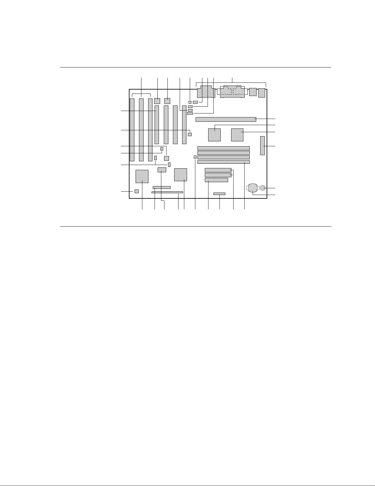
1.3 Motherboard Components
Motherboard Description
C
BA
G
H
F
IED
EE
J
K
DD
CC
L
M
BB
AA
Z
X S
Y
W
V
U
R
PQT
N
O
OM05640
Figure 1. Motherboard Components
A. ISA connectors L. Intel SB82441FX (PMC) V. Front panel header
B. Optional Yamaha OPL4-ML
component
C. Optional Yamaha OPL3-SA3
component
D. CD-ROM audio connector O. Battery Y. National PC87307VUL I/O
E. Telephony connector P. SIMM sockets Z. Fan 1 header
F. Wavetable header Q. IDE connectors AA. Optional Yamaha wavetable
G. Telephony connector R. GP I/O header BB. Chassis security header
H. Line In connector S. Floppy drive connector CC. Optional management
I. Back panel I/O connectors T. Hard disk LED (HDD LED)
J. Slot 1 processor connector U. Intel SB82371SB (PIIX3) EE. PCI connectors
K. Intel SB82442FX (DBX)
M. Power connector W. 2 Mbit TSOP flash device
N. Speaker X. Configuration jumper block
controller
module headers
extension hardware
DD. Fan 3 header
header
11
Page 12
PD440FX Technical Product Specification
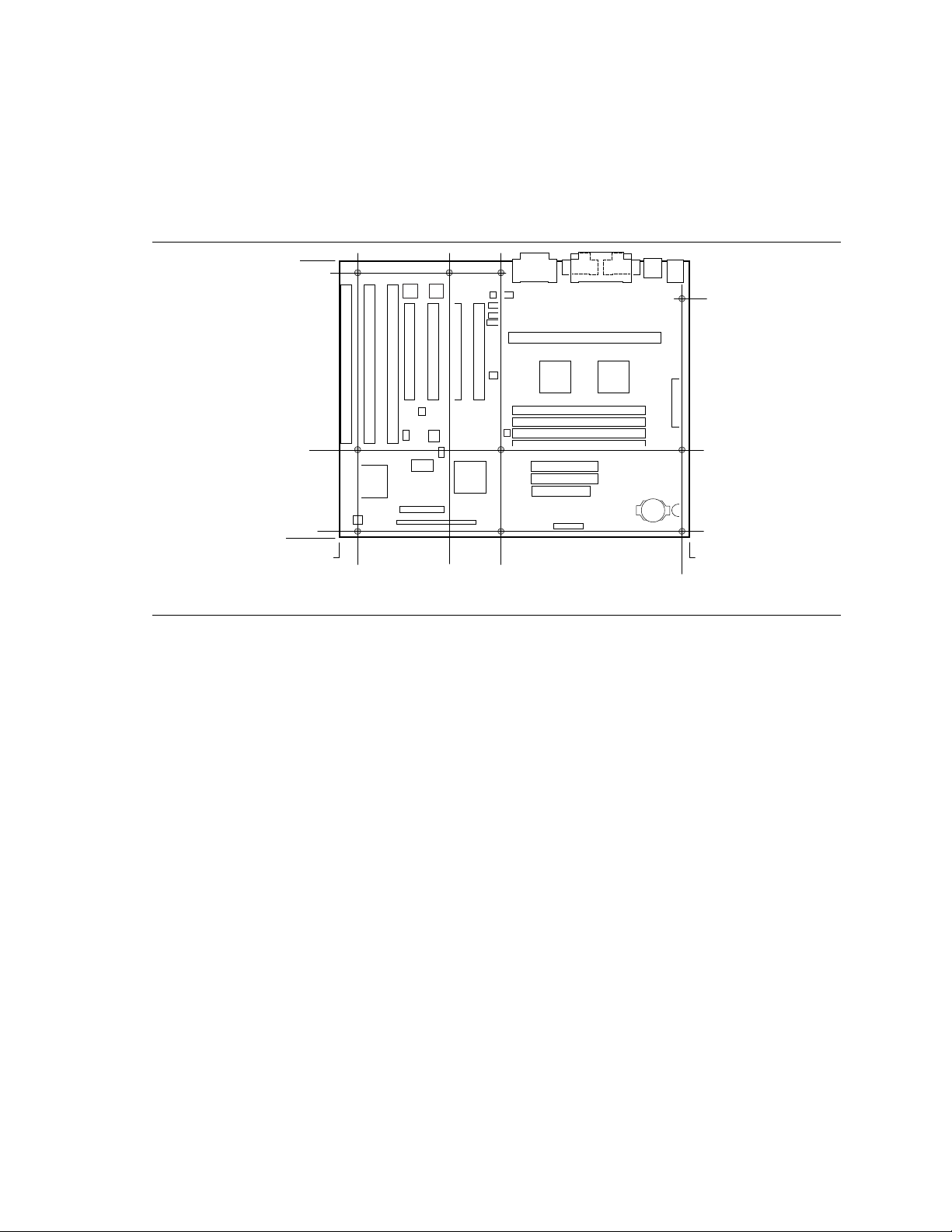
1.4 Form Factor
The motherboard is designed to fit into an ATX form factor chassis. Figure 2 illustrates the
mechanical form factor for the motherboard. Location of the I/O connectors and mounting holes
are in strict compliance with the ATX specification (see Section 6.2).
9.35
8.95
8.05
2.85
0.25
0.0
0.65
0.0
3.10 4.90
Figure 2. Motherboard Dimensions
11.35
11.10
OM05641
12
Page 13
Motherboard Description
1.5 I/O Shield
The back panel I/O shield for the PD440FX motherboard must meet specific dimensional and
material requirements. Systems based on this motherboard need the back panel I/O shield in order
to pass certification testing. Figure 3 shows the critical dimensions of the chassis-dependent I/O
shield. Figure 4 shows the critical dimensions of the chassis-independent I/O shield. Both figures
indicate the position of each cutout. Additional design considerations for I/O shields relative to
chassis requirements are described in the ATX specification. See Section 6.2 for information about
the ATX specification.
NOTE
✏
An I/O shield specifically designed for the Intel ATX chassis is available from Intel.
4.610
1.590
0.295
0.458
1.955
0.133
0.597
0.200
0.478
1.407
0.768
1.158
0.671
0.395
0.553
0.990
1.911
2.184
3.327
4.735
0.193
Note: Material = 0.010 ±.0.001 Thick Stainless Steel, Half Hard
4.899
5.391
5.883
6.533
0.652
2.055
0.050
2.326
2.023
0.120
Left-end View
0.306 Dia (3)
0.666
OM05669
Figure 3. Back Panel I/O Shield Dimensions (ATX Chassis-Dependent)
13
Page 14

PD440FX Technical Product Specification
NOTE
✏
A chassis-independent I/O shield designed to be compliant with the ATX chassis specification 2.01
is available from Intel.
0.039 Dia
0.945
0.279
0.00
0.472
0.464
0.685
0.945
0.00
0.134
0.442
0.911
Note: Material = 0.010 ±.0.001
Thick Stainless Steel, Half Hard
1.798
2.070
1.889
1.767
0.122
3.214
4.618
4.783
Right-end View
5.275
Figure 4. Back Panel I/O Shield Dimensions (ATX Chassis-Independent)
5.767
0.464
0.306 Dia (3)
6.255
OM05734
14
Page 15

Motherboard Description
1.6 Microprocessor
The motherboard supports a single Pentium II processor operating at 2.1 V to 3.5 V. The
motherboard’s voltage regulator is automatically programmed by the processor’s VID pins to
provide the required voltage. The motherboard operates with processors that run internally at
233 or 266 MHz and have either a 256 KB or 512 KB second-level cache.
The processor implements the MMX technology and maintains full backward compatibility with
the 8086, 80286, Intel386, Intel486, Pentium processor, and Pentium Pro processors. The
processor’s numeric coprocessor significantly increases the speed of floating-point operations and
complies with ANSI/IEEE standard 754-1985.
1.6.1 Microprocessor Packaging
The processor is packaged in an S.E.C. cartridge. The S.E.C. cartridge includes the processor core,
the second-level cache, a thermal plate, and a back cover.
The processor connects to the motherboard through the Slot 1 processor connector, a 242-pin edge
connector. When the processor is mounted in Slot 1, it is secured by a retention mechanism
attached to the motherboard. The processor’s heat sink is stabilized by a heat-sink support that is
attached to the motherboard.
1.6.2 Second Level Cache
The second-level cache is located on the substrate of the S.E.C. cartridge. The cache includes burst
pipelined synchronous static RAM (BSRAM) and tag RAM. There can be two or four BSRAM
components totaling 256 KB or 512 KB in size. All supported onboard memory can be cached.
15
Page 16

PD440FX Technical Product Specification
1.7 Main Memory
The motherboard has four SIMM sockets arranged in two banks: bank 0 and bank 1. Each bank
has two sockets and provides a 64/72-bit wide data path. SIMMs in the same bank must be the
same type (EDO, nonparity, parity, ECC), size, and speed; SIMMs in different banks may differ in
type, size, and speed. SIMMs must be installed in both sockets of a bank, and at least one bank
must be filled for the motherboard to work. The minimum memory size is 8 MB, and the
maximum size is 256 MB. The BIOS automatically detects memory type and size, so no jumper
settings are required.
The motherboard supports the following:
• 72-pin SIMM modules with tin-plated contacts only
• 50 ns or 60 ns DRAM speed only
• EDO SIMMs only
• Nonparity, parity, or ECC SIMMs
• 5 V-memory only
• Single- or double-sided SIMMs
The motherboard supports SIMMs in the following sizes:
Table 1. SIMM Sizes and Configurations
SIMM Size Nonparity Configuration Parity and ECC Configuration
4 MB 1 x 32 1 x 36
8 MB 2 x 32 2 x 36
16 MB 4 x 32 4 x 36
32 MB 8 x 32 8 x 36
64 MB 16 x 32 16 x 36
1.7.1 EDO DRAM
EDO DRAM improves memory-read performance by holding the memory data valid until the next
falling edge of the CAS# signal. With EDO DRAM, the CAS# precharge overlaps the data-valid
time, which allows the CAS# signal to negate earlier while still satisfying the memory data-valid
window.
16
Page 17

Motherboard Description
1.7.2 Parity/ECC DRAM
Memory error checking and correction supports the following operations:
• Parity memory operationdetects single-bit errors but does not correct the errors.
• Error checking and correcting (ECC) operationdetects single-bit and double-bit errors, and
corrects single-bit errors.
Use parity and ECC memory as follows:
• Parity and ECC SIMMs must not be mixed in the same bank.
• The 82441FX (PMC) memory controller automatically detects the presence of parity and ECC
SIMMs (36-bit modules) and treats them identically.
• Parity and ECC operations are supported with parity or ECC SIMMs.
• Use the Setup program to enable parity or ECC support. See Section 4.2.32 for information
about enabling parity or ECC support.
• If any nonparity SIMMs are installed, the memory operates in nonparity mode only. The Setup
options for selecting parity or ECC mode do not appear.
The following table describes the effect of using Setup to put each memory type in each supported
mode. Whenever ECC mode is selected in Setup, some loss in memory performance occurs.
Table 2. Memory Error-Detection Modes in the Setup Program
SIMM Type Disabled Parity ECC
Nonparity SIMMs No error detection N/A N/A
Parity SIMMs No error detection Single-bit error detection Single-bit error correction,
double-bit error detection
ECC SIMMs No error detection Single-bit error detection Single-bit error correction,
double-bit error detection
17
Page 18

PD440FX Technical Product Specification
1.8 Chipset
The Intel 82440FX PCIset consists of the 82441FX PCI bridge and memory controller (PMC) and
the 82442FX data bus accelerator (DBX). The Intel 82371SB PCI ISA/IDE Xccelerator (PIIX3)
bridge provides the connection between the ISA and PCI buses.
1.8.1 82441FX PCI Bridge and Memory Controller (PMC)
The PMC provides bus-control signals and address paths for transfers between the host bus, PCI
bus, and main memory. During host-to-PCI cycles, the PMC controls the PCI protocol. The PMC
also receives addresses from PCI bus initiators for PCI-to-DRAM transfers. The 82441FX comes
in a 208-pin PQFP package and provides the following features:
• Microprocessor interface control
Processor host bus speed up to 66 MHz
32-bit addressing
• Integrated DRAM controller
64/72-bit noninterleaved path to memory with ECC support
Support for EDO DRAM
8 MB to 256 MB main memory
• Fully-synchronous PCI bus interface
Compliant with the PCI specification revision 2.1 (see Section 6.2)
33 MHz PCI-bus speed
PCI-to-DRAM speed greater than 100 MB/sec
• Data Buffering
Host-to-DRAM and PCI-to-DRAM write-data buffering
Write-combining support for host-to-PCI burst writes
1.8.2 82442FX Data Bus Accelerator (DBX)
The DBX connects to the 64-bit processor data bus, the 64/72 bit memory-data bus, and the 16-bit
PMC private-data bus. The DBX works in parallel with the PMC to provide a high-performance
memory subsystem. The DBX comes in a 208-pin PQFP package.
1.8.3 82371SB PCI/ISA IDE Xccelerator (PIIX3)
The PIIX3 provides the interface between the PCI and ISA buses. The 82371SB integrates a busmaster, dual-channel fast-IDE interface capable of supporting up to four devices, a USB host/hub
controller, and many of the functions of ISA-based PC systems. The PIIX3 comes in a 208-pin
PQFP package and provides the following features:
• Interface between the PCI bus and ISA bus that is fully-compatible with ISA bus master and
slave interface
• Integrated fast IDE interface
Support for up to four devices with separate master/slave mode support
PIO Mode 4 transfers up to 16 MB/sec
Integrated 8 x 32-bit buffer for bus-master IDE PCI burst transfers
18
Page 19

• Universal serial bus (USB)
Host/hub controller
Support for two USB ports
• Enhanced DMA controller
Four 8-bit DMA channels
Three 16-bit DMA channels
Compatible and fast type-F DMA transfers
• Interval Timer
Three 8-bit timer/counters
• Interrupt Controller
Two eight-channel interrupt controllers
PCI-to-AT interrupt mapping circuitry
ISA refresh address generation
PCI/ISA bus arbitration circuitry
NMI logic
• Power Management
Programmable system management interrupt (SMI)
Motherboard Description
1.8.4 Universal Serial Bus (USB) Support
The motherboard features two USB ports that permit the direct connection of two USB peripherals,
one to each port. For more than two USB devices, an external hub can be connected to either of
the built-in ports. The motherboard fully supports the universal host controller interface (UHCI)
and uses software drivers that are UHCI-compatible. See Section 6.2 for information about the
USB specification. Features of USB include:
• Self-identifying peripherals that can be hot-plugged
• Automatic mapping of function to driver and configuration
• Support for isochronous and asynchronous transfer types over the same set of wires
• Support for up to 127 physical devices
• Guaranteed bandwidth and low latencies appropriate for telephony, audio, and other
applications
• Error-handling and fault-recovery mechanisms built into the protocol
NOTE
✏
Computer systems that have an unshielded cable attached to a USB port may not meet FCC Class
B requirements, even if no device or a low-speed (sub-channel) USB device is attached to the
cable. Use shielded cable that meets the requirements for high-speed (fully-rated) devices.
19
Page 20

PD440FX Technical Product Specification
1.8.5 IDE Support
The motherboard has two independent bus-mastering PCI IDE interfaces that support PIO Mode 3,
PIO Mode 4, and ATAPI devices (e.g., CD-ROM). The BIOS supports logical block addressing
(LBA) and extended cylinder head sector (ECHS) translation modes. IDE device transfer rate and
translation mode are automatically detected by the BIOS.
Usually programmed I/O operations require a substantial amount of processor bandwidth.
However, in multitasking operating systems, the bandwidth freed by bus mastering IDE can be
devoted to other tasks while disk transfers are occurring.
1.9 Super I/O Controller
The PC87307 Super I/O Controller from National Semiconductor is an ISA Plug and Play
compatible (see Section 6.2), multifunction I/O device that provides the following features:
• Serial ports:
Two 16450/16550A-software compatible UARTs
Internal send/receive 16-byte FIFO buffer
Four internal 8-bit DMA options for the UART with SIR support (USI)
• Multimode bidirectional parallel port
Standard mode, IBM and Centronics compatible
Enhanced parallel port (EPP) mode with BIOS and driver support
High-speed extended capabilities port (ECP) mode
• Floppy disk controller
DP8473 and N82077 compatible
16-byte FIFO
PS/2
High-performance digital data separator (DDS)
PC-AT
• Keyboard and mouse controller
Industry standard 8042A compatible
General-purpose microcontroller
8-bit internal data bus
• Real-time clock
DS1287 and MC146818 compatible
Accurate within ± 13 minutes/year at 25 ºC with 5 V applied
Includes advanced power control (APC)
• Support for an IrDA and Consumer IR-compliant infrared interface
†
diagnostic-register support
†
and PS/2 drive-mode support
By default, the I/O controller interfaces are automatically configured during boot up. The I/O
controller can also be manually configured in the Setup program.
20
Page 21

Motherboard Description
1.9.1 Serial Ports
The motherboard has two 9-pin D-Sub serial port connectors located on the back panel. The 16450
and 16550A compatible UARTs support data transfers at speeds up to 921.6 Kbaud, while the
extended UART mode supports data rates up to 1.5 Mbaud.
1.9.2 Parallel Port
The connector for the multimode bidirectional parallel port is a 25-pin D-Sub connector located on
the back panel of the motherboard. In the Setup program, the parallel port can be configured for
the following:
• Compatible (standard mode)
• Bidirectional (PS/2 compatible)
• Bidirectional EPP
• Bidirectional ECP
1.9.3 Floppy Controller
The I/O controller is software compatible with the DP8473 and N82077 floppy drive controllers
and supports both PC-AT and PS/2 modes. In the Setup program, the floppy interface can be
configured for the following floppy drive capacities and sizes:
• 360 KB, 5.25-inch
• 1.2 MB, 5.25-inch
• 720 KB, 3.5-inch
• 1.2 MB, 3.5-inch (driver required)
• 1.25/1.44 MB, 3.5-inch
• 2.88 MB, 3.5-inch
1.9.4 Keyboard and Mouse Interface
PS/2 keyboard and mouse connectors are located on the back panel of the motherboard. The 5 V
lines to these connectors are protected with a PolySwitch
reestablishes the connection after an over-current condition is removed. While this device
eliminates having to replace a fuse, power to the computer should be turned off before connecting
or disconnecting a keyboard or mouse.
NOTE
✏
You can plug the mouse and keyboard into either of the PS/2 connectors.
The keyboard controller contains the AMI Megakey keyboard and mouse controller code, provides
the keyboard and mouse control functions, and supports password protection for power on/reset. A
power on/reset password can be specified in the Setup program.
†
circuit that, like a self-healing fuse,
21
Page 22

PD440FX Technical Product Specification
The keyboard controller also supports the following hot-key sequences:
• <Ctrl><Alt><Del>: Software reset. This key sequence resets the computer’s software by
jumping to the beginning of the BIOS code and running the power-on self test (POST).
• <Ctrl><Alt><defined in Setup>: Power management. This key sequence invokes powermanaged mode, which reduces the computer’s power consumption while maintaining its ability
to service external interrupts.
• <Ctrl><Alt><defined in Setup>: Keyboard lock. This key sequence is a security feature that
locks the keyboard until the user password is entered. When keyboard lock is invoked, the
keyboard LEDs flash. To enable the keyboard-lock feature, a user password must be specified
in the Setup program.
1.9.5 Real-time Clock, CMOS RAM, and Battery
The real-time clock is compatible with DS1287 and MC146818 components. The clock provides a
time-of-day clock and a multicentury calendar with alarm features and century rollover. The realtime clock supports 242 bytes of battery-backed CMOS RAM in two banks that are reserved for
BIOS use.
The time, date, and CMOS values can be specified in the Setup program. The CMOS values can
be returned to their defaults by using the Setup program or by setting a configuration jumper on the
motherboard.
An external coin-cell battery powers the real-time clock and CMOS memory. When the computer
is not plugged into a wall socket, the battery has an estimated life of three years. When the
computer is plugged in, the 5 V standby current from the motherboard’s power supply extends the
life of the battery. The clock is accurate to ± 13 minutes/year at 25 ºC with 5 V applied.
1.9.6 Infrared Support
The motherboard has 6 pins located on the front panel I/O connector that support Hewlett Packard
HSDL-1000 compatible infrared (IR) transmitters and receivers. In the Setup program, Serial
Port 2 can be directed to a connected IR device. The connection can be used to transfer files to or
from portable devices like laptops, PDAs and printers. The Infrared Data Association (IrDA)
specification supports data transfers of 115 Kbaud at a distance of 1 meter. See Section 6.2 for
information about the IrDA specification.
1.9.6.1 Consumer Infrared Support
The motherboard has a dedicated signal pin located on the front panel I/O connector that supports
consumer infrared devices (remote controls). The signal pin supports receive only. Consumer
infrared devices can be used to control telephony functions and multimedia operations such as
volume and CD track changes. In this mode, data rates of up to 685.57 Kbaud are supported. A
software and hardware interface is needed to use this feature.
22
Page 23

Motherboard Description
1.10 Audio Subsystem
1.10.1 OPL3 Audio System
The onboard audio subsystem features the Yamaha OPL3-SA3 (YMF715) device. The features of
the device include the following:
• A 16-bit audio codec
• OPL3 FM synthesis
• An integrated 3-D enhanced stereo controller including all required analog components
• An interface for MPU-401 and a joystick
• Stereo analog-to-digital and digital-to-analog converters
• Analog mixing, anti-aliasing, and reconstruction filters
• Support for 16-bit address decoding
• Line, microphone, and monaural inputs
• ADPCM, A-law, or µlaw digital audio compression and decompression
• Full digital control of all mixer and volume control functions
• Software switching between rear panel Mic In and Line In connectors
• Plug and Play compatibility
• Sound Blaster
†
Pro and Windows Sound System compatibility
1.10.2 OPL4-ML Wavetable Synthesizer
The optional onboard Wavetable synthesizer features the single-chip OPL4-ML (YMF704). The
OPL4-ML integrates the OPL3 audio system, general MIDI processor, and Wavetable ROM into a
single component. The features of the device include the following:
• Complies with general MIDI system 1
• Interface compatible with MPU-401 UART mode
• FM synthesis compatible with the OPL3 audio system
• Wavetable synthesis generates up to 24 voices simultaneously
• 100-pin SQFP package (YMF704-S)
NOTE
✏
An optional OPL4-ML reference design module that can be plugged into the board may be
licensed from Yamaha Corporation.
1.10.3 Audio Subsystem Resources
The following table shows the IRQ, DMA channel, and base I/O address options for the audio
subsystem. Options are listed in order of preference specified by Yamaha. These options are
automatically chosen by the Plug and Play interface, so there are no default settings. Onboard
audio can be enabled or disabled in the Setup program.
23
Page 24

PD440FX Technical Product Specification
Table 3. Audio Subsystem Resources
IRQ
Resource
Sound Blaster
(DMA playback, DMA shared with Windows
Sound System capture)
Windows Sound System
(DMA playback)
MPU-401
(IRQ shared with Sound Blaster)
MIDI / Game Port 201h
†
AdLib
(Options)
10
7
5,7,9,10,11
5
11
5,7,9,10,11
DMA Channel
(Options)
1
0,1,3
0
0,1,3
1.10.4 Audio Drivers and Utilities
Audio software and utilities are available from Intel’s World Wide Web site (see Section 6.1).
Audio driver support is provided for Microsoft Windows
†
Windows NT
(versions 3.51 and 4.0), and IBM OS/2† Warp (versions 3.0 and 4.0) operating
systems.
†
3.1, Microsoft Windows 95, Microsoft
I/O Address
(Options)
220h
240h
220-280h
530h
E80h
530-F48h
330h
300h
300-334h
201-20Fh
388h
388-3F8h
1.10.5 Audio Connectors
Audio connectors include the following:
• Back panel audio jacks (Line In, Line Out, Mic In)
• CD-ROM audio connector
• Telephony connectors (a 1 x 4 pin and a 2 x 2 pin)
• Line In connector
• Wavetable connector
1.10.5.1 CD-ROM Audio Connector
A 1 x 4-pin connector is available for connecting an internal CD-ROM drive to the audio
subsystem’s mixer. The connector is compatible with most cables supplied with ATAPI CD-ROM
drives designed to connect to audio add-in cards.
1.10.5.2 Telephony Connectors
Telephony support is available for connecting the monaural audio signals of an internal telephony
device to the motherboard’s audio subsystem. A monaural audio-in and audio-out signal interface
is necessary for telephony applications such as speakerphones, fax/modem, and answering
machines. Two different interface headers are available for this application: a general telephony
interface with a 1 x 4-pin ATAPI type connector and a telephony interface with a 2 x 2-pin header.
See Section 1.12 for connector reference numbers and pinouts.
24
Page 25

Motherboard Description
1.10.5.3 Line In Connector
The Line In connector is available for connecting left and right channel signals of an internal audio
device to the motherboard’s audio subsystem. An audio-in signal interface of this type is necessary
for applications such as TV tuners. A general audio interface is provided with a 1 x 4-pin ATAPI
type connector. See Section 1.12 for connector reference numbers and pinouts.
1.10.5.4 Hardware Wavetable Connector
A 2 x 4-pin header supports wavetable add-in cards. Most wavetable add-in cards are installed in a
standard ISA slot, and a cable is then routed from the card to this header.
Compatible wavetable cards are available from several vendors. The ICS WaveFront and the
CrystaLake Series 2000 wavetable product families offer general MIDI-compatible audio
operation.
1.11 Management Extension Hardware
The optional management extension hardware provides low-cost instrumentation capabilities
designed to reduce the total cost of owning a PC. The hardware implementation is a single-chip
ASIC. Features include:
• An integrated temperature sensor
• Fan speed sensors for up to three fans
• Power supply voltage monitoring to detect levels above or below acceptable values
• Header for an external chassis-security feature
See Section 6.2 for information about where to get the specification for the management extension
hardware.
NOTE
✏
When suggested ratings for temperature, fan speed, or voltage are exceeded, an interrupt is
activated.
1.11.1 Chassis Security Header (J6C1)
The PD440FX motherboard supports the chassis-security feature of the management extension
hardware by means of a mechanical switch attached to the motherboard through a 1 x 2-pin chassis
security header (J6C1). The mechanical switch is open for normal computer operation. See
Section 1.12 for chassis security header pinouts.
1.11.2 GP I/O Header
This header is not supported by the standard PD440FX BIOS. See the pinouts for this header on
page 28.
25
Page 26
PD440FX Technical Product Specification
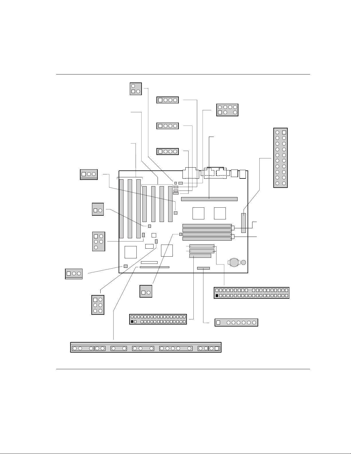
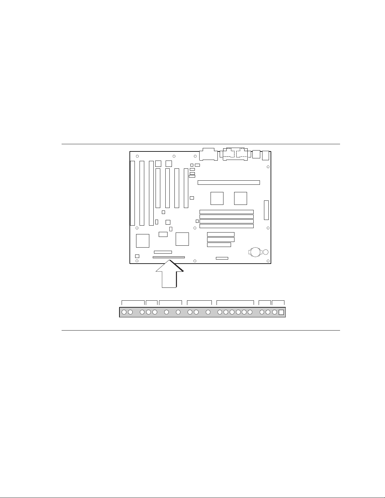
1.12 Motherboard Connectors
The following figure shows the connectors on the motherboard.
2
Telephony
J4F1
1
Fan 3
Chassis
Security
Yamaha
Wavetable
Module
J2F1
13
PCI
Connectors(4)
J4C1, J4D1
J4E1, J4E2
ISA
Connectors(3)
J4A1, J4B1
J4B2
3
J6C1
12
1
J7C1
J2F3
1
4
Telephony
J2F6
14
CD-ROM Audio
J3F1
14
Line In
Sec
Pri
Wavetable
2
1
8
7
J2F2
Slot 1
Processor
Card Connector
J4A1
J6M1
11
20
Power
Bank 0 DRAM
(J6J1, J6J2)
Bank 1 DRAM
(J7J1, J7J2)
1
10
J9A1
1
Fan 1
Yamaha
Wavetable
Module
J9D1
27
3
1
J7D1
J6F1
Hard Disk LED
(HDD LED)
12
J8H3
234
1335
Floppy
2
139
J10H1
18
GP I/O
1
PCI IDE(2)
4020
J8H1
J8H2
Front Panel I/O Connectors
OM05645
Figure 5. Motherboard Connectors
26
Page 27

Table 4. Telephony Connector (J2F1)
Pin Signal Name
1 Ground
2 MONO_IN (from external device)
3 MONO_OUT (to external device)
4 Key
Table 5. Telephony Connector (J2F3)
Pin Signal Name
1 MONO_IN (from external device)
2 Ground
3 Ground
4 MONO_OUT (to external device)
Table 6. CD-ROM Audio Connector (J2F6)
Motherboard Description
Pin Signal Name
1 Ground
2 CD_IN-Left
3 Ground
4 CD_IN-Right
Table 7. Line In Connector (J3F1)
Pin Signal Name
1 Left Line In
2 Ground
3 Ground
4 Right Line In (monaural)
Table 8. Wavetable Connector (J2F2)
Pin Signal Name Pin Signal Name
1 Wave In Right 2 Ground
3 Wave In Left 4 Ground
5 Key 6 Ground
7 Not connected 8 MIDI Out (from Host)
Note: This connector is a 2 x 4 male, 0.100” centerline stake header with 0.025” square pins. The mating connector is a
Berg 71600-308 or equivalent.
27
Page 28

PD440FX Technical Product Specification
Table 9. Hard Disk LED (HDD LED) Header
(J6F1)
Pin Signal Name
1 DRV_ACT#
2 No connect
Table 10. Fan 1 Header (J9A1)
Pin Signal Name
1 Ground
2 +12 V
3 FAN_SEN
Table 11. Fan 3 Header (J4F1)
Pin Signal Name
1 Ground
2 +12 V
3 FAN_SEN
Table 12. Chassis Security Header (J6C1)
Pin Signal Name
1 Ground
2 CHS_SEC
Table 13. GP I/O Header (J10H1)
Pin Signal Name
1 Vcc
2 Key
3 GP1_7
4 Ground
5 GP1_2
6 Ground
7 GP1_1
8 Ground
28
Page 29

Motherboard Description
Table 14. Yamaha Wavetable Module Connectors (J7C1 and J7D1)
Connector (J7D1) Connector (J7C1)
Pin Signal Name Pin Signal Name
1 EXTEN# 1 RSTDRV
2 SIN 2 Vcc
3 Vcc 3 AUD33MHZ
4 Ground 4 MIDI Out
5 BCK 5 Ground
6 LACK 6 Key
Note: There are two 2 x 3 headers in a standard position to connect to the Yamaha wavetable module.
Table 15. Floppy Drive Connector (J8H3)
Pin Signal Name Pin Signal Name
1 Ground 2 DENSEL
3 Ground 4 Reserved
5 Key 6 FDEDIN
7 Ground 8 FDINDX# (Index)
9 Ground 10 FDM00# (Motor Enable A)
11 Ground 12 FDDS1# (Drive Select B)
13 Ground 14 FDDS0# (Drive Select A)
15 Ground 16 FDM01# (Motor Enable B)
17 MSEN1 18 FDDIR# (Stepper Motor Direction)
19 Ground 20 FDSTEP# (Step Pulse)
21 Ground 22 FDWD# (Write Data)
23 Ground 24 FDWE# (Write Enable)
25 Ground 26 FDTRK0# (Track 0)
27 MSEN0 28 FDWPD# (Write Protect)
29 Ground 30 FDRDATA# (Read Data)
31 Ground 32 FDHEAD# (Side 1 Select)
33 Ground 34 DSKCHG# (Diskette Change)
29
Page 30

PD440FX Technical Product Specification
Table 16. PCI IDE Connectors (J8H1, J8H2)
Pin Signal Name Pin Signal Name
1 Reset IDE 2 Ground
3 Data 7 4 Data 8
5 Data 6 6 Data 9
7 Data 5 8 Data 10
9 Data 4 10 Data 11
11 Data 3 12 Data 12
13 Data 2 14 Data 13
15 Data 1 16 Data 14
17 Data 0 18 Data 15
19 Ground 20 Key
21 DDRQ0 [DDRQ1] 22 Ground
23 I/O Write# 24 Ground
25 I/O Read# 26 Ground
27 IORDY 28 P_ALE [S_ALE](Cable Select pullup)
29 DDACK0# [DDACK1#] 30 Ground
31 IRQ 14 [IRQ 15] 32 Reserved
33 Address 1 34 Reserved
35 Address 0 36 Address 2
37 Chip Select 1P# [Chip Select 1S#] 38 Chip Select 3P# [Chip Select 3S#]
39 Activity# 40 Ground
Note: Signal names in brackets ([ ]) are for the secondary IDE connector.
30
Page 31

Motherboard Description
1.12.1 Power Supply Connector
When used with a power supply that supports remote power on/off, the motherboard can turn off
the system power through software control.
To enable soft-off control in software, advanced power management must be enabled in the Setup
program and in the operating system. When the system BIOS receives the correct APM command
from the operating system, the BIOS turns off power to the computer. For example, in the
Windows 95 Start menu, select Shutdown to turn off the power.
With Auto Start On AC loss enabled in the Setup program and soft-off enabled, if power to the
computer is interrupted by a power outage or a disconnected power cord, when power resumes, the
computer returns to the on or off state it was in before power was interrupted.
Table 17. Power Supply Connector (J6M1)
Motherboard
Pin
1 1 +3.3 V 14 11 +3.3 V
2 2 +3.3 V 15 12 -12 V
3 3 Ground 16 13 Ground
4 4 +5 V 17 14 PW_ON#
5 5 Ground 18 15 Ground
6 6 +5 V 19 16 Ground
7 7 Ground 20 17 Ground
8 8 PWRGD (Power
9 9 +5 VSB (Standby for
10 10 +12 V 23 20 +5 V
11 -12 V 24 +5 V
12 Ground 25 Key
13 Ground 26 +5 V
Note: Pins and signals in gray are for optional connector placement.
Connector
Pin Signal Name
Good)
real-time clock)
Motherboard
Pin
21 18 -5 V
22 19 +5 V
Connector
Pin Signal Name
31
Page 32
PD440FX Technical Product Specification
1.12.2 Front Panel Connectors
The front panel connector includes headers for these I/O connections:
• Speaker
• Reset switch
• Power LED
• Hard drive activity LED (HD LED)
• Infrared (IrDA) port
• Sleep switch
• Power switch
Speaker Reset Pwr LED HD LED Infrared Sleep Pwr On
27 1
OM05644
Figure 6. Front Panel I/O Connectors
32
Page 33

Table 18. Front Panel I/O Connectors (J9D1)
Pin Signal Name Connector
1 SW_ON# power on
2 Ground
3 SLEEP sleep/resume
4 SLEEP_PU (pullup)
5 No connect none
6 +5 V IrDA
7 Key
8 IrRX
9 Ground
10 IrTX
11 CONIR (Consumer IR)
12 No connect none
13 HD_PWR +5 V HD LED
14 Key
15 HD Active#
16 HD_PWR
17 No connect/Key none
18 Ground sleep/power
LED
19 Key
20 PWR_LED
21 No connect/Key none
22 Ground reset
23 SW_RST
24 Ground speaker
25 Key
26 PIEZO_IN
27 SPKR_HDR
Motherboard Description
33
Page 34

PD440FX Technical Product Specification
1.12.2.1 Power On Connector
This header must be connected to a front panel power switch. The switch must pull the SW_ON#
pin to ground for at least 50 ms to signal the power supply to switch on or off. (The time
requirement is due to the motherboard’s internal debounce circuitry.) At least two seconds must
pass before the motherboard will recognize another on/off signal.
1.12.2.2 Sleep/Resume Header
When APM is enabled in the system BIOS and the operating system’s APM driver is loaded, the
system can enter sleep (standby) mode in one of three ways:
• Optional front panel sleep/resume button
• Hot-key defined in the Setup program
• System inactivity timeout
Default timeout is 10 minutes
Can be changed in the Setup program
A sleep/resume switch is supported by the 2-pin header located on the front panel I/O connector.
The front panel sleep/resume switch must be a momentary SPST type that is normally open.
Closing the sleep/resume switch generates a system management interrupt (SMI) to the processor;
the processor immediately goes into system management mode (SMM). While in sleep mode, the
system is fully capable of responding to and servicing external interrupts (such as an incoming fax)
even though the monitor turns on only if a keyboard or mouse interrupt occurs. To resume system
activity, press the sleep/resume button again, use the keyboard, or use the mouse.
1.12.2.3 Infrared Connector
The Serial Port 2 can be configured to support an IrDA module connected to this 6-pin header.
After configuring the IrDA interface, files can be transferred to or from portable devices such as
laptops, PDAs, and printers using application software.
1.12.2.4 Onboard IDE Hard Disk LED (HD LED) Header
This header can be connected to an LED to provide a visual indicator that data is being read from
or written to an IDE hard drive. For the LED to function properly, the IDE drive must be
connected to the onboard IDE controller on the motherboard. See Section 1.12.3 for information
about the header for an add-in hard-drive controller card.
1.12.2.5 Sleep/Power LED Header
You can connect this header to an LED that will light when the computer is powered on. This
LED will also blink when the computer is in a power-managed state.
1.12.2.6 Reset Header
You can connect this header to a momentary SPST type switch that is normally open. When the
switch is closed, the board resets and runs the POST.
34
Page 35

Motherboard Description
1.12.2.7 Speaker Header
A speaker may be installed on the motherboard as a manufacturing option. The speaker option
includes a jumper on pins 26-27 of the front panel connector. You can disable the onboard speaker
by removing the jumper, and you can connect an offboard speaker in its place. The speaker
(onboard or offboard) provides error beep code information during the POST in the event that the
computer cannot use the video interface. The speaker is not connected to the audio subsystem and
does not receive output from the audio subsystem.
1.12.3 Hard Drive LED (HDD LED) Header
The hard drive LED header is a 1 x 2-pin header (J6F1) that allows add-in controller applications
(i.e., a SCSI controller for additional drive capacity) to use the same LED as the onboard frontpanel LED. This header can be connected to the LED output of the add-in controller card. The
LED will indicate when data is being read or written using the add-in controller. See
Section 1.12.2.4 for information about the onboard IDE hard disk LED header.
35
Page 36
PD440FX Technical Product Specification
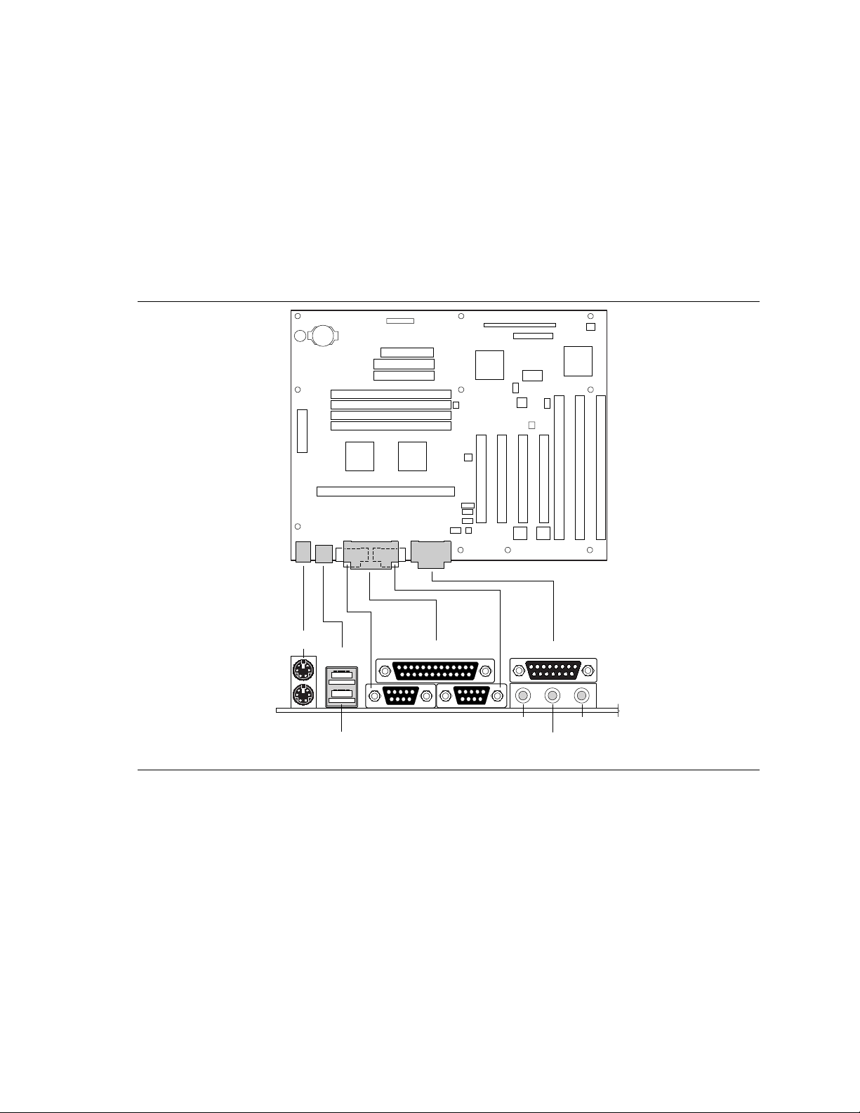
1.12.4 Back Panel Connectors
Figure 7 shows the location of the back panel I/O connectors, which include:
• PS/2-style keyboard and mouse connectors
• Two USB connectors
• One parallel port
• Two serial ports
• MIDI/game port
• External audio jacks: Line Out, Line In, and Mic In
Keyboard
USB 1
Mouse Serial
USB 0
Port 1
Figure 7. Back Panel I/O Connectors
Parallel Port
Serial
Port 2
MIDI/Game Port
Line Out Mic In
Line In
OM05642
36
Page 37

Table 19. PS/2 Keyboard or Mouse Connectors (J1M1)
Pin Signal Name
1 Data
2 No connect
3 Ground
4 +5 V (fused)
5 Clock
6 No connect
Table 20. USB Connectors (J1L1)
Pin Signal Name
1 Power (fused)
2 USBP0# [USBP1#]
3 USBP0 [USBP1]
4 Ground
Motherboard Description
Table 21. Serial Port Connectors (J1J1, J1K1)
Pin Signal Name
1 DCD
2 Serial In#
3 Serial Out#
4 DTR#
5 Ground
6 DSR#
7 RTS#
8 CTS#
9 RI# (ring-in)
37
Page 38

PD440FX Technical Product Specification
Table 22. Parallel Port Connector (J1J2)
Pin Signal Name Pin Signal Name
1 Strobe# 14 Auto Feed#
2 Data bit 0 15 Fault#
3 Data bit 1 16 INIT#
4 Data bit 2 17 SLCT IN#
5 Data bit 3 18 Ground
6 Data bit 4 19 Ground
7 Data bit 5 20 Ground
8 Data bit 6 21 Ground
9 Data bit 7 22 Ground
10 ACK# 23 Ground
11 Busy 24 Ground
12 Error 25 Ground
13 Select
Table 23. Audio Line Out Connector (J1G1)
Pin Signal Name
Sleeve Ground
Tip Audio Left Out
Ring Audio Right Out
Table 24. Audio Line In Connector (J1G1)
Pin Signal Name
Sleeve Ground
Tip Audio Left In
Ring Audio Right In
Table 25. Audio Mic In Connector (J1G1)
Pin Signal Name
Sleeve Ground
Tip Mono In
38
Page 39

Motherboard Description
Table 26. MIDI / Game Port Connector(J1G1)
Pin Signal Name Pin Signal Name
1 +5 V (fused) 9 +5 V (fused)
2 GP4 (JSBUTO) 10 GP6 (JSBUT2)
3 GP0 (JSX1R) 11 GP2 (JSX2R)
4 Ground 12 MIDI-OUTR
5 Ground 13 GP3 (JSY2R)
6 GP1 (JSY1R) 14 GP7 (JSBUT3)
7 GP5 (JSBUT1) 15 MIDI-INR
8 +5 V (fused)
Note: Items in parentheses are alternate versions of signal names.
1.12.5 Add-in Board Expansion Connectors
The motherboard contains three PCI slots, two ISA slots, and one shared slot (for a PCI or ISA
card). The PCI bus supports up to four bus masters through the four PCI connectors (see
Section 6.2 for information about the PCI specification).
39
Page 40

PD440FX Technical Product Specification
Table 27. PCI Bus Connectors
Pin Signal Name Pin Signal Name Pin Signal Name Pin Signal Name
A1 Ground (TRST#)* B1 -12 V A32 AD16 B32 AD17
A2 +12 V B2 Ground (TCK)* A33 +3.3 V B33 C/BE2#
A3 +5 V (TMS)* B3 Ground A34 FRAME# B34 Ground
A4 +5 V (TDI)* B4 no connect
(TDO)*
A5 +5 V B5 +5 V A36 TRDY# B36 +3.3 V
A6 INTA# B6 +5 V A37 Ground B37 DEVSEL#
A7 INTC# B7 INTB# A38 STOP# B38 Ground
A8 +5 V B8 INTD# A39 +3.3 V B39 LOCK#
A9 Reserved B9 PRSNT1# A40 SDONE B40 PERR#
A10 +5 V (I/O) B10 Reserved A41 SBO# B41 +3.3 V
A11 Reserved B11 PRSNT2# A42 Ground B42 SERR#
A12 Ground B12 Ground A43 PAR B43 +3.3 V
A13 Ground B13 Ground A44 AD15 B44 C/BE1#
A14 Reserved B14 Reserved A45 +3.3 V B45 AD14
A15 RST# B15 Ground A46 AD13 B46 Ground
A16 +5 V (I/O) B16 CLK A47 AD11 B47 AD12
A17 GNT# B17 Ground A48 Ground B48 AD10
A18 Ground B18 REQ# A49 AD09 B49 Ground
A19 Reserved B19 +5 V (I/O) A50 Key B50 Key
A20 AD30 B20 AD31 A51 Key B51 Key
A21 +3.3 V B21 AD29 A52 C/BE0# B52 AD08
A22 AD28 B22 Ground A53 +3.3 V B53 AD07
A23 AD26 B23 AD27 A54 AD06 B54 +3.3 V
A24 Ground B24 AD25 A55 AD04 B55 AD05
A25 AD24 B25 +3.3 V A56 Ground B56 AD03
A26 IDSEL B26 C/BE3# A57 AD02 B57 Ground
A27 +3.3 V B27 AD23 A58 AD00 B58 AD01
A28 AD22 B28 Ground A59 +5 V (I/O) B59 +5 V (I/O)
A29 AD20 B29 AD21 A60 REQ64C# B60 ACK64C#
A30 Ground B30 AD19 A61 +5 V B61 +5 V
A31 AD18 B31 +3.3 V A62 +5 V B62 +5 V
A35 Ground B35 IRDY#
* These signals (in parentheses) are optional in the PCI specification and are not implemented on this motherboard.
40
Page 41

Motherboard Description
Table 28. ISA Bus Connectors
Pin Signal Name Pin Signal Name
B1 Ground A1 IOCHK# (IOCHCK#)
B2 RESET (RESDRV) A2 SD7
B3 +5 V A3 SD6
B4 IRQ9 A4 SD5
B5 -5 V A5 SD4
B6 DRQ2 A6 SD3
B7 -12 V A7 SD2
B8 SRDY# (NOWS#) A8 SD1
B9 +12 V A9 SD0
B10 Ground A10 IOCHRDY (CHRDY)
B11 SMEMW# (SMWTC#) A11 AEN
B12 SMEMR# (SMRDC#) A12 SA19
B13 IOW# (IOWC#) A13 SA18
B14 IOR# (IORC#) A14 SA17
B15 DACK3# A15 SA16
B16 DRQ3 A16 SA15
B17 DACK1# A17 SA14
B18 DRQ1 A18 SA13
B19 REFRESH# A19 SA12
B20 BCLK A20 SA11
B21 IRQ7 A21 SA10
B22 IRQ6 A22 SA9
B23 IRQ5 A23 SA8
B24 IRQ4 A24 SA7
B25 IRQ3 A25 SA6
B26 DACK2# A26 SA5
B27 TC A27 SA4
B28 BALE A28 SA3
B29 +5 V A29 SA2
B30 OSC A30 SA1
B31 Ground A31 SA0
Key Key
D1 MEMCS16# (M16#) C1 SBHE#
D2 IOCS16# (IO16#) C2 LA23
D3 IRQ10 C3 LA22
Note: Items in parentheses are alternate versions of signal names.
continued ☛
41
Page 42

PD440FX Technical Product Specification
Table 28. ISA Bus Connectors (continued)
Pin Signal Name Pin Signal Name
D4 IRQ11 C4 LA21
D5 IRQ12 C5 LA20
D6 IRQ15 C6 LA19
D7 IRQ14 C7 LA18
D8 DACK0# C8 LA17
D9 DRQ0 C9 MEMR# (MRDC#)
D10 DACK5# C10 MEMW# (MWTC#)
D11 DRQ5 C11 SD8
D12 DACK6# C12 SD9
D13 DRQ6 C13 SD10
D14 DACK7# C14 SD11
D15 DRQ7 C15 SD12
D16 +5 V C16 SD13
D17 Master16# (MASTER#) C17 SD14
D18 Ground C18 SD15
Note: Items in parentheses are alternate versions of signal names.
42
Page 43

1.13 Jumper Settings
Figure 8 shows the location of jumper blocks on the motherboard.
Motherboard Description
A B C D
465
465
465
465
J9C1
1
32
321
321
321
OM05643
Figure 8. Jumper Locations
Table 29. Jumper Settings
Function Jumper J9C1 Configuration
Processor configuration A, B, C See Table 30
BIOS recovery A 5-6 Normal operation (default)
4-5 Recover BIOS
CMOS (NVRAM and ESCD) clear C 5-6 Keep (default)
4-5 Clear
Password clear D 1-2 Password clear/disabled
2-3 Password enabled (default)
BIOS Setup access D 5-6 Access enabled (default)
4-5 Access denied
* These jumpers also set the PCI and ISA bus frequencies.
43
Page 44

PD440FX Technical Product Specification
CAUTION
Do not move any of the jumpers with the power on. Always turn off the power and unplug the
power cord from the computer before changing jumpers.
1.13.1 Processor Configuration (J9C1-A, B, C)
These jumpers are for configuring the motherboard for the frequency of the installed processor.
Table 30 shows the jumper settings for each frequency and the corresponding host bus, PCI bus,
and ISA bus frequencies.
Table 30. Jumper Settings for Processor and Host Bus Frequencies
Host Bus
Processor
Freq. (MHz)
233 2-3 2-3 and 5-6 2-3 66 33 8.33 3.5
266 1-2 1-2 and 4-5 2-3 66 33 8.33 4
Note: All other jumper settings for internal processor frequencies on this motherboard are reserved.
Jumpers
J9C1-A
Jumpers
J9C1-B
Jumpers
J9C1-C
Freq.
(MHz)
PCI Bus
Freq.
(MHz)
ISA Bus
Freq.
(MHz)
Bus/Processor
Freq. Ratio
1.13.2 BIOS Recovery (J9C1-A)
This jumper is for recovering BIOS data from a diskette in the event of a catastrophic failure. The
default setting is pins 5-6 (normal operation). To recover the BIOS, turn off the computer, move
the jumper to pins 4-5, then turn on the computer to perform BIOS recovery. After recovery, turn
off the computer and return the jumper to pins 5-6 to restore normal operation. See Section 3.1.14
for more details.
1.13.3 CMOS Clear (J9C1-C)
This jumper is for resetting the CMOS settings to the default values. This procedure must be done
each time the system BIOS is updated. The default setting for this jumper is pins 5-6 (keep CMOS
settings). To reset the CMOS settings to the default values, turn off the computer, move the
jumper to pins 4-5, then turn on the computer. When the computer displays the message
“NVRAM cleared by jumper,” turn off the computer and return the jumper to pins 5-6 to restore
normal operation.
1.13.4 Password Clear (J9C1-D)
This jumper is for clearing the password if the password is forgotten. The default setting is
pins 2-3, (password enabled). To clear the password, turn off the computer, move the jumper to
pins 1-2, and turn on the computer. Then turn off the computer, and return the jumper to pins 2-3
to restore normal operation. If the jumper is in the 1-2 position (password disabled), you cannot
set a password.
1.13.5 BIOS Setup Access (J9C1-D)
This jumper is for enabling or disabling access to the Setup program. The default setting is
pins 5-6 (access enabled). To disable access to the Setup program, move the jumper to pins 4-5.
44
Page 45

Motherboard Description
1.14 Reliability
The Mean-Time-Between-Failures (MTBF) prediction is calculated using component and
subassembly random failure rates. The calculation is based on the Bellcore Reliability Prediction
Procedure, TR-NWT-000332, Issue 4, September 1991.
The MTBF prediction is for:
• Early identification of redesign or alternate component selection if cumulative failure rates
exceed reliability expectations.
• Reliability information for field service personnel to estimate repair rates and spares
requirements.
MTBF data is calculated from predicted data @ 55 °C.
The MTBF prediction for the PD440FX motherboard is 55,763 hours.
1.15 Environmental Specifications
Table 31 lists the environmental specifications for the motherboard.
Table 31. Motherboard Environmental Specifications
Parameter Specification
Temperature
Nonoperating -40 oC to +70 oC
Operating +0 oC to +55 oC
Vibration
Unpackaged 5 Hz to 20 Hz : 0.01g² Hz sloping up to 0.02 g² Hz
20 Hz to 500 Hz : 0.02g² Hz (flat)
Packaged 10 Hz to 40 Hz : 0.015g² Hz (flat)
40 Hz to 500 Hz : 0.015g² Hz sloping down to 0.00015 g² Hz
45
Page 46

PD440FX Technical Product Specification
1.16 Power Consumption
Table 32 lists the power specifications for a computer that contains the motherboard, a 266 MHz
Pentium II processor with 512 KB cache, 64 MB RAM, a 3.5-inch floppy drive, a 2.5 GB IDE
hard drive, and a PCI graphics card. This information is provided only as a guide for calculating
approximate power usage with additional resources added.
Values for the Windows 95 desktop mode are measured at 60 Hz refresh rate with 1 MB of
VRAM. AC watts are measured with a typical 200 W power supply, nominal input voltage and
frequency, and a true RMS wattmeter at the line input.
Table 32. Power Usage
Mode AC (watts) Out of 110 VAC Wall Outlet
DOS prompt, APM disabled 58.7 W
Windows 95 desktop, APM disabled 60.0 W
Windows 95 desktop, APM enabled, in SMM 28.0 W
1.16.1 Power Supply Considerations
For typical configurations, the motherboard is designed to operate with at least a 200 W power
supply (see Section 6.2 for the specification). A higher-wattage power supply should be used for
heavily-loaded configurations. The power supply must meet the following requirements:
• Rise time for power supply: 2 ms to 20 ms
• Minimum delay for reset to Power Good: 100 ms
• Minimum Powerdown warning: 1 ms
• 3.3 V output must reach its minimum regulation level within ± 20 ms of the +5 V output
reaching its minimum regulation level
Table 33. DC Voltage
DC Voltage Acceptable Tolerance
+3.3 V ± 5%
+5 V ± 5%
+5 V SB (standby) ± 5%
-5 V ± 5%
+12 V ± 5%
-12 V ± 5%
46
Page 47

Motherboard Description
1.17 Thermal Considerations
The following table provides maximum component case temperatures for motherboard components
that may be sensitive to thermal changes. Case temperatures may be affected by the motherboard’s
operating temperature, current load, or operating frequency. Maximum case temperatures are
important when considering proper airflow to cool the motherboard.
CAUTION
An ambient temperature that exceeds the motherboard’s maximum operating temperature by 5 oC
o
C may cause components to exceed their maximum case temperature. For information about
to 10
the motherboard’s maximum operating temperature, see the environmental specifications in
Section 1.15.
Table 34. Thermal Considerations for Motherboard Components
Component Maximum Case Temperature Motherboard Location
Pentium II processor 75 oC (thermal plate)
Intel SB82442FX (DBX) 85 oC (case) U5H1
Intel SB82441FX (PMC) 85 oC (case) U5K1
Intel SB82371SB (PIIX3) 85 oC (case) U8E1
NPN FET (4410) 105 oC (case) Q2K1, Q2K2, Q2K3, Q2K4
FET driver (MIC4427) 105 oC (case) U2H2, U3K2
The following figure shows motherboard components that may be sensitive to thermal changes.
FET Driver
(U2H2)
Intel SB82371SB (U8E1)
Figure 9. Thermally-sensitive Motherboard Components
NPN FET
(Q2K1, Q2K2,
Q2K3, Q2K4)
FET Driver
(U3K2)
Intel SB82442FX
(U5H1)
Intel SB822441FX
(U5K1)
OM06051
47
Page 48

PD440FX Technical Product Specification
1.18 Regulatory Compliance
Certification of the printed circuit assembly is provided as a convenience to OEM manufacturers.
Printed circuit assembly certification allows OEM manufacturers to treat the motherboard as a
single sub-assembly within the complete and final system level product being manufactured by the
OEM. With printed circuit assembly certification, improvements and changes made to the printed
circuit assembly over the life of the motherboard product are maintained by Intel. This simplifies
the system certification efforts by the OEM manufacturer.
1.18.1 Product Certification Markings
This printed circuit assembly complies with the following safety and EMI regulations when
correctly installed in a compatible host system. This printed circuit assembly has the following
product certification markings:
• UL Recognition Mark: UL Safety certification is identified with the UL File No. E139761 on
the component side of the board and the PB number on the solder side of the board. Board
material flammability is compliant with the 94V-1 or 94V-0 standard.
• Canadian Compliance: Consists of small c followed by a stylized backward UR on component
side of board.
• European CE Marking: Consists of the CE mark on the motherboard.
1.18.2 Safety
This printed circuit assembly complies with the following safety and EMI regulations when
correctly installed in a compatible host system. Certification reports for this printed circuit
assembly are maintained under File E139761, Vol. 11, Sec. 2.
1.18.2.1 UL 1950 - CSA 950-95, 3rd edition, Dated 7-28-95
The Standard for Safety of Information Technology Equipment including Electrical Business
Equipment (USA & Canada).
1.18.2.2 CSA C22.2 No. 950-95, 3rd Edition
The Standard for Safety of Information Technology Equipment including Electrical Business
Equipment (Canada).
1.18.2.3 UL Classified to IEC 950
See section 1.18.2.4.
1.18.2.4 IEC 950, 2nd edition
The Standard for Safety of Information Technology Equipment including Electrical Business
Equipment (International).
48
Page 49

Motherboard Description
1.18.3 EMI
This printed circuit assembly complies with the following EMI regulations when correctly installed
in a compatible host system.
1.18.3.1 EN 55 022, Class B
Limits and methods of measurement of Radio Interference Characteristics of Information
Technology Equipment (Europe).
1.18.3.2 EN 50 082-1
Generic Immunity Standard; Currently compliance is determined via testing to IEC 801-2, -3,
and -4 (Europe).
49
Page 50

Page 51

2 Motherboard Resources
NOTE
✏
For more detailed information about the resources used for onboard audio, see the Audio
Subsystem section in Chapter 1.
2.1 Memory Map
Table 35. Memory Map
Address Range (decimal) Address Range (hex) Size Description
1024 K - 262144 K 100000 - 10000000 255 MB Extended Memory
960 K - 1024 K F0000 - FFFFF 64 K System BIOS
944 K - 960 K EC000 - EFFFF 16 K Boot Block (available as UMB)
936 K - 944 K EA000 - EBFFF 8 K ESCD (Plug and Play configuration and
DMI)
932 K - 936 K E9000 - E9FFF 4 K Reserved for BIOS
928 K - 932 K E8000 - E8FFF 4 K OEM Logo or Scan User Flash
896 K - 928 K E0000 - E7FFF 32 K POST BIOS (available as UMB)
800 - 896 K C8000 - DFFFF 96 K Available High DOS memory (open to ISA
and PCI bus)
640 K - 800 K A0000 - C7FFF 160 K Video memory and BIOS
639 K - 640 K 9FC00 - 9FFFF 1 K Extended BIOS data (movable by memory
manager software)
512 K - 639 K 80000 - 9FBFF 127 K Extended conventional memory
0 K - 512 K 00000 - 7FFFF 512 K Conventional memory
2.2 DMA Channels
Table 36. DMA Channels
DMA Channel Number Data Width System Resource
0 8- or 16-bits Audio
1 8- or 16-bits Audio/parallel port
2 8- or 16-bits Floppy Drive
3 8- or 16-bits Parallel Port (for ECP or EPP)/audio
4 Reserved - cascade channel
5 16-bits Open
6 16-bits Open
7 16-bits Open
51
Page 52

PD440FX Technical Product Specification
2.3 I/O Map
Table 37. I/O Map
Address (hex) Size Description
0000 - 000F 16 bytes PIIX3 - DMA 1
0020 - 0021 2 bytes PIIX3 - interrupt controller 1
002E - 002F 2 bytes Super I/O controller configuration registers
0040 - 0043 4 bytes PIIX3 - counter/timer 1
0048 - 004B 4 bytes PIIX3 - counter/timer 2
0060 1 byte Keyboard controller byte - reset IRQ
0061 1 byte PIIX3 - NMI, speaker control
0064 1 byte Keyboard controller, CMD/STAT byte
0070, bit 7 1 bit PIIX3 - enable NMI
0070, bits 6:0 7 bits PIIX3 - real time clock, address
0071 1 byte PIIX3 - real time clock, data
0078 1 byte Reserved - board configuration
0079 1 byte Reserved - board configuration
0080 - 008F 16 bytes PIIX3 - DMA page registers
00A0 - 00A1 2 bytes PIIX3 - interrupt controller 2
00B2 - 00B3 2 bytes APM control
00C0 - 00DE 31 bytes PIIX3 - DMA 2
00F0 1 byte Reset numeric error
0170 - 0177 8 bytes Secondary IDE channel
01F0 - 01F7 8 bytes Primary IDE channel
0200 - 0207 8 bytes Audio/game port
0220 - 022F 16 bytes Audio (Sound Blaster Pro compatible)
0240 - 024F 16 bytes Audio (Sound Blaster Pro compatible)
0278 - 027F 8 bytes LPT2
0290 - 0297 8 bytes Management extension hardware
02E8 - 02EF 8 bytes COM4/video (8514A)
02F8 - 02FF 8 bytes COM2
0300 - 0301 2 bytes MPU-401 (MIDI)
0330 - 0331 2 bytes MPU-401 (MIDI)
0332 - 0333 2 bytes MPU-401 (MIDI)
0334 - 0335 2 bytes MPU-401 (MIDI)
0376 1 byte Secondary IDE channel command port
0377 1 byte Floppy channel 2 command
0377, bit 7 1 bit Floppy disk change, channel 2
0377, bits 6:0 7 bits Secondary IDE channel status port
52
continued ☛
Page 53

Table 37. I/O Map (continued)
Address (hex) Size Description
0378 - 037F 8 bytes LPT 1
0388- 038D 6 bytes AdLib (FM synthesizer)
03B4 - 03B5 2 bytes Video (VGA†)
03BA 1 byte Video (VGA)
03BC - 03BF 4 bytes LPT3
03C0 - 03CA 2 bytes Video (VGA)
03CC 1 byte Video (VGA)
03CE - 03CF 2 bytes Video (VGA)
03D4 - 03D5 2 bytes Video (VGA)
03DA 1 byte Video (VGA)
03E8 - 03EF 8 bytes COM3
03F0 - 03F5 6 bytes Floppy Channel 1
03F6 1 byte Primary IDE channel command port
03F7 (Write) 1 byte Floppy channel 1 command
03F7, bit 7 1 bit Floppy disk change channel 1
03F7, bits 6:0 7 bits Primary IDE channel status port
03F8 - 03FF 8 bytes COM1
04D0 - 04D1 2 bytes Edge/level triggered PIC
0530 - 0537 8 bytes Windows Sound System
0604 - 060B 8 bytes Windows Sound System
LPTn + 400h 8 bytes ECP port, LPTn base address + 400h
0CF8 - 0CFB* 4 bytes PCI configuration address register
0CF9** 1 byte Turbo and reset control register
0CFC - 0CFF 4 bytes PCI configuration data register
0E80 - 0E87 8 bytes Windows Sound System
0F40- 0F47 8 bytes Windows Sound System
0F86 - 0F87 2 bytes Yamaha OPL3-SA configuration
FF00 - FF07 8 bytes IDE bus master register
FFA0 - FFA7 8 bytes Primary bus master IDE registers
FFA8 - FFAF 8 bytes Secondary bus master IDE registers
* DWORD access only
** Byte access only
Motherboard Resources
NOTE
✏
See the Audio section(s) in Chapter 1 for specific I/O addresses that can be used by the audio
components on your motherboard. This table does not list I/O addresses that may be used by addin cards in the system.
53
Page 54

PD440FX Technical Product Specification
2.4 PCI Configuration Space Map
Table 38. PCI Configuration Space Map
Bus
Number (hex)
00 00 00 Intel 82441FX (PMC)
00 07 00 Intel 82371SB (PIIX3 ) PCI/ISA bridge
00 07 01 Intel 82371SB (PIIX3 ) IDE bus master
00 07 02 Intel 82371SB (PIIX3 ) USB
00 0B 00 PCI expansion slot 1 (J4E2)
00 0F 00 PCI expansion slot 2 (J4E1)
00 01 00 PCI expansion slot 3 (J4D1)
00 13 00 PCI expansion slot 4 (J4C1)
Device
Number (hex)
2.5 Interrupts
Table 39. Interrupts
IRQ System Resource
NMI I/O channel check
0 Reserved, interval timer
1 Reserved, keyboard buffer full
2 Reserved, cascade interrupt from slave PIC
3 COM2*
4 COM1*
5 LPT2 (Plug and Play option)/audio/user available
6 Floppy drive
7 LPT1*
8 Real time clock
9 User available
10 User available
11 Windows Sound System*/user available
12 Onboard mouse port (if present, else user available)
13 Reserved, math coprocessor
14 Primary IDE (if present, else user available)
15 Secondary IDE (if present, else user available)
* Default, but can be changed to another IRQ
Function
Number (hex) Description
54
Page 55

Motherboard Resources
2.6 PCI Interrupt Routing Map
This section describes interrupt sharing and how the interrupt signals are connected between the
motherboard’s PCI expansion slots and onboard PCI devices. The PCI specification specifies how
interrupts can be shared between devices attached to the PCI bus. In most cases, the small amount
of latency added by interrupt sharing does not affect the operation or throughput of the devices. In
some special cases where maximum performance is needed from a device, a PCI device should not
share an interrupt with other PCI devices. Use the following information to avoid sharing an
interrupt with a PCI add-in card.
PCI devices are categorized as follows to specify their interrupt grouping:
• INTA: By default, all add-in cards that require only one interrupt are in this category. For
almost all cards that require more than one interrupt, the first interrupt on the card is also
classified as INTA.
• INTB: Generally, the second interrupt on add-in cards that require two or more interrupts is
classified as INTB. (This is not an absolute requirement.)
• INTC and INTD: Generally, a third interrupt on add-in cards is classified as INTC and a
fourth interrupt is classified as INTD.
The PIIX3 PCI-to-ISA bridge has four programmable interrupt request (PIRQ) input signals. Any
PCI interrupt source (either onboard or from a PCI add-in card) connects to one of these PIRQ
signals. Because there are only four signals, some PCI interrupt sources are mechanically tied
together on the motherboard and therefore share the same interrupt. Table 40 lists the PIRQ
signals and shows how the signals are connected to the PCI expansion slots and to onboard PCI
interrupt sources.
Table 40. PCI Interrupt Routing Map
First PCI
PIIX3 PIRQ
Signal
PIRQA INTA INTD INTC INTB
PIRQB INTB INTA INTD INTC
PIRQC INTC INTB INTA INTD
PIRQD INTD INTC INTB INTA X
Expansion
Slot: J4E2
Second PCI
Expansion
Slot: J4E1
Third PCI
Expansion
Slot: J4D1
Fourth PCI
Expansion
Slot: J4C1 USB
For example, assume that you plug an add-in card that has one interrupt (group INTA) into the
fourth PCI slot. In this slot, an interrupt source from group INTA connects to the PIRQD signal
that is already connected to the onboard USB PCI sources. The add-in card shares an interrupt
with these onboard interrupt sources.
55
Page 56

PD440FX Technical Product Specification
Now, however, plug an add-in card that has one interrupt (group INTA) into the first PCI slot.
Plug a second add-in card that has two interrupts (groups INTA and INTB) into the second PCI
slot. INTA in the first slot is connected to signal PIRQA. INTA in the second slot is connected to
signal PIRQB, and INTB is connected to signal PIRQC. With no other cards added, the three
interrupt sources on the first two cards each have a PIRQ signal to themselves. Typically, they will
not share an interrupt.
NOTE
✏
The PIIX3 can connect each PIRQ line internally to one of the IRQ signals (3,4,5,7,9,11,14,15).
Typically, a device that does not share a PIRQ line will have a unique interrupt. However, in
certain interrupt-constrained situations, it is possible for two or more of the PIRQ lines to be
connected to the same IRQ signal.
56
Page 57

3 Overview of BIOS Features
3.1 Introduction
The motherboard uses an Intel/AMI BIOS, which is stored in flash memory and can be upgraded
using a disk-based program. In addition to the BIOS, the flash memory contains the Setup
program, POST, APM, the PCI autoconfiguration utility, and Windows 95-ready Plug and Play.
See Section 6.2 for the supported versions of the APM, PCI, and Plug and Play specifications.
This motherboard supports system BIOS shadowing, which allows the BIOS to execute from
64-bit onboard write-protected DRAM.
The BIOS displays a sign-on message during POST identifying the type of BIOS and a five-digit
revision code. The initial production BIOS on the motherboard is identified as 1.00.XX.DT0_.
Information on BIOS functions can be found in the IBM PS/2 and Personal Computer BIOS
Technical Reference published by IBM, and the ISA and EISA Hi-Flex AMIBIOS Technical
Reference published by AMI. Both manuals are available at most technical bookstores.
3.1.1 BIOS Upgrades
Flash memory simplifies distributing BIOS upgrades. You can install a new version of the BIOS
from a disk. BIOS upgrades can be downloaded from the Intel World Wide Web site. See
Section 6.1 for information about this site.
There are two disk-based utilities available from Intel for upgrading the BIOS in flash memory:
FMUP.EXE and iFLASH.EXE. These utilities can do the following during BIOS upgrades:
• Update the flash BIOS from a file on a disk
• Copy the current BIOS code from the flash EEPROM to a disk file as a backup in the event
that an upgrade cannot be successfully completed
• Compare the BIOS in the flash memory with a file to make sure the system has the correct
version
The upgrade utility makes sure that the upgrade BIOS matches the target system to prevent
accidentally installing a BIOS for a different type of system.
NOTE
✏
Before attempting a BIOS upgrade, please review the instructions distributed with the upgrade
utility.
57
Page 58

PD440FX Technical Product Specification
3.1.2 Autoconfiguration of PCI Devices and Plug and Play Devices
The BIOS automatically configures PCI devices and Plug and Play devices. PCI devices may be
onboard or add-in cards. Plug and Play devices are ISA add-in cards built to meet the Plug and
Play specification. Autoconfiguration lets a user insert or remove PCI or Plug and Play cards
without having to configure the system. When a user turns on the system after adding a PCI or
Plug and Play card, the BIOS automatically configures interrupts, the I/O space, and other system
resources. Any interrupts set to Available in Setup are considered to be available for use by the
add-in card.
PCI interrupts are distributed to available ISA interrupts that have not been assigned to an ISA card
or to system resources. The assignment of PCI interrupts to ISA IRQs is nondeterministic. PCI
devices can share an interrupt, but an ISA device cannot share an interrupt allocated to PCI or to
another ISA device.
Autoconfiguration information is stored in the extended system configuration data (ESCD) format.
See Section 1.13.3 for information about clearing the ESCD area using the CMOS Clear jumper.
For information about the versions of PCI and Plug and Play supported by this BIOS, see
Section 6.2. You can obtain copies of the specifications from the Intel World Wide Web site (see
Section 6.1).
3.1.3 PCI IDE Support
If you select Autoconfiguration in Setup, the BIOS automatically sets up the two local-bus IDE
connectors with independent I/O channel support. The IDE interface supports hard drives up to
PIO Mode 4 and recognizes any ATAPI devices, including CD-ROM drives and tape drives (see
Section 6.2 for the supported version of ATAPI). The BIOS determines the capabilities of each
drive and configures them so as to optimize capacity and performance. To take advantage of the
high capacities typically available today, hard drives are automatically configured for logical block
addressing (LBA) and to PIO Mode 3 or 4, depending on the capability of the drive. You can
override the autoconfiguration options by specifying manual configuration in Setup. The ATAPI
specification recommends that ATAPI devices be configured as shown in Table 41.
Table 41. Recommendations for Configuring an ATAPI Device
Primary Cable Secondary Cable
Configuration Drive 0 Drive 1 Drive 0 Drive 1
Normal, no ATAPI ATA
Disk and CD-ROM for enhanced IDE systems ATA ATAPI
Legacy IDE System with only one cable ATA ATAPI
Enhanced IDE with CD-ROM and a tape or two CD-ROMs ATA ATAPI ATAPI
3.1.4 ISA Plug and Play
If you select in Setup to boot with a Plug and Play operating system (see Section 4.2.42), the BIOS
autoconfigures only ISA Plug and Play cards that are required for booting (IPL devices). If you
select to not boot with a Plug and Play operating system, the BIOS autoconfigures all Plug and
Play ISA cards.
58
Page 59

Overview of BIOS Features
3.1.5 ISA Legacy Devices
Since ISA legacy devices are not autoconfigurable, the resources for them must be reserved. You
can reserve resources in the Setup program or with an ISA configuration utility. The ISA
configuration utility can be downloaded from the Intel World Wide Web site (see Section 6.1).
System configuration information is stored in ESCD format. See Section 1.13.3 for information
about clearing the ESCD area using the Clear CMOS jumper.
3.1.6 Desktop Management Interface (DMI)
Desktop Management Interface (DMI) is a system management interface for managing computers
in an enterprise environment. The main component of DMI is the management information
format (MIF) database, which contains information about the computing system and its
components. Using DMI, a system administrator can obtain the system types, capabilities,
operational status, installation date and other information about the system components. The DMI
specification requires that certain information about the motherboard be made available to an
application’s program. This information is located in a series of data structures that are accessed in
various ways by the DMI service layer. Component instrumentation allows the service layer to
gain access to information stored in the general-purpose area of nonvolatile memory. The MIF
database defines the data and provides the method for accessing the information.
The BIOS support for DMI enables the maximum benefit from applications such as Intel
LANDesk
Client Manager. The BIOS stores and can report on the following types of DMI
information:
• BIOS data, such as the BIOS revision level
• Fixed-system information, such as data about the motherboard, peripherals, serial numbers, and
asset tags
• Information about the computer discovered during bootup, such as memory size, cache size,
and processor speed
• Dynamic information, such as event detection and error logging
OEMs can use a utility that programs flash memory so the BIOS can report on system and chassis
information. This utility is available through Intel sales offices. See Section 6.1 for information
about contacting your local Intel sales office. See Section 6.2 for information about the latest DMI
specification.
DMI does not work directly under non-Plug and Play operating systems (e.g., Windows NT).
However, the BIOS supports a DMI table interface for such operating systems. Using this support,
a DMI service-level application running on a non-Plug and Play OS can access the DMI BIOS
information.
59
Page 60

PD440FX Technical Product Specification
3.1.7 Advanced Power Management (APM)
The BIOS supports advanced power management (APM) and standby mode. See Section 6.2 for
the version of the APM specification that is supported. The energy saving standby mode can be
initiated in the following ways:
• Keyboard hot-key sequence specified in Setup
• Time-out period specified in Setup
• Suspend/resume switch connected to the front panel sleep connector
• From the operating system, such as the Suspend menu item in Windows 95
In standby mode, the motherboard reduces power consumption by using the processor’s SMM
capabilities, by spinning down hard drives, and reducing power to or turning off VESA
compliant monitors. In Setup, you can select one of the DPMS modes to use for the monitor:
Standby, Suspend, Sleep, or Disabled (see Section 4.2.37).
While in standby mode, the system retains the ability to respond to external interrupts and service
requests such as incoming faxes or network messages. Any keyboard or mouse activity brings the
system out of standby mode and immediately restores power to the monitor.
APM is enabled in the BIOS by default; however, the system must be configured with an
operating-system-dependent APM driver for the power-saving features to take effect. For example,
Windows 95 enables APM automatically upon detecting the presence of the APM BIOS.
3.1.8 Advanced Power Control (APC)
The BIOS supports advanced power control (APC) with the National Semiconductor PC87307
Super I/O Controller. Two APC features include:
• Auto Start On AC Losssets control for returning to the last known power state of the system.
If AC power is lost while the system is powered up, the system will return to a powered-up
state when AC power is recovered. If AC power is lost while the system is powered off, the
system will remain powered off when AC power is recovered.
• Power-On COM1 Ringsets control that allows the system to be powered on when an
incoming plain old telephone system (POTS) call is received on a telephony device configured
for operation on COM1.
†
DPMS-
3.1.9 Language Support
The Setup program and help messages can be supported in 32 languages. Five languages are
available at this time: American English, German, Italian, French, and Spanish. The BIOS
includes extensions to support the Kanji character set and other non-ASCII character sets.
Translations of other languages may become available at a later date.
The default language is American English, which is always present unless another language is
programmed into the BIOS using the flash memory update utilities. See Section 3.1.1 for
information about the flash memory update utilities.
60
Page 61

Overview of BIOS Features
3.1.10 Boot Options
In the Setup program, you can choose to boot from a floppy drive, hard drive, CD-ROM, or the
network. The default setting is for the floppy drive to be the primary boot device and the hard
drive to be the secondary boot device. By default the third and fourth devices are disabled.
Booting from CD-ROM is supported in compliance to the El Torito bootable CD-ROM format
specification developed by Phoenix Technologies and IBM. See Section 6.2 for information about
the El Torito specification. Under the Boot Options field in the Setup program, CD-ROM is one of
the possible boot devices, which are defined in priority order. If you select CD-ROM as the boot
device, it must be the first device.
You can also select the network as a boot device, which allows booting from a network add-in card
with a remote boot ROM installed.
3.1.11 OEM Logo or Scan Area
The motherboard supports a 4 KB flash-memory user area at memory location E8000-E8FFFh.
You can use this area to display a custom OEM logo during POST, or you can insert an executable
binary image that runs at certain times during the POST. A utility is available from Intel to assist
with installing a logo into flash for display during POST. Contact Intel customer support for
further information. See Section 6.1 for information on contacting Intel customer support.
3.1.12 USB Support
The USB connector on the motherboard allows you to attach any of several USB devices as they
become available. Typically, the device driver for USB devices is managed by the operating
system. However, because keyboard and mouse support may be needed in the Setup program
before the operating system boots, the BIOS supports USB keyboards and mice.
3.1.13 BIOS Setup Access Jumper
You can move the Setup access jumper on the motherboard to enable or disable access to the Setup
utility. The default is for access to be enabled. See Section 1.13.5 for the specific pins on which to
place the jumper.
3.1.14 Recovering the BIOS
Some types of failure can destroy the BIOS. For example, the data can be lost if a power outage
occurs while you are updating the BIOS in flash memory. You can recover the BIOS from a
diskette by changing the setting of the BIOS recovery jumper (see Section 1.13.2).
To create a BIOS recovery diskette, you must make a bootable DOS diskette and place the
recovery files on it. The recovery files are available from Intel, contact Intel customer support for
further information. See Section 6.1 for information on contacting Intel customer support.
61
Page 62

PD440FX Technical Product Specification
To recover the BIOS, turn off the computer and move the jumper to the BIOS recovery setting.
Insert the bootable BIOS recovery diskette in drive A:. Boot the computer to recover the BIOS.
Two beeps and the end of floppy access to drive A: indicate a successful BIOS recovery. A series
of continuous beeps indicates that the recovery operation failed.
NOTE
✏
No video is displayed during the recovery process.
After a successful recovery, turn off the computer and return the jumper to the original pins to
restore normal operation.
62
Page 63

4 BIOS Setup Program
The Setup program lets you make basic configuration changes without opening the system chassis.
Setup is accessible only during the POST. To enter the Setup program, press the <F1> key after
the POST memory test has begun and before booting begins. By default, there is a prompt to press
the <F1> key to access Setup, but this prompt may be disabled. See Section 1.13.5 for information
on placing the jumper that prevents user access to the Setup program.
The Setup screens are Main, Advanced, Security, and Exit. The Setup program initially displays
the Main screen. Each screen has options for modifying the system configuration. The following
keys are for navigating the screens:
• The left <←> or right <→> arrow keys select a screen from the menu at the top of the screen.
• The up <↑> and down <↓> arrow keys highlight an item in a screen.
• The <Enter> key selects an item for modification.
• After selecting an item, the left <←> or right <→> arrow keys modify the setting.
• The <Esc> key backs up to the previous screen.
• The <Esc> key at the highest screen exits while discarding changes.
• The <F5> function key resets the options to the BIOS defaults.
• The <F6> function key discards any changes entered during the current setup session.
• The <F10> function key saves all changes and exits.
• For certain items, the <Enter> key brings up a subscreen with its own options. For example,
pressing <Enter> on Floppy Options in the Main screen brings up the subscreen options.
Table 42 lists the screens displayed by the Setup program and lists the section numbers where each
item is described in this document. The final column of the table tells whether you can modify
each option within the Setup program. Fields that cannot be modified are report fields that may
change depending on the system configuration.
63
Page 64

PD440FX Technical Product Specification
Table 42. Overview of the Setup Screens
Screen Subscreen Options Described in: Modifiable
Main Screen.................................................................................(Sec. 4.1)
System Date.................................................................... (Sec. 4.1.1)......................Yes
System Time (Sec. 4.1.2) Yes
Floppy Options Subscreen...............................................(Sec. 4.1.3) .....................Yes
Floppy A: ........................................................... (Sec. 4.1.15)....................No
Floppy B: ........................................................... (Sec. 4.1.16)....................No
Floppy A: Type...................................................(Sec. 4.1.17)....................Yes
Floppy B: Type...................................................(Sec. 4.1.18)....................Yes
Floppy Access (Sec. 4.1.19) Yes *
Primary IDE Master Subscreen........................................(Sec. 4.1.4)......................Yes *
Primary IDE Slave Subscreen..........................................(Sec. 4.1.5)......................Yes *
Secondary IDE Master Subscreen ................................... (Sec. 4.1.6 )......................Yes *
Secondary IDE Slave Subscreen.....................................(Sec. 4.1.7)......................Yes *
IDE Device Configuration...................................(Sec. 4.1.20)....................Yes
Cylinders............................................................(Sec. 4.1.21 )....................Yes *
Heads................................................................(Sec. 4.1.22)....................Yes *
Sectors..............................................................(Sec. 4.1.23)....................Yes *
Maximum Capacity.............................................(Sec. 4.1.24).................... No **
IDE Translation Mode.........................................(Sec. 4.1.25 )....................Yes
Multiple Sector Setting ....................................... (Sec. 4.1.26)....................Yes
Fast Programmed I/O Modes (Sec. 4.1.27) Yes
Language (Sec. 4.1.8) No
Boot Options Subscreen..................................................(Sec. 4.1.9)......................Yes
First Boot Device................................................(Sec. 4.1.28)....................Yes
Second Boot Device...........................................(Sec. 4.1.29)....................Yes
Third Boot Device...............................................(Sec. 4.1.30)....................Yes
Fourth Boot Device ............................................ (Sec. 4.1.31 )....................Yes
System Cache ...................................................(Sec. 4.1.32 )....................Yes
Boot Speed........................................................(Sec. 4.1.33)....................Yes
Num Lock ..........................................................(Sec. 4.1.34)....................Yes
Setup Prompt..................................................... (Sec. 4.1.35 )....................Yes
Hard Disk Pre-Delay...........................................(Sec. 4.1.36)....................Yes
Typematic Rate Programming............................ (Sec. 4.1.37 )....................Yes *
Typematic Rate Delay........................................(Sec. 4.1.38)....................Yes *
Typematic Rate..................................................(Sec. 4.1.39)....................Yes *
Scan User Flash Area (Sec. 4.1.40) Yes
Power-On COM1 Ring (Sec. 4.1.41) Yes *
Video Mode.....................................................................(Sec. 4.1.10).................... No
Mouse.............................................................................(Sec. 4.1.11)....................No
Base Memory..................................................................(Sec. 4.1.12)....................No
Extended Memory ...........................................................(Sec. 4.1.13)....................No
BIOS Version (Sec. 4.1.14) No
* These items are modifiable but may not be displayed or available for modification if the support is disabled in Setup, or if
the BIOS does not detect the related hardware.
** These items are not directly modifiable, but the reported value will change based on entries in other Setup options.
64
continued ☛
Page 65

BIOS Setup Program
Table 42. Overview of the Setup Screens (continued)
Screen Subscreen Options Described in: Modifiable
Advanced Screen........................................................................(Sec. 4.2)
Processor Type ...............................................................(Sec. 4.2.1)......................No
Processor Speed............................................................. (Sec. 4.2.2)......................No
Cache Size (Sec. 4.2.3) No
Peripheral Configuration Subscreen.................................(Sec. 4.2.4)...................... Yes
Primary PCI IDE Interface .................................(Sec. 4.2.9)......................Yes
Secondary PCI IDE Interface .............................(Sec. 4.2.10)....................Yes
Floppy Interface.................................................(Sec. 4.2.11)....................Yes
Serial Port 1 Interface ........................................(Sec. 4.2.12)....................Yes
Serial Port 2 Interface ........................................(Sec. 4.2.13)....................Yes
Serial Port 2 IR Mode.........................................(Sec. 4.2.14)....................Yes
Parallel Port Interface.........................................(Sec. 4.2.15)....................Yes
Parallel Port Type...............................................(Sec. 4.2.16)....................Yes
USB Interface ....................................................(Sec. 4.2.17)....................Yes
Audio Interface...................................................(Sec. 4.2.18)....................Yes
Hardware Monitor Interface................................ (Sec. 4.2.19)....................Yes
Primary PCI IDE Status......................................(Sec. 4.2.20)....................No **
Secondary PCI IDE Status.................................(Sec. 4.2.21)....................No **
Floppy Status..................................................... (Sec. 4.2.22 )....................No **
Serial Port 1 Status............................................(Sec. 4.2.23)....................No **
Serial Port 2 Status............................................(Sec. 4.2.24)....................No **
Parallel Port Status (Sec. 4.2.25) No **
Advanced Chipset Configuration Subscreen.....................(Sec. 4.2.5)...................... Yes
Base Memory.....................................................(Sec. 4.2.26)....................Yes
ISA LFB Size .....................................................(Sec. 4.2.27)....................Yes
ISA LFB Base Address.......................................(Sec. 4.2.28)....................No
Video Palette Snoop...........................................(Sec. 4.2.29)....................Yes
ISA VGA Write Combining..................................(Sec. 4.2.30)....................Yes *
Latency Timer (PCI Clocks)................................(Sec. 4.2.31)....................Yes
Memory Error Detection.....................................(Sec. 4.2.32)....................Yes
Bank 0...............................................................(Sec. 4.2.33) ................... No
Bank 1...............................................................(Sec. 4.2.34) ................... No
Power Management Configuration Subscreen..................(Sec. 4.2.6)......................Yes
Advanced Power Management...........................(Sec. 4.2.35)....................Yes
IDE Drive Power Down.......................................(Sec. 4.2.36)....................Yes *
VESA Video Power Down...................................(Sec. 4.2.37)....................Yes *
Inactivity Timer...................................................(Sec. 4.2.38)....................Yes *
Hot Key..............................................................(Sec. 4.2.39)....................Yes *
Auto Start On AC Loss.......................................(Sec. 4.2.40)....................Yes *
* These items are modifiable but may not be displayed or available for modification if the support is disabled in Setup, or if
the BIOS does not detect the related hardware.
** These items are not directly modifiable, but the reported value will change based on entries in other Setup options.
continued ☛
65
Page 66

PD440FX Technical Product Specification
Table 42. Overview of the Setup Screens (continued)
Screen Subscreen Options Described in: Modifiable
Advanced Screen (continued)
Plug and Play Configuration Subscreen........................... (Sec. 4.2.7)......................Yes
Configuration Mode............................................ (Sec. 4.2.41 )....................Yes
PnP OS .............................................................(Sec. 4.2.42)....................Yes
ISA Shared Memory Size...................................(Sec. 4.2.43)....................Yes
ISA Shared Memory Base Address .................... (Sec. 4.2.44)....................Yes *
IRQ 3-15 (Sec. 4.2.45) Yes
Event Logging Configuration Subscreen...........................(Sec. 4.2.8)......................Yes
Event Log Capacity............................................(Sec. 4.2.46)....................No
Event Count Granularity..................................... (Sec. 4.2.47 )....................No
Event Time Granularity ......................................(Sec. 4.2.48)....................No
Event Log Control..............................................(Sec. 4.2.49)....................Yes
Clear Event Log.................................................(Sec. 4.2.50)....................Yes
Mark Existing Events As Read ...........................(Sec. 4.2.51).................... Yes
Event Log Subscreens (Sec. 4.2.52) No
Security Screen........................................................................... (Sec. 4.3)
User Password................................................................(Sec. 4.3.1)......................No **
Administrative Password.................................................. (Sec. 4.3.2)......................No **
Enter Password...............................................................(Sec. 4.3.3)...................... Yes
Set Administrative Password............................................(Sec. 4.3.4)...................... Yes
User Privilege Level.........................................................(Sec. 4.3.5) .....................Yes
Clear User Password.......................................................(Sec. 4.3.6) ..................... Yes
Unattended Start .............................................................(Sec. 4.3.7)......................Yes *
Security Hot Key (Sec. 4.3.8) Yes *
Exit Screen ..................................................................................(Sec. 4.4)
Exit Saving Changes........................................................(Sec. 4.4.1)......................N/A
Exit Discarding Changes.................................................. (Sec. 4.4.2)......................N/A
Load Setup Defaults........................................................(Sec. 4.4.3)......................N/A
Discard Changes (Sec. 4.4.4) N/A
* These items are modifiable but may not be displayed or available for modification if the support is disabled in Setup, or if
the BIOS does not detect the related hardware.
** These items are not directly modifiable, but the reported value will change based on entries in other Setup options.
4.1 Main BIOS Setup Screen
This section describes the Setup options found on the Main screen. If you select certain options
from the Main screen (e.g., Floppy Options), Setup switches to a subscreen for the selected option.
4.1.1 System Date
Specifies the current date. Select the month, day, and year from a pop-up menu.
4.1.2 System Time
Specifies the current time.
4.1.3 Floppy Options
When selected, this displays the Floppy Options menu.
66
Page 67

BIOS Setup Program
4.1.4 Primary IDE Master
Reports if an IDE device is connected to the Primary IDE master interface. When selected, this
displays the Primary IDE Master subscreen.
4.1.5 Primary IDE Slave
Reports if an IDE device is connected to the Primary IDE slave interface. When selected, this
displays the Primary IDE Slave subscreen.
4.1.6 Secondary IDE Master
Reports if an IDE device is connected to the Secondary IDE master interface. When selected, this
displays the Secondary IDE Master subscreen.
4.1.7 Secondary IDE Slave
Reports if an IDE device is connected to the Secondary IDE slave interface. When selected, this
displays the Secondary IDE Slave subscreen.
4.1.8 Language
Specifies the language of the text strings used in the Setup utility and the BIOS. The options are
any installed languages.
4.1.9 Boot Options
When selected, this displays the Boot Options subscreen.
4.1.10 Video Mode
Reports the video mode. There are no options.
4.1.11 Mouse
Reports if a mouse is installed or not. There are no options.
4.1.12 Base Memory
Reports the amount of base memory. There are no options.
4.1.13 Extended Memory
Reports the amount of extended memory. There are no options.
4.1.14 BIOS Version
Reports the BIOS identification string. There are no options.
67
Page 68

PD440FX Technical Product Specification
4.1.15 Floppy A:
Reports if a floppy disk drive is installed in the system. There are no options.
4.1.16 Floppy B:
Reports if a second floppy disk drive is installed in the system. There are no options.
4.1.17 Floppy A: Type
Specifies the physical size and capacity of the floppy disk drive. The options are:
• Disabled
• 360 KB, 5.25-inch
• 1.2 MB, 5.25-inch
• 720 KB, 3.5-inch
• 1.44/1.25 MB, 3.5-inch (default)
• 2.88 MB, 3.5-inch
4.1.18 Floppy B: Type
Specifies the physical size and capacity of the floppy disk drive. The options are:
• Disabled (default)
• 360 KB, 5.25-inch
• 1.2 MB, 5.25-inch
• 720 KB, 3.5-inch
• 1.44/1.25 MB, 3.5-inch
• 2.88 MB, 3.5-inch
4.1.19 Floppy Access
The BIOS displays this item only if the motherboard supports changing the read/write or read-only
access for floppy drives. The following options change the access for all attached floppy drives:
• Read/Write (default)
• Read Only
4.1.20 IDE Device Configuration
Used to manually configure the hard drive or have the system autoconfigure it. The options are:
• Auto Configured (default)
• User Definable
• Disabled
If User Definable is selected, the options Cylinders, Heads, and Sectors can be modified. If
Disabled is selected, the BIOS will not scan for a device on that interface.
68
Page 69

BIOS Setup Program
4.1.21 Cylinders
If IDE Device Configuration is set to Auto Configured, this field reports the number of cylinders
for your hard disk and cannot be modified. If IDE Device Configuration is set to User Definable,
you must type the correct number of cylinders for your hard disk.
4.1.22 Heads
If IDE Device Configuration is set to Auto Configured, this field reports the number of heads for
your hard disk and cannot be modified. If IDE Device Configuration is set to User Definable, you
must type the correct number of heads for your hard disk.
4.1.23 Sectors
If IDE Device Configuration is set to Auto Configured, this field reports the number of sectors for
your hard disk and cannot be modified. If IDE Device Configuration is set to User Definable, you
must type the correct number of sectors for your hard disk.
4.1.24 Maximum Capacity
Reports the maximum capacity of your hard disk, which is calculated from the number of
cylinders, heads, and sectors. There are no options.
4.1.25 IDE Translation Mode
CAUTION
Do not change the IDE translation mode from the option selected when the hard drive was
formatted. Changing the option after formatting can result in corrupted data.
Specifies the IDE translation mode. The options are:
• Standard CHS (standard cylinder head sector, for drives with fewer than 1024 cylinders)
• Logical Block (logical block addressing (LBA)not an option when IDE Device
Configuration is set to User Definable)
• Extended CHS (extended cylinder head sector, for drives with more than 1024 cylinders)
• Auto Detected (BIOS detects type of translation modenot an option when IDE Device
Configuration is set to User Definable) (default)
4.1.26 Multiple Sector Setting
Sets the number of sectors transferred by an IDE drive per interrupt generated. The options are:
• Disabled
• 4 Sectors/Block
• 8 Sectors/Block
• Auto Detected (default)
Check the specifications for your hard disk drive to determine which setting provides optimum
performance for your drive.
69
Page 70

PD440FX Technical Product Specification
4.1.27 Fast Programmed I/O Modes
Sets how fast the transfers occur on the IDE interface. The options are:
• Disabled (transfers occur at a less than optimized speed)
• Auto Detected (transfers occur at the drive’s maximum speed) (default)
4.1.28 First Boot Device
Sets which drive the system checks first to find an operating system to boot from. The options are:
• Disabled
• Floppy (default)
• Hard Disk
• CD-ROM
• Network
4.1.29 Second Boot Device
Sets which drive the system checks second to find an operating system to boot from. The options
are:
• Disabled
• Floppy
• Hard Disk (default)
• Network
4.1.30 Third Boot Device
Sets which drive the system checks third to find an operating system to boot from. The options
are:
• Disabled (default)
• Floppy
• Hard Disk
• Network
4.1.31 Fourth Boot Device
Sets which drive the system checks fourth to find an operating system to boot from. The options
are:
• Disabled (default)
• Floppy
• Hard Disk
• Network
70
Page 71

BIOS Setup Program
4.1.32 System Cache
Enables or disables both primary and secondary cache memory. The options are:
• Enabled (default)
• Disabled
4.1.33 Boot Speed
Sets the system speed when the system boots. The options are:
• Deturbo (motherboard operates at a slower speed to enable use of some legacy add-in cards)
• Turbo (motherboard operates at full speed) (default)
4.1.34 Num Lock
Sets the beginning state of the Num Lock feature on the numeric keypad of your keyboard. The
options are:
• Off (default)
• On
4.1.35 Setup Prompt
NOTE
✏
The Setup Prompt option does not affect your ability to access the Setup program. It only enables
or disables the prompt.
Controls whether the “Press <F1> Key if you want to run Setup” prompt is displayed during the
power-up sequence. The options are:
• Disabled
• Enabled (default)
4.1.36 Hard Disk Pre-Delay
Sets the hard disk drive predelay. When enabled, this option causes the BIOS to wait the specified
time before it accesses the first hard drive. This is used when the drive type of a hard drive is not
displayed during boot-up, but the drive type is displayed following a warm boot
(<Ctrl><Alt><Del>). The hard drive may need more time before it is able to communicate with
the controller. Setting a predelay provides additional time for the hard drive to initialize. The
options are:
• Disabled (default)
• 3 seconds
• 6 seconds
• 9 seconds
• 12 seconds
• 15 seconds
• 21 seconds
• 30 seconds
71
Page 72

PD440FX Technical Product Specification
4.1.37 Typematic Rate Programming
Sets the typematic rates. The options are:
• Default (default)
• Override (lets you enter Typematic Rate Delay and Typematic Rate options)
4.1.38 Typematic Rate Delay
Sets the delay time before the key-repeat function starts when you hold down a key on the
keyboard. If Typematic Rate Programming is set to Default, this option is not visible. The options
are:
• 250 milliseconds (default)
• 500 milliseconds
• 750 milliseconds
• 1000 milliseconds
4.1.39 Typematic Rate
Sets the speed at which characters repeat when you hold down a key on the keyboard. The higher
the number, the faster the characters repeat. If Typematic Rate Programming is set to the default,
this option is not visible. The options are:
• 6 char/sec (default)
• 8 char/sec
• 10 char/sec
• 12 char/sec
• 15 char/sec
• 20 char/sec
• 24 char/sec
• 30 char/sec
4.1.40 Scan User Flash Area
NOTE
✏
Regardless of the setting of this option, if an OEM logo is programmed into the user flash area,
the logo will be displayed at bootup.
Scans the user flash area for an executable binary to be executed during POST. The options are:
• Disabled (no scan) (default)
• Enabled (scan occurs during POST)
72
Page 73

BIOS Setup Program
4.1.41 Power-On COM1 Ring
Enables the system to power on when a telephony device configured for operation on COM1
receives an incoming POTS call. The options are:
• Disabled (default)
• Enabled
This item does not appear if the Auto Start on AC Loss option is disabled.
4.2 Advanced Screen
This section describes the Setup options found on the Advanced screen. If you select certain
options from the Advanced screen (e.g., Peripheral Configuration), the Setup program switches to a
subscreen for the selected option. Subscreens are described in the sections following the
description of the Advanced screen options.
4.2.1 Processor Type
Reports the processor type. There are no options.
4.2.2 Processor Speed
Reports the processor clock speed. There are no options.
4.2.3 Cache Size
Reports the size of the secondary (L2) cache. There are no options.
4.2.4 Peripheral Configuration
When selected, this displays the Peripheral Configuration subscreen.
4.2.5 Advanced Chipset Configuration
When selected, this displays the Advanced Chipset Configuration subscreen.
4.2.6 Power Management Configuration
When selected and enabled, this displays the Advanced Power Management subscreen.
4.2.7 Plug and Play Configuration
When selected, this displays the Plug and Play Configuration subscreen.
4.2.8 Event Logging Configuration
When selected, this displays the Event Logging Configuration subscreen.
73
Page 74

PD440FX Technical Product Specification
4.2.9 Primary PCI IDE Interface
Disables or automatically configures the primary PCI IDE hard disk interface. The options are:
• Disabled
• Auto Configured (default)
4.2.10 Secondary PCI IDE Interface
Disables or automatically configures the secondary PCI IDE hard disk interface. The options are:
• Disabled
• Auto Configured (default)
4.2.11 Floppy Interface
Disables or automatically configures the floppy disk drive interface. The options are:
• Disabled
• Enabled
• Auto Configured (default)
4.2.12 Serial Port 1 Interface
Selects the logical COM port, I/O address, and interrupt for Serial Port 1. The options that are
displayed can vary, depending on whether you choose Windows 95 in the PnP OS screen (see
Section 4.2.42). The options appear in the following format:
• Disabled
• <COMx>, <I/O address>, <IRQx>
• Auto Configured (Setup assigns the first free COM port: normally COM1, 3F8h, IRQ4)
(default)
4.2.13 Serial Port 2 Interface
Selects the logical COM port, I/O address and IRQ of Serial Port 2. The options that are displayed
can vary, depending on whether you choose the Windows 95 option in the PnP OS screen (see
Section 4.2.42). The options appear in the following format:
• Disabled
• <COMx>, <I/O address>, <IRQx>
• Auto Configured (Setup assigns the first free COM port: normally COM2, 2F8h, IRQ3)
(default)
NOTE
✏
If you specifically set either serial port address, that address will not appear in the list of options
for the other serial port. If an ATI
add-in card), the COM4, 2E8h address will not appear in the list of options for either serial port.
†
mach32† or an ATI mach64† video controller is active (as an
74
Page 75

BIOS Setup Program
4.2.14 Serial Port 2 IR Interface
Makes Serial Port 2 available to infrared applications. The options are:
• Disabled (default)
• Enabled
4.2.15 Parallel Port Interface
Selects the logical printer port, I/O address, interrupt, and DMA channel (if applicable) of the
parallel port. The options that are displayed can vary, depending on the Parallel Port Type you
choose (see Section 4.2.16) and whether you choose Windows 95 in the PnP OS screen (see
Section 4.2.42). The options appear in the following format:
• Disabled
• <LPTx>, <I/O address>, <IRQx>, <DMAx>
• Auto Configured (Setup assigns LPT1, 378h, IRQ7) (default)
The <DMAx> will appear only if the Parallel Port Type item is set to ECP.
4.2.16 Parallel Port Type
Selects the mode for the parallel port. The options are:
• Compatible (operates in AT-compatible mode) (default)
• Bi-directional (operates in bidirectional PS/2-compatible mode)
• EPP (Enhanced Parallel Port, a high-speed bidirectional mode)
• ECP (Extended Capabilities Port, a high-speed bidirectional mode)
4.2.17 USB Interface
Enables or disables the USB interface. USB support requires that the BIOS allocate a PCI
interrupt, which could cause an interrupt to be shared with another device. If interrupt sharing is a
problem, and you do not need support for USB, you can free an interrupt by disabling USB.
• Disabled (frees the PCI interrupt used to support USB)
• Enabled (default)
4.2.18 Audio Interface
Enables or disables the onboard audio subsystem. The options are:
• Disabled
• Enabled (default)
4.2.19 Hardware Monitor Interface
Enables or disables the hardware monitor. The options are:
• Disabled
• Enabled (default)
This option displays only if the hardware monitor component is recognized on the motherboard.
75
Page 76

PD440FX Technical Product Specification
4.2.20 Primary PCI IDE Status
Reports if the primary IDE interface is enabled or disabled. There are no options.
4.2.21 Secondary PCI IDE Status
Reports if the secondary IDE interface is enabled or disabled. There are no options.
4.2.22 Floppy Status
Reports if the floppy disk drive interface is enabled or disabled. There are no options.
4.2.23 Serial Port 1 Status
Reports the COM port, I/O address, and IRQ for Serial Port 1. There are no options.
4.2.24 Serial Port 2 Status
Reports the COM port, I/O address, and IRQ for Serial Port 2. There are no options.
4.2.25 Parallel Port Status
Reports the logical printer port, I/O address, and IRQ for the parallel port. There are no options.
4.2.26 Base Memory Size
Sets the size of the base memory. The options are:
• 512 KB
• 640 KB (default)
4.2.27 ISA LFB Size
Sets the size of the linear frame buffer. The options are:
• Disabled (default)
• 1 MB
• 2 MB
• 4 MB
If an LFB size is selected, the ISA LFB Base Address field appears.
4.2.28 ISA LFB Base Address
Reports the base address of the linear frame buffer. There are no options. This field does not
appear if the ISA LFB Size is set to Disabled. This item does not appear if the ISA LFB Size
option is disabled.
76
Page 77

BIOS Setup Program
4.2.29 Video Palette Snoop
Controls the ability of a primary PCI graphics controller to share a common palette with an ISA
add-in video card. The options are:
• Disabled (default)
• Enabled
4.2.30 ISA VGA Write Combining
Determines whether VGA frame buffer addresses (B000 - BFFFh) are set to the processor’s write
combined memory type:
• Disabled (not set to write combined type) (default)
• Enabled (set to write combined type)
4.2.31 Latency Timer (PCI Clocks)
Sets the length of time an agent on the PCI bus can hold the bus after another agent requests the
bus.
Latency value by default is autoconfigured and is obtained by three possible methods:
• Onboard devicethe optimum latency value is known and that value is used
• Minimum grant register of device is nonzerouse that value to derive the latency value
• Minimum grant register of device is 0use latency value of 20h
The options are multiple of 8 ranging from 16 up to 128: 16, 24, … 128
4.2.32 Memory Error Detection
Sets the type of memory-error detection or correction for main memory. This field appears if either
ECC or parity memory is detected. Parity and ECC memory may be configured to run either as
parity or ECC (parity memory may be configured to run in ECC mode). The options are:
• Disabled (default)
• ECC
• Parity
This item does not appear if the memory detected by the BIOS does not support ECC or parity.
4.2.33 Bank 0
Reports the type of memory found in the first bank. There are no options.
4.2.34 Bank 1
Reports the type of memory found in the second bank. There are no options.
77
Page 78

PD440FX Technical Product Specification
4.2.35 Advanced Power Management
Enables or disables APM support in the BIOS. APM manages power consumption only when used
with an APM-capable operating system. The options are:
• Disabled (only the option Auto Start On AC Loss appears)
• Enabled (default)
4.2.36 IDE Drive Power Down
Sets any IDE drives to spin down when the computer goes into power managed mode. The options
are:
• Disabled
• Enabled (default)
4.2.37 VESA† Video Power Down
Sets any VESA-compliant monitor to use power management when the system goes into powermanagement mode. The options are:
• Disabled (the monitor is not under power management)
• Standby (minimal power reduction, HSYNC signal not active)
• Suspend (significant power reduction, VSYNC signal not active)
• Sleep (maximum power reduction, HSYNC and VSYNC not active) (default)
4.2.38 Inactivity Timer
Sets the number of minutes the computer must be inactive before it enters power-managed mode.
The range is 0 - 255 minutes. The default is 10 minutes.
4.2.39 Hot Key
Sets the hot key for power-managed mode. When a user presses this key while holding down the
<Ctrl> and <Alt> keys, the system enters power-managed mode. All alphabetic keys are valid
entries for this field. The BIOS must be connected to an operating system-dependent APM driver
for this option to work.
NOTE
✏
If you set the APM hot key and the security hot key (see Section 4.3.8) to the same key, the APM
function has priority.
4.2.40 Auto Start On AC Loss
Enables returning to the last known state of the system or powering down the system if the
motherboard detects that AC power to the power supply is lost. The options are:
• Disabled
• Enabled (default)
78
Page 79

BIOS Setup Program
4.2.41 Configuration Mode
Sets how the BIOS gets information about ISA cards that do not have Plug and Play capabilities.
The options are:
• Use BIOS Setup (displays options for reserving resources for ISA legacy devices)
• Use PnP OS (displays a choice of operating systems as listed in the following section)
(default)
4.2.42 PnP OS
This option applies only to Plug and Play ISA cards; the BIOS always autoconfigures PCI devices.
The option lets the computer boot with an operating system capable of managing Plug and Play
add-in cards. If you choose either the option Other or Windows 95, the BIOS assigns resources to
ISA Plug and Play initial program load (IPL) devices. The operating system is then responsible to
enable devices and assign resources (i.e., I/O addresses, interrupts) for all remaining devices.
The options are:
• Disabled (for DOS; BIOS configures and enables all devices at boot time, whether or not they
are Plug and Play)
• Other PnP OS (BIOS autoconfigures PCI devices before onboard motherboard devices)
• Windows 95 (BIOS autoconfigures onboard motherboard devices before PCI devices)
(default)
4.2.43 ISA Shared Memory Size
Lets you specify a range of memory addresses that ISA add-in cards can use for shared memory.
These addresses will not be used for shadowing ROM memory from other devices. The options
are:
• Disabled (the ISA Shared Memory Base Address field does not appear) (default)
• 16 KB
• 32 KB
• 48 KB
• 64 KB
• 80 KB
• 96 KB
Enable this field when using a legacy ISA add-in card without Plug and Play capabilities only and
when the card requires memory space that is not in ROM. For example, this could include LAN
cards that have onboard memory buffers or video capture cards that have video-buffer memory.
By default, upper memory is allocated as follows:
• Memory from C0000-C7FFFh is automatically shadowed (this memory range is typically
reserved for video BIOS).
• Memory from C8000-DFFFFh is initially unshadowed.
79
Page 80

PD440FX Technical Product Specification
The BIOS scans this range for any ISA add-in cards that may be present and notes their location
and size. The BIOS then autoconfigures the PCI devices and Plug and Play devices, shadowing
their ROM requirements (other than video) into the area above E0000h. If that area becomes full,
it continues shadowing to the area between C8000h and DFFFFh. If an ISA legacy card has
memory requirements that are not in ROM, the autoconfigure routine might write into an area that
is needed by the ISA card. Use the ISA Shared Memory Size and ISA Shared Memory Base
Address fields to reserve a block of memory that will not be used for shadowing.
4.2.44 ISA Shared Memory Base Address
Sets the base address for the ISA Shared Memory. The options are:
• C8000h (default)
• CC000h
• D0000h
• D4000h
• D8000h
• DC000h
The options that appear depend on the ISA Shared Memory Size field. The total amount of ISA
shared memory cannot extend to the E0000h address. For example, if you specify a size of 64 KB,
options D4000h, D8000h, and DC000h will not be available.
4.2.45 IRQ 3, 4, 5, 7, 9, 10, 11, 14, 15
Sets the status of the IRQ. The options are:
• Available (default)
• Used By ISA Card
The PCI autoconfiguration code uses these settings to determine whether these interrupts are
available for use by PCI add-in cards. If an interrupt is marked available, the autoconfiguration
code can assign the interrupt to be used by the system. If your computer has an ISA add-in card
that requires an interrupt, select Used By ISA Card for that interrupt.
NOTE
✏
IRQs 5, 9, 10, and 11 are the default user-available IRQs. Depending on the configuration of your
computer, other IRQs may be listed (for example, if you disable the parallel port and/or serial
ports).
4.2.46 Event Log Capacity
This information field tells whether the log is full or not. There are no options.
4.2.47 Event Count Granularity
This information field tells the number of log events that will occur before the event log is updated.
There are no options.
80
Page 81

BIOS Setup Program
4.2.48 Event Time Granularity (Minutes)
This information field tells the number of minutes that will pass before the event log is updated.
There are no options.
4.2.49 Event Log Control
Enables event logging. The options are:
• All Events Enabled (default)
• ECC Events Disabled
• All Events Disabled
4.2.50 Clear Event Log
Sets a flag that clears the event log the next time the POST runs. The options are:
• Keep (the event log will not be cleared) (default)
• On Next Boot (the event log will be cleared)
4.2.51 Mark Existing Events As Read
Sets a flag that marks all events in the log as having been read the next time the POST runs. The
options are:
• Do Not Mark (events will not be marked as read) (default)
• Mark (all events will be marked as read)
4.2.52 Event Log Subscreens
The bottom of the Event Log screen includes several information fields. These fields display
information about the last event of a specific type and a count of how many events of that type are
logged. Selecting a field and pressing the <Enter> key displays a subscreen that shows information
specific to that type of event. Table 43 lists the event types for which subscreens are available.
The subscreens for all event types include the initial three lines of information (date, time, and total
count) as shown for Single Bit ECC Events.
Table 43. Event Log Subscreens
Event Type Subscreen Detail
Single Bit ECC Events
Multiple Bit ECC Events
Parity Error Events
Pre-Boot Events Date of Last Occurrence None
Note: These logs shows the last recorded event, which may not be from this boot session unless you automatically clear the
event log at bootup.
Date of Last Occurrence None
Time of Last Occurrence None
Total Count of Events/Errors None
Memory Bank with Errors None
Time of Last Occurrence None
Total Count of Events/Errors None
(initial value)
(initial value)
(initial value)
(initial value)
(initial value)
(initial value)
(initial value)
81
Page 82

PD440FX Technical Product Specification
4.3 Security Screen
This section describes the options that can be set to restrict access to the Setup program and the
computer.
An administrative password and a user password can be set for the Setup program and for booting
the computer, with the following restrictions:
• The administrative password gives unrestricted access to view and change all the Setup options
in the Setup program. This is administrative mode.
• The user password gives restricted access to view and change Setup options in the Setup
program. This is user mode. The level of user-mode access is set with the User Privilege
Level option. See Section 4.3.5 for information about the User Privilege Level option.
• If only the administrative password is set, pressing the <Enter> key at the password prompt of
the Setup program allows the user restricted access to Setup. The restricted access is the level
set for the User Privilege Level option.
• If both the administrative and user passwords are set, users can enter either the administrative
password or the user password to access Setup. Users have access to Setup respective to which
password is entered.
• Setting the user password restricts access to the computer when the computer boots. The
password prompt is displayed before the computer boots. If only the administrative password
is set, the computer boots without asking for a password. If both passwords are set, the user
can enter either the administrative or user password to boot the computer.
Table 44 shows the effects of setting the administrative password and user password. This table is
for reference only and is not displayed on the screen.
Table 44. Administrative and User Password Functions
Administrative
Password Set
Neither Can change all
Administrative
only
User only N/A Can change all
Administrative
and user set
* If no password is set, any user can change all Setup options.
** The level of user access is set with the User Privilege Level option. See Section 4.3.5 for more information about the
User Privilege Level option.
Mode User Mode Setup Options
options*
Can change all
options
Can change all
options
Can change all
options*
Can change a
limited number
of options **
options
Can change a
limited number
of options **
None None None
Administrative Password
User Privilege Level
Enter Password
Clear User Password
Administrative Password
User Privilege Level
Enter Password
Password to
Enter Setup
Administrative None
User User
Administrative
or user
Password
During Boot
Administrative
or user
82
Page 83

BIOS Setup Program
4.3.1 User Password
Reports if there is a user password set. There are no options.
4.3.2 Administrative Password
Reports if there is an administrative password set. There are no options.
4.3.3 Enter Password
Sets the user password. The password can be up to seven alphanumeric characters.
4.3.4 Set Administrative Password
Sets the administrative password. The password can be up to seven alphanumeric characters.
4.3.5 User Privilege Level
Sets the level of access users can have to the Setup program. This option can be set only by an
administrative user with access to the administrative password. This option is only displayed when
the administrative password is set. The options are:
• Limited Access (default)
• No access
• View Only
• Full Access
The following table specifies the permitted access to Setup for each option:
Table 45. Access for User Privilege Level Options
Option Access
Limited Access Users can access the Setup program and can change the following options:
System Date, System Time, User Password, Unattended Start, and Security
Hot-Key. Other Setup options are not visible.
No access Users cannot access the Setup program.
View Only Users can access the Setup program and view options but cannot change any
options.
Full Access Users can access the Setup program and can change all options except User
Privilege Level and Set Administrative Password.
4.3.6 Clear User Password
Clears the current user password. The user password must be set with Enter Password to enable
this field.
83
Page 84

PD440FX Technical Product Specification
4.3.7 Unattended Start
Controls when the security password is requested. The user password must be set to enable this
field. The options are:
• Enabled (the system boots, but the keyboard is locked until the user password is entered)
• Disabled (the system does not boot until the user password is entered) (default)
4.3.8 Security Hot Key (CTRL-ALT-)
Sets a hot key that locks the keyboard until the user password is entered. All alphabetic keys are
valid entries for this field. When a user presses this key while holding down the <Ctrl> and <Alt>
keys, the keyboard locks and the keyboard LEDs flash to indicate that the keyboard is locked.
When you enter the user password to unlock the keyboard, you do not have to press <Enter>.
NOTE
✏
If you set the Security hot key and the APM hot key (see Section 4.2.39) to the same key, the APM
function has priority.
4.4 Exit Screen
This section describes how to exit Setup with or without saving the changes you have made.
4.4.1 Exit Saving Changes
Exits Setup and saves the changes in CMOS RAM. You can also press the <F10> key at any time
in the Setup program to do this.
4.4.2 Exit Discarding Changes
Exits Setup without saving any changes. This means that any changes you have made while in
Setup are discarded and not saved. Pressing the <Esc> key in any of the four main screens will
also exit and discard changes.
4.4.3 Load Setup Defaults
Returns all of the Setup options to their defaults. The default Setup values are loaded from the
ROM table. You can also press the <F5> key anywhere in Setup to load the defaults.
4.4.4 Discard Changes
Discards any changes made up to this point in Setup without exiting Setup. This selection loads
the CMOS RAM values that were present when the system was turned on. You can also press the
<F6> key anywhere in Setup to discard changes.
84
Page 85

5 Error Messages and Beep Codes
5.1 BIOS Beep Codes
One long beep followed by short beeps indicates a video problem.
Table 46. Beep Codes
Beeps Error Message Description
1 Refresh Failure The memory refresh circuitry on the motherboard is faulty.
2 Parity Error A parity error occurred in system memory.
3 First Bank Memory Failure Memory failure in the first bank of memory.
4 Timer Not Operational Memory failure in the first bank of memory, or Timer 1 on the
motherboard is not functioning.
5 Processor Error The processor on the motherboard generated an error.
6 Keyboard Controller Failure The keyboard controller may be bad. The BIOS cannot
switch to protected mode.
7 Processor Exception Interrupt Error The processor generated an exception interrupt.
8 Display Memory Read/Write Error The system video adapter is either missing or its memory is
faulty. This is not a fatal error.
9 ROM Checksum Error ROM checksum value does not match the value encoded in
BIOS.
10 CMOS Shutdown Register
Read/Write Error
11 Cache Error/External Cache Bad The external cache is faulty.
The shutdown register for CMOS RAM failed.
85
Page 86

PD440FX Technical Product Specification
5.2 PCI Configuration Error Messages
The following PCI messages are displayed as a group with bus, device, and function information.
Table 47. PCI Error Messages
Message Explanation
Bad PnP Serial ID Checksum The Serial ID checksum of a Plug and Play card is invalid.
Floppy Disk Controller Resource
Conflict
NVRAM Checksum Error, NVRAM
Cleared
NVRAM Cleared By Jumper The Clear CMOS jumper has been moved to the Clear position.
NVRAM Data Invalid, NVRAM Cleared Invalid data found in the ESCD (which may mean that you have
Parallel Port Resource Conflict The parallel port requested a resource that is already in use.
PCI Error Log is Full More than 15 PCI conflict errors have been detected and no
PCI I/O Port Conflict Two devices requested the same I/O address, resulting in a
PCI IRQ Conflict Two devices requested the same IRQ, resulting in a conflict.
PCI Memory Conflict Two devices requested the same memory resource, resulting in a
Primary Boot Device Not Found The designated primary boot device (hard disk drive, floppy disk
Primary IDE Controller Resource
Conflict
Primary Input Device Not Found The designated primary input device (keyboard, mouse, or other
Secondary IDE Controller Resource
Conflict
Serial Port 1 Resource Conflict Serial Port 1 has requested a resource that is already in use.
Serial Port 2 Resource Conflict Serial Port 2 has requested a resource that is already in use.
Static Device Resource Conflict A card that is not Plug and Play ISA has requested a resource that
System Board Device Resource
Conflict
The floppy disk controller has requested a resource that is already
in use.
The extended system configuration data (ESCD) was reinitialized
because of an NVRAM checksum error. Try rerunning the ISA
Configuration Utility (ICU).
CMOS RAM and ESCD have been cleared.
changed devices in the system). When this message is displayed,
the BIOS has already rewritten the ESCD with current
configuration data.
additional PCI errors can be logged.
conflict.
conflict.
drive, CD-ROM drive) could not be found.
The primary IDE controller has requested a resource that is
already in use.
device if input is redirected) could not be found.
The secondary IDE controller has requested a resource that is
already in use.
is already in use.
A card that is not Plug and Play ISA has requested a resource that
is already in use.
86
Page 87

5.3 BIOS Error Messages
The following table lists the BIOS error messages.
Table 48. BIOS Error Messages
Error Message Explanation
A20 Error Gate A20 on the keyboard controller is not working.
Address Line Short! Error in the address decoding circuitry on the motherboard.
CMOS Battery State Low The battery power is low. Replace the battery.
CMOS Checksum Invalid After CMOS RAM values are saved, a checksum value is generated for
error checking. The previous value is different from the current value.
Run Setup.
CMOS System Options Not Set The values stored in CMOS RAM are either corrupt or nonexistent. Run
Setup.
CMOS Display Type Mismatch The video type in CMOS RAM does not match the type detected by the
BIOS. Run Setup.
CMOS Memory Size Mismatch The amount of memory on the motherboard is different from the amount
indicated in CMOS RAM. Run Setup.
CMOS Time and Date Not Set Run Setup to set the date and time in CMOS RAM.
Diskette Boot Failure The boot disk in floppy drive A: is corrupt. It cannot be used to boot the
system. Use another boot disk and follow the screen instructions.
DMA Error Error in the DMA controller.
DMA #1 Error Error in the first DMA channel.
DMA #2 Error Error in the second DMA channel.
FDD Controller Failure The BIOS cannot communicate with the floppy disk drive controller.
Check all appropriate connections after the system is powered down.
HDD Controller Failure The BIOS cannot communicate with the hard disk drive controller. Check
all appropriate connections after the system is powered down.
Insert Bootable Media The BIOS cannot find a bootable media. Insert a bootable floppy diskette
or CD-ROM.
INTR #1 Error Interrupt channel 1 failed POST.
INTR #2 Error Interrupt channel 2 failed POST.
Invalid Boot Diskette The BIOS can read the disk in floppy drive A:, but cannot boot the
system from it. Use another boot disk.
KB/Interface Error There is an error in the keyboard connector.
Keyboard Error There is a timing problem with the keyboard.
Keyboard Stuck Key Detected A stuck keyboard key was detected.
Off Board Parity Error Parity error in memory installed in an expansion slot. The format is:
OFF BOARD PARITY ERROR ADDR (HEX) = (XXXX)
where XXXX is the hex address where the error occurred.
On Board Parity Error Parity is not supported on this product, this error will not occur.
Parity Error Parity error in system memory at an unknown address.
System Halted! An error caused the computer to halt.
Error Messages and Beep Codes
continued ☛
87
Page 88

PD440FX Technical Product Specification
Table 47. BIOS Error Messages (continued)
Error Message Explanation
Timer Channel 2 Error There is an error in counter/timer 2.
Uncorrectable ECC Error An uncorrectable ECC memory error was detected.
Undetermined NMI An undetermined NMI was detected.
5.4 ISA NMI Messages
The following table lists error messages for nonmaskable interrupts (NMI).
Table 49. NMI Error Messages
NMI Message Explanation
Memory Parity Error at
xxxxx
I/O Card Parity Error at
xxxxx
DMA Bus Time-out A device has driven the bus signal for more than 7.8 microseconds.
Memory failed. If the memory location can be determined, it is displayed as
xxxxx. If not, the message is Memory Parity Error ????.
An expansion card failed. If the address can be determined, it is displayed as
xxxxx. If not, the message is I/O Card Parity Error ????.
5.5 Port 80h POST Codes
During POST, the BIOS generates diagnostic progress codes (POST codes) to I/O port 80h. If the
POST fails, execution stops and the last POST code generated is left at port 80h. This code is
useful for determining the point where an error occurred.
Displaying the POST codes requires the use of an add-in card (often called a POST card). The
POST card can decode the port and display the contents on a medium such as a seven-segment
display. These cards can be purchased from JDR Microdevices or other sources.
The following table provides the POST codes that can be generated by the motherboard’s BIOS.
Some codes are repeated in the table because that code applies to more than one operation.
Table 50. Port 80h Codes
Code Description of POST Operation Currently In Progress
000h Give control to ROM in flash and execute boot.
000h Execute boot.
002h Disable internal cache. Keyboard controller test.
008h Disable DMA controller #1, #2. Disable interrupt controller #1, #2. Reset video display.
00Dh Check for signature of the board manufacturing company.
00Dh If default jumper is set, go to Load CMOS Default.
00Eh Check the validity of CMOS - if there is anything wrong or invalid, force to default.
88
continued ☛
Page 89

Error Messages and Beep Codes
Table 49. Port 80h Codes (continued)
Code Description of POST Operation Currently In Progress
00Fh Load default CMOS settings.
010h Clear error register, clear CMOS pending interrupt, check and set clock rate, check and set base
memory size 512 KB or 640 KB.
010h If base memory size is 640 KB, allocate extended BIOS data area (EBDA). Otherwise, calculate
the EBDA.
010h Set up overlay environment. Update setupFlags with current operating environment. Initialize
interrupt vector pointing to the error handlers. Update setupFlags in EBDA. Initialize CMOS
pointers in EBDA.
013h Program all chipset registers.
015h Initialize system timer.
01Bh Go to real memory base 64 KB test.
020h 16 KB base RAM Test.
023h Hook made available prior to initializing the interrupt vector table.
023h Set up interrupt vectors.
024h Initialize and load interrupt vectors.
025h Video rows initialization.
028h Set monochrome mode.
029h Set color display - color mode set.
02Ah Clear parity status if any.
02Bh Custom video initialization required internally by some chipsets before video initialization.
02Ch Test optional video ROM.
02Dh Initialize registers internal to chipset after video initialization.
02Eh Check for video ROM.
02Fh Display memory read/write test.
030h Test video horizontal and vertical tracing.
031h Display video memory read/write test.
032h Test video horizontal and vertical tracing - Beep if no video controller installed. Check for MDA.
034h Set up video configuration (column x row). Display copyright message.
036h Initialize messaging services. Clear the screen.
037h Display the first screen sign on.
039h Update screen pointer. Display setup message. Display keyboard sign on. Display mouse sign
on.
040h Memory test starting segment at 00000h.
043h Calculate the memory size left to be tested.
04Fh Disable caching. Check if the system memory size is larger than zero. Test and initialize to zero
all DRAM. Remap memory partition if necessary. Test one MB of memory. Update counter on
screen. Repeat memory test for each MB of memory until done.
052h ChipsetAdjustMemorySize. Adjust any base of extended memory size because of chipset.
061h Test DMA master page registers.
062h Test DMA slave page registers.
continued ☛
89
Page 90

PD440FX Technical Product Specification
Table 49. Port 80h Codes (continued)
Code Description of POST Operation Currently In Progress
065h Program DMA controllers.
066h Clear DMA write control registers.
067h Unmask timer and NMI. Update master mask register.
080h Run keyboard detection. Run mouse detection.
080h Read interrupt mask - setup diskette ISR, #2, keyboard, and timer.
081h 8042 interface test - enable keyboard interrupt if keyboard is detected.
082h Enable interrupt.
083h Check and set keyboard lock bit.
088h Floppy unit initialization. Floppy controller and data setup.
08Ch Set up interface between the BIOS POST and the device initialization management (DIM).
08Fh Read interrupt mask. Unmask floppy interrupt. Setup floppy controller and data setup.
092h Set up COM port and LPT port timeout values. Display wait message if setup key is pressed.
096h Clear to bottom of the screen. Perform chipset initialization required before option ROM scans.
Give control to ROM in flash.
097h Verify and give control to optional ROM.
098h Perform any chipset initialization required after option ROM scans - give control to ROM in flash.
09Ah Adds MP entries for buses, I/O APIC, I/O INTRs, and LINTs.
09Dh Timer data area initialization - set time and date.
0A0h Set up printer base addresses.
0A0h Enable internal cache.
0A1h Set COM base addresses. Keyboard stuck key check.
0A2h Reset floating point unit.
0A3h Log and display POST errors if any. Check if manufacturing mode. If there are POST errors,
display setup key and boot key options.
0A6h Call Setup program if setup was requested.
0A7h Load and wait for the valid password - unmask INT-0A redirection.
0ABh Custom floating point unit initialization.
0ACh Initialize internal floating point unit.
0ADh Update CMOS with floating point unit presence.
0ADh A fatal error results in a continuous echo of ‘DEAD’ to port 80h - echo ‘DE’ (wait 1 sec.), echo
‘AD’ (wait 1 sec.).
0AEh Set typematic rate.
0AFh Read keyboard ID.
0B0h Process POST errors.
0B1h Test cache memory.
0B3h Set up display mode (40 x 25, 80 x 25).
0B4h Jump to PreOS (pre-operating system) module.
0BBh Perform work before registers and circular keyboard buffer are cleared. Reinitialize message
services. Initialize APM. Perform post-SMI initialization. Circumvents EMM386’s attempts to
utilize the lower 32 KB area base.
90
continued ☛
Page 91

Error Messages and Beep Codes
Table 49. Port 80h Codes (continued)
Code Description of POST Operation Currently In Progress
0BBh Fix CMOS read and CMOS write so that every call does not set NMI off. Shadow product
information in the compatibility segment. Give a beep for boot. Handle chipset specific
manipulation before boot. Check keyboard for data before MP manipulation.
0D0h Initialize DS, ES, GS, and FS. Check if keyboard system-bit is set. Check whether a hard or
soft reset has occurred.
0D1h Power on initialization Initialize special chipsets in power on/hard reset. Check cache size and
type, write reserved cache size information to CMOS, determine processor speed (optional).
0D2h Disable NMI reporting.
0D3h Reset video adapter.
0D4h If the microprocessor is in protected mode, load GDT 4 GB segment - ChipsetPreInit(), Disable
L1 and L2 cache, perform any initialization required before the main chipset configuration is
done.
0D5h System validity check. Calculate checksum.
0D6h Provides ability to do any special chipset initialization required before keyboard controller testing
can begin.
0D7h Flush the keyboard input buffer.
0D8h Issue keyboard BAT command.
0D9h Retrieve 8042 KBC output buffer.
0DAh If keyboard initialization failed, display error message and halt.
0DBh Provide ability to do any special chipset initialization after KBC test.
0DDh Initialize keyboard controller command byte.
0DEh A fatal error results in a continuous echo of ‘DEAD’ to port 80h, echo ‘DE’ (wait 1 sec.), and echo
‘AD’ (wait 1 sec).
0DFh Disable master/slave DMA controllers.
0E0h Initialize master/slave programmable interrupt controllers.
0E1h ChipsetInit. Preset any defaults needed to chipset registers.
0E1h Start the refresh timer(s) running.
0E1h Size all L2/L3 Cache (if present/required).
0E1h Detect EDO memory module.
0E1h Size memory partition boundaries.
0E1h Disable all memory holes.
0E1h The 512-640 KB must be DRAM mapped.
0E1h Gate A20 must be set and left set for POST.
0E2h Initialize timer channel 2 for speaker.
0E3h Initialize timer channel 0 for system timer.
0E4h Clear pending parity errors - disable and clear parity, reactivate parity.
0E5h Enter flat mode.
0E6h Test the first 2 MB of system memory.
0E7h Get minimum memory partition size and test memory.
continued ☛
91
Page 92

PD440FX Technical Product Specification
Table 49. Port 80h Codes (continued)
Code Description of POST Operation Currently In Progress
0E8h Remap SIMMs if failure detected and remapping supported.
0E8h Display error message and halt if remapping not supported.
0E9h After memory test, clear pending parity errors. Disable and clear parity, set bits to reactivate
parity.
0EAh Set up stack for POST. Enable enhanced POST. Shadow FE00h block.
0EBh Look for the location of dispatcher in the packing list.
0EBh Call decompression dispatcher Init function.
0ECh Make F000h DRAM R/W enabled. Force use of EDI.
0EDh Actively dispatch BIOS.
0F0h Initialize I/O cards in slots.
0F1h Enable extended NMI sources.
0F2h Test extended NMI sources.
0F3h Display EISA error message if any. Get keyboard controller vendor, program the keyboard
controller.
0F4h Enable extended NMI sources.
0F5h Initialize mouse.
Note: Some port 80 codes are listed more than once because they test multiple functions. For example, code 0EBh tests
both for the location of dispatcher in the packing list and for calling the decompression dispatcher Init function.
92
Page 93

6 Specifications and Customer Support
6.1 Online Support
Find information about Intel motherboards under “Product Info” or “Customer Support” at this
World Wide Web site: http://www.intel.com/
6.2 Specifications
The motherboard complies with the following specifications:
Table 51. Compliance with Specifications
Specification Description Revision Level
APM Advanced Power Management
BIOS interface specification
ATA-3 Information Technology - AT
Attachment-3 Interface
ATAPI ATA Packet Interface for CD-
ROMs
Revision 1.2, February, 1996
Intel Corporation, Microsoft Corporation
X3T10/2008D Revision 6
ATA Anonymous FTP Site: fission.dt.wdc.com
SFF-8020i Revision 2.5
(SFF) Fax Access: (408) 741-1600
ATX ATX form factor specification Revision 2.01, February 1997
DMI Desktop Management
Interface BIOS specification
“El Torito” Bootable CD-ROM format
specification
EPP Enhanced Parallel Port IEEE 1284 standard, Mode [1 or 2], v1.7
IrDA Serial Infrared Physical Layer
Link specification
Management
extension
hardware
PCI PCI Local Bus specification Revision 2.1, June 1, 1995
Plug and Play Plug and Play BIOS
USB Universal serial bus
LM78 Microprocessor System
Hardware Monitor
specification
specification
Version 2.0, October 16, 1995
American Megatrends Inc., Award Software
International Inc., Dell Computer Corporation, Intel
Corporation, Phoenix Technologies Ltd., SystemSoft
Corporation
Version 1.0, January 25, 1995
Phoenix Technologies Ltd., IBM Corporation. The El
Torito specification is available on the Phoenix Web
site http://www.ptltd.com/techs/specs.html
Version 1.1, October 17, 1995
Infrared Data Association.
Current Web site:
http://www.national.com/pf/LM/LM78.html
PCI Special Interest Group
Version 1.0a, May 5, 1994
Compaq Computer Corporation, Phoenix
Technologies Ltd., Intel Corporation
Revision 1.0, January 15, 1996
Compaq Computer Corporation, Digital Equipment
Corporation, IBM PC Company, Intel Corporation,
Microsoft Corporation, NEC, Northern Telecom
93
Page 94

Page 95

Index
<F1> key, 63
16450, 21
16550A, 21
A
AC power, 78
AC watts, 46
Administrative password, 82, 83
Advanced Power Control (APC), 60
Advanced Power Management (APM), 78
Advanced Setup screen, 73
AMI Megakey, 21
APM, 60, 73, 78, 93
ATA-33, 93
ATAPI devices
configuring, 58
ATX, 93
form factor, 12
audio
drivers, 24
interface, 75
jacks, 24
line in connector, 38
line out connector, 38
subsystem, 10
auto-configuration, 58
boot speed, 71
bus frequency jumper, 44
C
cache, disabling, 71
CD-ROM, booting from, 61, 70
certification markings, 48
chipset, 9
configuration, 73
CMOS
clear jumper, 44
setting default values, 44
COM port
configuration, 74
resources assigned to, 76
COM1 Ring, 73
connectors
audio in, 38
audio out, 38
location of, 26
microphone, 38
MIDI / game port, 39
power supply, 31
Consumer Infrared, 22
CSA compliance, 48
current specifications, 46
cylinders, 69
B
base memory, 67
size, 76
battery, 22
beep codes, 85
BIOS
error messages, 87
overview, 57
recovering, 61
recovery jumper, 44
revision level, 57
shadowing, 57
setup jumper, 44
version, 67
boot devices, 61, 70
D
date, 66
defaults for Setup, 84
Desktop Management Interface (DMI), 59
diskette drive
detection, 68
enable/disable, 74
size of, 68
status of, 76
DMA, audio subsystem, 24
DMI, 59, 93
DPMS, 60, 93
drivers, audio, 24
95
Page 96

PD440FX Technical Product Specification
E
ECC memory, 17, 77
ECHS (Extended Cylinder Head Sector), 20
El Torito, 93
CD-ROM specification, 61
EN 50 082-1 compliance, 49
EN 55 022 compliance, 49
EN 60 950 compliance, 48
EPP, 21, 93
error
detection memory, 17
logging, 59, 81
messages, 86, 87, 88
port 80h codes, 88
error detection
memory, 77
ESCD, 59
event
detection, 59
logging, 81
configuration, 73
exiting Setup, 84
expansion slots, 9, 39
extended memory, 67
Extended System Configuration Data
(ESCD), 58
F
Flash memory, upgrading, 57
Flash update, 60
Flash user area, 61
floppy drive
controller, 21
detection, 68
enable/disable, 74
size of, 68
status of, 76
form factor, 12, 93
pre-delay, 71
sectors, 69
hardare monitor, 75
heads, 69
hot key, 22
APM, 78
security, 84
I
I/O address, audio subsystem, 24
I/O controller, 9, 20
I/O shield, 13
IDE
configuration, 67, 74
interface, 20
configuring, 58
status of, 76
transfer speed, 70
IEC 950 compliance, 49
infrared, 22
input on serial port, 75
interrupts
audio subsystem, 24
PCI and ISA, 58
reserving for ISA, 80
sharing PCI, 55
USB, 75
INTx PCI interrupt classification, 55
IPL devices, 58, 79
IrDA, 22, 93
IRQ
audio subsystem, 24
reserving for ISA, 80
USB, 75
ISA
bus connectors, 41, 42
legacy devices, 59
Plug and Play, 20
shared memory, 79, 80
G-H
game port connector, 39
hard disk
cylinders, 69
heads, 69
96
J
jumpers
BIOS recover, 61
BIOS recovery, 44
BIOS Setup, 44
bus frequency, 44
Page 97

Index
jumpers (continued)
clear CMOS, 44
CMOS Clear, 58, 59
diagram of, 43
list of, 43
password clear, 44
processor frequency, 44
Setup access, 61
L
L2 cache
disabling, 71
size, 73
language support, 60, 67
LBA, 58, 69
legacy devices, 59
LFB con figuration, 76
linear frame buffer, 76
Logical Block Addressing (LBA), 58, 69
M
Main Setup screen, 66
manufacturing options, 24
memory
amount detected, 77
parity/ECC, 17
type, 9
microphone connector, 38
MIDI port connector, 39
motherboard
components on, 11
connectors on, 26
mouse detection, 67
MTBF, 45
N
network, booting from, 61, 70
NMI, error messages, 88
Num Lock setting, 71
NVRAM, clearing, 44
O
OEM logo, 61, 72
operating system, Plug and Play, 79
options, 24
P
parallel port, 21
configuration, 75
resources assigned to, 76
parity memory, 17, 77
passwords
clear jumper, 44
clearing, 44
for unattended start, 84
User and Administrative, 82
PC87307VUL, 20
PCI, 93
bridges, 58
bus connectors, 40
configuration, 58
error messages, 86
expansion slots, 55
interrupt sharing, 55
interrupts, 58
latency timer, 77
PCIset, 9
peripheral configuration, 73
PIIX3, 55
PIRQ signals, 55
Plug and Play, 93
configuration, 58, 73
OS, 58, 59
port 80h codes, 88, 89, 90, 91
POST, 57, 63
diagnostic codes, 88
power management, 60, 73
DPMS, 60
VESA-compliant monitors, 78
power specifications, 46
power supply
connector, 31
specifications, 46
powerdown warning, 46
Power-On Self Tests (POST), 57
pre-delay, 71
97
Page 98

PD440FX Technical Product Specification
primary IDE, 67
printer port
configuration, 75
resources assigned to, 76
processor
clock speed, 73
frequency jumper, 44
socket, 9
type, 73
product certification markings, 48
prompt, Setup, 71
prompt for Setup, 63
R
read/write floppy, 68
read-only floppy, 68
real-time clock, 22
recovering BIOS data, 61
recovery of BIOS, 44
regulatory compliance, 48, 49
reliability, 45
S
safety regulations, 48
scan user Flash area, 72
secondary IDE, 67
sectors, 69
security, 84
Security screen, 82
serial ports, 21
configuration, 74
resources assigned to, 76
Setup
Advanced screen, 73
default values, 84
enabling/disabling access, 44
entering, 63
Exit screen, 84
Floppy Options subscreen, 68
list of screens, 64
Main screen, 66
overview, 63
prompt for, 71
Security screen, 82
shared memory, reserving, 79, 80
sharing interrupts, 55
slots for add-in cards, 39
socket, 9
soft-off, 31
specifications, 93
Super I/O controller, 9, 20
System Management Mode (SMM), 60
system’s boot speed, 71
T
telephony, 73
connector, 24
time, 66
timer
PCI latency, 77
power management, 78
typematic rate, 72
U
UARTs, 21
UL compliance, 48
unattended start, 84
upgrade Flash utility, 57
USB, 9, 93
BIOS support of, 61
enabling resources, 75
user Flash area, 61, 72
User password, 82, 83, 84
V
VESA power management, 78
VGA Write Combined memory, 77
video
mode, 67
palette, 77
voltage specifications, 46
W
wattage, 46
wavetable connector, 27, 29
World Wide Web site, 93
Write Combined memory, 77
98
 Loading...