

Page 1

i960® Jx Microprocessor
Developer’s Manual
Release Date: December, 1997
Order Number: 272483-002
Page 2

Information in this document is provided in connection with Intel products. No license, express or implied, by estoppel or
otherwise, to any intellectual property rights is granted by this document. Except as provided in Intel’s Terms and Conditions of
Sale for such products, Intel assumes no liability whatsoever, and Intel disclaims any express or implied warranty, relating to sale
and/or use of Intel products including liability or warranties relating to fitness for a particular purpose, merchantability, or
infringement of any patent, copyright or other intellectual property right. Intel products are not intended for use in medical, life
saving, or life sustaining applications.
Intel may make changes to specifications and product descriptions at any time, without notice.
Designers must not rely on the absence or characteristics of any features or instructions marked "reserved" or "undefined." Intel
reserves these for future definition and shall have no responsibility whatsoever for conflicts or incompatibilities arising from future
changes to them.
®
The i960
Jx Processor may contain design defects or errors known as errata which may cause the product to deviate from
published specifications. Current characterized errata are available on request.
Contact your local Intel sales office or your distributor to obtain the latest specifications and before placing your product order.
Copies of documents which have an ordering number and are referenced in this document, or other Intel literature may be
obtained by calling 1-800-548-4725 or by visiting Intel’s website at http://www.intel.com.
Copyright © Intel Corporation, 1997
*Third-party brands and names are the property of their respective owners.
ii May, 19 98 272483 - 0 02
Page 3

iii
i960® Jx Microprocessor
Developer’s Manual
CHAPTER 1
INTRODUCTION
1.1 Product Features...................................... ............ ............ .. ............ .. ............................. 1-4
1.1.1 Instruc t io n C a ch e ....... ... ......... .......... .......... .. .......... .......... ......... .......... .......... .......... 1-4
1.1.2 Data Cache ............................................................................................................. 1-4
1.1.3 On-chip (Internal) Data RAM ................................................................................... 1-4
1.1.4 Local Register Cache .............................................................................................. 1-5
1.1.5 Interru p t C on t ro ller ... .......... ......... .......... .......... ......... ... .......... ......... .......... .......... ..... 1-5
1.1.6 Timer Su pp o r t ...... .......... ......... .......... ... ......... .......... .......... ......... .......... .......... .. ........ 1-6
1.1.7 Memory-Mapped Control Registers (MMR) ............................................................. 1-6
1.1.8 External Bus ............................................................................................................ 1-6
1.1.9 Complete Fault Handl ing and Debug Capabilities .......... ............ ........... ............ ...... 1-7
1.2 ABOUT THIS MANUAL................................................................................................. 1-7
1.3 NOTATION AND TERMINOLOGY................................................................................ 1-8
1.3.1 Reserved and Preserved ........................... ........................ ............ .. ........................ 1-8
1.3.2 Specifying Bit and Signal Values ............................................................................. 1-9
1.3.3 Represe n ting Numb e rs ............. .......... ......... ... ......... .......... .......... .......... ......... ........ 1-9
1.3.4 Regist e r N am es ..... ... .......... ......... .......... .......... ......... .......... ... ......... .......... .......... ..... 1-9
1.4 Related Documents..................................................................................................... 1-10
CHAPTER 2
DATA TYPES AND MEMORY ADDRESSING MODES
2.1 DATA TYPES............. .. ............... .. ............... .. ............... ............... .. ............... ............... . 2-1
2.1.1 Integers ................................................................................................................... 2-2
2.1.2 Ordinals ................................................................................................................... 2-2
2.1.3 Bits and Bit Fields .................................................................................................... 2-3
2.1.4 Triple- and Quad- Wo rds ......................... .. .................................. ........... ............ .. .... 2-3
2.1.5 Register Data Alignment ......................................................................................... 2-3
2.1.6 Literal s ............ ............ .......... ............ ............ .......... ............ ............ ............. ........ .... 2-4
2.2 BIT AND BYTE ORDERING IN MEMORY.................................................................... 2-4
2.2.1 Bit Ordering ...... ... .......... ......... .......... .......... .......... .. .......... ......... .......... .......... .......... 2-4
2.2.2 Byte Ordering .......................................................................................................... 2-4
2.3 MEMORY ADDRESSING MODES............................................................................... 2-6
2.3.1 Absolute .................................................................................................................. 2-7
2.3.2 Regist e r In d ire c t .. .. .......... .......... .......... .. .......... ......... .......... .......... .......... ......... ... ..... 2-7
2.3.3 Index with Displacement ......................................................................................... 2-8
2.3.4 IP with Displaceme nt ..... .. ... ......... .......... .......... ......... .......... ... ......... .......... .......... ..... 2-8
2.3.5 Addressing Mode Examples .................................................................................... 2-8
Page 4

iv
CHAPTER 3
PROGRAMMING ENVIRONMENT
3.1 OVERVIEW ................................................................................................................... 3-1
3.2 REGISTERS AND LITERALS AS INSTRUCTION OPERANDS.................. ................. 3-1
3.2.1 Global Regist ers .................... .. ............ ............ ........... ............ .. ............ ................... 3-2
3.2.2 Local Reg isters . ... ......... .......... .......... .......... ......... .......... .. .......... .......... .......... ......... . 3-3
3.2.3 Register Scoreboarding ........................................................................................... 3-4
3.2.4 Literals ..................................................................................................................... 3-4
3.2.5 Register and Literal Addressing and Alignment ....................................................... 3-4
3.3 MEMORY-MAPPED CONTROL REGISTERS.............................................................. 3-6
3.3.1 Memory-Mapped Registers (MMR) ......................................................................... 3-6
3.3.1.1 Restrictions on Instructions that Access Memory-Mapped Registers .............. 3-6
3.3.1 .2 Access F a ul ts . .. ... .......... ......... .......... .......... .......... .. .......... ......... .......... .......... ... 3-7
3.4 ARCHITECTURALLY DEFINED DATA STRUCTURES.............. .. .. ............... .. .......... 3-11
3.5 MEMORY ADDRESS SPACE..................................................................................... 3-13
3.5.1 Memory Requireme nts ...................... .. ............ ........... ............ ............ .. ............ ..... 3-14
3.5.2 Data and Instruction Alignment in the Address Space .......................................... 3-15
3.5.3 Byte, Word and Bit Addr essing ........................... .. ............ ........... ............ .............. 3-15
3.5.4 Internal Data RAM ................................................................................................. 3-16
3.5.5 Instruc t io n C a ch e ........ .......... ......... ... .......... ......... .......... .......... ......... .......... ... ........ 3-16
3.5.6 Data Cache ............................................................................................................ 3-17
3.6 LOCAL REGISTER CACHE........................................................................................ 3-17
3.7 PROCESSOR-STATE REGISTERS ........................................................................... 3-17
3.7.1 Instruction Pointer (IP) Register ............................................................................ 3-17
3.7.2 Arithmetic Controls (AC) Register .......................................................................... 3-18
3.7.2.1 Initializing and Modifying the AC Register ...................................................... 3-18
3.7.2.2 Condition Code (AC. cc) ....................................... ............ ............ .. ............ ..... 3-19
3.7.3 Process Controls (PC) Register ............................................................................. 3-21
3.7.3.1 Initializing and Modifying the PC Register ...................................................... 3-22
3.7.4 Trace Controls (TC) Register ................................................................................. 3-23
3.8 USER-SUPERVISOR PROTECTION MODEL ........................................................... 3-23
3.8.1 Supervisor Mode Resources ........ ............ ............ ............................................. .... 3-23
3.8.2 Using the User-Supervisor Protection M odel ................................... ............ .......... 3-24
CHAPTER 4
CACHE AND ON-CHIP DATA RAM
4.1 INTERNAL DATA RAM ................................................................................................. 4-1
4.2 LOCAL REGISTER CACHE.......................................................................................... 4-2
4.3 BIG ENDIAN ACCESSES TO INTERNAL RAM AND DATA CACHE........................... 4-4
4.4 INSTRUCTION CACHE ................................................................................................ 4-4
4.4.1 Enabling and Disabling the Instruction Cache ......................................................... 4-4
4.4.2 Operation While the Instruction Cache Is Disabled ................................................. 4-5
4.4.3 Loading and Locking Instructions in the Instruction Cache ..................................... 4-5
Page 5

v
4.4.4 Instruc t io n C a ch e Vi s ib ility .......... ... ......... .......... .......... .......... ......... .......... ... ......... ... 4- 5
4.4.5 Instruc t io n C a ch e C ohe re n cy ......... ......... .......... .......... .......... .. .......... .......... ......... ... 4-5
4.5 DATA CACHE............................................................................................................... 4-6
4.5.1 Enabling and Disabling the Data Cache .................................................................. 4-6
4.5.2 Multi-Word Data Accesses that Partially Hit the Data Cache .................................. 4-7
4.5.3 Data Cache Fill Policy ............................................................................................. 4-8
4.5.4 Data Cache Write Policy ......................................................................................... 4-8
4.5.5 Data Cache Coherency and Non-Cacheable Accesses ......... ............ .. ............ ....... 4-9
4.5.6 External I/O and Bus Masters and Cache Coherency ........................................... 4-10
4.5.7 Data Cache Visibility ............................................................................................. 4-10
CHAPTER 5
INSTRUCTION SET OVERVIEW
5.1 INSTRUCTION FORMATS........................................................................................... 5-1
5.1.1 Assembly Langua ge Format .......................... .. ............ .. ............ ........... ............ ...... 5-1
5.1.2 Instruction Encoding Formats .................................................................................. 5-2
5.1.3 Instruction Operands ............................................................................................... 5-3
5.2 INSTRUCTION GROUPS.. .. .. ....................................................................................... 5-4
5.2.1 Data Movement ....................................................................................................... 5-5
5.2.1.1 Load and Store Instructions ................. ............ .. ................................. ............ . 5-5
5.2.1 .2 Move ......... .......... .......... .......... ......... .......... .......... .. .......... .......... .......... ......... ... 5-6
5.2.1.3 Load Address ................................................................................................... 5-6
5.2.2 Select Condit ional ............... .. ............ ............ ............................................. ............ . 5-6
5.2.3 Arithmetic ................................................................................................................ 5-7
5.2.3.1 Add, Subtract, Mu lt iply, Divide, Conditio nal Add, Conditional Subtract ........... . 5-8
5.2.3.2 Remainder and Modulo ........................ .. ............ ........... ............ ............ .. ......... 5-8
5.2.3.3 Shift, Rotate and Extended Shift ......................... ............ .. ............ ................... 5-9
5.2.3.4 Extended Arith me ti c ............................................................................ ........... 5-10
5.2.4 Logical .................................................................................................................. . 5-10
5.2.5 Bit, Bit Field and Byte Operations ......................................................................... 5-11
5.2.5 .1 Bit Opera tions .......... .......... .......... ......... .......... .. .......... .......... .......... ......... ...... 5-11
5.2.5.2 Bit Field Operations ........................................................................................ 5-11
5.2.5.3 Byte Operations ............................................................................................. 5-11
5.2.6 Compar ison ...... ............... ............... ...................... .............. ............ ............... ........ 5-1 2
5.2.6.1 Compare and Conditional Compare ............. .. ............ ............ .. ...................... 5-12
5.2.6.2 Compare and Increment or Decrement .......................................................... 5-13
5.2.6.3 Test Condition Codes ..................................................................................... 5-13
5.2.7 Branch ................................................................................................................... 5-14
5.2.7.1 Unconditional Branch ................. ........................ ........... ............ ............ .. ....... 5-14
5.2.7.2 Conditional Branch ............ .. ............ ............ ........................ ........... ............ .. .. 5-15
5.2.7.3 Compare and Branch ...................... .. .................................. ........... ............ .. .. 5-15
5.2.8 Call/R et u rn ....... ... .......... ......... .......... .......... .. .......... .......... ......... .......... .......... ........ 5-1 6
5.2.9 Faults .... ..... ... .... ..... ... ..... ..... .... ... ..... ..... .. ..... ..... .. ..... ..... ..... .. ..... ..... .. ..... ..... ..... .. .... .. 5-17
5.2.1 0 Debug . ....... .......... .......... ......... ........ ......... .......... ....... .......... .......... ....... .......... ....... . 5-18
5.2.11 Atomic Instructions ................................................................................................ 5-18
Page 6

vi
5.2.12 Processor Management ........................................................................................ 5-19
5.3 PERFORMANCE OPTIMIZATION.............................................................................. 5-20
5.3.1 Instruc t io n O p ti m iz a tio ns ........ .......... .......... ......... .......... .......... .. .......... .......... ........ 5-20
5.3.1.1 Load / Store Execution M odel ..................... ............ .. ................................. .... 5-20
5.3.1.2 Compare Operations ...................................................................................... 5-20
5.3.1.3 Microcoded Instructions ................................................................................. 5-21
5.3.1 .4 Multip ly -D iv id e U ni t Instructions ..... .. .......... .......... ......... ... ......... .......... .......... . 5-21
5.3.1.5 Multi-Cycle Register Operations ..................................................................... 5-21
5.3.1 .6 Simple C on t ro l T ra n sf er ............ .......... ......... ... ......... .......... .......... .......... ........ 5-22
5.3.1.7 Memory Instructions ....................................................................................... 5-22
5.3.1.8 Unaligned Memory Accesses ......................................................................... 5-23
5.3.2 Miscellaneous Optimizations ................................................................................. 5-23
5.3.2.1 Masking of Integer Overflow ........................................................................... 5-23
5.3.2.2 Avoid Using PFP, SP, R3 As Destinati ons for MDU Instructions ................... 5-23
5.3.2.3 Use Global Regist ers (g0 - g14) As Destinations for MDU Instructions ......... 5-23
5.3.2.4 Execute in Imprecise Fault Mode ................................................................... 5-24
CHAPTER 6
INSTRUCTION SET REFERENCE
6.1 N OTATION.................................................................................................................... 6-1
6.1.1 Alphabetic Reference .............................................................................................. 6-2
6.1.2 Mnemonic ................................................................................................................ 6-2
6.1.3 Format ..................................................................................................................... 6-2
6.1.4 Descri ption ... ... ..... .... ... ..... ..... .. ..... ..... ..... .. ..... ..... .. ..... ..... .. ..... ..... ..... .. ..... ..... ... ..... ..... 6-3
6.1.5 Action .... ..... ..... .. ..... ..... .. ..... ..... ... .... ..... ..... ... .... ..... ... ..... .... ... ..... ..... .... ... ..... ..... .. .... .... 6-3
6.1.6 Faults ......... .......... ....... .......... ......... ........ ......... .......... .......... ....... .......... .......... ...... .... 6-5
6.1.7 Exampl e ....... ........ .... ........ ....... ..... ....... ........ .... ........ ....... ....... ..... ....... ........ ..... ....... ... 6-5
6.1.8 Opcode and Instruction Format .......................... .. ............ ........... ............ .. ............ .. 6-6
6.1.9 See Also .... .. .......... .......... .......... ......... ... ......... .......... .......... .......... ......... .......... ....... . 6-6
6.1.10 Side Effects ............................................................................................................. 6-6
6.1.11 Notes ....................................................................................................................... 6-6
6.2 INSTRUCTIONS............................................................................................................ 6-6
6.2.1 ADD<cc> ................................................................................................................. 6-7
6.2.2 addc . .......... .......... ....... .......... ......... ........ ......... .......... .......... ....... .......... .......... ...... .. 6-10
6.2.3 addi, addo ................. ................................. ............ .. ............ ............ .. .................... 6-11
6.2.4 alterbi t ........ ....... .......... .......... ......... ........ ......... .......... ....... .......... .......... ....... ........ ... 6-12
6.2.5 and, andnot ............................................................................................................ 6-13
6.2.6 atadd ... ....... ....... ..... ....... ........ ....... ..... ....... ....... ..... ........ ....... ..... ....... ....... ........ ..... ... 6-14
6.2.7 atmod .. .. ..... ..... .. ..... ..... ..... .. ..... ..... .. ..... ..... ... .... ..... ..... ... .... ..... ... ..... .... ... ..... ..... ..... .. . 6-15
6.2.8 b, bx ....................................................................................................................... 6-16
6.2.9 bal, balx ................................................................................................................. 6-17
6.2.1 0 bbc, bbs ....... ... ......... .......... ... ......... .......... .......... .......... ......... .......... .. .......... ........... 6-19
6.2.11 BRANCH<cc> ........................................................................................................ 6-21
6.2.12 bswap .................................................................................................................... 6-23
6.2.13 call ........................................................................................................................ . 6-24
Page 7

vii
6.2.14 calls ....................................................................................................................... 6-25
6.2.15 callx ....................................................................................................................... 6-27
6.2.1 6 chkbit .... ............... ............... ............ .............. ............... ...................... .................... 6-29
6.2.1 7 clrbit . ........ ......... .......... .......... ....... .......... .......... ....... .......... ......... ........ .......... .......... 6-30
6.2.18 cmpdeci, cmpdeco ................................................................................................ 6-31
6.2.19 cmpinci, cmpinco ................................................................................................... 6-32
6.2.20 COMPARE ............................................................................................................ 6-33
6.2.21 COMPARE AND BRANCH<cc> ................................... .. ............... .. ............... .. ..... 6-35
6.2.22 concmpi, concmpo ................................................................................................ 6-38
6.2.2 3 dcctl ...... ............... ............ ............... .............. ...................... ...................... ............. 6-40
6.2.24 divi, divo ................................................................................................................ 6-47
6.2.2 5 ediv ....... ............ .......... ............ ............. ......... ............ ............. ............ .......... .......... 6-48
6.2.2 6 em ul . ..... ... ..... .... ... ..... ..... ..... .. ..... ..... .. ..... ..... ..... .. ..... ..... .. ..... ..... .. ..... ..... ..... ... .... ... ... 6-49
6.2.27 eshro ..................................................................................................................... 6-50
6.2.2 8 ext rac t ... ... ..... .... ... ..... ..... ..... .. ..... ..... .. ..... ..... ..... .. ..... ..... .. ..... ..... .. ..... ..... ..... ... .... ... ... 6-51
6.2.29 FAULT<cc> ........................................................................................................... 6-52
6.2.3 0 flus hre g . ..... ... .... ..... ... ..... ..... .... ... ..... ..... .. ..... ..... ..... .. ..... ..... .. ..... ..... .. ..... ..... ..... .. .... .. 6-54
6.2.31 fmark ..................................................................................................................... 6-55
6.2.3 2 hal t . ..... ..... ..... .. ..... ..... .. ..... ..... .. ..... ..... ..... .. ..... ..... ... .... ..... ..... ... .... ..... ... ..... ..... .. ... ..... 6-56
6.2.33 icctl ........................................................................................................................ 6-58
6.2.3 4 intctl ...... ............ ............... ............... ...................... .............. ............ ............... ........ 6-66
6.2.35 intdis ...................................................................................................................... 6-68
6.2.3 6 inte n . ... ..... ..... .... ... ..... ..... .. ..... ..... ..... .. ..... ..... .. ..... ..... .. ..... ..... ..... .. ..... ..... ... ..... .... .. .... 6-69
6.2.3 7 LO AD .. .. ..... ..... .. ..... ..... ... ..... .... ..... ... ..... .... ... ..... ..... .. ..... ..... ..... .. ..... ..... .. ..... ..... ..... .. . 6-70
6.2.3 8 lda .... ... ..... ..... .. ..... ..... .. ..... ..... ..... .. ..... ..... .. ..... ..... ... .... ..... ..... ... .... ..... ... ..... ..... .... . ..... 6-73
6.2.39 mark ...................................................................................................................... 6-74
6.2.4 0 mo dac ... ..... ..... .. ..... ..... ... ..... .... ..... ... ..... .... ... ..... ..... .. ..... ..... ..... .. ..... ..... .. ..... ..... .. ..... . 6-75
6.2.4 1 mo di . ..... ... ..... .... ... ..... ..... ..... .. ..... ..... .. ..... ..... ..... .. ..... ..... .. ..... ..... .. ..... ..... ..... ... .... ... ... 6-76
6.2.4 2 modify ........ .......... .......... ....... .......... ......... ........ ......... .......... ....... .......... .......... ...... .. 6-77
6.2.4 3 mo dpc ... ..... ..... .. ..... ..... ... ..... .... ..... ... ..... .... ... ..... ..... .. ..... ..... ..... .. ..... ..... .. ..... ..... .. ..... . 6-78
6.2.4 4 mo dtc .... ..... ... .... ..... ... ..... ..... .... ... ..... ..... .. ..... ..... .. ..... ..... ..... .. ..... ..... .. ..... ..... ..... .. .... .. 6-80
6.2.4 5 MOVE . .......... ....... .......... ......... .......... ....... .......... .......... ....... .......... .......... ....... ........ 6-81
6.2.46 muli, mulo .............................................................................................................. 6-84
6.2.47 nand ...................................................................................................................... 6-85
6.2.48 nor ......................................................................................................................... 6-86
6.2.4 9 not, not and ....... .......... .......... .......... ......... .......... .......... .......... .. .......... .......... ......... . 6-87
6.2.5 0 notb it ........ ..... ....... ....... ........ .... ........ ....... ..... ....... ....... ........ ..... ....... ....... ..... ....... ...... 6-88
6.2.51 notor ...................................................................................................................... 6-89
6.2.52 or, ornot ................................................................................................................. 6-90
6.2.53 remi, remo ............................................................................................................. 6-91
6.2.54 ret .......................................................................................................................... 6-92
6.2.55 rotate ..................................................................................................................... 6-94
6.2.56 scanbit ................................................................................................................... 6-95
6.2.57 scanbyte ................................................................................................................ 6-96
Page 8

viii
6.2.5 8 SEL<cc> . ............... ............... ............ .............. ............... ...................... ............... ... 6-97
6.2.59 setbit ...................................................................................................................... 6-99
6.2.60 SHIFT .................................................................................................................. 6-100
6.2.61 spanbit ................................................................................................................. 6-103
6.2.62 STORE ................................................................................................................ 6-104
6.2.6 3 subc ...... ............... .............. ............ ............... ............... ..................... ................... 6-108
6.2.64 SUB<cc> ............................................................................................................. 6-109
6.2.65 subi, subo ............................................................................................................ 6-112
6.2.66 syncf .................................................................................................................... 6-113
6.2.67 sysctl .................................................................................................................... 6-114
6.2.68 TEST<cc> ............................................................................................................ 6-118
6.2.69 xnor, xor ............................................................................................................... 6-120
CHAPTER 7
PROCEDURE CALLS
7.1 CALL AND RETURN MECHANISM.............................................................................. 7-2
7.1.1 Local Registers and the Procedure Stack ............................................................... 7-2
7.1.2 Local Register and Stack Management ............ .. ............ ............ ............................. 7-4
7.1.2.1 Frame Pointer ................................................................................................... 7-4
7.1.2 .2 Stack Po in te r ....... .. .......... .......... .......... ......... .......... .. .......... .......... .......... ......... . 7-4
7.1.2.3 Considerations When Pushing Data onto the Stack ........................................ 7-4
7.1.2.4 Considerati ons When Popping Data off the Stack .............. ............ ........... ...... 7-5
7.1.2.5 Previous Frame Pointer .................................................................................... 7-5
7.1.2.6 Return Type Field ............................................................................................. 7-5
7.1.2 .7 Return Instruction Poin te r ..... .. .......... ... ......... .......... .......... ......... .......... .......... .. . 7-5
7.1.3 Call and Return Action ............................................................................................. 7-5
7.1.3 .1 Call Oper a tio n ....... .......... .......... .......... ......... .......... .. .......... .......... .......... ......... . 7-6
7.1.3 .2 Return O pe r a tio n . .......... ......... .......... .......... .......... .. .......... ......... .......... .......... ... 7-7
7.1.4 Caching Local Register Sets ................................................................................... 7-7
7.1.4.1 Reserving Local Register Sets for High Priority Interrupts ............................... 7-8
7.1.5 Mapping Local Registers to the Procedure Stack .................................................. 7-11
7.2 MODIFYING THE PFP REGISTER............................................................................. 7-11
7.3 PARAMETER PASSING. .. ............... .. ............... ............... ............................... .. .......... 7-12
7.4 LOCAL CALLS ............................................................................................................ 7-14
7.5 SYSTEM CALLS ........ .. .. ............... ............... .. ............... .. ............... .. ............... .. .......... 7-15
7.5.1 System Procedure Table ....................................................................................... 7-15
7.5.1 .1 Proce dure Entrie s ..... .. ... ......... .......... .......... .......... ......... .......... .. .......... .......... . 7-17
7.5.1.2 Supervisor Stack Pointer ................................................................................ 7-17
7.5.1.3 Trace Control Bit ............................................................................................ 7-17
7.5.2 System Call to a Local Procedure ......................................................................... 7-18
7.5.3 System Call to a Supervisor Procedure ................................................................. 7-18
7.6 USER AND SUPERVISOR STACKS .......................................................................... 7-19
7.7 INTERRUPT AND FAULT CALLS............................................................................... 7-19
7.8 RETURNS................................................................................................................... 7-20
Page 9

ix
7.9 BRANCH-AND-LINK................................................................................................... 7-21
CHAPTER 8
FAULTS
8.1 F A ULT H A N DLING OVE R V IE W.......... .. ... ......... .......... .......... ......... .......... .......... .. ........ 8-1
8.2 FAULT TYPES.............................................................................................................. 8-3
8.3 F A ULT T A B LE ..... .......... .......... ......... .......... .. .......... .......... .......... ......... .......... .......... ..... 8-4
8.4 STACK USED IN FAULT HANDLING........................................................................... 8-6
8.5 F A ULT R E C OR D ........ .......... .......... .. .......... .......... ......... .......... .......... .......... .. .......... ..... 8-6
8.5.1 Fault Record Description ......................................................................................... 8-7
8.5.2 Fault Record Location ............................................................................................. 8-8
8.6 MULTIPLE AND PARALLEL FAULTS.......................................................................... 8-9
8.6.1 Multiple Non-Trace Faults on the Same Instruction ................................................ 8-9
8.6.2 Multiple Trace Fault Conditions on the Same Instruction ........................................ 8-9
8.6.3 Multiple Trace and Non-Trace Fault Conditio ns on the Same Instruction ........ ....... 8-9
8.6.4 Parallel Faults .......................................................................................................... 8-9
8.6.4.1 Faults on Multiple Instructions Executed in Parallel ....................................... 8-10
8.6.4.2 Fault Record for Parallel Faults ...................................................................... 8-11
8.6.5 Overri de F aults .... .. ... .......... ......... .......... .......... ......... ... .......... ......... .......... .......... ... 8-11
8.6.6 System Error ......................................................................................................... 8-12
8.7 FAULT HANDLING PROCEDURES ........................................................................... 8-12
8.7.1 Possible Fault Handling Procedure Actions .......................................................... 8-13
8.7.2 Program Resumption Following a Fault ................................................................ 8-13
8.7.2.1 Faults Happening Before Instruction Execution ............................................. 8-13
8.7.2.2 Faults Happening During Instruction Execution ............ ............ .. ............ .. ..... 8-14
8.7.2.3 Faults Happening After Instruction Execution ....... .. ............ ........................... 8-14
8.7.3 Return Instruction Poin te r (R I P ) .. ... .. .......... .......... ......... .......... .......... .. .......... ........ 8-14
8.7.4 Returning to th e Point in the Program Where the Fault Occurred ........ ................. 8-15
8.7.5 Returning to a Point in the Program Other Than Where the Fault Occ urred ......... 8-15
8.7.6 Fault Controls ........................................................................................................ 8-15
8.8 F A ULT H A N DLING ACT IO N........... .......... .. .......... ......... .......... .......... .......... ......... ...... 8-16
8.8.1 Local Fault Call ...................................................................................................... 8-17
8.8.2 System-Local Fault Call ........................................................................................ 8-17
8.8.3 System-Supervisor Fault Call ................................................................................ 8-17
8.8.4 Faults and Inte rrupts ............... ........... ............ ........................ ............ .. ............ ..... 8-18
8.9 PRECISE AND IMPRECISE FAULTS ........................................................................ 8-19
8.9.1 Precise Faults ........................................................................................................ 8-19
8.9.2 Imprecise Faults .................................................................................................... 8-19
8.9.3 Asynchronous Faults ............................................................................................. 8-19
8.9.4 No Imprecise Faults (AC.nif) Bit ............................................................................ 8-20
8.9.5 Controlling Fault Precision .................................................................................... 8-20
8.10 FAULT R E F E RE N C E............ .......... .......... ......... .......... .. .......... .......... .......... ......... ...... 8-21
8.10.1 ARITHMETIC Faults .............................................................................................. 8-22
8.10. 2 CONST R A INT Fa u lts ......... ......... .......... .......... ......... .......... .......... .. .......... .......... ... 8-23
Page 10

x
8.10. 3 OPERA T IO N F au lts . ... .......... ......... .......... ... ......... .......... .......... ......... .......... .......... . 8-24
8.10. 4 OVERR ID E F au lts ........ .......... .......... .......... ......... .......... .. .......... .......... .......... ........ 8-26
8.10. 5 PARAL LE L Fau lts .. .......... .......... .. .......... ......... .......... .......... .......... ......... ... .......... ... 8-2 7
8.10. 6 PROTE C T ION F au lts ........ .......... .......... ......... .......... .......... .. .......... .......... .......... ... 8-2 8
8.10.7 TRACE Faults ........................................................................................................ 8-29
8.10.8 TYPE Faults ........... ......................... .. .............. ............. .............. ............. .............. 8-32
CHAPTER 9
TRACING AND DEBUGGING
9.1 TRACE CONTROLS ..................................................................................................... 9-1
9.1.1 Trace Controls (TC) Register ................................................................................... 9-2
9.1.2 PC Trace Enable Bit and Trace- Fault-Pending Flag ...... ......................... .. .............. 9-3
9.2 TRACE MODES ............................................................................................................ 9-3
9.2.1 Instruc t io n T ra c e .. ......... .......... .......... .. .......... .......... ......... .......... .......... .......... ......... . 9-3
9.2.2 Branc h Tra c e ....... .. .......... .. .......... .......... ......... .......... .......... .......... .. .......... .......... ..... 9-4
9.2.3 Call Trace ......... .......... .......... ......... .......... .......... .. .......... .......... ......... .......... .......... ... 9-4
9.2.4 Return Tr a ce ..... .......... .......... .. .......... .......... ......... .......... .......... ......... ... .......... ......... . 9-4
9.2.5 Prereturn Trace ....................................................................................................... 9-4
9.2.6 Supervisor Trace ..................................................................................................... 9-5
9.2.7 Mark Trace .............................................................................................................. 9-5
9.2.7 .1 Software Break p oi nt s .... .. .......... .......... .. .......... ......... .......... .......... .......... ......... . 9-5
9.2.7.2 Hardware Breakpoints ...................................................................................... 9-5
9.2.7.3 Requesting Mod if ication Rights to Hardware Breakpoint Resources ............... 9-6
9.2.7.4 Breakpoint Control Register ............................................................................. 9-7
9.2.7.5 Data Address Breakpoint (DAB) Registers ....................................................... 9-9
9.2.7.6 Instruction Breakpoint (IPB) Registers ........................................................... 9-10
9.3 GENERATING A TRACE FAULT................................................................................ 9-11
9.4 HANDLING MULTIPLE TRACE EVENTS................... ............................... .. ............... 9-11
9.5 TRACE FAULT HANDLING PROCEDURE ............. .. ............... .. ............... ............... .. 9-12
9.5.1 Tracing and Interrupt Procedures .......................................................................... 9-12
9.5.2 Tracing on Calls and Returns ................................................................................ 9-12
9.5.2.1 Tracing on Explicit Call ................................................................................... 9-13
9.5.2.2 Tracing on Implicit Call ................................................................................... 9-14
9.5.2.3 Tracing on Return from Explicit Call ............................................................... 9-15
9.5.2.4 Tracing on Return from Implicit Call: Fault Case ............................................ 9-15
9.5.2.5 Tracing on Return from Implicit Call: Interrupt Case ...................................... 9-16
CHAPTER 10
TIMERS
10.1 TIMER R E GIS T E R S .. ......... .......... .......... .......... ......... ... ......... .......... .......... .......... ........ 10-2
10.1.1 Timer Mode Registers (TMR0, TMR1) .................................................................. 10-3
10.1.1.1 Bit 0 - Terminal Count Status Bit (TMRx.t c) .............. ......................... .. .......... 10-4
10.1.1.2 Bit 1 - Timer Enable (TMRx.enable) ............................................................... 10-4
10.1.1.3 Bit 2 - Timer Auto Reload Enable (TMRx.reload) ........................................... 10-5
10.1.1.4 B it 3 - Timer Register Supervisor Read/Write Control (TMRx .sup) ................ 10-5
Page 11

xi
10.1.1.5 Bits 4, 5 - Timer Input Clock Select (TMRx.csel1:0) ....................................... 10-6
10.1.2 Timer Count Register (TCR0, TCR1) .................................................................... 10-6
10.1. 3 Timer Re lo a d R e g is te r (T R R 0 , T R R1) ................. ......... .......... .. .......... .......... ........ 10-7
10.2 TIMER O P ER A T IO N........... ......... .......... .......... .......... ......... ... ......... .......... .......... ........ 10-7
10.2. 1 Basic Tim e r O p e ra tion .......... .......... ......... .......... .......... .. .......... .......... .......... ......... . 10-7
10.2.2 Load/Store Access Latency for Timer Registers ................................................... 10-9
10.3 TIMER INTERRUPTS............................................................................................... 10-11
10.4 POWERUP/RESET INITIALIZATION ....................................................................... 10-11
10.5 UNCOMMON TCRX AND TRRX CONDITIONS....................................................... 10-12
10.6 TIMER STATE DIAGRAM......................................................................................... 10-13
CHAPTER 11
INTERRUPTS
11.1 OVERV IE W.......... .. .......... .......... .......... .. .......... .......... ......... .......... .......... .......... .. ........ 11-1
11.1.1 The i960
®
Jx Processor Interrupt Controller .......................................................... 11-2
11.2 SOFTWARE REQUIREMENTS FOR INTERRUPT HANDLING...... .. .. ...................... 11-3
11.3 INTERRUPT PRIORITY................ ............... .. ............... .. ............... .. ............... ............ 11-3
11.4 INTERRUPT TABLE....... .. ............... .. ............... .. ............... ............... .. ............... ......... 11-4
11.4.1 Vector Entries ........................................................................................................ 11-5
11.4. 2 Pending In te rrupts ......... .. .......... .......... ......... .......... .......... .. .......... .......... ......... ...... 11-5
11.4.3 Caching Portions of the Interrupt Table ................................................................. 11-6
11.5 INTERRUPT STACK AND INTERRUPT RECORD.................................................... 11-7
11.6 MANAGING INTERRUPT REQUESTS...................................................................... 11-8
11.6.1 External Interrupts ................................................................................................. 11-8
11.6.2 Non-Mask able Interrupt (NMI
) ........ ............ ............ .......... ............ ............ ............ . 11-8
11.6.3 Timer Interrupts ..................................................................................................... 11-9
11.6. 4 Software Interru p ts ........ .. .......... .......... ......... .......... .. .......... .......... .......... ......... ...... 11-9
11.6.5 Posting Interrupts .................................................................................................. 11-9
11.6.5.1 Posting Software Interrupts via sysctl ............................................................ 11-9
11.6.5.2 Posting Software Interrupts Directly in the Interrupt Table ........................... 11-11
11.6.5.3 Posting External Interrupts ........................................................................... 11-11
11.6.5.4 Posting Hardware Interrupts ........................................................................ 11-11
11.6.6 Resolving Interrupt Priority .................................................................................. 11-11
11.6.7 Sampling Pending Interrupts in the Int errupt Table ......... ............ ............ .. .......... 11-12
11.6.8 Interrupt Controller Modes ................................................................................... 11-14
11.6.8.1 Dedicated Mode ........................................................................................... 11-14
11.6.8.2 Expanded Mode ........................................................................................... 11-15
11.6.8.3 M ixed Mode ............... ............ ....................................................................... 11-17
11.6.9 Saving the Interrupt Mask ................................................................................... 11-17
11.7 EXTERNAL INTERFACE DESCRIPTION ................................................................ 11-18
11.7.1 Pin Descriptions .................................................................................................. 11-18
11.7.2 Interrupt Detection Options ................................................................................. 11-19
11.7.3 Memory- Mapped Control Registers ............... ............................................. ......... 11- 21
11.7.4 Interrupt Control Register (ICON) ........................................................................ 11-22
Page 12

xii
11.7.5 Interrupt Mapping Registers (IMAP0-IMAP2) ...................................................... 11-23
11.7.5.1 Interrupt Mask (IMSK) and Inter rupt Pending (IPND) Registers .... .. ............. 11-25
11.7.5.2 Interrupt Control ler Register Access Require me nts ..... .. ............ ........... ....... 11-27
11.7.5.3 Default and Reset Register Values .............................................................. 11-28
11.8 INTERRUPT OPERATION SEQUENCE........... .. ............... ............... ........................ 11-28
11.8.1 Setting Up the Interrupt Controller ....................................................................... 11-31
11.8.2 Interrupt Service Routines ................................................................................... 11-31
11.8.3 Interrupt Context Switch ...................................................................................... 11-32
11.8.3.1 Servicing an Interrupt from Executing State ................................................. 11-32
11.8.3.2 Servicing an Interrupt from Interrupted State ............................................... 11-33
11.9 OPTIMIZING INTERRUPT PERFORMANCE........................... .. ............... .. ............. 11-33
11.9.1 Interrupt Service Latency ..................................................................................... 11-35
11.9.2 Features to Improve Interrupt Performance ......................................................... 11-35
11.9.2.1 Vector Caching Option ................................................................................. 11-35
11.9.2.2 C aching Interrupt Rout ines and Reserving Register Fra me s ....................... 11-36
11.9.2.3 Caching the Interrupt Stack .......................................................................... 11-36
11.9.3 Base Interrupt Latency ........................................................................................ 11-37
11.9.4 Maximum Interrupt Latency ................................................................................. 11-38
11.9.4.1 Avoiding Certain Destinations for MDU Operations ..................................... 11-42
11.9.4.2 Masking Integer Overflow Faults for syncf ................................................... 11-42
CHAPTER 12
INITIALIZATION AND SYSTEM REQUIREMENTS
12.1 OVERV IE W ..... .. .......... .......... .......... .. .......... ......... .......... .......... .......... ......... ... .......... ... 12-1
12.2 INITIA L IZ A T ION ............ .......... .......... .......... ......... ... .......... ......... .......... .......... .......... ... 12 -2
12.2.1 Reset State Operation ........................................................................................... 12-3
12.2.2 Self Test Function (STEST, FAIL
) ......... ......... .......... .......... .. .......... .......... .......... ... 12- 6
12.2. 2. 1 The S T EST P in ........ .. .......... .......... ......... .......... .......... .......... ......... ... .......... ... 12- 7
12.2.2.2 External Bus Confidence Test ........................................................................ 12-7
12.2.2.3 The Fail Pin (FAIL
) ......................................................................................... 12-7
12.2.2.4 IMI Alignment Check and System Error ......................................................... 12-8
12.2.2.5 FAIL
Code ......... ............. .............. ............. .............. .. ......................... .. .......... 12-8
12.3 Architecturally Reserved Memory Space .................................................................... 12-9
12.3.1 Initial Memory Image (IMI) ................................................................................... 12-10
12.3.1.1 Initialization Boot Record (IBR) .................................................................... 12-13
12.3.1.2 Process Control Block (PRCB) ..................................................................... 12-16
12.3.2 Process PRCB Flow ............................................................................................ 12-18
12.3.2.1 AC Initial Image ............................................................................................ 12-19
12.3.2.2 Fault Configuration Word ............................................................................. 12-19
12.3.2.3 Instruction Cache Configuration Word ......................................................... 12-19
12.3.2.4 Register Cache Configuration Word ............................................................. 12-19
12.3.3 Control Table ....................................................................................................... 12-20
12.4 DEVICE IDENTIFICATION ON RESET..................... ............... .. ............... .. ............. 12-22
12.4.1 Reinit ial izing and Relocating Data St ructures .............................. ............ .. .......... 12-22
12.5 Startup Code Example .............................................................................................. 12-23
Page 13

xiii
12.6 SYSTEM REQUIREMENTS........... ............................... .. ............... .. ............... .......... 12- 34
12.6.1 Input Cloc k (CLKIN) ................ ........... ............ .. ............ ............ .. ......................... 12-34
12.6.2 Power and Ground Requirements (V
CC
, VSS) ..................................................... 12-34
12.6.3 V
CC5
Pin Requirements ....................................................................................... 12-35
12.6.4 Power and Ground Planes ......... .. ............ ........... ............ ............ .. ............ .......... 12-35
12.6.5 Decoupling Capacitors ..... ........................ ........... ............ ............ .. ............ .......... 12-36
12.6.6 I/O Pin Characteristics ......................................................................................... 12-36
12.6.6.1 Output Pins .................................................................................................. 12-37
12.6.6.2 Input Pins ................ .. ............ .............................................. ........... ............ .. 12-37
12.6.7 High Frequency Design Considerations .............. ............ ........................ ............ 12-38
12.6.8 Line Termination .................................................................................................. 12-38
12.6.9 Latchup ................................................................................................................ 12-39
12.6.10 Interference ......................................................................................................... 12-40
CHAPTER 13
MEMORY CONFIGURATION
13.1 Memory Attributes ....................................................................................................... 13-1
13.1.1 Physical Memory Attributes ................................................................................... 13-1
13.1.2 Logical Memory Attributes ..................................................................................... 13-2
13.2 Differences With Previous i960 Processors................................................................ 13-3
13.3 Programming the Physical Memory Attributes (PMCON Registers)........................... 13-4
13.3.1 Bus Width .............................................................................................................. 13-5
13.4 Physical Memory Attributes at Initialization................................................................. 13-5
13.4.1 Bus Control (BCON) Register ................................................................................ 13-6
13.5 Boundary Conditions for Physical Memory Regions................................................... 13-7
13.5.1 Internal Memory Locations .................................................................................... 13-7
13.5.2 Bus Transactions Across Region Boundaries .... ............ ....................................... 13-7
13.5.3 Modifying the PMCON Registers ........................................................................... 13-7
13.6 Programming the Logical Memory Attribute s........... ............ ............ ........... ............ .. .. 13-8
13.6.1 Defining the Effective Range of a Logical Data Template ................................... 13-11
13.6.2 Selecting the Byte Order ..................................................................................... 13-12
13.6.3 Data Caching Enable .......................................................................................... 13-12
13.6.4 Enabling the Logical Memory Template ........... ............ .. ............ ........... ............ .. 13-12
13.6. 5 Init ializati on ..... ....... ..... ........ ....... ..... ....... ....... ........ .... ........ ....... ..... ....... ........ ....... . 13-13
13.6.6 Boundary Conditions for Logical Memory Templates .......................................... 13-13
13.6.6.1 Internal Memory Locations ........................................................................... 13-13
13.6.6.2 O verlapping Logical Dat a T emplate Ranges ......................... .. .................... 13-13
13.6.6.3 A ccesses Across LMT Boundaries ................ .. ............ ............ ........... ......... 13- 14
13.6.7 Modifying the LMT Registers ............................................................................... 13-14
13.6.8 Dynamic Byte Order Changing ............. .. ............ ........................ ........... ............ .. 13-14
CHAPTER 14
EXTERNAL BUS
14.1 OVERV IE W.......... .. .......... .......... .......... .. .......... .......... ......... .......... .......... .......... .. ........ 14-1
Page 14

xiv
14.2 BUS OPERATION....................................................................................................... 14-1
14.2. 1 Basic Bus S ta te s ........ .......... ......... .......... ... ......... .......... .......... ......... .......... .......... . 14-2
14.2.2 Bus Signal Types ................................................................................................... 14-4
14.2.2.1 Clock Signal ................................................................................................... 14-4
14.2.2.2 A ddress/Data Signal Defi nitions ......... ............ ............ .. ............ .. .................... 14-4
14.2.2.3 Control/Status Signal Definitions .................................................................... 14-4
14.2. 3 Bus Acce s se s ........ .. ... .......... ......... .......... .......... .......... ......... ... ......... .......... .......... . 14-6
14.2. 3. 1 Bu s Wid th ......... .......... .......... .......... ......... .......... ... ......... .......... .......... .......... ... 14- 7
14.2. 3. 2 Ba si c B us Acc e sses ........... .. .......... .. .......... .......... ......... .......... .......... .......... .. . 14-9
14.2.3.3 Burst Transactions ....................................................................................... 14-11
14.2.3.4 Wait States ................................................................................................... 14-17
14.2.3.5 Recovery States ........................................................................................... 14-19
14.2.4 Bus and Control Signals During Recovery and Idle States ................................. 14-22
14.2.5 Data Alignment .................................................................................................... 14-22
14.2.6 Byte Orderi ng and Bus Accesses ......... ............ .. ............ ........................ ............. 14-28
14.2.7 Atomic Bus Transactions ..................................................................................... 14-30
14.2.8 Bus Arbitration ..................................................................................................... 14-31
14.2.8.1 HOLD/HOLDA Protocol ................................................................................ 14-32
14.2.8.2 BSTAT Signal ............................................................................................... 14-33
14.3 BUS APPLICATIONS......................... .. ............... .. ............... .. ............... .. ............... ... 14-34
14.3.1 System Block Diagrams ...................................................................................... 14-34
14.3.1.1 Memory Subsystems .................................................................................... 14-37
14.3.1.2 I/O Subsystems ............................................................................................ 14-37
CHAPTER 15
TEST FEATURES
15.1 ON-CIRCUIT EMULATION (ONCE)............................................................................ 15-1
15.1.1 Entering/Exiting ONCE Mode ......... ......................... .. ......................... .. ................. 15-1
15.2 BOUNDARY SCAN (JTAG)......................................................................................... 15-2
15.2.1 Boundary Scan Architecture ....................................... ............ .. ............ ............ ..... 15-2
15.2.1.1 TAP Controller ................................................................................................ 15-2
15.2. 1. 2 Ins truction R e g is te r ....... ......... ... .......... ......... .......... .......... ......... .......... ... ........ 15-2
15.2.1.3 Test Data Registers ........................................................................................ 15-2
15.2.1.4 TAP Elements ................................................................................................ 15-3
15.3 TAP REGISTERS........................................................................................................ 15-5
15.3. 1 Instruc t io n R e g is te r (IR) ... .. .......... .......... ......... .......... .......... .......... .. .......... .......... ... 15- 5
15.3.2 TAP Test Data Registers ....................................................................................... 15-6
15.3.2.1 Device Identification Register ......................................................................... 15-6
15.3.2.2 Bypass Register ............................................................................................. 15-6
15.3.2.3 RUNBIST Register ................... .. .. ......................... .. ......................... .. ............ 15-7
15.3.2.4 B oundary-Scan Register ............... ............ .. ............ .. ........... ............ .. ............ 15-7
15.3.3 Boundary Scan Instruction Set .............................................................................. 15-8
15.3.4 IEEE Required Instructions ................................................................................... 15-8
15.3.5 TAP Controller ....................................................................................................... 15-9
15.3.5.1 Test Logic Reset State ................................................................................. 15-10
15.3.5.2 Run-Test/Idle State ...................................................................................... 15-10
Page 15

xv
15.3.5.3 Select-DR-Scan State .................................................................................. 15-10
15.3.5.4 Capture-DR State ......................................................................................... 15-10
15.3.5.5 Shift-DR State .............................................................................................. 15-11
15.3.5.6 Exit1-DR State ............................................................................................. 15-11
15.3.5.7 Pause-DR State ........................................................................................... 15-11
15.3.5.8 Exit2-DR State ............................................................................................. 15-11
15.3.5.9 Update-DR State .......................................................................................... 15-12
15.3.5.10 Select-IR Scan State .................................................................................... 15-12
15.3.5.11 Capture-IR State .......................................................................................... 15-12
15.3.5.12 Shift-IR State ................................................................................................ 15-12
15.3.5.13 Exit1-IR State ............................................................................................... 15-13
15.3.5.14 Pause-IR State ............................................................................................. 15-13
15.3.5.15 Exit2-IR State ............................................................................................... 15-13
15.3.5.16 Update-IR State ........................................................................................... 15-13
15.3.6 Boundary-Scan Register ............... .. ............ ............ .. ................................. ......... 15- 14
15.3.6.1 Example ....................................................................................................... 15-15
15.3.7 Boundary Scan Description Language Examp le ............. ............ .. ............ .......... 15-18
APPENDIX A
CONSIDERATIONS FOR WRITING PORTABLE CODE
A.1 CORE ARCHITECTURE..................................................................................... .... .. ....... A-1
A.2 ADDRESS SPACE RESTRICTIONS............................................................................... A-2
A.2.1 Reserved Me m o ry ........ ... ......... .......... .......... .......... .. .......... ......... .......... .......... .......... A-2
A.2.2 Initialization Boot Record ........................................................................................... A-2
A.2.3 Internal Data RAM ..................................................................................................... A-2
A.2.4 Instruction Cache ...................................................................................................... A-2
A.3 Data and Data Structure Alignment.................................................................................. A-3
A.4 RESERVED LOCATIONS IN REGISTERS AND DATA STRUCTURES......................... A-4
A.5 INSTRUCTION SET......................................................................................................... A-4
A.5.1 Instruction Timing ...................................................................................................... A-4
A.5.2 Implemen t a tio n -S p e c ific Instru ct ions ......... .......... .......... .......... ......... ... .......... ......... ... A-5
A.6 EX T E N D ED R E G IS T E R S E T. ......... .......... .......... .. .......... .......... ......... .......... .......... .......... A-5
A.7 I NIT IALIZA TI O N ...... .......... .......... .. .......... ......... .......... .......... .......... ......... ... .......... ......... ... A-5
A.8 MEMORY CONFIGURATION.......................................................................................... A-6
A.9 INTERRUPTS .................................................................................................................. A-6
A.10 OTHER i960 Jx PROCESSOR IMPLEMENTATION-SPECIFIC FEATURES........... ....... A-6
A.10.1 Data Control Peripher al Units ............................... ............. .. .............. ............. ........... A-7
A.10.2 Timers ....................................................................................................................... A-7
A.10. 3 Fault Impleme n ta tion .... .......... .......... ......... .......... .......... .......... .. .......... .......... ......... ... A-7
A.11 BREAKPOINTS................................................................................................................ A-7
APPENDIX B
OPCODES AND EXECUTION TIMES
B.1 INSTRUCTION REFERENCE BY OPCODE ................. .... ................................. .. .. .. ....... B-1
Page 16

xvi
APPENDIX C
MACHINE-LEVEL INSTRUCTION FORMATS
C.1 GENERAL INSTRUCTION FORMAT............................................. ...................... ........... C-1
C.2 REG FORMAT................................................................................................................. C-2
C.3 COBR FORMAT .............................................................................................................. C-3
C.4 CTRL FORMAT............................................................................................................... C-4
C.5 MEM FORMAT ................................................................................................................ C-4
C.5.1 MEMA Format Addressing ........................................................................................ C-5
C.5.2 MEMB Format Addressing ........................................................................................ C-6
APPENDIX D
REGISTER AND DATA STRUCTURES
D.1 REGISTERS.................................................................................................................... D-3
GLOSSARY
INDEX
Page 17

xvii
FIGURES
Figure 1-1. i960
®
Jx Microprocessor Functional Block Dia gram.......... ............ ........... ........... 1-3
Figure 2-1. Data Types and Ranges......... .. ............ ............ ............................................. ...... 2-1
Figure 2-2. Data Placement in Registers ............................................................................... 2-6
Figure 3-1. i960
®
Jx Processor Programming Environment Elements .................................. 3-2
Figure 3-2. Memory Address Space .................................................................................... 3-13
Figure 3-3. Arithmetic Controls (AC) Register...................................................................... 3-18
Figure 3-4. Process Controls (PC) Register......................................................................... 3-21
Figure 4-1. Internal Data RAM and Register Cache ............................. .. .. ......................... .. .. 4-2
Figure 5-1. Machine-Level Instruction Formats...................................................................... 5-3
Figure 6-1. dcctl
src1
and
src/dst
Formats........................................................................... 6-41
Figure 6-2. Store Data Cache to Memory Output Format .................................................... 6-42
Figure 6-3. D-Cache Tag and Valid Bit Formats.................................................................. 6-43
Figure 6-4. icctl
src1
and
src/dst
Formats............................................................................ 6-59
Figure 6-5. Store Instruction Cache to Memory Output Format........................................... 6-61
Figure 6-6. I-Cache Set Data, Tag and Valid Bit Formats.................................................... 6-62
Figure 6-7. Src1 Operand Inter pretation... .. ............ ........................ ........... ............ ............ 6-114
Figure 6-8.
src/dst
Interpretation for Breakpoint Resource Request.................................. 6-115
Figure 7-1. Procedure Stack St ructure and Local Registers............ ............ .. ............ ............ 7-3
Figure 7-2. Frame Spill........................................................................................................... 7- 9
Figure 7-3. Frame Fill........................................................................................................... 7-10
Figure 7-4. System Procedure Table ................................................................................... 7-16
Figure 7-5. Previous Frame Pointer Register (PFP) (r0)...................................................... 7-20
Figure 8-1. Fault-Handlin g Data Str uctures ............. .. .. ......................... .. .............. ............. .... 8-1
Figure 8-2. Fault Table and Fault Table Entries....................... ........................ ........... ........... 8-5
Figure 8-3. Fault Record ........................................................................................................ 8-7
Figure 8-4. Storage of the Fault Record on the Stack............ .. ............ .................................. 8-8
Figure 9-1. 80960Jx Trace Controls (TC) Register................................................................ 9-2
Figure 9-2. Breakpoint Control Register (BPCON)................................................................. 9-8
Figure 9-3. Data Address Breakpoint (DAB) Register Format ............................................. 9-10
Figure 9-4. Instruction Breakpoint (IPB) Register Format .................................................... 9-10
Figure 10-1. Timer Functional Diagram ................................................................................. 10-1
Figure 10-2. Timer Mode Register (TMR0, TMR1) ................................................................ 10-3
Figure 10-3. Timer Count Register (TCR0, TCR1)................................................................. 10-6
Figure 10-4. Timer Reload Register (TRR0, TRR1)............................................................... 10-7
Figure 10-5. Timer Unit State Diagram ................................................................................ 10-13
Figure 11-1. Interrupt Handling Data Structures .................................................................... 11-2
Figure 11-2. Interrupt Table ................................................................................................... 11-4
Figure 11-3. Storage of an Interrupt Record on the Interrupt Stack............... ............ .. .......... 11-7
Figure 11-4. Dedicated Mode............................................................................................... 11-14
Page 18

xviii
Figure 11-5. Expanded Mode .............................................................................................. 11-15
Figure 11-6. Implementation of Expanded Mode Sources................................................... 11-16
Figure 11-7. Interrupt Sampling ........................................................................................... 11-20
Figure 11-8. Interrupt Control (ICON) Register.................................................................... 11-22
Figure 11-9. Interrupt Mapping (IMAP0-IMAP2) Registers.................................................. 11-24
Figure 11-10. Interrupt Pending (IPND) Register................................................................... 11-25
Figure 11-11. Interrupt Mask (IMSK) Registers ..................................................................... 11-26
Figure 11-12. Interrupt Controller........................................................................................... 11-30
Figure 11-13. Interrupt Service Flowchart.............................................................................. 11-34
Figure 12-1. Processor Initialization Flow.............................................................................. 12-2
Figure 12-2. Cold Reset Waveform ....................................................................................... 12-4
Figure 12-3. FAIL Sequence...................................................... ........... ............ .. ............ .. ..... 12-8
Figure 12-4. Initial Memory Image (IMI) and Process Control Block (PRCB) ...................... 12-12
Figure 12-5. PMCON14_15 Register Bit Description in IBR................................................ 12-15
Figure 12-6. Process Control Block Configuration Words.................................................... 12-17
Figure 12-7. Control Table ................................................................................................... 12-21
Figure 12-8. IEEE 1149.1 Device Identification Register................ ............ ........... ............ .. 12-22
Figure 12-9. V
CC5
Current-Limiting Resistor........................................................................ 12-35
Figure 12-10. Reducing Characterist ic Impedance............. ............ ............ .. ......................... 12-36
Figure 12-11. Series Termination ......................................................................................... 12-39
Figure 12-12. AC Termination................................................................................................ 12-39
Figure 12-13. Avoid Closed-Loop Signal Paths ..................................................................... 12-41
Figure 13-1. PMCON and LMCON Example ......................................................................... 13-2
Figure 13-2. PMCON Register Bit Description....................................................................... 13-5
Figure 13-3. Bus Control Register (BCON)............................................................................ 13-6
Figure 13-4. Logical Memory Template Starting Address Registers (LMA DR0-1) ........... ..... 13-8
Figure 13-5. Logical Memory Template Mask Registers (LMMR0-1) .................................... 13-9
Figure 13-6. Default Logical Memory Configuration Register (DLMCON)........................... 13-10
Figure 14.1. Bus States with Arbitration ................................................................................ 14-3
Figure 14-2. Data Width and Byte Encodings.............. .. ............ ........... ............ .. ............ ....... 14-7
Figure 14-3. Non-Burst Read and Write Transact ions Without Wait States, 32-Bit Bus...... 14-10
Figure 14-4. 32-Bit Wide Data Bus Bursts........................................................................... 14-12
Figure 14-5. 16-Bit Wide Data Bus Bursts........................................................................... 14-12
Figure 14-6. 8-Bit Wide Data Bus Bursts ............................................................................. 14-13
Figure 14-7. Unaligned Write Transaction ........................................................................... 14-14
Figure 14-8. Burst Read and Write Transactions w/o Wait States, 32-bit Bus..................... 14-15
Figure 14-9. Burst Read and Write Transactions w/o Wait States, 8-bit Bus....................... 14-16
Figure 14-10. Burst Write Transactions With 2,1,1,1 Wait States, 32-bit Bus........................ 14-18
Figure 14-11. Burst Read/Write Transactions with 1,0 Wait States - Extra Tr State
on Read, 16-Bit Bus ........................................................................................ 14-20
Page 19

xix
Figure 14-12. Burst Read/Write Transactions with 1,0 Wait States, Extra Tr State
on Read, 16-Bit Bus 14-21
Figure 14-13. Summary of Aligned and Unaligned Acce sses (32-Bit Bus)........ ............ ........ 14-25
Figure 14-14. Summary of Aligned and Unaligned Acce sses (32-Bit Bus) (Continued)... ..... 14-26
Figure 14-15. Accesses Generated by Double Word Read Bus Request, Misaligned
One Byte From Quad Word Boundary, 32-Bit Bus, Little Endian 14-27
Figure 14-16. Multi-Word Access to Big-Endian Memory Space ........................................... 14-29
Figure 14-17. The LOCK
Signal.................... .. ......................... .. .............. ............. .............. ... 14-31
Figure 14-18. Arbitration Timing Diagram for a Bus Master................................................... 14-33
Figure 14-19. Generalized 80960Jx System with 80960 Local Bus.......... ............ .. ............ ... 14-35
Figure 14-20. Generalized 80960Jx System with 80960 Local Bus and Backplane Bus....... 14-35
Figure 14-21. 80960Jx System with 80960 Local Bus, PCI Local Bus and Local Bus
for High End Microprocessor 14-36
Figure 15-1. Test Access Port Block Diagram ....................................................................... 15-3
Figure 15-2. TAP Controller State Diagram ........................................................................... 15-4
Figure 15-3. JTAG Example................................................................................................. 15-16
Figure 15-4. Timing diagram illustrating the loading of Instruction Register....... .. ............ ... 15-17
Figure 15-5. Timing diagram illustrating the loading of Data Register ................................. 15-18
Figure C-1. Instruction Formats ............................................................................................. C-1
Figure D-1. AC (Arithmetic Controls) Register....................................................................... D-3
Figure D-2. PC (Process Controls) Register.......................................................................... D-4
Figure D-3. Procedure Stack Structure and Loca l Regi sters............ .............. .. ..................... D-5
Figure D-4. System Procedure Table .................................................................................... D-6
Figure D-5. PFP (Previous Frame Pointer) Register (r0)....................................................... D-7
Figure D-6. Fault Table and Fault Table Entries....... .. .............. ............. .............. .. ............. ... D-8
Figure D-7. Fault Record ....................................................................................................... D-9
Figure D-8. TC (Trace Controls) Register............................................................................ D-10
Figure D-9. BPCON (Breakpoint Control) Register.............................................................. D-10
Figure D-10. DAB (Data Address Breakpoint) Register Format ............................................ D-11
Figure D-11. IPB (Instruction Breakpoint) Register Format ................................................... D-11
Figure D-12. TMR0-1 (Timer Mode Register).................... .............. .. ......................... .. ......... D-12
Figure D-13. TCR0-1 (Timer Count Register)........................................................................ D-12
Figure D-14. TRR0-1 (Timer Reload Register)...................................................................... D-13
Figure D-15. Interrupt Table .................................................................................................. D-14
Figure D-16. Storage of an Interrupt Record on the Interrupt Stack........................ ............. . D-15
Figure D-17. ICON (Interrupt Control) Register ..................................................................... D-16
Figure D-18. IMAP0-IMAP2 (Interrupt Mapping) Registers ................................................... D-17
Figure D-19. IMSK (Interrupt Mask) Registers....................................................................... D-18
Figure D-20. Interrupt Pending (IPND) Register.................................................................... D-19
Figure D-21. Initial Memory Image (IMI) and Process Control Block (PRCB) ....................... D-20
Figure D-22. Process Control Block Configuration Words..................................................... D-21
Page 20

xx
Figure D-23. Control Table ..................................................................................................... D-22
Figure D-24. IEEE 1149.1 Device Identification Register.................................. .. .............. ..... D-23
Figure D-25. PMCON Register Bit Description....................................................................... D-23
Figure D-26. BCON (Bus Control) Register............................................................................ D-24
Figure D-27. DLMCON (Default Logical Memory Configuration) Register............................. D-24
Figure D-28. LMADR0:1 Logical Memory Template Starting Address Registers................... D-25
Figure D-29. LMMR0:1 (Logical Memory Mask Registers)..................................................... D-25
Page 21

xxi
TABLES
Table 1-1. Register Terminology Conventions ................................................................... 1-10
Table 2-1. Memory Contents for Little and Big Endian Example............. ............. .............. .. 2-5
Table 2-2. Byte Ordering for Little and Big Endian Accesses............................................... 2-5
Table 2-3. Memory Addressing Modes.................................................................... ............ . 2-6
Table 3-1. Registers and Literals Used as Instruction Operands ........ ............ .. ............ ....... 3-3
Table 3-2. Allowable Register Operands........... .. ............ ........................ ........... ............ ...... 3-5
Table 3-3. Access Types ...................................................................................................... 3-8
Table 3-4. Supervisor Space Family Registers .................................................................... 3-9
Table 3-5. User Space Family Register s and Tables ........ ............ .. ............ ........... ........... 3-11
Table 3-6. Data Structure Descriptions............................................................................... 3-12
Table 3-7. Alignment of Data Structures in the Address Space ......................................... 3-15
Table 3-8. Condition Codes for True or False Conditions ..................... .. ........................... 3-19
Table 3-9. Condition Codes for Equality and Inequality Conditions.................................... 3-19
Table 3-10. Conditi on Codes for Carry Out and Overflow........... .. ............ ........... ............ .... 3-19
Table 5-1. Instruction Encoding Formats.............................................................................. 5-2
Table 5-2. 80960Jx Instruction Set....................................................................................... 5-4
Table 5-3. Arithmetic Operations.......................................................................................... 5-7
Table 6-1. Pseudo-Code Symbol Definitions........................................................................ 6-4
Table 6-2. Faults Applicable to All Instructions..................................................................... 6-4
Table 6-3. Common Faulting Conditions .............................................................................. 6-5
Table 6-4. Condition Code Mask Descriptions ........................................................ ............ . 6-7
Table 6-5. Condition Code Mask Descriptions ........................................................ ........... 6-21
Table 6-6. Condition Code Settings....................... ........... ............ .. ............ ............ ............ 6-31
Table 6-7. Condition Code Settings....................... ........... ............ .. ............ ............ ............ 6-32
Table 6-8. Condition Code Settings....................... ........... ............ .. ............ ............ ............ 6-33
Table 6-9. Condition Code Mask Descriptions ........................................................ ........... 6-36
Table 6-10. concmpo exa mp le: regi ster ordering and CC............. ............ ........... ............ .. .. 6-39
Table 6-11. dcctl Oper and Fields............. .. ............ .. .................................. ........... ............ .. .. 6-40
Table 6-12. DCCTL Status Values and D-Cac he Parameters................. ......................... .. .. 6-42
Table 6-13. Conditi on Code M ask Descriptions ......... .. ............ ........... ............ .. ............ ....... 6-52
Table 6-15. icctl Operand Fields........................................................................................... 6-58
Table 6-16. ICCTL Status Values and Instruction Cache Parameters.................................. 6-60
Table 6.17. Condition Code Mask Descriptions .............. ............ ............ .. ........................... 6-97
Table 6-18. sysctl Field Definitions...................... .. .......... ................................................... 6-114
Table 6-19. Cache Mode Configuration.............................................................................. 6-115
Table 6-20. Conditi on Code M ask Descriptions ......... .. ............ ........... ............ .. ............ ..... 6-118
Table 7-1. Encodings of Entry Type Fi eld in System Procedure Table............. ............ ..... 7-17
Table 7-2. Encoding of Return Status Field........................................................................ 7-21
Table 8-1. i960
®
Jx Processor Fault Types and Subtypes ................................................... 8-3
Page 22

xxii
Table 8-2. Fault Control Bits and Masks....................... ........... ............ .. ............ .. ............... 8-16
Table 9-1.
src/dst
Encoding .................................................................................................. 9-7
Table 9-2. Configuring the Data Address Breakpoint (DAB) Registers................................ 9-8
Table 9-3. Programming the Data Address Breakpoint (DAB) Modes.................................. 9-8
Table 9-4. Instruction Breakpoint Modes........................................................................ .... 9-11
Table 9-5. Tracing on Explicit Call ...................................................................................... 9-13
Table 9-6. Tracing on Implicit Call ...................................................................................... 9-14
Table 9-7. Tracing on Return from Explicit Call .................................................................. 9-15
Table 9-8. Tracing on Return from Fault............................................................................. 9-15
Table 9-9. Tracing on Return from Interrupt ....................................................................... 9-16
Table 10-1. Timer Performance Ranges............................................................................... 10-2
Table 10-2. Timer Registers ................................................................................................. 10-2
Table 10-3. Timer Input Clock (TCLOCK) Frequency Selection........................................... 10-6
Table 10-4. Timer Mode Register Control Bit Summary ....................................................... 10-8
Table 10-5. Timer Responses to Register Bit Settings......... ............ .. ............ .. .................... 10-9
Table 10-6. Timer Powerup Mode Setti ngs.............................. ......................... .. ............... 10-11
Table 10-7. Uncommon TMRx Control Bit Settings............................................................ 10-12
Table 11-1. Interrupt Control Registers Memory-Mapped Addresses................................. 11-21
Table 11-2. Location of Cached Vectors in Internal RAM................................................... 11-36
Table 11-3. Base Interrupt Latency..................................................................................... 11-37
Table 11-4. Worst-Case Interrupt Latency Controlled by divo to Destination r15............... 11-38
Table 11-5. Worst-Case Interrupt Latency Controlled by divo to Destination r3................. 11-39
Table 11-6. Worst-Case Interrupt Latency Controlled by calls............................................ 11-39
Table 11-7. Worst-Case Interrupt Latency When Delivering a Software Interrupt.............. 11-40
Table 11-8. Worst-Case Interrupt Latency Controlled by flushreg of One Stack Frame..... 11-41
Table 12-1. Reset States ...................................................................................................... 12-5
Table 12-2. Register Values After Reset .............................................................................. 12-5
Table 12-3. Fail Codes For BIST (bit 7 = 1)... ............. .............. ............. .............. .. ............... 12-9
Table 12-4. Remaining Fail Codes (bit 7 = 0) ....................................................................... 12-9
Table 12-5. Initialization Boot Record ................................................................................. 12-13
Table 12-6. PRCB Configuration ........................................................................................ 12-16
Table 12-7. Input Pins.............. ................................. ............ ............ .. ............ .. .................. 12-37
Table 13-1. PMCON Address Mapping....... ......................... .. .............. ............. .. ................. 13-4
Table 13-2. DLMCON Values at Reset............................................................................... 13-13
Table 14-1. Summary of i960 Jx Pr ocessor Bus Signals...... .. ............ .. ............ ........... ......... 14-5
Table 14-2. 8-Bit Bus Width Byte Enable Encodings............................................................ 14-8
Table 14-3. 16-Bit Bus Width Byte Enable Encodings........................... ............ .. ............ ..... 14-8
Table 14-4. 32-Bit Bus Width Byte Enable Encodings........................... ............ .. ............ ..... 14-8
Table 14-5. Natural Boundaries for Load and Store Accesses......................... ........... ....... 14-23
Table 14-6. Summary of Byte Load and Store Accesses................................................. .. 14-23
Page 23

xxiii
Table 14-7. Summary of Short Word Load and Store Accesses............. .. ......................... 14-23
Table 14-8. Summary of n-Word Load and Store Accesses (n = 1, 2, 3, 4)......... ............ .. 14-24
Table 14-9. Byte Ordering on Bus Transfers, Word Data Type.......................................... 14-28
Table 14-10. Byte Ordering on Bus Transfers, Short-Word Data Type................................ 14-29
Table 14-11. Byte Ordering on Bus Transfers, Byte Data Type ........................................... 14-29
Table 15-1. TAP Controller Pin Definitions........................................................................... 15-5
Table 15-2. Boundary Scan Instruction Set............. .................................. ........... ............ .. .. 15-8
Table 15-3. Boundary Scan Regi ster Bit Order..... ............ ............ ..................................... 15-14
Table B-1. Miscellaneous Instruction Encoding Bits.......................... ............ .. ............ ......... B-1
Table B-2. REG Format Instruction Encodings ..................................................................... B-2
Table B-3. COBR Format Instruction Encodings .................................................................. B-6
Table B-4. CTRL Format Instruction Encodings ................................................................... B-7
Table B-5. Cycle Counts for sysctl Operations ..................................................................... B-7
Table B-6. Cycle Counts for icctl Operations ........................................................................ B-8
Table B-7. Cycle Counts for dcctl Operations ....................................................................... B-8
Table B-8. Cycle Counts for intctl Operations ....................................................................... B-8
Table B-9. MEM Format Instruction Encodings .................................................................... B-9
Table B-10. Addressing Mode Performance ......................................................................... B-10
Table C-1. Instruction Field Descriptions .............................................................................. C-2
Table C-2. Encoding of
src1
and
src2
in REG Format.......................................................... C-3
Table C-3. Encoding of
src/dst
in REG Format..................................................................... C-3
Table C-4. Encoding of
src1
in COBR Format ...................................................................... C-3
Table C-5. Encoding of
src2
in COBR Format ...................................................................... C-4
Table C-6. Addressing Modes for MEM Format Instructions................................................. C-5
Table C-7. Encoding of Scale Field....................................................................................... C-6
Table D-1. Register and Data Structures .............................................................................. D-1
Page 24

Page 25

1
INTRODUCTION
Page 26

Page 27
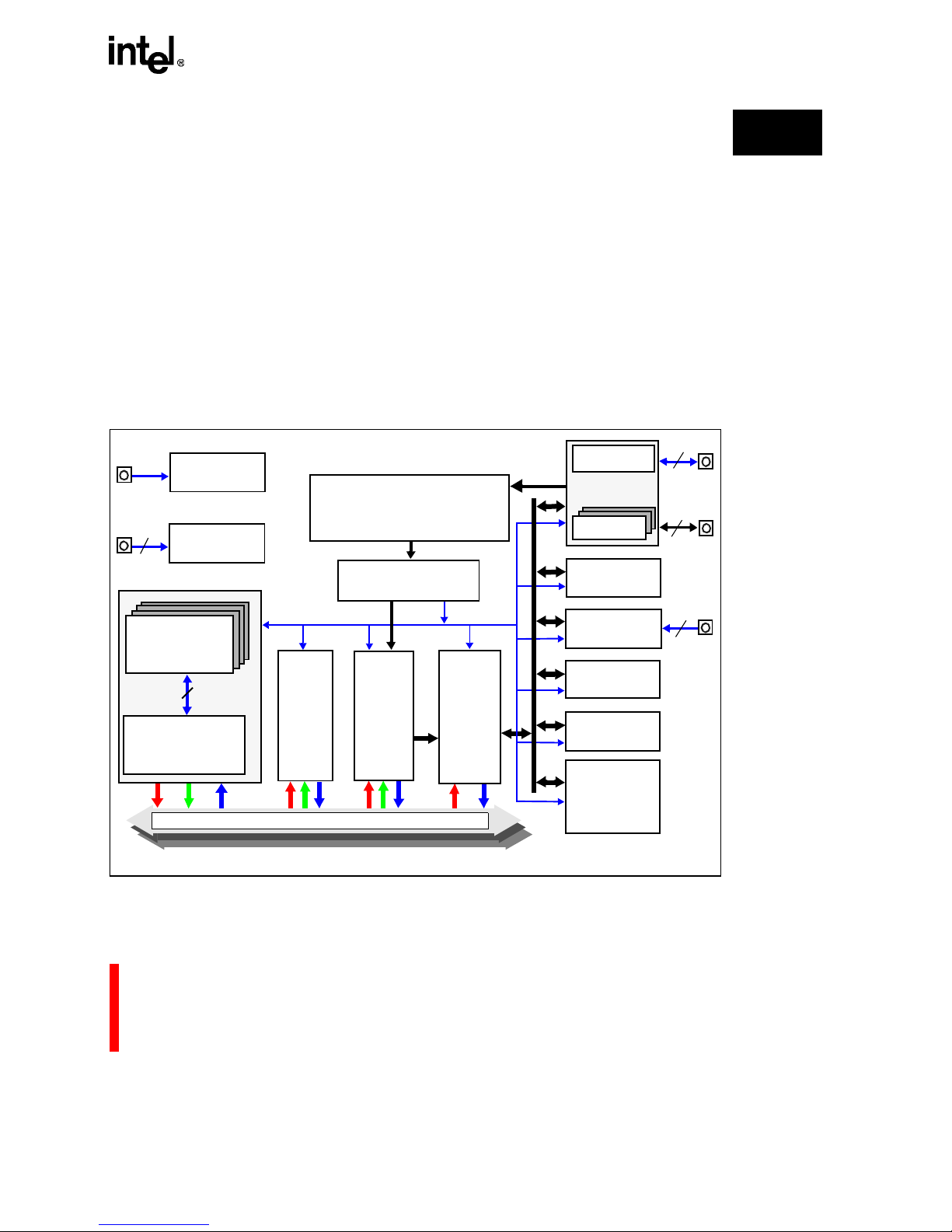
1-3
1
CHAPTER 1
INTRODUCTION
The i960® Jx microprocessor provides a new set of essential enhancements for an emerging class
of high-performance embedded applications. Based on the i960 core architecture, it is
implemented in a proven 0.6 micron, three-layer metal process. Figure 1-1 identifies the
processor’s most notable features, each of which is described in subsections that follow the figure.
These features include:
Figure 1-1. i960® Jx Microprocessor Functional Block Diagram
• instruction cache • data cache • bus controller unit
• on-chip data RAM • local register cac he • interrupt controller
• timer units • memory-mapped control registers • external bus
Programmable
Bus
Control Unit
80960JF, JD: 4 Kbyte
Two-way Set Associative
Interrupt Controller
Control
Address/
Instruction Sequencer
Physical Region
Configuration
Interrupt
Port
1K byte
Data RAM
Instruction Cache
Memory
Interface
Execution
Multiply
Unit
Divide
Unit
Memory Mapped
Register Interface
Data Cache
JF, JD: 2 Kbyte
Direct Mapped
Data Bus
Global / Local
Register File
SRC2 DEST
SRC1
address
Control
effective
Constants
Generation
Unit
Address
32-bit Data
Bus Request
Queues
and
Two 32-Bit
Timers
7-Set
Local Register Cache
SRC1
SRC2
DEST
PLL, Clocks,
Power Mgmt
Boundary Scan
Controller
TAP
5
CLKIN
128
SRC1
SRC2
DEST
SRC1
DEST
9
32
32-bit buses
address / data
21
80960JA: 2 Kbyte
JA: 1 Kbyte
80960JT: 16 Kbyte
JT: 4 Kbyte
32-bit Addr
Three Independent 32-Bit SRC1, SRC2, and DEST Buses
Page 28

INTRODUCTION
1-4
1.1 PRODUCT FEATURES
The i960 Jx processor bring s many enhancements to the i960 microprocessor family, including:
• Improvements to the core architecture
• Low power mode
• New instructions
• Improved cache design
• Enhanced bus control unit
• Improved interrupt performance
• J T A G te s tabilit y
1.1.1 Instruction Cache
The i960 JT p rocessor features a 16 Kbyte two-way set-asso ciative instruction cach e. The i960 JF
and JD processors emplo y a 4-Kb yte, two- w ay set-associ ative in s truction cache. i9 60 JA processors
feature a 2-Kby te instruction cach e. A mecha nism is provid ed that allow s software to lock critical
code within each “w ay” of th e cach e. Th e cach e can be disab led and is m an aged b y us e of th e
icctl
and sysctl instructions, as described in section 4.4, “INSTRUCTION CACHE” (pg. 4-4).
1.1. 2 Data Cache
The i960 JT processor features a 4 Kbyte direct-mapped data cache. The i960 JF and JD
processors feature a 2-Kbyte, direct-mapped data cache that is write-through and write-allocate.
i960 JA processors feature a 1-Kbyte direct-mapped data cache. These processors have a line size
of four words and impleme nt a “natural ” fill policy . Each line in th e cache has a valid bit; to
reduce fetch latency on cache misses, each word within a line also has a valid bit. See section 4.5,
“DATA CACHE” (pg.4-6) for details.
The data cache is managed through the
dcctl instruction; see section 6.2.23, “dcctl ” (pg. 6-40).
1.1.3 On-chip (Internal) Data RAM
The processor’s 1 Kbyte internal data RAM is accessible to software with an access time of
1 cycle per word. This RAM is mapped to the physical address range of 0 to 3FFH. The first
64 bytes are reserved for the caching of dedicated-mode interrupt vectors; this reduces interrupt
latency for these interrupts. In addition, write-protection for the first 64 bytes is provided to guard
against the effects of usi ng null pointers in ‘C’ and to protec t the cached interrupt vectors.
Page 29

INTRODUCTION
1-5
1
The i960 processor compilers can take advantage of the internal data RAM; profiling compilers
can allocate the most frequently used variables into this RAM. See Section 4.1, INTERNAL
DATA RAM (pg. 4-1) for more detail.
1.1.4 Local Register Cache
The processor provides fast storage of local registers for call and return operations by using an
internal local register cache. This cache can store up to seven local register sets; additional register
sets must be saved in external m e mory.
The processor uses a 128-bit wide bus to store local register sets quickly to the register cache. To
reduce interrupt latency for high-priority interrupts, the number of sets that can be used by code
that is running at a lower priority or that is not interrupted can be restricted by programming the
register configuration word in the PRCB. This ensures that there are always sets available for
high-priority interrupt code without needing to save sets in external memory first. See Section 4.2,
LOCAL REGISTER CACHE (pg. 4-2) for more details.
1.1.5 Interrupt Controller
The interrupt controller unit (ICU) provides a flexible, low-latency means for requesting interrupts.
It handles the posting of interrupts requested by hardware and software sources. Acting independently from the core, the interrupt controller compares the priorities of posted interrupts with the
current process priority, off-loading this task from the core. The interrupt controller is compatible
with i960 CA/CF processors .
The interrupt controller provides the following features for handling hardware-requested interrupts:
• Support of up to 240 external sources.
• Eight external interrupt pins, one non-maskable interrupt (NMI
) pin for detection of
hardware-requested interr upts and two internal timer sources.
• Edge or level detection on external interrupt pins.
• Debounce option on externa l interrupt pins.
The application program interfaces to the interrupt controller with six memory-mapped control
registers. The interrupt control register (ICON) and interrupt map control registers
(IMAP0-IMAP2) provide configuration information. The interrupt pending (IPND) register posts
hardware-requested interrupts. The interrupt mask (IMSK) register selectively masks
hardware-requested inter rupts .
The interrupt inputs can be configured to be triggered on level-low or falling-edge signals.
Sampling of the input pins can be either debounced sampling or fast sampling.
Page 30

INTRODUCTION
1-6
The i960 Jx processor has approximately 5 to 10 times faster interrupt servicing than the i960 Kx
processor. This is accomplished through a number of features:
• a hardware priority resolver removes the need to access the external interrupt table to resolve
interrupts
• caching of dedicated-mode interrupt vectors in the internal data RAM
• reserving frames in the local register cache for high -priority interrupts
• the ability to lock the code of interrupt service routines in the instruction-cache reduces the
fetch latency for st arting up these routines
CHAPTER 11, INTERRUPTS discusses this in more detail.
1.1. 6 Timer Supp o rt
The i960 Jx processor provides two identical 32-bit timers. Access to the timers is through
memory-mapped registers. The timers have a single-shot mode and auto-reload capabilities for
continuous operation. Each timer has an independent interrupt request to the i960 Jx processor
interrupt controller. See CHAPTER 10, TIMERS for a complete description.
1.1.7 Memory-Mapped Control Registers (MMR)
Control registers in the i960 Jx pro cessor are memor y- mapped to allow for visibility to application
software. This includes registers for memory configuration, internally cached PRCB data,
breakpoint registers, and interrupt control. These registers are mapped to the architecturally
reserved address space range of FF00 0000H to FFFF FFFFH. The process or ensures that accesses
to the MMRs generate no external bus cycles.
Section 3.3, MEMORY-MAPPED CONTROL REGISTERS (pg. 3-6) discusses this in more
detail.
1.1.8 External Bus
The 32-bit multiplexed external bus connects the i960 Jx processor to memory and I/O. This high
bandwidth bus provides burst transfer capability allowing up to four successive 32-bit data word
transfers at a maximum rate of one word every clock cycle. In addition to the bus signals, the i960
Jx processor provides signals to allow external bus masters. Lastly, the processor provides
variable bus-width support (8-, 16-, and 32-bit).
Page 31

INTRODUCTION
1-7
1
1.1.9 Com pl et e Fault Handling a nd De b ug Capabiliti e s
To aid in program development, the i960 Jx processor detects faults (exceptions). When a fault is
detected, the proces sors make an implicit call to a fault handling routine. Information collected for
each fault allows a program developer to quickly correct faulting code. The processors also allow
automatic recovery from most faults.
To support system debug, the i960 architecture provides a mechanism for monitoring processor
activities through a software tra cing facility. This processor can be configured to detect as many as
seven different trace events, including breakpoints, branches, calls, supervisor calls, returns,
prereturns and the execution of each instruction (for single-stepping through a program). The
processors also provide four breakpoint registers that allow brea k decisions to be made based upon
instruction or da ta addresses.
1.2 ABOUT THIS MANUAL
This i960
®
Jx Microprocessor User’s Manual provides detailed programming and hardware
design information for the i960 Jx microprocessors. It is written for programmers and hardware
designers who understand the basic operating principles of microprocessors and their systems.
This manual does not provide electrical specifications such as DC and AC parametrics, operating
conditions and packaging specifications. Such information is found in the product’s data sheets:
• 80960JA/JF Embedded 32-bit Microprocessor Data Sheet (272504)
• 80960JD Embedded 32-bit Microprocessor Data Sheet (2725 96)
• 80L960JA/JF 3.3 V Embedded 32-bit Microprocessor Data Sheet (272744)
• 80960JA/JF 3.3 V Embedded 32-bit Microprocessor Data Sheet (273146)
• 80960JD 3.3 V Embedded 32-bit Microprocessor Data She et (272971)
• 80960JT 3.3 V Embedded 32-bit Microprocessor Data Sheet (273109)
Each document has a corresponding Specification Update document. These contain the l atest technical
information about the product and documentation, and are available from Intel’s website. For information on
other i960 processor family products or the architecture in general, refer to Intel's Solutions960
®
Development Too ls Catalog (270791). It lists all current i 960 microprocessor family-related do cuments,
support components, boards, software development tools, debug tools and more.
This manual is organized in three parts; each part comprises multiple chapters and/or appendices.
The following briefly describes each part:
• Part I - Programming the i960 Jx Microprocessor (chapters 2-10) details the programming
environment for the i960 Jx devices. Described here are the processor's registers, instruction set, data
types, addressing modes , interrupt m echanism, external interrupt interfac e and fault m echanism.
Page 32

INTRODUCTION
1-8
• Part II - System Implementation (chapters 11-17) identifies requirements for designing a system
around the i96 0 Jx components, such a s external bus interface and in terrupt controller. Also
described are programming requirements for the bus controller and processor initialization.
• Part III - Appendices includes quick references for hardware design and programming.
Appendices are also provided which describe the internal architecture, how to write
assembly-level code to exploit the parallelism of the processor and considerations for writing
software that is portable among all members of the i960 micr oprocessor family.
1.3 NOTATION AND TERMINOLOGY
This section def ines terminology and textual conventions that are used throughout the manual.
1.3.1 Reserved and Preserved
Certain fields in reg isters and data structures are described as being either reserved or preserved:
• A reserved field is one that may be used by other i960 architecture implementations. Correct
treatment of reserved fields ensures software compatibility with other i960 processors. The
processor uses these fields for temporary storage; as a result, the fields sometimes contain
unusual values.
• A preserved field is one that the processor does not use. Software may use preserved fields for
any function.
Reserved fields in certain data structures should be cleared (set to zero) when the data structure is
created. Clear the reserved fields when creating the Interrupt Table, Fault Table and System
Procedure Table. Software should not modify or rely on these reserved field values after a data
structure is created. When the processor creates the Interrupt or Fault Record data structure on the
stack, software should not depend on the value of the reserv ed fields within these data structures.
Some bits or fields in data structures and registe r s are shown as requiring specific e ncoding. These
fields should be treated as if they were reserved fields. They should be set to the specified value
when the data structure is created or when the register is initialized and software should not
modify or rely on the value after that.
Reserved bits in the Arithmetic Controls (AC) register can be cleared after initialization to ensure
compatibility with other i960 processor implementations. Reserved bits in the Process Controls
(PC) register and Trace Controls (TC) regis ter should not be initialized. When the AC, PC and TC
registers are modified using
modac, modpc or modtc instructions, the reserved loc ations in thes e
registers must be masked.
Page 33

INTRODUCTION
1-9
1
Certain areas of memory may be referred to as reserved memory in this reference manual.
Reserved — when referring to memory locations — implies that an implementation of the i960
architecture may use this memory for some special purpose. For example, memory-mapped
peripherals might be located in reserved memory areas on future implementations.
1.3.2 Specifying Bit and Signal Values
The terms set and clear in this manual refer to bit values in register and data structures. When a bit
is set, its value is 1; when the bit is clear, its value is 0. Likewise, setting a bit means giving it a
value of 1 and clearing a bit means giving it a value of 0.
The terms assert and deassert refer to the logically active or inactive value of a signal or bit,
respectively. A signal is specified as an active 0 signal by an overbar. For example, the input is
active low and is asse rted by driving the signal to a logic 0 value.
1.3.3 Representing Numbers
All numbers in this manual can be assumed to be base 10 unless designated otherwise. In text,
binary numbers are sometimes designated with a subscript 2 (for example, 001
2
). When it is
obvious from the context that a number is a binary numbe r, the “2” subscript may be omitted.
Hexadecimal numbers are de signated in text with the suffix H (for example, FFFF FF5AH). In
pseudo-code action statements in the instruction reference section and occasionally in text,
hexadecimal numbers are represented by adding the C-language convention “0x” as a prefix. For
example “FF7AH” appears as “0x FF7A” in the pseudo-code.
1.3.4 Register Names
Memory-mapped registers and several of the global and local registers are referred to by their
generic register names, as well as descriptive names which describe their function. The global
register numbers are g0 through g15; local register numbers are r0 through r15. However, when
programming the registers in user-generated code, make sure to use the instruction operand. i960
microprocessor compilers recognize only the instruction operands listed in Table 1-1. Throughout
this manual, the registers’ descriptive names, numbers, operands and acronyms are used interchangeab ly, as dictated by context.
Groups of bits and single bits in registers and control words are called either bits, flags or fields.
These terms have a dist inct meaning in this manua l:
bit Controls a processor func tion; programmed by the user.
flag Indicates status. Generally set by the processor; certain flags are user programmable.
field A grouping of bits (bit field) or flags (flag field).
Page 34

INTRODUCTION
1-10
Specific bits, flags and fields in registers and control words are usually referred to by a register
abbreviation (in upper case) followed by a bit, flag or field name (in lower case). These items are
separated with a period. A position number designates individual bits in a field. For example, the
return type (rt) field in the previous frame pointer (PFP) register is designated as “PF P.rt”. The
least significant bit of the return type field is then designated as “PFP.rt0”.
1.4 RELATED DOCUMENTS
The following documents are useful when designing with and programming the i960 microprocessor. Check the Intel website or contact your local sales representative for more information on
obtaining Intel documents, including Specification Updates.
• 80960JA/JF Embedded 32-bit Microprocessor Data Sheet (272504)
• 80960JD Embedded 32-bit Microprocessor Data Sheet (2725 96)
• 80L960JA/JF 3.3 V Embedded 32-bit Microprocessor Data Sheet (272744)
• 80960JA/JF 3.3 V Embedded 32-bit Microprocessor Data Sheet (273146)
• 80960JD 3.3 V Embedded 32-bit Microprocessor Data She et (272971)
• 80960JT 3.3 V Embedded 32-bit Microprocessor Data Sheet (273109)
• Solutions960
®
Development Tools Catalog (270791)
Table 1-1. Register Termi nology Conventions
Register Descriptive Name Register Number Instruction Operand Acronym
Global Registers g0 - g15 g0 - g14
Frame Pointer
g15 fp FP
Local Registers r0 - r15 r3 - r15
Previous Frame Pointer
r0 pfp PFP
Stack Pointer
r1 sp SP
Return Instruction Pointer
r2 rip RIP
Page 35

2
DATA TYPES AND MEMORY
ADDRESSING MODES
Page 36

Page 37
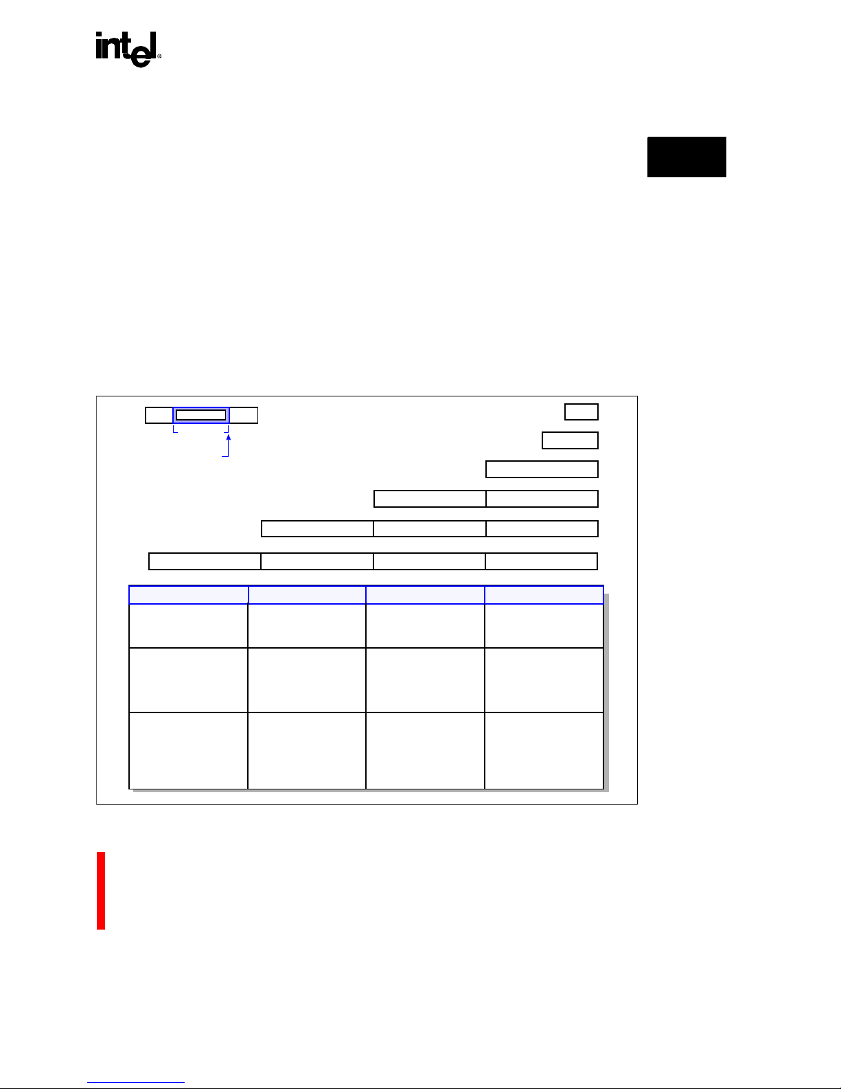
2-1
2
CHAPTER 2
DATA TYPES AND MEMORY ADDRESS ING MODES
2.1 DATA TYPES
The instruction set references or produces several data lengths and formats. The i960
®
Jx
processor supports the following data types:
Figure 2-1 illustrates the class, data type and length of each type supported by i960 processors.
Figure 2-1. Data Types and Ranges
• Integer (signed 8, 16 and 32 bits) • Ordinal (unsigned integer 8, 16, 32 and 64 bits)
• Long-Word (64 bits) • Triple-Word (96 bits)
• Quad-Word (128 bits) • Bit Field
•Bit
Byte
Short
Word
Triple-Word
Quad-Word
8
Bits
16
Bits
32
Bits
64
Bits
96
Bits
128
Bits
Numeric
(Integer)
Numeric
(Ordinal)
Non-Numeric
Byte Integer
Short Integer
Integer
Byte Ordinal
Short Ordinal
Ordinal
Bit
Bit Field
Triple-Word
Quad-Word
8 Bits
16 Bits
32 Bits
8 Bits
16 Bits
32 Bits
1 Bit
1-32 Bits
96 Bits
128 Bits
-2
7
to 27 -1
-2
15
to 215 -1
-2
31
to 231 -1
0 to 2
8
-1
0 to 2
16
-1
0 to 2
32
-1
N/A
Bit Field
Length
LSB of
Bit Field
0
0
0
0
7
15
31
63
Class Data Type Length Range
0
0
95
127
0
31
Long-Word
64 Bits
Long
Long Ordinal 64 Bits 0 to 2
64
- 1
Page 38

DATA TYPES AND MEMORY ADDRESSING MODES
2-2
2.1.1 Integers
Integers are signed whole num bers that are stored and operated on in two’s complement format by
the integer in st ruct ion s. Mos t integ er i ns tructio ns op erate on 32-bit inte gers. Byte and shor t int e ger s
are referenced by the byte and short classes of the load, store and compare instructions only.
Integer load or store size (byte, short or word) determines how sign extension or data truncation is
performed when data is moved between registers and memory.
For instructions
ldib (load integer byte) and ldis (load integer short), a byte or short word in
memory is considered a two’s complement value. The value is sign-extended and placed in the
32-bit regis ter that is the destination for the load.
Example 2-1. Sign Extensions on Load Byte and Load Short
For instructions stib (store integer byte) and stis (store integer short), a 32-bit two’s complement
number in a register is stored to memory as a byte or short word. When registe r data is too large to
be stored as a byte or short word, the value is truncated and the integer overflow condition is
signalled. When an overflow occurs, either an AC register flag is set or the ARITHMETIC.INTEGER_OVERFLOW fault is generated, depending on the Integer Overflow Mask bit
(AC.om) in the AC register. CHAPTER 8, FAULTS describes the integer overflow fault.
For instructions
ld (load word) and st (store word), data is moved directly between memory and a
register with no sign extension or data truncati on.
2.1.2 Ordinals
Ordinals or unsigned integer data types a r e stored and treated as positive binary values. Figure 2-1
shows the supported ordinal sizes.
The large number of instructions that perform logical, bit manipulation and unsigned arithmetic
operations refere nce 32-bit ordinal operands. When ordinals are used to represent Bool ean values,
1 = TRUE and 0 = FALSE. Most extended arithmetic instructions reference the long ordinal data
type. Only load (
ldob and ldos), store (stob a nd stos), and compar e or dina l inst r uct ion s refe ren ce
the byte and short ordinal data types.
ldib
7AH is loaded into a register as 0000 007AH
FAH is loaded into a register as FFFF FFFAH
ldis
05A5H is loaded into a register as 0000 05A5H
85A5H is loaded into a register as FFFF 85A5H
Page 39

DATA TYPES AND MEMORY ADDRESSING MODES
2-3
2
Sign and sign extension are not considered when ordinal load s and stores are performed; the values
may, however, be zero-extended or truncated. A short word or byte load to a register causes the
value loaded to be zero-extended to 32 bits. A short word or byte store to memory truncates an
ordinal value in a register to fit the size of the destination memory. No overflow condition is
signalled in this case.
2.1.3 Bits and Bit Fields
The processor provides several instructions that perform operations on individual bits or bit fields
within register operands. An individual bit is specified for a bit operation by giving its bit number
and register. Internal registers always follow little endian byte order; the least significant bit
corresponds to bit 0 and the most significant bit corresponds to bit 31.
A bit field is any contiguous group of bits (up to 32 bits long) in a 32-bit register. Bit fields do not
span register boundaries. A bit field is defined by giving its length in bits (1-32) a nd the bit number
of its lowest numbered bit (0-31).
Loading and storing bit and bit-field data is normally performed using the ordinal load (
ldo) and
store (
sto) instructions. When an ldi instruction loads a bit or bit field value into a 32-bit register,
the processor appends sign extension bits. A byte or short store can signal an integer overflow
condition.
2.1.4 Triple- and Quad-Words
Triple- and quad-words refer to consecutive words in memory or in registers. Triple- and
quad-word load, store and move instructions use these data types to accomplish block movements.
No data manipulation (sign extension, zero extension or truncation) is performed in these instructions.
Triple- and quad-word data types can be considered a superset of the other data types described.
The data in each word subset of a quad-word is likely to be the operand or result of an ordinal,
integer, bit or bit field instruction.
2.1.5 Register Data Alignment
Several of the processor’s instructions operate on multiple-word operands. For example, the
load-long instruction (
ldl) loads two words from memory into two consecutive registers. The least
significant data word is loaded into the lower order register. The most significant data word is
loaded into the high er order register.
Page 40

DATA TYPES AND MEMORY ADDRESSING MODES
2-4
In cases where an instruction specifies a register number (and multiple, consecutive registers are
implied), the register number must be even when two registers are accessed (e.g., g0, g2) and an
integral multiple of four when three or four registers are accessed (e.g., g0, g4). When a register
reference for a source value is not properly aligned, the registers that the processor writes to are
undefined.
The i960 Jx processor does not require data alignment in external memory; th e processor hardware
handles unaligned memory accesses automatically. Optionally, user software can configure the
processor to generate a fault on unaligned memory accesses.
2.1.6 Literals
The architecture defines a set of 32 literals that can be used as operands in many instructions.
These literals are ordinal (unsigned) values that range from 0 to 31 (5 bits). When a literal is used
as an operand, the processor expands it to 32 bits by adding leading zeros. When the instruction
requires an operand larger than 32 bits, the processor zero-extends the value to the operand size.
When a literal is used in an instruction that requires integer operands, the processor treats the
literal as a positive in teger valu e.
2.2 BIT AND BYTE ORDERING IN MEMORY
All occurrences of numeric and non-numeric data types, except bits and bit fields, must start on a
byte boundary. Any data item occupying multiple bytes is stored as big e ndian or littl e e ndian. The
following sections further describe byte ordering .
2.2.1 Bit Ordering
Bits within bytes are numbered such that when the byte is viewed as a value, bit 0 is the least
significant bit and bit 7 is the most significant bit. For numeric values spanning several bytes, bit
numbers higher than 7 indicate successively higher bit numbers in bytes with higher addresses.
Unless otherwise noted, bits in illustrations in this manual are ordered such that the
higher-numbered bits are to the left.
2.2. 2 Byte Ordering
The i960 Jx processor can be programmed to use little or big endian byte ordering for memory
accesses. Byte ordering refers to how data items larger than one byte are assembled:
• For little endian byte order, the byte with the lowest address in a multi-byte data item has the
least significance.
• For big endian byte order, the byte with the lowest address in a multi-byte data item has the
most significance.
Page 41

DATA TYPES AND MEMORY ADDRESSING MODES
2-5
2
For ex ample, Table 2-1 shows eight bytes of data in memory. Table 2-2 shows the differences
between little and big endian accesses for byte, short, word and long-word data. Figure 2-2 shows
the resu ltant da ta pl ac ement in r eg isters.
Once data is read into registers, byte order is no longer relevant. The lowest significant bit is
always bit 0. The most significant bit is always bit 31 for words, bit 15 for short words, and bit 7
for bytes.
Byte ordering affects the way the i960 Jx processor handles bus accesses. See section 13.6.2,
“Selecting the Byte Order” (pg. 13-12) for more information.
Table 2-1. Memory Contents for Little and Big Endian Example
ADDRESS DATA
1000H 12H
1001H 34H
1002H 56H
1003H 78H
1004H 9AH
1005H BCH
1006H DEH
1007H F0H
Table 2-2. Byte Ordering for Little and Big Endian Accesses
Access Example
Register Contents
(Little Endian)
Register Content s
(Big Endian)
Byte at 1000H ldob 0x1000, r3 12H 12H
Short at 1002H ldos 0x1002, r3 7856H 5678H
Word at 1000H ld 0x1000, r3 78563412H 12345678H
Long-Word at 1000H ldl 0x1000, r4
78563412H (r4)
F0DEBC9AH (r5)
12345 678 H (r 4)
9ABCD EF0 H (r 5)
Page 42

DATA TYPES AND MEMORY ADDRESSING MODES
2-6
Figure 2-2. Data Placement in Registers
2.3 MEMORY ADDRESSING MODES
The processor provides nine modes for addressing operands in memory. Each addressing mode is used
to reference a byte location in th e p r o cess o r’s address space. Table 2-3 shows the memory addressing
modes and a brief descri ption of each mode’s address elements and assembly code syntax.
Table 2-3. Memory Addressing Modes
Mode Description Assembler Syntax
Inst.
Type
Absolute
offset
offset (smaller than 4096) exp MEMA
displacement
displacement (larger than 4095) exp MEMB
Register Indirect abase (reg) MEMB
with offset
abase + offset exp (reg) MEMA
with displacement
abase + displacement exp (reg) MEMB
with index
abase + (index*scale) (reg) [reg*scale] MEMB
with index and displacement
abase + (index*scale) +
displacement
exp (reg)
[reg*scale]
MEMB
Index with displacement (index*scal e) + displacement exp [reg*scale] MEMB
instruction pointer (IP) with
displacement
IP + displacement + 8 exp (I P) MEMB
NOTE:
reg
is register,
exp
is an expression or symbolic label, and IP is th e Instruction Pointer.
Byte
Short
Word
XX XX XX DD
0
XX XX DD
1
DD
0
DD
3
DD
2
DD
1
DD
0
08 716 1524 2331
08 716 1524 2331
08 716 1524 2331
NOTES:
D’s are data transferred to/from memory
X’s are zeros for ordinal data
X’s are sign bit extensions for integer data
Page 43

DATA TYPES AND MEMORY ADDRESSING MODES
2-7
2
See Table B-9 in APPENDIX B for more on addressing modes. For purposes of this memory
addressing modes description, MEMA format instructions require one word of memory and
MEMB usually require two words and therefore consume twice the bus bandwidth to read.
Otherwise, both forma ts perform the same functions.
2.3.1 Absolute
Absolute addressing modes allow a memory location to be referenced directly as an offset from
address 0H. At the instruction encoding level, two absolute addressing modes are provided:
absolute offset and absolute displacement, depending on offset size.
• For the absolute offset addressing mode, the offset is an ordinal number ranging from 0 to 4095.
The absolute offset addressing mode is encoded in the MEMA machine instruction format.
• For the absolute displacement addressing mode, the offset value ranges from 0 to 2
32
-1. The
absolute displa ce ment addressing mode is encode d in the MEMB format.
Addressing modes and encoding instruction formats are described in CHAPTER 6,
INSTRUCTION SET REFERENCE.
At the assembly langua ge leve l, the two ab solut e addr essing mode s use the sa me synta x. Typic ally,
development tools allow absolute addresses to be specified through arithmetic expressions
(e.g., x + 44) or symbolic labels. After evaluating an address specified with the absolute a ddressing
mode, the assembler converts the addre ss into an offset or displacement and selects the appr opriate
instruction e ncoding format and addressing mode.
2.3.2 Register Indirect
Register indirect addressing modes use a register’s 32-bit value as a base for address calculation.
The register value is referred to as the address base (designated “abase” in Table 2-3). Depending
on the addressing mode, an optional scaled index and offset can be added to this address base.
Register indirect addressing modes are useful for addressing elements of an array or record
structure. When addressing array elements, the abase value provides the address of the first array
element. An offset (or displacement) selects a particular ar ray element.
In register-indirect-with-index addressing mode, the ind ex is specified using a value contained in a
register. This i nde x value is multi pl ied by a scal e factor. All owable fa ctors a re 1, 2, 4, 8 and 16. The
register-indirect-with-index addressing mode is encoded in the MEMB format.
The two versions of register-indirect-with-offset addressing mode at the instruction encoding level
are register-indirect-with-offset and register-indirect-with-displacement. As with absolute
addressing modes, the mode selected depends on the si ze of the offset from the base address.
Page 44

DATA TYPES AND MEMORY ADDRESSING MODES
2-8
At the assem b ly langua g e level, th e assem b ler allo w s th e offset to b e sp ecified w it h an expr e s sion
or symbolic label, then evaluates the address to determine whether to use register-indirect-withoffset (MEMA format) or register-indirect-with-displacement (MEMB format) addressing mode.
Register-indirect-with-index-and-displacement addressing mode adds both a scaled index and a
displacement to the address base. There is only one version of this addressing mode at the
instruct ion encoding level, and it is encoded in the MEMB instruction for ma t.
2.3.3 Index with Displacement
A scaled index can also be used with a displacement a lone. The index is contained in a register and
multiplied by a scaling constant before displ acement is added. This mode uses MEMB format .
2.3.4 IP with Displacement
This addressing mode is used with load and store instructions to make them instruction pointer
(IP) relative. IP-with-displacement addressing mode references the next instruction’s address plus
the displacement. This mode uses MEMB format.
2.3.5 Addressing Mode Example s
The following examples show how i960 processor addressing modes are encoded in assembly
language. Exa mple 2-2 shows addressing mode mnemonics. Example 2-3 illustrates the
usefulness of scaled index and scaled index plus displacement addressing modes. In this example,
a procedure named array_op uses these addressing modes to fill two contiguous memory blocks
separated by a constant offset. A point er to the t op of the bloc k is pass ed to the procedure in g0, the
block size is pass ed in g1 and the fill data in g2.
For more details on encoding formats, refer to APPENDIX C, MACHINE-LEVEL
INSTRUCTION FORMATS.
Page 45

DATA TYPES AND MEMORY ADDRESSING MODES
2-9
2
Example 2-2. Addressing Mode Mnemonics
Example 2-3. Scaled Index and Scaled Index Plus Displacement Addressing Modes
st g4,xyz # Absolute; word from g4 stored at memory
# location designated with label xyz.
ldob (r3),r4 # Register indirect; ordinal byte from
# memory location given in r3 loaded
# into register r4 and zero extended.
stl g6,xyz(g5) # Register indirect with displacement;
# double word from g6,g7 stored at memory
# location xyz + g5.
ldq (r8)[r9*4],r4 # Register indirect with index; quad-word
# beginning at memory location r8 + (r9
# scaled by 4) loaded into r4 through r7.
st g3,xyz(g4)[g5*2] # Register indirect with index and
# displacement; word in g3 stored to mem
# location g4 + xyz + (g5 scaled by 2).
ldis xyz[r12*2],r13 # Index with displacement; load short
# integer at memory location xyz + r12
# into r13 and sign extended.
st r4,xyz(ip) # ip with displacement; store word in r4
# at memory location IP + xyz + 8.
array_op:
mov g0,r4 # Pointer to array is copied to r4.
subi 1,g1,r3 # Calculate index for the last array
b .I33 # element to be filled
.I34:
st g2,(r4)[r3*4] # Fill element at index
st g2,0x30(r4)[r3*4] # Fill element at index+constant offset
subi 1,r3,r3 # Decrement index
.I33:
cmpible 0,r3,.I34 # Store next array elements if
ret # index is not 0
Page 46

Page 47

3
PROGRAMMING
ENVIRONMENT
Page 48

Page 49

3-1
3
CHAPTER 3
PROGRAMMING ENVIRONMENT
This chapter describes the i960® Jx processor’s programming environment including global and
local registers, control registers, literals, processor-state registers and address space.
3.1 OVERVIEW
The i960 architecture defines a programming environment for program execution, data storage and data
manipulation. Figure 3-1 shows the programming environment elements that include the following:
The processor include s several architecturally-defined data structures located in memory as part of
the programming environment. These data structures handle procedure calls, interrupts and faults
and provide configuration information at initialization. These da ta s tructures are:
3.2 REGISTERS AND LITERALS AS INSTRUCTION OPERANDS
With the exception of a few special instructions, the i960 Jx processor uses load and store instructions to access memory. All operat io ns take pla ce at th e registe r level . The proces sor use s 16 global
registers, 16local registers and 32 literals (constants 0-31) as instruction operands.
The global register numbers are g0 through g15; loc al register numbers are r0 thro ugh r15. Several
of these registers are used for dedicated functions. For example, register r0 is the previous frame
pointer, often referred to as pfp. The i960 processor compilers and assemblers recognize only the
instruction operands listed in Table 3-1. T hroughout this manual, the registers’ descriptive names,
numbers, operands and acronyms are used interchangeably, as dictated by context .
•4Gbyte (2
32
byte) flat address space • register cache
• instruction cache • set of literals
• data cac h e • control registers
• global and local general-purpose registers • set of processor state registers
• interrupt stack • control table • system procedure table
• local stack • fault table • process control block
• supervisor stack • interrupt table • initialization boot record
Page 50
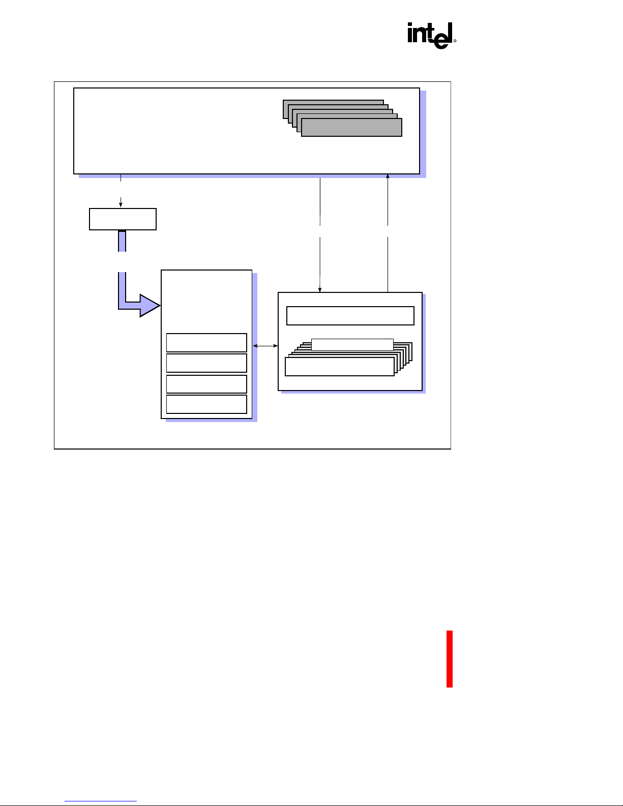
PROGRAMMING ENVIRONMENT
3-2
Figure 3-1. i960® Jx Processor Programming Envi ronment Elements
3.2.1 Global Registers
Global registers are general-purpose 32-bit data registers that provide temporary storage for a
program’s computational operands. These registers retain their contents across procedure
boundaries. They provide a fast and efficient means of passing parameters between procedures.
Architecturally
Defined
Data Structures
FFFF FFFFH
Instruction
Stream
Instruction
Execution
Processor State
Registers
Instruction
Pointer
Arithmetic
Controls
Process
Controls
Trace
Controls
Address Space
Sixteen 32-Bit
Global Registers
Sixteen 32-Bit
Local Registers
g0
g15
r0
r15
Load
Store
0000 0000H
Register Cache
Fetch
Instruction
Cache
r15
Page 51
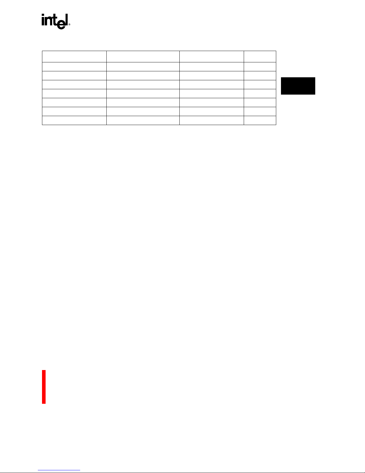
PROGRAMMING ENVIRONMENT
3-3
3
The i960 architecture supplies 16 global registers, designated g0 through g15. Register g15 is
reserved for the current Frame Pointer (FP), which contains the address of the first byte in the
current (topmost) stack frame in memory. See CHAPTER 7, PROCEDURE CALLS for a
description of the FP and pr ocedure stack.
After the processor is reset, register g0 contains device identification and stepping information
(DeviceID). Refer to Section 1.4, ”Related Documents” (pg. 1-10). Further information on Device
IDs can be found in these documents. The information is retained in g0 until it is written over by
the user program. The device identification and stepping information is also stored in the
memory-mapped DEVICEID register located at FF00 8710H.
3.2.2 Local Registers
The i960 architecture provides a separate set of 32-bit local data regis ters (r0 through r15) for each
acti ve pr oce dure . T hese re gist ers prov ide sto rage fo r v ariab les that a re lo cal to a pr oc edur e. Ea ch
time a procedure is called, the processor allocates a new set of local registers and saves the calling
procedure’s loca l registers. When the application returns from the procedure, the local registers are
released for the next procedure call. The processor performs local register management; a program
need not explicitly save and restore these registers.
Local registers r3 through r15 are general purpose registers; r0 through r2 are reserved for special
functions; r0 contains the Pre vious Fra me Pointer (PFP); r1 contains the Stack Pointer (SP); r2 cont ains
the Return Instruction Pointer (RIP). These are discussed in CHAPTER 7, PROCEDURE CALLS.
The processor does not always clear or initialize the set of local registers assigned to a new
procedure. Also, the processor does not initialize the local register save area in the newly created
stack frame for the procedure. User software should not rely on the initial values of local registers.
Table 3-1. Registers and Lite rals Used as Instruction Operands
Instruction Operand Register Name (number) Function Acronym
g0 - g14 global (g0-g14) general purpose
fp global (g15) frame pointer FP
pfp local (r0) previous frame point er PFP
sp local (r1) stack poi nt er SP
rip local (r2) return instruc ti on pointer RIP
r3 - r15 local (r3-r15) general purpose
0-31 literals
Page 52

PROGRAMMING ENVIRONMENT
3-4
3.2.3 Register Scoreboarding
Register scoreboarding maintains register coherency by preventing parallel execution units from
accessing registers for which there is an outstanding operation. When an instruction that targets a
destination register or group of registers executes, the processor sets a register-scoreboard bit to
indicate that this register or group of register s is being used in an operation. When the instructions
that follow do not require data from registers already in use, the processor can execute those
instructions be fore the prior instruction completes execution.
Software can use this feature to execute one or more single-cycle instructions concurrently with a
mult i-c ycl e inst ru ctio n ( e.g. , mu lti ply o r di vid e). Example3-1 shows a case wher e register scor e-
boarding prevents a subsequent instruction from executing. It also illustrates overlapping instructions that do not have register dependencies.
Example 3-1. Register Scoreboarding
3.2.4 Literals
The architecture defines a set of 32 literals that can be used as operands in many instructions.
These literals are ordinal (unsigned) values that range from 0 to 31 (5 bits). When a literal is used
as an operand, the processor expands it to 32 bits by adding leading zeros. When the instruction
requires an operand larger than 32 bits, the processor zero-extends the value to the operand size.
When a literal is used in an instruction that requires integer operands, the processor treats the
literal as a positive in teger valu e.
3.2.5 Register and Literal Addressing and Alignmen t
Several instructions operate on multiple-word operands. For example, the load long instruction
(
ldl) loads two words from memory into two consecutive registers. The register for the less
significant word is specified in the instruction. The more significant word is automatically loaded
into the next higher-numbered register.
muli r4,r5,r6 # r6 is scoreboarded
addi r6,r7,r8 # addi must wait for the previous multiply
. # to complete
.
.
muli r4,r5,r10 # r10 is scoreboard ed
and r6,r7,r8 # and instruction is executed concurrently with multiply
Page 53

PROGRAMMING ENVIRONMENT
3-5
3
In cases wh ere an instruction spec ifies a register number a nd multiple consecuti ve registers are
implied, the register number must be even when two registers are accessed (e.g., g0, g2) and an
integral multiple of 4, when 3 or 4 registers are accessed (e.g., g0, g4). When a register reference
for a source value is not properly aligned, the source value is undefined and an
OPERATION.INVALID_OPERAND fault is generated. When a register reference for a
destination value is not properly aligned, the registers to which the processor writes and the values
written are un defined . The proc essor t hen ge nerate s an OPERATION.INVALID_OPERAND faul t.
The assembly language code in Example3-2 shows an example o f correct and incorr ect regist er
alignment.
Example 3-2. Register Alignment
Global registers, local reg is ters and litera ls are used directly as instruction operan ds. Table 3-2 lists
instruction operands for each machine-level instruction format and the positions that can be filled
by each register or literal.
movl g3,g8 # Incorrect alignment - resulting value
. # in registers g8 and g9 is
. # unpredictable (non-aligned source)
.
movl g4, g8 # Co rrect alig nme nt
Table 3-2. Allowable Register Operands
Operand (1)
Instruction
Encoding
Operand Field Local Register
Global
Register
Literal
REG
src1
src2
src/dst
(as
src
)
src/dst
(as
dst
)
src/dst
(as both)
X
X
X
X
X
X
X
X
X
X
X
X
MEM
src/dst
abase
index
X
X
X
X
X
X
COBR
src1
src2
dst
X
X
X (2)
X
X
X (2)
X
NOTES:
1. 1.“X” denotes the register can be used as an operand in a particular instruction field.
2. The
COBR destination operands apply only to TEST instructions.
Page 54

PROGRAMMING ENVIRONMENT
3-6
3.3 MEMORY-MAPPED C ONT R OL REGISTERS
The i960 Jx processor gives software the interface to easily read and modify internal control
registers. Each of these registers is accessed as a 32-bit memory-mapped register (MMR) with a
unique me mory addre ss. The pr ocessor ensur es that acce sses to MM Rs do no t generate e xternal
bus cycl e s .
3.3.1 Memory-Mapped Registers (MMR)
Portions of the i960 Jx processor address space (addresses FF00 0000H through FFFF FFFFH) are
reserved for memory-mapped registers (see section 12.3, “Architecturally Reserved Memory
Space” (pg. 12-9). These memory-mapped registers (MMRs) are accessed through word-operand
memory instructions (
ld and st instructions) and some register class instructions (atmod, atadd
and sysctl). Acce sses to t h e MMRs d o n o t g e n er at e ex ternal b u s cycles . The lat e nc y i n accessi ng
each of these registers is one cycle for
ld and st and multiple cycle s for others.
Each register has an associated access mode (user and supervisor modes) and access type (read
and write accesses). Table 3-4 and Table 3-5 show all the memory-mapped registers and the
application modes of acce ss.
The registers are partitioned into user and supervisor spaces based on their addresses. Addresses
FF00 0000H through FF00 7FFFH are allocated to user space memory-mapped registers;
Addresses FF00 8000H to FFFF FFFFH are allocated to supervisor space registers.
3.3.1.1 Restrictions on Instructions that Access Memory-Mapp ed Registers
The majority of memor y-mapped registers can be accessed by both load (
ld) and store (st) in st ruc-
tions. However some registers have restri ctions on the types of access they allow. To ensure correct
operation, the access type restrictions for each register should be followed. The access type
columns of Table 3-4 and Table 3-5 indicate the allowed access types for each register.
Unless otherwise indicated by its access type, the modification of a memory-mapped register by a
st instruction takes effect completely before the next instruction starts execution.
Some operations require an atomic-read-modify-write sequence to a register, most notably IPND
and IMSK. The
atmod and atadd instructions provide a special mechanism to quickly modify the
IPND and IMSK registers in an atomic manner on the i960 Jx processor. Do not use these
instruction on any othe r me mory -mapped registers.
The
sysctl instruction can also modify the contents of a memory-mapped register atomically; in
addition,
sysctl is the only method to read the breakpoint registers on the i960 Jx processor; the
breakpoints cannot be rea d using a
ld inst r uc tion.
Page 55

PROGRAMMING ENVIRONMENT
3-7
3
At initia lization, the control table automa tically l o ads into the on-chip control registers. This action
simplifies the user’s start-up code by providing a transparent setup of the processor’s peripherals.
See CHAPTER 12, INITIALIZATION AND SYSTEM REQUIREMENTS.
3.3.1.2 Access Faults
Memory-mapped registers are meant to be accessed only as aligned, word-size registers with
adherence to the appropriate access mode. Accessing these registers in any other way results in
faults or undefined operation. An access is performe d usi ng the following fault model:
1. The access must be a word-sized, word-aligned access; otherwise, the processor generates an
OPERATION.UNIMPLEMENTED fault.
2. When the access is a store in user mode to an implemented supervisor location, a
TYPE.MISMATCH fault occurs. It is unpredictable whether a store to an unimplemented
supervisor loca tion causes a fault.
3. When the a ccess is neith er of th e above, t he acc ess is at tempted . Note t hat an MM R may
generate faults based on conditions specific to that MMR. (Example: trying to write the
timer register s in user mode when they have been allocated to supervisor mode only.)
4. When a store access to an MMR faults, the processor ensures that the store does not take effect.
5. A load access of a reserved location returns an unpredictable value.
6. Avoid any store access es to res erved lo catio ns. Suc h a stor e can re sult i n undefin ed op erati on
of the pr o cessor wh en th e location is in superv iso r s p ace.
Instruction fetches from the memory-mapped register space are not allowed and result in an
OPERATION.UNIMPLEMENTED fault.
Page 56
PROGRAMMING ENVIRONMENT
3-8
Table 3-3. Access Types
Access Type Description
R Read Read (ld instruction) accesses are allowed.
RO
Read
Only
Only Read (ld instruction) accesses are allowed. Write (st
instructi on) accesses are ignored.
WWriteWrite (st instructi on) accesses allowed.
R/W Read/Write ld, st, and sysctl instruc ti ons are allowed access.
WwG
Write
when
Granted
Writing or Modifying (through a st or sysctl instruction) the register
is only allowed when modifi cation-rights to the register have been
granted. An OPERATION.UNIMPLEMENTED fa ult occurs when an
attempt is made to write the register before rights are granted. See
section 9.2.7.2, “Hardw are Breakpoints” (pg. 9-5) for details about
getting modification rights to breakpo int registers.
Sysctl-RwG
sysctl
Read
when
Granted
The value of the register can only be read by executing a sysctl
instruction issued with the modify memory-mapped register
message type. Modification rights to the register must be granted
first or an OPERATION.UNIMPLEMENTED fault occurs when the
sysctl is executed . A ld instruct ion to the register ret urns unpre-
dictable results.
AtMod
atmod
update
Register can be updat ed quickl y thro ugh the atmod instruction. The
atmod ensures correct operation by performing the update of the
register in an atomic manner which provides synchronization with
previous and subsequent operations. This is a fast er update
mechanism than sysctl and is optimized for a few specia l registers.
Page 57

PROGRAMMING ENVIRONMENT
3-9
3
Table 3-4. Supervis or Space Fam ily Registers (Sheet 1 of 2)
Register Name
Memory-Mapped
Address
Access Type
Reserved
FF00 8000H to
FF00 80FFH
—
(DLMCON) Default Logical Memory Configuration
Register
FF00 8100H R/W
Reserved
FF00 8104H —
(LMADR0) Logical Memory Address Register 0 FF00 8108H R/W
(LMMR0) Logical Memory Mask Regi ster 0 FF00 810CH R/W
(LMADR1) Logical Memory Address Register 1 FF00 8110H R/W
(LMMR1) Logical Memo ry Mask Register 1 FF00 8114H R/W
Reserved
FF00 8118H to
FF00 83FFH
—
(IPB0) Instruct ion Address Breakpoint Register 0 FF00 8400H Sysctl- RwG/WwG
(IPB1) Instruct ion Address Breakpoint Register 1 FF00 8404H Sysctl- RwG/WwG
Reserved
FF00 8408H to
FF00 841FH
—
(DAB0) Data Address Breakpoint Register 0 FF00 8420H R/W, WwG
(DAB1) Data Address Breakpoint Register 1 FF00 8424H R/W, WwG
Reserved
FF00 8428H to
FF00 843FH
—
(BPCON) Breakpoint Control Register FF00 8440H R/W, WwG
Reserved
FF00 8444H to
FF00 84FFH
—
(IPND) Interrupt Pending Register FF00 8500H AtMod
(IMSK) Interrupt Mask Register FF00 8504H AtMod
Reserved
FF00 8508H to
FF00 850FH
—
(ICON) Interrupt Control Word FF00 8510H R/W
Reserved
FF00 8514H to
FF00 851FH
—
(IMAP0) Interrupt Map Register 0 FF00 8520H R/W
(IMAP1) Interrupt Map Register 1 FF00 8524H R/W
(IMAP2) Interrupt Map Register 2 FF00 8528H R/W
Reserved
FF00 852CH to
FF00 85FFH
—
Page 58

PROGRAMMING ENVIRONMENT
3-10
(PMCON0_1) Physical Memory Control Register 0 FF00 8600H R/W
Reserved
FF00 8604H —
(PMCON2_3) Physical Memory Control Register 1 FF00 8608H R/W
Reserved
FF00 860CH —
(PMCON4_5) Physical Memory Control Register 2 FF00 8610H R/W
Reserved
FF00 8614H —
(PMCON6_7) Physical Memory Control Register 3 FF00 8618H R/W
Reserved
FF00 861CH —
(PMCON8_9) Physical Memory Control Register 4 FF00 8620H R/W
Reserved
FF00 8624H —
(PMCON10_11) Physi cal Memory Control Register 5 FF00 8628H R/W
Reserved
FF00 862CH —
(PMCON12_13) Physi cal Memory Control Register 6 FF00 8630H R/W
Reserved
FF00 8634H —
(PMCON14_15) Physical Memory Control Register 7 FF008638H R/W
Reserved
FF00 863CH to
FF00 86F8H
—
(BCON) Bus Configuration Control Register FF00 86FCH R/W
(PRCB) Processor Control Block Pointer FF00 8700H RO
(ISP) Interrupt Stack Pointer FF00 8704H R/W
(SSP) Supervisor Stack Pointer FF00 8708H R/W
Reserved
FF00 870CH —
(DEVICEID) i960 Jx processor Device ID FF00 8710H RO
Reserved
FF00 8714H to
FFFF FFFFH
—
Table 3-4. Supervisor Space Fam il y Registers
(Sheet 2 of 2)
Register Name
Memory-Mapped
Address
Access Type
Page 59

PROGRAMMING ENVIRONMENT
3-11
3
3.4 ARCHITECTURALLY DEFINED DATA STRUCTURES
The architecture defines a set of data structures including stacks, interfaces to system procedures,
interrupt handling procedures and fault handling procedures. Table 3-6 defines the data structures
and references other sections of this manual where detailed information can be found.
The i960 Jx processor defines two initialization data structures: the Initialization Boot Record
(IBR) and the Process Control Block (PRCB). These structures provide initialization data and
pointers to other data structures in memory. When the processor is initialized, these pointers are
read from the initialization data structures and cached for internal use.
Pointers to the system procedure table, interrupt table, interrupt stack, fault table and control table
are specified in the processor control block. Supervisor stack location is specified in the system
procedure tabl e. User stack location is specif ied in the user’s startup code. Of these structures, only
the system procedure table, fault table, control table and initialization data structures may be in
ROM; the interrupt table and stacks must be in RAM. The interrupt table must be located in RAM
to allow posting of software interrupts.
Table 3-5. User Space Family Registers and Tables
Register Name
Memory-Mapped
Address
Access Type
Timers
Reserved
FF00 0000H to
FF00 02FFH
—
(TRR0) Timer Reload Regist er 0 FF00 0300H R/W
(TCR0) Timer Count Registe r 0 FF00 0304H R/W
(TMR0) Timer Mode Registe r 0 FF00 0308H R/W
Reserved
FF00 030CH —
(TRR1) Timer Reload Regist er 1 FF00 0310H R/W
(TCR1) Timer Count Registe r 1 FF00 0314H R/W
(TMR1) Timer Mode Registe r 1 FF00 0318H R/W
Reserved
FF00 031CH to
FF00 7FFFH
—
Page 60

PROGRAMMING ENVIRONMENT
3-12
Table 3-6. Data Structure Descriptions
Structure (see als o) Description
User and Supervisor Stacks
section 7.6, “USER AND
SUPERVISOR STACKS”
(pg. 7-19)
The processor use s these stacks when executin g application
code.
Interrupt St ack
section 11.5, “INTERRUPT
STACK AND INTERRUPT
RECORD” (pg. 11-7)
A separate interrupt stack is provided to ensure that interrupt
handling does not interfere with application programs.
System Procedure Table
section 3.8, “USER-SUPERVISOR PROTECTION MODEL”
(pg. 3-23)
section 7.5, “SYSTEM CALLS”
(pg. 7-15)
Contains point ers to system proced ures. Appli cation code us es
the system call in structi on (calls) to acces s s ystem pr ocedu res
through thi s table. A s ystem supervisor call switches execution
mode from user mode to supervisor mode. When the
processor switc hes modes, it also switches to the supervisor
stack.
Interrupt Tabl e
section 11.4, “INTERRUPT
TABLE” (pg. 11-4)
The interrupt table contains vectors (pointers) to interrupt
handling procedur es. When an interrupt is serviced, a
particular interrupt table entry is specified.
Fault Table
section 8.3, “FAULT TABLE”
(pg. 8-4)
Contains pointe rs t o faul t handling procedures. When the
processor det ect s a faul t, i t sel ec ts a par ticu la r entr y in t he faul t
table. The architecture does not require a separate fault
handling stack. Instead, a fault handling procedure uses the
supervisor stack, user stack or inter rupt stack, dependin g on
the processor execution mode in which the fault occurred and
the type of call made to the fau lt handling procedure.
Control Table
section 12.3.3, “Control Table”
(pg. 12-20)
Contains on-chi p control register values. Control table values
are moved to on-chip registers at initialization or with sysctl.
Page 61

PROGRAMMING ENVIRONMENT
3-13
3
3.5 MEMORY ADDRESS SPACE
The i960 Jx processor’s address space is byte-addressable with addresses ru nning con tig uous ly from
0 to 2
32
-1. Some memory space is reserved or assigned special functions as shown in Figure 3-2.
Figure 3-2. Memory Address Space
Physical addresses can be mapped to read-write memory, read-only memory and memory-mapped
I/O. The architec ture does not define a d edicated, addressable I/O space. There are no s ubdivisions
of the address space such as segments. For memory management, an external memory
management unit (MMU) may subdivide memory into pages or restrict access to certain areas of
memory to protect a kerne l’s code, data and stack. Howev er, the processo r views th is addr ess space
as linear.
0000 0000H
Address
0000 03FFH
0000 0400H
FFFF FFFFH
FEFF FF2FH
FEFF FF30H
FEFF FF60H
FEFF FF5FH
Reserved Memory
Code/data
Architecturally Defined Data Structures
External Memory
NMI Vector
Internal
(Optional Interrupt Vectors)
FEFF FFFFH
FF00 0000H
0000 0004H
0000 003FH
0000 0040H
Memory-Mapped Register Space
(Available For Data)
Initialization Boot Record (IBR)
Shading indicates internal memory.
1 Kbyte
Data RAM
Page 62

PROGRAMMING ENVIRONMENT
3-14
An address in memory is a 32-bit value in the range 0H to FFFF FFFFH. Depending on the
instruction, an address can reference in memory a single byte, short-word (2 bytes), word
(4 bytes), double-word (8 bytes), triple-word (12bytes) or qua d-word ( 16 bytes). Refer to loa d and
store instruction descriptions in CHAPTER 6, INSTRUCTION SET REFERENCE for
multiple-byte addressing information.
3.5.1 Memory Requirements
The architecture requires that external memory have the following properties:
• Memory must be byte-addressable.
• Physical memory must not be mapped to reserved addresses that are specifically used by the
processor impleme ntation.
• Memory must guarantee indivisible access (read or write) for addresses that fall within
16-byte boundaries.
• Memory must guarantee atomic acces s for addresses that fall wit hin 16-byte boundaries.
The latter two capabilities, indivisible and atomic access, are required only when multiple processors
or other external agents, such as DMA or graphics controllers, share a common memory.
indivisible access Guarantees that a processor, reading or writing a set of memory locations,
complete the operation before another processor or external agent can read
or write the same location. The processor requires indivisible access within
an aligned 16-byte block of memory.
atomic access A read-modify-write operation. Here the external memory system must
guarantee that once a processor begins a read-modify-write operation on an
aligned, 16-byte block of memory it is allowed to complete the operation
before ano the r pro cess or o r ex tern al ag ent can acce ss t o the s ame loc atio n.
An atomic memory system can be implemented by using the LOCK
signal
to qualify hold requests from external bus agents. The processor asserts
LOCK
for the duration of an ato mi c memo ry operation.
The upper 16 Mbytes of the address space (addresses FF00 0000H through FFFF FFFFH) are
reserved for implementat ion-specific functions. Programs written for the i960 Jx processor cannot
use this address space except for accesses to memory-mapped registers. As shown in Figure 3-2,
the initialization boot record is located just below the i960 Jx processor’s reserved memory.
The i960 Jx processor requires some special consideration when using the lower 1 Kbyte of
address space (addresses 0000H to 03FFH). Loads and stores directed to these addresses access
internal memory; instruction fetches from these addresses are not allowed by the processor. See
section 4.1, “INTERNAL DATA RAM” (pg. 4-1). No extern al bus cycl es are gene rated to th is
address space.
Page 63

PROGRAMMING ENVIRONMENT
3-15
3
3.5.2 Data and Instruction Alignment in the Address Space
Instructions, program data and architecturally defined data structures can be placed anywhere in
non-res er ved addres s space while ad hering to these alignment requirements:
• Align instructions on word boundaries.
• Align all architecturally defined data structures on the boundaries specified in Table 3-7.
• Align instruction operands for the atomic instructions (
atadd, at mod ) t o word b ounda r ies in mem ory.
The i960 Jx processor can perform unaligned load or store accesses. The processor handles a
non-aligned load or store request by:
• Automatically servicing a non-alig ned m em ory access with microcode assistance as des cribed
in section 13.5.2, “Bus Transac tions Across Region Boundaries” (pg. 13-7).
• After the access is completed, the processor can generate an OPERATION.UNALIGNED
fault, when directed to do so.
Unaligned fault handling is enabled at initialization based on the value of the Fault Configuration Word
in the Process Control Block. See section 12.3.1.2, “Pr ocess Control Block (PRCB)” (pg. 12-16).
3.5.3 Byte, Word and Bit Addressing
The processor provides instructions for moving data blocks of various lengths from memory to
registers (
ld) and from registers memory (st). Supported sizes for blocks are bytes, short-words,
words, double-words, triple-words and quad-words. For example,
stl (store long) stores an 8-byte
(double-word) data blo ck in memory.
Table 3-7. Alignment of Data Structures in the Address Space
Data Structure Alignment Boundary
System Procedure Table 4 byte
Interrupt T able 4 byte
Fault Table 4 byte
Control Table 16 byte
User Stack 16 byte
Supervisor St ack 16 byte
Interrupt Stack 16 byte
Process Control Block 16 byte
Initialization Boot Record Fixed at FEFF FF30H
Page 64

PROGRAMMING ENVIRONMENT
3-16
The most efficient way to move data blocks longer than 16 bytes is to move them in quad-word
increments, using quad-word instructions
ldq and stq.
Normally when a data block is stored in memory, the block’s least significant byte is stored at a
base memory address and the more significant bytes are stored at successively higher byte
addresses. This method of ordering bytes in memory is referred to as “little endian” ordering.
The i960 Jx processor also provides an option for ordering bytes in the opposite manner in
memory. The block’s most significant byte is stored at the base address and the less significant
bytes are sto red at succ essive ly hi gher a ddre sses. T his by te-or dering schem e, ref erred to as “big
endian”, applies to data blocks which are sho r t-words or words. For more about byte orde ring, see
section 13.6.2, “Selecting the Byte Order” (pg. 13-12).
When loading a byte, short-word or word from memory to a register, the block’s least significant
bit is always loaded in register bit 0. When loading double-words, triple-words and quad-words,
the least signi f ic an t w ord is stored in th e ba s e reg ister. The more sig n i f ic an t w o rd s ar e t h en sto r ed
at successively higher-numbered registers. Individual bits can be addressed only in data that
resides in a register: bit 0 in a register is the least signifi ca nt bit, bit 31 is the most significant bit.
3.5.4 Internal Data RAM
Internal data RAM is ma pped to the lower 1 Kbyte (0000H to 03FFH) of the address space. Loads
and stores, with target addresses in internal data RAM, operate directly on the internal data RAM;
no external bus activity is generated. Data RAM allows time-critical data storage and retrieval
without dependence on external bus performance. The lower 1 Kbyte of memory is data memory
only. Instruct ions cannot be fetc hed from the interna l data RAM. Instruct ion fe tches dire cted to the
data RAM cause a OPERATION.UNIMPLEMENTED fault to occur. For more specific
information refer to Section 4.1, ”INTERNAL DATA RAM” (pg. 4-1)
3.5.5 Instruction Cache
The instruction cache enhances performance by reducing the number of instruction fetches from
external memory. The ca che provides fast execution of cached code and loop functions in addition
to providing more bus bandwidth for data operations in external memory. The i960 JT processor
instruction cache is a 16 Kbyte two-way set-associative. The i960 JF and JD processor instruction
cache is a 4 Kbyte, two-way set-associative, organized in two sets of four-word lines. The i960 JA
proce s so r s fe ature a 2 Kbyte instructio n ca c h e tw o - w a y set-ass o ci at iv e.
Page 65

PROGRAMMING ENVIRONMENT
3-17
3
3.5. 6 Data Cache
The i960 JT processor features a 4 Kbyte write-through direct-mapped data cache.The i960 JF and
JD processors feature a 2 Kbyte write-through direct-mapped data cache. The i960 JA processor
features a 1 Kbyte write-through direct-mapped data cache. For more information, see
CHAPTER 4, CACHE AND ON-CHIP DATA RAM.
3.6 LOCAL REGISTER CACHE
The i960 Jx processor provides fast storage of local regist ers for call an d return operati ons by using
an inte r n al lo cal register cache ( al s o k now n as a stack frame cache). Up to 7 local register sets can
be contained in the cache before sets must be saved in external memory. The register set is all the
local registers (i.e., r0 through r15).
3.7 PROCESSOR-STAT E REGISTERS
The architecture defines four 32-bit registers that contain status and control information:
3.7.1 Instr uct i on Pointer (IP) Re g ist er
The IP register contains the address of the instruction currently being executed. This address is
32 bits long; however, since instructions are required to be aligned on word bounda ries in memory,
the IP’s two least-significant bits are always 0 (zero).
All i960 processor instructions are either one or two words long. The IP gives the address of the
lowest-order byte of the first word of the instruction.
The IP register cannot be read directly. However, the IP-with-displacement addressing mode lets
software use the IP as an offset into the address space. This addressing mode can also be used with
the
lda (load address) instr u ction to read the current IP value.
When a break occurs in the instruction stream due to an interrupt, procedure call or fault, the
processor stores the IP of the next instruction to be executed in local register r2, which is usually
referred to as the return IP or RIP register. Refer to CHAPTER 7, PROCEDURE CALLS for
further discussion.
• Instruction Pointer (IP) register • Arithmetic Controls (AC) register
• Process Controls (PC) register • Trace Controls (TC) register
Page 66

PROGRAMMING ENVIRONMENT
3-18
3.7.2 Arithmetic Controls (AC) Register
The AC register (Figure 3-3) contains condition code flags, integer overflow flag, mask bit and a
bit that controls faulting on imprecise faults. Unused AC register bits are reserved.
Figure 3-3. Arithmeti c Controls (AC) Register
3.7.2.1 Initia lizing and Modifying the AC Register
At initialization, the AC register is loaded from the Initial AC image field in the Process Control
Block. The user must set reserved bits to 0 in the AC Register Initial Image. Refer to
CHAPTER 12, INITIALIZATION AND SYSTEM REQUIREMENTS.
After initialization, software must not modify or depend on the AC register’s initial image in the
PRCB. Software can use the modify arithmetic controls (
modac) instruction to examine and/or
modify any of the register bits. This instruction provides a mask operand that lets user software
limit access to th e regi ster’s specific bits or groups of bits, such as the reserved bits .
The processor automatically saves and restores the AC register when it services an interrupt or
handles a fault. The processor saves the current AC register state in an interrupt record or fault
record, then restores the register upon returning from the interrupt or fault handler.
28 24 20 16
12840
31
Condition Code Bits - AC.cc
Integer-Overflow Flag - AC.of
(0) No Overflow
(1) Overflow
Integer Overflow Mask Bit - AC.om
(0) No Mask
(1) Mask
No-Imprecise-Faults Bit- AC.nif
(0) Some Faults are Imprecise
(1) All Faults are Precise
Reserved
(Initialize to 0)
c
c
0
c
c
1
c
c
2
o
m
n
i
f
o
f
Page 67
PROGRAMMING ENVIRONMENT
3-19
3
3.7.2.2 Condition Code (AC.cc)
The processor sets the AC register’s condition code flags (bits 0-2) to indicate the results of certain
instructions, such as compare instructions. Other instructions, such as conditional branch instructions, examine these flags and perform functions as dictated by the state of the condition code
flags. Once the processor sets the condition code flags, the flags remain unchanged until another
instruction executes that modifies the field.
Condition code flags show true/false conditions, inequalities (greater than, equal or less than
conditions) or carry and overflow conditions for the extended arithmetic instructions. To show true
or false conditions, the processor sets the flags as shown in Table 3-8. To show equality and
inequalities, the processor sets the condition code flags as shown in Table 3-9.
The term unordered is used when comparing floating point numbers. The i960 Jx processor does
not implement on-chip floating point processing.
To show carry out and overflow, the processor sets the condition code flags as shown in
Table 3-10.
Table 3-8. Condition Codes for True or Fal se Conditions
Condition Code Condition
010
2
true
000
2
false
Table 3-9. Condition Codes for Equality and Inequality Conditions
Condition Code Condition
000
2
unordered
001
2
greater than
010
2
equal
100
2
less than
Table 3-10. Condition Codes fo r Carry Out and Overflow
Condition Code Condition
01X
2
carry out
0X1
2
overflow
Page 68

PROGRAMMING ENVIRONMENT
3-20
Certain instructions, such as the branch-if instructions, use a 3-bit mask to evaluate the condition
code f lags. For ex amp le, th e bran ch-i f-gre ater-o r-equa l inst ruct ion (
bge) uses a mask of 011
2
to
determine if the condition code is set to either greater-than or equal. Conditional instructions use
similar masks for the remaining conditions such as: greater-or-equal (011
2
), less-or-equal (1102)
and not-equal (101
2
). The mask is part of the instruction opcode; the instruction performs a
bitwise AND of the mask and condit ion code.
The AC regis ter integer overflow flag (bit 8) and integer overflow mask bit (bit 12) are used in
conjunction with the ARITHMETIC.INTEGER_OVERFLOW fault. The mask bit disables fault
generation. When the fault is masked and integer overflow is encountered, the processor sets the
integer overflow flag instead of generating a fault. When the fault is not masked, the fault is
allowed t o occur and the flag is not set.
Once the proce ssor sets this flag, the flag re mains set until the application software clears it. Refer
to the discussion of the ARITHMETIC.INTEGER_OVERFLOW fault in CHAPTER 8, FAULTS
for more information about the integer overflow mask bit and flag.
The no imprecise faults (AC.nif) bit (bit 15) determines whether or not faults are allowed to be
imprecise. When set, all faults are required to be precise; when clear, certain faults can be
impre cise. S ee section 8.9, “PRECISE AN D IMPRECISE FAULTS” (pg. 8-19) for m ore infor-
mation. When set, the AC.nif bit disables the parallel instruction execution feature of the
processor; therefore, no imprecise faults mode should be invoked only during debugging when
maximum processor performance is not necessary.
Page 69
PROGRAMMING ENVIRONMENT
3-21
3
3.7.3 Process Controls (PC) Register
The PC register (Figure 3-4) is used to control processor activity and show the processor’s current
state. The PC register execution mode flag (bit 1) indicates that the processor is operating in either
user mode (0) or supervisor mode (1). The processor automatically sets this flag on a system call
when a switch from user mode to supervisor mode occurs and it clears the flag on a return from
supervisor mode. (User and supervisor modes are described in section 3.8, “USER-SUPERVISOR
PROTECTION MODEL” (pg. 3-23).
Figure 3-4. Process Controls ( P C) Regis ter
PC register state flag (bit 13) indicates the processor state: executing (0) or interrupted (1). When the
processor is servicing an interrupt, its state is interrupted. Otherwise, the process or’s state is executing.
While in the interrupted state, the processor can receive and handle additional interrupts. When
nested interrupts occur, the processor remains in the interrupted state until all interrupts are
handled, then switc hes back to the executing s tate on the return from the init ia l interr upt proc edure.
The PC regist er prio rity fiel d (bits 16 through 20) indicates the processor’s current executing or
interrupted priority. The architecture defines a mechanism for prioritizing execution of code,
servicing interrupts and servicing other implementation-dependent tasks or events. This
mechanism defines 32 priority levels, ranging from 0 (the lowest priority level) to 31 (the highest).
The priority field always reflects the current priority of the processor. Software can change this
priority by use of the
modpc instruction.
28 24 20 16 12 8 4 031
Trace-Enable Bit - PC.te
(0) Globally disable trace faults
(1) Globally enable trace faults
Execution-Mode Flag - PC.em
(0) user mode
(1) supervisor mode
Trace-Fault-Pending - PC.tfp
(0) no fault pending
(1) fault pending
State Flag - PC.s
(0) executing
(1) interrupted
Priority Field - PC.p
(0-31) process priority
Reserved
te
t
s
ppppp
43210
f
me
p
(Do not modify)
Page 70

PROGRAMMING ENVIRONMENT
3-22
The processor uses the p riority fi eld to deter mine whe ther to s ervice an inter rupt imm ediatel y or to
post the interrupt. The processor compares the priority of a requested interrupt with the current
process priority. When the interrupt priority is greater than the current process priority or equal to 31,
the interrupt is s erviced; otherwise it is po sted. When an interrupt is ser viced, the process prior ity
field is automatically changed to reflect interrupt priority. See CHAPTER 11, INTERRUPTS.
The PC regis ter trace enable bit (bit 0) and trace fault pending flag (bit10) c ontrol the tracing function.
The trace enable bit determines whether trace faults are globally enabled (1) or globally disabled (0).
The trace fault pending flag indicates that a trace event has been detected (1) or not detected (0). The
tracing functions are further described in CHAPTER 9, TRACING AND DEBUGGING.
3.7.3.1 I nitializing and Modifying the PC Register
Any of the following three methods can be used to change bits in the PC register:
• Modify process controls instruction (
modpc)
• Alter the saved process controls prior to a return from an interrupt handler or fault handler
The
modpc instruction reads and modifies the PC register directly. A TYPE.MISMATCH fault
results when software executes
modpc in user mode with a non-zero mask. As with modac,
modpc provides a mask operand that can be used to limit access to specific bits or groups of bits
in the register. In user mode, so ftware can use
modpc to read the current PC register.
In the latter two methods, the interrupt or fault handler changes process controls in the in terrupt or
fault record that is saved on the stack. Upon return from the interru pt or fault handl er, the modifie d
process contro ls are copied into the PC register. The proce ssor must be in supervisor mode prior to
return for modified process controls to be copied into the PC register.
When process controls are changed as described above, the processor recognizes the changes
immed iately excep t for one situation: w hen
modpc is used t o change the t race enable b it, the
processor may not recognize the change before the next four non-branch instructions are executed.
After initialization (hardware reset), the process controls reflect the following conditions:
When the processor is reinitialized with a
sysctl rein itialize message, the PC register returns to its
reset value. See Table 12-2 on page 5.
Software should not use
modpc to modify execution mode or trace fault state flags except under
special circumstances, such as in initialization code. Normally, execution mode is changed
through the call and return mechanism. See section 6.2.43, “modpc” (pg. 6-78) for more details.
• priority = 31 • execution mode = supervisor
• trace enable = disabled • state = interrupted
• trace fault pending = 0
Page 71

PROGRAMMING ENVIRONMENT
3-23
3
3.7.4 Trace Controls (TC) Register
The TC register, in con junct ion wi th the PC re gist er, co ntro ls process or tr acin g facil itie s. It cont ains trace
mode enable bits an d trace event flags that ar e used to enab le spe cific tracin g modes and r ecord t race
events, respecti vel y. Trace control s are descri bed in CHAPTER 9, TRACING AND DEBUGGING.
3.8 USER-SUPERVISOR PROTECTION MODEL
The processor can be in either of two execution modes: user or supervisor. The capability of a
separate user and supervisor execution mode creates a code and data protection mechanism
referred to as the user-supervisor protection model. This mechanism allows code, data and stack
for a kern el (or s ys tem ex ec uti ve) to res ide in th e sam e ad dres s spac e as co de, dat a an d st ack for th e
application. The mechanism restricts access to all or parts of the kernel by the application code.
This protection mechanism prevents application softwa re from inadvertently altering the kernel.
3.8.1 Supervisor Mode Resource s
Supervisor mode is a privileged mode that provides se veral additional capabilities over user mode.
• When the processor switches to supervisor mode, it also switches to the supervisor stack.
Switching to the supervisor stack helps maintain a kernel’s integrity. For example, it allows
access to system debuggi ng soft ware or a system monitor, e ven when an appli cati on’s prog ram
destroys its own stack.
• In superviso r mode, the processor is allowed access to a set of supervisor-only functions and
instructions . For example, the processor uses supervisor mode to han dle interrupts and trace
faults. Operations that can modify interrupt controller beha vior or reconfigure bus controller
characteristics can be pe rformed onl y in su pervis or m ode. Thes e functio ns inclu de mo dif icatio n
of control regis ters and internal data RA M that is dedicated to int errupt controllers. A f ault is
generated when supervisor-only operations are attempted while the processor is in user mode.
The PC register execution mode flag specifies processor execution mode. The processor automatically se ts and clears this flag wh en it switches between th e tw o executi o n modes.
Note that all of these instructions return a TYPE.MISMATCH fault when executed in user mode.
•
dcctl (data cache control) • inten (global interrupt enable)
•
icctl (instruction cache control)
•
modpc (modify process controls w/
non-zero mask)
•
intctl (global interrupt enable and disable) • sysctl (system control)
•
intdis (global interrupt disable)
• Protected internal data RAM or Supervisor
MMR space write
•
halt (halt CPU) • Protected timer unit registers
Page 72

PROGRAMMING ENVIRONMENT
3-24
3.8.2 Using the User-Supervisor Protection Model
A program switches from user mode to supervisor mode by making a system-supervisor call (also
referred to as a supervisor call). A system-supervisor call is a call executed with the call-system
instruction (
calls ). With ca l ls, the IP for the called procedure comes from the system procedure
table. An entry in the system procedure table can specify an execution mode switch to supervisor
mode when the called procedure is ex ec uted. The instruction
calls and the system procedure table
thus provide a tightly controlled interface to procedures that can execute in s upervisor mode. Once
the processor switches to supervisor mode, it remains in that mode until a return is performed to
the procedure that caused the original mode switch.
Interrupts and faults can cause the processor to switch from user to supervisor mode. When the
processor handles an interrupt, it automatically switches to supervisor mode. However, it does not
switch to the supervisor stack. Instead, it switches to the interrupt stack. Fault table entries
determine when a particular fault transitions the processor from user to supervisor mode.
When an application does not require a user-supervisor protection mechanism, the processor can
always execute in supervisor mode. At initialization, the processor is placed in supervisor mode
prior to executing the first instruction of the application code. The processor then remains in
supervisor mode indefi nit el y, as long as no action is tak en to ch ange execu tio n mode to user mod e.
The processor does not need a use r st ack in this case.
Page 73

4
CACHE AND ON-CHIP DATA
RAM
Page 74

Page 75

4-1
4
CHAPTER 4
CACHE AND ON-CHIP DATA RAM
This chapter describes the structure and user configuration of all forms of on-chip storage,
including caches (data, local register and instruction) and data RAM.
4.1 INTERNAL DATA RAM
Internal data RAM is mapped to the lower 1 Kbyte (0 to 03FFH) of the address space. Loads and
stores with target addresses in internal data RAM operate directly on the internal data RAM; no
external bus acti vit y is gener ated. Data RAM allows time -cri ti cal dat a storage a nd retr ieval without
dependence on external bus performance. Only data accesses are allowed to the internal data
RAM; instructions cannot be fetched from the internal data RAM. Instruction fetches directed to
the data RAM cause an OPERATION.UNIMPLEMENTED fault to occur.
Internal data RAM locations are never cached in the data cache. Logical Memory Template bits
controlling caching are ignored for data RAM accesses. However, the byte ordering of the internal
data RAM is controlled by th e byte-endian control bit in the DLMCON register.
Some internal data RAM locations are reserved for functions other than general data storage. The
first 64 bytes of data RAM may be used to cache interrupt vectors, which reduces latency for these
interrupts. The word at location 0000H is always reserved for the cached NMI vector. With the
exception of the cached NMI vector, other reserved portions of the data RAM can be used for data
storage when the alternate function is not used. All locations of the internal data RAM can be read
in both supervisor and user mode.
The first 64 byt es (0000H to 00 3FH) of internal RAM are always user-mode write-protected. This
portion of data RAM can be read while executing in user or supervisor mode; however, it can be only
modified in supervisor mode. This area can also be write-protected from supervisor m ode writes by
setting the BCON.sirp bit. See section 13.4.1, “Bus Control (BCON) Register” (pg. 13-6).
Protecting this portion of the data RAM from user and supervisor writes preserves the interrupt
vectors that may be cached there. See section 11.9.2.1, “Vector Cac hing Option” (pg. 11-35).
Page 76

CACHE AND ON-CHIP DATA RAM
4-2
Figure 4-1. Internal Data RAM and Registe r Cache
The remainder of the internal data RAM can always be written from supervisor mode. User mode
write protection is optionally selected for the rest of the data RAM (40H to 3FFH) by setting the
Bus Control Register RAM protection bit (BCON.irp). Writes to internal data RAM locations
while they are protected generate a TYPE.MISMATCH fault. See section 13.4.1, “Bus Control
(BCON) Register” (pg. 13-6), for the format of the BCON register.
Some versions of i960
®
processor compilers can take advantage of internal data RAM. Profiling
compilers, such as thos e offered by Intel, ca n allocate the most freque ntly used variables into this RAM.
4.2 LOCAL REGISTER CACHE
The i960 Jx processor provides fast storage of local registers for call and return operations by
using an internal local register cache (also known as a stac k frame ca che). Up to 7 local register
sets can be co nt ai ned in th e cach e b efo re s ets mu st be saved i n exte rna l me mor y. Th e regi s te r se t is
all the local registers (i.e., r0 through r15). The processor uses a 128-bit wide bus to store local
register sets quickly to the register cache. An integrated procedure call mechanism saves the
current local register set when a call is executed. A local register set is saved into a frame in the
local register cache, one frame per register set. When the eighth frame is saved, the oldest set of
local registers is flushed to the procedure st ac k in external memory, which frees one f ram e.
Section 7.1.4, Caching Local Register Sets (pg. 7-7) and section 7.1.5, “Mapping Local Registers
to the Procedure Stack” (pg. 7-11) further discuss the relationship between the internal register
cache and the external procedure stack.
NMI
0000 0000H
Option al Int errupt Vectors
0000 0004H
0000 0003FH
0000 03FFH
Available for Data
Page 77

CACHE AND ON-CHIP DATA RAM
4-3
4
The branch-and-link (bal and balx) instructions do not cause the local registers to be stored.
The entire internal register cach e contents can be copied to t he external proce dure sta ck through the
flushreg instruction. Section 6.2.30, flushreg (pg. 6-54) explains the instruction and section 7.2,
“MODIFYING THE PFP REGISTER” (pg. 7-11) offers a practical example when
flushreg must be
used.
To decrease interrupt latency, software can reserve a number of frames in the local register cache
solely for high priori ty int errupts (inter rupte d state an d proces s priorit y greater tha n or equal to 28).
The remaining frames in the cache can be used by all code, including high-priority interrupts.
When a frame is reserved for high-priority interrupts, the local registers of the code interrupted by
a high-priority interrupt can be saved to the local register cache without causing a frame flush to
memory, providing the local register cache is not already full. Thus, the register allocation for the
implicit interrupt call does not incur the latency of a frame fl ush.
Software can reserve frames for high-priority interrupt code by writing bits 10 through 8 of the
register cache configuration word in the PRCB. This value indicates the number of free frames
within the register cache that can be used by high-priority interrupts only. Any attempt by
non-critical code to reduce the number of free frames below this value results in a frame flush to
external memory. The free frame check is performed only when a frame is pushed, which occurs
only for an implicit or explicit call. The following pseudo-code illustrates the operation of the
register cache when a frame is pushed:
The valid range for the number of reserved free frames is 0 to 7. Setting the value to 0 reserves no
frames for exclusive use by high-priority interrupts. Setting the value to 1 reserves 1 frame for
high-priority interrupts and 6 frames to be shared by all code. Setting the value to 7 causes the register
cache to become disabled for non-critical code. When the number of reserved high-priority frames
exceeds the allocated size o f th e register cache, the entire cache is reserved for high-priority in terrupts.
In that case, all low-priority interrupts and procedure calls cause f rame spills to external memory.
Example 4-1. Register Cache Operation
frames_for_non_critical = 7- RCW[10:8];
if (interrupt_request)
set_interrupt_handler_PC;
push_frame;
number_of_frames = number_of_frames + 1;
if (number_of_frames = 8) {
flush_register_frame(oldest_frame);
number_of_frames = number_of_frames - 1; }
else if ( number_of_frames = (frames_for_non_critical + 1) &&
(PC.priority < 28 || PC.state != interrupted) ) {
flush_register_frame(oldest_frame);
number_of_frames = number_of_frames - 1; }
Page 78

CACHE AND ON-CHIP DATA RAM
4-4
4.3 BIG ENDIAN ACCESSES TO INTERNAL RAM AND DATA CACHE
The i960 Jx processor supports big-endian accesses to the internal data RAM and data cache. The
default byte order for data accesses is programmed in DLMCON.be as either little or big-endian.
The DLMCON.be controls the default byte-order for all internal (i.e., on-chip data RAM and data
cache) and exter nal acces ses. See section 13.6, “Programming the Logical Memory Attributes”
(pg. 13-8) for more details.
4.4 INSTRUCTION CACHE
The i960 JT processor features a 16 Kbyte, 2-way set-associative instruction cache (I-cache). The
i960 JF and JD processors feature a 4-Kbyte, 2-way set-associative I-cache organized in lines of
four 32-bit words. The JA processor features a 2 Kbyte, 2-way set associative instruction cache.
The cache provides fast execution of cached code and loops of code and provides more bus
bandwidth for data operations in external memory. To optimize cache updates when branches or
interrupts are exe cuted, each word in the line has a separa te valid bit. When requested in st ructions
are found in the cache, th e instruct ion fetch time is one cycle for up to four words. A mechanis m to
load and lock critical code within a way of the cache is provided along with a mechanism to
disable the cache. The cache is managed through the
icctl or sysctl instruction. Using icctl is the
preferred and more versatile method for controlling the instruction cache on the i960 J x processor.
Future i960 processors may not support
sysctl instruct io n .
Cache misses cause the processor to issue a double-word or a quad-word fetch, based on the
location of the Instruc tion Pointer:
• When the IP is at word 0 or word 1 of a 16-byte block, a four-word fetch is initiated.
• When the IP is at word 2 or word 3 of a 16-byte block, a two-word fet ch is initiated.
4.4.1 Enabling and Disabling the Instruction Cache
Enabling the instruction cache is controlled on reset or initialization by the instruction cache
configuration word in the Process Control Block (PRCB); see Figure 12-6 (pg. 12-17). When
bit 16 in the instruction cache configuration word is set, the instruction cache is disabled and all
instruction fetches are directed to external memory. Disabling the instruction cache is useful for
tracing execution in a software debug environment.
The instruction cache remains disabled until one of three operations is performed:
•
icctl is issued with the enable instruction cache operation (preferred method)
•
sysctl is issued with the configure-instruction-cache message type and cache configuration
mode other than disable cache (not the preferred method for i960 Jx processor).
• The processor is reinitialized with a new value in the instruction cache configuration word
Page 79

CACHE AND ON-CHIP DATA RAM
4-5
4
4.4.2 Operation While the Instruction Cache Is Disabled
Disabling the instruction cache does not disable the instruction buffering that may occur within the
instructio n fet ch unit . A fou r-w ord instr uct ion buffe r is al ways e nable d, even whe n the cache is di sabl ed.
There is one tag and four word-valid bits associated with the buffer. Because there is only one tag
for the buffer, any “miss” within the buffer causes the foll owing:
• All four words of the buffer are invalidate d.
• A new tag value for the required instruction is loaded.
• The required instruction(s) are fetched from external memory.
Depending on the alignment of the “missed” instruction, either two or four words of instructions
are fetched and only the valid bits corresponding to the fetched words are set in the buffer. No
external instruction fetches are generated until a “miss” occurs within the buffer, even in the
presence of forward and backward branches.
4.4.3 Loading and Locking Instructions in the Instruction Cache
The processor can be directed to load a block of instructions into one-way of the cache and then
lock out all normal updates to this one-way of the cache. This cache load-and-lock mechanism is
provided to minimize latency on program control transfers to key operations such as interrupt
service routines. The block size that can be loaded and locked on the i960 Jx processor is one way
of the cache. Any code can be locked into the cache, not just int errupt routines.
An
icctl or sysctl instruction is issued with a configure-instruction-cache message type to select
the load-and-lock mechanism. When the lock option is selected, the processor loads the cache
starting at an address s pecified as an operand to the instruction.
4.4.4 Instruction Cache Visibility
Instruction cache status can be determined by issuing
icctl with an instruction-cache status
message. To facilitate debugging, the instruction cache contents, instructions, tags and valid bits
can be written to memory. This is done by issuing
icctl wit h th e store cache operati o n .
4.4.5 Instruction Cache Coherency
The i960 Jx processor does not snoop the bus to prevent instruction cache incoherency. The cache
does not detect modification to program memory by loads, stores or actions of other bus masters.
Several situations may require program memory modification, such as uploading code at initialization or loadin g f rom a back plane bus or a disk drive.
Page 80

CACHE AND ON-CHIP DATA RAM
4-6
The application program is responsible for synchronizing its own code modification and cache
invalidation. In general, a program must ensure that modified code space is not accessed until
modification and cache-invalidate are completed. To achieve cache coherency, instruction cache
contents should be invalidated after code modification is complete. The
icctl instruction
invalidates the instruction cache for the i960 Jx processor. Alternately , legacy software can use the
sysctl instruction.
4.5 DATA CACHE
The i960 JT processor features a 4 Kbyte direct-mapped data cache. The i960 JF and JD
processors feature a 2-Kbyte, direct-mapped cache that enhances performance by reducing the
number of data loa d and store acces ses to e xterna l memory. T he i960 J A proce ssors have a 1 Kbyte
direct-mapped data cache. The cache is write-through and write-allocate. It has a line size of
4 words and each line in the cache has a valid bit. To reduce fetch latency on cache misses, each
word within a line also has a valid bit. Caches are man aged through the
dcctl instruction.
User settings in the memory region configuration registers LMCON0-1 and DLMCON determine
which data accesses are cacheable or non-cacheable based on memory region.
4.5.1 Enabling and Disabling the Data Cache
To cache data, two conditions must be met:
1. The data cache must be enabled. A
dcctl instruction issued with an enable data cache
message enables the cache. On reset or initialization, the data cache is always disabled and
all valid bits ar e cleared (set to zero).
2. Data caching for a locati on must be enabled by the corresponding logical memory template,
or by the default logical memory template, when no other template applies. See
section 13.6, “Programming the Logical Memory Attributes” (pg. 13-8) for more details on
logical memory templates .
When the data cache is disabled, all data fetches are directed to external memory. Disabling the
data cache is usef ul for debugging or monitoring a system. To disabl e the data cache, issue a
dcctl
with a disable data cache message. The enable and disable status of the data cache and various
attrib u t es of the cache can be det er mined by a
dcctl issued wit h a data-cache status message.
Page 81

CACHE AND ON-CHIP DATA RAM
4-7
4
4.5.2 Multi-Word Data Accesses that Partially Hit the Data Cache
The following appli es only when data caching is enabled for an a ccess.
For a multi-word load access (
ldl, ldt, ldq) in which none of the requested words hit the da ta cache,
an exter n al bus transaction is s t arted to ac q u ire all the words of the access.
For a multi-word load ac cess that par tially hits the data cache, the processor may either:
• Load or reload all words of the access (even those that hit) from the external bus
• Load only missing words from the external bus and interleave them with words found in the data cache
The multi-word alignment determines which of the above methods is used:
• Naturally aligned multi-word acc esses cause all words to be reloaded
• An unaligned multi-word access causes only missing words to be loaded
When any words accessed by a
ldl, ldt, o r ldq instruction miss the data cache, every word accessed
by that load instruction is updated in the cac h e.
In each case, the external bus accesses used to acquire the data may consist of none , one, or several
burst accesses based on the alignment of the data and the bus-width of the memory region that
contains the data. See CHAPTER 14, EXTERNAL BUS for more details.
A multi-word load access that completely hits in the data cache does not cause external bus accesses.
For a m ulti-word sto r e ac ce s s (
stl, stt, stq ) an external bus transaction is started to write all words
of the access regardless when any or all words of the access hit the data cache. External bus
accesses used to write the data may consist of either one or several burst accesses based on data
alignment and the bus-width of the memory region that receives the data. (See CHAPTER 14,
EXTERNAL BUS for more details.) The cache is also updated accordingly as described earlier in
this chapter.
Table 4.1.
Load Instruction Number of Updated Words
ldq 4 words
ldt 3 words
ldl 2 words
Page 82

CACHE AND ON-CHIP DATA RAM
4-8
4.5. 3 Data Cache Fill Policy
The i960 Jx processor always uses a “natural” fill policy for cacheable loads. The processor
fetches only the amount of data that is requested by a load (i.e., a word, long-word, etc.) on a data
cache miss. Exceptions are byte and short-word accesses, which are always promoted to words.
This allows a complete word to be brought into the cache and marked valid. When the data cache
is disabled and loads are done from a cacheable region, promotions from bytes and short-words
still take place.
4.5. 4 Data Cache Write Po licy
The write policy determines what happens on cacheable writes (stores). The i960 Jx processor
alway s uses a w rite- through polic y. Store s are alw ays se en on th e extern al bus, thus mai ntain ing
coherency between th e dat a ca che and external memory.
The i960 Jx processor alway s uses a write -al locat e polic y for data. For a cacheabl e loca ti on, data is
always written to the data cache regardless of whether the access is a hit or miss. The following
cases are relevant to co nsider:
1. In the case of a hit for a word or multi-word store, the appropriate line and word(s) are
updated with the data.
2. In the case of a miss for a word or multi-word store, a tag and cache line are allocated, when
needed, and the app r opriate valid bits, line, and word(s) are updated.
3. In the case of byte or short-word data that hits a valid word in the cache, both the word in
cache and external m emory are updated with the data; the cache word remains valid.
4. In the case of byte or short-word data that falls within a valid line but misses because the
appropriate word is invalid, both the word and external memory are updated with the data;
however, the cache word remains invalid.
5. In the case of byte or short-word data that does not fall within a valid line, the external
memory is updated with the data. For data writes less than a word, the D-cache is not
updated; the tags and valid bits are not changed.
A byte or short-word is always invalid in the D-cache since valid bits only apply to words.
For ca chea ble stor es tha t are equa l to or gre at er than a wo rd in le ngt h, cac he ta gs and app ropr iat e
valid bi ts are updated whenever data is writte n into the cache. Consider a word store that miss es as
an example. The tag is always updated and its valid bit is set. The appropriate valid bit for that
word is always set and the other three valid bits are always cleared. When the word store hits the
cache, the tag bits remain unchanged. The valid bit for the stored word is set; all other valid bits
are unchanged.
Page 83

CACHE AND ON-CHIP DATA RAM
4-9
4
Cacheable stores that are less than a word in length are handled differently. Byte and short-word
stores that hit the cache (i.e., are contained in valid words within valid cache lines) do not change
the tag and valid bits. The processor writes the data into the cache and external memory as usual. A
byte or short-word store to an invalid word within a valid cache line leaves the word valid bit
cleared because the rest of the word is still invalid. In these t w o cases the process or s imultaneously
writes the data into the cache and the external memory.
4.5.5 Data Cache Coherency and Non-Cacheable Accesses
The i 960 Jx pro cessor ensu res that the data ca che is alw ays kept coherent with access es that i t
initiates and performs. The most visible application of this requirement concerns non-cacheable
accesses discussed below. However, the processor does not provide data-cache coherency for
accesses on the external bus that it did not initiate. Software is responsible for maintaining
coherency in a multi-processor environment.
An access is defined as non- ca cheable when any of the following is tru e:
1. The access falls into an a ddress range mapped by an enabled LMCON or DLMCON and the
data-caching enabled bit in the matching LMCON is clear.
2. The entire data cache is disabled.
3. The access is a read operation of the read-modify-write sequence performed by an
atmod or
atadd instru ction.
4. The acces s is an implicit read access to the interrupt tabl e to post or deliver a software inter rupt.
When the memory location targeted by an
atmod or atadd instruction is currently in the data
cache, it is invalidated.
When the address for a non-cacheable store matches a tag (“tag hit”), the corresponding cache line
is marked invalid. This is because the word is not actually updated with the value of the store. This
behavior ensures that the data cache never contains stale data in a single-processor system. A
simple case illustrates the necessity of this behavior: a read of data previously stored by a
non-cacheable a cc es s must return t he new value of the data, not the value in the cac he. Because the
processor invalidates the appropriate word in the cache line on a store hit when the cache is
disabled, coherency can be maintained when the data cache is enabled and disabled dynamically.
Data loads or stores invalidate the corresponding lines of the cache even when data caching is
disabled. This behavior further ensures that the cache does not contain stale data.
Page 84

CACHE AND ON-CHIP DATA RAM
4-10
4.5.6 External I/O and Bus Masters and Cache Coherency
The i960 Jx processor impl ements a single processor coherenc y mecha nism. There is no hardware
mechanism, such as bus snooping, to support multiprocessing. When another bus master can
change shared memory, there is no guarantee that the data cache contains the most recent data. The
user must manage such data coherenc y is sues in software.
A suggested practice is to program the LMCON0-1 registers such that I/O regions are
non-cacheable. Partitioning the system in this fashion eliminates I/O as a source of coherency
problems. See section 13.6, “Programming the Logical Memory Attributes” (pg. 13-8) for more
information on this subject.
4.5. 7 Data Cache Visibility
The data cache status can be determined by a
dcctl instruction issued with a data-cache status
message. Data cache contents, data, tags and valid bits can be written to memory as an aid for
debugging. This operation is accomplished by a
dcctl instruction issued with the dump cache
operand. See section 6.2. 2 3, “d cctl” (pg. 6-40 ) for more information.
Page 85

5
INSTRUCTION SET OVERVIEW
Page 86

Page 87

5-1
5
CHAPTER 5
INSTRUCTION SET OVERVIEW
This chapte r provides an overview of the i960® microprocessor family’s instruction set and i960 J x
processor-specific instruction set extensions. Also discussed are the assembly-language and
instruction-encoding formats, various instruction groups and each group’s instructions.
Chapter 6, INSTRUCTION SET REFERENCE describes each instruction, including assembly
language syntax, and the action taken when the instruction executes and examples of how to use
the ins t r u ct io n .
5.1 INSTRUCTION FORMATS
The i960 Jx processor instructions may be described in two formats: assembly language and
instruction e ncoding. The following subsections briefly descri be these formats.
5.1.1 Assembly Language Fo rm at
Throughout this manual, instructions are referred to by their assembly language mnemonics. For
example, the add ordinal instruction is referred to as
addo. The Intel 80960 assembly language
syntax consists of the instruction mnemonic followed by zero to three operands, separated by
commas. In the followin g assembly la nguage statem ent, ordi nal opera nds in gl obal regi ster s g5 and
g9 are added together, and the result is stored in g7:
addo g5, g9, g7 # g7 = g9 + g5
In the assembly language listings in this chapt er, the following symbols are use d:
All numbers used as literals or in address expressions are assumed to be decimal. Hexadecimal
numbers are denoted with a “0x” prefix (e.g., 0xffff0012). Several assembly language instruction
statement examples follow. Additional assembly language examples are given in section 2.3.5,
“Addressing Mode Examples” (pg. 2-8).
g global register
r local register
# precedes a comment
subi r3, r5, r6 #r6 = r5 - r3
setbit 13, g4, g5 #g5
= g4 with bit 13 set
lda 0xfab3, r12 #r12
= 0xfab3
ld (r4) , g3 #g3
= the value at memory location that r4 points to
st g10, (r6)[r7*2] #the value at memory location that r6+2*r7 points to = g10
Page 88

INSTRUCTION SET OVERVIEW
5-2
5.1.2 Instruction Encoding Formats
All instructions are encoded in one 32-bit machine language instruction — also known as an
opword — which must be word aligned in memory. An opword’s most significant eight bits
contain the opcode field. The opcode field determines the instruction to be performe d and how the
remainder of the machine language instruction is interpreted. Instructions are encoded in opwords
in one of four formats (see Figure 5-1). For more information on instruction formats, see
APPENDIX C, MACHINE-LEVEL INSTRUCTION FORMATS.
Table 5-1. Instruction Encoding Formats
Instruction Type Format Description
register REG
Most instructi ons are encoded in this form at. Used primarily
for instructi ons which perform register- to-register operat ions.
compare and branch COBR
An encoding optimiza ti on which combines compare and
branch operation s int o one opword. Other compare and
branch operation s are al so provided as REG and CTRL
format instructions.
control CTRL
Used for branches and calls that do not depend on registers
for address calculation.
memory MEM
Used for refer encin g an operand whi ch i s a memor y a ddress.
Load and store instructions — and some branch and call
instructi ons — use this format. MEM format has two
encodings: MEMA or MEMB. Usage depends upon the
addressing mode selected. Some MEMB-formatted
addressing modes use the word in memory immediately
following the inst ruction opword as a 32-bit constant. MEMA
format uses one word and MEMB uses one or two words.
Page 89
INSTRUCTION SET OVERVIEW
5-3
5
Figure 5-1. Machine-Level Instruction Formats
5.1.3 Instruction Operands
This section identifies and describes opera nds that can be used with the instruc tion formats.
Format Operand(s) Description
REG src1, src2, src/dst src1 and src2 can be global registers, local registers or
literals. src/dst is eith er a global or a local register.
CTRL displacement CTRL format is used for branch and call instructions.
displacement value indicates the target instruction of the
branch or call.
COBR src1, src2, displacement src1, src2 indicate values to be compared; displacement
indicates branch target. src1 can specify a global register, local
register or a literal. src2 can specify a global or local register.
MEM src/dst, efa Specifies source or destination register and an effective address
(efa) formed by using the processor’s addressing modes as
described in section 2.3, “MEMORY ADDRESSING
MODES” (pg. 2-6). Registers specified in a MEM format
instruction must be either a global or local register.
031
OPCODE
src/dst src2
OPCODE
src1
0
31
OPCODE
src2
displacement
src1
0
31
OPCODE
displacement
0
31
OPCODE
src/dst
Address
Offset
REG
COBR
CTRL
MEMA
MEMB
0
31
OPCODE
src/dst
Address
Index
32-Bit
displacement
Scale
Base
Base
Page 90

INSTRUCTION SET OVERVIEW
5-4
5.2 INSTRUCTION GROUPS
The following sections provide an overview of the instructions in each group. For detailed information
about each instruction, refer to CHAPTER 6, INSTRUCTION SET REFERENCE. The i960
processor instru ction set can be categorize d into functional grou ps shown in Table 5-2. Th e actual
number of instructions is greater than those shown in this list because, for some operations, several
unique instructions are provided to handle various operand sizes, data types or branch conditions.
Table 5-2. 80960Jx Instruction Set
Data Movement Arithmetic Logical
Bit, Bit Field
and Byte
Load
Store
Move
*Conditiona l Select
Load Address
Add
Subtract
Multiply
Divide
Remainder
Modulo
Shift
Extended Shift
Extended Multiply
Extended Divide
Add with Carry
Subtract with Carry
*Conditiona l Add
*Conditiona l Subtract
Rotate
And
Not And
And Not
Or
Exclusive Or
Not Or
Or Not
Nor
Exclusive Nor
Not
Nand
Set Bit
Clear Bit
Not Bit
Alter Bit
Scan For Bit
Span Over Bit
Extract
Modify
Scan Byte for Equal
*Byt e S w a p
Comparison Branch Call/Return Fault
Compare
Conditional Compare
Compare and Increment
Compare and Decrement
Test Condition Code
Check Bit
Unconditiona l Branch
Conditional Branch
Compare and Branch
Branch Extended
Call
Call Extended
Call Syst em
Return
Branch and Link
Branch and Link
Extended
Conditional Fault
Synchronize Faul ts
Debu g Process or Man a gemen t Atomic
Modify Trace Controls
Mark
Force Mark
Flush Local Registers
Modify Arithmetic Controls
Modify Process Controls
*Halt
System Control
*Cache Control
*Interrupt Control
Atomic Add
Atomic Modify
* Denotes new instructions unavailable on 80960CA/CF, 80960KA/KB and 80960SA/SB implementations.
Page 91

INSTRUCTION SET OVERVIEW
5-5
5
5.2. 1 Data M ovement
These ins tructions are used to:
• move data from memory to global and local re gisters
• from global and local registers to memory
• between local and global registers
Rules for register alignment must be followed when using load, store and move instructions that
move 8, 1 2 or 16 byt es a t a tim e. See section 3.5, “MEMORY ADD RESS S PACE” (pg. 3-13) for
alignment r equirements for code portability across implementations .
5.2.1.1 Load and Store Instructions
Load instructions copy data from memory to local or global registers. Each load instruction has a
corresponding store instruction to memory. All load and store instructions use the MEM format.
ld copies 4 bytes from memory into a register; ldl copies 8 bytes into 2 successive registers; ldt
copies 12 bytes into 3 successive registers; ldq copies 16 bytes into 4 successive registers.
st copies 4 bytes fr om a r egiste r into memo ry; stl copies 8 bytes from 2 successive registers; stt
copies 12 bytes from 3 successive regi s ters; stq copies 16 bytes from 4 successive registers.
For
ld, ldob, ldos, ldib and ldis, the instruction specifies a memory address and register; the
memor y address val ue is copied in to the registe r. The proces sor automa tically exte nds byte and
short (half-word) operands to 32 bits according to data type. Ordinals are zero-extended; integers
are sign-extended.
ld
load word
st
store word
ldob
load ordinal byte
stob
store ordinal byte
ldos
load ordinal shor t
stos
store ordinal short
ldib
load integer byte
stib
store integer byte
ldis
load integer sh or t
stis
store integer short
ldl
load long
stl
store long
ldt
load triple
stt
store trip le
ldq
load quad
stq
store quad
Page 92

INSTRUCTION SET OVERVIEW
5-6
For st, stob, stos, stib and stis, the instruction specifies a memory address and register; the
register value is copied into memory. For byte and short instructions, the processor automatically
reformats the source register’s 32-bit value for the shorte r memor y loc ation. For
stib and stis, this
reformatting can cause integer overflow when the register value is too large for the shorter
memory location. When integer overflow occurs, either an integer-overflow fault is generated or
the integer-overflow flag in the AC register is set, depending on the integer-overflow mask bit
setting in the AC register.
For
stob and stos, the processor truncates the register value and does not create a fault when
truncation resulted in the loss of significant bits.
5.2.1.2 Move
Move instruct ions copy data from a local or global regi ster or group of registers to another register
or group of registers. These instructions use the REG format.
5.2.1.3 Load Address
The Load A ddress instructio n (
lda) computes an effective address in the address space from an
operand presented in one of the addressing modes.
lda is commonly used to load a constant into a
register. This instruction uses the MEM format and can operate upon local or global registers.
5.2.2 Select Conditional
Given the proper condition code bit settings in the Arithmetic Controls register, these instructions
move one of two pieces of data from its source to the specified destination.
mov
move word
movl
move long word
movt
move triple word
movq
move quad word
selno
Select Based on Unorde red
selg
Select Based on Greater
sele
Select Based on Equal
selge
Select Based on Greater or Equal
sell
Select Based on Less
selne
Select Based on No t Equal
selle
Select Based on Less or Equal
selo
Select Based on Ordered
Page 93

INSTRUCTION SET OVERVIEW
5-7
5
5.2.3 Arithmetic
Table 5-3 lists arithmetic operations and data types for which the i960 Jx processor provides
instructions. “X” in this table indicates that the microprocessor provides an instruction for the
specified opera tion and data type. All arithmetic operations are carried out on operands in registers
or literals. Refer to section 5.2.11, “Atomic Instructions” (pg. 5-18) for instructions which handle
specifi c requirements for in-place memory operations.
All arithmetic instructions use the REG format and can operate on local or global registers. The
following subsections describe arithmet ic instructions for ordinal and integer data types.
Table 5-3. Arithmet ic Operations
Arithmetic Opera tions
Data Types
Integer Ordinal
Add X X
Add with Carry X X
Conditional Add X X
Subtract X X
Subtract with Carry X X
Conditional Subtract X X
Multiply X X
Extended Multiply X
Divide X X
Extended Divide X
Remainder X X
Modulo X
Shift Left X X
Shift Right X X
Extended Shift Right X
Shift Right Dividing Integer X
Page 94

INSTRUCTION SET OVERVIEW
5-8
5.2.3.1 Add, Subtract, Multiply, Divide, Conditional Add, Conditional Subtract
These instructions perform add, subtract, multiply or divide operations on integers and ordinals:
addi, ADDI<cc>, subi, SUBI <cc>, muli and divi generate an integer-overflow fault when the
result is too large to fit in the 32-bit destination.
divi and divo generate a zero-divide fault when
the div isor is zero.
5.2.3.2 Remainder and Modulo
These instructions divide one operand by another and retain the remainder of the operation:
The difference between the remainder and modulo instructions lies in the sign of the result. For
remi and remo, the result has the same sign as the dividend; for modi, th e r esult has the same sign
as the divisor.
addi
Add Integer
addo
Add Ordinal
ADD <cc>
conditional add
subi
Subtract Integer
subo
Subtract Ordinal
SUB<cc>
Conditional Subtract
muli
Multiply Integer
mulo
Multiply Ordina l
divi
Divide Integer
divo
Divide Ordinal
remi
remainder integer
remo
remainder ordinal
modi
modulo integer
Page 95

INSTRUCTION SET OVERVIEW
5-9
5
5.2.3.3 S h ift, Rotate and Extended Shift
These shift instructions shift an operand a specified number of bits left or right:
Except for
rotate, the s e ins tructions discard bits shifted beyond the regis ter boundary.
shlo shifts zeros in from the least significant bit; shro shifts zeros in from the most significant bit.
These ins tructions are equivalent to
mulo and divo by the power of 2, respectively.
shli shifts zeros in fr om the least s ignificant b it. When the shift operation results in an overflow, an
integer-overflow fault is generated (when enabled). The destination register is written with the
source shifted as much as pos sible without overflow and an in teger-overflow fault is signaled.
shri performs a conventional arithmetic shift right operation by extending the sign bit. However,
when this i nstruction is used to divide a negative integer operand by the power of 2, it may produce
an incorrect quotient. (Discarding the bits shifted out has the effect of rounding the result toward
negative.)
shrdi is provided for dividing integers by the power of 2. With this instruction, 1 is added to the
result when the bits shifted out are non-zero and the operand is negative, which produces the
correct result for negative opera nds .
shli and shrdi ar e eq u i va lent to muli and divi by the power of
2, respectively, except in cases where an overflow error occurs.
rotate rotates operand bits to the left (toward higher significance) by a specified number of bits.
Bits shifted beyond the register’s left boundary (bit 31) appear at the right boundary (bit 0).
The
eshro instruction performs an ordinal right shift of a source register pair (64 bits) by as much
as 32 bits and stores the result in a single (32-bit) register. This instruction is equivalent to an
extended divide by a power of 2, which produces no remainder. The instruction is also the
equivalent of a 64-bi t extract of 32 bits.
shlo
shif t left ord i n a l
shro
shift right ordinal
shli
shif t left int eg er
shri
shift right integer
shrdi
shift right dividing integer
rotate
rotate left
eshro
extended shift right ordinal
Page 96

INSTRUCTION SET OVERVIEW
5-10
5.2.3.4 Extended Arithmetic
These instructions support extended-precision arithmetic; i.e., arithmetic operations on operands
greater than one word in length:
addc adds two word operands (literals or contained in registers) plus the AC Register condition
code bit 1 (used here as a carry bit). When the result has a carry, bit 1 of the condition code is set;
otherwise, it is cleared. This instruction’s description in CHAPTER 6, INSTRUCTION SET
REFERENCE gives an example of how this inst ruction can be used to add two long-word (64-bit)
operands together.
subc is simi lar to addc, except it is used to subtract extended-precision values. Although addc
and subc treat their operands as ordinals, the instructions also set bit 0 of the condition codes
when the operation would have resulted in an integer overflow condition. This facilitates a
software implement ation of extended integer arithmetic.
emul multiplie s t wo ordinals (each contained in a register), producing a long ordinal result (stored
in two registers).
ediv divides a long ordinal by an ordinal, producing an ordinal quotient and an
ordinal remainder (stored in two adjacent registers).
5.2.4 Logical
These instructions perform bitwise Boolean opera tions on the specified operands:
All logical instructions use the REG format and can opera te on literals or local or global registers.
addc
add ordinal with carry
subc
subtract ordinal with carry
emul
extended multiply
ediv
extended divide
and
src2 AND src1
notand
(NOT src2) AND src1
andnot
src2 AND (NOT src1)
xor
src2 XOR src1
or
src2 OR src1
nor
NOT (src2 OR src1)
xnor
src2 XNOR src1
not
NOT src1
notor
(NOT src2) or src1
ornot
src2 or (NOT src1)
nand
NOT (src2 AND src1)
Page 97

INSTRUCTION SET OVERVIEW
5-11
5
5.2.5 Bit, Bit Field and Byte Operations
These instructions perform operations on a specified bit or bit field in an ordinal operand. All Bit, Bit
Field and Byte instructions use the REG format and can operate on literals or local or global registers.
5.2.5.1 Bit Operations
These instructions operate on a specified bit:
•
setbit, clrbit and notbit set, clear or complement (toggle) a specified bit in an ordinal.
•
alterbit alters the state of a specified bit in an ordinal according to the condition code. When
the condition code is 010
2
, the bit is set; when the condition code is 0002, the bit is cle ared.
•
chkbit, described in section5.2.6, “Comparison” (pg. 5-12), can be used to check the value of
an individual bit in an ordinal.
•
scanbit and spanbit find the most significant set bit or clear bit, respectively, in an ordi nal.
5.2.5.2 Bit Field Operations
The two bit field instructions are
extract and modify.
•
extract converts a specified bit field, taken from an ordinal value, into an ordinal value. In
essence, this instruction shifts right a bit field in a register and fills in the bits to the left of the
bit field with zeros. (
eshro also provides the equivalent of a 64-bit extract of 32 bit s).
•
modify copies bits from one register into another register. Only masked bits in the destination
register are modified.
modify is equival ent to a bit field move.
5.2. 5.3 Byte Operations
•
scanbyte performs a byte-by-byte comparison of two ordinals to determine when any two
corresponding bytes are equal. The condition code is set based on the results of the
comparison.
scanbyte uses the REG format and can specify literals or local or global registers
as arguments.
•
bswap alters the order of bytes in a word, reversing its “endianess.” For more information on
this subject, see section 13.6.2, “Selecting the Byte Order” (pg. 13-12).
setbit
set bit
clrbit
clear bit
notbit
invert bit
alterbit
alter bit
scanbit
scan for bit
spanbit
span over bit
Page 98

INSTRUCTION SET OVERVIEW
5-12
5.2.6 Comparison
The processor provides several types of instructions for comparing two operands, as described in
the following subsections.
5.2.6.1 Compare and Conditional Compare
These instructions compare two operands then set the condition code bits in the AC register
according to the results of the comparison:
These all use the REG format and can specify literals or local or global registers. The condition
code bits are set to indicate whether one operand is less than, equal to, or greater than the other
operand. See section 3.7.2, “Arithmetic Controls (AC) Register” (pg. 3-18) for a description of the
condition codes for conditional operations.
cmpi and cmpo simply compare the two operands and set the condition code bits accordingly.
concmpi and concmpo first check the status of condition code bit 2:
• When not set, the operands are compar ed as with
cmpi and cmpo.
• When set, no comparison is perf ormed and the condition code flags are not changed.
The conditional-compare instructions are provided specifically to optimize two-sided range
comparisons to check when A is between B and C (i.e., B ≤ A ≤ C). Here, a compare instruction
(
cmpi or cmpo) checks one side of the range (e.g., A ≥ B) and a conditional compare instruction
(
concmpi or concmpo) checks t he other s ide (e.g., A ≤ C) according to the result of the first
comparison. The condition codes following the conditional comparison directly reflect the results
of both comparison operations. Therefore, only one conditional branch instruction is required to
act upon the range check; otherwise, two branches would be needed.
chkbit checks a specified bit in a register and sets the condition code flags according to the bit
state. The condition code is set to 010
2
when the bit is set and 0002 otherwise.
cmpi
Comp are I nt e ge r
cmpib
Comp ar e Int eger Byte
cmpis
Comp are I nt e ge r Sho r t
cmpo
Comp are O r d in al
concmpi
Conditional Compare Integer
concmpo
Conditional Compare Ordinal
chkbit
Check Bi t
Page 99

INSTRUCTION SET OVERVIEW
5-13
5
5.2.6.2 Compare and Increment or Decrement
These instructions compare two operands, set the condition code bits according to the compare
results, then in crement or decrement one of the operands:
These al l use th e R EG form at and ca n spe c ify li te ral s or lo cal o r glob al r eg iste r s. T hey a re an a r chi tectural performance optimization which allows two register operations (e.g., compare and add) to
execute in a single cycle. The intended use of these instructions is at the end of iterative loops .
5.2.6.3 T est Con dition Code s
These test instructions allow the state of the condition code flags to be tested:
When the condition code matches the instruction-specified condition, a TRUE (0000 0001H) is
stored in a destination register; otherwise, a FALSE (0000 0000H) is stored. All use the COBR
format and can operate on local and global registers.
cmpinci
compare and increment integer
cmpinco
compare and increment ordinal
cmpdeci
compare and decrement integer
cmpdeco
compare and decrement ordinal
teste
test for equal
testne
test for not equal
testl
test for less
testle
test for less or equal
testg
test for greater
testge
test for greater or equal
testo
test for ordered
testno
test for unordered
Page 100

INSTRUCTION SET OVERVIEW
5-14
5.2.7 Branch
Branch instructions allow program flow direction to be changed by explicitly modifying the IP.
The processor provides three branch instruction types:
• unconditional branch
• conditional branch
• compare and branch
Most branch instructions specify the target IP by specifying a signed displacement to be added to
the current IP. Other branch instructions specify the target IP’s memory address, using one of the
processor’s addressing modes. This latter group of instructions is called extended addressing
instructions (e. g., branch extended, branch-and-link extended).
5.2.7.1 Unconditional Branch
These instructions are used for unconditiona l branching:
b and bal use the CTRL format. bx and balx use the MEM format and can specify local or global
registers as operands.
b and bx cause program execution to jump to the specified target IP. These
two instructions perform the same function; however, their determination of the target IP differs.
The target IP of a
b instruction is specifie d at link time as a relative displacement from the curren t
IP. The target IP of the
bx instruct ion is the abso lute addr es s resu lti ng from the instr u ction’ s us e of
a memory-addressing mode during execution.
bal and balx store the next instruction’s address in a specified register, then jump to the specified
target IP. (For
bal, the RIP is automatically stored in register g14; for balx, the RIP location is
specified with an instruction operand.) As described in section 7.9, “BRANCH-AND-LINK”
(pg. 7-21), branch and link inst ructio ns pro vide a method of performin g procedure calls tha t do not
use the processor’s int egrate d call /re turn mecha nism. Here , the save d inst ruction addres s is used as
a return IP. Branch and link is generally used to call leaf procedures (that is, p r ocedures that do not
call other procedures).
bx and balx can make use of any memory-addressing mode.
b
Branch
bx
Branch Extended
bal
Branch and Link
balx
Branch and Link Extended
 Loading...