

Page 1

Intel® Server Board S7200AP/APR
Intel® Compute Module
HNS7200AP/APR
Product Family
System Integration and Service Guide
A document providing instruction on installation and removal of subassemblies.
Revision 1.1
April 2018
Datacenter Systems Group
Page 2

<This page is intentionally left blank>
Page 3

Revision
Number
Oct 2017
0.8
Update with Adams Pass Refresh information
Jan 2018
1.0
Update Processor Information; image modifications; warnings updated.
Updated Intel® Xeon™ Phi™ x205 Product Family CPUs to official marketing
name of
Revision History
Date
April 2018 1.1
Intel® Xeon™ Phi™ 72x5 Product Family CPUs
Modifications
Page 4

Disclaimers
No license (express or implied, by estoppel or otherwise) to any intellectual property rights is granted by this
document.
Intel disclaims all express and implied warranties, including without limitation, the implied warranties of
merchantability, fitness for a particular purpose, and non-infringement, as well as any warranty arising from
course of performance, course of dealing, or usage in trade.
This document contains information on products, services and/or processes in development. All information
provided here is subject to change without notice. Contact your Intel representative to obtain the latest.
The products and services described may contain defects or errors known as errata which may cause
deviations from published specifications. Current characterized errata are available on request.
Intel, and the Intel logo are trademarks of Intel Corporation in the U.S. and/or other countries.
*Other names and brands may be claimed as the property of others
© 2018 Intel Corporation.
Page 5

重要安全指导
Safety Information
Important Safety Instructions
Read all caution and safety statements in this document before performing any of the instructions. See also
Intel Server Boards and Server Chassis Safety Information at
http://www.intel.com/support/motherboards/server/sb/cs-010770.htm.
Wichtige Sicherheitshinweise
Lesen Sie zunächst sämtliche Warnund Sicherheitshinweise in diesem Dokument, bevor Sie eine der
Anweisungen ausführen. Beachten Sie hierzu auch die Sicherheitshinweise zu Intel-Serverplatinen und
Servergehäusen auf der
http://www.intel.com/support/motherboards/server/sb/cs-010770.htm.
Consignes de sécurité
Lisez attention toutes les consignes de sécurité et les mises en garde indiquées dans ce document avant de
suivre toute instruction. Consultez Intel Server Boards and Server Chassis Safety Information sur le site
http://www.intel.com/support/motherboards/server/sb/cs-010770.htm.
Instrucciones de seguridad importantes
Lea todas las declaraciones de seguridad y precaución de este documento antes de realizar cualquiera de las
instrucciones. Vea Intel Server Boards and Server Chassis Safety Information en
http://www.intel.com/support/motherboards/server/sb/cs-010770.htm.
在 执行任何指令之前, 请阅读本文档中的所有注意事项及安全声明。和/或
http://www.intel.com/support/motherboards/server/sb/cs-010770.htm 上的 Intel
Safety Information(《Intel 服务器主板与服务器机箱安全信息》)。
®
Server Boards and Server Chassis
Page 6
Warnings
Heed safety instructions: Before working with your server product, whether you are using this guide or any
other resource as a reference, pay close attention to the safety instructions. You must adhere to the assembly
instructions in this guide to ensure and maintain compliance with existing product certifications and approvals.
Use only the described, regulated components specified in this guide. Use of other products/components will
void the UL listing and other regulatory approvals of the product and will most likely result in noncompliance
with product regulations in the region(s) in which the product is sold.
System power on/off: Risk of electric shock or fire exist. Do not service the systems if energized by any source
of power. The power button DOES NOT turn off the system AC power. To remove power from the system, you
must unplug the AC power cords fully from the systems and from the wall outlet. Make sure the AC power cord
is unplugged before you open the chassis, add, or remove any components. Hazardous conditions, devices and
cables: Hazardous electrical conditions may be present on power, telephone, and communication cables. Turn
off the server and disconnect the power cord, telecommunications systems, networks, and modems attached
to the server before opening it. Otherwise, personal injury or equipment damage can result.
Liquid Cooling Solutions: Follow the power off guidance. Prior to powering up any compute modules, check
the liquid cooling system for leaks and/or damaged parts (e.g. tubing, fittings, and disconnects). Ensure that
all power is off prior to disconnecting any cooling quick disconnects. Do not to energize or power up any server
node if the liquid cooling system is compromised in any way. To reduce risk of damage to the cooling system,
use care when installing or removing server nodes. Avoid excessive force when connecting & disconnecting
quick disconnects. Keep cooling tubing clear of pinch points when sliding server nodes.
Installing or removing jumpers: A jumper is a small plastic encased conductor that slips over two jumper pins.
Some jumpers have a small tab on top that you can grip with your fingertips or with a pair of fine needle nosed
pliers. If your jumpers do not have such a tab, take care when using needle nosed pliers to remove or install a
jumper; grip the narrow sides of the jumper with the pliers, never the wide sides. Gripping the wide sides can
damage the contacts inside the jumper, causing intermittent problems with the function controlled by that
jumper. Take care to grip with, but not squeeze, the pliers or other tool you use to remove a jumper, or you may
bend or break the pins on the board.
Electrostatic Discharge (ESD)
Electrostatic discharge can cause damage to your computer or the components within it. ESD can occur
without the user feeling a shock while working inside the system chassis or while improperly handling
electronic devices like processors, memory or other storage devices, and add-in cards.
Intel recommends the following steps be taken when performing any procedures described within this
document or while performing service to any computer system.
• Where available, all system integration and/or service should be performed at a properly equipped ESD
workstation.
• Wear ESD protective gear like a grounded antistatic wrist strap, sole grounders, and/or conductive shoes.
• Wear an anti-static smock or gown to cover any clothing that may generate an electrostatic charge.
Page 7

• Remove all jewelry.
• Disconnect all power cables and cords attached to the server before performing any integration or
service.
• Touch any unpainted metal surface of the chassis before performing any integration or service.
• Hold all circuit boards and other electronic components by their edges only.
• After removing electronic devices from the system or from their protective packaging, place them
component side up on to a grounded anti-static surface or conductive foam pad. Do not place electronic
devices on to the outside of any protective packaging.
Page 8

Preface
About this document
This document is written for system integrators and service technicians who are responsible for system
assembly, server upgrades, server repair, and component replacement.
This document is divided into two major sections. The first half of the document provides detailed
instructions on how to install critical components to the system like memory, processor and others. It will
guide you through the installation of system components and available accessories. The second half of the
document is focused on system service. It provides many reference diagrams used to identify all key
physical features of the system. It also provides detailed instructions for the replacement of field
replaceable components.
For the latest revision of this document, go to
Document Organization
Chapter 1 Product Features - provides a high level overview of the Intel® Compute Module HNS7200AP.
In this chapter, you will find a list of the compute module features and illustrations identifying the major
compute module components.
http://www.intel.com/support
Chapter 2 Hardware Installations and Upgrades - provides instructions on adding and replacing the
components. Use this chapter for step-by-step instructions and diagrams for installing or replacing the
components such as the processors, memory, and add-in cards, among other components.
Chapter 3 System Software Updates and Configuration - provides instructions on using the utilities that
are shipped with the board or that may be required to update the compute module. This includes
information for navigating through the BIOS Setup screens, performing a BIOS update, and resetting the
password or BIOS defaults.
Chapter 4 Server Utilities - provides instructions for server utilities.
Nomenclature
Throughout this manual “compute module” is the abbreviation of the Intel® Compute Module
HNS7200AP or HNS7200APR. It is also referred to as “compute node” or “node”.
Page 9
For this information or software
Use this Document or Software
For in-depth technical information
about this product
Intel ® Server Board S7200AP Product Family and Intel® Compute Module HNS7200AP
Product Family Technical Product Specification
For product list and supported Intel
spares and accessories
Spares and Accessories List and Configuration Guide
For server configuration guidance
and compatibility
Intel
®
Server Configurator tool
http://serverconfigurator.intel.com
For system power budget guidance
Power Budget Tool
Product Safety and Regulatory
document
Intel Server Products – Product Safety and Regulatory Compliance Document
Additional Information and Software
For additional information about this family of products or any of their supported accessories, refer to the
following resources available at
The server system has support for several software utilities which can be used to configure system
parameters and aid in troubleshooting system issues. All available utilities can be downloaded from the
following Intel web site:
http://downloadcenter.intel.com/
http://www.intel.com/support.
Table 1. Server System References
http://www.intel.com/support
Page 10

Table of Contents
1 Product Features .................................................................................................................................................... 1
1.1 Product Feature Overview ............................................................................................................................................... 2
1.1.1 Server Board Feature Set ....................................................................................................................................... 2
1.1.2 HNS7200AP Compute Module Feature Set .................................................................................................... 3
1.1.3 Chassis Feature Set for Intel® Compute Module HNS7200AP ................................................................ 4
1.1.4 HNS7200APR Compute Module Feature Set ................................................................................................. 6
1.1.5 Chassis Feature Set for Intel® Compute Module HNS7200APR ............................................................. 7
1.2 Back Panel Feature Identification................................................................................................................................. 7
1.3 Power Docking Board Features ..................................................................................................................................... 8
1.4 Bridge Board Feature Features ...................................................................................................................................... 8
1.5 Server Board Features ....................................................................................................................................................... 9
1.6 Intel® Light-Guided Diagnostics ................................................................................................................................. 10
1.7 Configuration and Recovery Jumpers ..................................................................................................................... 11
1.8 Advanced Management Options ............................................................................................................................... 12
1.8.1 Intel® Remote Management Module 4 Lite .................................................................................................. 12
2 Hardware Installations and Upgrades ........................................................................................................... 13
2.1 Before You Begin .............................................................................................................................................................. 13
2.1.1 Tools and Supplies Needed ................................................................................................................................ 13
2.1.2 System Reference ................................................................................................................................................... 13
2.2 Cable Routing .................................................................................................................................................................... 13
2.3 Removing and Installing the Air Duct ...................................................................................................................... 14
2.3.1 Removing the Air Duct .......................................................................................................................................... 14
2.3.2 Installing the Air Duct ........................................................................................................................................... 15
2.4 Processor Assembly Installation and Removal .................................................................................................... 16
2.4.1 Assembling the Processor Heat Sink Module (PHM) ............................................................................... 16
2.4.2 Processor Installation ........................................................................................................................................... 22
2.5 Processor Removal .......................................................................................................................................................... 26
2.5.1 PHM Disassembly ................................................................................................................................................... 27
2.6 Installation and Removal of the 1U LACC .............................................................................................................. 29
2.6.1 Removal of the 1U LACC Assembly ................................................................................................................ 29
2.6.2 Remove the CPU and Carrier Assembly ........................................................................................................ 33
2.6.3 Install the 1U LACC Assembly ........................................................................................................................... 33
2.7 Removing and Installing Riser 1 and Riser 2 ........................................................................................................ 38
2.7.1 Remove Riser 1 ........................................................................................................................................................ 38
2.7.2 Install Riser 1 ............................................................................................................................................................ 38
2.7.3 Remove Riser 2 ........................................................................................................................................................ 39
2.7.4 Install Riser 2 ............................................................................................................................................................ 39
2.8 Installing and Removing an Add-In Card - Riser Slot 1 .................................................................................... 40
2.8.1 Installing a PCIe* Add-In Card Riser 1 ............................................................................................................ 40
2.8.2 Removing a PCIe* Add-In Card Riser 1 .......................................................................................................... 41
2.9 Installing and Removing an Add-In Card - Riser Slot 2 .................................................................................... 43
2.9.1 Installing a PCIe* Add-In Card Riser 2 ............................................................................................................ 43
2.9.2 Removing a PCIe* Add-In Card from Riser 2 ............................................................................................... 45
Page 11

2.10 Installation and Removal of the Intel® Omni-Path Fabric Processor Kit. .................................................. 46
2.10.1 Fabric Processor Kit Components ................................................................................................................... 46
2.10.2 Fabric Processor Kit Cables ................................................................................................................................ 47
2.10.3 Installing the Fabric Processor Kit ................................................................................................................... 48
2.10.4 Removing the Fabric Processor Kit ................................................................................................................. 51
2.11 Installing and Removing the Memory ...................................................................................................................... 52
2.11.1 Installing the Memory ........................................................................................................................................... 52
2.11.2 Removing the Memory ......................................................................................................................................... 52
2.12 Installing and Removing the Intel® Remote Management Module 4 Lite ................................................. 53
2.12.1 Installing the Intel® RMM4 Lite .......................................................................................................................... 53
2.12.2 Removing the Intel® RMM4 Lite ........................................................................................................................ 53
2.13 Replacing the Bridge Board ......................................................................................................................................... 54
2.13.1 Installing the Bridge Board ................................................................................................................................. 54
2.13.2 Removing the Bridge Board ............................................................................................................................... 54
2.14 Replacing the Server Main Board .............................................................................................................................. 55
2.14.1 Removing the Server Board ............................................................................................................................... 55
2.14.2 Installing the Server Board ................................................................................................................................. 56
2.15 Installing and Removing the Power Docking Board .......................................................................................... 57
2.15.1 Removing the Power Docking Board .............................................................................................................. 57
2.15.2 Installing the Power Docking Board ................................................................................................................ 57
2.16 Replacing the Fan ............................................................................................................................................................ 58
2.16.1 Removing the Fan ................................................................................................................................................... 58
2.16.2 Installing the Fan ..................................................................................................................................................... 58
2.17 Replacing the Backup Battery .................................................................................................................................... 59
2.18 Installing and Removing the Intel® Trusted Platform Module ............................................................................... 60
2.18.1 Installing the TPM ................................................................................................................................................... 60
2.18.2 Removing the TPM ................................................................................................................................................. 60
2.19 Installing and Removing the VGA (Video) Debug Cable ......................................................................................... 61
2.19.1 Installing Video Debug Cable ............................................................................................................................ 61
2.19.2 Removing the Video Debug Cable ................................................................................................................... 62
3 System Software Updates and Configuration .............................................................................................. 63
3.1 Updating the System Software Stack ...................................................................................................................... 63
3.2 Using the BIOS Setup Utility ........................................................................................................................................ 63
4 Server Utilities .................................................................................................................................................... 65
4.1 Intel® System Information Retrieve Utility (Sysinfo) ............................................................................................ 65
4.2 Intel® One Boot Flash Update Utility (OFU) ........................................................................................................... 65
4.3 Intel® System Event Log (SEL) Viewer Utility.......................................................................................................... 65
4.4 Intel® System Configuration Utility (SYSCFG) ........................................................................................................ 65
Appendix A. Technical Reference ...................................................................................................................... 66
System Environmental Specifications .................................................................................................................................... 66
Appendix B. POST Code Diagnostic LED Decoder ......................................................................................... 67
Appendix C. POST Error Codes .......................................................................................................................... 75
Page 12

Appendix D. System Interconnects S7200AP / H2000G ............................................................................... 78
Appendix E. Regulatory and Compliance Information ................................................................................. 79
Appendix F. Getting Help .................................................................................................................................... 80
Warranty Information ................................................................................................................................................................... 80
Glossary ....................................................................................................................................................................... 81
Page 13

List of Figures
Figure 1. Intel® Compute Module HNS7200AP Product Family ........................................................................................ 1
Figure 2. Intel® Ser ver Board S7200AP Product Family .................................................................................................... 1
Figure 3. Intel® Ser ver Board S7200AP Rear Connectors .................................................................................................. 7
Figure 4. Intel® Compute Module HNS7200AP Rear Connectors ..................................................................................... 8
Figure 5. Power Docking Board Features ............................................................................................................................. 8
Figure 6. 6G SATA Bridge Board Features ............................................................................................................................ 8
Figure 7. Intel® Ser ver Board S7200AP Features ................................................................................................................ 9
Figure 8. Intel® Ser ver Board S7200APR ............................................................................................................................. 9
Figure 9. Intel® Light-Guided Diagnostic LEDs – Server Board ....................................................................................... 10
Figure 10. Configuration and Recovery Jumpers ............................................................................................................. 11
Figure 11. Cable Routing ...................................................................................................................................................... 13
Figure 12. Removing the Air Duct ....................................................................................................................................... 14
Figure 13. Installing the Air Duct ........................................................................................................................................ 15
Figure 14. Processor Heatsink Module (PHM) and Processor Socket Reference Diagram ......................................... 16
Figure 15. Processor Reference Diagram - Top and Bottom Views of Processor ......................................................... 17
Figure 16. Grasping the Heatsink Correctly ...................................................................................................................... 18
Figure 17. Placing the Processor Heat Sink on to a Flat Surface ................................................................................... 18
Figure 18. Alignment Features ............................................................................................................................................ 19
Figure 19. Processor Carrier Assembly .............................................................................................................................. 20
Figure 20. Processor Carrier Clip Sub-Assembly.............................................................................................................. 20
Figure 21. Orienting Processor Carrier Clip Sub-assembly to Heat Sink ...................................................................... 21
Figure 22. Processor Heat Sink Module (PHM) ................................................................................................................. 21
Figure 23. Processor Heat Sink Location ........................................................................................................................... 22
Figure 24. Plastic processor socket cover removal .......................................................................................................... 23
Figure 25. PHM Alignment to Bolster Plate ....................................................................................................................... 24
Figure 26. Correct Placement .............................................................................................................................................. 25
Figure 27. Installing the PHM .............................................................................................................................................. 25
Figure 28. Uninstalling the PHM ......................................................................................................................................... 26
Figure 29. Plastic processor socket cover Installation .................................................................................................... 26
Figure 30. PHM Disassembly ............................................................................................................................................... 27
Figure 31. Releasing the Processor Carrier Clip from the Heat Sink ............................................................................. 27
Figure 32. Releasing Processor from Carrier ..................................................................................................................... 28
Figure 33. 1U LACC Assembly ............................................................................................................................................. 29
Figure 34. 1U LACC Assembly installed in the system .................................................................................................... 29
Figure 35. Disconnect the Pump Cable (Fan Header J6J2) ............................................................................................. 30
Figure 36. Remove LACC brackets #1 ................................................................................................................................ 30
Figure 37. Remove LACC brackets #2 ................................................................................................................................ 31
Figure 38. Remove LACC brackets #3 ................................................................................................................................ 31
Figure 39. Remove Cold Plate Assembly ........................................................................................................................... 32
Figure 40. Lift out LACC Assembly ..................................................................................................................................... 32
Figure 41. Releasing CPU and Carrier from Cold Plate .................................................................................................... 33
Figure 42. 1U LACC Assembly ............................................................................................................................................. 33
Figure 43. Install CPU and Carrier to Cold LACC Cold Plate ........................................................................................... 34
Figure 44. Install the LACC assembly into the system ..................................................................................................... 35
Figure 44. Install the LACC assembly into the system ..................................................................................................... 35
Figure 45. Install brackets #1 .............................................................................................................................................. 35
Figure 46. Install LACC brackets #2 .................................................................................................................................... 36
Figure 47. Install LACC brackets #3 .................................................................................................................................... 36
Figure 48. Connect the Pump Cable (fan header J6J2) ................................................................................................... 37
Figure 49. Removing Riser 1 ................................................................................................................................................ 38
Figure 50. Installing Riser 1 ................................................................................................................................................. 39
Figure 51. Removing Riser 2 ................................................................................................................................................ 39
Figure 52. Installing Riser 2 ................................................................................................................................................. 40
Figure 53. Installing the PCIe* Add-In Card– Step 1 ........................................................................................................ 40
Figure 54. Installing the PCIe* Add-In Card – Step 2 ....................................................................................................... 41
Figure 55. Installing the PCIe* Add-In Card – Step 3 ....................................................................................................... 41
Figure 56. Removing the PCIe* Add-In Card – Step 1 ...................................................................................................... 42
Page 14

Figure 57. Removing the PCIe* Add-In Card – Step 2 ...................................................................................................... 42
Figure 58. Removing the PCIe* Add-In Card– Step 3 ....................................................................................................... 43
Figure 59. Installing the PCIe* Add-In Card– Step 1 ........................................................................................................ 44
Figure 60. Installing the PCIe* Add-In Card– Step 2 ........................................................................................................ 44
Figure 61. Installing the PCIe* Add-In Card– Step 3 ........................................................................................................ 44
Figure 62. Removing the PCIe* Add-In Card – Step 1 ...................................................................................................... 45
Figure 63. Lift out the Riser and Add-In-Card– Step 2 ..................................................................................................... 46
Figure 64. Remove the Add-In-Card from Riser 2– Step 3 .............................................................................................. 46
Figure 65. Installing the IFT Carrier .................................................................................................................................... 47
Figure 66. Intel® Omni-Path Sideband Cable Connection ............................................................................................... 47
Figure 67. Intel® Omni-Path Fabric Processor Cable ........................................................................................................ 47
Figure 68. Sideband Cable Connection ............................................................................................................................. 48
Figure 69. Installing the IFT Carrier .................................................................................................................................... 49
Figure 70. Fabric Processor and IFT Cable Connections ................................................................................................. 50
Figure 71. Disconnecting IFP Cables .................................................................................................................................. 51
Figure 72. Installing the Memory........................................................................................................................................ 52
Figure 73. Installing the Intel® RMM4 Lite ......................................................................................................................... 53
Figure 74. Installing the Bridge Board ............................................................................................................................... 54
Figure 75. Removing the Bridge Board .............................................................................................................................. 54
Figure 76. Removing the Cable Connections from the Server Board ............................................................................ 55
Figure 77. Removing the Server Board .............................................................................................................................. 55
Figure 78. Installing the Server Board ............................................................................................................................... 56
Figure 79. Connecting all Cables ........................................................................................................................................ 56
Figure 80. Removing the Power Docking Board ............................................................................................................... 57
Figure 81. Installing the Power Docking Board ................................................................................................................ 57
Figure 82. Removing the Fan ............................................................................................................................................... 58
Figure 83. Installing the Fan ................................................................................................................................................ 58
Figure 84. Replacing the Backup Battery .......................................................................................................................... 59
Figure 85. Installing the Intel® Trusted Platform Module ............................................................................................... 60
Figure 86. Video Cable Routing........................................................................................................................................... 61
Figure 87. Connecting video cable to board VGA connector .......................................................................................... 61
Figure 88. Reseat Riser with video cable ........................................................................................................................... 62
Figure 89. Video Cable Routing........................................................................................................................................... 62
Figure 90. POST Diagnostic LED Location ......................................................................................................................... 67
Figure 91. System Interconnect .......................................................................................................................................... 78
Page 15

List of Tables
Table 1. Server System References ..................................................................................................................................... vii
Table 2. Intel® Compute Module HNS7200AP Product Family Feature Set .................................................................... 3
Table 3. Intel® Server Board S7200APR (Refresh) Product Family Feature Set .............................................................. 4
Table 4. Intel® Compute Module HNS7200APR Product Family Feature Set .................................................................. 6
Table 5. Processor Carriers .................................................................................................................................................. 17
Table 6. Processor Heat Sinks ............................................................................................................................................. 22
Table 7. BIOS Setup: Keyboard Command Bar ................................................................................................................. 64
Table 8. System Environmental Limits Summary ............................................................................................................. 66
Table 9. POST Progress Code Decoding LED Example .................................................................................................... 68
Table 10. MRC Fatal Error Codes ......................................................................................................................................... 69
Table 11. MRC Progress Codes ............................................................................................................................................ 70
Table 12. POST Progress Codes .......................................................................................................................................... 71
Table 13. POST Error Codes and Messages ....................................................................................................................... 75
Table 14. POST Error Beep (with LED) Codes ................................................................................................................... 77
Tab le 1 5 . Integrated BMC Beep (with LED) Codes ............................................................................................................ 77
Page 16

Page 17
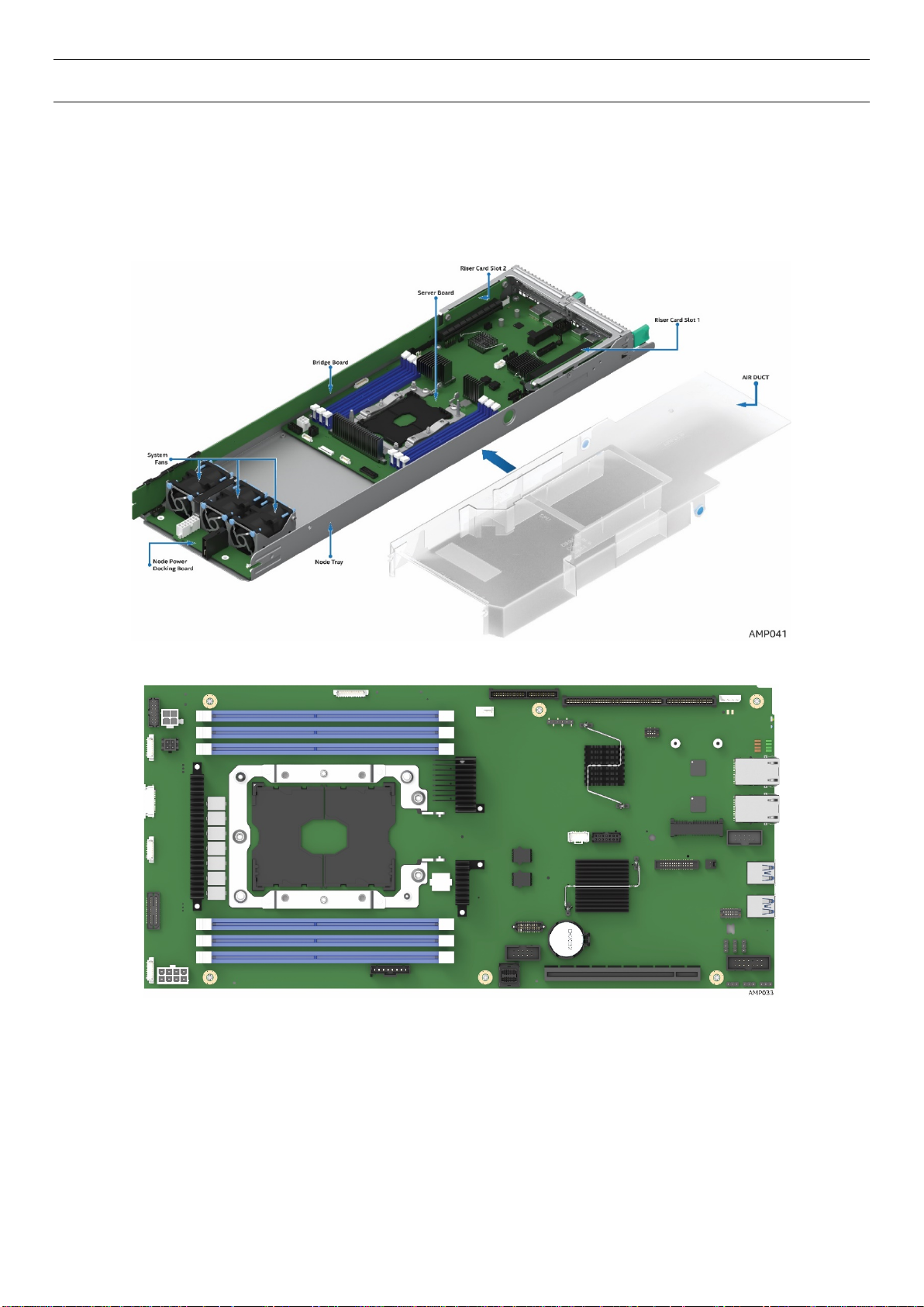
1 Product Features
This chapter briefly describes the main features of the Intel® Server Board S7200AP/APR and the Intel®
Compute Module HNS7200AP/APR. This includes illustrations of the products, a list of features, and
diagrams showing the location of important components and connections. The two main boards are
described in this document to include support for several chassis. The document includes updates for Intel®
Server Board S7200APR refresh product that is supported in the Intel® Server Chassis H2204XXLRE.
Figure 1. Intel® Compute Module HNS7200AP Product Family
Figure 2. Intel® Server Board S7200AP Product Family
Page 18

Feature
Description
Processor Support
Intel® Xeon™ Phi™ x200 Product Family
36 lanes of Integrated PCI Express® 3.0 low-latency I/O
Memory Support
Six DIMM slots in total across six memory channels
Max memory 384GB
Chipset
Intel C610 “Wellsburg” Platform Controller Hub (PCH)
External I/O Connections
Two USB 3.0 connectors
Two RJ-45 10/100/1000 Mbit Network Interface Controller (NIC) ports
Internal I/O
One USB 2.0 Header
One Serial Port A Header
PCIe Support
PCIe* 3.0 (2.5, 5, 8 GT/s)
Power Connections
• One 2x4 pin main power connector
One 4 pin power connector for disk drive power
System Fan Support
Three 40x56mm double rotor fans
One 4 pin CPU fan or liquid cooling pump support header
Video
128MB DDR3 memory
1.1 Product Feature Overview
1.1.1 Server Board Feature Set
Intel® Server Board S7200AP Product Family contains two server board options. Intel® Server Board
S7200AP supports Intel® Xeon™ Phi™ x200 CPUs (up to 230w TDP) in Intel® Server Chassis H2312XXLR2
and H2216XXLR2.
Intel® Server Board S7200APR supports both Intel® Xeon™ Phi™ x200 and Intel® Xeon™ Phi™ 72x5 Product
Family CPUs (up to 320w TDP) in Intel® Server Chassis H2204XXLRE.
This document describes the servicing of both compute modules. Although, these boards are
independent and stand-alone products, there are many features and service steps that are common to
each board. These common steps will be identified in its respective section.
The following tables list the common feature set, however, a board will be identified by its product code
when a described feature or function is unique to it.
Table 1. Intel® Server Board S7200AP Product Family Feature Set
connectors/headers
Single processor socket P (3647 pins)
Thermal Design Power (TDP) up to 230W
Registered DDR4 (RDIMM), Load Reduced DDR4 (LRDIMM)
Memory DDR4 data transfer rates of 2400/2666 MT/s
1 DIMM per channel
One TPM Header
One Intel® Omni-Path Fabric Signal Connector
One mSATA Connector
One Bridge Board Connector
One 2x7 pin header for system fan module
One Aux Front Panel Connector
Three 8-pin fan headers for non-Intel chassis support
One 4 pin CPU fan or liquid cooling pump support header
One PSU Control Header
One RMII header for Intel® RMM4 Lite
One internal RGB Video Header
• One 2x2 pin aux. power connector
•
Integrated 2D video graphics controller
Page 19

Feature
Description
Riser Support
One PCIe Gen3 x16 standard riser connector
On-board storage
controllers and options
Integrated 10-port SATA
o 4 ports to MiniSAS HD connector
Fabric
Dual port Intel® Omni-Path Fabric via
Single Port Intel® Omni-Path Fabric via x16 Gen 3 PCIe Adapter
Network (LAN)
Dual i210 Springvilles
to management traffic.
Server Management
Feature1
Description
Server Board
Intel® Xeon™ Phi™ x200 Product Family
CPUs with Integrated Intel® Omni-Path Fabric supported
Processor TDP Support
Maximum supported Thermal Design Power (TDP) of up to 230W
Heatsink
One 80x107mm 1U Heatsink
Fan
Three 40x56mm dual rotor system fans
Riser Support
One PCIe Gen3 x16 standard riser connector
Compute Module Board
One compute module power docking board
Air Duct
One transparent air duct
o Supports a low-profile adapter in Riser Slot 1
One PCIe Gen3 x20 HSEC-8 fine-pitch riser connector
o Supports a x16 low-profile adapter in Riser Slot 2
o Supports a x4 low-profile adapter in Riser Slot 2 when CPUs with
integrated Intel® Omni-Path Fabric are used
o 5 ports to bridge board,
o 1 port to mSATA
or
Dual 10/100/1000Gbe RJ45 connectors
NC_SI sideband to BMC. Option to host share or dedicate a Network port
Onboard Emulex* Pilot III* Controller
®
Support for Intel
Support for Intel
Support for Intel® Intelligent Power Node Manager
Remote Management Module 4 Lite solutions
®
System Management Software
Xeon™ Phi™ x200 Product Family
NOTE: The Riser Slot 1 on the server board is designed for plugging in ONLY the riser adapter. Plugging
in a PCIe* adapter directly into the riser slot may cause permanent server board and/or PCIe* card
damage.
1.1.2 HNS7200AP Compute Module Feature Set
Table 2. Intel® Compute Module HNS7200AP Product Family Feature Set
Single processor socket P (3647 pins)
Thermal Design Power (TDP) up to 230W
36 lanes of Integrated PCI Express® 3.0 low-latency I/O
One PCIe Gen3 x20 HSEC-8 fine-pitch riser connector
Bridge boards:
o Supports a low-profile adapter in Riser Slot 1
o Supports a x16 low-profile adapter in Riser Slot 2
o Supports a x4 low-profile adapter in Riser Slot 2 when CPUs
with integrated Intel® Omni-Path Fabric are used
o 6G SATA Bridge Board (Default)
Page 20

Feature1
Description
Form Factor
Length 14.17” (360m), width 6.81” (173mm)
Feature
Description
Dimensions (2U)
438mm x 86.9mm x 771/733mm
Node Support
Intel® Compute Module options:
Power Supply
2 x 2130W AC CRPS
System Cooling
3 dual rotor 40 x 56 mm fixed fans per node
PCIe support
Two low profile PCIe cards on riser 1 and 2
Storage
8 x 2.5” SATA drive Note: 2.5” SATA HDD installed in the 3.5” Drive Carrier
System SKUs
Support for H2312XXLR2 and H2216XXLR2 chassis only
NOTE: The table only lists features that are unique to the compute module or different with the server
board.
1. ONLY standard low profile PCIe* cards can be installed in the riser card slots.
1.1.3 Chassis Feature Set for Intel® Compute Module HNS7200AP
The following table lists a brief description of the 2U H2000G Chassis Product Family features,
17.24” width x 3.42 length x 30.35/28.86” height
HNS7200AP (up to four)
16 x 2.5” SATA drives
Bridge Board Options:
(1) 6G SATA only RAID 0, 1, 10 SW RAID ESRT2
Note: Intel® Compute Module HNS7200AP is not supported in Intel® Server Chassis H2204XXLRE
For additional details on chassis features, refer to the Intel® Server Chassis H2000G and H2000P Product
Family TPS and Service Guide.
Table 3. Intel® Server Board S7200APR (Refresh) Product Family Feature Set
Page 21

Feature
Description
Processor Support
Intel® Xeon™ Phi™ 72x5 Product Family
CPUs with Integrated Intel® Omni-Path Fabric supported
Memory Support
Six DIMM slots in total across six memory channels
Max memory 384GB
Chipset
Intel C610 “Wellsburg” Platform Controller Hub (PCH)
External I/O Connections
Two USB 3.0 connectors
Two RJ-45 10/100/1000 Mbit Network Interface Controller (NIC) ports
Internal I/O
One USB 2.0 Header
One Serial Port A Header
PCIe Support
PCIe* 3.0 (2.5, 5, 8 GT/s)
Power Connections
• One 2x4 pin main power connector
One 4 pin power connector for disk drive power
System Fan Support
Three 40x56mm double rotor fans
One 4 pin CPU fan or liquid cooling pump support header
Video
128MB DDR3 memory
Riser Support
One PCIe Gen3 x16 standard riser connector
On-board storage
o 4 ports to MiniSAS HD connector
Fabric
connectors/headers
Single processor socket P
Thermal Design Power (TDP) up to 320W with the 1U LACC thermal
solution
36 lanes of Integrated PCI Express® 3.0 low-latency I/O
Intel® Xeon™ Phi™ x200 Product Family
Single processor socket P (3647 pins)
Thermal Design Power (TDP) up to 230W (Air Cooled Heatsink)
36 lanes of Integrated PCI Express® 3.0 low-latency I/O
Registered DDR4 (RDIMM), Load Reduced DDR4 (LRDIMM)
Memory DDR4 data transfer rates of 2400/2666 MT/s
1 DIMM per channel
One TPM Header
One Intel® Omni-Path Fabric Signal Connector
One mSATA Connector
One Bridge Board Connector
One 2x7 pin header for system fan module
One Aux Front Panel Connector
Three 8 pin fan headers for third-party chassis support
One 4 pin CPU fan or liquid cooling pump support header
One PSU Control Header
One RMII header for Intel® RMM4 Lite
One internal RGB Video Header
• One 2x2 pin aux. power connector
•
Integrated 2D video graphics controller
o Supports a low-profile adapter in Riser Slot 1
One PCIe Gen3 x20 HSEC-8 fine-pitch riser connector
o Supports a x16 low-profile adapter in Riser Slot 2
controllers and options
Integrated 10-port SATA
Single Port Intel® Omni-Path Fabric via x16 Gen 3 PCIe Adapter
o Supports a x4 low-profile adapter in Riser Slot 2 when CPUs with
integrated Intel® Omni-Path Fabric are used
o 5 ports to bridge board,
o 1 port to mSATA
Page 22
Feature
Description
Network (LAN)
Dual i210 Springvilles
to management traffic.
RAID Support
Server Management
Onboard Emulex* Pilot III* Controller
Support for Intel
Intelligent Power Node Manager
Feature1
Description
Server Board
Intel® Xeon™ Phi™ 72x5 Product Family
CPUs with Integrated Intel® Omni-Path Fabric supported
Processor TDP Support
Maximum supported Thermal Design Power (TDP) of up to 320W
Heatsink
Liquid Assisted Air Cooling (LAAC)
Fan
Three 40x56mm dual rotor system fans
Riser Support
One PCIe Gen3 x16 standard riser connector
Compute Module Board
One compute module power docking board
Air Duct
One transparent air duct
Form Factor
Length 14.17” (360m), width 6.81” (173mm)
Dual 10/100/1000Gbe RJ45 connectors
NC_SI sideband to BMC. Option to host share or dedicate a Network port
Intel
Support for Intel
Support for Intel
®
Embedded Server RAID Technology 2 (ESRT2)
®
Remote Management Module 4 Lite solutions
®
System Management Software
®
NOTE: The Riser Slot 1 on the server board is designed for plugging in ONLY the riser adapter. Plugging
in a PCIe* adapter directly into the riser slot may cause permanent server board and/or PCIe* card
damage.
1.1.4 HNS7200APR Compute Module Feature Set
Table 4. Intel® Compute Module HNS7200APR Product Family Feature Set
Single processor socket P
Thermal Design Power (TDP) up to 320W with the 1U LACC
thermal solution
36 lanes of Integrated PCI Express® 3.0 low-latency I/O
Intel® Xeon™ Phi™ x200 Product Family
Single processor socket P (3647 pins)
Thermal Design Power (TDP) up to 230W (Air Cooled Heatsink)
36 lanes of Integrated PCI Express® 3.0 low-latency I/O
NOTE: The table only lists features that are unique to the compute module or different with the server
board.
1. ONLY standard low profile PCIe* cards can be installed in the riser card slots.
One 80x107mm 1U Heatsink-CPUs < 245W TDP
1U Liquid Assisted Air Cooling (LAAC) -CPUs > 245W TDP
o Supports a low-profile adapter in Riser Slot 1
One PCIe Gen3 x20 HSEC-8 fine-pitch riser connector
o Supports a x16 low-profile adapter in Riser Slot 2
o Supports a x4 low-profile adapter in Riser Slot 2 when CPUs
with integrated Intel® Omni-Path Fabric are used
Bridge boards:
o 6G SATA Bridge Board (Default)
Page 23
Feature
Description
Dimensions (2U)
438mm x 86.9mm x 771/733mm
Node Support
Intel® Compute Module options:
Power Supply
2 x 2130W AC CRPS
System Cooling
3 dual rotor 40 x 56 mm fixed fans per node
PCIe support
Two low profile PCIe cards on riser 1 and 2
Storage
4 x 2.5” SATA drive Note: 2.5” SATA HDD installed in the 3.5” Drive Carrier
System SKUs
Supported for H2204XXLRE chassis only
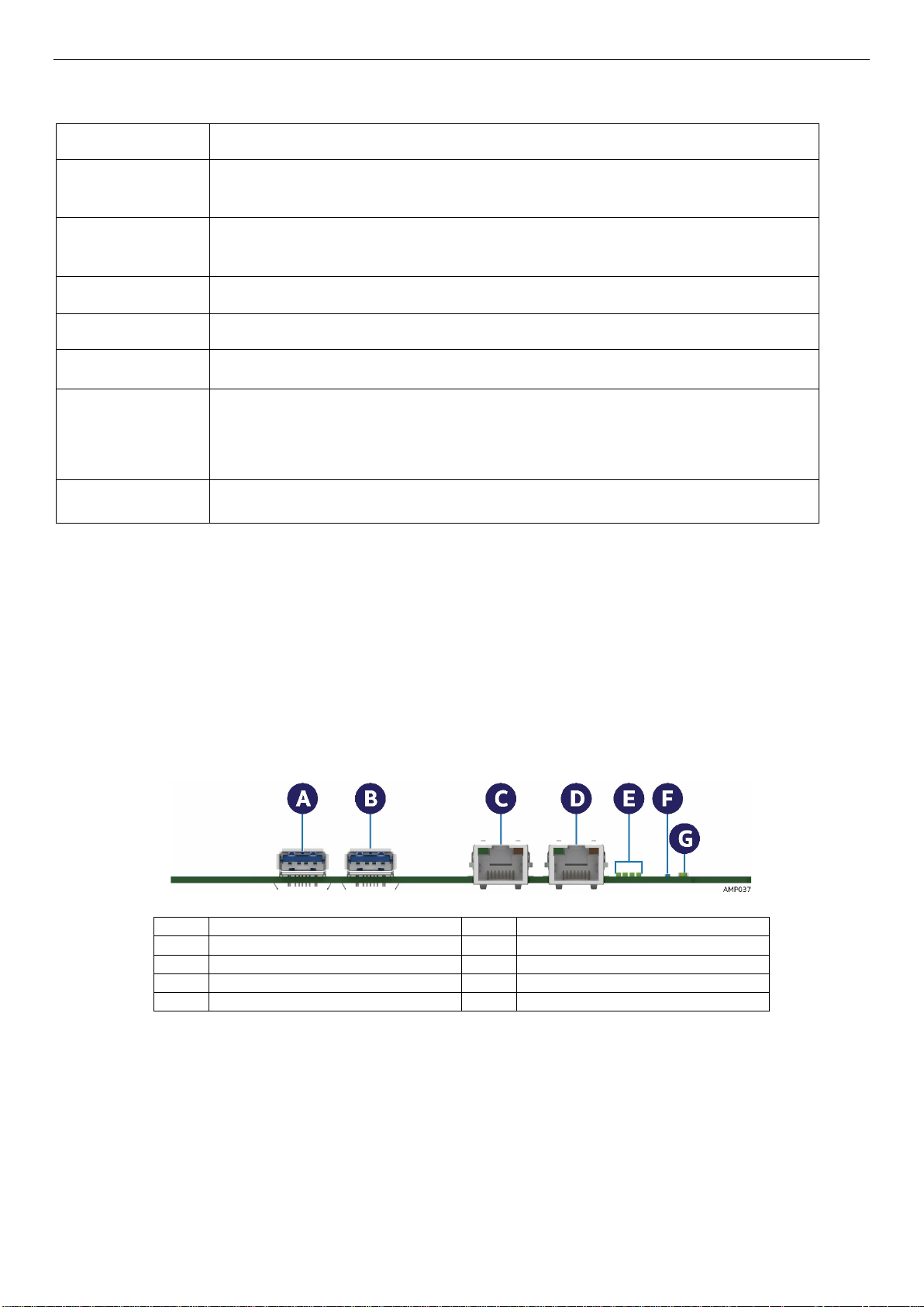
Label
Description
Label
Description
A
USB 3.0 Por t 1
B
USB 3.0 Por t 2
C
NIC port 1 (RJ45)
D
NIC port 2 (RJ45)
E
POST Code LEDs (8 LEDs)
F
ID LED
G
Status LED
1.1.5 Chassis Feature Set for Intel® Compute Module HNS7200APR
The following table lists a brief description of the 2U H2000-G Chassis Product Family features
17.24” width x 3.42 length x 30.35/28.86” height
HNS7200APR (up to four)
Bridge Board Options:
(1) 6G SATA only RAID 0, 1, 10 SW RAID ESRT2
Note: Intel® Compute Module HNS7200APR is not supported in Intel® Server Chassis H2312XXLR2 and
H2216XXLR2
For additional details on chassis features, refer to the Intel® Server Chassis H2000G Product Family TPS.
1.2 Back Panel Feature Identification
The Intel® Compute Module HNS7200AP product family has the following board rear connector placement
and features.
Figure 3. Intel® Server Board S7200AP Rear Connectors
Page 24
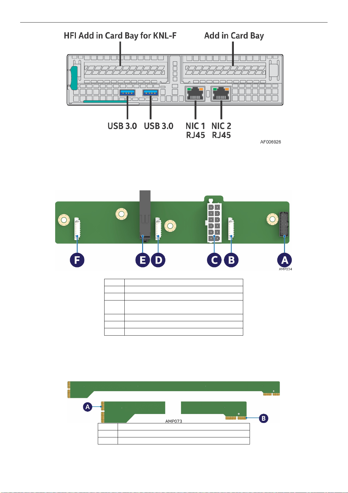
Label
Description
A
2x7 pin fan control connector
B
8 pin connector for fan 1
C
2x6 pin Minifit Jr. main power output
connector
D
8 pin connector for fan 2
E
12 pin connector for main power input
F
8 pin connector for fan 3
Label
Description
A
2x40 pin card edge connector (to the backplane)
B
2x40 pin card edge connector (to the baseboard slot)
Figure 4. Intel® Compute Module HNS7200AP Rear Connectors
1.3 Power Docking Board Features
Figure 5. Power Docking Board Features
1.4 Bridge Board Feature Features
Figure 6. 6G SATA Bridge Board Features
Page 25
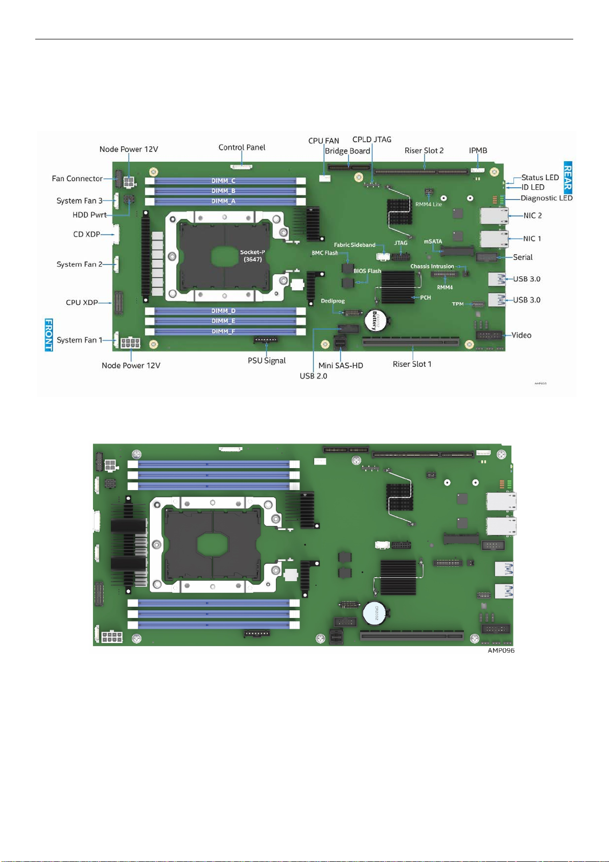
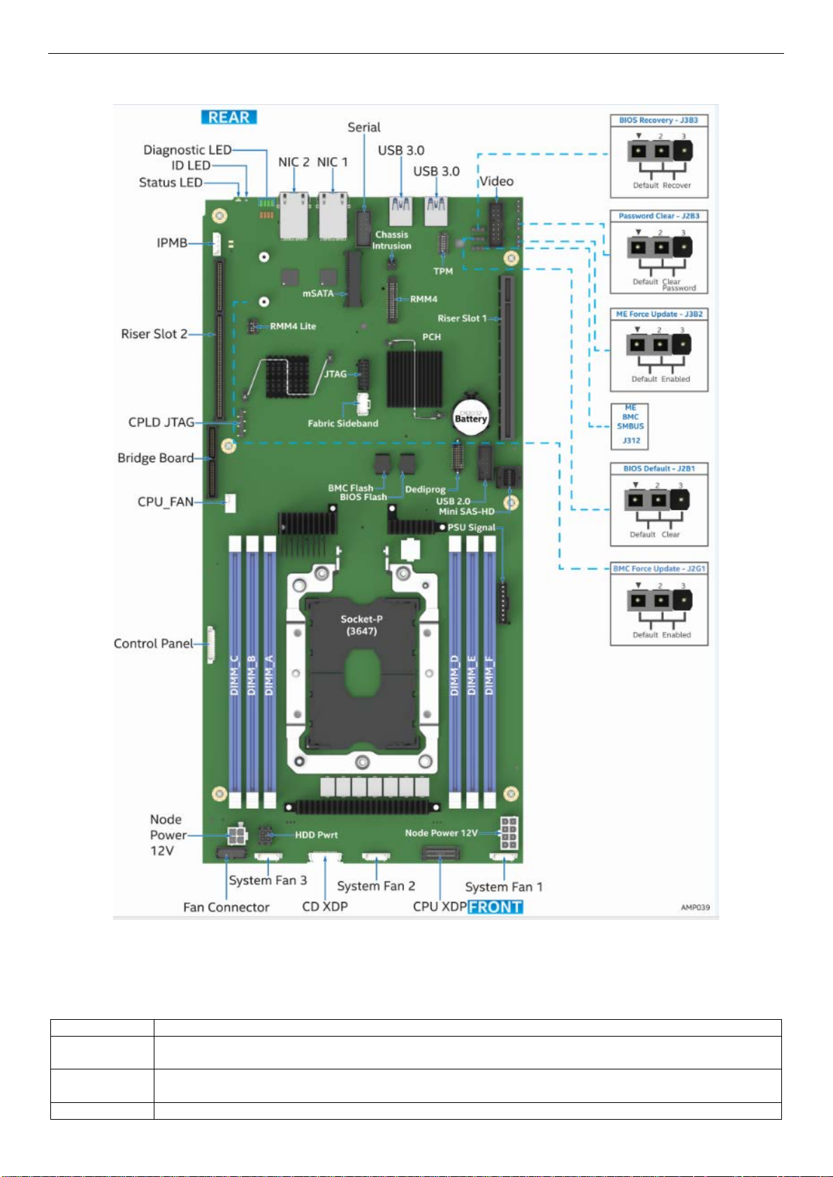
1.5 Server Board Features
This section helps you identify the components and connectors on the server board. Intel® Server Board
S7200AP features shown. All major features that are called out are common to both boards.
Figure 7. Intel® Server Board S7200AP Features
Figure 8. Intel® Server Board S7200APR
Page 26
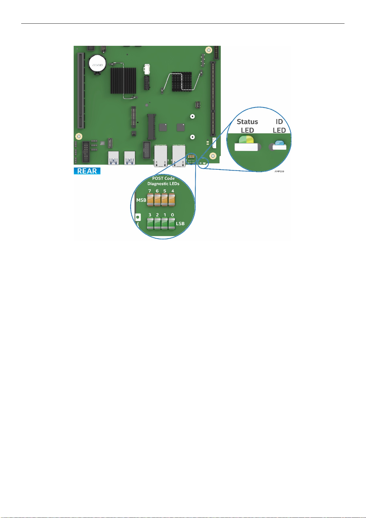
1.6 Intel® Light-Guided Diagnostics
Figure 9. Intel® Light-Guided Diagnostic LEDs – Server Board
The POST Code Diagnostic LEDs on the server board change color or state (off, green, red, and amber)
according to the POST sequence.
The Status LED on the rear of the board shows the overall health of the system (green, blinking green,
blinking amber, amber, and off).
The Identification LED on the rear of the board helps identify the server from among several servers. The
ID LED is off by default, and blue when activated by button or software.
Page 27
Jumper Name
Description
BMC Force
Update (J2G1)
If pins 2-3 are selected, the Integrated BMC Force Update Mode is enabled. These pins should be selected
on 1-2 for normal system operation.
BIOS Default
(J2B1)
If pins 2-3 are selected, the BIOS settings are restored to the factory defaults on the next reset. These pins
should be selected on 1-2 for normal system operation.
BIOS Recovery
If the system BIOS is corrupted, an onboard backup copy of the BIOS can be loaded using the BIOS
1.7 Configuration and Recovery Jumpers
Figure 10. Configuration and Recovery Jumpers
Page 28

(J3B3)
Recovery Jumper. To load the backup BIOS image, move the jumper from pins 1-2 (default) to pins 2-3, and
for normal system operation.
Password
Clear(J2B3)
If pins 2-3 are selected, administrator and user passwords are cleared within five to ten seconds after the
system is powered on. These pins should be selected on 1-2 for normal system operation.
ME Force
Update (J3B2)
If pins 2-3 are selected, the ME Force Update Mode is enabled. These pins should be selected on 1-2 for
normal system operation.
power on the system. The system will boot to the backup BIOS image. These pins should be selected on 1-2
1.8 Advanced Management Options
1.8.1 Intel® Remote Management Module 4 Lite
The Intel® Remote Management Module 4 Lite plugs into a dedicated connector on the server board and
provides additional server management functionality to the compute module.
The Intel® Remote Management Module 4 Lite, together with the dedicated management port provides a
dedicated web server for viewing server information and remote control of the compute module. It also
provides Remote KVM Redirection and USB Media Redirection allowing USB devices attached to the remote
system to be used on the managed server.
For instructions on installing the Intel® Remote Management Module 4 Lite, see section 2.10.
Page 29
2 Hardware Installations and Upgrades
2.1 Before You Begin
Before working with your server product, closely review the Safety Information at the beginning of this
document.
NOTE: Prior to servicing the compute module or chassis, power down the server, unplug all peripheral
devices and the AC power cords.
2.1.1 Tools and Supplies Needed
• Phillips* (cross head) screwdriver (#1 bit and #2 bit)
• T30 Tor x bit screwdriver
• Flat head screwdriver
• Needle nosed pliers
• Anti-static wrist strap and conductive foam pad (recommended)
2.1.2 System Reference
All references to left, right, front, top, and bottom assume that the reader is facing the front of the chassis
as it would be positioned for normal operation.
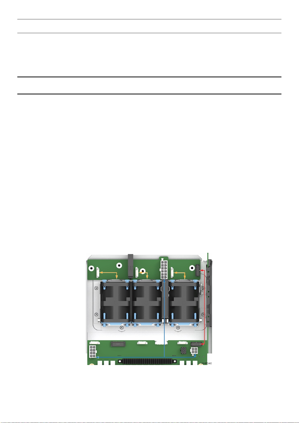
2.2 Cable Routing
Each compute module is self-contained and can be hot swapped without any impact to other compute
modules. When you add or remove components from the compute module enclosure, ensure that cables
are routed correctly before plugging in the compute module back into the chassis. Use caution to ensure
that cables or wires are not pinched and that the airflow from the fans is not blocked. Use the figures
below to determine the correct cable routing. Section 2.2 applies to both server boards.
Figure 11. Cable Routing
NOTES:
• Orange line: Fan cable connection
• Blue line: Server board power cable connection
• Red line: Fan control signal cable connection
Page 30
2.3 Removing and Installing the Air Duct
Always operate your compute module with the air duct in place. The air duct is required for proper airflow
within the compute module. Intel® Server Board S7200AP. Section 2.3 applies to both server compute
module.
2.3.1 Removing the Air Duct
1. Press and hold both the left and right side buttons of the air duct (See letter A).
2. Rotate the air duct more than 45 degrees and pull it out. (See letter B).
Figure 12. Removing the Air Duct
Page 31

2.3.2 Installing the Air Duct
NOTES: Ensure that all DIMM latches are closed before installing the air duct.
1. Align the front end of the air duct with the hinges on both sides of the fan bracket (See letter A).
2. Rotate the air duct (See letter B) and lower it down until the left and right side buttons snaps into place.
Figure 13. Installing the Air Duct
Page 32

2.4 Processor Assembly Installation and Removal
2.4.1 Assembling the Processor Heat Sink Module (PHM)
The processor heat sink module (PHM) refers to the sub-assembly where the heat sink and processor are
attached together prior to installation onto the server board.
Figure 14. Processor Heatsink Module (PHM) and Processor Socket Reference Diagram
Procedures described in the following sections must be followed in the order specified to properly
assemble the PHM, install it to, or remove it from the server board. These instructions assume that all the
PHM components are new and the thermal interface material (TIM) is already applied to the bottom of the
heat sink.
Required Tools:
• T-30 Torx screwdriver
• Flat head screwdriver
• Adequate ESD protective gear (wrist strap, ESD mat)
CAUTION: Refer to the “Warning” section at the beginning of this document for detailed ESD
precautions.
NOTE: Fabric supported processor models require the use of a Fabric Carrier assembly. Fabric Carrier
assemblies are sold separately and can be obtained by ordering the following Intel Accessory Kit - iPC
Page 33

Carrier Clip Model
iPN*
Carrier Clip Assembly
Standard Processor Carrier
AXX2PFABKIT. Refer to the Product Configuration Guide for this Intel Server product family for
additional ordering details.
WARNING: Attempting to use a standard processor carrier clip assembly with a fabric supported
processor may result in component damage and/or induce improper assembly of the PHM. See the
following table and figures for an overview of the different processor carrier and processors.
Table 5. Processor Carriers
(Default) Included with
Systems
H53249-00x
Fabric Processor Carrier
(Accessory)
H53248-00x
NOTE: * For reference only. Intel part numbers (iPN) are not used for ordering purposes.
Intel parts that are available as a Spare or Accessory are orderable via Intel Product Codes (iPC).
Figure 15. Processor Reference Diagram - Top and Bottom Views of Processor
Page 34

WARNING: Damage to the processor heat sink may occur when grasping the heat sink by the longer sides
and squeezing fins together. Processor heat sinks should only be grasped using the shorter edges of the
heat sink as shown in the following illustration.
Figure 16. Grasping the Heatsink Correctly
1. Remove the heat sink from its packaging. With the thermal interface material (TIM) facing up, place the
heat sink on to a flat surface as shown in the following illustration.
Figure 17. Placing the Processor Heat Sink on to a Flat Surface
CAUTION: Do not touch the sensitive contacts on the bottom side of the processor at any time
during PHM assembly or installation. In addition, the pins inside the processor socket are
extremely sensitive. A damaged processor socket may produce unpredictable system errors
2. If present, carefully remove the plastic protective cover from the bottom side of the processor.
NOTE: The PHM and processor socket include several alignment features as shown in the
following illustration to ensure proper assembly and installation. Care should be taken to ensure
components are accurately assembled and the PHM is oriented correctly to the processor socket
prior to installation.
Page 35

CAUTION: Handle the processor carefully. Do not touch the bottom-side contacts or components,
always grip the processor by its edges.
Figure 18. Alignment Features
Page 36

3. Orient the processor with the heat spreader side down so its alignment features match those of the
carrier clip as shown in the following figures.
Figure 19. Processor Carrier Assembly
4. Install the processor into the processor carrier clip until it snaps into place.
Figure 20. Processor Carrier Clip Sub-Assembly
CAUTION: A processor can dislodge from the processor carrier clip if the assembly is grasped by
the long narrow edges of the processor clip. The processor carrier assembly should only be
grasped using the shorter edges of the assembly.
5. If present, remove the protective film covering the TIM on the bottom side of the heat sink.
Page 37

6. Orient the processor carrier clip sub-assembly over the processor heat sink so that all corner features
are in alignment.
Figure 21. Orienting Processor Carrier Clip Sub-assembly to Heat Sink
7. Push the processor carrier clip sub-assembly down on to the processor heat sink until it snaps into
place, ensuring all four corners are secure.
Figure 22. Processor Heat Sink Module (PHM)
Page 38

2.4.2 Processor Installation
iPC - AXXAPHS
Table 6. Processor Heat Sinks
Intel Product Code (iPC) MM# Description
MM# - 942344
1U Standard Ex-Al 80mm x 107mm Heat
Sink
Figure 23. Processor Heat Sink Location
Page 39

1. Remove the plastic processor socket cover. Grasp the socket cover using the finger grips on each end
as shown in the following figure, (See letter A) then carefully pull up to remove (See letter B).
Figure 24. Plastic processor socket cover removal
NOTE: The processor socket cover should be saved for future use.
CAUTION: When re-installing the socket cover, make sure it properly snaps into place. Improper
installation will cause it to become loose and damage the processor socket.
2. Install PHM to Processor socket.
a. Align the mounting holes of the PHM (located on diagonal corners) to the bolster plate guide pins
of the processor socket as shown in the following figure.
Page 40

NOTE: Each of the two guide pins of the bolster plate has a different diameter. Each guide pin will have a
matching PHM mounting hole which allows for only one orientation when installed as shown in the
following figure. Look for the wide and narrow holes for proper and accurate alignment.
Figure 25. PHM Alignment to Bolster Plate
b. Lower the PHM onto the processor socket assembly.
CAUTION: Processor socket pins are delicate and bend easily. Use extreme care when placing the PHM
onto the processor socket.
Page 41

NOTE: See the illustration below and confirm proper PHM installation by visually checking whether or not
the PHM sits level with the processor socket assembly. The PHM is NOT installed properly if it does not sit
level with the processor socket assembly. Improperly installed PHMs cannot be fastened down. PHMs
can only be fastened down if correctly installed.
Figure 26. Correct Placement
3. Secure PHM to the processor socket assembly.
a) Using a T30 Torx bit screwdriver, securely tighten (12 in-lb.) each nut in the sequence shown on
the label located on the top of the heat sink. Follow the (#1→ #2 → #3→ #4) sequence when
tightening. Tighten each screw prior to moving to the next.
Figure 27. Installing the PHM
CAUTION: Failure to tighten the heat sink screws in the specified order may cause damage to the
processor socket assembly. Each heat sink screw should be fully tightened to 12 in-lb torque before
securing the next screw in the sequence.
Page 42

2.5 Processor Removal
WARNING: Processor heat sinks can become extremely hot during normal system operation. Before
attempting to remove the processor from the server board, ensure system power has been fully
disconnected and allow the processor heat sinks to fully cool before attempting to remove the PHM from
the server board.
1. Using a T30 Torx bit screwdriver, loosen each heat sink nut in the sequence shown on the label
affixed to the top side of the heat sink (#4→ #3 → #2→ #1) (See letter A). Loosen each screw all the
way prior to moving to the next.
2. Lift the PHM straight up from the server board until free from the bolster plate guide pins (See letter
B).
3.
Figure 28. Uninstalling the PHM
4. If a processor is not being installed, re-install the plastic processor socket cover.
Figure 29. Plastic processor socket cover Installation
Page 43

2.5.1 PHM Disassembly
1. Place the PHM (heat sink down) onto a flat surface.
2. To remove the processor and clip sub-assembly from the heat sink, using a flat head screw driver,
carefully release the bond between processor and heat sink as shown in the following illustration.
Figure 30. PHM Disassembly
3. Unlatch the hooks on each corner of the processor carrier clip to free the processor carrier from the
heat sink.
4. Carefully lift the processor sub-assembly away from the heat sink.
Figure 31. Releasing the Processor Carrier Clip from the Heat Sink
Page 44

5. Remove the processor from the processor carrier by carefully pushing back one of the latches located
on the ends of the processor and rotating the processor up and out of the processor carrier.
Figure 32. Releasing Processor from Carrier
Page 45
2.6 Installation and Removal of the 1U LACC
Intel® Server Board S7200APR and Intel® Server Compute Module HNS7200APRL product family support
the Intel® Xeon™ Phi™ processors Bootable CPUs (up to 320W TDP) in Intel® Server Chassis H2204XXLRE.
All Intel® Xeon™ Phi™ Processors x200 or 72x5 CPU SKUs at 245W or greater TDP require use of the Intel®
1U Liquid Assisted Air Cooling (LACC) solution for optimal thermal support. The Intel® Server Board
S7200APR product family Technical Product Specfication (TPS) decribes the 1U LAAC in detail. This
section of the Service Guide describes the installation and removal of the 1U LACC coolling solution.
Note: Passive Air Cooled Heatsinks are not supported on CPUs with TDPs equal to or higher than 245w
regardless of the supported CPU generation.
2.6.1 Removal of the 1U LACC Assembly
Figure 33. 1U LACC Assembly
Figure 34. 1U LACC Assembly installed in the system
Page 46

1. Power off the compute module and disconnect the power cable(s).
2. Remove the air duct. See section 2.3.1
3. Disconnect the pump cable that is connected to the 4-pin CPU Fan Header (J6J2)
.
Figure 35. Disconnect the Pump Cable (Fan Header J6J2)
4. Next, remove the LACC Heat Exchanger retaining brackets by removing the 4 screws.
Figure 36. Remove LACC brackets #1
Page 47

Figure 37. Remove LACC brackets #2
Figure 38. Remove LACC brackets #3
5. Finally, remove the LACC Cold Plate assembly. The LACC cold plate assembly is modeled after the
passive air heatsink assembly. The sequence and method of removing the cold plate is exactly the
same as the passive air heatsink. Follow carefully the screw loosening sequence. Refer to the passive
air heatsink removal instructions in Section 2.5
for detail.
Page 48

Figure 39. Remove Cold Plate Assembly
6. Carefully lift the LACC Assembly away from the node. Use two hands to grasp the heat exchanger and
cold plate to safely remove the LACC assembly.
Figure 40. Lift out LACC Assembly
Page 49

2.6.2 Remove the CPU and Carrier Assembly
1. Power off the compute module and disconnect the power cable(s).
2. Remove the air duct. See section 2.3.1
3. Follow the procedures in Section 2.6.1 for LACC assembly removal
4. Turn the LACC and cold plate assembly over as shown in Figure 41
5. The LACC cold plate assembly is modeled after the passive air heatsink assembly. The sequence and
method of removing the CPU and Carrier is exactly the same as the passive air heatsink. This step is
only required if the CPU requires replacement. For simplification, refer to the CPU and Carrier
removal instructions in Section 2.5
.
for detail.
Figure 41. Releasing CPU and Carrier from Cold Plate
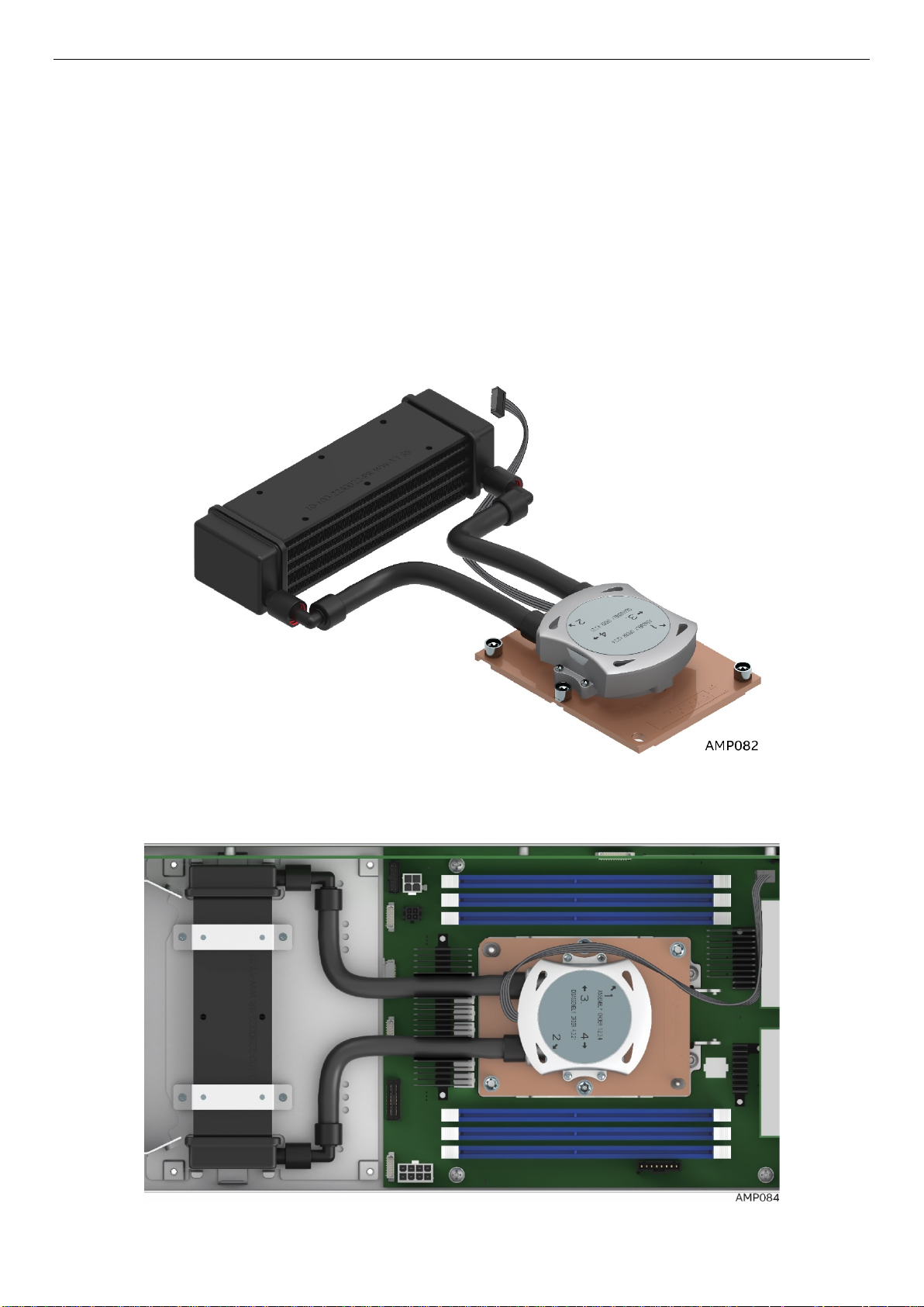
2.6.3 Install the 1U LACC Assembly
Figure 42. 1U LACC Assembly
Page 50

1. Power off the compute module and disconnect the power cable(s).
2. Remove the air duct. See section 2.3.1
3. The LACC cold plate assembly is modeled after the passive air heatsink assembly. The sequence and
method of installing the CPU and Carrier is exactly the same as the passive air heatsink. This step is
only required if the CPU requires replacement or installation. For simplification, refer to the CPU and
Carrier installation instructions in Section 2.4
.
for detail.
Figure 43. Install CPU and Carrier to Cold LACC Cold Plate
4. Carefully place and position the LACC assembly back into the system by using two hands. Ensure that
it is properly aligned and that the cold plate aligns correctly with the CPU socket assembly and guide
pins.
Page 51

Figure 44. Install the LACC assembly into the system
5. Next, align and install the LACC cold plate assembly. Tighten the LACC Cold Plate assembly nuts. The
LACC cold plate assembly is modeled after the passive air heatsink assembly. The sequence and
method of tightening the cold plate screws is exactly the same as the passive air heatsink. Follow the
tightening sequence carefully. Refer to the passive air cooled heatsink installation instructions in
Section 2.4
for detail.
Figure 45. Install the LACC assembly into the system
6. Install the LACC Heat Exchanger retaining brackets by installing the 4 screws.
Figure 46. Install brackets #1
Page 52

Figure 47. Install LACC brackets #2
Figure 48. Install LACC brackets #3
Page 53

7. Connect the pump cable to the 4-pin CPU Fan Header (J6J2)
Figure 49. Connect the Pump Cable (fan header J6J2)
Page 54

2.7 Removing and Installing Riser 1 and Riser 2
2.7.1 Remove Riser 1
1. Power off the compute module and disconnect the power cable(s).
2. Remove the air duct. See section 2.3.1
3. Loosen the 3 screws (See A )
4. Pull the riser straight up and out of the system (See B and C)
.
Figure 50. Removing Riser 1
2.7.2 Install Riser 1
1. Power off the compute module and disconnect the power cable(s).
2. Remove the air duct. See section 2.3.1
3. Align and insert Riser 1 into Riser Slot 1 (See A)
4. Ensure that the Riser is all the way down and fully seated (See B)
5. Tighten the 3 screws (See C)
.
Page 55

Figure 51. Installing Riser 1
2.7.3 Remove Riser 2
1. Power off the compute module and disconnect the power cable(s).
2. Remove the air duct. See section 2.3.1
3. Loosen the 3 screws (See A )
4. Pull and lift the riser straight up and out of the system (See B and C)
.
Figure 52. Removing Riser 2
2.7.4 Install Riser 2
1. Power off the compute module and disconnect the power cable(s).
2. Remove the air duct. See section 2.3.1
3. Align and insert Riser 2 into Riser Slot 2 (See A)
4. Ensure that the Riser is all the way down and fully seated (See B)
.
Page 56

5. Tighten the 3 screws (See C)
Figure 53. Installing Riser 2
2.8 Installing and Removing an Add-In Card - Riser Slot 1
2.8.1 Installing a PCIe* Add-In Card Riser 1
1. Power off the compute module and disconnect the power cable(s).
2. Remove the air duct. See section 2.3.1
3. Remove Riser 1 See section 2.7.1
4. Remove the filler panel and attach the Add-In Card to the riser card assembly.
5. Insert the PCIe* Add-In Card into the riser slot (See letter A).
.
Figure 54. Installing the PCIe* Add-In Card– Step 1
Page 57

6. Align and insert the PCIe* riser assembly into the Riser Slot 1 on the server board (See letter B).
Figure 55. Installing the PCIe* Add-In Card – Step 2
7. Install and tighten the three screws (See letter C).
Figure 56. Installing the PCIe* Add-In Card – Step 3
2.8.2 Removing a PCIe* Add-In Card Riser 1
1. Loosen the three screws (See letter A).
Page 58
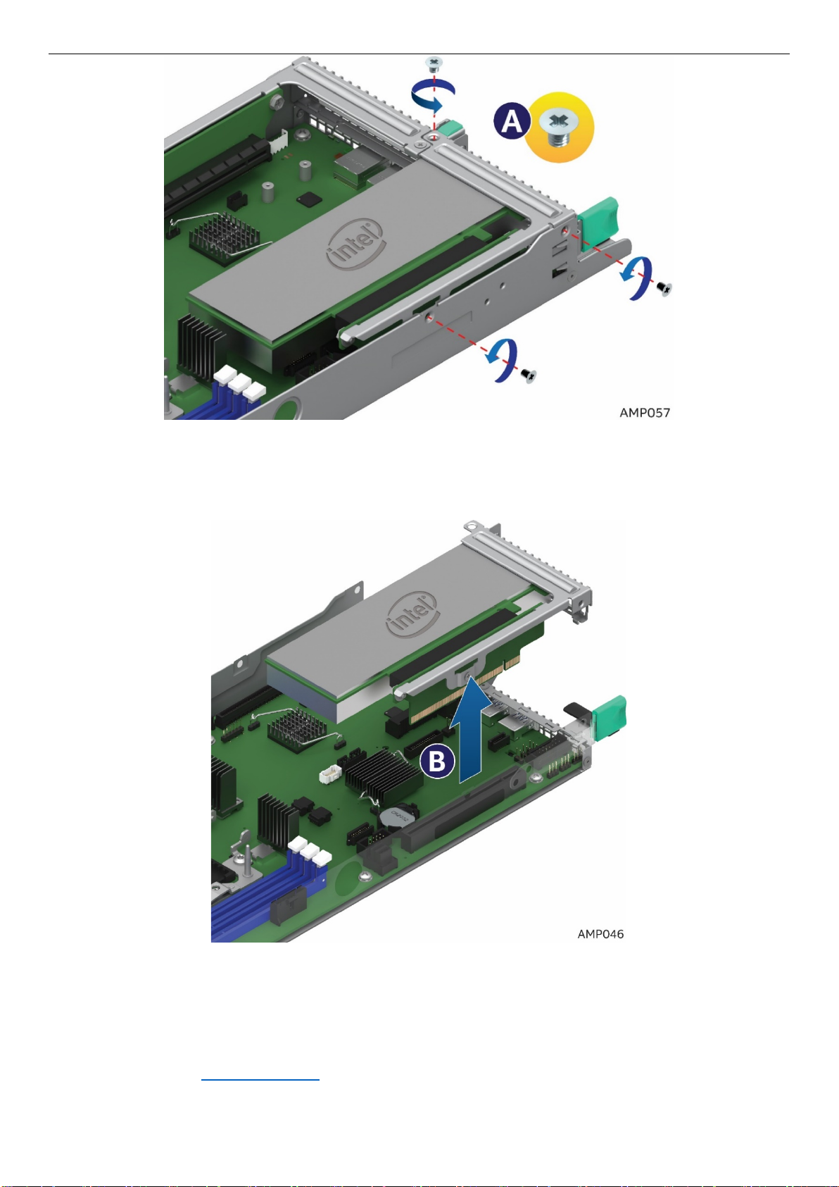
Figure 57. Removing the PCIe* Add-In Card – Step 1
2. Pull the Add-In Card assembly up and out (See letter B).
Figure 58. Removing the PCIe* Add-In Card – Step 2
3. Remove the Add-In Card from the riser (See letter C).
4. Re-install the filler panel
5. Re-install Riser 1 See section 2.7.2
Page 59

Figure 59. Removing the PCIe* Add-In Card– Step 3
2.9 Installing and Removing an Add-In Card - Riser Slot 2
2.9.1 Installing a PCIe* Add-In Card Riser 2
Note: Riser Slot 2 has two Riser options. Select the appropriate Riser (PCIe*X8 or X16 riser for slot 2) for
your configuration. See the product configuration guide and technical product specification for details.
1. Power off the compute module and disconnect the power cable(s).
2. Remove the air duct. See section 2.3.1
3. Remove Riser 2 See section 2.7.3
4. Remove the filler panel and attach the Add-In Card to the riser card assembly.
5. Insert the PCIe* Add-In Card into the riser slot (See letter A).
.
Page 60

Figure 60. Installing the PCIe* Add-In Card– Step 1
6. Align and insert the PCIe riser assembly into the Riser Slot 1 on the server board (See letter B).
Figure 61. Installing the PCIe* Add-In Card– Step 2
7. Ensure that the Add-In Card and Riser are fully seated (See letter C).
8. Tighten the three screws (See letter D).
Figure 62. Installing the PCIe* Add-In Card– Step 3
Page 61

2.9.2 Removing a PCIe* Add-In Card from Riser 2
1. Power off the compute module and disconnect the power cable(s).
2. Remove the air duct. See section 2.3.1
3. Loosen the three screws (See letter A).
4. Pull straight up on Riser 2 with the PCIe* Add-In Card assembly (See letter B).
.
Figure 63. Removing the PCIe* Add-In Card – Step 1
5. Lift out the PCIe* Slot 2 Riser with Add-In-Card.
Page 62
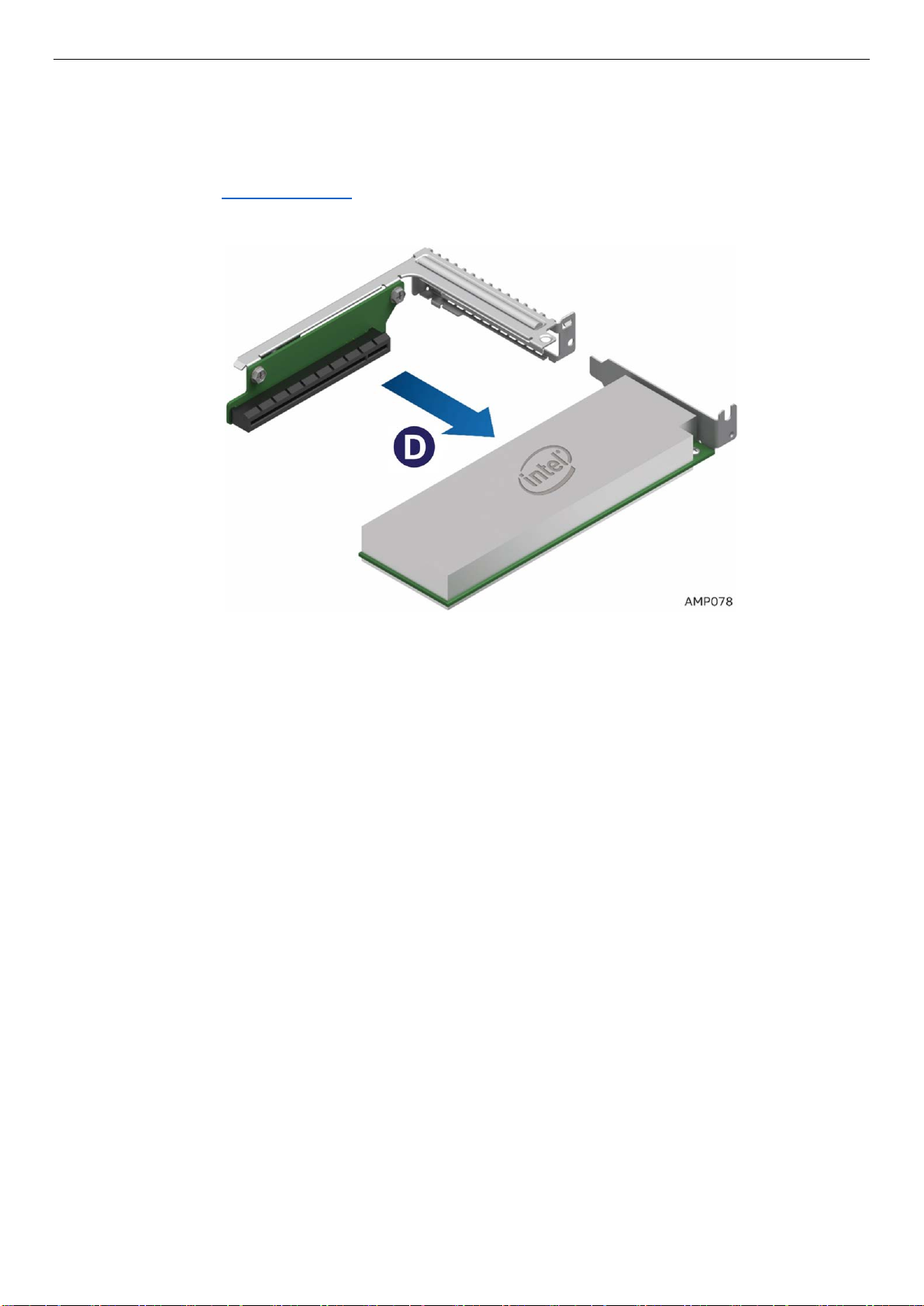
Figure 64. Lift out the Riser and Add-In-Card– Step 2
6. Remove the Add-In Card from the riser (See letter D).
7. Re-install the filler panel
8. Re-install Riser 2 See section 2.7.4
Figure 65. Remove the Add-In-Card from Riser 2– Step 3
2.10 Installation and Removal of the Intel® Omni-Path Fabric
Processor Kit.
The Intel® Xeon™ Phi™ x200 Product Family CPUs with integrated Intel® Omni-Path Fabric is required for
use in conjunction with the Intel® Fabric Through (IFT) carrier for full fabric connectivity. The following
sections will provide procedures on how to install and remove the optional Intel® Omni-Path Fabric
Processor Kit (iPC – AXX2PFABKIT) and the Intel® Xeon™ Phi™ (Fabric) processor. The IFT Carrier card is
installed in PCIe* Riser Slot 1. Refer to the S7200AP Family Configuration Guide & Spares/Accessories List
for ordering details.
Note: The Intel® Omni-Path Fabric Processor Kit is not supported when Intel® Xeon™ Phi™ 72x5 Product
Family CPUs are installed.
2.10.1 Fabric Processor Kit Components
1. The Intel® Omni-Path Fabric Processor Kit consists of the following components:
a) Intel® Fabric Through (IFT) carrier card
b) Intel® Omni-Path Fabric Sideband Cable
c) Intel® Omni-Path Fabric Processor Cable
d) Fabric CPU carrier assembly
Page 63

Figure 66. Installing the IFT Carrier
2.10.2 Fabric Processor Kit Cables
1. The two cables are included with the kit. Cables are labeled for illustration purposes.
Figure 67. Intel® Omni-Path Sideband Cable Connection
Figure 68. Intel® Omni-Path Fabric Processor Cable
Page 64

2.10.3 Installing the Fabric Processor Kit
1. Power off the compute module and disconnect the power cable(s).
2. Remove the air duct. See section 2.3.1
3. See section 2.4.1 for instructions on how to assemble the (processor heat sink module) PHM, fabric
CPU carrier assembly and mount it onto the server board. Note that the fabric carrier clip that comes
with the kit must be used with the fabric CPU.
4. Remove the Fabric Processor Kit components
5. For ease of installation, prior to installing the carrier card into Riser 1, install the sideband cable (P2,
black end) into carrier card connector J3A1 on the carrier card (See letter A in figure 51). Leave the
other end of the cable (P1, white end) disconnected for later installation into the main board
sideband fabric connector J5J2.
6. PCSD customers should ensure that IFT Carrier Card Jumper J1A2 is set for pin position 2-3 for
normal operation.
NOTE: The actual view of the IFT carrier card has been modified in order to illustrate the sideband
cable connection (See Figure 51). The card will be rotated 180° and thee IFT carrier ports face down
in Riser Slot 1 when installed in the system.
.
Figure 69. Sideband Cable Connection
7. Install the IFT carrier card.
Note: The IFT card should be installed in PCIe* Slot 1 for normal operation with the Intel® Xeon™ Phi™
(Fabric) processor. The IFT carrier card is not supported in PCIe* Slot 2 when the fabric CPU is
installed. When the Intel® Xeon™ Phi™ (Fabric) processor is used in the server system, PCIe* Slot 2 is
reduced to x4 lanes (electrical) for PCIe* device connectivity. See the Intel
®
Server Board S7200AP
and Intel® Compute Module HNS7200AP Product Family Configuration Guide and Technical Product
Specification for Riser 2 options.
a) Follow the basic instructions to install an Add-In-Card in Slot 1 as shown in section 2.7.1. Install the
IFT card into Riser Slot 1 card (See Figure 52, letter A). Note that the sideband cable (P2, black end)
is already connected to the IFT carrier card prior to installing the carrier card into Riser 1.
b) Install IFT and Riser Slot 1 card into Riser slot 1 (See Figure 52, letter B).
c) Secure the riser card (See Figure 52, letter C).
d) Once the IFT Carrier Card is fully secured in the system, connect the other end of the sideband cable
(P1, white end) into the main board sideband fabric connector J5J2. Refer back to Figure 51 (See
Page 65

letter B), Sideband Cable Connection.
Figure 70. Installing the IFT Carrier
5. Install the Intel® Omni-Path Fabric Processor Cable
a) Line up the cable CPU connector end and install it vertically onto the Fabric CPU connector. Push
the connector forward toward the substrate until fully engaged. (See letter A)
b) Rotate and snap the cable wire latch into the lock position onto the bolster plate latch posts.
c) Insert the two IFP plugs into the IFT carrier slots on the board. When installing the two plugs, the
latch release buttons are marked P1 and P2 will face down in the system. As illustrated, ensure that
the connector marked P1 on the cable is inserted into the P1 connector and the P2 plug is inserted
into the P2 connector (See letter B). Ensure that the cables are pushed fully forward and are fully
engaged.
d) At the rear of the system, plug in the fabric cable. See the Intel® Omni-Path Cables Matrix for a list
of supported cables:
fabrics/omni-path-cables.html
http://www.intel.com/content/www/us/en/high-performance-computing-
Page 66

Figure 71. Fabric Processor and IFT Cable Connections
Page 67

2.10.4 Removing the Fabric Processor Kit
1. Disconnect all the cable connections from the IFT carrier and the fabric processor
(See letter A, B and C).
Figure 72. Disconnecting IFP Cables
2. See section 2.8.2
for instructions on how to remove the Intel® Omni-Path / Fabric processor carrier card
from Riser 1.
3. See section 2.5 for instructions on how to remove the processor from the server board.
Page 68

2.11 Installing and Removing the Memory
2.11.1 Installing the Memory
1. Power off the compute module and disconnect the power cable(s).
2. Remove the air duct. See section 2.3.1
3. Locate the DIMM socket. Make sure the clips at either end of the DIMM socket are pushed outward to
an open position (See letter A).
NOTE: Make sure the retaining clip of the adjacent slot is NOT open and does NOT interfere with
each other.
CAUTION: Add-In Cards may need to be removed prior to servicing the DIMMs.
4. Holding the DIMM by the edges, remove it from its anti-static package. Place the DIMM within the DIMM
slot guides. Ensure the DIMM notch is aligned with the DIMM slot key (See letter B).
5. Insert the bottom edge of the DIMM into the socket (See letter C). When the DIMM is inserted, push
down firmly on the top edge of the DIMM until the retaining clips snap into place (See letter D). Ensure
the retaining clips are firmly in place (See letter E).
.
Figure 73. Installing the Memory
2.11.2 Removing the Memory
1. Locate the DIMM socket. Gently spread the retaining clips at either end of the socket. The DIMM will lift
from the socket.
NOTE: It is recommended to remove Riser Cards adjacent to DIMM slots for ease access.
2. Holding the DIMM by the edges, lift it from the socket, and store it in an anti-static package.
Page 69

2.12 Installing and Removing the Intel® Remote Management
Module 4 Lite
2.12.1 Installing the Intel® RMM4 Lite
1. Power off the compute module and disconnect the power cable(s).
2. Remove the air duct. See section 2.3.1
3. Remove the Intel® RMM4 Lite from its package.
4. Locate the RMM4 Lite connector on the server board next to the Riser Slot 2.
5. Place the Intel® RMM4 Lite over the connector and match the orientation of the Intel® RMM4 Lite to
that of the connector (See letter A).
6. Press the Intel® RMM4 Lite down onto the connector.
.
Figure 74. Installing the Intel® RMM4 Lite
2.12.2 Removing the Intel® RMM4 Lite
1. Power off the compute module and disconnect the power cable(s).
2. Remove the air duct. See section 2.3.1
3. Carefully grasp the Intel® RMM4 Lite and pull it up until it disengages from the connector.
.
Page 70

2.13 Replacing the Bridge Board
2.13.1 Installing the Bridge Board
1. Power off the compute module and disconnect the power cable(s).
2. Remove the air duct. See section 2.3.1
3. Ensure the plastic holder on the front end of the bridge board is attached and seated properly
(See letter A).
4. Insert the rear end of the bridge board into the slot on the server board (See letter B).
5. Secure the bridge board to the side wall with the six screws (See letter C).
.
Figure 75. Installing the Bridge Board
2.13.2 Removing the Bridge Board
1. Power off the compute module and disconnect the power cable(s).
2. Remove the air duct. See section 2.3.1
3. Remove the six screws (See letter A) on the bridge board.
4. Lift the bridge board straight up to remove it from the server board (See letter B).
.
Figure 76. Removing the Bridge Board
Page 71

2.14 Replacing the Server Main Board
2.14.1 Removing the Server Board
1. Power off the compute module and disconnect the power cable(s).
2. Remove the air duct. See section 2.3.1
3. Remove the processors and DIMMs. See section 2.5 and section 2.11.2.
4. Remove the bridge board. See section 2.13.2.
5. Remove the PCIe* Riser and Add-In Card from the Riser Slot 1 if there is any. See section 2.8.2
6. Remove the PCIe* Riser and Add-In Card from the Riser Slot 2 if there is any. See section 2.9.2.
7. Remove the TPM if installed. See section 2.18.2
8. Remove RMM if installed. See section 2.12.2
9. Disconnect the cables from the server board. (See letter A)
Figure 77. Removing the Cable Connections from the Server Board
10. Remove the six screws from the server board (See letter B).
11. Move the board slightly forward, then lift straight up and out of the node enclosure. Be careful not to
damage the components at the rear of the board when removing (See letter C).
Figure 78. Removing the Server Board
Page 72

2.14.2 Installing the Server Board
1. Carefully lower the server board into the compute module so that the rear I/O connectors of the server
board align with and are fully seated into the matching holes on the compute module back panel.
2. The server board is accurately placed when the two end screws nearest the front edge of the server
board (See letter A) sit securely onto the compute module enclosure standoffs.
3. Install and tighten the six screws (See letter B).
Figure 79. Installing the Server Board
4. Connect all cable connections to the server board.
Figure 80. Connecting all Cables
5. Re-install the bridge board. See section 2.13.1
6. Re-install the PCIe* riser and Add-In Card in Riser Slot 1. See section 2.8.1.
7. Re-install the PCIe* riser and Add-In Card in Riser Slot 2. See section 2.9.1
8. Re-install the processors and DIMMs. See sections 2.4.2 and 2.11.1.
9. Re-install the air duct. See section 2.3.2.
10. Install other components as necessary.
.
Page 73

2.15 Installing and Removing the Power Docking Board
2.15.1 Removing the Power Docking Board
1. Power off the compute module and disconnect the power cable(s).
2. Remove the air duct. See section 2.3.1
3. Pull up retaining latch (See letter A) and disconnect all cables from the power docking board (PDB).
4. Remove the four screws (See letter B).
5. Lift the power docking board straight up and out of the enclosure (See letter C).
.
Figure 81. Removing the Power Docking Board
2.15.2 Installing the Power Docking Board
1. Power off the compute module and disconnect the power cable(s).
2. Remove the air duct. See section 2.3.1
3. Place the power docking board into the compute module base (See letter A).
4. Ensure that the two inside screws have the washer and are inserted first. (See letter B).
5. Secure the power docking board using the four screws (See letter C).
6. Connect all cables to the power docking board and close retainer latch (See letter D).
.
Figure 82. Installing the Power Docking Board
Page 74

2.16 Replacing the Fan
2.16.1 Removing the Fan
1. Remove the air duct. See section 2.3.1.
2. Disconnect the fan cables from the power docking board.
3. Pull out the blue rivets from the fan bracket to release the fan.
4. Grasp the fan from the top and pull it out of the fan bracket.
Figure 83. Removing the Fan
2.16.2 Installing the Fan
1. Remove the air duct. See section 2.3.1.
2. Place the fan into the fan bracket.
3. After fans are seated, push in on the blue rivets to secure them into the bracket.
4. Connect the fan cables to the connectors on the power docking board.
Figure 84. Installing the Fan
Page 75

2.17 Replacing the Backup Battery
The lithium battery on the server board powers the RTC for up to 10 years in the absence of power. When
the battery starts to weaken, it loses voltage, and the server settings stored in CMOS RAM in the RTC (for
example, the date and time) may be wrong. Contact your customer service representative or dealer for a
list of approved devices.
• Danger of explosion if battery is incorrectly replaced. Replace only with the same or equivalent type
recommended by the equipment manufacturer. Discard used batteries according to manufacturer's
instructions.
• Lithiumbatteri – Eksplosionsfare ved fejlagtig håndtering. Udskiftning må kun ske med batteri af
samme fabrikat og type. Levér det brugte batteri tilbage til leverandøren.
• Lithiumbatteri – Eksplosjonsfare. Ved utskifting benyttes kun batteri som anbefalt av
apparatfabrikanten. Brukt batteri returneres apparatleverandøren.
• Explosionsfara vid felaktigt batteribyte. Använd samma batterityp eller en ekvivalent typ som
rekommenderas av apparattillverkaren. Kassera använt batteri enligt fabrikantens instruktion.Paristo
voi räjähtää, jos se on virheellisesti asennettu. Vaihda paristo ainoastaan laitevalmistajan
suosittelemaan tyyppiin. Hävitä käytetty paristo valmistajan ohjeiden mukaisesti.
1. Locate the battery on the server board.
2. Gently press the detent at the rear of the battery housing to release the battery (See letter A).
3. Remove the battery from the plastic socket (See letter B). If necessary a small flat tip screwdriver may
be used. Be careful not to damage the battery housing/socket.
Figure 85. Replacing the Backup Battery
4. Dispose of the battery according to local ordinance.
5. Remove the new lithium battery from its package, and, being careful to observe the correct polarity,
insert it into the battery socket.
6. You will need to run the BIOS Setup to restore the configuration settings to the RTC.
Page 76

2.18 Installing and Removing the Intel® Trusted Platform Module
The Intel® Trusted Platform Module (TPM) is a hardware-based security device that addresses the growing
concern on boot process integrity and offers better data protection. TPM protects the system start-up
process by ensuring it is tamper-free before releasing system control to the operating system. A TPM device
provides secured storage to store data, such as security keys and passwords. In addition, a TPM device has
encryption and hash functions. The Intel® TPM module implements TPM as per TPM PC Client
specifications revision 2.0 by the Trusted Computing Group (TCG). Refer to the S7200AP Family
Configuration Guide & Spares/Accessories List for ordering details.
2.18.1 Installing the TPM
1. Power off the compute module and disconnect the power cable(s).
2. Remove the air duct. See section 2.3.1
3. Remove the TPM from the package.
4. Locate the TPM board connector on the rear of the server board near the internal video connector.
5. Place the TPM over the board connector and ensure that the TPM connector and mounting hole is
oriented correctly to the board mounting hole. (See letter A).
6. Press the TPM down onto the connector.
7. Secure the TPM to the board by using either the plastic retainer, standard screw, or tamper resistant
screw.
.
Figure 86. Installing the Intel® Trusted Platform Module
2.18.2 Removing the TPM
1. Power off the compute module and disconnect the power cable(s).
2. Remove the air duct. See section 2.3.1
3. Unmount the TPM from the board by using either the plastic retainer, standard screw, or tamper
resistant screw.
4. Carefully grasp the TPM and pull it up until it disengages from the connector.
.
Page 77

2.19 Installing and Removing the VGA (Video) Debug Cable
The S7200AP Video Debug Cable Option is a VGA video cable that connects to the internal header on the
S7200AP board and can be routed through the Riser 1 bracket on the rear node panel when used with the
HNS7200AP product. The cable is intended for debug use when deploying S7200AP-based systems and is
not intended for normal product operation. Refer to the S7200AP Family Configuration Guide &
Spares/Accessories List for ordering details.
2.19.1 Installing Video Debug Cable
1. Power off the compute module and disconnect the power cable(s).
2. Remove the air duct. See section 2.3.1
3. Remove the Slot 1 Riser and the PCIe* adapter if there is one installed See section 2.8.2 .
4. Remove the video cable from the package
5. Route the video cable through Riser 1 bracket as shown in Figure 86
.
Figure 87. Video Cable Routing
6. Plug in the cable into the correct board header (J1B1) prior to installing Riser 1 back into the slot. The
connector is keyed, so ensure that the orientation is correct (See A).
Figure 88. Connecting video cable to board VGA connector
Page 78

7. Reseat Riser 1 with video cable back into Riser Slot 1. Re-install and tighten all Riser 1 screws.
Figure 89. Reseat Riser with video cable
8. Ensure that video cable is properly routed through to the rear of the system.
Figure 90. Video Cable Routing
2.19.2 Removing the Video Debug Cable
1. Power off the compute module and disconnect the power cable(s).
2. Remove the air duct. See section 2.3.1
3. Follow the procedures to remove PCIe* Riser 1. See section 2.7.1.
4. After lifting Riser 1 up slightly out of the system, unplug the VGA connector from the board.
5. Carefully route the video cable through Riser 1 slot and out of the system.
6. Re-install Riser 1 and/or the PCIe* Add-In Card back into the system. See section 2.7.2
.
Page 79

3 System Software Updates and Configuration
3.1 Updating the System Software Stack
The system includes a software stack to operate. This includes a BIOS, BMC firmware, ME firmware, and
FRU & SDR data. A default software stack is loaded during the system manufacturing process. However, it
may not be the latest available. For best operation and system reliability, it is highly recommended to
update the system software stack to the latest available.
The latest system software stack can be downloaded from Intel at the Intel web site
http://downloadcenter.intel.com.
At a minimum, after the initial configuration, the system’s FRU and SDR data must be updated to ensure
that the embedded platform management subsystem is configured properly. The system’s FRU and SDR
data is updated by running the FRUSDR utility. Properly loaded FRU and SDR data allows platform
management to monitor the appropriate system sensors which are used to determine proper system
cooling, best performance, and accurate error reporting. The FRUSDR utility is included in the platform’s
System Update Package (SUP) which can be downloaded from the Intel web site referenced above. The
System Update Package will include full system update instructions.
3.2 Using the BIOS Setup Utility
This section describes how to access and navigate the embedded <F2> BIOS Setup utility. This utility can
be used to view and configure system settings that determine how the server operates.
Entering the BIOS Setup. Refer to the BIOS Setup Guide for all BIOS supported options.
To enter the BIOS Setup using a keyboard (or emulated keyboard), press the <F2> function key during
boot time when the OEM or Intel Logo Screen or the POST Diagnostic Screen is displayed.
At initial system power on, a USB keyboard will not be functional until the USB controller has been
initialized during the power on self-test (POST) process. When the USB controller is initialized, the system
will beep once. Only after that time will the key strokes from a USB Keyboard be recognized allowing for
access into the <F2> BIOS Setup utility.
The following message will be displayed on the Diagnostic Screen or under the Quiet Boot Logo Screen:
Press <F2> to enter setup, <F6> Boot Menu, <F12> Network Boot
After pressing the <F2> key, the system will eventually load the BIOS Setup utility and display the BIOS
Setup Main Menu screen.
Should serious system errors occur during the POST process, the regular system boot will stop and the
system will load the BIOS Setup utility and display the Error Manager screen. The Error Manager screen will
list and provide information about the specific boot errors detected.
No Access to the BIOS Setup Utility
If the BIOS Setup utility is not accessible by hitting the <F2> key or other described access methods, it
may be necessary to restore the BIOS default settings.
Navigating the BIOS Setup Utility
The BIOS Setup utility consists of several menu screens, each holding either informational fields and/or
configurable system setup options.
The bottom right portion of each menu screen provides a list of commands that are used to navigate
through the Setup utility. These commands are displayed at all times.
Page 80

Key
Option
Description
<Enter>
Execute
The <Enter> key is used to activate submenus when the selected feature is a submenu, or to display a
pick list, and returns the focus to the parent menu.
<Esc>
Exit
The <Esc> key provides a mechanism for backing out of any field. When the <Esc> key is pressed
Select
The up arrow is used to select the previous value in a pick list, or the previous option in a menu item's
Select
The down arrow is used to select the next value in a menu item’s option list, or a value field’s pick list.
<- ->
Select
The left and right arrow keys are used to move between the major menu pages. The keys have no
<Tab>
Select
Field
The <Tab> key is used to move between fields. For example, <Tab> can be used to move from hours
to minutes in the time item in the main menu.
-
Change
Value
The minus key on the keypad is used to change the value of the current item to the previous value.
This key scrolls through the values in the associated pick list without displaying the full list.
+
Change
The plus key on the keypad is used to change the value of the current menu item to the next value.
keyboards, but has the same effect.
<F9>
Setup
Pressing the <F9> key causes the following to display:
were before <F9> was pressed without affecting any existing field values.
<F10>
Save and
Pressing the <F10> key causes the following message to display:
were before <F10> was pressed without affecting any existing values.
If no Administrator or User password is used, all available settings are configurable and can be set by
anyone with access to the BIOS Setup.
System settings that are not configurable, because of security settings or configuration limits, will be
grayed out and are not accessible.
Table 7. BIOS Setup: Keyboard Command Bar
↑
Command
Item
Item
Menu
pick list if a selected option has a value field, or to select a subfield for multi-valued features like time
and date. If a pick list is displayed, the <Enter> key selects the currently highlighted item, undoes the
while editing any field or selecting features of a menu, the parent menu is re-entered.
When the <Esc> key is pressed in any submenu, the parent menu is re-entered. When the <Esc> key is
pressed in any major menu, the exit confirmation window is displayed and the user is asked whether
changes can be discarded. If “No” is selected and the <Enter> key is pressed, or if the <Esc> key is
pressed, the user is returned to where they were before <Esc> was pressed, without affecting any
existing settings. If “Yes” is selected and the <Enter> key is pressed, the setup is exited and the BIOS
returns to the main System Options Menu screen.
option list. The selected item must then be activated by pressing the <Enter> key.
The selected item must then be activated by pressing the <Enter> key.
effect if a submenu or pick list is displayed.
Value
Defaults
This key scrolls through the values in the associated pick list without displaying the full list. On 106key Japanese keyboards, the plus key has a different scan code than the plus key on the other
If “Yes” is highlighted and <Enter> is pressed, all Setup fields are set to their default values. If “No” is
highlighted and <Enter> is pressed, or if the <Esc> key is pressed, the user is returned to where they
Exit
If “Yes” is highlighted and <Enter> is pressed, all changes are saved and the Setup is exited. If “No” is
highlighted and <Enter> is pressed, or the <Esc> key is pressed, the user is returned to where they
Page 81

4 Server Utilities
Intel provides the following utilities for Intel’s server products. The utilities and user’s guides can be
downloaded from www.intel.com/support.
4.1 Intel® System Information Retrieve Utility (Sysinfo)
The Intel® System Information Retrieval Utility (Sysinfo) is used for collecting system information. The
utility dumps system information, for example, Sensor Data Records, Baseboard FRU, BMC System Event
Log, BMC Settings, BIOS Settings, Operating System Event Log, PCI Bus Device Information, RAID settings
and RAID log. Log information results may vary between different versions; refer to the detailed
information from specific sections.
4.2 Intel® One Boot Flash Update Utility (OFU)
The Intel® One-Boot Flash Update Utility (Intel® OFU) is used to update the BIOS and firmware on the
Intel® Server Boards while the operating system is running. The utility may be launched from a command
prompt in either the Windows* or Linux* operating systems. This utility can also be executed remotely
through a secure network connection using a Telnet Client and Terminal Services in Windows* or using a
Telnet Client and Remote Shell under Linux*.
4.3 Intel® System Event Log (SEL) Viewer Utility
The Intel® System Event Log (SEL) Viewer Utility provides the ability to view system event records stored
on the server management storage device of a server. The utility displays the SEL records in either a text
or a hexadecimal format. The utility also allows you to save SEL entries to a file and load SEL entries from
a file for viewing. You can also reload SEL entries from a server and see properties of SEL entries. The SEL
entries can be viewed in two modes: interpreted text mode and hex mode.
4.4 Intel® System Configuration Utility (SYSCFG)
The Intel® System Configuration Utility (Syscfg) is a command-line utility that can be used to save and
restore BIOS and firmware settings to a file or to set and display individual settings. Refer to the User
Guide for a command reference. The User Guide also provides an overview of the features of the module
and instructions for configuring the BIOS and management firmware on the Intel’s server products.
Page 82

Parameter
Limits
Operating Temperature
+10°C to +27°C with the maximum rate of change not to exceed 10°C per hour
Non-Operating Temperature
-40°C to +70°C
Non-Operating Humidity
90%, non-condensing at 27°C
Acoustic noise
Sound power: 7.0BA with hard disk drive stress only at room ambient temperature (23
+/- 2°C)
Shock, operating
Half sine, 2g peak, 11 mSec
Shock, unpackaged
Trapezoidal, 25g, velocity change 175 inches/second
(80 lbs. to < 100 lbs.)
Vibration, unpackaged
5 Hz to 500 Hz, 2.20 g RMS random
Shock and vibration, packaged
ISTA (International Safe Transit Association) Test Procedure 3A
ESD
+/-12 KV except I/O port +/- 8 KV per Intel ® Environmental Test Specification
System Cooling Requirement in
BT U / H r.
2130 Watt Max – 7263 BTU/hour
Appendix A. Technical Reference
System Environmental Specifications
The following table defines the system level operating and non-operating environmental limits.
Table 8. System Environmental Limits Summary
Disclaimer Note: Intel ensures the unpackaged server board and system meet the shock requirement
mentioned above through its own chassis development and system configuration. It is the responsibility
of the system integrator to determine the proper shock level of the board and system if the system
integrator chooses different system configuration or different chassis. Intel Corporation cannot be held
responsible, if components fail or the server board does not operate correctly when used outside any of
its published operating or non-operating limits.
Page 83

Appendix B. POST Code Diagnostic LED Decoder
As an aid to assist in troubleshooting a system hang that occurs during a system’s Power-On Self-Tes t
(POST) process, the server board includes a bank of eight POST Code Diagnostic LEDs on the back edge of
the server board.
During the system boot process, Memory Reference Code (MRC) and System BIOS execute a number of
memory initialization and platform configuration processes, each of which is assigned a hex POST code
number. As each routine is started, the given POST code number is displayed to the POST Code Diagnostic
LEDs on the back edge of the server board.
During a POST system hang, the displayed post code can be used to identify the last POST routine that was
run prior to the error occurring, helping to isolate the possible cause of the hang condition.
Each POST code is represented by eight LEDs; four Green and four Amber. The POST codes are divided into
two nibbles, an upper nibble and a lower nibble. The upper nibble bits are represented by Amber Diagnostic
LEDs #7, #6, #5, #4. The lower nibble bits are represented by Green Diagnostics LEDs #3, #2, #1 and #0. If
the bit is set in the upper and lower nibbles, the corresponding LED is lit. If the bit is clear, the corresponding
LED is off (Lit LED = 1, Off LED = 0).
Figure 91. POST Diagnostic LED Location
Page 84
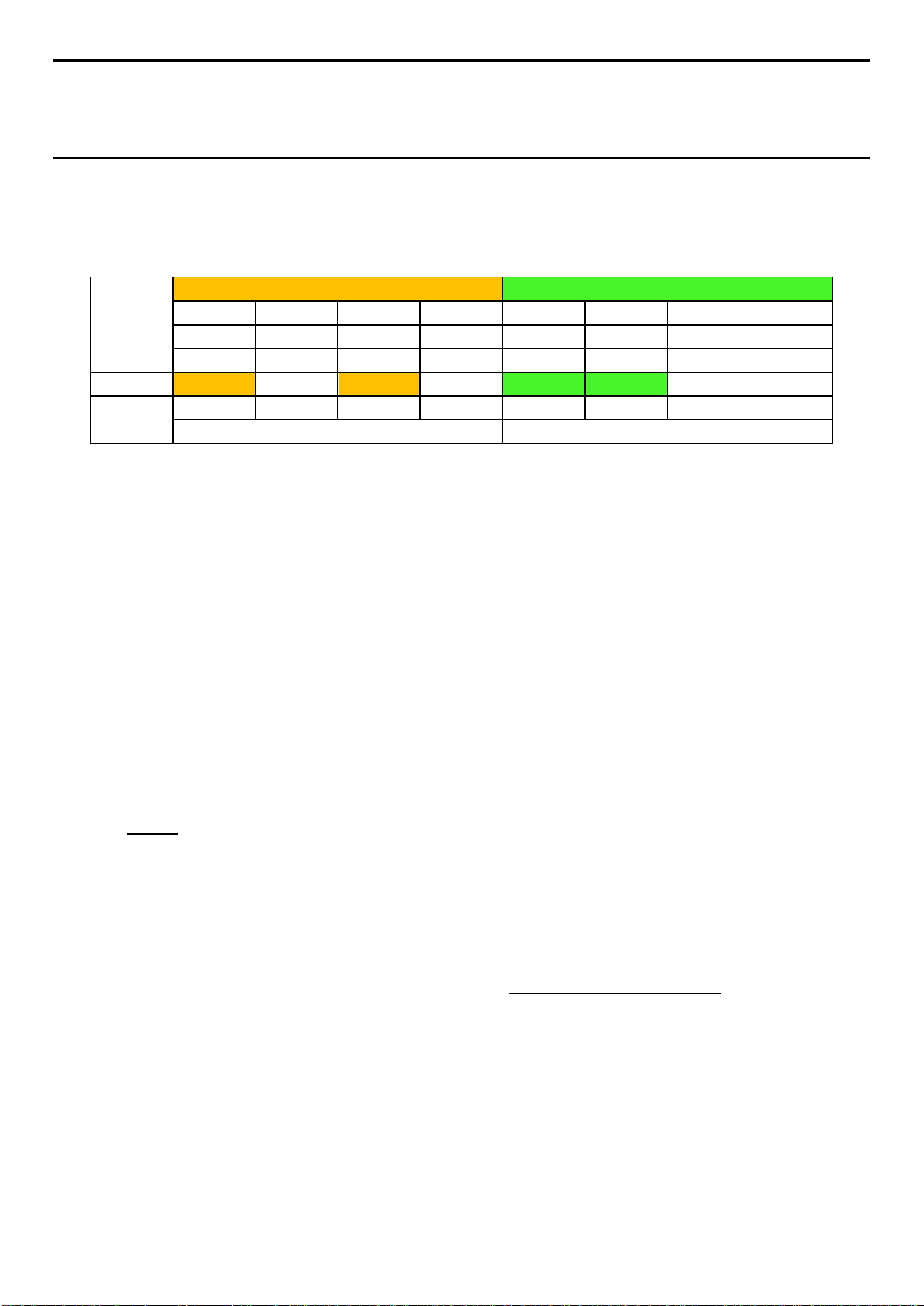
Upper Nibble AMBER LEDs
Lower Nibble GREEN LEDs
MSB
LSB
LED #7
LED #6
LED #5
LED #4
LED #3
LED #2
LED #1
LED #0
8h
4h
2h
1h
8h
4h
2h
1h
ON
OFF
ON
OFF
ON
ON
OFF
OFF
1 0 1 0 1 1 0 0 Ah
Ch
NOTE: All POST Diagnostic codes must be read from left to right starting from MSB to LSB in given
numerical order (7-6-5-4-3-2-1-0) when user is facing the back of the system as shown in Error!
Reference source not found.
. Failing to follow this instruction will result on a wrong
interpretation.
In the following example, the BIOS sends a value of ACh to the diagnostic LED decoder.
The LEDs are decoded as follows:
Table 9. POST Progress Code Decoding LED Example
LEDs
Status
Results
Upper nibble bits = 1010b = Ah; Lower nibble bits = 1100b = Ch; the two are concatenated as ACh
Early POST Memory Initialization MRC Diagnostic Codes
Memory Initialization at the beginning of POST includes multiple functions, including: discovery, channel
training, validation that the DIMM population is acceptable and functional, initialization of the IMC and
other hardware settings, and initialization of applicable RAS configurations.
Below is a brief list of the Diagnostic LED codes displayed during memory initialization by the Memory
Reference Code (MRC), the BIOS component responsible for it. There are two types of POST Diagnostic
Codes used by the MRC, Fatal Error Codes and Progress Codes.
MRC Fatal Error Codes are necessary because if the Memory Initialization fails badly for some reason – like
no usable memory installed – the system would not have the resources to give any other error indication.
So in the case of a major failure during Memory Initialization, the system outputs a Fatal Error Code to Port
80 (the Diagnostic LEDs) and executes a Halt. These Fatal Error Halts do not change the System Status LED,
and they do not get logged as SEL Events.
The MRC Progress Codes are displays to the Diagnostic LEDs that show the execution point in the MRC
operational path at each step. The intent is that if the system hangs during execution of the MRC, the LED
display will tell at what point in the code the system was executing.
Be aware that these are Diagnostic LED display codes used in early POST by the MRC. Later in POST, these
same Diagnostic LED display codes are used for other BIOS Progress Codes.
Also, MRC Fatal Error Codes and MRC Progress Codes are not controlled by the BIOS and are subject to
change based upon changes implemented in the memory reference code.
Page 85

Error Code
Fatal Error Code Explanation (with MRC Internal Minor Code)
0xE8
No Usable Memory Error:
0xE9
Memory is locked by Intel® Trusted Execution Technology and is inaccessible.
0xEA
DDR4 Channel Training Error:
0xEB
Memory Test Failure:
0xED
DIMM Configuration/Population Error:
0xEF
Indicates a CLTT table structure error.
Table 10. MRC Fatal Error Codes
01h = No memory was detected via SPD read, or invalid config that causes no operable
memory.
02h = Memory DIMMs on all channels of all sockets are disabled due to hardware memtest
er ro r.
03h = No memory installed. All channels are disabled.
01h = Error on read DQ/DQS (Data/Data Strobe) init
02h = Error on Receive Enable
03h = Error on Write Leveling
04h = Error on write DQ/DQS (Data/Data Strobe)
01h = Software memtest failure.
02h = Hardware memtest failed.
03h = Hardware Memtest failure in Lockstep Channel mode requiring a channel to be disabled.
This is a fatal error which requires a reset and calling MRC with a different RAS mode to retry.
01h = Different DIMM types (RDIMM, LRDIMM) are detected installed in the system.
02h = Violation of DIMM population rules.
03h = The third DIMM slot cannot be populated when QR DIMMs are installed.
04h = UDIMMs are not supported.
05h = Unsupported DIMM Voltage.
Should a major memory initialization error occur, preventing the system from booting with data integrity, a
beep code is generated, the MRC will display a fatal error code on the diagnostic LEDs, and a system halt
command is executed. Fatal MRC error halts do NOT change the state of the System Status LED, and they
do NOT get logged as SEL events. The following table lists all MRC fatal errors that are displayed to the
Diagnostic LEDs.
NOTE: Fatal MRC errors will display POST error codes that may be the same as BIOS POST progress
codes displayed later in the POST process. The fatal MRC codes can be distinguished from the BIOS
POST progress codes by the accompanying memory failure beep code of 3 long beeps.
Table 14
Page 86

Progress Code
Main Sequence
Subsequences/Subfunctions
the JEDEC defined initialization
Table 11. MRC Progress Codes
0xB0 Detect DIMM population
0xB1 Set DDR4 frequency
0xB2 Gather remaining SPD data
0xB3 Program registers on the memory controller level
0xB4 Evaluate RAS modes and save rank information
0xB5 Program registers on the channel level
0xB6 Perform
sequence
0xB7 Train DDR4 ranks
0x01
—n/a—
—n/a—
—n/a—
—n/a—
—n/a—
—n/a—
—n/a—
—n/a—
Read DQ/DQS training
0x02
0x03
0x04
0x05
0xB8 Initialize CLTT/OLTT
0xB9 Hardware memory test and init
0xBA Execute software memor y init
0xBB Program memory map and interleaving
0xBC Program RAS configuration
0xBF MRC is done
Receive Enable training
Write Leveling training
Write DQ/DQS training
DDR channel training done
—n/a—
—n/a—
—n/a—
—n/a—
—n/a—
—n/a—
Page 87

SEC Phase
First POST code after CPU reset
Microcode load begin
CRAM initialization begin
Pei Cache When Disabled
SEC Core At Power On Begin.
Early CPU initialization during Sec
Early SB initialization during Sec Phase.
Early NB initialization during Sec
End Of Sec Phase.
Microcode Not Found.
Microcode Not Loaded.
PEI Core
CPU PEIM
NB PEIM
SB PEIM
MRC Progress Codes
Memory Installed
CPU PEIM (CPU Init)
BIOS POST Progress Codes
During the system boot process, the BIOS executes a number of platform configuration processes, each of
which is assigned a specific POST Progress Code, a 2-digit hexadecimal number. As each configuration
routine is started, the BIOS displays the POST Progress Code on the Diagnostic LEDs found on the back
edge of the server board.
To assist in troubleshooting a system hang during the POST process, the POST Progress Code displayed in
the Diagnostic LEDs can be used to identify the last POST process to begin execution.
The following table provides a list of all POST progress codes.
Table 12. POST Progress Codes
Progress Code Description
0x01
0x02
0x03
0x04
0x05
0x06
0x07
0x08
0x09
0x0E
0x0F
0x10
0x11
Phase.
Phase.
PEI Phase
0x15
0x19
At this point the MRC Progress Code sequence is executed
See Error! Reference source not found..
0x31
0x32
Page 88

CPU PEIM (Cache Init)
Dxe IPL started
DXE Core started
DXE NVRAM Init
DXE Setup Init
DXE CPU Init
DXE CPU BSP Select
DXE CPU AP Init
DXE PCI Host Bridge Init
DXE NB Init
DXE NB SMM Init
DXE SB Init
DXE SB SMM Init
DXE SB devices Init
DXE ACPI Init
DXE CSM Init
DXE BDS Started
DXE BDS connect drivers
DXE PCI Bus begin
DXE PCI Bus HPC Init
DXE PCI Bus enumeration
DXE PCI Bus resource requested
DXE PCI Bus assign resource
DXE CON_OUT connect
DXE CON_IN connect
DXE SIO Init
Progress Code Description
0x33
0x4F
DXE Phase
0x60
0x61
0x62
0x63
0x65
0x66
0x68
0x69
0x6A
0x70
0x71
0x72
0x78
0x79
0x80
0x81
0x82
0x83
0x84
0x85
0x86
0x87
0x88
0x89
Page 89

DXE USB start
DXE USB reset
DXE USB detect
DXE USB enable
DXE IDE begin
DXE IDE reset
DXE IDE detect
DXE IDE enable
DXE SCSI begin
DXE SCSI reset
DXE SCSI detect
DXE SCSI enable
DXE verifying SETUP password
DXE SETUP start
DXE SETUP input wait
DXE Ready to Boot
DXE Legacy Boot
DXE Exit Boot Services
RT Set Virtual Address Map Begin
DXE Legacy Option ROM init
DXE Reset system
DXE USB Hot plug
DXE PCI BUS Hot plug
DXE NVRAM cleanup
DXE ACPI Enable
Clear POST Code
S3 Resume
Progress Code Description
0x8A
0x8B
0x8C
0x8D
0x91
0x92
0x93
0x94
0x95
0x96
0x97
0x98
0x99
0x9B
0x9C
0x9D
0x9E
0x9F
0xC0
0xC2
0xC3
0xC4
0xC5
0xC6
0xC7
0x00
Page 90

S3 Resume PEIM (S3 started)
S3 Resume PEIM (S3 boot script)
S3 Resume PEIM (S3 Video Repost)
S3 Resume PEIM (S3 OS wake)
PEIM which detected forced Recovery
PEIM which detected User Recover y
Recovery PEIM (Recovery started)
Recovery PEIM (Capsule found)
Recovery PEIM (Capsule loaded)
Progress Code Description
0x40
0x41
0x42
0x43
BIOS Recovery
0x46
0x47
0x48
0x49
0x4A
condition
condition
Page 91

Error Code
Error Message
Response
0012
System RTC date/time not set
Major
0048
Password check failed
Major
0140
PCI component encountered a PERR error
Major
0141
PCI resource conflict
Major
0146
PCI out of resources error
Major
5220
BIOS Settings reset to default settings
Major
5221
Passwords cleared by jumper
Major
5224
Password clear jumper is Set
Major
8130
Processor 01 disabled
Major
8160
Processor 01 unable to apply microcode update
Major
8170
Processor 01 failed Self-Test (BIST)
Major
8180
Processor 01 microcode update not found
Minor
8190
Watchdog timer failed on last boot
Major
Appendix C. POST Error Codes
Most error conditions encountered during POST are reported using POST Error Codes. These codes
represent specific failures, warnings, or are informational. POST Error Codes may be displayed in the Error
Manager display screen, and are always logged to the System Event Log (SEL). Logged events are available
to System Management applications, including Remote and Out of Band (OOB) management.
There are exception cases in early initialization where system resources are not adequately initialized for
handling POST Error Code reporting. These cases are primarily Fatal Error conditions resulting from
initialization of processors and memory, and they are handed by a Diagnostic LED display with a system
halt.
The following table lists the supported POST Error Codes. Each error code is assigned an error type which
determines the action the BIOS will take when the error is encountered. Error types include Minor, Major,
and Fatal. The BIOS action for each is defined as follows:
Minor: The error message is displayed on the screen or on the Error Manager screen, and an error is logged
to the SEL. The system continues booting in a degraded state. The user may want to replace the erroneous
unit. The POST Error Pause option setting in the BIOS setup does not have any effect on this error.
Major: The error message is displayed on the Error Manager screen, and an error is logged to the SEL. The
POST Error Pause option setting in the BIOS setup determines whether the system pauses to the Error
Manager for this type of error so the user can take immediate corrective action or the system continues
booting.
Note that for 0048 “Password check failed”, the system halts, and then after the next reset/reboot will
display the error code on the Error Manager screen.
Fatal: The system halts during POST at a blank screen with the text “Unrecoverable fatal error found.
System will not boot until the error is resolved” and “Press <F2> to enter Setup” The POST Error Pause
option setting in the BIOS setup does not have any effect with this class of error.
When the operator presses the F2 key on the keyboard, the error message is displayed on the Error
Manager screen, and an error is logged to the SEL with the error code. The system cannot boot unless the
error is resolved. The user needs to replace the faulty part and restart the system.
NOTE: The POST error codes in the following table are common to all current generation Intel server
platforms. Features present on a given server board/system will determine which of the listed error codes
are supported.
Table 13. POST Error Codes and Messages
Page 92

Error Code
Error Message
Response
8198
OS boot watchdog timer failure
Major
8300
Baseboard management controller f ai led sel f-test
Major
8305
Hot Swap Controller failure
Major
83A0
Management Engine (ME) failed self-test
Major
83A1
Management Engine (ME) Failed to respond.
Major
84F2
Baseboard management controller failed to respond
Major
84F3
Baseboard management controller in update mode
Major
84F4
Sensor data record empty
Major
84FF
System event log full
Minor
8500
Memory component could not be configured in the selected RAS mode
Major
8501
DIMM Population Error
Major
8520
DIMM_A1 failed test/initialization
Major
8523
DIMM_B1 failed test/initialization
Major
8526
DIMM_C1 failed test/initializ ati on
Major
8529
DIMM_D1 failed test/initializ ati on
Major
852C
DIMM_E1 failed test/initialization
Major
852F
DIMM_F1 failed test/initialization
Major
8540
DIMM_A1 disabled
Major
8543
DIMM_B1 disabled
Major
8546
DIMM_C1 disabled
Major
8549
DIMM_D1 disabled
Major
854C
DIMM_E1 disabled
Major
854F
DIMM_F1 disabled
Major
8560
DIMM_A1 encountered a Serial Presence Detection (SPD) failure
Major
8563
DIMM_B1 encountered a Serial Presence Detection (SPD) failure
Major
8566
DIMM_C1 encountered a Serial Presence Detection (SPD) failure
Major
8569
DIMM_D1 encountered a Serial Presence Detection (SPD) failure
Major
856C
DIMM_E1 encountered a Serial Presence Detection (SPD) failure
Major
856F
DIMM_F1 encountered a Serial Presence Detection (SPD) failure
Major
8604
POST Reclaim of non-crit i cal NVR AM variables
Minor
8605
BIOS Settings are corrupted
Major
8606
NVRAM variable space was corrupted and has been reinitialized
Major
Recovery boot has been initiated.
Fatal
92A3
Serial port component was not detected
Major
92A9
Serial port component encountered a resourc e confl ict error
Major
A000
TPM device not detected.
Minor
A001
TPM device missing or not responding.
Minor
A002
TPM device failure.
Minor
A003
TPM device failed self-test.
Minor
A100
BIOS ACM Error
Major
A421
PCI component encountered a SERR error
Fatal
A5A0
PCI Express component encountered a PERR error
Minor
A5A1
PCI Express component encountered an SERR error
Fatal
DXE Boot Services driver: Not enough memory available to shadow a Legacy
Minor
8607
A6A0
Note: The Primary BIOS image may be corrupted or the system may hang during
POST. A BIOS update is required.
Option ROM.
Page 93

Beeps
Error Message
POST Progress Code
Description
1
USB device action
N/A
Short beep sounded whenever USB device is
1 long
Intel® TXT security
0xAE, 0xAF
System halted because Intel® Trusted Execution
3
Memory error
Multiple
System halted because a fatal error related to the
3 long
CPU mismatch
0xE5, 0xE6
System halted because a fatal error related to the
The following Beep Codes are sounded during BIOS Recovery.
2
Recovery started
N/A
Recovery boot has been initiated.
4
Recovery failed
N/A
Recovery has failed. This typically happens so quickly
1-5-2-1
CPU socket
N/A
CPU1 socket is empty, or sockets are populated
1-5-2-4
MSID Mismatch
N/A
MSID mismatch occurs if a processor is installed into
1-5-4-2
Power fault
N/A
DC power unexpectedly lost (power good dropout) –
1-5-4-4
Power control
N/A
Power good assertion timeout – Power unit sensors
1-5-1-2
VR Watchdog
N/A
VR controller DC power on sequence not completed
1-5-1-4
Power Supply
N/A
The system does not power on or unexpectedly
POST Error Beep Codes
The following table lists POST Error Beep Codes. Prior to system video initialization, the BIOS uses these
beep codes to inform users of error conditions. The beep code is followed by a user visible code displayed
on the Diagnostic LEDs.
The following tables lists POST Error Beep Codes. Prior to system video initialization, the BIOS uses these
beep codes to inform users of error conditions. The beep code is followed by a user visible code displayed
on the Diagnostic LEDs.
Table 14. POST Error Beep (with LED) Codes
discovered in POST, or inserted or removed during
runtime.
violation
and 1
error
The following beep codes are generated by the BMC.
Table 15. Integrated BMC Beep (with LED) Codes
population error
Technology detected a potential violation of system
security.
memory was detected.
CPU family/core/cache mismatch was detected.
after recovery is initiated that it sounds like a 2-4
beep code.
incorrectly – CPU1 must be populated before CPU2.
a system board that has incompatible power
capabilities.
fault
Timer
Status
Power unit sensors report power unit failure offset.
report soft power control failure offset.
in time.
powers off and a Power Supply Unit (PSU) is present
that is an incompatible model with one or more other
PSUs in the system.
Page 94

Appendix D. System Interconnects S7200AP / H2000G
S7200AP / H2000G (12x3.5” Drive Configuration) and system interconnect
Figure 92. System Interconnect
Page 95

Appendix E. Regulatory and Compliance Information
Refer to the Server Products Regulatory and Safety document for the product regulatory compliance
reference. The document can be downloaded from http://www.intel.com/support/server.
Page 96

Appendix F. Getting Help
If you encounter an issue with your compute module, follow these steps to obtain support:
1. Visit the following Intel support web page:
http://www.intel.com/p/en_US/support/contactsupport
This web page provides 24x7 support when you need it to get the latest and most complete technical
support information on all Intel Enterprise Server and Storage Platforms. Information available at the
support site includes:
Latest BIOS, firmware, drivers, and utilities
Product documentation, installation and quick start guides
Full product specifications, technical advisories, and errata
Compatibility documentation for memory, hardware Add-In Cards, chassis support matrix, and
operating systems
Server and chassis accessory parts list for ordering upgrades or spare parts
A searchable knowledgebase to search for product information throughout the support site
2. If you are still unable to obtain a solution to your issue, send an email to Intel’s technical support center
using the online form available at http://www.intel.com/support/feedback.htm?group=server.
Lastly, you can contact an Intel support representative using one of the support phone numbers
available at http://www.intel.com/support/feedback.htm?group=server (charges may apply).
Intel also offers Channel Program members around-the-clock 24x7 technical phone support on Intel’s
Server Boards, Server Chassis, Server RAID Controller Cards, and Intel Server Management at
http://www.intel.com/reseller/.
NOTE: You will need to log in to the Reseller site to obtain the 24x7 number.
Warranty Information
To obtain warranty information, visit the following Intel web site:
http://www.intel.com/p/en_US/support/warranty
Page 97

Boot strap processor. The processor selected at boot time to be the primary processor in a multi-processor
system.
Dual In-line Memory Module, a plug-in memory module with signal and power pins on both sides of the
Keyboard, Video, and Mouse – an attachment that mimics those devices, and connects them to a remote I/O
user
Glossary
Acronym Description
AC Alternating Current, a type of electrical current in which the current repeatedly changes direction
ACM Authenticated Code Mode
ACPI Advanced Configuration Power Interface
AP Application Processor
BDS Boot Device Selection
BIB Burn in Board
BIOS Basic Input/Output System – Firmware interface to the system hardware
BIST Built-in Self-Test
BMC Baseboard Management Controller
BSP
BTU/hour A unit of power. 1 watt is approximately 3.41214 BTU/h[, and 1000 BTU/h is approximately 293.071 W
CLT T Closed Loop Thermal Throttling
CMOS Complementary Metal-oxide-semiconductor
CPU Central Processing Unit
CRAM
CSM Compatibility Support Module
DC Direct current, the flow of electric charge is only in one direction.
DIMM
DQ Data Quality
DQS Bi-directional Data Strobe
DXE Driver Execution Environment. Component of Intel® Platform Innovation Framework for EFI architecture
EI Enhanced Intel
ESD Electrostatic Discharge
FRU Field Replaceable Unit
GT/s GigaTransfers per second
HBA Hot Bus Adapter
HPC High Performance Computing
IDE Integrated Drive Electronics, a disk interface standard
Configuration RAM - a programmable bit inside an FPGA that controls its behavior
internal printed circuit board (front and back).
IFT Intel Fabric Through
IMC Integrated Memory Controller – memory controller integrated into the processor chip
IPL Initial Program Load
IPMB Intelligent Platform Management Bus
ISTA International Safe Transit Association
JEDEC Joint Electron Device Engineering Council, industry organization for memory standards
KVM
LAN Local Area Network
LED Light Emitting Diode
Page 98

Acronym Description
Load Reduced DIMM memor y modules have buffer registers for both address and data between the SDRAM
modules and the system's memory controller.
Redundant Array of Inexpensive Disks – provides data security by spreading data over multiple disk drives.
Registered DIMM (also called buffered) memory modules have an address buffer register between the SDRAM
modules and the system's memory controller.
LOM LAN on Board
LRDIMM
ME Management Engine
MM# Material Management number
MRC Memory Reference Code
MSB Most Significant Bit
MSID
MT/s MegaTransfers per second
NB
NIC Network Interface Card
NVRAM Non-volatile RAM
OEM Original Equipment Manufacturer
OFU One-Boot Flash Update
OLT T Open Loop Thermal Throttling
OOB Out of Band
OS Operating System
PCH
PCI Peripheral Component Interconnect, or PCI Local Bus Standard – also called “Conventional PCI”
PCIe** PCI Express* -- an updated form of PCI offering better throughput and better error management
PEI Pre EFI Initialization. Component of Intel® Platform Innovation Framework for EFI architecture.
PEIM PEI Module
PERR Parity Error
CPU Icc Mismatch
Northbound
Platform Controller Hub
PHM Processor Heatsink Module
POST Power On Self-Tes t – BIOS activity from the time on Power On until Operating System boot begins.
PSU Power Supply Unit
QPI Intel® QuickPath Interconnect
QR Quad Rank – memory DIMM organization, DRAMs organized in four ranks
RAID
RAM Random Access Memory
RAS Reliability, Availability, and Serviceability
RC Raw Class
RDIMM
ROM
RT Runtime. Component of Intel® Platform Innovation Framework for EFI architecture
RTC Real Time Clock
SAD Source Address Decoder
SAS Serial Attached SCSI, a high speed serial data version of SCSI
RAID 0, RAID 1, RAID 10, and RAID 5 are different patterns of data on varying numbers of disks to provide
varying degrees of security and performance.
Read-Only Memor y
SATA Serial ATA, a high speed serial data version of the disk ATA interface
Page 99

The enhanced small form-factor pluggable (SFP+) is an enhanced version of the SFP that supports data rates
up to 16 Gbit /s.
Acronym Description
SB Southbound
SBSP System Boot-Strap Processor
SCSI Small Computer System Interface, a connection usually used for disks of various types
SDR Sensor Data Record
SEC Security. Component of Intel® Platform Innovation Framework for EFI architecture
SEL System Event Log
SERR System Error
SFF Small Form Factor
SFP+
SIO Super I/O
SMM System Management Mode
SPD Serial Presence Detect
SUP System Updated Package
TDP Thermal Design Power
TIM Thermal Interface Material
TPM Trusted Platform Module
TXT Intel® Trusted Execution Technology
USB Universal Serial Bus, a standard serial expansion bus meant for connecting peripherals.
VGA
VR Voltage Regulator
Video Graphics Array
 Loading...