

Page 1

GD82559ER Fast Ethernet**
PCI Controller
Networking Silicon
Product Features
Datasheet
■ Optimum Integration for Lowest Cost
Solution
—Integrated IEEE 802.3 10BASE-T and
100BASE-TX compatible PHY
—Glueless 32-bit PCI master interface
—128 Kbyte Flash interface
—Thin BGA 15mm
—ACPI and PCI Power Management
—Power management e v en t on
“interesting” packets and link status
change support
—Test Access Port
2
package
■ High Performance Networking Functions
—Chained memory structure similar to the
82559,82558, 82557, and 82596
—Improved dynamic transmit chaining
with multiple priorities transmit queues
—Full Duplex support at both 10 and 100
Mbps
—IEEE 802.3u Auto-Negotiation support
—3 Kbyte transmit and 3 Kbyte receive
FIFOs
—Fast back-to-back transmission support
with minimum interframe spacing
—IEEE 802.3x 100BASE-TX Flow
Control support
—Low Power Features
—Low power 3.3 V device
—Efficient dynamic stan dby mode
—Deep power down support
—Clockrun protocol support
Document Number: 714682-001
Revision 1.0
March 1999
Page 2

GD82559ER - Networking Silicon
Revision History
Revision
Date
Revision Description
Mar. 1999 1.0 First release.
Information in this document is provided in connection with Intel products. No license, express or implied, by estoppel or otherwise, to any intellectual
property rights is granted by this document. Except as provided in Intel's Terms and Conditions of Sale for such products, Intel assumes no liability
whatsoever, and Intel disclaims any express or implied warranty, relating to sale and/or use of Intel products including liability or warranties relating to
fitness for a particular purpose, merchantability, or infringement of any patent, copyright or other intellectual property right. Intel products are not
intended for use in medical, life saving, or life sustaining applications.
Intel may make changes to specifications and product descriptions at any time, without notice.
Designers must not rely on the absence or characteristics of any features or instructions marked "reserved" or "undefined." Intel reserves these for
future definition and shall have no responsibility whatsoever for conflicts or incompatibilities arising from future changes to them.
The 82559 may contain design defects or errors known as errata which may cause the product to deviate from published specifications. Current
characterized errata are available on request.
Contact your local Intel sales office or your distributor to obtain the latest specifications and before placing your product order.
Copyright © Intel Corporation, 1999
* Alert on LAN is a result of the Intel-IBM Advanced Manageability Alliance and a trademark of IBM.
** Third-party brands and names are the property of their respective owners.
ii
Datasheet
Page 3

Networking Silicon — GD82559ER
Contents
1. INTRODUCTION .............................................................................................................................1
1.1 GD82559ER Overview .......................................................................................................1
1.2 Suggested Reading ............................................................................................................1
2. GD82559ER ARCHITECTURAL OVERVIEW................................................................................3
2.1 Parallel Subsystem Overview... .......................................................... ....... ...... ....... ...... ......3
2.2 FIFO Subsystem Overview.................................................................................................4
2.3 10/100 Mbps Serial CSMA/CD Unit Overview....................................................................5
2.4 10/100 Mbps Physical Layer Unit.......................................................................................5
3. SIGNA L DESCRIP TIO NS .................................. ....... .......................................................... ...... . .....7
3.1 Signal Type Definitions.......................................................................................................7
3.2 PCI Bus Interface Signals...................................................................................................7
3.2.1 Address and Data Signals.................. ...... ....... ...................................................7
3.2.2 Interface Control Signals ....................................................................................8
3.2.3 System and Power Management Signals...........................................................9
3.3 Local Memory Interface Signals.........................................................................................9
3.4 Testability Port Signals.....................................................................................................10
3.5 PHY Signals .....................................................................................................................11
4. GD82559ER MEDIA ACCESS CONTROL FUNCTIONAL DESCRIPTION.................................13
4.1 82559ER Initialization.......................................................................................................13
4.1.1 Initialization Effects on 82559ER Units ............................................................13
4.2 PCI Interface.....................................................................................................................14
4.2.1 82559ER Bus Operations.................................................................................14
4.2.2 Clockrun Signal ............... .......................................................... ...... ....... ...... ....2 2
4.2.3 Power Management Event Signal....................................................................22
4.2.4 Power States....................................................................................................23
4.2.5 Wake-up Events...............................................................................................27
4.3 Parallel Flash Interface............. ....... ...... ....... ...... ...... ....... ...... ....... ...... ..............................28
4.4 Serial EEPROM Interface.................................................................................................28
4.5 10/100 Mbps CSMA/CD Unit............................................................................................30
4.5.1 Full Duplex .......................................................................................................31
4.5.2 Flow Control .....................................................................................................31
4.5.3 Address Filtering Modifications.........................................................................31
4.5.4 Long Frame Reception.....................................................................................31
4.6 Media Independent Interface (MII) Management Interface...............................................32
5. GD82559ER TEST PORT FUNCTIONALITY...............................................................................33
5.1 Introduction.......................................................................................................................33
5.2 Asynchronous Test Mode.................................................................................................33
5.3 Test Function Description.................................................................................................33
5.4 85/85.................................................................................................................................33
5.5 TriState.............................................................................................................................34
5.6 Nand - Tree ......................................................................................................................34
6. GD82559ER PHYSICAL LAYER FUNCTIONAL DESCRIPTION................................................37
6.1 100BASE-TX PHY Unit ....................................................................................................37
6.1.1 100BASE-TX Transmit Clock Generation ........................................................37
Datasheet
iii
Page 4

GD82559ER — Networking Silicon
6.1.2 100BASE-TX Transmit Blocks .................... ....... ..............................................37
6.1.3 100BASE-TX Receive Blocks ............................ ...... ........................................40
6.1.4 100BASE-TX Collision Detection ................ ....... ...... ....... ...... ....... ...... ....... .......41
6.1.5 100BASE-TX Link Integrity and Auto-Negotiati on Sol ution.......... ...... ....... ...... .41
6.1.6 Auto 10/100 Mbps Speed Selection.................................................................41
6.2 10BASE-T Functionality ...................................................................................................41
6.2.1 10BASE-T Transmit Clock Generation.............................................................41
6.2.2 10BASE-T Transmit Blocks..............................................................................42
6.2.3 10BASE-T Receive Blocks...............................................................................42
6.2.4 10BASE-T Collision Detection..........................................................................43
6.2.5 10BASE-T Link Integrity...................................................................................43
6.2.6 10BASE-T Jabber Control Function.................................................................43
6.2.7 10BASE-T Full Duplex .....................................................................................43
6.3 Auto-Negotiation Functionalit y.................................................. ....... ...... ....... ....................43
6.3.1 Description ...................................... ...... ...... .....................................................44
6.3.2 Parallel Detect and Auto-Negotiation...............................................................44
6.4 LED Description................................................................................................................45
7. PCI CONFIGURATION REGISTERS ...........................................................................................47
7.1 LAN (Ethernet) PCI Configuration Space.........................................................................47
7.1.1 PCI Vendor ID and Device ID Registers ..........................................................47
7.1.2 PCI Command Register ...................................................................................48
7.1.3 PCI Status Register..........................................................................................49
7.1.4 PCI Revision ID Register..................................................................................50
7.1.5 PCI Class Code Register .................................................................................50
7.1.6 PCI Cache Line Size Register..........................................................................50
7.1.7 PCI Latency Timer............................................................................................51
7.1.8 PCI Header Type..............................................................................................51
7.1.9 PCI Base Address Registers............................................................................51
7.1.10 PCI Subsystem Vendor ID and Subsystem ID Registers.................................53
7.1.11 Capability Pointer .............................................................................................53
7.1.12 Interrupt Line Register......................................................................................53
7.1.13 Interrupt Pin Register .......................................................................................54
7.1.14 Minimum Grant Register ..................................................................................54
7.1.15 Maximum Latency Register..............................................................................54
7.1.16 Capability ID Register.......................................................................................54
7.1.17 Next Item Pointer......... ....... ...... ....... .......................................................... ...... .54
7.1.18 Power Management Capabilities Register.......................................................54
7.1.19 Power Management Control/Status Register (PMCSR)...................................55
7.1.20 Data Register ...................................................................................................56
8. CONTROL/STATUS REGISTERS................................................................................................57
8.1 LAN (Ethernet) Control/Status Registers..........................................................................57
8.1.1 System Control Block Status Word..................................................................58
8.1.2 System Control Block Command Word............................................................59
8.1.3 System Control Block General Pointer.............................................................59
8.1.4 PORT ...............................................................................................................59
8.1.5 Flash Control Register......................................................................................59
8.1.6 EEPROM Control Register...............................................................................59
8.1.7 Management Data Interface Control Register..................................................59
8.1.8 Receive Direct Memory Access Byte Count.....................................................60
8.1.9 Early Receive Interrupt.....................................................................................60
iv
Datasheet
Page 5

Networking Silicon — GD82559ER
8.1.10 Flow Control Register.......................................................................................60
8.1.11 Power Management Driver Register................................................................60
8.1.12 General Control Register..................................................................................61
8.1.13 General Status Register...................................................................................61
8.2 Statistical Counters...........................................................................................................62
9. PHY UNIT REGISTERS................................................................................................................65
9.1 MDI Registers 0 - 7............. ...... ....... ...... .......................................................... ....... ...... .. ..6 5
9.1.1 Register 0: Control Register Bit Definitions .....................................................65
9.1.2 Register 1: Status Register Bit Definitions .......................................................66
9.1.3 Register 2: PHY Identifier Register Bit Definitions ...........................................67
9.1.4 Register 3: PHY Identifier Register Bit Definitions ...........................................67
9.1.5 Register 4: Auto-Negotiation Advertisement Register Bit Definitions ..............67
9.1.6 Register 5: Auto-Negotiation Link Partner Ability Register Bit Definitions .......67
9.1.7 Register 6: Auto-Negotiation Expansion Register Bit Definitions ....................68
9.2 MDI Registers 8 - 15........... ...... ....... ...... .......................................................... ....... ...... ... .68
9.3 MDI Register 16 - 31 ... ....... ...... ....... ...... .......................................................... ....... ...... ....68
9.3.1 Register 16: PHY Unit Status and Control Register Bit Definitions .................68
9.3.2 Register 17: PHY Unit Special Control Bit Definitions .....................................69
9.3.3 Register 18: PHY Address Register.................................................................70
9.3.4 Register 19: 100BASE-TX Receive False Carrier Counter Bit Definitions ......70
9.3.5 Register 20: 100BASE-TX Receive Disconnect Counter Bit Definitions .........70
9.3.6 Register 21: 100BASE-TX Receive Error Frame Counter Bit Definitions ........70
9.3.7 Register 22: Receive Symbol Error Counter Bit Definitions ............................70
9.3.8 Register 23: 100BASE-TX Receive Premature End of Frame Error Counter
Bit Definitions ..................................................................................................71
9.3.9 Register 24: 10BASE-T Receive End of Frame Error Counter Bit Definitions .71
9.3.10 Register 25: 10BASE-T Transmit Jabber Detect Counter Bit Definitions ........71
9.3.11 Register 26: Equalizer Control and Status Bit Definitions ................................71
9.3.12 Register 27: PHY Unit Special Control Bit Definitions .....................................71
10. ELECTRICAL AND TIMING SPECIFICATIONS ..........................................................................73
10.1 Absolute Maximum Ratings..............................................................................................73
10.2 DC Specifications ............................................................................................................73
10.3 AC Specifications ............... ...... ....... ...... ....... ...... ...... ........................................................76
10.4 Timing Specifications........................................................................................................77
10.4.1 Clocks Specifications .......................................................................................77
10.4.2 Timing Parameters ...........................................................................................78
12. PACKAGE AND PINOUT INFORMATION...................................................................................85
12.1 Package Information.........................................................................................................85
12.2 Pinout Information ............................................................................................................86
12.2.1 GD82559ER Pin Assignments ........................................................................86
12.2.2 GD82559ER Ball Grid Array Diagram .............................................................88
Datasheet
v
Page 6

GD82559ER — Networking Silicon
vi
Datasheet
Page 7

g
1. Introduction
g
1.1 GD82559ER Overview
The 82559ER is part of Intel's second generation family of fully integrated 10BASE-T/100BASETX LAN solutions. The 82559ER consists of both the Media Access Controller (MAC) and the
physical layer (PHY) combined into a single component solution. 82559 family members build on
the basic functionality of the 82558 and contain power management enhancements.
The 82559ER is a 32-bit PCI controller that features enhanced scatter-gather bus mastering
capabilities which enables the 82559ER to perform high-speed data transfers over the PCI bus.The
82559ER bus master capabilities enable the compo nent to process high-level commands and
perform multiple operations, thereby off-loading communication tasks from the system CPU. Two
large transmit and receive FIFOs of 3 Kbytes each help prevent data underruns and overruns,
allowing the 82559ER to transmit data with minimum interframe spacing (IFS).
The 82559ER can operate in either full duplex or half duplex mode. In full duplex mode the
82559ER adheres to the IEEE 802.3x Flow Control specification. Half duplex performance is
enhanced by a proprietary collision reductio n mechanism.
Networkin
Silicon — GD82559ER
The 82559ER includes a simple PHY interface to the wire transformer at rates of 10BASE-T and
100BASE-TX, and Auto-Negotiation capability for speed, duplex, and flow con trol. These features
and others reduce cost, real estate, and design complexity.
The 82559ER also includes an interface to a serial (4-pin) EEPROM and a parallel interface to a
128 Kbyte Flash memory. The EEPROM provides power-on initialization for hardware and
software configuration parameters
1.2 Suggested Readin
The 82559 family of devices are designed to be compliant with PC industry power management
initiatives. This includes the ACPI, PCI Power Management Specification, Network Device Class
specification, etc. See the following publicaitons for more information about these topics.
•
PCI Specification, PCI Special Interest Group.
•
Network Device Class Reference, Revision 1.0, In tel Corpor atio n, Micros oft Corp oration , and
Toshiba.
•
Advanced Configuration and Power Interface (ACPI) Specification, Intel Corporation,
Microsoft Corporation, Toshiba.
•
Advanced Power Management (APM) Specification, Intel Corporation and Microsoft
Corporation.
•
82559 Fast Ethernet Multifunction PCI/CardBus Controller Datasheet, Intel Corporation.
•
LAN On Motherboard (LOM) Design Guide Application Note (AP-391), Intel Corporation.
•
Test Access Port Applications Note (AP-393), Intel Corporation.
Datasheet
1
Page 8

GD82559ER — Networking Silicon
2
Datasheet
Page 9
Networkin
g
g
(
)
g
(
)
y
y
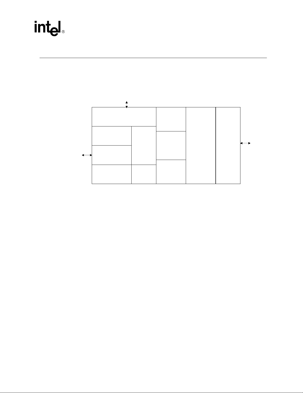
2. GD82559ER Architectural Overview
Figure 1 is a high level block diagram of the 82559ER. It is divided into four main subsystems: a
parallel subsystem, a FIFO subsystem, the 10/100 Mbps Carrier-Sense Multiple Access with
Collision Detect (CSMA/CD) unit, and the 10/10 0 Mbps physical layer (PHY) unit.
Local Memory
Interface
Silicon — GD82559ER
PCI Target and
Flash/EEPROM
Interface
PCI
Interface
Four Channel
Addressin
Interface Unit
Data Interface Unit
DMA
PCI Bus
BIU
DIU
Unit -
Micro-
machine
Dual
Ported
FIFO
Fi
ure 1. 82559ER Block Diagram
FIFO Control
2.1 Parallel Subsystem Overview
The parallel subsystem is broken down into several functional blocks: a PCI bus master interface, a
micromachine processing unit and its corresponding microcode ROM, and a PCI Target Control/
Flash/EEPROM interface. The parallel subsystem also interfaces to the FIFO subsystem, passing
data (such as transmit, receive, and configuration data) and command and status parameters
between these two blocks.
The PCI bus master interface provides a complete glueless interface to a PCI bus and is compliant
with the PCI Bus Specification, Revision 2.2. The 82559ER provides 32 bits of addressing and
data, as well as the complete control interface to operate on a PCI bus. As a PCI target, it follows
the PCI configuration format which allows all accesses to the 82559ER to be automatically
mapped into free memory and I/O space upon initialization of a PCI system. For processing of
transmit and receive frames, the 82559ER operates as a master on the PCI bus, initiating zero wait
state transfers for accessing these data parameters.
3 Kb
te
Tx FIFO
te
3 Kb
Rx FIFO
10/100 Mbps
CSMA/CD
100BASE-TX/
10BASE-T
PHY
TPE
Interface
The 82559ER Control/Status Register Block is part of the PCI target element. The Control/Status
Register block consists of the following 82559ER internal control registers: System Control Block
(SCB), PORT, Flash Control, EEPROM Control, and Management Data Interface (MDI) Control.
The micromachine is an embedded processing unit contained in the 82559ER. The micromachine
accesses the 82559ER microcode ROM working its way through the opcodes (or instructions)
contained in the ROM to perform its function s. Parameters acce ssed from memory such as po inters
to data buffers are also used by the micromachine during the processing of transmit or receive
frames by the 82559ER. A typical micromachine function is to transfer a data buffer pointer field
to the 82559ER DMA unit for direct access to the data buffer. The micromachine is divided into
two units, Receive Unit and Command Unit which includes transmit functions. These two units
Datasheet
3
Page 10

GD82559ER — Networking Silicon
operate independently. Control is switched between the two units according to the microcode
instruction flow . The indepe ndence of the Receive and Command units in the micromachine allows
the 82559ER to interleave commands and receive incoming frames, with no real-time CPU
intervention.
The 82559ER contains an interface to an external Flash memory, and external serial EEPROM.
These two interfaces are multiplexed. The Flash interface, which could also be used to connect to
any standard 8-bit device, provides up to 128 Kbytes of addressing to the Flash. Both read and
write accesses are supported. The Flash may be used for remote boot functions, network statistical
and diagnostic s functions, and manage ment functions. The Fl ash is mapped into host system
memory (anywhere within the 32-bit memory address space) for software accesses. It is also
mapped into an available boot expansion ROM location during boot time of the system. More
information on the Flash interface is detailed in Section 4.3, “Parallel Flash Interface” on page 28.
The EEPROM is used to store relevant information for a LAN connection such as node address, as
well as board manufacturing and configuration information. Both read and write accesses to the
EEPROM are supported by the 82559ER. Information on the EEPROM interface is detailed in
Section 4.4, “Serial EEPROM Interface” on page 28.
2.2 FIFO Subsystem Overview
The 82559ER FIFO subsystem consists of a 3 Kbyte transmit FIFO and 3 Kbyte receive FIFO.
Each FIFO is unidirectional and independent of the other. The FIFO subsystem serves as the
interface between the 82559ER parallel side an d the serial CSMA/CD unit. It provides a temporary
buffer storage area for frames as they are either being received or transmitted by the 82559ER,
which improves performance:
•
Transmit frames can be queued within the transmit FIFO, allowing back-to-back transmission
within the minimum Interframe Spacing (IFS).
•
The storage area in the FIFO allows the 82559ER to withstand long PCI bus latencies without
losing incoming data or corrupting outgoing data.
•
The 82559ER transmit FIFO threshold allows the transmit start threshold to be tuned to
eliminate underruns while concurrent transmits are being performed (i.e. pending transmits
will not be affected by the change in FIFO threshold).
•
The FIFO subsection allows extended PCI burst accesses with zero wait states to or from the
82559ER for both transmit and receive frames. This is because such the transfer is to the FIFO
storage area, rather than directly to the serial link.
•
Transmissions resulting in errors (collision detection or data underrun) are retransmitted
directly from the 82559ER FIFO, therey increasing performance and eliminating the need to
re-access this data from the host system.
•
Incoming runt receive frames (frames that are less than the legal minimum frame size) can be
discarded automatically by the 82559ER without transferri ng this faulty data to the host
system, and without host intervention.
•
Bad Frames resolution can be selectively left to the 82559ER, or under software control.
4
Datasheet
Page 11

Networkin
g
2.3 10/100 Mbps Serial CSMA/CD Unit Overview
The CSMA/CD unit of the 82559ER all ows it t o be conn ect ed to either a 10 or 100 Mbps Ethern et
network. The CSMA/CD unit performs all of the functions of the 802.3 protocol such as frame
formatting, frame stripping, collision handling, deferral to link traf fic, etc. The CSMA/CD unit can
also be placed in a full-duplex mode, which allows simultaneous transmission and reception of
frames.
2.4 10/100 Mbps Physical Layer Unit
The Physical Layer (PHY) unit of the 82559ER allows connection to either a 10 or 100 Mbps
Ethernet network. The PHY unit supports Auto-Negotiation for 100BASE-TX Full Duplex,
100BASE-TX Half Duplex, 10BASE-T Full Duplex, and 10BASE-T Half Duplex. It also supports
three LED pins to indicate link status, network activity, and speed.The 82559ER does not support
external PHY devices and does not expose its internal MII bus.
Silicon — GD82559ER
Datasheet
5
Page 12

GD82559ER — Networking Silicon
6
Datasheet
Page 13

g
3. Signal Descriptions
g
y
g
y
g
g
y
g
g
g
y
y
y
y
g
g
y
g
g
y
y
y
y
g
3.1 Signal Type Definitions
Type Name Description
IN Input The input pin is a standard input onl
OUT Output
T/S Tri-State The tri-state pin is a bidirectional, input/output pin.
S/T/S Sustained Tri-State
O/D Open Drain
A/I Analo
A/O Analo
B Bias The bias pin is an input bias.
Input The analog input pin is used for analog input signals.
Output The analog output pin is used for analog output signals.
The output pin is a Tot em Pole Output pin and is a standard
active driver.
The sustained tri-state pin is an active low tri-state si
and driven b
S pin low must drive it hi
floatin
one clock c
owner.
The open drain pin allows multiple devices to share this si
as a wired-OR.
Networkin
one agent at a time. The agent asserting the S/T/
h at least one clock cycle before
the pin. A new agent can only assert an S/T/S signal low
cle after it has been tri-stated by the previous
Silicon —GD82559ER
signal.
nal owned
nal
3.2 PCI Bus Interface Si
3.2.1 Address and Data Signals
Symbol Type Name and Function
Address and Data.
the same PCI pins. A bus transaction consists of an address phase
followed b
AD[31:0] T/S
C/BE[3:0]# T/S
PAR T/S
address and data lines contain the 32-bit ph
this is a b
address. The 82559ER uses little-endian b
words, AD[31:24] contain the most si
contain the least si
and data lines contain data.
Command and Byte Enable.
nals are multiplexed on the same PCI pins. During the address
si
phase, the C/BE# lines define the bus command. Durin
phase, the C/BE# lines are used as B
are valid for the entire data phase and determine which b
meaningful data.
carr
Parity.
and valid one clock after the address phase. For data phases, PAR is
stable and valid one clock after either IRDY# is asserted on a write
transaction or TRDY# is asserted on a read transaction.Once PAR is
valid, it remains valid until one clock after the completion of the current
data phase. The master drives PAR for address and write data
phases; and the tar
nals
The address and data lines are multiplexed on
one or more data phases. During the address phase, the
te address; for configuration and memory, it is a Dword
nificant byte). During the data phases, the address
The bus command and b
Parit
is even across AD[31:0] and C/BE[3:0]# lines. It is stable
et, for read data phases.
sical address. For I/O,
te ordering (in other
nificant byte and AD[7:0]
te enable
the data
te Enables. The Byte Enables
te lanes
Datasheet
7
Page 14

GD82559ER — Networking Silicon
y
g
g
y
y
g
y
(
g
y
y (
y
(
g
y
y
g
y
g
y
g
g
g
q
g
y
g
g
g
g
gg
y
y
g
y
g
y
g
y
y
3.2.2 Interface Control Signals
Symbol Type Name and Function
Cycle Frame.
FRAME# S/T/S
IRDY# S/T/S
TRDY# S/T/S
STOP# S/T/S
IDSEL IN
DEVSEL# S/T/S
REQ# T/S
GNT# IN
INTA# O/D
SERR# O/D
PERR# S/T/S
to indicate the be
asserted to indicate the start of a transaction and de-asserted durin
the final data phase.
Initiator Ready.
abilit
with the tar
clock cycle where both IRDY# and TRDY# are sampled asserted
an
low) simultaneously.
Target Ready.
abilit
with the initiator read
clock cycle where both IRDY# and TRDY# are sampled asserted
an
low) simultaneously.
Stop.
that it wishes to stop the current transaction. As a bus slave, STOP# is
driven b
transaction. As a bus master, STOP# is received b
stop the current transaction.
Initialization Device Select.
used b
and write transactions. This si
stems.
s
Device Select.
it has detected its address. As a bus master , the DEVSEL# is an input
nal to the 82559ER indicating whether any device on the bus has
si
been selected. As a bus slave, the 82559ER asserts DEVSEL# to
indicate that it has decoded its address as the tar
transaction.
Request.
82559ER desires use of the bus. This is a point-to-point si
ever
Grant.
the 82559ER that access to the bus has been
to-point si
Interrupt A.
the 82559ER. This is an active low, level tri
System Error.
parit
le PCI clock.
sin
Parity Error.
durin
is asserted two clock c
receivin
data phase where an error is detected. A device cannot report a parit
error until it has claimed the access b
completed a data phase.
The c
cle frame signal is driven by the current master
inning and duration of a transaction. FRAME# is
to complete the current data phase and is used in conjunction
to complete the current data phase and is used in conjunction
The stop si
the 82559ER as a chip select during PCI configuration read
bus master has its own REQ#.
The
errors. When an error is detected, SERR# is driven low for a
all PCI transactions except a Special Cycle. The parity error pin
The initiator read
et ready (TRDY#) signal. A data phase is completed on
et ready signal indicates the selected device’s
The tar
IRDY#) signal. A data phase is completed on
nal is driven by the target to indicate to the initiator
the 82559ER to inform the bus master to stop the current
The device select si
The re
uest signal indicates to the bus arbiter that the
rant signal is asserted by the bus arbiter and indicates to
nal and every master has its own GNT#.
The interrupt A si
The s
stem error signal is used to report address
The parit
data. The minimum duration of PERR# is one clock for each
error signal is used to report data parity errors
cles after the error was detected by the device
signal indicates the bus master’s
the 82559ER to
The initialization device select si
nal is provided by the host in PCI
nal is asserted by the target once
et of the current
nal and
ranted. This is a point-
nal is used to request an interrupt by
ered interrupt signal.
asserting DEVSEL# and
nal is
8
Datasheet
Page 15

g
3.2.3 System and Power Management Signals
g
g
g
g
g
g
g
g
g
g
q
g
g
g
y
g
(
(
)
g
g
g
y
y
g
y
y
g
y
y
g
g
g
g
g
g
g
g
Symbol Type Name and Function
CLK IN
CLKRUN#
RST# IN
PME# O/D
ISOLATE# IN
ALTRST# IN
VIO
IN/OUT
O/D
B
IN
The Clock si
Clock.
and is an input si
PCI Clock si
nominal operation. The 82559ER supports Clock si
the Clockrun protocol.
usin
Clockrun.
down the PCI Clock si
disable suspension of the PCI Clock si
When the Clockrun si
an external pull-down resistor.
Reset.
se
asserted, all PCI output si
Power Management Event.
indicates that a power mana
stem.
s
Isolate.
PCI bus. When Isolate is active
PCI outputs
and RST#
source, the ISOLATE# pin should be pulled hi
throu
Alternate Reset.
82559ER on power-up. In s
suppl
Otherwise, ALTRST# should be tied to V
Voltage Input/Output.
PCI interface. This pin should be connected to 5V ± 5% in a 5 volt PCI
stem and 3.3 volts in a 3.3 volt PCI system. Be sure to install a 10K
s
pull-up resistor. This resistor acts as a current limit resistor in s
where the VIO bias volta
82559ER ma
The Clockrun si
The PCI Reset si
uencers, and signals into a consistent state. When RST# is
The Isolate si
. If the 82559ER is not powered by an auxiliary power
h a 4.7K-62K resistor.
, ALTRST# should be connected to a power-up detection circuit.
nal provides the timing for all PCI transactions
nal to every PCI device. The 82559ER requires a
nal (frequency greater than or equal to 16 MHz) for
nal is used by the system to pause or slow
nal. It is used by the 82559ER to enable or
nal is not used, this pin should be connected to
nal is used to place PCI registers,
nals will be tri-stated.
nal is used to isolate the 82559ER from the
except PME#) or sample its PCI inputs (including CLK
The Alternate Reset si
stems that support an auxiliary power
The VIO pin is the a volta
e maybe shutdown. In this cases the
consume additional current without a resistor.
Networkin
nal or restart of the PCI clock.
The Power Mana
ement event has occurred in a PCI bus
low), the 82559ER does not drive its
Silicon —GD82559ER
nal suspension
ement Event signal
h to the bus Vcc
nal is used to reset the
.
cc
e bias pin for the
stem
3.3 Local Memory Interface Signals
Symbol Type Name and Function
FLD[7:0] T/S
FLA[16]/
CLK25
FLA[15]/
EESK
FLA[14]/
EEDO
OUT
OUT
IN/OUT
Flash Data Input/Output.
interface.
Flash Address[16]/25 MHz Clock.
b
the status of the Flash Address[7] (FLA[7]) pin. If FLA[7] is left
, this pin is used as FLA[16]; otherwise, if FLA[7] is connected
floatin
to a pull-up resistor, this pin is used as a 25 MHz clock.
Flash Address[15]/EEPROM Data Output.
this multiplexed pin acts as the Flash Address [15] output si
EEPROM accesses, it acts as the serial shift clock output to
Durin
the EEPROM.
Flash Address[14]/EEPROM Data Output.
this multiplexed pin acts as the Flash Address [14] output si
EEPROM accesses, it acts as serial input data to the EEPROM
Durin
Data Output si
nal.
Datasheet
These pins are used for Flash data
This multiplexed pin is controlled
Durin
Flash accesses,
Durin
Flash accesses,
nal.
nal.
9
Page 16

GD82559ER — Networking Silicon
g
g
g
g
y
g
g
g
(
)
y
g
(
y
g
g
g
(
y
g
g
y
g
y
g
y
g
y
g
Symbol Type Name and Function
FLA[13]/
EEDI
FLA[12:8] OUT
FLA[7]/
CLKENB
FLA[6:2] OUT
FLA[1]/
AUXPWR
FLA[0] T/S
EECS OUT
FLCS# OUT
FLOE# OUT
FLWE# OUT
OUT
T/S
T/S
Durin
Flash Address[13]/EEPROM Data Input.
this multiplexed pin acts as the Flash Address [13] output si
EEPROM accesses, it acts as serial output data to the
Durin
EEPROM Data Input si
Flash Address[12:8].
to support 128 Kb
Flash Address[7]/Clock Enable.
as the Flash Address[7] output si
the PCI RST# si
FLA[16]/CLK25 output si
a pull-up resistor
FLA[16]/CLK25 output; otherwise, it is used as FLA[16] output.
Flash Address[6:2].
to support 128 Kb
Flash Address[1]/Auxiliary Power.
Flash Address[1] output si
low), it acts as the power supply indicator. If the 82559ER is fed
active
PCI power, this pin should be connected to a pull-down resistor; if the
82559ER is fed b
pull-up resistor.
Flash Address [0].
nal during nominal operation.
si
EEPROM Chip Select.
assert chip select to the serial EEPROM.
Flash Chip Select.
Flash.
Flash Output Enable.
read) to the Flash memory.
control
Flash Write Enable.
control to the Flash memor
nal.
These pins are used as Flash address outputs
te Flash addressing.
This is a multiplexed pin and acts
nal is active, this pin acts as input control over the
Ω
3.3 K
These pins are used as Flash address outputs
te Flash addressing.
auxiliary power, this pin should be connected to a
This pin acts as the Flash Address[0] output
The EEPROM Chip Select si
The Flash Chip Select si
This pin provides an active low output enable
This pin provides an active low write enable
nal during nominal operation. When
nal. If the FLA[7]/CLKEN pin is connected to
, a 25 MHz clock signal is provided on the
This multiplexed pin acts as the
nal during nominal operation. When RST is
.
Flash accesses,
nal.
nal is used to
nal is active during
3.4 Testability Port Signals
Symbol Type Name and Function
If this input pin is hi
TEST IN
TCK IN
TI IN
TEXEC IN
TO OUT
10
Test.
nominal operation this pin should be connected to a pull-down
Durin
resistor.
Testability Port Clock.
nal.
si
Testability Port Data Input.
Data Input si
Testability Port Execute Enable.
Port Execute Enable si
Testability Port Data Output.
Data Output si
nal.
h, the 82559ER will enable the test port.
This pin is used for the Testabilit
This pin is used for the Testabil it
This pin is used for the Testabilit
nal.
This pin is used for the Testabilit
nal.
Port Clock
Port
Port
Datasheet
Page 17

g
3.5 PHY Signals
y
g
y
y
(
y
y
g
(
(
g
(
g
y
y
y
g
g
g
q
g
g
q
g
g
Symbol Type Name and Function
X1 A/I
X2 A/O
TDP
TDN
RDP
RDN
ACTLED# OUT
LILED# OUT
SPEEDLED# OUT
RBIAS100 B
RBIAS10 B
VREF B
A/O
A/I
Networkin
Crystal Input One.
stal. Otherwise, X1 may be driven by an external metal-oxide
MHz cr
semiconductor
Crystal Input Two.
stal. Otherwise, X1 may be driven by an external MOS level
MHz cr
25 MHz oscillator when X2 is left floatin
Analog Twisted Pair Ethernet Transmit Differential Pair.
pins transmit the serial bit stream for transmission on the Unshielded
Twisted Pair
two-level
on the mode of operation. These si
isolation transformer.
Analog Twisted Pair Ethernet Receive Differential Pair.
receive the serial bit stream from the isolation transformer. The bit
stream can be two-level
si
Activity LED.
activit
activit
Link Integrity LED.
If the link is valid in either 10 or 100 Mbps, the LED is on; if link is
invalid, the LED is off.
Speed LED.
will be on at 100 Mbps and off at 10 Mbps .
Reference Bias Resistor (100 Mbps).
envelope of the 82559ERER when transmittin
via the use of a pull-down resistor to
down resistor is ade
Reference Bias Resistor (10 Mbps).
envelope of the 82559ER when transmittin
the use of a pull-down resistor to
resistor is ade
Voltage Reference.
volta
source, this pin should be left floatin
10BASE-T) or three-level (100BASE-TX) signals depending
nals depending on the mode of operation.
. When activity is present, the activity LED is on; when no
is present, the activity LED is off.
e reference generator. To use the internal voltage reference
X1 and X2 can be driven b
MOS) level 25 MHz oscillator when X2 is left floating.
X1 and X2 can be driven b
UTP) cable. The current-driven differential driver can be
nals interface directly with an
10BASE-T) or three-level (100BASE-TX)
The Activit
The Speed LED pin indicates the speed. The speed LED
uate is most applications.
LED pin indicates either transmit or receive
The Link Inte
uate is most applications.
This pin is connected to a 1.25 V ± 1% external
rity LED pin indicates link integrity.
This pin controls the out
round. A value of 619 Ω pull-
This pin controls the out
round. A value of 549 Ω pull-down
.
Silicon —GD82559ER
an external 3.3 V 25
an external 3.3 V 25
.
These
These pins
in the 10 Mbps mode
in the 10 Mbps mode via
619 Ω and 549 Ω for the RBIAS100 and RBIAS10, respectivel
NOTE:
should be fine tuned for various desi
ns.
Datasheet
, are only a recommended values and
11
Page 18

GD82559ER — Networking Silicon
12
Datasheet
Page 19

Networkin
g
g
y
g
g
g
y
y
Silicon — GD82559ER
4. GD82559ER Media Access Control Functional
Description
4.1 82559ER Initialization
The 82559ER has four sources for initialization. They are listed according to their precedence:
1. ALTRST# Signal
2. PCI RST# Signal
3. Software Reset (Software Command)
4. Selective Reset (Software Command)
4.1.1 Initialization Effects on 82559ER Units
The following table shows the effect of each of the different initialization sources on major
portions of the 82559ER. The initialization sources are listed in order of precedence. For example,
any resource that is initialized by the Software Reset is also initialized by the D3 to D0 transition
and ALTRST# and PCI RST# but not necessarily by the selective reset.
EEPROM read and
initialization
Loadable microcode
decoded/reset
MAC confi
multicast hash
Memor
mircomachine state reset
PCI Confi
reset
PHY confi
Power mana
reset
Statistic counters reset
uration reset and
pointers and
uration register
uration reset
ement event
ALTRST# PCI RST#
333
33
33333
33
3333
33
Clear onl
3
33
if no
auxiliar
power
present
ISOLATE#D3 to D0
--
--
-- -- -- --
-- -- -- --
--
Transition
-- -- --
33
333
33
Software
Reset
-- --
Selective
Reset
--
--
--
Datasheet
13
Page 20

GD82559ER — Networking Silicon
4.2 PCI Interface
4.2.1 82559ER Bus Operations
After configuration, the 82559ER is ready for normal operation. As a Fast Ethernet controller, the
role of the 82559ER is to access transmitted data or deposit received data. In both cases the
82559ER, as a bus master device, will initiate memory cycles via the PCI bus to fetch or deposit
the required data.
To perform these actions, the 82559ER is controlled and examined by the CPU via its control and
status structures and registers. Some of these control and status structures reside in the 82559ER
and some reside in system memory. For access to the 82559ER’s Control/Status Registers (CSR),
the 82559ER acts as a slave (in other words, a target device). The 82559ER serves as a slave also
while the CPU accesses its 128 Kbyte Flash buffer or its EEPROM. Section 4.2.1.1 describes the
82559ER slave operati o n. It is followed by a description of the 82559E R o perat ion as a bus master
(initiator) in Section 4.2.1.2, “82559ER Bus Master Operation” on page 18.
4.2.1.1 82559ER Bus Slave Operation
The 82559ER serves as a target device in one of the following cases:
•
CPU accesses to the 82559ER System Control Block (SCB) Control/Status Registers (CSR)
•
CPU accesses to the EEPROM through its CSR
•
CPU accesses to the 82559ER PORT address via the CSR
•
CPU accesses to the MDI control register in the CSR
•
CPU accesses to the Flash control register in the CSR
•
CPU accesses to the 128 Kbyte Flash
The CSR and the Flash buffer are considered by the 82559ER as two totally separated memory
spaces. The 82559ER provides separate Base Address Registers (BAR s) in the configu ration space
to distinguish between them. The size of the CSR memory space is 4 Kbyte in the memory space
and 64 bytes in the I/O space. The 82559ER treats accesses to these memory spaces differently.
4.2.1.1.1 Control/Status Register (CSR) Accesses
The 82559ER supports zero wait-state single-cycle memory or I/O-mapped accesses to its CSR
space. Separate BARs request 4 Kbytes of memory space and 64 bytes of I/O space to accomplish
this. Based on its needs, the software driver will use either memory or I/O mapping to access these
registers. The 4 Kbytes of CSR space the 82559ER requests include the following elements:
•
System Control Block (SCB) reg isters
•
PORT register
•
Flash control register
•
EEPROM control register
•
MDI control register
•
Flow control registers
14
Datasheet
Page 21
Networkin
g
g
g
Silicon — GD82559ER
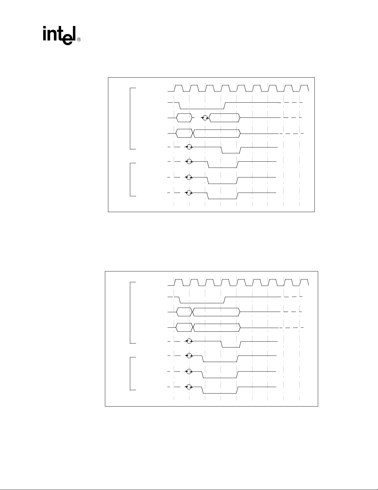
The figures below show CSR zero wait-state I/O read and write cycles. In the case of accessing the
Control/Status Registers, the CPU is the initiator and the 82559ER is the target of the transaction.
SYSTEM
CLK
FRAME#
AD
C/BE#
IRDY#
TRDY#
DEVSEL#
ADDR
I/O RD BE#
3421 56789
DATA
82559ER
STOP#
Fi
ure 2. CSR I/O Read Cycle
Read Accesses:
The CPU, as the initiator, drives address lines AD[31:0], the command and byte
enable lines C/BE#[3:0] and the control lines IRDY# and FRAME#. As a slave, the 82559ER
controls the TRDY# signal and provides valid data on each data access. The 82559ER allows the
CPU to issue only one read cycle when it accesses the Control/Status Registers, generating a
disconnect by asserting the STOP# signal. The CPU can insert wait states by de-asserting IRDY#
when it is not ready.
SYSTEM
CLK
FRAME#
AD
C/BE#
IRDY#
TRDY#
DEVSEL#
ADDR DATA
I/O WR BE#
3421 56789
82559ER
STOP#
Fi
ure 3. CSR I/O Write Cycle
Write Accesses:
The CPU, as the initiator, drives the address lines AD[31:0], the command and
byte enable lines C/BE#[3:0] and the control lines IRDY# and FRAME#. It also provides the
82559ER with valid data on each data access immediately after asserting IRDY#. The 82559ER
Datasheet
15
Page 22
GD82559ER — Networking Silicon
g
controls the TRDY# signal and asserts it from the data access. The 82559ER allows the CPU to
issue only one I/O write cycle to the Control/Status Registers, generating a disconnect by asserting
the STOP# signal. This is true for both memory mapped and I/O mapped accesses.
4.2.1.1.2 Flash Buffer Accesses
The CPU accesses to the Flash buffer are very slow. For this reason the 82559ER issues a targetdisconnect at the first data access. The 82559ER asserts the STOP# signal to indicate a targetdisconnect. The figures below illustrate memory CPU read and write accesses to the 128 Kbyte
Flash buffer. The longest burst cycle to the Flash buffer contains one data access only.
CLK
FRAME#
SYSTEM
AD
C/BE#
IRDY#
TRDY#
DEVSEL#
ADDR DATA
MEM RD BE#
82559ER
STOP#
ure 4. Flash Buffer Read Cycle
Fi
Read Accesses:
The CPU, as the initiator, drives the address lines AD[31:0], the command and
byte enable lines C/BE#[3:0] and the control lines IRDY# and FRAME#. The 82559ER controls
the TRDY# signal and de-asserts it for a certain number of clocks until valid data can be read from
the Flash buffer. When TRDY# is asserted, the 82559ER drives valid data on the AD[31:0] lines.
The CPU can also insert wait states by de-asserting IRDY# until it is ready. Flash buffer read
accesses can be byte or word length.
16
Datasheet
Page 23
g
g
CLK
FRAME#
Networkin
Silicon — GD82559ER
SYSTEM
AD
C/BE#
IRDY#
TRDY#
DEVSEL#
ADDR
MEM WR BE#
DATA
82559ER
STOP#
Fi
ure 5. Flash Buffer Write Cycle
Write Accesses:
byte enable lines
The CPU, as the initiator, drives the address lines
C/BE#[3:0] and
the control lines
IRDY#
82559ER with valid data immediately after asserting
and
IRDY#
FRAME#
AD[31:0],
. It also provides the
the command and
. The 82559ER controls the
TRDY#
signal and de-asserts it for a certain number of clocks until valid data is written to the Flash buffer.
By asserting
TRDY#
, the 82559ER signals the CPU that the current data access has completed.
Flash buffer write accesses can be byte length only.
4.2.1.1.3 Retry Premature Accesses
The 82559ER responds with a Retry to any configuration cycle accessing the 82559ER before the
completion of the automatic read of the EEPROM. The 82559ER m a y continue to Retry any
configuration accesses until the EEPROM read is complete. The 82559ER does not enforce the
rule that the retried master must attempt to access the same address again to complete any delayed
transaction. Any master access to the 82559ER after the completion of the EEPROM read will be
honored. Figure 6 depicts the operation of a Retry cycle.
Datasheet
17
Page 24
GD82559ER — Networking Silicon
g
g
SYSTEM
82559ER
CLK
FRAME#
IRDY#
TRDY#
DEVSEL#
STOP#
ure 6. PCI Retry Cycle
Fi
Note:
The 82559ER is considered the target in the above diagram; thus, TRDY# is not asserted.
4.2.1.1.4 Error Handlin
Data Parity Errors:
transaction. If an error was detected, the 82559ER always sets the Detected Parity Error bit in the
PCI Configuration Status register, bit 15. The 82559ER also asserts PERR#, if the Parity Error
Response bit is set (PCI Co nfigu ration Com mand regis ter, bit 6). The 82559ER does not attempt to
terminate a cycle in which a parity error was detected. This gives the initiator the option of
recovery.
Target-Disconnect:
•
After accesses to the Flash buffer
•
After accesses to its CSR
•
After accesses to the configuration space
System Error:
the SERR# Enable bit in the PCI Configuration Command register or the Parity Error Response bit
are not set, the 82559ER only sets the Detected Parity Error bit (PCI Configuration Status register,
bit 15). If SERR# Enable and Parity Error Response bits are both set, the 82559ER sets the
Signaled System Error bit (PCI Configuration Status register, bit 14) as well as the Detected Parity
Error bit and asserts SERR# fo r one clock.
The 82559ER, when detecting system error, will claim the cycle if it was the target of the
transaction and continue the transaction as if the address was correct.
The 82559ER checks for data parity errors while it is the target of the
The 82559ER prematurely terminate a cycle in the following cases:
The 82559ER reports pari ty error duri ng t he address phase usi ng th e SERR # pin. If
Note:
The 82559ER will report a system error for any parity error during an address phase, whether or
not it is involved in the current transaction.
4.2.1.2 82559ER Bus Master Operation
As a PCI Bus Master, the 82559ER initiates memory cycles to fetch data for transmission or
deposit received data and for accessing the memory resident control structures. The 82559ER
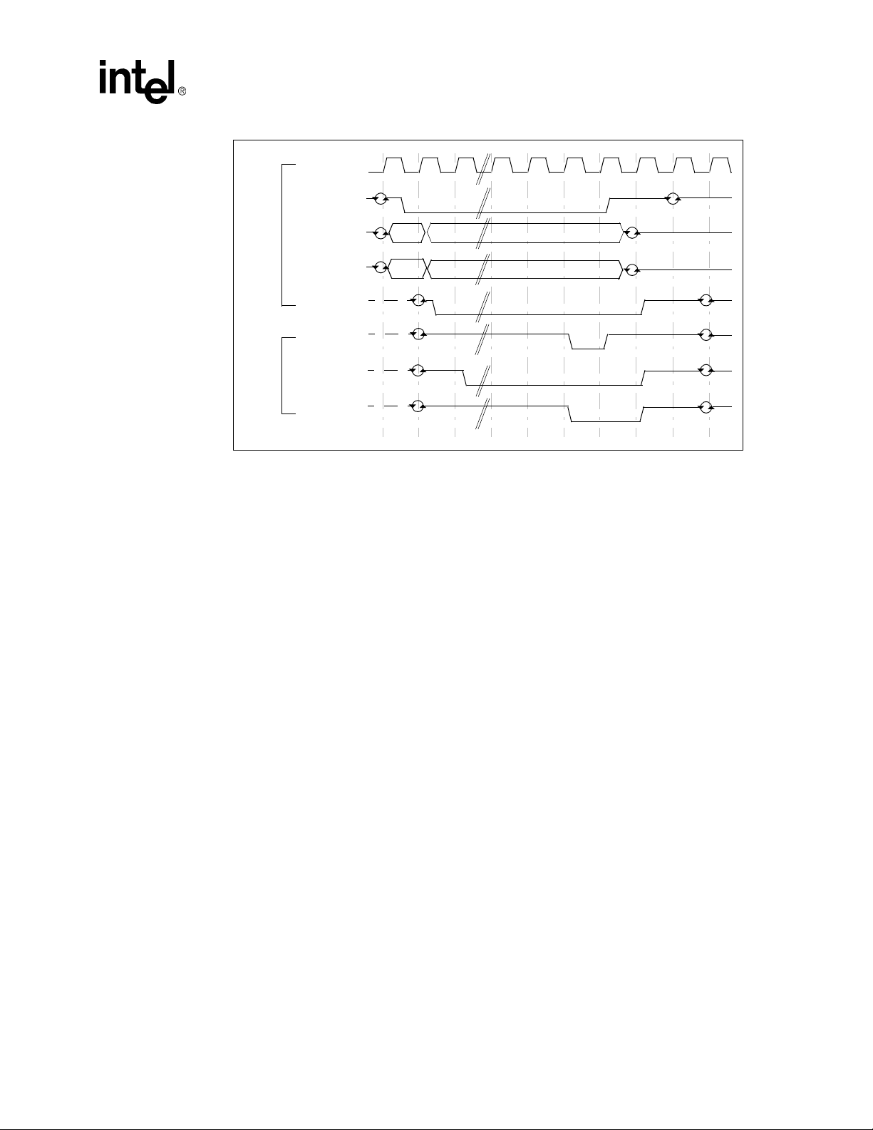
performs zero wait state burst read and write cycles to the host main memory. Figure 7 and Figure
18
Datasheet
Page 25
Networkin
g
g
g
Silicon — GD82559ER
8 depict memory read and write burst cycles. For bus master cycles, the 82559ER is the initiator
and the host main memory (or the PCI host bridge, depending on the configuration of the system) is
the target.
82559ERSYSTEM
82559ERSYSTEM
CLK
FRAME#
AD
C/BE#
IRDY#
TRDY#
DEVSEL#
CLK
FRAME#
AD
3421 5678910
ADDR
MR BE# BE#
ADDR
DATA
DATA
DATA
DATA
Fi
ure 7. Memory Read Burst Cycle
3421 5678910
DATA
DATA
DATA
DATA
DATA
DATA
C/BE#
MW BE# BE#
IRDY#
TRDY#
DEVSEL#
Fi
ure 8. Memory Write Burst Cycle
The CPU provides the 82559ER with action commands and pointers to the data buffers that reside
in host main memory. The 82559ER independently manages these structures and initiates burst
memory cycles to transfer data to and from them. The 82559ER uses the Memory Read Multiple
(MR Multiple) command for burst accesses to data buffers and the Memory Read Line (MR Line)
command for burst accesses to control structures. For all write accesses to the control structure, the
82559ER uses the Memory Write (MW) command. For write accesses to data structure, the
82559ER may use either the Memory Write or Memory Write and Invalidate (MWI) commands.
Read Accesses:
The 82559ER performs block transfers from host system memory to perform
frame transmission on the serial link. In this case, the 82559ER initiates zero wait state memory
read burst cycles for these accesses. The length of a burst is bounded by the system and the
82559ER’s internal FIFO. The length of a read burst may also be bounded by the value of the
Transmit DMA Maximum Byte Count in the Configure command. The Transmit DMA Maximum
Datasheet
19
Page 26

GD82559ER — Networking Silicon
Byte Count value indicates the maximum number of transmit DMA PCI cycles that will be
completed after an 82559ER internal arbitration. (Details on the Configure command are described
Software Developer’s Manual
in the
The 82559ER, as the initiator, drives the address lines AD[31:0], the command and byte enable
lines C/BE#[3:0] and the control lines IRDY# and FRAME#. The 82559ER asserts IRDY# to
support zero wait state burst cycles. The target signals the 82559ER that valid data is ready to be
read by asserting the TRDY# signal.
.)
Write Accesses:
reception. In this case, the 82559ER in itiates memory write burst cycles to deposit the data, usually
without wait states. The length of a burst is bounded by the system and the 82559ER’s internal
FIFO threshold. The length of a write burst m ay also be bo unded by the value of th e Receive DMA
Maximum Byte Count in the Configure command. The Receive DMA Maximum Byte Count value
indicates the maximum number of receive DMA PCI transfers that will be completed before the
82559ER internal arbitration. (Details on the Configure command are described in the
Developer’s Manual
The 82559ER, as the initiator, drives the address lines AD[31:0], the command and byte enable
lines C/BE#[3:0] and the control lines IRDY# and FRAME#. The 82559ER asserts IRDY# to
support zero wait state burst cycles. The 82559ER also drives valid data on AD[31:0] lines during
each data phase (from the first clock and on ). The target controls the length and signals completion
of a data phase by de-assertion and assertion of TRDY#.
Cycle Completion:
following cases:
Normal Complet i on
•
(for example, host main memory).
Backoff
•
82559ER by the arbiter, indicating that the 82559ER has been preempted by another bus
master.
Transmit or Receive DMA Maximum Byte Count
•
length specified in the Transmit or Receive DMA Maximum Byte Count field in the Configure
command block. (Details relating to this field and the Configure command are described in the
Software Dev eloper’s Manual
Target Termination
•
disconnect, target-retry, or target-abort. In the first two cases, the 82559ER initiates the cycle
again. In the case of a target-abort, the 82559ER sets the Received Target-Abort bit in the PCI
Configuration Status field (PCI Configuration Status register, bit 12) and does not re-initiate
the cycle.
Master Abort
•
82559ER (in other words, DEVSEL# has not been asserted). The 82559ER simply de-asserts
FRAME# and IRDY# as in the case of normal completion.
Error Condition
•
completes its current initiated transaction. Any further action taken by the 82559ER depends
on the type of error and other conditions.
The 82559ER performs block transfers to host system memory during frame
Software
.)
The 82559ER completes (terminates) its initiated memory burst cycles in the
: All transaction data has been transferred to or from the target device
: Latency Timer has expi red and the bus grant signal (GNT#) was removed from the
: The 82559ER burst has reached the
.)
: The target may request to terminate the transaction with a target-
: The target of the transaction has not responded to the address initiated by the
: In the event of parity or any other system error detection, the 82559ER
20
4.2.1.2.1 Memory Write and Invalidate
The 82559ER has four Direct Memory Access (DMA) channels. Of these four channels, the
Receive DMA is used to deposit the large number of data bytes received from the link into system
memory. The Receive DMA uses both the Memory Write (MW) and the Memory Write and
Invalidate (MWI) commands. To use MWI, the 82559ER must guarantee the following:
Datasheet
Page 27

Networkin
g
1. Minimum transfer of one cache line
2. Active byte enable bits (or BE#[3:0] are all low) during MWI access
3. The 82559ER may cross the cache line boundary only if it intends to transfer the next cache
line too.
To ensure the above conditions, the 82559ER may use the MWI command only if the following
conditions hold:
1. The Cache Line Size (CLS) written in the CLS register during PCI configuration is 8 or 16
Dwords.
2. The accessed address is cache line aligned.
3. The 82559ER has at least 8 or 16 Dwords of data in its receive FIFO.
4. There are at least 8 or 16 Dwords of data space left in the system memory buffer.
5. The MWI Enable bit in the PCI Configuration Co mman d register, bit 4, should is set to 1b.
6. The MWI Enable bit in the 82559ER Config ure command should is set to 1b. (Details on the
Configure command are described in the
If any one of the above conditions does not hold, the 8 2559ER will use the MW command. If a
MWI cycle has started and one of the conditions is no longer valid (for example, the data space in
the memory buffer is now less than CLS), then the 82559ER terminates the MWI cycle at the end
of the cache line. The next cycle will be either a MW or MWI cycle depending on the conditions
listed above.
Software Developer’s Manual
Silicon — GD82559ER
.)
If the 82559ER started a MW cycle and reached a cache line boundary, it either continues or
terminates the cycle depending on the Terminate Write on Cache Line configuration bit of the
82559ER Configure command (byte 3, bit 3). If this bit is set, the 82559ER terminates the MW
cycle and attempts to start a new cycle. The new cycle is a MWI cycle if this bit is set and all of the
above listed conditions are met. If the bit is not set, the 82559ER continues the MW cycle across
the cache line boundary if required. (Details on the Configure command are described in the
Software Developer’s Manual
.)
4.2.1.2.2 Read Align
The Read Align feature enhances the 82559ER’s performance in cache line oriented systems. In
these particular systems, starting a PCI transaction on a non-cache line aligned address may cause
low performance.
T o resolve this performance anomaly, the 82559ER attempts to terminate transmit DMA cycles on
a cache line boundary and start the next transaction on a cache line aligned address. This feature is
enabled when the Read Align Enable bit is set in the 82559ER Configure command (by te 3 , bit 2).
(Details on the Configure command are described in the
If this bit is set, the 82559ER operates as follows:
•
When the 82559ER is almost out of resources on the transmit DMA (that is, the transmit FIFO
is almost full), it attempts to terminate the read transaction on the nearest cache line boundary
when possible.
•
When the arbitration counter’s feature is enabled (in other words, the Transmit DMA
Maximum Byte Count value is set in the Configure command), the 82559ER switches to other
pending DMAs on the cache line boundary only.
Software Developer’s Manual
.)
Datasheet
Note the following:
21
Page 28

GD82559ER — Networking Silicon
g
•
This feature is not recommended for use in non-cache line oriented systems since it may cause
shorter bursts and lower performance.
•
This feature should be used only when the CLS register in PCI Configuration space is set to 8
or 16 Dwords.
•
The 82559ER reads all control data structures (including Receive Buffer Descriptors) fr om the
first Dword (even if it is not required) to maintain cache line alignment.
4.2.1.2.3 Error Handlin
Data Parity Errors:
during a transaction. If the Parity Error Response bit is set (P CI Configuration Command register,
bit 6), the 82559ER also asserts PERR# and sets the D a ta Parity Detected bit (PCI Configuration
Status register, bit 8). In addition, if the error was detected by the 82559ER during read cycles, it
sets the Detected Parity Error bit (PCI Configuration Status register, bit 15).
4.2.2 Clockrun Signal
The CLKRUN# signal is used to control the PCI clock as defined in the PCI Mobile design guide
and is compliant with the PCI Mobile design guide. The Clockrun signal is an open drain I/O
signal. It is used as a bidirectional channel between the host and the devices.
•
The host de-asserts the CLKRUN# signal to indicate that the PCI clock is about to be stopped
or slowed down to a non-operational frequency.
•
The host asserts the CLKRUN# signal when the interface clock is either running at a normal
operating frequency or about to be started.
•
The 82559ER asserts the CLKRUN# signal to indicate that it needs the PCI clock to prevent
the host from stopping the PCI clock or to request that the host restore the clock if it was
previously stopped.
Proper operation requires that the system latency from the nominal PCI CLK to CLKRUN#
assertion should be less than 0.5 µs. If the system latency is longer than 0.5 µs, the occurrence of
receive overruns increases. For use in these types of systems, the Clockrun functionality should be
disabled (see Section 8.1.12, “General Control Register” on page 61). In this case, the 82559ER
will claim the PCI clock even during idle time. If the CLKRUN# signal is not used , it sh ould be
connected to a pull-down resistor (62KΩ). The value of the resistor selected is dependent on the
ND-TREE set-up used (i.e. the test fixture must be able to overdrive pull-down).
As an initiator, the 82559ER checks and detects data parity errors that occur
4.2.3 Power Management Event Signal
The 82559ER supports power management indications in the PCI mode. The PME# output pin
provides an indication of a power management event to the system. PCI Power Management
In addition to the base functionality of the 82558 B-step, the 82559 family supports a larger set of
wake-up packets and the capability to wake th e sy stem on a link status change from a low power
state. The 82559ER enables the host system to be in a sleep state and remain virtually connected to
the network. After a power management event or link status change is detected, the 82559ER will
wake the host system. The sections below describe these events, the 82559ER power states, and
estimated power consumption at each power state.
22
Datasheet
Page 29

g
4.2.4 Pow er States
The 82559ER’s power management register implements all four power states as defined in the
Power Management Network Device Class Reference Specification, Revision 1.0. The four states,
D0 through D3, vary from maximum power consumption at D0 to the minimum power
consumption at D3. PCI transactions are only allowed in the D0 state, except for host accesses to
the 82559ER’s PCI configuration registers. The D1 and D2 power management states enable
intermediate power savings while providing the system wake-up capabilities. In the D3
the 82559ER can provide wake-up capabilities only if auxiliary power is supplied. Wake-up
indications from the 82559ER are provided by the Power Management Event (PME#).
4.2.4.1 D0 Power State
As defined in the Network Device Class Reference Specification , the dev ice is fully functional in
the D0 power state. In this state, the 82559ER receives full power and should be providing full
functionality. In the 82559ER the D0 state is partitioned into two substates, D0 Uninitialized (D0u)
and D0 Active (D0a).
D0u is the 82559ER’s initial power state following a PCI RST#. While in the D0u state, the
82559ER has PCI slave functionality to support its initialization by the host and supports wake up
events. Initialization of the CSR, Memory, or I/O Base Address Registers in the PCI Configuration
space switches the 82559ER from the D0u state to the D0a state.
Networkin
Silicon — GD82559ER
state,
cold
In the D0a state, the 82559ER provides its full functionality and consumes its nominal power. In
addition, the 82559ER supports wake on link status change (see Section 4.2.5, “Wake-up Events”
on page 27). While it is activ e, the 825 59E R requires a nominal P CI cloc k signal (in oth er word s, a
clock frequency greater than 16 MHz) for proper operation. During idle time, the 82559ER
supports a PCI clock signal suspension using the Clockrun signal mechanism. The 82559ER
supports a dynamic standby mode. In this mode, the 82559ER is able to save almost as much
power as it does in the static power-down states. The trans ition to or from standby is done
dynamically by the 82559ER and is transparent to the software.
4.2.4.2 D1 Power State
In order for a device to meet the D1 power state requirements, as specified in the Advanced
Configuration and Power Interface (ACPI) Specification, Revision 1.0, it must not allow bus
transmission or interrupts; however, bus reception is allowed. Therefore, device context may be
lost and the 82559ER does not initiate any PCI activity. In this state, the 82559ER responds only to
PCI accesses to its configuration space and system wake-up events.
The 82559ER retains link integrity and monitors the link for any wake-up events such as wake-up
packets or link status change. Following a wake-up ev ent, the 82559ER asserts the PME# signal to
alert the PCI based system.
4.2.4.3 D2 Power State
The ACPI D2 power state is similar in functionality to the D1 power state. If the bu s is in the B2
state, the 82559ER will consume less current than it does in the D1 state. In addition to D1
functionality, the 82559ER can provide a lower power mode with wake-on-link status change
capability. The 82559ER may enter this mode if the link is down while the 82559ER is in the D2
state. In this state, the 82559ER monitors the link fo r a transitio n from an invalid link to a valid
link. The 82559ER will not attempt to keep the link alive by transmitting idle symbols or link
integrity pulses.
configuration bit in the Power Management Driver Register (PMDR).
1
The sub-10 mA state due to an invalid link can be enabled or disabled by a
Datasheet
23
Page 30

GD82559ER — Networking Silicon
4.2.4.4 D3 Power State
In the D3 power state, the 82559ER has the same capabilities and consumes the same amount of
power as it does in the D2 state. However, it enables the PCI system to be in the B3 state. If the PCI
system is in the B3 state (in other words , no PCI power is present ), the 825 59ER pro vides wake-up
capabilities if it is connected to an auxiliary power source in the system. If PME is disabled, the
82559ER does not provide wake-up capability or maintain link integrity. In this mode the 82559ER
consumes its minimal power.
The 82559ER enables a system to be in a sub-5 watt state (low power state) and still be virtually
connected. More specifically, the 82559ER supports full wake-up capabilities while it is in the
D3
state. The 82559ER can be connected to an auxiliary power source (V
cold
to provide wake-up functionality while the PCI power is off. The typical current consumption of
the 82559ER is 125 mA at 3.3 V. Thus, a dual power plane is not required. If connected to an
auxiliary power source, the 82559ER receives all of its power from the auxiliary source in all
power states.
4.2.4.5 Understanding Power Requirements
When running the 82559ER off a 3.3V_standby power source, the actual power consumption will
scale with network traffic. In other words, if the 82559ER is monitoring the network for ACPI
“Interesting Packets” only the PCI bus specific circuitry will be disabled. As an a example the
8259ER will typically draw approximately 120mA, in D1-D3 under a full Ethernet load. In the D0
state, the 82559ER will typically consume 125mA under the same load conditions.
), which enables it
AUX
The tables below summarizes the 82559ER’s functionality and power consumption at the different
power states
Power State Conditions 100 Mbs 10 Mbs
D0 Maximum 175 mA 140 mA
D0 Average (5 Mbs) 125 mA 115 mA
D0
D2/D3 (link
down)
Dx (x>0 with
PME# disabled)
NOTE:
All values shown for the D3 state assume the availability of 3.3 V Standby available to the
Dynamic standby
(With Network Load)
PCI CLK 10 mA 10 mA
w/o PCI CLK 3 mA 3 mA
PCI CLK 10 mA 10 mA
w/o PCI CLK 3 mA 3 mA
120 mA 55 mA
device.
1. For a topology of two 82559E R de vices connected by a crossed twisted-pa ir Ethernet cable, the deep power -down mode should be
disabled. If it is enabled, the two devices may not detect each other if the operating system places them into a low power state before both
nodes become active.
24
Datasheet
Page 31

Networkin
g
y
y
g
g
g
y
)
y
)
)
y
)
y
Silicon — GD82559ER
.
Power State Link 82559ER Functionality
D0u Don’t care
D0a
D1
D2
D3 (with power
Dx (x>0 without
PME#
Valid
Invalid Full functionalit
Valid
Invalid
Valid Same functionalit
Invalid Detection for valid link and no link integrit
Valid Same functionality as D1 (link valid
Invalid Detection for valid link and no link integrit
Don’t Care No wake-up functionalit
• Power-up state
• PCI slave access
Full functionalit
link
• Wake-up on “interestin
invalid
• PCI confi
• Wake on link valid
• PCI confi
at full power and wake on invalid
at full power and wake on valid link
uration access
uration access
as D1 (link valid
” packets and link
4.2.4.6 Auxiliary Power Signal
The 82559ER senses whether it is connected to the PCI power supply or to an auxiliary power
supply (V
) via the FLA1/AUXPWR pin. The auxiliary power detection pin (multiplexed with
AUX
FLA1) is sampled when the PCI RST# or ALTRST# signals are active. An external pull-up resistor
should be connected to the 82559ER if it is fed by V
should be left floating. The presence of AUXPWR affects the value reported in the Power
Management Capability Register (PCI Configuration Space, offset DEH). The Power Management
Capability Register is described in more detail in Section 7.1.18, “Power Management Capabilities
Register” on page 54.
4.2.4.7 Alternate Reset Signal
The 82559ER’s ALTRST# input pin functions as a power-on reset input. Following ALTRST#
being driven low, the 82559ER is initialized to a known state. In systems that support auxili ary
power, this pin should be connected to the auxiliary power’s power stable signal (power good) of
the 82559ER’s power source. In a LAN on Motherboard solution, this signal is available on the
system. In network adapter implementations, an external analog device connected to the auxiliary
power supply can be used to produce this signal. In systems that do not have an auxiliary power
source, the ALTRST# signal should be tied to a pull-up resistor.
4.2.4.7.1 Isolate Signal
When the 82559ER is connected to V
In this case, the 82559ER isolates itself from the PCI bus. The 82559ER has a dedicated
ISOLATE# pin that should be connected to the PCI power source’s stable power signal (power
good). Whenever the PCI Bus is in the B3 state, the PCI power good signal becomes inactive and
the 82559ER isolates itself from the PCI bus. During this state, the 82559ER ignores all PCI
signals including the RST# and CLK signals. It also tri-states all PCI outputs, except the PME#
signal. In the transition to an active PCI power state (in other words, from B3 power state to B0
power state), the PCI power good signal shifts high.
; otherwise, the FLA1/AUXPWR pin
AUX
, it may be powered on whi l e the PCI bus is powered off.
AUX
Datasheet
25
Page 32

GD82559ER — Networking Silicon
g
In a LAN on Motherboard solution, the PCI power good signal is supplied by the system. In
network adapter implementations, the PCI power go od sign al can b e eith er g enerated locally using
an external analog device, or connected directly to the PCI reset signal. In designs, that use both the
ISOLATE# and RST# pins of the 82559ER, the PCI power good signal should envelope
ISOLATE#, as shown below. For designs that use the PCI reset signal, the RST# pin on the
82559ER should be tied to the PCI power rail (through a 4.7
be connected to the 82559ER’s ISOLATE# pin.
PCI power good signal
Required ISOLATE#
signal behavior
In many systems, the PCI RST# signal is asserted low whenever the PCI bus is inactive. In these
systems, the 82559ER B-step device and later devices allow the ISOLATE# pin to be driven from
the PCI RST# signal. In this case, the ALTRST# pin on the 82559ER should be pulled high to the
PCI bus high voltage level.
ΚΩ)
, and the PCI reset signal should
ure 9. Isolate Signal Behavior to PCI Power Good Signal
Fi
Note:
4.2.4.7.2 PCI Reset Signal
The PCI RST# signal may be activated in one of the following cases:
•
Power-up
•
Warm boot
•
Wake-up (B3 to B0 transition)
•
Set to power-down (B0 to B3 transi tion)
If PME is enabled (in the PCI power management registers), the RST# signal does not affect any
PME related circuits (in other words, PCI power management registers, and the wake-up packet
would not be affected). While the RST# signal is active, the 82559ER ignores other PCI signals
and floats its outputs. However, if AUXPWR is asserted, the RST# signal has no affect on any
circuitry.
While the 82559ER is in the D0, D1, or D2 power state, it is initialized by the RST# level. When
the 82559ER is in the D3 power state, the system bus may be in the B3 bus power state. In the B3
power state, the PCI RST# signal is undefined; however, the auxiliary power source proposal for
the PCI Specification, Revision 2.2 is for the PCI RST# signal to be an active low. Therefore, the
82559ER uses the PCI RST# similarly to the ISOLATE# signal in D3 power state. Following the
trailing edge of the PCI RST#, the 82559ER is initialized while preserving the PME# signal and its
context.
According to the PCI specification, during the B3 state, the RST# signal is undefined.
The transition from the B3 power state to the B0 power state occurs o n the trailing edge of the
RST# signal.
The initialization signal is generated internally in th e following cases:
•
Active RST# signal while the 82559ER is the D0, D1, or D2 power state
•
RST# trailing edge while the 82559ER is in the D3 power state
26
Datasheet
Page 33

Networkin
g
g
•
ISOLATE# trailing edge
The internal initialization signal resets the PCI Configuration Space, MAC configuration, and
memory structure.
The behavior of the PCI RST# signal and the internal 82559ER initialization signal are shown in
the figure below.
D0 - D2 power state
PCI RST#
Internal hardware
reset
D3 power state
PCI RST#
Silicon — GD82559ER
Internal hardware
reset
ISOLATE#
Internal hardware
reset
ure 10. 82559ER Initialization upon PCI RST# and ISOLATE#
Fi
4.2.5 Wake- up Events
There are two types of wake-up events: “Interesting” Packets and Link Status Change. These two
events are detailed below.
Note:
4.2.5.1 “Interesting” Packet Events
The wake-up event is supported only if the PME Enable bit in the Power Management Control/
Status (PMCSR) register is set. (The PMCSR is described in Section 7.1.19, “Power Management
Control/Status Register (PMCSR)” on page 55.)
In the power-down state, the 82559ER is capable of recognizing “interesting” packets. The
82559ER supports pre-defined and programmable packets that can be defined as any of the
following:
•
ARP Packets (with Multiple IP addresses)
•
Direct Packets (with or without type qualification)
•
Neighbor Discovery Multicast Address Packet (‘ARP’ in IPv6 environment)
•
NetBIOS over TCP/IP (NBT) Query Packet (under IPv4)
•
Internetwork Package Exchange* (IPX) Diagnostic Packet
640 ns
Internal reset
due to ISOLATE#
640 ns
This allows the 82559ER to handle various packet types. In general, the 82559ER supports
programmable filtering of any packet in the first 128 bytes.
Datasheet
27
Page 34

GD82559ER — Networking Silicon
4.2.5.2 Link Status Change Event
The 82559ER link status indication circuit is capable of issuing a PME on a link status change from
a valid link to an invalid link conditi on or vice versa . The 82559ER rep orts a PME link statu s event
in all power states. The PME# signal is gated by the PME Enable bit in the PMC SR and the CSMA
Configure command, which is described in the Software Developer’s Manual.
4.3 Parallel Flash Interface
The 82559ER’s parallel interface is used primarily as a Flash interface. The 82559ER supports a
glueless interface to an 8-bit wide, 128 Kbyte, parallel memory device.
The Flash (or boot PROM) is read from or written to whenever the host CPU performs a read or a
write operation to a memory location that is within the Flash mapping window. All accesses to the
Flash, except read accesses, require the appropriate command sequence for the device used. (Refer
to the specific Flash data sheet for mo re details on reading f rom or writi ng to the Fl ash device.) Th e
accesses to the Flash are based on a direct decode of CPU accesses to a memory window defined in
either the 82559ER Flash Base Address Register (PCI Configuration space at offset 18H) or the
Expansion ROM Base Address Register (PCI Configuration space at offset 30H). The 82559ER
asserts control to the Flash when it decodes a valid access.
The 82559ER supports an external Flash memory (or boot PROM) of up to 128 Kbyte. The
Expansion ROM BAR can be separately disabled by setting the corresponding bit in the EEPROM,
word AH.
Note:
Flash accesses must always be assembled or disassembled by the 82559ER whenever the access is
greater than a byte-wide access. Due to slow access times to a typical Flash and to avoid violating
PCI bus holding specifications (no more than 16 wait states inserted for any cycles that are not
system initiation cycles), the maximum data size is either one word or one byte for a read operation
and one byte only for a write operation.
4.4 Serial EEPROM Interface
The serial EEPROM stores configuration data for the 82559ER and is a serial in/serial out device.
The 82559ER supports a either a 64 register or 256 register size EEPROM and automatically
detects the EEPROM’s size. The EEPROM should operate at a frequency of at least 1 MHz.
28
Datasheet
Page 35

Networkin
g
g
y
y
y
y
Silicon — GD82559ER
All accesses, either read or write, are preceded by a command instruction to the device. The
address field is six bits for a 64 register EEPROM or eight bits for a 256 register EEPROM. The
end of the address field is indicated by a dummy zero bit from the EEPROM, which indicates the
entire address field has been transferred to the device. An EEPROM read instruction waveform is
shown in the figure below.
EESK
EECS
A1A
A
A1A
0
2
0
D
15
D
0
EEDI
EEDO
A5A
READ OP code
Fi
ure 11. 64 Word EEPROM Read Instruction Waveform
A
4
3
The 82559ER performs an auto matic read of seven wor ds (0H, 1H, 2H, AH, Bh , Ch and DH) of the
EEPROM after the de-assertion of Reset.
The 82559ER EEPROM format is shown below in Figure 12.
Word1514131211109876543210
0H IA B
1H IA B
2H IA B
AH
Sig ID 0b BD Rev ID 1b DPD 0b 00b 0b STB
te 2 IA Byte 1
te 4 IA Byte 3
te 6 IA Byte 5
Ena
0b
BH Subsystem ID
CH Subs
stem Vendor ID
DH Reserved
Figure 12. 82559ER EEPROM Format
Datasheet
29
Page 36

GD82559ER — Networking Silicon
p
g
g
g
g
g
q
y
g
q
q
y
q
y
q
q
y
g
q
Note that word 0Ah contains several configuration bits. Bits from word 0Ah, FBh through FEh,
and certain bits from word 0Dh are described as follows:
Table 1. EEPROM Words Field Descri
Word Bits Name Description
Word A
D
FBh -
FEh
5:14 Signature The Signature field is a signature of 01b, indicating to the 82559ER that there is
13 Reserved Reserved Default value is 0b.
12 Reserved This bit is reserved and should be set to 0b.
11 Boot Disable The Boot Disable bit disables the Expansion ROM Base Address Re
10:8 Revision ID These three bits are used as the three least si
7 Reserved Reserved and should be set to 0b
6 Deep Power
5 Reserved Reserved and should be set to 0b.
4:3 Reserved These are reserved and should be set to 00b.
2
1 Standb
0 Reserved Set this bit e
11:8 Reserved Reserved.
7:0 Reserved
ALL Reserved
Down
Enable The Standby Enable bit enables the 82559ER to enter standby mode. When
a valid EEPROM present. If the Si
nored and the default values are used.
i
uration space, offset 30H) when it is set. Default value is 0b.
Confi
revision, if bits 15, 14, and 13 e
Section 7.1.10, “PCI Subs
e53. The default value depends on the silicon revision.
pa
This bit is used as the Deep Power Down enable/disable bit. When the DPD bit
e
uals 0b, deep power down is enabled in the D3 power state while PME is
disabled. If the DPD bit e
power state while PME is disabled.
this bit e
standb
The 82559ER does not re
e
remains in an active state. Thus, the 82559ER will alwa
usin
uals 1b, the 82559ER is able to recognize an idle state and can enter
mode (some internal clocks are stopped for power saving purposes).
uals 0b, the idle recognition circuit is disabled and the 82559ER always
the Clockrun mechanism.
ual to 0b for compatibility.
uals 1b, deep power down is disabled in the D3
nature field is not 01b, the other bits are
ual 011b and the ID was set as described in
stem Vendor ID and Subsystem ID Registers” on
uire a PCI clock signal in standby mode. If this bit
tions
ister (PCI
nificant bits of the device
s request PCI CLK
Note:
The IA read from the EEPROM is used by the 82559ER until an IA Setup command is issued by
software. The IA defined by the IA Setup command overrides the IA read from the EEPROM.
4.5 10/100 Mbps CSMA/CD Unit
The 82559ER CSMA/CD unit implements both the IEEE 802.3 Ethernet 10 Mbps and IEEE
802.3u Fast Ethernet 100 Mb ps standa rds. It perfo rms all the C SMA/CD proto col functi ons such as
transmission, reception, collision handling, etc. The 82559ER CSMA/CD unit interfaces the
internal PHY unit through a standard Media Independent Interface (MII), as specified by IEEE
802.3, Chapter 22. This is a 10/100 Mbps mode in which the data stream is nibble-wide and the
serial clocks run at either 25 or 2.5 MHz.
30
Datasheet
Page 37

g
4.5.1 Full Duplex
When operating in full duplex mode the 8 2559ER can tran smit and receive frames simultan eously.
Transmission starts regardless of the state of the internal receive path. Reception starts when the
internal PHY detects a valid frame on the receive differential pair of the PHY.
The 82559ER operates in either half duplex mode or full duplex mode. For proper operation, both
the 82559ER CSMA/CD module and the PHY unit must be set to the same duplex mode. The
CSMA duplex mode is set by the 82559ER Configure command or forced by automatically
tracking the mode in the PHY unit.
The PHY duplex mode is set either by Auto-Negotiation or, if Auto-Negotiation is disabled, by
setting the full duplex bit in the Management Data Interface (MDI) Register 0, bit 8. By default, the
internal PHY unit advertises full duplex ability in the Auto-Negotiation process regardless of the
duplex setting of the CSMA unit. The CSMA configuratio n should match the result of the AutoNegotiation.
The selection of duplex operation (full or half) and flow control is done in two levels: MAC and
PHY. The MAC duplex selection is done only through CSMA configuration mechanism (in other
words, the Configure command from software).
4.5.2 Flow Control
Networkin
Silicon — GD82559ER
The 82559ER supports IEEE 802.3x frame based flow control frames only in both full duplex and
half duplex switched environm ents. The 825 59ER flow con trol featur e is not intend ed to be used in
shared media environments.
Flow control is optional in full duplex mode and can be selected through software configuration.
There are three modes of flow control that can be selected: frame based transmit flow control,
frame based receive flow control, and none.
The PHY unit’s duplex and flow control enable can be selected using NWay* Auto-Negotiation
algorithm or through the Management Data Interface.
4.5.3 Address Filtering Modifications
The 82559ER can be configured to ignore one bit when checking for its Individual Address (IA) on
incoming receive frames. The address bit, known as the Upp er/Lower (U/L) bit, is the secon d least
significant bit of the first byte of the IA. This bit may be used, in some cases, as a priority
indication bit. When configured to do so, the 82559ER passes any frame that matches all other 47
address bits of its IA, regardless of the U/L bit value.
This configuration only affects the 82559ER specific IA and not multicast, multi-IA or broadcast
address filtering. The 82559ER does not attribute any p riority to frames with this bit set, it simply
passes them to memory regardless of this bit.
4.5.4 Long Frame Reception
Datasheet
The 82559ER supports the reception of long frames, specifically frames longer than 1518 bytes,
including the CRC, if software sets the Long Receive OK bit in the Configuration command
(described in the Software Developer’s Manual). Otherwise, “long” frames are discarded.
31
Page 38

GD82559ER — Networking Silicon
4.6 Media Independent Interface (MII) Management Interface
The MII management interface allows the CPU to control the PHY unit via a control register in the
82559ER. This allows the software driver to place the PHY in specific modes such as full duplex,
loopback, power down, etc., without the need for specific hard ware pins to sel ect the desired mod e.
This structure allows the 82559ER to query the PHY unit for status of the link. This register is the
MDI Control Register and resides at offset 10h in the 82559ER CSR. (The MDI registers are
described in detail in Section 9., “PHY Unit Registers” on page 65.) The CPU writes commands to
this register and the 82559 ER r eads or writes the co ntrol/ stat us par ameters to th e PHY unit throu gh
the MDI register. Although the 82559ER follows the MII format, the MI bus is not accessible on
external pins.
32
Datasheet
Page 39

Networkin
g
y
5. GD82559ER Test Port Functionalit
5.1 Introduction
The 82559ER’s NAND-Tree Test Access Port (TAP) is the access point for test data to and from
the device. The port provides the ability to perform basic production level testing. The port provides two functions:
1) The the synchronous IC validation mode used in the production of the device. This mode gives
the signals their names (i.e TCK, Testability Port Clock).
2) In addition to the synchronous test mode, the 82559ER supports asynchonous testing modes.
These test modes support the validation of connections at the board level.
5.2 Asynchronous Test Mode
Four asynchronous test modes are supported for system level design use. The modes are selected
through the use of Test Port input pin in static combinations. The Test Port pins are: TEST, TI,
TEXEC and TCK. During normal operation the Test pin must be pulled down through a resistor
(pulling Test high enables the test mode). All other Port inputs may have a pull-down at the designers discretion.
Silicon — GD82559ER
5.3 Test Function Description
The 82559 TAP mode supports several tests that can be used in board l evel des ign. Th ese t es ts can
help in the verification of basic functionality. As well as test the integrity of solder connection on
the board. The tests are as follows:
5.4 85/85
The 85/85 test provides the same functionality to the bo ard level designer as the Tristate mode.
This mode is normal used during chip the chip burn-in cycling. The 82559ER is placed in this
o
mode during the 85
TEXEC = ‘1, TI = ‘1
/85% humidity test cycling. Test Pin Combinations: TEST = ‘1, TCK = ‘0,
Datasheet
33
Page 40

GD82559ER — Networking Silicon
5.5 TriState
This command set all 82559ER Input and Output pins into a TRI-state (HIGH-Z) mode, all internal
pull-ups and pull-downs are disabled. This mode is entered by setting the following Test Pin Com-
binations: TEST = ‘1, TCK = ‘0, TEXEC = ‘0,
5.6 Nand - Tree
The NAND-Tree test mode is the most useful of the asynchronous test modes. The test enables the
placement of the 82559ER to be validated at board test. NAND-Tree was chosen for its speed
advantages. Modern automated test equipment can complete a complete peripheral scan without
support at the board level. This command connects all the outputs of the input-buffers in the device
periphery into a NAND - tree scheme. All the output drivers of the ou tput-buf fers except the T OUT
pin, are put into HIGH-Z mode. These pins can then be driven to affect the output of the tree. There
are two separate chains and associated outputs for speed. Any h a rd strap ped pins will prevent the
tester from scanning correctly. This mode is enter by placing the Test Pin in the following Combinations: TEST = ‘1, TCK = ‘0, TEXEC = ‘1, TI = ‘0
There are two nand-tree chains with two separate outputs assigned to FLOE# (Chain 1) and
FLWE# (Chain 2).
TI = ‘1, and resetting the device.
Table 2. Nand - Tree Chains
Chain Order Chain 1 Chain 2
1RST#LILED
2 IDSEL ACTLED#
3 REQ# SPEEDLED
4AD23ISOLATE#
5 SERR# ALTRST#
6 AD22 CLKRUN#
7 AD21 AD31
8 AD20 AD30
9 AD19 AD29
10 AD18 AD28
11 AD17 AD27
12 C/BE2# PME#
13 FRAME# AD26
14 IRDY# AD25
15 TRDY# C/BE3#
16 CLK AD24
17 DEVSEL# FLD0
18 INTA# FLD1
34
NAND-Tree Output FLOE# FLWE#
Datasheet
Page 41

Networkin
g
Silicon — GD82559ER
Table 2. Nand - Tre e Chains
Chain Order Chain 1 Chain 2
19 STOP# FLD2
20 GNT# FLD3
21 PERR# FLD4
22 PAR FLD5
23 AD16 FLD6
24 C/BE1# FLD7
25 AD15 FLA0
26 AD14 FLA1
27 AD13 FLA2
28 AD12 FLA3
29 AD11 FLA4
30 AD10 FLA5
31 AD9 FLA6
32 AD8 FLA7
33 C/BE0# FLA8
34 AD7 FLA9
35 AD6 FLA10
36 AD5 FLA11
37 AD4 FLA12
37 AD3 FLA13/EEDI
39 AD2 FLA14/EEDO
40 AD1 FLA15/EESK
41 AD0 FLA16
42 EECS FLCS#
43
44
45
46
Datasheet
NAND-Tree Output FLOE# FLWE#
35
Page 42

GD82559ER — Networking Silicon
36
Datasheet
Page 43

Networkin
g
Silicon — GD82559ER
6. GD82559ER Physical Layer Functional Description
6.1 100BASE-TX PHY Unit
6.1.1 100BASE-TX Transmit Clock Generation
A 25 MHz crystal or a 25 MHz oscillator is used to drive the PHY unit’s X1 and X2 pins. The PHY
unit derives its internal transmit digital clocks from thi s crystal or oscillator input. The internal
Transmit Clock signal is a derivative of the 25 MHz internal clock. The accuracy of the external
crystal or oscillator must be ± 0.0005% (50 PPM).
6.1.2 100BASE-TX Transmit Blocks
The transmit subsection of the PHY unit accepts nibble-wide data from the CSMA/CD unit. The
transmit subsection passes data unconditionally to the 4B/5B encoder.
The 4B/5B encoder accepts nibble-wide data (4 bits) from the CSMA unit and compi les it into 5bit-wide parallel symbols. These symbols are scrambled and serialized into a 12 5 Mb ps bit stream,
converted by the analog transmit driver into a MLT-3 waveform format, and transmitted onto the
Unshielded Twisted Pair (UTP) or Shielded Twis ted Pair (STP) wire.
6.1.2.1 100BASE-TX 4B/5B Encoder
The 4B/5B encoder complies with the IEEE 802.3u 100BASE-TX standard. Four bits are encoded
according to the transmit 4B/5B lookup table. The lookup table matches a 5-bit code to each 4-bit
code.
The table below illustrates the 4B/5B encoding scheme ass ociated with the given symbol.
Symbol 5B Symbol Code 4B Nibble Code
0 11110 0000
1 01001 0001
2 10100 0010
3 10101 0011
4 01010 0100
5 01011 0101
6 01110 0110
7 01111 0111
8 10010 1000
9 10011 1001
A 10110 1010
B 10111 1011
C 11010 1100
D 11011 1101
Table 3. 4B/5B Encoder
Datasheet
37
Page 44

GD82559ER — Networking Silicon
y
(
)
y
y
y
y
Symbol 5B Symbol Code 4B Nibble Code
E 11100 1110
K 10001
R 00111
V 00000 INVALID
V 00001 INVALID
V 00010 INVALID
V 00011 INVALID
H 00100 INVALID
V 00101 INVALID
V 00110 INVALID
V 01000 INVALID
V 01100 INVALID
V 10000 PHY based Flow Control
V 11001 INVALID
Table 3. 4B/5B Encoder
F 11101 1111
I 11111
J 11000
T 01101 1st End of Packet S
Inter Packet Idle S
No 4B
1st Start of Packet S
0101
2nd Start of Packet S
0101
2nd End of Packet S
and Flow Control
mbol
mbol
mbol
mbol
mbol
6.1.2.2 100BASE-TX Scrambler and MLT-3 Encoder
Data is scrambled in 100BASE- TX to redu ce electr omagnet ic emiss ions du ring long tran smis sions
of high-frequency data codes. The scramb ler logic accepts 5 bits fro m the 4B/5B encode r block and
presents the scrambled data to the MLT-3 encoder. The PHY unit implements the 11-bit stream
cipher scrambler as adopted by the ANSI XT3T9.5 committee for UTP operation. The cipher
equation used is:
X[n] = X[n-11] + X[n-9] (mod 2)
The encoder receives the scrambled Non-Return to Zero (NRZ) data stream from the Scrambler
and encodes the stream into MLT-3 for presentation to the driver. MLT-3 is similar to NRZI
coding, but three levels are output instead of two. There are three output levels: p ositive, negative
and zero. When an NRZ “0” arrives at the input of the encoder, the last output level is maintained
(either positive, negative or zero). When an NRZ “1” arrives at the input of the encoder, the output
steps to the next level. The order of steps is negative-zero-positive-zero which continues
periodically.
38
Datasheet
Page 45

g
g
g
Clock
g
(V
TDP-VTDN
)
+1V
0V
-1V
t
g
g
g
g
Networkin
Silicon — GD82559ER
NRZ
NRZ1
MLT-3
1100 0110
1100 0110
1100 0110
Fi
ure 13. NRZ to MLT-3 Encoding Diagram
6.1.2.3 100BASE-TX Transmit Framin
The PHY unit does not differentiate between the fields of the MAC frame containing preamble,
Start of Frame Delimiter, data and Cyclic Redundancy Check (CRC). The PHY unit encodes the
first byte of the preamble as the “JK” symbol, encodes all other pieces of data according to the 4B/
5B lookup table, and adds the “TR” code after the end of the packet. The PHY unit scrambles and
serializes the data into a 125 Mbps stream, encodes it as MLT-3, and drives it onto the wire.
6.1.2.4 Transmit Driver
The transmit differential pair lines are implemented with a digital slope controlled current driver
that meets the TP-PMD specifications. Current is sinked from the isolation transformer by the TDP
and TDN pins. The conceptual transmit differential waveform for 100 Mbps is illustrated in the
following figure.
ure 14. Conceptual Transmit Differential Waveform
Fi
The magnetics module that is external to the PHY unit converts I
TDP
and I
to the 2.0 Vpp, as
TDN
required by the TP-PMD specification. The same magnetics used for 100BASE-TX mode should
also work in 10BASE-T mode. The following is a list of current magnetics modules available from
several vendors:
Table 4. Magnetics Modules
Vendor Model/Type 100BASE-TX 10BASE-T
Delta LF8200A Yes Yes
Pulse En
Pulse En
Datasheet
ineerin
ineerin
PE-68515 Yes Yes
H1012 Yes Yes
39
Page 46

GD82559ER — Networking Silicon
y
g
g
6.1.3 100BASE-TX Receive Blocks
The receive subsection of the PHY unit accepts 100BASE-TX MLT-3 data on the receive
differential pair. Due to the advanced digital signal processing design techniques employed, the
PHY unit will accurately receive valid data from Category-5 (CAT5) UTP and Type 1 STP cable of
length well in excess of 100 meters.
6.1.3.1 Adaptive Equalizer
The distorted MLT-3 signal at the end of the wire is restored by the equalizer. The equalizer
performs adaptation based on the shape of the received signal, equalizing the signal to meet
superior Data Dependent Jitter performance.
6.1.3.2 Receive Clock and Data Recover
The clock recovery circuit uses advanced digital signal processing technology to compensate for
various signal jitter causes. The circuit recovers the 125 MHz clock and data and presents the data
to the MLT-3 decoder.
6.1.3.3 MLT-3 Decoder, Descrambler, and Receive Digital Section
The PHY unit first decodes the MLT-3 data; afterwards, the descrambler reproduces the 5B
symbols originated in the transmitter . The descrambling is based on synchronization to the transmit
11-bit Linear Feedback Shift Register (LFSR) during idle. The data is decoded at the 4B/5B
decoder. Once the 4B symbols are obtained, the PHY unit outputs the receive data to the CSMA
unit.
6.1.3.4 100BASE-TX Receive Framin
The PHY unit does not differentiate between the fields of the MAC frame containing preamble,
start of frame delimiter, data and CRC. During 100 Mbps reception, the PHY unit differentiates
between the idle condition ("L" symbols on the wire) and the preamble or start of frame delimiter.
When two non-consecutive bits are 0b within 10 bits (125 Mbps 5B data coding) the PHY unit
immediately asserts carrier sense. When the “JK” symbols (“11000, 10001”) are fully recognized,
the PHY unit provides the received data to the CSMA unit. If the “JK” symbol is not recognized
(“false carrier sense”), the carrier sense is immediately de-asserted and a receive error is indicated.
6.1.3.5 100BASE-TX Receive Error Detection and Reportin
In 100BASE-TX mode, the PHY unit can detect errors in receive data in a number o f ways. Any of
the following conditions is considered an error:
•
Link integrity fails in the middle of frame reception.
•
The Start of Stream Delimiter (SSD) “JK” symbol is not fully detected after idle.
•
An invalid symbol is detected at the 4B/5B decoder.
•
Idle is detected in the middle of a frame (before “TR” is detected).
When any of the above error conditions occurs, the PHY unit immediately asserts its receive error
indication to the CSMA unit. The receive error ind i cation is held active as long as the receive error
condition persists on the receive pair.
40
Datasheet
Page 47

Networkin
g
y
y
Silicon — GD82559ER
6.1.4 100BASE-TX Collision Detection
100BASE-TX collisions in half duplex mode onl y are detected similarly to 10BASE-T collision
detection, via simultaneous transmission and reception.
6.1.5 100BASE-TX Link Integrity and Auto-Negotiation Solution
The 82559 Auto-Negotiation function automatically configures the device to the technology,
media, and speed to operate with its link partner. Auto-Negotiation is widely described in IEEE
specification 802.3u, clause 28. The PHY unit supports 10BASE-T half duplex, 10BASE-T full
duplex, 100BASE-TX half duplex, and 100BASE-TX full duplex.
The PHY unit has two Physical Media Attachment (PMA) technologi es with its link integrity
function, 10BASE-T and 100BASE-TX.
6.1.5.1 Link Integrit
In 100BASE-TX, the link integrity function is determined by a stable signal status coming from the
TP-PMD block. Signal status is asserted when the PMD detects breaking squelch energy and the
right bit error rate according to the ANSI specification.
6.1.5.2 Auto-Negotiation
The PHY unit fully supports IEEE 802.3u, clause 28. The technology, 10BASE-T or 100BASETX, is determined by the Auto-Negotiation result.
Speed and duplex auto-select are functions of Auto-Negotiation. However, these parameters may
be manually configured via the MII management interface (MDI registers).
6.1.6 Auto 10/100 Mbps Speed Selection
The MAC may either allow the PHY unit to automatically select its operating speed or force the
PHY into 10 Mbps or 100 Mbps mode. The Management Data Interface (MDI) can control the
PHY unit speed mode.
The PHY unit auto-select function determines the operation speed of the media based on the link
integrity pulses it receives. If no Fast Link Pulses (FLPs) are detected and Normal Link Pulses
(NLPs) are detected, the PHY unit defaults to 10 Mbps operation. If the PHY unit detects a speed
change, it dynamically changes its transmit clock and receive clock frequencies to the appropriate
value. This change takes a maximum of five millisecond s.
6.2 10BASE-T Functionalit
6.2.1 10BASE-T Transmit Clock Generation
Datasheet
The 20 MHz and 10 MHz clocks needed f or 10B ASE-T are synthesized from the external 25 MHz
crystal or oscillator. The PHY unit provides the transmit clock and receive clock to the internal
MAC at 2.5 MHz.
41
Page 48

GD82559ER — Networking Silicon
6.2.2 10BASE-T Transmit Blocks
6.2.2.1 10BASE-T Manchester Encoder
After the 2.5 MHz clocked data is serialized in a 10 Mbps serial stream, the 20 MHz clock
performs the Manchester encoding. The Manchester code always has a mid-bit transition. If the
value is 1b then the transition is from low to high. If the value is 0b then the transition is from high
to low. The boundary transition occurs only when the data changes from bit to bit. For example, if
the value is 10b, then the change is from high to low; if 01b, then the change is from low to high.
6.2.2.2 10BASE-T Driver and Filter
Since 10BASE-T and 100BASE-TX have different filtration needs, both filters are impl emented
inside the chip. This allows the two technologies to share the same magnetics. The PHY unit
supports both technologies through one pair of TD pins and by externally sharing the same
magnetics.
In 10 Mbps mode, the PHY unit begins transmitting the serial Manchester bit stream within 3 bit
times (300 nanoseconds) after the MAC asserts TXEN. In 10 Mbps mode the line drivers use a predistortion algorithm to improve jitter tolerance. The line drivers reduce their drive level during the
second half of “wide” (100ns) Manchester pulses and maintain a full drive level during all narrow
(50ns) pulses and the first half of the wide pulses. This reduces line overcharging during wide
pulses, a major source of jitter.
6.2.3 10BASE-T Receive Blocks
6.2.3.1 10BASE-T Manchester Decoder
The PHY unit performs Manchester decoding and timing recovery when in 10 Mbps mode. The
Manchester-encoded data stream is decoded from the RD pair to separate Receive Clock and
Receive Data from the differential signal. This data is transferred to the CSMA unit at 2.5 MHz/
nibble. The high-performance circuitry of the PHY unit exceeds the IEEE 802.3 jitter
requirements.
6.2.3.2 10BASE-T Twisted Pair Ethernet (TPE) Receive Buffer and Filter
In 10 Mbps mode, data is expected to be received on the receive differential pair after passing
through isolation transformers. The filter is implemented inside the PHY unit for supporting single
magnetics that are shared with the 100BASE-TX side. The input differential voltage range for the
Twisted Pair Ethernet (TPE) receiver is greater than 585 mV and less than 3.1 V. The TPE receive
buffer distinguishes valid receive data, link test pulses, and the idle condition, according to the
requirements of the 10BASE-T standard.
The following line activity is determined to be in active and is rejected:
•
Differential pulses of peak magnitude less than 300 mV
•
Continuous sinusoids with a differential amplitude less than 6.2 Vpp and frequency less th an 2
MHz
•
Sine waves of a single cycle duration starting with 0 or 180° phase that have a differential
amplitude less than 6.2 V
These single-cycle sine waves are discarded only if they are preceded by 4 bit times (400
nanoseconds) of silence.
and a frequency of at least 2 MHz and not more than 16 MHz.
pp
42
Datasheet
Page 49

g
All other activity is determined to be either data, link test pulses, Auto-Negotiation fast link pulses,
g
y
y
or the idle condition. When activity is detected, the carrier sense si gnal is asserted to the MAC.
6.2.3.3 10BASE-T Error Detection and Reportin
In 10 Mbps mode, the PHY unit can detect errors in the receive data. The following condition is
considered an error:
The receive pair’s voltage level dr ops to the idle s tate during reception be fore the en d-of-frame
bit is detected (250 nanoseconds without mid -bit transitions).
6.2.4 10BASE-T Collision Detection
Collision detection in 10 Mbps mode is indicated by simultaneous transmission and reception. If
the PHY unit detects this condition, it asserts a collision indication to the CSMA/CD unit.
6.2.5 10BASE-T Link Integrit
The link integrity in 10 Mbps wor ks with link pulses. The PHY unit senses an d differentiates those
link pulses from fast link pulses and from 100BASE-TX idles. The 10 Mbps link pulses or normal
link pulses are driven in the transmit differ ential pair line but are 100 ns wide and have levels from
0 V to 5 V. The link beat pulse is also used to determine if the receive pair polarity is reversed. If it
is, the polarity is corrected internally.
Networkin
Silicon — GD82559ER
6.2.6 10BASE-T Jabber Control Function
The PHY unit contains a jabber control function that inhibits transmission after a specified time
window when enabled. In 10 Mbps mode, the jabber timer is set to a value between 26.2 ms and 39
ms. If the PHY unit detects continuous transmission that is greater than this time period, it prevents
further transmissions from onto the wire until it detects th at the MAC transmit enable signal has
been inactive for at least 314 ms.
6.2.7 10BASE-T Full Duplex
The PHY unit supports 10 Mbps full duplex by disabling the collision function, the squelch test,
and the carrier sense transmit function. This allows the PHY unit to transmit and receive
simultaneously, achieving up to 20 Mbps of network bandwidth. The conf iguratio n can be achieved
through Auto-Negotiation. Full duplex should only be used in point-to-point connections (no
shared media).
6.3 Auto-Negotiation Functionalit
The PHY unit supports Auto-Negotiation. Auto-Negotiation is an automatic configuration scheme
designed to manage interoperability in multifu nctional LAN environments. It allows two stations
with “N” different modes of communication to establish a common mode of operation. At powerup, Auto-Negotiation automatically establishes a link that takes advantage of an Auto-Negotiation
capable device. An Auto-Negotiation capable device can detect and automatically configure its
port to take maximum advantage of common modes of operation without user intervention or prior
knowledge by either station. The possible common modes of operation are: 100BASE-TX,
100BASE-TX Full Duplex, 10BASE-T, and 10BASE-T Full Duplex.
Datasheet
43
Page 50

GD82559ER — Networking Silicon
6.3.1 Description
Auto-Negotiation selects the fastest operating mode (in other words, the highest common
denominator) available to hardware at both ends of the cable. A PHY’s capability is encoded by
bursts of link pulses called Fast Link Pulses (FLPs). Connection is established by FLP exchange
and handshake during link initialization tim e. Once the link is established by this handshake, the
native link pulse scheme resumes (that is, 10BA SE-T or 100BASE-TX link pulses). A reset or
management renegotiate command (through the MDI interface) will restart the process. To enable
Auto-Negotiation, bit 12 of the MDI Control Register must be set. If the PHY unit cannot perform
Auto-Negotiation, it will set this bit to a 0 and determine the speed using Parallel Detection.
The PHY unit supports fou r technol ogies: 100BAS E-Tx Fu ll and Half Duplex and 10BASE -T Ful l
and Half Duplex. Since only one technology can be used at a time (after every re-negotiate
command), a prioritization scheme must be used to ensure that the highest common denominator
ability is chosen. Each bit in this table is set according to what the PHY is capable of sup porting. In
the case of the 82559’s PHY unit, bits 0, 1, 2, 3, and 5 (10BASE-T, 10BASE-T full duplex,
100BASE-TX, 100BASE-TX full duplex and pause [frame based flow control], respectively) are
set.
To detect the correct techno logy, the two register fields, technology ability and technology priority,
should be ANDed together to obtain the highest common denominator. This value should then be
used to map into a priority resolution table used by the MAC driver to use the appropriate
technology.
6.3.2 Parallel Detect and Auto-Negotiation
The PHY unit automatically determines the speed of the link either by using Parallel Detect or
Auto-Negotiation. Upon a reset, a link status fail, or a Negotiate/Re-n egotiate command, the PHY
unit inserts a long delay during which no link pulses are transmitted. This period, known as
Force_Fail, insures that the PHY unit‘s link partne r has gone into a Link Fail state before AutoNegotiation or Parallel Detection begins. Thus, both sides (PHY unit and PHY unit’s link partner)
44
Datasheet
Page 51

Networkin
g
g
Silicon — GD82559ER
will perform Auto-Negotiation or Parallel Detection with no data packets being transmitted.
Connection is then established either by FLP exchange or Parallel Detection. The PHY unit will
look for both FLPs and link integrity pulses. The following diagram illustrates this process.
Force_Fail
Ability detect either by
parallel detect or auto-
negotiation.
Parallel Detection
Auto-Negotiation
Look at Link Pulse;
Auto-Negotiation capable = 0
6.4 LED Description
The PHY unit supports three LED pins to indicate link status, network activity and network speed.
Each pin can source 10 mA.
Link
•
•
•
: This LED is off until a valid link has been detected. After a valid link has been detected,
the LED will remain on (active-low).
Activity
Speed
: This LED blinks on and off when activity is detected on the wire.
: This LED will be on if a 100BASE-TX link is detected and off if a 10BASE-T link is
detected. If the link fails while in Auto-Negotiation, this LED will keep the last valid link
state. If 100BASE-TX link is forced this LED will be on, regardless of the link status. This
LED will be of if the 10BASE-T link is forced, regardless of the link status .
10Base-T or
100Base-TX Link
Ready
LINK PASS
Auto-Negotiation Complete bit set
Fi
ure 15. Auto-Negotiation and Parallel Detect
FLP capable
Auto-Negotiation capable = 1
Ability Match
MDI register 27 in Section 9.3.12, “Register 27: PHY Unit Special Control Bit Definitions” on
page 71 details the information for LED function mapping and support enhancements.
Figure 16 on page 46 provides possible schematic di agrams for configurations using two a nd t h ree
LEDs.
Datasheet
45
Page 52

GD82559ER — Networking Silicon
LILED
ACTLED
SpeedLED
82559ER
LILED
ACTLED
SpeedLED
VCC
Figure 16. Two and Three LED Schematic Diagram
46
Datasheet
Page 53

Networkin
g
y
y
g
y
g
g
g
y
g
g
g
7. PCI Configuration Registers
The 82559ER acts as both a master and a slave on the PCI b us. As a master, the 82559ER interacts
with the system main memory to access data for transmission or deposit received data. As a slave,
some 82559ER control structures are accessed by the host CPU to read or write information to the
on-chip registers. The CP U als o pr ovi des t he 82 559 ER wi t h the neces s ary commands and pointers
that allow it to process receive and transmit data.
7.1 LAN (Ethernet) PCI Configuration Space
The 82559ER PCI configuration space is configured as 16 Dwords of T ype 0 Configur ation Space
Header, as defined in the PCI Specification, Revision 2.1. A small section is also configured
according to its device specific configuration space. The configuration space header is depicted
below in Figure 17.
Device ID Vendor ID 00H
Status Command 04H
Class Code Revision ID 08H
BIST Header T
CSR Memor
CSR I/O Mapped Base Address Re
Flash Memor
Subs
stem ID Subsystem Vendor ID 2CH
Expansion ROM Base Address Re
Max_Lat Min_Gnt Interrupt Pin Interrupt Line 3CH
Power Mana
Reserved Data Power Mana
ement Capabilities Next Item Ptr Capability ID DCH
pe Latency Timer Cache Line Size 0CH
Mapped Base Address Register 10H
ister 14H
Mapped Base Address Register 18H
Reserved Base Address Re
Reserved Base Address Re
Reserved Base Address Re
Reserved 28H
Reserved Cap_Ptr 34H
Reserved 38H
ister 1CH
ister 20H
ister 24H
ister 30H
Figure 17. PCI Configuration Registers
Silicon — GD82559ER
ement CSR E0H
7.1.1 PCI Vendor ID and Device ID Registers
The Vendor ID and Device ID of the 82559ER are both read only word entities. Their HARDCODED values are:
Vendor ID: 8086H
Device ID: 1209H
Datasheet
47
Page 54

GD82559ER — Networking Silicon
g
y
y
g
y
y
g
y
g
y
y
g
y
g
y
g
g
y
y
y
g
g
7.1.2 PCI Command Register
The 82559ER Command register at word address 04h in the PCI configuration space provides
control over the 82559ER’s ability to generate and respond to PCI cycles
register, the 82559ER is logically disconnected from the PCI bus for all accesses except
configuration accesses
.
The format of this register is shown in the figure below.
.
If a 0His written to this
1015 01234567
Reserved
89
0000
SERR# Enable
Parity Error Response
Memory Write and Invalidate Enable
Bus Master Enable
Memory Space
IO space
ure 18. PCI Command Register
Fi
Note that bits three, five, seven, and nine are set to 0b. The table below describes the bits of the PCI
Command register.
Table 5. PCI Command Register Bits
Bits Name Description
15:10 Reserved These bits are reserved and should be set to 000000b.
8 SERR# Enable
6 Parit
4
2 Bus Master
1 Memor
0 I/O Space
Error Control
Memor
Write and
Invalidate Enable
Space
This bit controls a device’s abilit
disables the SERR# driver. A value of 1b enables the SERR# driver. This
bit must be set to report address parit
urable and has a default value of 0b.
confi
This bit controls a device’s response to parit
the device to i
operation. A value of 1b causes the device to take normal action when a
error is detected. This bit must be set to 0b after RST# is asserted. In
parit
the 82559ER, this bit is confi
This bit controls a device’s abilit
command. A value of 0b disables the device from usin
and Invalidate Enable command. A value of 1b enables the device to use
the Memor
urable and has a default value of 0b.
confi
This bit controls a device’s abilit
value of 0b disables the device from
1b allows the device to behave as a bus master. In the 82559ER, this bit is
urable and has a default value of 0b.
confi
This bit controls a device’s response to the memor
value of 0b disables the device response. A value of 1b allows the device
to respond to memor
urable and its default value of 0b.
confi
This bit controls a device’s response to the I/O space accesses
0b disables the device response. A value of 1b allows the device to
respond to I/O space accesses. In the 82559ER, this bit is confi
the default value of 0b.
nore any parity errors that it detects and continue normal
Write and Invalidate command. In the 82559ER, this bit is
space accesses. In the 82559ER, this bit is
to enable the SERR# driver. A value of 0b
errors. In the 82559ER, this bit is
errors. A value of 0b causes
urable and has a default value of 0b.
to use the Memory Write and Invalidate
to act as a master on the PCI bus. A
enerating PCI accesses. A value of
the Memory Write
space accesses. A
.
A value of
urable and
48
Datasheet
Page 55

g
7.1.3 PCI Status Register
g
g
g
g
g
(
)
y
y
y
g
g
y
g
y
y
y
g
g
y
g
y
g
y
y
g
g
y
The 82559ER Status register is used to record status information for PCI bus related events. The
format of this register is shown in the figure below.
Detected Parity Error
naled System Error
Si
Received Master Abort
Received Tar
naled Target Abort
Si
Devsel Timin
Parity Error Detected
Fast Back To Back
Capabilities List
Note that bits 21, 22, 26, and 27 are set to 0b and bits 20, 23, and 25 are set to 1b. The PCI Status
register bits are described in the table below.
et Abort
Networkin
31 30 29 28 27 26 25 24 23 22 21 20 19 16
0
Silicon — GD82559ER
Reserved011000 10
target
Fi
ure 19. PCI Status Register
Table 6. PCI Status Register Bits
Bits Name Description
error is detected. This bit must be
writing a 1b.
s set to 01b, medium.
31 Detected Parit
30 Si
29
28 Received Tar
27 Si
26:25 DEVSEL# Timin
naled System Error
Received Master
Abort
naled Target Abort
Error
et Abort
This bit indicates whether a parit
asserted b
handlin
PCI Command re
Detected Parit
This bit indicates when the device has asserted SERR#. In the 82559ER,
the initial value of the Signaled System Error bit is 0b. This bit is set until
cleared b
This bit indicates whether or not a master abort has occurred. This bit must
be set b
master abort. In the 82559ER, the initial value of the Received Master
Abort bit is 0b. This bit is set until cleared b
This bit indicates that the master has received the tar
must be set b
tar
bit is 0b. This bit is set until cleared b
This bit indicates whether a transaction was terminated b
This bit must be set b
with tar
These two bits indicate the timing of DEVSEL#:
00b - Fast
01b - Medium
10b - Slow
11b - Reserved
In the 82559ER, these bits are alwa
the device when it detects a parity error, even if parity error
is disabled (as controlled by the Parity Error Response bit in the
ister, bit 6). In the 82559ER, the initial value of the
Error bit is 0b. This bit is set until cleared by writing a 1b.
writing a 1b.
the master device when its transaction is terminated with a
the master device when its transaction is terminated by a
et abort. In the 82559ER, the initial value of the Received Target Abort
the target device when it terminates a transaction
et abort. In the 82559ER, this bit is always set to 0b.
writing a 1b.
et abort. This bit
a target abort.
Datasheet
49
Page 56

GD82559ER — Networking Silicon
y
g
g
g
y
y
y
y
g
y
y
g
g
g
y
Bits Name Description
24 Parity Error Detected
23 Fast Back-to-Back
20 Capabilities List
19:16 Reserved These bits are reserved and should be set to 0000b.
Table 6. PCI Status Register Bits
This bit indicates whether a parit
1b when the followin
1. The bus a
2. The a
3. The Parit
In the 82559ER, the initial value of the Parit
bit is set until cleared b
This bit indicates a device’s abilit
when the transactions are not to the same a
fast back-to-back abilit
the 82559ER, this bit is read onl
This bit indicates whether the 82559ER implements a list of new
capabilities such as PCI Power Mana
function does not implement the Capabilities List. If this bit is set to 1b, the
Cap_Ptr re
space pointin
bit is set onl
ent setting the bit acted as the bus master for the operation in
which the error occurred.
ister provides an offset into the 82559ER PCI Configuration
three conditions are met:
ent asserted PERR# itself or observed PERR# asserted.
Error Response bit in the command register (bit 6) is set.
writing a 1b.
. A value of 1b enables fast back-to-back ability. In
to the location of the first item in the Capabilities List. This
if the power management bit in the EEPROM is set.
error has been detected. This bit is set t o
Error Detected bit is 0b. This
to accept fast back-to-back transactions
ent. A value of 0b disables
and is set to 1b.
ement. A value of 0b means that this
7.1.4 PCI Revision ID Register
The Revision ID is an 8-bit read only register with a default value of 08h for the 82559ER. The
three least significant b its of the Revi sion ID can be overri dden by the ID and R evisio n ID fields in
the EEPROM (Section 4.4, “Serial EEPROM Interface” on page 28).
7.1.5 PCI Class Code Register
The Class Code register is read only and is used to identify the generic function of the device and,
in some cases, specific register level programming interface. The register is broken into three byte
size fields. The upper byte is a base class code and specifies the 82559ER as a network controller,
2H. The middle byte is a subclass code and specifies the 82559ER as an Ethernet controller, 0H.
The lower byte identifies a specific register level programming interface and the 82559ER always
returns a 0h in this field.
7.1.6 PCI Cache Line Size Register
In order for the 82559ER to support the Memory Write and Invalidate (MWI) command, the
82559ER must also support the Cache Line Size (CLS) register in PCI Configuration space. The
register supports only cache line sizes of 8 and 16 Dwords. Any value other than 8 or 16 that is
written to the register is ignored and the 82559ER does not use the MWI command. If a value other
than 8 or 16 is written into the CLS register, the 82559ER returns all zeroes when the CLS register
is read. The figure below illustrates the format of this register.
76543210
000RWRW000
Figure 20. Cache Line Size Register
50
Datasheet
Page 57

Networkin
g
g
g
y
y
y
y
y
Silicon — GD82559ER
Note:
Bit 3 is set to 1b only if the value 0000 10 00b (8H) is written to this register, and bit 4 is set to 1b
only if the value of 0001 0000b (16H) is wr itten to this regist er. All other bits are read only and will
return a value of 0b on read.
This register is expected to be written by the BIOS and the 82 559ER driver should not write to it.
7.1.7 PCI Latency Timer
The Latency Timer register is a byte wide register. When the 82559ER is acting as a bus master,
this register defines the amount of time, in PCI clock cycles, that it may own the bus.
7.1.8 PCI Header Type
The Header Type register is a byte read only register. It is hard-coded to equal to 00h for a single
function card.
7.1.9 PCI Base Address Registers
One of the most important functions for enabling superior configurability and ease of use is the
ability to relocate PCI devices in address spaces. The 82559ER contains three types of Base
Address Registers (BARs). Two are used for memory mapped resources, and one is used for I/O
mapping. Each register is 32 bits wide. The least significant bit in the BAR determines whether it
represents a memory or I/O space. The figures below show the layout of a BAR for both memory
and I/O mapping. After determining this in format ion, power-u p software ca n map the memory and
I/O controllers into available locations and proceed with system boot. To do this mapping in a
device independent manner, the base registers for this mapping are placed in the predefined header
portion of configuration space. Device drivers can then access this configuration space to
determine the mapping of a particular device.
31
Prefetchable
Set to 0b in 82559ER
T
pe
00 - locate an
01 - locate below 1 Mb
10 - locate an
11 - reserved
space indicator
Memor
Fi
4321
0
Base Address 0
where in 32-bit address space
te
where in 64-bit address space
ure 21. Base Address Register for Memory Mappin
Datasheet
51
Page 58

GD82559ER — Networking Silicon
g
g
31
Reserved
I/O space indicator
Base Address
Fi
ure 22. Base Address Register for I/O Mappin
21
0
0
1
Note:
Bit 0 in all base registers is read only and used to determine whether the register maps into memory
or I/O space. Base registers that map to memory space must return a 0b in bit 0. Base registers that
map to I/O space must return 1b in bit 0.
Base registers that map into I/O space are always 32 bits wide with bit 0 hardwired to a 1b, bit 1 is
reserved and must return 0b on reads, and the other bits are used to map the device into I/O space.
The number of upper bits that a device actually implements depends on how much of the address
space the device will respond to. For example, a device that wants a 1 Mbyte memory address
space would set the most significant 12 bi ts of the base address register to be configurable, setting
the other bits to 0b.
The 82559ER contains BARs for the Control/Status Register (CSR), Flash, and Expansion ROM.
7.1.9.1 CSR Memory Mapped Base Address Register
The 82559ER requires one BAR for memory mapping. Software determines wh ich BAR, me mory
or I/O, is used to access the 82559ER CSR registers.
The memory space for the 82559ER CSR Memory Mapped BAR is 4 Kbyte. It is marked as
prefetchable space and is mapped anywhere in the 32-bit memory address space.
7.1.9.2 CSR I/O Mapped Base Address Register
The 82559ER requires one BAR for I/O mapping. Software determines which BAR, memory or
I.O, is used to access the 82559ER CSR registers. The I/O space for the 82559ER CSR I/O BAR is
64 bytes.
7.1.9.3 Flash Memory Mapped Base Address Register
The Flash Memory BAR is a Dword register. The 82559ER physically supports up to a 128 Kbyte
Flash device, and requests a 128Kbyte window. The 82559ER always claims a Flash memory
window , regar dless of wh ether or n ot a Flas h device is conn ected (i.e. F lash Bas e Address Regi ster
cannot be disabled).
7.1.9.4 Expansion ROM Base Address Register
The Expansion ROM BAR is a Dword register and supports a 128 Kbyte memory via the 82559 ER
local bus. The Expansion ROM BAR can be disabled by setting the Boot Disable bit of the
EEPROM (word AH, bit 11 ). The 82559ER requests a 1MB window for expansion ROM. If the
Boot Disable bit is set, the 82559ER returns a 0b for all bits in this address register, avoiding
request of memory allocation for this space.
52
Datasheet
Page 59

Networkin
g
g
g
(
)
(
)
Silicon — GD82559ER
7.1.10 PCI Subsystem Vendor ID and Subsystem ID Registers
The Subsystem Vendor ID field identifies the vendor of an 82559ER-based solution. The
Subsystem Vendor ID values are based upon the vendor’s PCI Vendor ID and is controlled by the
PCI Special Interest Group (SIG).
The Subsystem ID field identi fies the 8255 9ER-based sp ecific solutio n implement ed by the vendor
indicated in the Subsystem Vendor ID field.
The 82559ER provides support for configurable Subsystem Vendor ID and Subsystem ID fields.
After hardware reset is de-asserted, the 82559ER automatically reads addresses Ah through Ch of
the EEPROM. The first of these 16-bit values is used for controlling various 82559ER functions.
The second is the Subsystem ID value, and the third is the Subsystem Vendor ID value. Again, the
default values for the Subsystem ID and Subsystem Vendor ID are 0h and 0H, respectively.
The 82559ER checks bit numbers 15, 14, and 13 in the EEPROM, word Ah and functions
according to Table 7 below.
Bits 15, 14 Bit 13 Device ID Vendor ID Revision ID Subsystem ID
Note:
11b, 10b,
00b
01b 0b 1209H 8086H 09H Word BH Word CH
01b 1b 1209H 8086H Word AH,
The Revision ID is subject to change according to the silicon stepping.
X 1209H 8086H 09H 0000H
The above table implies that if the 82559ER detects the presence of an EEPROM (as indicated by a
value of 01b in bits 15 and 14), then bit number 13 determines whether the values read from the
EEPROM, words Bh and CH, will be loaded into the Subsystem ID (word BH) and Subsystem
Vendor ID (word CH) fields. If bits 15 and 14 equal 01b and bit 13 equals 1b, the three least
significant bits of the Revision ID field are programmed by bits 8-10 of the first EEPROM word,
word AH.
Between the de-assertion of reset and the completion of the automatic EEPROM read, the
82559ER does not respond to any PC I configuration cycles. If the 82559E R happens to b e accessed
during this time, it will Retry the access. More information on Retry is provided in Section
4.2.1.1.3, “Retry Premature Accesses” on page 17.
7.1.11 Capability Pointer
Table 7. 82559ER ID Fields Pro
Default
Word BH Word CH
bits 10:8
rammin
Subsystem
Vendor ID
0000H
Default
The Capability Pointer is a hard coded byte register with a value of DCH. It provides an offset
within the Configuration Space for the location of the Power Management registers.
7.1.12 Interrupt Line Register
The Interrupt Line register identifies which system interrupt request line on the interrupt contoller
the device’s PCI interrupt request pin (as defined in the Interrupt Pin register) is routed to.
Datasheet
53
Page 60

GD82559ER — Networking Silicon
g
(
)
(
)
y
y
y
)
y
y
7.1.13 Interrupt Pin Register
The Interrupt Pin register is read only and defines which of the four PCI interrupt request pins,
INTA# through INTD#, a PCI device is connected to. The 82559ER is connected the INTA# pin.
7.1.14 Minimum Grant Register
The Minimum Grant (Min_Gnt) register is an optional read only register for bus masters and is not
applicable to non-master devices. It defines the amount of tim e the bus master wants to retain PCI
bus ownership when it initiates a transaction. The default value of this register for the 82559ER is
08h. This can be converted to an actual time using the PC I specification (8* 1/PCIclk) , to a value of
242ns.
7.1.15 Maximum Latency Register
The Maximum Latency (Max_Lat) register is an optional read only register for bus masters and is
not applicable to non-master devices. This register defines how often a device needs to access the
PCI bus. The default value of this register for the 82559ER is 18h. This can be converted to an
actual time using the PCI specification (18h* 1/PCIclk), to a value of 1µs.
7.1.16 Capability ID Register
The Capability ID is a byte register. It signifies whether the current item in the linked list is the
register defined for PCI Power Management. PCI Power Management has been assigned the value
of 01H.
7.1.17 Next Item Pointer
The Next Item Pointer is a byte register. It describes the location of the next item in the 82559ER’s
capability list. Since power management is th e last item in the list, this register is set to 0b.
7.1.18 Power Management Capabilities Register
The Power Management Capabilities register is a word read only regis ter. It provides information
on the capabilities of the 82559ER related to po wer management. The 82559ER reports a value of
FE21h if it is connected to an auxiliary power source and 7E21h otherwise. It indicates that the
82559ER supports wake-up in the D3 state if power is supplied, either V
Table 8. Power Mana
Bits Default Read/Write Description
31:27 00011b
26 1b Read Onl
25 1b Read Onl
no V
11111b
V
AUX
AUX
Read Onl
PME Support.
the 82559ER ma
all power states if it is fed b
D0, D1, D2, and D3
D2 Support.
state.
D1 Support.
state.
If this bit is set, the 82559ER supports the D2 power
If this bit is set, the 82559ER supports the D1 power
ement Capability Register
This five bit field indicates the power states in which
assert PME#. The 82559ER supports wake-up in
if it is fed by PCI power.
hot
or V
cc
an auxiliary power supply (V
AUX
.
AUX
and
54
Datasheet
Page 61

Networkin
g
)
y
g
g
y
q
g
q
(
y
q
y
q
g
y
g
g
g
g
y
g
q
g
y
g
g
y
y
y
y
y
Silicon — GD82559ER
Table 8. Power Management Capability Register
Bits Default Read/Write Description
24:22 000b Read Onl
21 1b Read Onl
20 0b
19 0b Read Onl
18:16 010b Read Onl
PCI)Read Onl
Auxiliary Current.
implements the Data re
the same as the current consumption reported in the D3 state in the
Data re
Device Specific Initialization (DSI).
special initialization of this function is re
PCI confi
able to use it. DSI is re
Reserved (PCI).
82559ER re
up from the D3
PME Clock.
power mana
Version.
Power Mana
ister.
uration header) before the generic class device driver is
A value of indicates that the 82559ER complies with the PCI
This field reports whether the 82559ER
isters. The auxiliary power consumption is
The DSI bit indicates whether
uired (beyond the standard
uired for the 82559ER after D3-to-D0 reset.
When this bit is set to ‘1’, it indicates that the
uires auxiliary power supplied by the system for wake-
state.
cold
The 82559ER does not re
ement event.
ement Specification, Revision 2.2.
uire a clock to generate a
7.1.19 Power Management Control/Status Register (PMCSR
The Power Management Control/Status is a word register. It is used to determine and change the
current power state of the 82559ER and control the power management interrupts in a standard
manner.
Table 9. Power Management Control and Status Register
Bits Default Read/Write Description
15 0b Read/Clear
14:13 00b Read Onl
12:9 0000b Read Onl
8 0b Read Clear
7:5 000b Read Onl
4 0b Read Onl
3:2 00b Read Onl
1:0 00b Read/Write
PME Status.
the state of the PME Enable bit. If 1b is written to this bit, the bit will be
cleared. It also de-asserts the PME# si
bit in the Power Mana
is enabled, the PME# si
Data Scale.
uals 10b for registers zero through eight and 00b for registers nine
e
throu
Data Select.
the Data re
PME Enable.
Reserved
Dynamic Data.
the power consumption d
Reserved.
Power State.
state of the 82559ER and to set the 82559ER into a new power state.
The definition of the field values is as follows.
00 - D0
01 - D1
10 - D2
11 - D3
This bit is set upon a wake-up event. It is independent of
ement Driver Register. When the PME# signal
nal reflects the state of the PME status bit.
This field indicates the data re
h fifteen.
This field is used to select which data is reported throu
ister and Data Scale field.
This bit enables the 82559ER to assert PME#.
. These bits are reserved and should be set to 000b.
The 82559ER does not support the abilit
namically.
These bits are reserved and should be set to 00b.
This 2-bit field is used to determine the current power
nal and clears the PME status
ister scaling factor. It
h
to monitor
Datasheet
55
Page 62

GD82559ER — Networking Silicon
g
(
)
)
)
)
)
)
)
)
(
)
7.1.20 Data Register
The data register is an 8-bit read only r egister that p rovides a mechanism fo r the 82 559ER to r epor t
state dependent maximum power consumption and heat dissipation. The value reported in this
register depends on the value written to the Data Select field in the PMCSR register. The power
measurements defined in thi s r egi ster have a dynamic range of 0 to 2.55 W with 0.01 W resol uti on
according to the Data Scale. The value in this register is hard coded in the silicon. The structure of
the data register is presented below.
Table 10. Ethernet Data Re
Data Select Data Scale Data Reported
0 2 D0 Power Consumption = 60
1 2 D1 Power Consumption = 42 (420 mW
2 2 D2 Power Consumption = 42 (420 mW
3 2 D3 Power Consumption = 42 (420 mW
4 2 D0 Power Dissipated = 58 (580 mW
5 2 D1 Power Dissipated = 40 (400 mW
6 2 D2 Power Dissipated = 40 (400 mW
7 2 D3 Power Dissipated = 40 (400 mW
8 2 Common Function Power Dissipated = 00
9-15 0 Reserved
00H
ister
600 mW
56
Datasheet
Page 63

Networking Silicon — GD82559ER
8. Control/Status Registers
8.1 LAN (Ethernet) Control/Status Registers
The 82559ER’s Control/Status Register (CSR) is illustrated in the figure below.
D31 Upper Wo rd D16 D15 Lower Word D0 Offset
SCB Command Word SCB Status Word 00H
System Control Block General Pointe r 04H
PORT 08H
EEPROM Control Register Flash Control Register 0CH
Management Data Interface (MDI) Control Register 10H
Receive Direct Memory Access Byte Count 14H
PMDR Flow Control Register Early Receive Int 18H
Reserved General Status General Control 1CH
Reserved 20H
Reserved 24H
Reserved 28H
Reserved 2CH
Reserved 30H
Reserved 34H
Reserved 38H
Reserved 3CH
Figure 23. 82559ER Control/Status Register
Datasheet
In Figure 23 above, SCB is defined as the System Control Block of the 82559ER, and PMDR is defined
NOTE:
as the Power Management Driver Register .
SCB Status Word:
The 82559ER places the status of its Command and Receive units
and interrupt indications in this register for the CPU to read.
SCB Command Word:
The CPU places commands for the Command and Receive units in
this register. Interrupts are also acknowledged in this register.
SCB General Pointer:
The SCB General Pointer register points to various data structures
in main memory depending on the current SCB Command word.
PORT Interface:
The PORT interface allo ws the CPU to r eset the 82559ER, fo rce the
82559ER to dump information to main memory, or perform an
internal self test.
Flash Control Register:
The Flash Control register allows the CPU to enable writes to an
external Flash.
EEPROM Control Register:
The EEPROM Control reg ister allo ws the C PU to read an d write to
an external EEPROM.
57
Page 64

GD82559ER — Networking Silicon
MDI Control Register:
The MDI Control register allows the CPU to read and write
information from the PHY unit (or an external PHY component)
through the Management Data Interface.
Receive DMA Byte Count:
The Receive DMA Byte Count register keeps track of how many
bytes of receive dat a have been passed into host memory via DMA.
Flow Control Register:
This register holds the flow control threshold value and indicates
the flow control commands to the 82559ER.
PMDR:
The Power Management Driver Register provides an indication in
memory and I/O space that a wake-up interrupt has occurred. The
PMDR is described in further detail in Section 8.1.11, “Power
Management Driver Register” on page 60.
General Control:
The General Control register allows the 82559ER to enter the deep
power-down state and provides the ability to disable the Clockrun
functionality. The General Control register is described in further
detail in Section 8.1.12, “General Control Register” on page 61.
General Status:
The General Status register describes the status of the 82559ER’s
duplex mode, speed, and link. The General Status register is
detailed in Section 8.1.13, “General Status Register” on page 61.
8.1.1 System Control Block Status Word
The System Control Block (SCB) Status Word contains status information relating to the
82559ER’s Command and Receive units.
Bits Name Description
15 CX
14 FR
13 CNA
12 RNR
11 MDI
10 SWI
9ER
8FCP
7:6 CUS
5:2 RUS
1:0 Reserved These bits are reserved and should be set to 00b.
Command Unit (CU) Executed.
completed executing a command with its interrupt bit set.
Frame Received.
finished receiving a frame.
CU Not Active.
either an idle or suspended state.
Receive Not Ready.
state. This may be caused by an RU Abort command, a no resources
situation, or set suspend bit due to a filled Receive Frame Descriptor.
Management Data Interrupt.
Interface read or write cycle has completed. The management data interrupt
is enabled through the interrupt enable bit (bit 29 in the Management Data
Interface Control register in the CSR).
Software Interrupt.
interrupt.
Early Receive.
Flow Control Pause.
Command Unit Status.
Unit.
Receive Unit Status.
The FR bit indicates that the Receive Unit (RU) has
The CNA bit is set when the CU is no longer active and in
The RNR bit is set when the RU is not in the ready
The SWI bit is set when software generates an
The ER bit is used for early receive interrupts.
The FCP bit is used as the flow control pause bit.
The CUS field contains the status of the Command
The RUS field contains the status of the Receive Unit.
The CX bit indicates that the CU has
The MDI bit is set when a Management Data
58
Datasheet
Page 65

8.1.2 System Control Block Command Word
Commands for the 82559ER’s Command and Receive units are placed in this register by the CPU.
Bits Name Description
31:26
25 SI
24 M
23:20 CUC
19 Reserved This bit is reserved and should be set to 0b.
18:16 RUC
Specific
Interrupt Mask
Specific Interrupt Mask.
generating an interrupt (in other words, de-assert the INTA# signal) on the
corresponding event.
Software Generated Interrupt.
to generate an interrupt. Writing a 0b to this bit has no effect.
Interrupt Mask.
assert its INTA# pin. The M bit has higher precedence that the Specific
Interrupt Mask bits and the SI bit.
Command Unit Command.
Receive Unit Command.
If the Interrupt Mask bit is set to 1b, the 82559ER will not
Setting this bit to 1b causes the 82559ER to stop
8.1.3 System Control Block General Pointer
The System Control Block (SCB) General Pointer is a 32-bit field that points to various data
structures depending on the command in the CU Command or RU Command field.
Networking Silicon — GD82559ER
Setting this bit to 1b causes the 82559ER
This field contains the CU command.
This field contains the RU command.
8.1.4 PORT
The PORT interface allows software to perform certain control functions on the 82559ER. This
field is 32 bits wide:
Address and Data (bits 32:4)
•
PORT Function Selection (bits 3:0)
•
The 82559ER supports four PORT commands: Software Reset, Self-test, Selective Reset, and
Dump.
8.1.5 Flash Control Register
The Flash Control Register is a 32-bit field that allows access to an external Flash device.
8.1.6 EEPROM Control Register
The EEPROM Control Re gister is a 32 -bit field that enables a read from and a write to the external
EEPROM.
8.1.7 Management Data Interface Control Register
The Management Data Interface (MDI) Control register is a 32-bit field and is used to read and
write bits from the MDI.
Datasheet
Bits Description
31:30 These bits are reserved and should be set to 00b.
59
Page 66

GD82559ER — Networking Silicon
Bits Description
29
28
27:26
25:21
20:16
15:0
Interrupt Enable.
indicate the end of an MDI cycle.
This bit is set to 1b by the 82559E R at the end of an MDI transaction. It should be
Ready.
reset to 0b by software at the same time the command is written.
Opcode.
(00 and 11) are reserved.
PHY Address.
PHY Register Address.
accessed.
Data.
transfers the data to the PHY unit. During a read command, the 82559ER reads these bits
serially from the PHY register (specified by bits 20:16), and software reads the data from this
location.
These bits define the opcode: 01 for MDI write and 10 for MDI read. All other values
In a write command, software places the data bits in this field, and the 82559ER
When this bit is set to 1b by software, the 82559ER asserts an interrupt to
This field of bits contains the PHY address (Default = 00001b).
This field of bits contains the address of the PHY Register to be
8.1.8 Receive Direct Memory Access Byte Count
The Receive DMA Byte Count register keeps track of how many bytes of receive data have been
passed into host memory via DMA.
8.1.9 Early Receive Interrupt
The Early Receive Interrupt register allows the 82559ER to generate an early interrupt depending
on the length of the frame. An early interrupt is indicated by the ER bit in the SCB Status W ord and
the assertion of the INTA# signal.
8.1.10 Flow Control Register
The Flow Control Register contains the following fields:
Flow Control Command
•
The Flow Control Command field describes the action of the flow control process (for
example, pause, on, or off).
Flow Control Threshold
•
The Flow Control Threshold field contains the threshold value (in other words, the number of
free bytes in the Receive FIFO).
8.1.11 Power Management Driver Register
The 82559ER provides an indication in memory and I/O space that a wake-up event has occurred.
It is located in the PMDR.
Table 11. Power Management Driver Register
Bits Default Read/Write Description
31 0b Read/Clear
30 0b Read
Link Status Change Indication.
following a change in link status and is cleared by writing a 1b to it.
Not Supported, will always read as a ‘0’.
The link status change bit is set
60
Datasheet
Page 67

Networking Silicon — GD82559ER
Table 11. Power Management Driver Register
Bits Default Read/Write Description
29 0b Read/Clear
28:26 000b Read Only
25 0b Read/Clear
Interesting Packet.
received. Interesting packets are defined by the 82559ER packet
filters. This bit is cleared by writing 1b to it.
Reserved.
Reserved.
These bits are reserved and should be set to 000b .
These bit is reserved and should be set to 0b.
This bit is set when an “interesting” packet is
24 0b Read/Clear
Note:
The PMDR is initialized at ALTRST# reset only.
8.1.12 General Control Register
The General Control register is a byte register and is described below.
Bits Default Read/Write Description
7:2 000000b Read Only
1 0b Read/Write
0 0b Read/Wr ite
PME Status.
Management Control/Status Register (PMCSR). It is set upon a wakeup event and is independent of the PME Enable bit.
This bit is cleared by writing 1b to it. This also clears the PME Status
bit in the PMCSR and de-asserts the PME signal. I
This bit is a reflection of the PME Status bit in the Power
Table 12. General Control Register
Reserved.
Deep Power - Down on Link Down Enable.
field, the 82559ER may enter a deep power-down state (sub-3 mA) in
the D2 and D3 power states while the link is down.
In this state, the 82559ER does not keep link integrity. This state is not
supported for point-to-point connection of two end stations.
Clockrun Signal Disable.
always request the PCI clock signal. This mode can be used to
overcome potential receive overruns caused by Clockrun signal
latencies over 5 µs.
These bits are reserved and should be set to 000000b .
If a 1b is written to this
If this bit is set to 1b, then the 82559ER will
8.1.13 General Status Register
The General Status register is a byte register which indicates the link status of the 82559ER.
Bits Default Read/Write Description
7:3 00000b Read Only
2 -- Read Only
1 -- Read Only
0 0b Read Only
Datasheet
Table 13. General Status Register
Reserved.
Duplex Mode.
or half duplex (0b).
Speed.
(0b).
Link Status Indication.
(1b) or invalid (0b).
These bits are reserved and should be set to 00000b .
This bit indicates the wire duplex mode: full duplex (1b)
This bit indicates the wire speed: 100 Mbps (1b) or 10 Mbps
This bit indicates the status of the link: valid
61
Page 68

GD82559ER — Networking Silicon
8.2 Statistical Counters
The 82559ER provides information for network management statistics by providing on-chip
statistical counters that count a variety of events associated with both transmit and receive. The
counters are updated by the 82559ER when it comp lete s the processing of a frame (tha t is, when it
has completed transmitting a frame on the link or when it h a s completed receiving a frame). The
Statistical Counters are reported to the software on demand by issuing the Dump Statistical
Counters command or Dump and Reset Statistical Counters command in the SCB Command Unit
Command (CUC) field.
ID Counter Description
0 Transmit Good Frames This counter contains the number of frames that were
4 Transmit Maximum Collisions
(MAXCOL) Errors
8 T ransmit Late Collisions (LA TECOL)
Errors
12 Transmit Underrun Errors A transmit underrun occurs because the system bus cannot
16 Transmit Lost Carrier Sense (CRS) This counter contains the number of frames that were
20 Tr ansmit Deferred This counter contains the number of frames that were deferred
24 Transmit Single Collisions This counter contains the number of transmitted frames that
28 Transmit Multiple Collisions This counter contains the number of transmitted frames that
32 Transmit Total Collisions This counter contains the total number of collisions that were
36 Receive Good Frames This counter contains the number of frames that were
40 Receive CRC Errors This counter contains the number of aligned frames discarded
44 Receive Alignment Errors This counter contains the number of frames that are both
Table 14. 82559ER Statistical Counters
transmitted properly on the link. It is updated only after the
actual transmission on the link is completed, not when the
frame was read from memory as is done for the Transmit
Command Block status.
This counter contains the number of frames that were not
transmitted because they encountered the configured
maximum number of collisions.
This counter contains the number of frames that were not
transmitted since they encountered a collision later than the
configured slot time.
keep up with the transmission. This counter contains the
number of frames that were either not transmitted or
retransmitted due to a transmit DMA underrun. If the 82559ER
is configured to retransmit on underrun, this counter may be
updated multiple times for a single frame.
transmitted by the 82559ER despite the fact that it detected
the de-assertion of CRS during the transmission.
before transmission due to activity on the link.
encountered one collision.
encountered more than one collision.
encountered while attempting to transmit. This count includes
late collisions and frames that encountered MAXCOL.
received properly from the link. It is updated only after the
actual reception from the link is completed and all the data
bytes are stored in memory.
because of a CRC error. This counter is updated, if needed,
regardless of the Receive Unit state. The Receive CRC Errors
counter is mutually exclusive of the Receive Alignment Errors
and Receive Short Frame Errors counters.
misaligned (for example, CRS de-asserts on a non-octal
boundary) and contain a CRC error. The counter is updated, if
needed, regardless of the Receive Unit state. The Receive
Alignment Errors counter is mutually exclusive of the Receive
CRC Errors and Receive Short Frame Errors counters.
62
Datasheet
Page 69

Networking Silicon — GD82559ER
Table 14. 82559ER Statistical Counters
ID Counter Description
48 Receive Resource Errors This counter contains the number of good frames discarded
52 Receive Overrun Errors This counter contains the number of frames known to be lost
56 Receive Collision Detect (CDT) This counter contains the number of frames that encountered
60 Receive Short Frame Errors This counter contains the number of received frames that are
64 Flow Control Transmit Pause This counter contains the number of Flow Control frames
68 Flow Control Receive Pause This counter contains the number of Flow Control frames
72 Flow Control Receive Unsupported This counter contains the number of MAC Control frames
due to unavailability of resources. Frames intended for a host
whose Receive Unit is in the No Resources state fall into this
category. If the 82559ER is configured to Save Bad Frames
and the status of the received frame indicates that it is a bad
frame, the Receive Resource Errors counter is not updated.
because the local system bus was not available. If the traffic
problem persists for more than one fram e, the frames that
follow the first are also lost; however, because there is no lost
frame indicator, they are not counted.
collisions during frame reception.
shorter than the minimum frame length. The Receive Short
Frame Errors counter is mutually exclusive to the Receive
Alignment Errors and Receive CRC Errors counters. A short
frame will always increment only the Receive Short Frame
Errors counter.
transmitted by the 82559ER. This count includes both the Xoff
frames transmitted and Xon (PAUSE(0)) frames transmitted.
received by the 82559ER. This count includes both the Xoff
frames received and Xon (PAUSE(0)) frames received.
received by the 82559ER that are not Flow Control Pause
frames. These frames are valid MAC control frames that have
the predefined MAC control Type value and a valid address
but has an unsupported opcode.
The Statistical Counters are initially set to zero by the 82559ER after rese t. They cannot be preset
to anything other than zero. The 82559ER increments the counters by internally reading them,
incrementing them and writing them back. This process is invisible to the CPU and PCI bus. In
addition, the counters adhere to the following rules:
The counters are wrap-around counters. After reaching FFFFFFFFh the counters wrap around
•
to 0.
The 82559ER updates the required counters for each frame. It is possible for more than one
•
counter to be updated as multiple errors can occur in a single frame.
The counters are 32 bits wide and their behavior is fully compatible with the IEEE 802.1
•
standard. The 82559ER supports all mandatory and recommend statistics functions through
the status of the receive header and directly through these Statistical Counters.
The CPU can access the counters by issuing a Dump Statistical Counters SCB command. This
provides a “snapshot”, in main memory, of the internal 82559ER statistical counters. The 82559ER
supports 21 counters. .
The counters are initialized by power-up reset driven on the ALTRST# pin.
Datasheet
63
Page 70

GD82559ER — Networking Silicon
64
Datasheet
Page 71

Networking Silicon — GD82559ER
9. PHY Unit Registers
The 82559ER provides status and accepts management information via the Management Data
Interface (MDI) within the CSR space.
Acronyms mentioned in the registers are defined as follows:
SC - self cleared
RO - read only
E - EEPROM setting affects content
LL - latch low
LH - latch high
9.1 MDI Registers 0 - 7
9.1.1 Register 0: Control Register Bit Definitions
Bit(s) Name Description Default R/W
15 Reset This bit sets the status and control register of the PHY to
14 Loopback This bit enables loopback of transmit data nibbles from
13 Speed Selection This bit controls speed when Auto-Negotiation is disabled
12 Auto-Negotiation
Enable
11 Power-Down This bit sets the PHY unit into a low power mode. In low
10 Reserved This bit is reserved and should be set to 0b. 0 RW
their default states and is self-clearing. The PHY returns
a value of one until the reset process has completed and
accepts a read or write transaction.
1 = PHY Reset
the TXD[3:0] signals to the receive data path. The PHY
unit’s receive circ uitry is isolated from the network.
Note that this may cause the descrambler to lose
synchronization and produce 560 nanoseconds of “dead
time.”
Note also that the loopback configuration bit takes priority
over the Loopback MDI bit.
1 = Loopback enabled
0 = Loopback disabled (Normal operation)
and is valid on read when Auto-Negotiation is disabled.
1 = 100 Mbps
0 = 10 Mbps
This bit enables Auto-Negotiation. Bits 13 and 8, Speed
Selection and Duplex Mode, respectively, are ignored
when Auto-Negotiation is enabled.
1 = Auto-Negotiation enabled
0 = Auto-Negotiation disabled
power mode, the PHY unit consumes no more than 30
mA.
1 = Power-Down enabled
0 = Power-Down disabled (Normal operation)
0RW
SC
0RW
1RW
1RW
0RW
Datasheet
65
Page 72

GD82559ER — Networking Silicon
Bit(s) Name Description Default R/W
9 Restart Auto-
Negotiation
8 Duplex Mode This bit controls the duplex mode when Auto-Negotiation
7 Collision Test This bit will force a collision in response to the assertion
6:0 Reserved These bits are reserved and should be set to 0000000b. 0 RW
This bit restarts the Auto-Negotiation process and is selfclearing.
1 = Restart Auto-Negotiation process
is disabled. If the PHY reports that it is only able to
operate in one duplex mode, the value of this bit shall
correspond to the mode which the PHY can operate.
When the PHY is placed in Loopback mode, the beha vior
of the PHY shall not be affected by the status of this bit,
bit 8.
1 = Full Duplex
0 = Half Duplex
of the transmit enable signal.
1 = Force COL
0 = Do not force COL
9.1.2 Register 1: Status Register Bi t Definitions
0RW
SC
0RW
0RW
Bit(s) Name Description Default R/W
15 Reserved This bit is reserved and should be set to 0b. 0 RO
E
14 100BASE-TX Full
Duplex
13 100 Mbps Half
Duplex
12 10 Mbps Full
Duplex
11 10 Mbps Half
Duplex
10:7 Reserved These bits are reserved and should be set to 0000b . 0 RO
6 Management
Frames Preamble
Suppression
5 Auto-Negotiation
Complete
4 Remote Fault 0 = No remote fault condition detected 0 RO
3 Auto-Negotiation
Ability
2 Link Status 1 = Valid link has been established
1 Jabber Detect 1 = Jabber condition detected
0 Extended
Capability
1 = PHY able to perform full duplex 100BASE-TX 1 RO
1 = PHY able to perform half duplex 100BASE-TX 1 RO
1 = PHY able to operate at 10Mbps in full duplex
mode
1 = PHY able to operate at 10 Mbps in half duplex
mode
0 = PHY will not accept management frames with
preamble suppressed
1 = Auto-Negotiation process completed
0 = Auto-Negotiation process has not completed
1 = PHY is able to perform Auto-Negotiation 1 RO
0 = Invalid link detected
0 = No jabber condition detected
1 = Extended register capabilities enabled 1 RO
1RO
1RO
0RO
0RO
0RO
LL
0RO
LH
66
Datasheet
Page 73

Networking Silicon — GD82559ER
9.1.3 Register 2: PHY Identifier Register Bit Definitions
Bit(s) Name Description Default R/W
15:0 PHY ID (high
byte)
Value: 02A8H -- RO
9.1.4 Register 3: PHY Identifier Register Bit Definitions
Bit(s) Name Description Default R/W
15:0 PHY ID (low byte) Value: 0154H -- RO
9.1.5 Register 4: Auto-Negotiation Advertisement Register Bit Definitions
Bit(s) Name Description Default R/W
15 Next Page Constant 0 = Transmitting primary capability data
14 Reserved This bit is reserved and should be set to 0b. 0 RO
13 Remote Fault 1 = Indicate link partner’s remote fault
12:5 T echnology Ability
Field
4:0 Selector Field The Selector Field is a 5-bit field identifying the type of
page
0 = No remote fault
Technology Ability Field is an 8-bit field containing
information indicating supported technologies specific
to the selector field value.
message to be sent via Auto-Negotiation. This field is
read only in the 82559ER and contains a value of
00001b, IEEE Standard 802.3.
0RO
0RW
00101111 RW
00001 RO
9.1.6 Register 5: Auto-Negotiation Link Partner Ability Register Bit
Definitions
Bit(s) Name Description Default R/W
Datasheet
15 Next Page This bit reflects the PHY’s link partner’s Auto-
14 Acknowledge This bit is used to indicate that the 82559ER’s PHY
13 Remote Fault This bit reflects the PHY’s link partner’s Auto-
12:5 T echnology Ability
Field
4:0 Selector Field This bit reflects the PHY’s link partner’s Auto-
Negotiation ability.
unit has successfully received its link partner’s AutoNegotiation advertising ability.
Negotiation ability.
This bit reflects the PHY’s link partner’s Auto-
Negotiation ability.
Negotiation ability.
-- RO
-- RO
-- RO
-- RO
-- RO
67
Page 74

GD82559ER — Networking Silicon
9.1.7 Register 6: Auto-Negotiation Expansion Register Bit Definitions
Bit(s) Name Description Default R/W
15:5 Reserved These bits are reserved and should be set to 0b . 0 RO
4 Parallel Detection
Fault
3 Link Partner Next
page Able
2 Next Page Able 1 = Local drive is Next Page able
1 Page Received 1 = New Page received
0 Link Partner Auto-
Negotiation Able
1 = Fault detected via parallel detection (multiple link
fault occurred)
0 = No fault detected via parallel detection
This bit will self-clear on read
1 = Link Partner is Next Page able
0 = Link Partner is not Next Page able
0 = Local drive is not Next Page able
0 = New Page not received
This bit will self-clear on read.
1 = Link Partner is Auto-Negotiation able
0 = Link Partner is not Auto-Negotiation able
0RO
0RO
0RO
0RO
0RO
SC
LH
SC
LH
9.2 MDI Registers 8 - 15
Registers eight through fifteen are reserved for IEEE.
9.3 MDI Register 16 - 31
9.3.1 Register 16: PHY Unit Status and Control Register Bit Definitions
Bit(s) Name Description Default R/W
15:14 Reserved These bits are reserved and should be set to 00b 00 RW
13 Carrier Sense
Disconnect
Control
12 Transmit Flow
Control Disable
11 Receive De-
Serializer In-Sync
Indication
10 100BASE-TX
Power-Down
9 10BASE-T
Power-Down
This bit enables the disconnect function.
1 = Disconnect function enabled
0 = Disconnect function disabled
This bit enables Transmit Flow Control
1 = Transmit Flow Control enabled
0 = Transmit Flow Control disabled
This bit indicates status of the 100BASE-TX Receive
De-Serializer In-Sync.
This bit indicates the power state of 100BASE-TX
PHY unit.
1 = Power-Down
0 = Normal operation
This bit indicates the power state of 100BASE-TX
PHY unit.
1 = Power-Down
0 = Normal operation
0RW
0RW
-- RO
1RO
1RO
68
Datasheet
Page 75

Networking Silicon — GD82559ER
Bit(s) Name Description Default R/W
8 Polarity This bit indicates 10BASE-T polarity.
1 = Reverse polarity
0 = Normal polarity
7:2 Reser ved These bits are reserved and should be set to 0B. 000000 RO
1 Speed This bit indicates the Auto-Negotiation result.
1 = 100 Mbps
0 = 10 Mbps
0 Duplex Mode This bit indicates the Auto-Negotiation result.
1 = Full Duplex
0 = Half Duplex
9.3.2 Register 17: PHY Unit Special Control Bit Definitions
Bit(s) Name Description Default R/W
15 Scrambler By-
pass
14 By-pass 4B/5B 1 = 4 bit to 5 bit by-pass
13 Force Transmit H-
Pattern
12 Force 34 Transmit
Pattern
11 Good Link 1 = 100BASE-TX link good
10 Reserved This bit is reserved and should be set to 0b. 0 RW
9 Transmit Carrier
Sense Disable
8 Disable Dynamic
Power-Down
7 Auto-Negotiation
Loopback
6 MDI Tri-State 1 = MDI Tri-state (transmit driver tri-states)
5 Filter By-pass 1 = By-pass filter
4 Auto Polarity
Disable
3 Squelch Disable 1 = 10BASE-T squelch test disable
2 Extended
Squelch
1 Link Integrity
Disable
1 = By-pass Scrambler
0 = Normal operations
0 = Normal operation
1 = Force transmit H-pattern
0 = Normal operation
1 = Force 34 transmit pattern
0 = Normal operation
0 = Normal operation
1 = Transmit Carrier Sense disabled
0 = Transmit Carrier Sense enabled
1 = Dynamic Power-Down disabled
0 = Dynamic Power-Down enabled (normal)
1 = Auto-Negotiation loopback
0 = Auto-Negotiation normal mode
0 = Normal operation
0 = Normal filter operation
1 = Auto Polar ity disabled
0 = Normal polarity operation
0 = Normal squelch operation
1 = 10BASE-T Extended Squelch control enabled
0 = 10BASE-T Extended Squelch control disabled
1 = Link disabled
0 = Normal Link Integrity operation
-- RO
-- RO
-- RO
0RW
0RW
0RW
0RW
0RW
0RW
0RW
0RW
0RW
0RW
0RW
0RW
0RW
0RW
Datasheet
69
Page 76

GD82559ER — Networking Silicon
Bit(s) Name Description Default R/W
0 Jabber Function
Disable
1 = Jabber disabled
0 = Normal Jabber operation
0RW
9.3.3 Register 18: PHY Address Register
Bit(s) Name Description Default R/W
15:5 Reserved These bits are reserved and should be set to a
constant ‘0’
4:0 PHY Address These bits are set to the PHY’s address, 00001b. 1 RO
0RO
9.3.4 Register 19: 100BASE-TX Receive False Carrier Counter Bit
Definitions
Bit(s) Name Description Default R/W
15:0 Receive False
Carrier
These bits are used for the false carrier counter. -- RO
SC
9.3.5 Register 20: 100BASE-TX Receive Disconnect Counter Bit Definitions
Bit(s) Name Description Default R/W
15:0 Disconnect Event This field contains a 16-bit counter that increments for
each disconnect event. The counter freezes when full
and self-clears on read
-- RO
SC
9.3.6 Register 21: 100BASE-TX Receive Error Frame Counter Bit
Definitions
Bit(s) Name Description Default R/W
15:0 Receive Error
Frame
This field contains a 16-bit counter that increments
once per frame for any receive error condition (such
as a symbol error or premature end of frame) in that
frame. The counter freezes when full and self-clears
on read.
-- RO
SC
9.3.7 Register 22: Receive Symbol Error Counter Bit Definitions
Bit(s) Name Description Default R/W
15:0 Symbol Error
Counter
This field contains a 16-bit counter that increments f or
each symbol error. The counter freezes when full and
self-clears on read.
In a frame with a bad symbol, each sequential six bad
symbols count as one.
-- RO
SC
70
Datasheet
Page 77

Networking Silicon — GD82559ER
9.3.8 Register 23: 100BASE-TX Receive Premature End of Frame Error
Counter Bit Definitions
Bit(s) Name Description Default R/W
15:0 Premature End of
Frame
This field contains a 16-bit counter that increments for
each premature end of frame event. The counter
freezes when full and self-clears on read.
-- RO
SC
9.3.9 Register 24: 10BASE-T Receive End of Frame Error Counter Bit
Definitions
Bit(s) Name Description Default R/W
15:0 End of Frame
Counter
This is a 16-bit counter that increments for each end
of frame error event. The counter freezes when full
and self-clears on read.
-- RO
SC
9.3.10 Register 25: 10BASE-T Transmit Jabber Detect Counter Bit
Definitions
Bit(s) Name Description Default R/W
15:0 Jabber Detect
Counter
This is a 16-bit counter that increments for each
jabber detection event. The counter freezes when full
and self-clears on read.
9.3.11 Register 26: Equalizer Control and Status Bit Definitions
Bit(s) Name Description Default R/W
15:0 RFU Reserved for Future Use -- RW
9.3.12 Register 27: PHY Unit Special Control Bit Definitions
Bit(s) Name Description Default R/W
15:3 Reserved These bits are reserved and should be set to 0b. 0 RW
2:0 LED Switch
Control
Value
000
001
010
011
100
101
110
111
ACTLED
Activity
Speed
Speed
Activity
Off
Off
On
On
LILED
Link
Collision
Link
Collision
Off
On
Off
On
-- RO
SC
000 RW
Datasheet
71
Page 78

GD82559ER — Networking Silicon
72
Datasheet
Page 79

Networking Silicon — GD82559ER
10. Electrical and Timing Specifications
10.1 Absolute Maximum Ratings
Maximum ratings are listed below:
Case Temperature under Bias . . . . . . . . . . . . . . . . . . . . . . . . . . . . . . . . . . . . . . . . . .0 C to 85 C
Storage Temperature . . . . . . . . . . . . . . . . . . . . . . . . . . . . . . . . . . . . . . . . . . . . . . -65 C to 140 C
Outputs and Supply Voltages (except PCI) . . . . . . . . . . . . . . . . . . . . . . . . . . . . . -0.5 V to 5.0 V
PCI Output Voltages . . . . . . . . . . . . . . . . . . . . . . . . . . . . . . . . . . . . . . . . . . . . -0.50 V to 5.25 V
Transmit Data Output Voltage . . . . . . . . . . . . . . . . . . . . . . . . . . . . . . . . . . . . . . . -0.5 V to 8.0 V
Input Voltages (except PCI). . . . . . . . . . . . . . . . . . . . . . . . . . . . . . . . . . . . . . . . .-1.0 V to 5.0 V
PCI Input Voltages. . . . . . . . . . . . . . . . . . . . . . . . . . . . . . . . . . . . . . . . . . . . . . . . . . -0.5 V 6.0 V
Stresses above the listed absolute maximum ratings may cause permanent damage to the 82559ER
device. This is a stress rating only and functional operations of the device at these or any other
conditions above those indicated in the operational sections of this specification is not implied.
Exposure to absolute maximum rating conditions for extended periods may affect device reliability.
10.2 DC Specifications
Symbol Parameter Condition Min Typical Max Units Notes
V
CC
V
IO
I
CC
NOTES:
1. The VIO pin is the a voltage bias pin for the PCI interface . This pin should be connected to 5V ± 5% in a 5 volt
PCI system and 3.3 volts in a 3.3 volt PCI system. Be sure to install a 10K pull-up resistor. This resistor acts
as a current limit resistor in system where the VIO bias voltage maybe shutdown. In this cases the 82559ER
may consume additional current without a resistor.
2. Typical current consumption is in nominal operating conditions (V
Maximum current consumption is in maximum V
The 82559ER supports the PCI interface standards. The 82559ER’s PCI interface is five volts
tolerant and su pports both 5 V and 3.3 V signaling environments.
Symbol Parameter Condition Min Max Units Notes
V
IHP
V
ILP
V
IPUP
V
IPDP
I
ILP
Supply Voltage 3.0 3.3 3.5 V
Periphery Clamp
Voltage
Power Supply 125 195 mA 2
Input High Voltage 0.475VCCVIO + 0.5 V
Input Low Voltage -0.5 0.325V
Input Pull-up Voltage 0.7V
Input Pull-down V oltage 0.2V
Input Leakage Current 0 < Vin < V
Table 15. General DC Specifications
PCI 4.75 5.0 5.25 V 1
= 3.3 V) and average link activity.
and maximum link activity.
CC
CC
Table 16. PCI Interface DC Specifications
V
CC
V1
V1
CC
CC
CC
±10 µA2
Datasheet
73
Page 80

GD82559ER — Networking Silicon
V
OHP
Output High Volt age
Table 16. PCI Interface DC Specifications
I
= -2 mA
out
= -500 µA
I
out
2.4
0.9V
CC
V
PCI
V
V
C
C
C
L
PINP
OLP
INP
CLKP
IDSEL
I
= 3 mA, 6 mA
Output Low Voltage
out
= 1500 µA
I
out
Input Pin Capacitance 10 pF 4
CLK Pin Capacitance 5 12 pF 4
IDSEL Pin Capacitance 8 pF 4
Pin Inductance 12 nH 4
0.55
0.1V
CC
V
3, PCI
V
NOTES:
1. These values are only applicable in 3.3 V signaling environments. Outside of this limit the input buffer must
consume its minimum current.
2. Input leakage currents include high-Z output leakage for all bidirectional buffers with tri-state outputs.
3. Signals without pull-up resistors have 3 mA low output current; and signals requiring pull-up resistors, 6 mA.
The signals requiring pull-up resistors include: FRAME#, TRDY#, IRDY#, DEVSEL#, STOP#, SERR# and
PERR#
.
4. This value is characterized but not tested.
Table 17. Flash/EEPROM Interface DC Specifications
Symbol Parameter Condition Min Max Units Notes
V
IHL
V
ILL
I
ILL
V
OHL
V
OLL
C
INL
Input High Voltage 2.0 VCC + 0.5 V
Input Low Voltage -0.5 0.8 V
Input Low Leakage
Current
Output High Volt age I
Output Low Voltage I
< V
0 < V
in
CC
= -1 mA 2.4 V
out
= 2mA 0.4 V
out
±20 µA
Input Pin Capacitance 10 pF 1
74
1. This value is characterized but not tested.
Table 18. LED Voltage/Current Characteristics
Symbol Parameter Condition Min Typical Max Units Notes
V
OHLED
V
OLLED
Output High Voltage I
Output Low Voltage I
= -10 mA 2.4 V
out
= 10 mA 0.7 V
out
Table 19. 100BASE-TX Voltage/Current Characteristics
Symbol Parameter Condition Min Typical Max Units Notes
R
ID100
V
IDA100
Input Differential
Impedance
Input Differential
Accept Peak Voltage
DC 10 KΩ
±500 0.7 mV
Datasheet
Page 81

V
IDR100
V
ICM100
V
OD100
I
CCT100
Table 19. 100BASE-TX Voltage/Current Characteristics
Input Differential
Reject Peak Voltage
Input Common Mode
Voltage
Output Differential
Peak Voltage
Line Driver Supply
Peak Current
Networking Silicon — GD82559ER
±100 mV
/2 V
V
CC
0.95 1.00 1.05 V
RBIAS100 = 619 Ω 20 mA 1
NOTES:
Current is measured on all V
1. Transmitter peak current is attained by dividing the measured maximum differ ential output peak voltage by
pins (VCC = 3.3 V).
CC
the load resistance value.
Rbias100
585 0hm
619 Ohm
650 Ohm
19mA
20 mA
21mA
Icct100
Figure 24. RBIAS100 Resistance Versus Transmitter Current
NOTES:
Current is measured on all V
pins (VCC = 3.3 V).
CC
Table 20. 10BASE-T Voltage/Current Characteristics
Symbol Parameter Condition Min Typical Max Units Notes
R
ID10
V
IDA10
V
IDR10
V
ICM10
V
OD10
I
CCT10
Input Differential
Impedance
Input Differential
Accept Peak V oltage
Input Differential
Reject Peak Voltage
Input Common Mode
Voltage
Output Differential
Peak Voltage
Line Driver Supply
Peak Current
10 MHz 10 KΩ
5 MHz ≤ f ≤ 10 MHz ±585 ±440 ±3100 mV
5 MHz ≤ f ≤ 10 MHz 0 ±440 ±300 mV
V
/2 V
CC
RL = 100 Ω 2.2 2.8 V
RBIAS10 = 549 Ω 48 mA 1
Datasheet
1. Transmitter peak current is attained by dividing the measured maximum differ ential output peak voltage by
the load resistance value.
75
Page 82

GD82559ER — Networking Silicon
Rbias10
621.5 0hm
549 Ohm
576 Ohm
Figure 25. RBIAS10 Resistance Versus Transmitter Current
10.3 AC Specifications
Symbol Parameter Condition Min Max Units Notes
Switching
I
OH(AC)
I
OL(AC)
I
CL
I
CH
slew
slew
Current High
(Test Point) V
Switching
Current Low
(Test Point) V
Low Clamp
Current
High Clamp
Current
PCI Output Rise
RP
Slew Rate
PCI Output Fall
FP
Slew Rate
19mA
20 mA
21mA
Icct10
Table 21. AC Specifications for PCI Signaling
≤ 1.4 -44 mA 1
0 < V
out
1.4 < V
0.7V
V
2.2 > V
0.18V
-3 < V
V
0.4 V to 2.4 V 1 4 V/ns
2.4 V to 0.4 V 1 4 V/ns
< 0.9V
out
< V
out
CC
in
< V
out
CC
> 0.1V
> V
> 0 Eqn B mA 2
out
CC
≤ -1
CC
= 0.7V
out
≥ 2.2 95 mA 1
out
= 0.18V
out
+4 > Vin ≥ VCC +1
CC
CC
CC
CC
-17.1(VCC - V
)mA1
out
Eqn A mA 2
-32V
CC
V
/0.023 mA 1
out
38V
CC
0.015
in-VCC
0.015
+ 1)/
in
-1)/
-25 + (V
25 + (V
mA 2
mA 2
mA 3
mA 3
76
NOTES:
1. Switching Current High specifications are not relevant to PME#, SERR#, or INTA#, which are open drain
outputs.
2. Maximum current requirements will be met as drivers pull beyond the first step voltage (AC drive point).
Equations defining these maximums (A and B) are provided. To facilit ate component testing, a maximum
current test point is defined for each side of the output driver.
Equation A. IOH = (98/VCC)*(V
Equation B. IOL = (256/VCC)*(V
- VCC)*(V
out
out)*(VCC
+ 0.4VCC), for VCC > V
out
- V
), for 0 < V
out
< 0.18V
out
out
CC
> 0.7V
CC
Datasheet
Page 83

10.4 Timing Specifications
p
(
)
y
10.4.1 Clocks Specifications
10.4.1.1 PCI Clock Specifications
The 82559ER uses the PCI C lock signal directly. Figure 26 show s the clock w av eform an d required
measurement points for the PCI Clock signal. Table 22 summarizes the PCI Clock specifications.
0.6V
0.475V
CC
0.4V
CC
0.325V
CC
T_high T_low
Networking Silicon — GD82559ER
CC
0.4VCC p-tominimum
0.2V
CC
c
T_c
Symbol Parameter Min Max Units Notes
T1 T
T2 T
T3 T
T4 T
cyc
high
low
slew
NOTES:
1. The 82559ER will work with any PCI clock frequency up to 33 MHz.
2. Rise and fall times are specified in terms of the edge rate measured in V/ns. This slew rate is met across the
minimum peak-to-peak portion of the clock waveform as shown in Figure 26.
10.4.1.2 X1 Specifications
X1 serves as a signal input from an external crystal or oscillator. Table 23 defines the 82559ER
requirements from this signal.
Symbol Parameter Min Typical Max Units Notes
T8 Tx1_dc X1 Duty Cycle 40% 60%
T9 Tx1_pr X1 Period 40 ns ±50PPM
Figure 26. PCI Clock Waveform
Table 22. PCI Clock Specifications
CLK Cycle Time 30 ns 1
CLK High Time 11 ns
CLK Low Time 11 ns
CLK Slew Rate 1 4 V/ns 2
Table 23. X1 Clock Specifications
Datasheet
77
Page 84

GD82559ER — Networking Silicon
p
p
10.4.2 Timing Parameters
10.4.2.1 Measurement and Test Conditions
Figure 27, Figure 28, and Table 24 define the conditions under which timing measurements are
done. The component test guarantees that all timings are met with minimum clock slew rate
(slowest edge) and voltage swing. The design must guarantee that minimum timings are also met
with maximum clock slew rate (fastest edge) and voltage swing. In addition, the design must
guarantee proper input operation for input voltage swings and slew rates that exceed the specified
test conditions.
V_th
CLK
OUTPUT
DELAY
Tri-State
OUTPUT
CLK
INPUT
V_test
T_val
V_ste
V_test V_test
T_on
T_off
V_tl
Figure 27. Output Timing Measurement Conditions
V_th
V_test
V_tl
V_max
V_th
V_tl
T_su
V_test V_test
in
valid
T_h
uts
Figure 28. Input Timing Measurement Conditions
Table 24. Measure and Test Condition Parameters
Symbol PCI Level Units Notes
V
th
V
tl
V
test
78
0.6V
0.2V
0.4V
CC
CC
CC
V
V
V
Datasheet
Page 85

Table 24. Measure and Test Condition Parameters
V
(rising edge) 0.285V
step
(falling edge) 0.615V
V
step
V
max
Input Signal Edge
Rate
Networking Silicon — GD82559ER
0.325V
0.475V
0.475V
0.325V
0.4V
CC
CC
CC
CC
CC
0.4V
CC
CC
CC
11V/ns
V Min Delay
V Max Delay
V Min Delay
V Max Delay
V
Input test is done with 0.1V
NOTE:
for testing input timing.
10.4.2.2 PCI Timings
Symbol Parameter Min Max Units Notes
T14 t
val
T15 t
val(ptp)
T16 t
on
T17 t
off
T18 t
su
T19 t
su(ptp)
T20 t
h
T21 t
rst
T22 T
rst-clk
T23 T
rst-off
NOTES:
1. Timing measu rement conditions are illustrated in Figure 27.
2. PCI minimum times are specified with loads as detailed in the PCI Bus Specification, Revision 2.1, Section
4.2.3.2.
3. n a PCI environment, REQ# and GNT# are point-to-point signals and have different output valid delay times
and input setup times than bussed signals. All other signals are bussed.
4. Timing measu rement conditions are illustrated in Figure 28.
5. RST# is asserted and de-asserted asynchronously with respect to the CLK signal.
6. All PCI interface output drivers are floated when RST# is active.
overdrive. V
CC
specifies the maximum peak-to-peak waveform allowed
max
Table 25. PCI Timing Pa rameters
PCI CLK to Signal Valid Delay 2 11 ns 1, 2, 4
PCI CLK to Signal Valid Delay (point-
to-point)
Float to Active Delay 2 ns 1
Active to Float Delay 28 ns 1
Input Setup Time to CLK 7 ns 4, 5
PCI Input Setup Time to CLK (point-to-
point)
Input Hold Time from CLK 0 ns 6
Reset Active Time After Power Stable 1 ms 6
PCI Reset Active Time After CLK
Stable
Reset Active to Output Float Delay 40 ns 6, 7
212ns 1, 2, 4
10 ns 4, 5
100 µs6
10.4.2.3 Flash Interface Timings
The 82559ER is designed to support up to 150 nanoseconds of Flash access time. The VPP signal in
the Flash implementation shou ld be connected permanently to 12 V. Thus, writing to the Flash is
controlled on ly by the FLWE # pin.
Table 26 provides the timing parameters for the Flash interface signals. The timing parameters are
illustrated in Figure 29.
Datasheet
79
Page 86

GD82559ER — Networking Silicon
Symbol Parameter Min Max Units Notes
T35 t
T36 t
T37 t
T38 t
T39 t
T40 t
T41 t
T42 t
T43 t
T44 t
T45 t
T46 t
T47 t
T48 t
T49 t
flrwc
flacc
flce
floe
fldf
flas
flah
flcs
flch
flds
fldh
flwp
flwph
Mioha
Miohi
Flash Read/Write Cycle Time 150 ns
FLA to Read FLD Setup Time 150 ns
FLCS# to Read FLD Setup Time 150 ns
FLOE# Active to Read FLD Setup Time 120 ns
FLOE# Inactive to FLD Driven Delay
Time
FLA Setup Time before FLWE# 5 ns
FLA Hold Time after FLWE# 200 ns
FLCS# Hold Time before FLWE# 30 ns
FLCS# Hold Time after FLWE# 30 ns
FLD Setup Time 150 ns
FLD Hold Time 10 ns
Write Pulse Width 120 ns
Write Pulse Width High 25 ns
IOCHRDY Hold Time after FLWE# or
FLOE# Active
IOCHRDY Hold Time after FLWE# or
FLOE# Inactive
Table 26. Flash Timing Parameters
50 ns
25 ns
0ns
1, Flash t
= 150 ns
1, Flash t
= 150 ns
1, Flash t
= 150 ns
1, Flash t
= 55 ns
1, Flash t
= 35 ns
2, Flash t
= 0 ns
2, Flash t
= 60 ns
2, Flash t
= 20 ns
2, Flash t
= 0 ns
2, Flash t
= 50 ns
2, Flash t
= 10 ns
2, Flash t
= 60 ns
2, Flash t
= 20 ns
AVAV
AVQV
ELQV
GLQV
GHQZ
AVWL
WLAX
ELWL
WHEH
DVWH
WHDX
WLWH
WHWL
80
NOTES:
1. These timing specifications apply to Flash read cycles. The Flash timings referenced are 28F020-150
timings.
2. These timing specifications apply to Flash write cycles. The Flash timings referenced are 28F020-150
timings.
Datasheet
Page 87

10.4.2.4 EEPROM Interface Timings
Networking Silicon — GD82559ER
FLADDR
Address Stable
T35
FLCS#
T37
FLOE#
T36
FLDATA-R
T38 T39
Data In
Figure 29. Flash Timings for a Read Cycle
The 82559ER is designed to support a standard 64x16, or 256x16 serial EEPROM. Table 27
provides the timing parameters for the EEPROM interface signals. The timing parameters are
illustrated in Figure 30.
Table 27. EEPROM Timing Parameters
Symbol Parameter Min Max Units Notes
T50 t
T51 t
T52 t
T53 t
T54 t
T55 t
EFSK
ECSS
ECSH
EDIS
EDIH
ECS
Serial Clock Frequency 1 Mhz
Delay from EECS High to EESK High 300 ns
Delay from EESK Low to EECS Low 30 ns
Setup Time of EEDI to EESK 300 ns
Hold Time of EEDI after EESK 300 ns
EECS Low Time 750 ns
EEPROM fsk =
1 MHz
EEPROM tcss
= 50 ns
EEPROM tcsh
= 0 ns
EEPROM tdis
= 150 ns
EEPROM tdih
= 150 ms
EEPROM tcs =
250 ns
Datasheet
81
Page 88

GD82559ER — Networking Silicon
EECS
FLA15EESK
FLA13EEDI
10.4.2.5 PHY Timings
Symbol Parameter Condition Min Typ Max Units
T56 T
nlp_wid
T57 T
nlp_per
T51 T52
T54T53
Figure 30. EEPROM Timings
Table 28. 10BASE-T NLP Timing Parameters
NLP Width 10 Mbps 100 ns
NLP Period 10 Mbps 8 24 ms
Normal Link Pulse
Symbol Parameter Min Typ Max Units
T58 T
flp_wid
T59 T
flp_clk_clk
T60 T
flp_clk_dat
T61 T
flp_bur_num
T62 T
flp_bur_wid
T63 T
flp_bur_per
T57
T56
Figure 31. 10BASE-T NLP Timings
Table 29. Auto-Negotiation FLP Timing Parameters
FLP Width (clock/data) 100 ns
Clock Pulse to Clock Pulse Period 111 125 139 µs
Clock Pulse to Data Pulse Period 55.5 62.5 69.5 µs
Number of Pulses in one burst 17 33
FLP Burst Width 2 ms
FLP Burst Period 8 24 ms
82
Datasheet
Page 89

Fast Link Pulse
Networking Silicon — GD82559ER
T59
T60
T58
FLP Bursts
Clock Pulse
T62
T63
Data Pulse
Figure 32. Auto-Negotiation FLP Timings
Table 30. 100Base-TX Transmitter AC Specification
Symbol Paramet er Condition Min Typ Max Units
T64 T
jit
TDP/TDN Differential
Output Peak Jitter
HLS Data 1400 ps
Clock Pulse
Datasheet
83
Page 90

GD82559ER — Networking Silicon
84
Datasheet
Page 91

Networking Silicon — GD82559ER
12. Package and Pinout Information
12.1 Package Information
The GD82559ER is a 196-pin Ball Grid Array (BGA) package. Package dimensions are shown in
Figure 24. More information on Intel device packaging is available in the Intel Packaging
Handbook, which is available from the Intel Literature Center or your local Intel sales office.
Datasheet
Figure 24. Dimension Diagram for the GD82559ER 196-Pin BGA
85
Page 92

GD82559ER — Networking Silicon
12.2 Pinout Information
12.2.1 GD82559ER Pin Assignments
Table 15. GD82559ER Pin Assignments
Pin Name Pin Name Pin Name
A1 NC A2 SERR# A3 VCC
A4 IDSEL A5 AD25 A6 PME#
A7 VCC A8 AD30 A9 ALTRST#
A10 NC A11 VCC A12 LILED
A13 TEST A14 NC
B1 AD22 B2 AD23 B3 VSSPP
B4 AD24 B5 AD26 B6 AD27
B7 VSSPP B8 AD31 B9 ISOLATE#
B10 NC B11 SPEEDLED B12 TO
B13 RBIAS100 B14 RBIAS10
C1 AD21 C2 RST# C3 REQ#
C4 C/BE3# C5 NC C6 AD28
C7 AD29 C8 CLKRUN# C9 NC
C10 VSSPT C11 ACTLED C12 VREF
C13 TDP C14 TDN
D1 AD18 D2 AD19 D3 AD20
D4 VSS D5 VSS D6 VSS
D7 VSS D8 VSS D9 NC
D10 NC D11 VSS D12 TI
D13 TEXEC D14 TCK
E1 VCC E2 VSSPP E3 AD17
E4 VSS E5 VSS E6 VSS
E7 VSS E8 VSS E9 VSS
E10 VSS E11 VSS E1 2 VCC
E13 RDP E14 RDN
F1 IRDY# F2 FRAME# F3 C/BE2#
F4 VSS F5 VSS F6 VSS
F7 VSS F8 VSS F9 VSS
F10 VSS F11 VSS F12 FLD2
F13 FLD1 F14 FLD0
G1 CLK G2 VIO G3 TRDY#
G4 NC G5 VCC G6 VCC
G7 VSS G8 VSS G9 VSS
G10 VSS G11 VSS G12 FLD3
G13 VCC G14 VSSPL
86
Datasheet
Page 93

Networking Silicon — GD82559ER
Table 15. GD82559ER Pin Assignments
Pin Name Pin Name Pin Name
H1 STOP# H2 INTA# H3 DEVSEL#
H4 NC H5 VCC H6 VCC
H7 VCC H8 VCC H9 VSS
H10 VSS H11 VSS H12 FLD6
H13 FLD5 H14 FLD4
J1 PAR J2 PERR# J3 GNT#
J4 NC J5 VC C J6 VCC
J7 VCC J8 VCC J9 VCC
J10 VCC J11 VCC J12 FLA1
J13 FLA 0 J14 FLD7
K1 AD16 K2 VSSPP K3 VCC
K4 VCC K5 VCC K6 VCC
K7 VCC K8 VCC K9 VCC
K10 VCC K11 VCC K12 VSSPL
K13 VCC K14 FLA2
L1 AD14 L2 AD15 L3 C/BE#1
L4 VCC L5 VCC L6 VSS
L7 NC L8 NC L9 VCC
L10 VCC L11 VSS L12 FLA5
L13 FLA4 L14 FLA3
M1 AD11 M2 AD12 M3 AD13
M4 C/BE0# M5 AD5 M6 VSSPP
M7 AD1 M8 FLOE# M9 FLWE#
M10 FLA15/EESK M11 FLA12 M12 FLA11
M13 FLA7 M14 FLA6
N1 VSSPP N2 AD10 N3 AD9
N4 AD7 N5 AD4 N6 VCC
N7 AD0 N8 VCC N9 FLCS#
N10 FLA14/EEDO N11 X1 N12 VSS PL
N13 FLA10 N14 FLA8
P1 NC P2 VCC P3 AD8
P4 AD6 P5 AD3 P6 AD2
P7 EECS P8 VSSPL P9 FLA16
P10 FLA13/EEDI P11 X2 P12 VCC
P13 FLA9 P14 NC
Datasheet
87
Page 94

GD82559ER — Networking Silicon
12.2.2 GD82559ER Ball Grid Array Diagram
1234567891011121314
A
B
C
AD29AD28NCCBE3#REQ#RST#AD21
D
E
F
G
82559ER Ballout BGA196 15mmx15mm
H
DEVSEL
INTA#STOP#
#
J
K
L
AD30VCCPPPME#AD25IDSELVCCPPSERR#NC
AD31VSSPPAD27AD26AD24VSSPPAD23AD22
CLKRU
N#
ALTRST
#
ISOLAT
E#
(top view) 4 May 98
SPEEDL
NC
TO
ED
RBIAS1
00
NCTESTLILEDVCCPTNC
RBIAS1
0
TDNTDPVREFACTLEDVSSPTNC
TCKTEXECTIVSSNCNCVSSVSSVSSVSSVSSAD20AD19AD18
RDNRDPVCCVSSVSSVSSVSSVSSVSSVSSVSSAD17VSSPPVCCPP
FLD0FLD1FLD2VSSVSSVSSVSSVSSVSSVSSVSSCBE2#FRAME#IRDY#
VSSPLVCCPLFLD3VSSVSSVSSVSSVSSVCCVCCNCTRDY#VIOCLK
FLD4FLD5FLD6VSSVSSVSSVCCVCCVCCVCCNC
FLD7FLA0FLA1VCCVCCVCCVCCVCCVCCVCCNCGNT#PERR#PAR
FLA2VCCPLVSSPLVCCVCCVCCVCCVCCVCCVCCVCCVCCPPVSSPPAD16
FLA3FLA4FLA5VSSVCCVCCNCNCVSSVCCVCCCBE1#AD15AD14
M
N
P
FLA15/
FLWE#FLOE#AD1VSSPPAD5CBE0#AD13AD12AD11
EESK
FLA14/
FLCS#VCCPLAD0VCCPPAD4AD7AD9AD10VSSPP
EEDO
FLA13/
FLA16VSSPLEECSAD2AD3AD6AD8VCCPPNC
EEDI
FLA6FLA7FLA11FLA12
FLA8FLA10VSSPLX1
NCFLA9VCCPLX2
Figure 25. GD82559ER Ball Grid Array Diagram
88
Datasheet
 Loading...