

Page 1

Intel® Desktop Board
D510MO
Technical Product Specification
October 2011
Order Number: E74523-002
The Intel® Desktop Board D510MO may contain design defects or errors known as errata that may cause the product to deviate from published
specifications. Current characterized errata are documented in the Intel Desktop Board D510MO Specification Update.
Page 2

Revision History
Revision Revision History Date
001 First release of the Intel® Desktop Board D510MO Technical Product
Specification.
002 Specification Changes October 2011
This product specification applies to only the standard Intel® Desktop Board D510MO with BIOS
identifier MOPNV10J.86A.
INFORMATION IN THIS DOCUMENT IS PROVIDED IN CONNECTION WITH INTEL® PRODUCTS. NO LICENSE,
EXPRESS OR IMPLIED, BY ESTOPPEL OR OTHERWISE, TO ANY INTELLECTUAL PROPERTY RIGHTS IS
GRANTED BY THIS DOCUMENT. EXCEPT AS PROVIDED IN INTEL’S TERMS AND CONDITIONS OF SALE FOR
SUCH PRODUCTS, INTEL ASSUMES NO LIABILITY WHATSOEVER, AND INTEL DISCLAIMS ANY EXPRESS OR
IMPLIED WARRANTY, RELATING TO SALE AND/OR USE OF INTEL PRODUCTS INCLUDING LIABILITY OR
WARRANTIES RELATING TO FITNESS FOR A PARTICULAR PURPOSE, MERCHANTABILITY, OR INFRINGEMENT
OF ANY PATENT, COPYRIGHT OR OTHER INTELLECTUAL PROPERTY RIGHT. UNLESS OTHERWISE AGREED IN
WRITING BY INTEL, THE INTEL PRODUCTS ARE NOT DESIGNED NOR INTENDED FOR ANY APPLICATION IN
WHICH THE FAILURE OF THE INTEL PRODUCT COULD CREATE A SITUATION WHERE PERSONAL INJURY OR
DEATH MAY OCCUR.
December 2009
Intel Corporation may have patents or pending patent applications, trademarks, copyrights, or other
intellectual property rights that relate to the presented subject matter. The furnishing of documents and
other materials and information does not provide any license, express or implied, by estoppel or otherwise,
to any such patents, trademarks, copyrights, or other intellectual property rights.
Intel may make changes to specifications and product descriptions at any time, without notice.
Designers must not rely on the absence or characteristics of any features or instructions marked “reserved”
or “undefined.” Intel reserves these for future definition and shall have no responsibility whatsoever for
conflicts or incompatibilities arising from future changes to them.
®
Desktop Boards may contain design defects or errors known as errata, which may cause the product
Intel
to deviate from published specifications. Current characterized errata are available on request.
Contact your local Intel sales office or your distributor to obtain the latest specifications before placing your
product order.
Intel, the Intel logo, and Intel Atom are trademarks of Intel Corporation in the United States and/or other
countries.
* Other names and brands may be claimed as the property of others.
Copyright © 2009-2011, Intel Corporation. All rights reserved.
Page 3

Board Identification Information
Basic Desktop Board D510MO Identification Information
AA Revision BIOS Revision Notes
E76523-302 MOPNV10J.86A.0115 1,2
E76523-400 MOPNV10J.86A.0148 1,2
E76523-401 MOPNV10J.86A.0154 1,2
E76523-402 MOPNV10J.86A.0175 1,2
E76523-403 MOPNV10J.86A.0175 1,2
E76523-404 MOPNV10N.86A.0400 1,2
E76523-405 MOPNV10N.86A.0516 1,2
E76523-406 MOPNV10N.86A.0516 1,2
E76525-301 MOPNV10J.86A.0115 1,2
E76525-400 MOPNV10J.86A.0148 1,2
E76525-401 MOPNV10J.86A.0154 1,2
E76525-402 MOPNV10J.86A.0175 1,2
E76525-403 MOPNV10J.86A.0175 1,2
E76525-404 MOPNV10N.86A.0400 1,2
E76525-405 MOPNV10N.86A.0516 1,2
E76525-406 MOPNV10N.86A.0516 1,2
E67982-303 MOPNV10J.86A.0115 1,2
E67982-400 MOPNV10J.86A.0148 1,2
E67982-401 MOPNV10J.86A.0154 1,2
E67982-402 MOPNV10J.86A.0175 1,2
E67982-403 MOPNV10J.86A.0175 1,2
E67982-404 MOPNV10N.86A.0400 1,2
E67982-405 MOPNV10N.86A.0516 1,2
E67982-406 MOPNV10N.86A.0516 1,2
Notes:
1. The AA number is found on a small label on the component side of the board.
2. The CG82NM10 Express Chipset used on this AA revision consists of the following component:
Device Stepping S-Spec Numbers
CG82NM10 B0 SLGXX
iii
Page 4

Intel Desktop Board D510MO Technical Product Specification
Specification Changes or Clarifications
Table 1 indicates the Specification Changes or Specification Clarifications that apply to
the Intel
®
Desktop Board D510MO.
Table 1. Specification Changes or Clarifications
Date Type of Change Description of Changes or Clarifications
October 2011 Spec Clarification
• Updated Table 34:
― Deleted “2.5-inch SATA hard disk drive”
d t
― Change
for Current Draw at 12 V and 45.9 W for Power
Consumption
he Maximum Load Configuration to 3.825 A
Errata
Current characterized errata, if any, are documented in a separate Specification
Update. See http://developer.intel.com/products/desktop/motherboard/index.htm
for the latest documentation.
iv
Page 5

Preface
This Technical Product Specification (TPS) specifies the board layout, components,
connectors, power and environmental requirements, and the BIOS for the Intel
Desktop Board D510MO. It describes the standard product and available
manufacturing options.
Intended Audience
The TPS is intended to provide detailed, technical information about the Intel Desktop
Board D510MO and its components to the vendors, system integrators, and other
engineers and technicians who need this level of information. It is specifically not
intended for general audiences.
What This Document Contains
Chapter Description
1 A description of the hardware used on the board
2 A map of the resources of the board
3 The features supported by the BIOS Setup program
4 A description of the BIOS error messages, beep codes, and POST codes
5 Regulatory compliance and battery disposal information
®
Typographical Conventions
This section contains information about the conventions used in this specification. Not
all of these symbols and abbreviations appear in all specifications of this type.
Notes, Cautions, and Warnings
NOTE
Notes call attention to important information.
CAUTION
Cautions are included to help you avoid damaging hardware or losing data.
v
Page 6

Intel Desktop Board D510MO Technical Product Specification
Other Common Notation
# Used after a signal name to identify an active-low signal (such as USBP0#)
GB Gigabyte (1,073,741,824 bytes)
GB/sec Gigabytes per second
Gbit Gigabit (1,073,741,824 bits)
KB Kilobyte (1024 bytes)
Kbit Kilobit (1024 bits)
kbits/sec 1000 bits per second
MB Megabyte (1,048,576 bytes)
MB/sec Megabytes per second
Mbit Megabit (1,048,576 bits)
Mbit/sec Megabits per second
xxh An address or data value ending with a lowercase h indicates a hexadecimal value.
x.x V Volts. Voltages are DC unless otherwise specified.
* This symbol is used to indicate third-party brands and names that are the property of their
respective owners.
vi
Page 7

Contents
1 Product Description
1.1 Overview........................................................................................ 11
1.1.1 Feature Summary ................................................................ 11
1.1.2 Board Layout ....................................................................... 13
1.1.3 Block Diagram ..................................................................... 15
1.2 Online Support................................................................................ 16
1.3 Processor ....................................................................................... 16
1.3.1 Intel D510 Graphics Subsystem.............................................. 17
1.4 System Memory .............................................................................. 18
1.5 Intel® NM10 Express Chipset............................................................. 19
1.5.2 USB ................................................................................... 21
1.5.3 SATA Support ...................................................................... 21
1.6 Real-Time Clock Subsystem .............................................................. 22
1.7 Legacy I/O Controller ....................................................................... 22
1.7.1 Serial Port Headers............................................................... 22
1.7.2 Parallel Port Header .............................................................. 23
1.8 LAN Subsystem ............................................................................... 23
1.8.1 LAN Subsystem Drivers ......................................................... 23
1.8.2 RJ-45 LAN Connector with Integrated LEDs .............................. 24
1.9 Audio Subsystem............................................................................. 25
1.9.1 Audio Subsystem Software .................................................... 26
1.9.2 Audio Connectors and Headers ............................................... 26
1.10 Hardware Management Subsystem .................................................... 27
1.10.1 Hardware Monitoring............................................................. 27
1.10.2 Thermal Monitoring .............................................................. 28
1.11 Power Management ......................................................................... 29
1.11.1 ACPI................................................................................... 29
1.11.2 Hardware Support ................................................................ 32
1.11.3 ENERGY STAR*, E-Standby, and EuP Compliance ...................... 35
2 Technical Reference
2.1 Memory Map................................................................................... 37
2.1.1 Addressable Memory............................................................. 37
2.2 Connectors and Headers................................................................... 40
2.2.1 Back Panel .......................................................................... 41
2.2.2 Component-side Connectors and Headers ................................ 43
2.3 BIOS Configuration Jumper Block....................................................... 54
2.4 Mechanical Considerations ................................................................ 56
2.4.1 Form Factor......................................................................... 56
2.5 Electrical Considerations ................................................................... 57
2.5.1 Fan Header Current Capability................................................ 57
2.5.2 Add-in Board Considerations .................................................. 57
vii
Page 8

Intel Desktop Board D510MO Technical Product Specification
2.6 Thermal Considerations .................................................................... 57
2.6.1 Passive Heatsink Design in a Passive System Environment ......... 59
2.7 Power Consumption ......................................................................... 62
2.7.1 Minimum Load Configuration.................................................. 62
2.7.2 Maximum Load Configuration ................................................. 62
2.8 Reliability ....................................................................................... 63
2.9 Environmental ................................................................................ 64
3 Overview of BIOS Features
3.1 Introduction ................................................................................... 65
3.2 BIOS Flash Memory Organization ....................................................... 66
3.3 Resource Configuration .................................................................... 66
3.3.1 PCI* Autoconfiguration.......................................................... 66
3.4 System Management BIOS (SMBIOS)................................................. 67
3.5 Legacy USB Support ........................................................................ 68
3.6 BIOS Updates ................................................................................. 69
3.6.1 BIOS Recovery..................................................................... 69
3.6.2 Custom Splash Screen .......................................................... 70
3.7 Boot Options................................................................................... 70
3.7.1 CD-ROM Boot ...................................................................... 70
3.7.2 Network Boot....................................................................... 70
3.7.3 Booting Without Attached Devices........................................... 71
3.7.4 Changing the Default Boot Device During POST ........................ 71
3.8 BIOS Security Features .................................................................... 72
4 Board Status and Error Messages
4.1 BIOS Beep Codes ............................................................................ 73
4.2 Front-panel Power LED Blink Codes .................................................... 74
4.3 BIOS Error Messages ....................................................................... 74
4.4 Port 80h POST Codes ....................................................................... 75
5 Regulatory Compliance and Battery Disposal Information
5.1 Regulatory Compliance..................................................................... 81
5.1.1 Safety Standards.................................................................. 81
5.1.2 European Union Declaration of Conformity Statement................ 82
5.1.3 Product Ecology Statements................................................... 83
5.1.4 EMC Regulations .................................................................. 87
5.1.5 Product Certification Markings (Board Level)............................. 88
5.2 Battery Disposal Information............................................................. 89
viii
Page 9

Contents
Figures
1. Major Board Components.................................................................. 13
2. Block Diagram ................................................................................ 15
3. LAN Connector LED Locations............................................................ 24
4. Back Panel Audio Connectors ............................................................ 26
5. Thermal Sensors and Fan Header....................................................... 28
6. Location of the Standby Power Indicator LED....................................... 34
7. Detailed System Memory Address Map ............................................... 38
8. Back Panel Connectors ..................................................................... 41
9. I/O Shield Reference Diagram ........................................................... 42
10. Component-side Connectors and Headers ........................................... 43
11. Connection Diagram for Front Panel Header ........................................ 51
12. Connection Diagram for Front Panel USB Header.................................. 53
13. Connection Diagram for Front Panel USB Header (with Intel Z-U130
USB Solid-State Drive, or Compatible Device, Support)......................... 53
14. Location of the BIOS Configuration Jumper Block ................................. 54
15. Board Dimensions ........................................................................... 56
16. Localized High Temperature Zones..................................................... 58
17. Fan Location Guide for Cassis Selection (Chassis Orientation is
Not Restricted)................................................................................ 61
Tables
1. Feature Summary............................................................................ 11
2. Board Components Shown in Figure 1-1 ............................................. 14
3. Supported Memory Configurations ..................................................... 18
4. LAN Connector LED States................................................................ 24
5. Audio Jack Support.......................................................................... 25
6. Effects of Pressing the Power Switch .................................................. 29
7. Power States and Targeted System Power........................................... 30
8. Wake-up Devices and Events ............................................................ 31
9. ENERGY STAR Requirements............................................................. 35
10. System Memory Map ....................................................................... 39
11. Component-side Connectors and Headers Shown in Figure 2-4............... 44
12. Serial Port Header (COM 1 and COM 2)............................................... 45
13. LVDS Data Connector (30-Pin) .......................................................... 45
14. LVDS Panel Voltage Selection Jumper ................................................. 46
15. Chassis Fan Header ......................................................................... 46
16. SATA Connectors............................................................................. 46
17. LVDS Inverter Power Connector......................................................... 47
18. LVDS Inverter Power Voltage Selection Jumper .................................... 47
19. Parallel Port Header ......................................................................... 48
20. Front Panel Wireless Activity LED Header ............................................ 48
21. S/PDIF Header ................................................................................ 48
22. Front Panel Audio Header for Intel HD Audio........................................ 49
23. Front Panel Audio Header for AC ’97 Audio .......................................... 49
ix
Page 10

Intel Desktop Board D510MO Technical Product Specification
24. Front Panel USB Header ................................................................... 49
25. Front Panel USB Header (with Intel Z-U130 USB Solid-State Drive,
or Compatible Device, Support)......................................................... 49
26. Power Connector ............................................................................. 50
27. Front Panel Header .......................................................................... 51
28. States for a One-Color Power LED ...................................................... 52
29. BIOS Configuration Jumper Settings................................................... 55
30. Fan Header Current Capability........................................................... 57
31. Thermal Considerations for Components ............................................. 59
32. Minimum Load Configuration Current and Power Results ....................... 62
33. Maximum Load Configuration Current and Power Results....................... 63
34. Intel Desktop Board D510MO Environmental Specifications.................... 64
35. BIOS Setup Program Menu Bar .......................................................... 66
36. BIOS Setup Program Function Keys.................................................... 66
37. Acceptable Drives/Media Types for BIOS Recovery ............................... 69
38. Boot Device Menu Options ................................................................ 71
39. Supervisor and User Password Functions............................................. 72
40. BIOS Beep Codes ............................................................................ 73
41. Front-panel Power LED Blink Codes .................................................... 74
42. BIOS Error Messages ....................................................................... 74
43. Port 80h POST Code Ranges.............................................................. 75
44. Port 80h POST Codes ....................................................................... 76
45. Typical Port 80h POST Sequence........................................................ 79
46. Safety Standards............................................................................. 81
47. Lead-Free Board Markings ................................................................ 86
48. EMC Regulations ............................................................................. 87
49. Product Certification Markings ........................................................... 88
x
Page 11

1 Product Description
1.1 Overview
1.1.1 Feature Summary
Table 2 summarizes the major features of Intel Desktop Board D510MO.
Table 2. Feature Summary
Form Factor Mini-ITX, (6.7 inches by 6.7 inches [170 millimeters by 170 millimeters])
compatible with microATX
Processor Passively-cooled, soldered-down Dual-Core Intel® Atom™ processor with
integrated graphics and integrated memory controller
Memory
Chipset
Audio Multi-streaming 4+2 channel audio subsystem support based on the Realtek*
Internal Graphics Onboard Intel® graphics subsystem with support for:
Legacy I/O Control Winbond W83627THG-I based Legacy I/O controller for hardware management,
Peripheral
Interfaces
LAN Support 10/100/1000 Mbits/sec LAN subsystem using a Realtek 8111DL Gigabit Ethernet
• Two 240-pin DDR2 SDRAM Dual Inline Memory Module (DIMM) sockets
• Support for DDR2 800 MHz and DDR2 667 MHz DIMMs
• Support for up to 2 GB of system memory on a single DIMM (4 GB with
two DIMMs)
• Passively cooled, Intel
ALC662 high definition audio codec
• Integrated GMCH
• Analog displays (VGA)
• Flat Panel displays (optional LVDS interface)
serial, parallel, and PS/2* ports
• Seven USB 2.0 ports:
― Four back panel ports
― Three front panel ports (via two internal headers; one header (with one
port) supports an Intel
device)
• Two Serial ATA (SATA) 3.0 Gb/s connectors (supporting IDE and AHCI)
• One parallel port header
• Two serial port headers
• PS/2*-style keyboard and mouse ports
Controller
®
NM10 Express Chipset
®
Z-U130 USB Solid-State Drive (or compatible
continued
11
Page 12

Intel Desktop Board D510MO Technical Product Specification
Table 2. Feature Summary (continued)
®
BIOS
Instantly Available
PC Technology
Expansion
Capabilities
Hardware Monitor
Subsystem
• Intel
• Support for Advanced Configuration and Power Interface (ACPI), Plug and Play,
• Support for PCI* Local Bus Specification Revision 2.3
• Suspend to RAM support
• Wake on PCI, PCI Express*, PS/2, serial, front panel, USB ports, and LAN
• One PCI Conventional bus connector
• PCI Express x1 Mini Card connector
• Hardware monitoring through the Windbond I/O controller
• Voltage sense to detect out of range power supply voltages
• Thermal sense to detect out of range thermal values
• One fan header
• One fan sense input used to monitor fan activity
• Fan speed control
BIOS (resident in the SPI Flash device)
and SMBIOS
12
Page 13

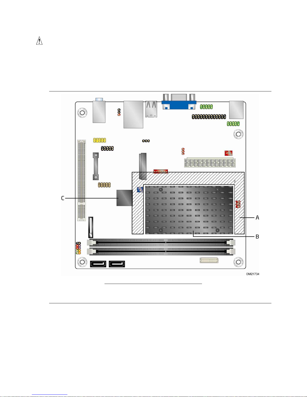
1.1.2 Board Layout
Figure 1 shows the location of the major components.
Product Description
Table 3 lists the components identified in Figure 1.
Figure 1. Major Board Components
13
Page 14

Intel Desktop Board D510MO Technical Product Specification
Table 3. Board Components Shown in Figure 1
Item/callout
from Figure 1
A
B
C
D
E
F
G
H
I
J
K
L
M
N
O
P
Q
R
S
T
U
V
W
X
Y
Z
AA
Descript
Back panel connectors
Serial port header (COM 1)
Parallel port header
Serial port header (COM 2)
LVDS inverter power voltage selection jumper (optional)
Chassis fan header
Power connector (2 x 12)
LVDS inverter power connector (optional)
Standby power LED
Intel Atom processor
LVDS inverter panel voltage selection header (optional)
DIMM channel A socket, DIMM 0
DIMM channel A socket, DIMM 1
LVDS panel connector (optional)
SATA connector 1
SATA connector 0
Front panel header
Battery
Front panel wireless activity LED header
Intel NM10 Express Chipset
Front panel USB header (with Intel Z-U130 USB Solid-State
Drive (or compatible device) support
PCI conventional bus connector
PCI Express x1 Mini Card connector
USB front panel header
Front panel audio header
BIOS setup configuration jumper block
S/PDIF header
ion
14
Page 15
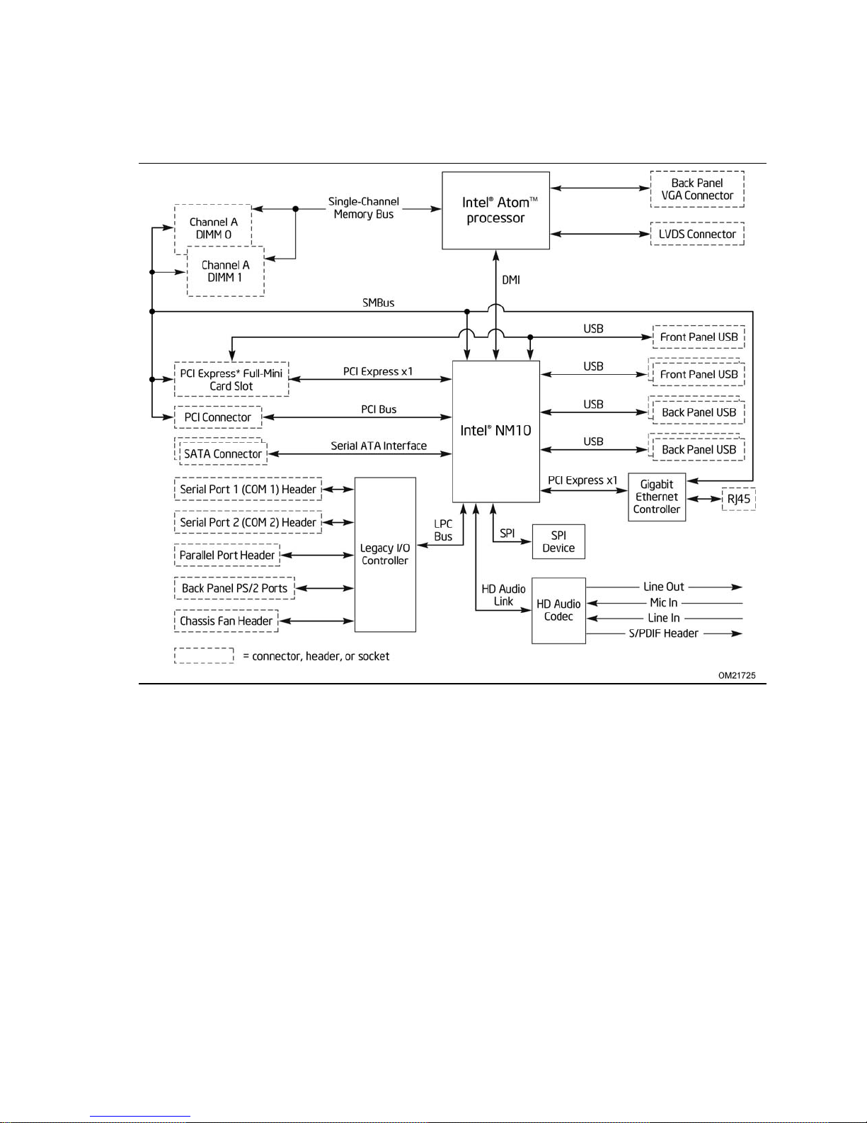
1.1.3 Block Diagram
Figure 2 is a block diagram of the major functional areas.
Product Description
Figure 2. Block Diagram
15
Page 16
Intel Desktop Board D510MO Technical Product Specification
1.2 Online Support
To find information about… Visit this World Wide Web site:
Intel Desktop Board D510MO http://www.intel.com/products/motherboard/510MO/index.htm
Desktop Board Support http://www.intel.com/support/motherboards/desktop
Available configurations for the Intel
Desktop Board D510MO
Chipset information http://www.intel.com/products/desktop/chipsets/index.htm
BIOS and driver updates http://downloadcenter.intel.com
Integration information http://www.intel.com/support/go/buildit
Tested memory http://www.intel.com/support/motherboards/desktop/sb/CS-
http://www.intel.com/products/motherboard/D510MO/index.htm
025414.htm
1.3 Processor
The board has a passively-cooled, soldered-down Dual-Core Intel Atom processor with
integrated graphics and integrated memory controller.
NOTE
The board is designed to be passively cooled in a properly ventilated chassis. Chassis
venting locations are recommended above the processor heatsink area for maximum
heat dissipation effectiveness.
For information about Refer to
Power supply connectors Section 2.2.2.3, page 50
16
Page 17

Product Description
1.3.1 Intel D510 Graphics Subsystem
1.3.1.1 Intel® Graphics Media Accelerator 3150 Graphics
Controller
The Intel GMA 3150 graphics controller features the following:
• 400 MHz core frequency
• High quality texture engine
⎯ DX9.0c* and OpenGL* 1.4 compliant
⎯ Hardware Pixel Shader 2.0
⎯ Vertex Shader Model 2.0
• 3D Graphics Rendering enhancements
⎯ 1.6 dual texture GigaPixel/s max fill rate
⎯ 16-bit and 32-bit color
⎯ Vertex cache
• Video
⎯ Software DVD at 30 fps full screen
⎯ DVMT support up to 256 MB
• Display
⎯ Supports analog displays up to 2048 x 1536 at 75 Hz refresh (QXGA)
⎯ Optionally supports LVDS display up to 1366 x 768 (single channel, 18 bpp)
⎯ Dual independent display support with LVDS option
For information about Refer to
Obtaining graphics software and utilities Section 1.2, page 16
17
Page 18
Intel Desktop Board D510MO Technical Product Specification
1.4 System Memory
The board has two 240-pin DDR2 DIMM sockets and supports the following memory
features:
• DDR2 SDRAM DIMMs with gold-plated contacts
• Unbuffered, single-sided or double-sided DIMMs
• 4 GB maximum total system memory
• Minimum total system memory: 256 MB
• Non-ECC DIMMs
• Serial Presence Detect
• DDR2 800 MHz and DDR2 667 MHz DIMMs
NOTE
Due to passively-cooled thermal constraints, system memory must have an operating
temperature rating of 85
The board is designed to be passively cooled in a properly ventilated chassis. Chassis
venting locations are recommended above the system memory area for maximum
heat dissipation effectiveness.
o
C.
NOTE
To be fully compliant with all applicable DDR2 SDRAM memory specifications, the
board should be populated with DIMMs that support the Serial Presence Detect (SPD)
data structure. This allows the BIOS to read the SPD data and program the chipset to
accurately configure memory settings for optimum performance. If non-SPD memory
is installed, performance and reliability may be impacted or the DIMMs may not
function under the determined frequency.
Table 4 lists the supported DIMM configurations.
Table 4. Supported Memory Configurations
DIMM
Capacity Configuration
256 MB SS 256 Mbit 32 M x 8/empty 8
256 MB SS 512 Mbit 32 M x 16/empty 4
512 MB DS 256 Mbit 32 M x 8/32 M x 8 16
512 MB SS 512 Mbit 64 M x 8/empty 8
512 MB SS 1 Gbit 64 M x 16/empty 4
1024 MB DS 512 Mbit 64 M x 8/64 M x 8 16
1024 MB SS 1 Gbit 128 M x 8/empty 8
2048 MB DS 1 Gbit 128 M x 8/128 M x 8 16
Note: In the second column, “DS” refers to double-sided memory modules (containing two rows of SDRAM)
and “SS” refers to single-sided memory modules (containing one row of SDRAM).
SDRAM
Density
SDRAM Organization
Front-side/Back-side
Number of SDRAM
Devices
18
Page 19

Product Description
1.5 Intel® NM10 Express Chipset
The Intel NM10 Express Chipset provides interfaces to the processor and the USB,
SATA, LPC, LAN, PCI, and PCIe interfaces. The Intel NM10 Express Chipset is a
centralized controller for the board’s I/O paths.
NOTE
The board is designed to be passively cooled in a properly ventilated chassis. Chassis
venting locations are recommended above the processor heatsink area for maximum
heat dissipation effectiveness.
For information about Refer to
The Intel NM10 Express chipset http://www.intel.com/products/desktop/chipsets/index.htm
Resources used by the chipset Chapter 2
1.5.1.1 Video Memory Allocation
Video memory is allocated from the total available system memory for the efficient
balancing of 2-D/3-D graphics performance and overall system performance. Dynamic
allocation of system memory to video memory is as follows:
• 256 MB total RAM results in 32 MB video RAM
• 512 MB total RAM results in 64 MB video RAM
• 1 GB total RAM results in 128 MB video RAM
• 2 GB total RAM results in 224 MB video RAM
1.5.1.2 Analog Display (VGA)
The VGA port supports analog displays. The maximum supported resolution is 2048 x
1536 (QXGA) at a 75 Hz refresh rate.
1.5.1.3 Optional Flat Panel Interface (LVDS)
The optional flat panel interface (LVDS) supports the following:
• Panel support up to UXGA (1366 x 768)
• 25 MHz to 112 MHz single–channel; @18 bpp
⎯ TFT panel type
• Panel fitting, panning, and center mode
• CPIS 1.5 compliant
• Spread spectrum clocking
• Panel power sequencing
• Integrated PWM interface for LCD backlight inverter control
19
Page 20

Intel Desktop Board D510MO Technical Product Specification
1.5.1.4 Configuration Modes
For monitors attached to the VGA port, video modes supported by this board are
based on the Extended Display Identification Data (EDID) protocol.
Video mode configuration for LVDS displays is supported as follows:
• Automatic panel identification via Extended Display Identification Data (EDID) for
LVDS panels supporting EDID protocol.
• Manual LVDS panel configuration through the BIOS setup page. This feature
allows the manual entry of critical panel settings (equivalent to the 18-byte
Detailed Timings Descriptor structure defined by the VESA EDID specification) for
non-EDID panel support.
In addition, BIOS setup provides the following configuration parameters for LVDS
displays:
• Screen Brightness: allows the end-user to set screen brightness for the display.
• Maintain Aspect Ratio: allows the end-user to select whether the native aspect
ratio is to be preserved during POST and before the video driver is loaded.
• LVDS Configuration Changes: allows the system integrator to “lock” critical settings
of the LVDS configuration to avoid end-users potentially rendering the display
unusable (refer to Note 1).
• Inverter Frequency and Polarity: allows the system integrator to set the operating
frequency and polarity of the panel inverter board.
• Minimum Inverter Current Limit (%): allows the system integrator to set minimum
PWM%, as appropriate, according to the power requirements of the LVDS display
and the selected inverter board.
NOTE
Support for LVDS configuration complies with the following:
1. “Unlocking” of critical settings of the LVDS configuration is supported via Intel
Integrator Toolkit’s command-line tool.
2. Critical settings of the LVDS configuration are not exposed through Intel Integrator
Toolkit or Intel
3. Critical settings of the LVDS configuration will not be overwritten by loading BIOS
setup defaults.
4. Critical settings of the LVDS configuration will be preserved across BIOS updates.
®
Integrator Assistant GUIs.
®
20
Page 21

Product Description
1.5.2 USB
The board provides up to seven USB 2.0 ports, supports UHCI and EHCI, and uses
UHCI- and EHCI-compatible drivers. The port arrangement is as follows:
• Four ports are implemented with stacked back panel connectors
• Three front panel ports (via two internal headers; one header (with one port)
supports an Intel
NOTE
One of the front panel USB headers supports an Intel Z-U130 USB Solid-State Drive
(or compatible device).
Computer systems that have an unshielded cable attached to a USB port may not
meet FCC Class B requirements, even if no device is attached to the cable. Use
shielded cable that meets the requirements for full-speed devices.
For information about Refer to
The location of the USB connectors on the back panel Figure 8, page 41
The location of the front panel USB headers Figure 10, page 43
®
Z-U130 USB Solid-State Drive (or compatible device)
1.5.3 SATA Support
The board provides two SATA interface connectors that support one device per
connector.
The board’s SATA controller offers independent SATA ports with a theoretical
maximum transfer rate of 3.0 Gbits/sec on each port. One device can be installed on
each port for a maximum of two SATA devices. A point-to-point interface is used for
host to device connections, unlike PATA which supports a master/slave configuration
and two devices on each channel.
For compatibility, the underlying SATA functionality is transparent to the operating
system. The SATA controller supports IDE and AHCI configuration and can operate in
both legacy and native modes. In legacy mode, standard ATA I/O and IRQ resources
are assigned (IRQ 14 and 15). In Native mode, standard PCI Conventional bus
resource steering is used. Native mode is the preferred mode for configurations using
the Windows* XP and Windows Vista* operating systems.
For information about Refer to
Obtaining AHCI driver Section 1.2, page 16
The location of the SATA connectors Figure 10, page 43
21
Page 22

Intel Desktop Board D510MO Technical Product Specification
1.6 Real-Time Clock Subsystem
A coin-cell battery (CR2032) powers the real-time clock and CMOS memory. When
the computer is not plugged into a wall socket, the battery has an estimated life of
three years. When the computer is plugged in, the standby current from the power
supply extends the life of the battery. The clock is accurate to ± 13 minutes/year at
25 ºC with 3.3 VSB applied.
NOTE
If the battery and AC power fail, custom defaults, if previously saved, will be loaded
into CMOS RAM at power-on.
When the voltage drops below a certain level, the BIOS Setup program settings stored
in CMOS RAM (for example, the date and time) might not be accurate. Replace the
battery with an equivalent one. Figure 1 on page 13 shows the location of the battery.
1.7 Legacy I/O Controller
The Legacy I/O Controller provides the following features:
• Two serial port headers
• One parallel port header with Extended Capabilities Port (ECP) and Enhanced
Parallel Port (EPP) support
• Serial IRQ interface compatible with serialized IRQ support for PCI Conventional
bus systems
• PS/2-style keyboard and mouse ports
• Intelligent power management, including a programmable wake-up event interface
• PCI Conventional bus power management support
The BIOS Setup program provides configuration options for the Legacy I/O controller.
1.7.1 Serial Port Headers
The serial port headers, COM 1 and COM 2, are implemented as two 10-pin headers on
the board. The serial port headers support data transfers at speeds up to
115.2 kbits/s with BIOS support.
For information about Refer to
The location of the serial port headers Figure 10, page 43
22
Page 23

Product Description
1.7.2 Parallel Port Header
The parallel port header is implemented as a 26-pin header on the board. Use the
BIOS Setup program to set the parallel port mode.
For information about Refer to
The location of the parallel port header Figure 10, page 43
1.8 LAN Subsystem
The LAN subsystem consists of the following:
• Intel NM10 Express Chipset
• Realtek 8111DL Gigabit Ethernet Controller for 10/100/1000 Mbits/sec Ethernet
LAN connectivity
• RJ-45 LAN connector with integrated status LEDs
Additional features of the LAN subsystem include:
• CSMA/CD protocol engine
• LAN connect interface that supports the ethernet controller
• PCI Conventional bus power management
⎯ Supports ACPI technology
⎯ Supports LAN wake capabilities
1.8.1 LAN Subsystem Drivers
LAN drivers are available from Intel’s World Wide Web site.
For information about Refer to
Obtaining LAN drivers Section 1.2, page 16
23
Page 24
Intel Desktop Board D510MO Technical Product Specification
1.8.2 RJ-45 LAN Connector with Integrated LEDs
Two LEDs are built into the RJ-45 LAN connector (shown in Figure 3).
Figure 3. LAN Connector LED Locations
Table 5 describes the LED states when the board is powered up and the
10/100/1000 Mbits/sec LAN subsystem is operating.
Table 5. LAN Connector LED States
LED Color State Condition
Activity (A)
Speed (B)
Green Blinking LAN activity occurring
N/A Off 10 Mb/s data rate
Green On 100 Mb/s data rate
Yellow On 1000 Mb/s data rate
24
Page 25

Product Description
1.9 Audio Subsystem
The board supports the Intel High Definition Audio subsystem. The audio subsystem
consists of the following:
• Intel NM10 Express Chipset
• Realtek ALC662 audio codec
The audio subsystem has the following features:
• Advanced jack sense for the back panel audio jacks that enables the audio codec to
recognize the device that is connected to an audio port. The back panel audio
jacks are capable of retasking according to the user’s definition, or can be
automatically switched depending on the recognized device type.
• Front panel Intel HD Audio and AC ’97 audio support
• 3-port analog audio out stack
• Internal S/PDIF out header
• Windows Vista Basic certification
• A signal-to-noise (S/N) ratio of 95 dB
• Independent 5.1 audio playback from back panel connectors and stereo playback
from the Intel High Definition Audio front panel header.
• 4+2 channel in multi-streaming mode
Table 6 lists the supported functions of the front panel and back panel audio jacks.
Table 6. Audio Jack Support
Audio Jack
Front panel – Green No Yes No No No Yes
Front panel – Pink No No No No Yes No
Back panel – Blue Yes No Yes No No No
Back panel – Green No Yes No No No Yes
Back panel – Pink No No No Yes Yes No
Line In
Line/
Front Out Rear Out
Center/
LFE
MIC
Headphones
25
Page 26
Intel Desktop Board D510MO Technical Product Specification
1.9.1 Audio Subsystem Software
Audio software and drivers are available from Intel’s World Wide Web site.
For information about Refer to
Obtaining audio software and drivers Section 1.2, page 16
1.9.2 Audio Connectors and Headers
The board contains audio connectors and headers on both the back panel and the
component side of the board. The component-side audio headers include the
following:
• Front panel audio (a 2 x 5-pin header that provides mic in and line out signals for
front panel audio connectors)
• S/PDIF audio 1 x 3-pin header
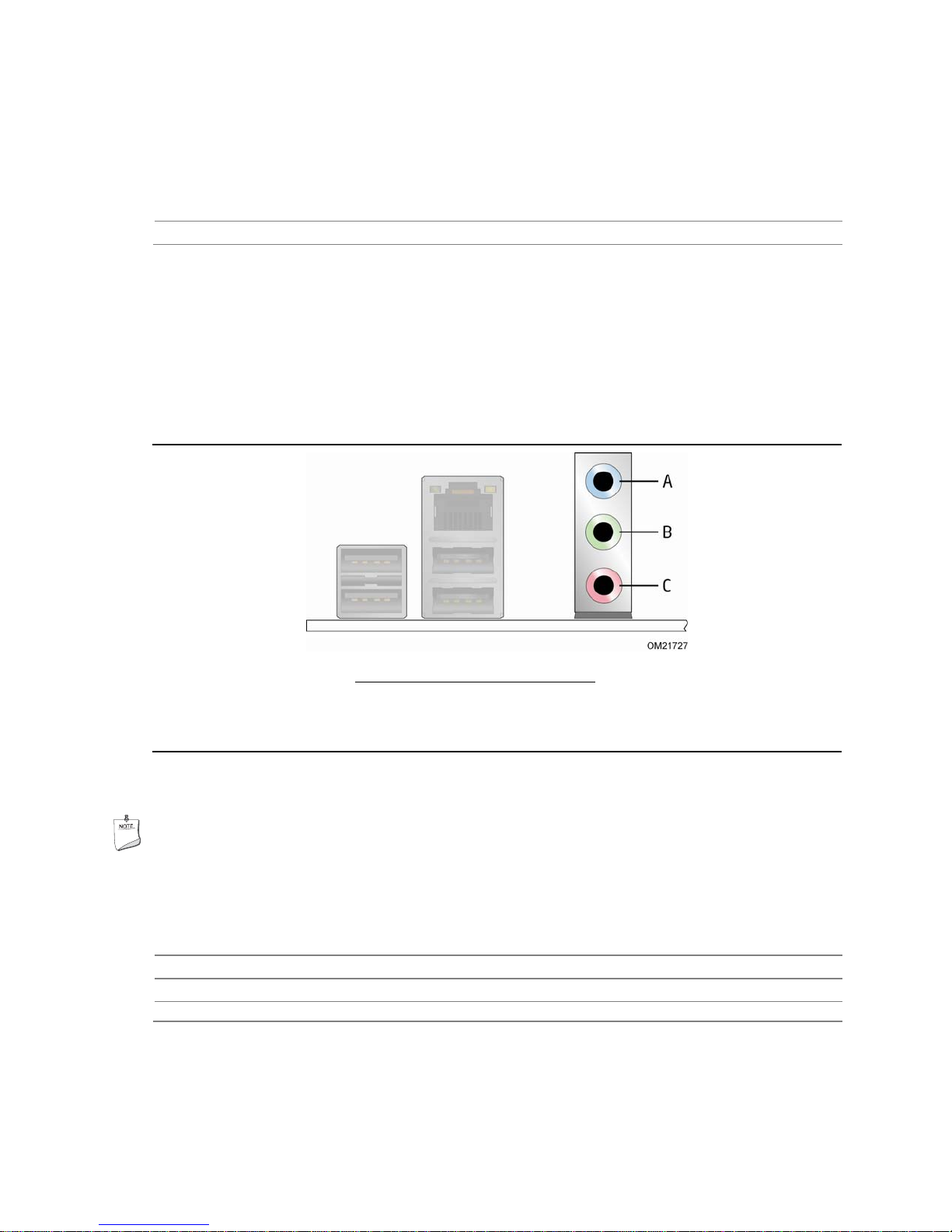
Item Description
A Line in
B Line out
C Mic in
Figure 4. Back Panel Audio Connectors
NOTE
The back panel audio line out connector is designed to power headphones or amplified
speakers only. Poor audio quality occurs if passive (non-amplified) speakers are
connected to this output.
For information about Refer to
The locations of the front panel audio header and S/PDIF audio header Figure 10, page 43
The signal names of the front panel audio header and S/PDIF header Section 2.2.2.1. page 45
The back panel audio connectors Figure 4. page 26
26
Page 27

Product Description
1.10 Hardware Management Subsystem
The hardware management features enable the board to be compatible with the Wired
for Management (WfM) specification. The board has several hardware management
features, including the following:
• Thermal and voltage monitoring
• Chassis intrusion detection
1.10.1 Hardware Monitoring
The hardware monitoring and fan control subsystem is based on the Winbond
W83627THG-I device, which supports the following:
• Processor and system ambient temperature monitoring
• Chassis fan speed monitoring
• Power monitoring of +12 V, +5 V, +5 Vstdby, +3.3 V, and +VCCP
• SMBus interface
27
Page 28
Intel Desktop Board D510MO Technical Product Specification
1.10.2 Thermal Monitoring
Figure 5 shows the locations of the thermal sensors and fan header.
Item Description
A Chassis fan header
B Thermal diode, located on the processor die
C Remote thermal sensor
Figure 5. Thermal Sensors and Fan Header
28
Page 29

Product Description
1.11 Power Management
Power management is implemented at several levels, including:
• Software support through Advanced Configuration and Power Interface (ACPI)
• Hardware support:
⎯ Power connector
⎯ Fan header
⎯ LAN wake capabilities
⎯ Instantly Available PC technology
⎯ Wake from USB
⎯ Wake from PS/2 devices
⎯ Power Management Event signal (PME#) wake-up support
⎯ WAKE# signal wake-up support
1.11.1 ACPI
ACPI gives the operating system direct control over the power management and Plug
and Play functions of a computer. The use of ACPI with the board requires an
operating system that provides full ACPI support. ACPI features include:
• Plug and Play (including bus and device enumeration)
• Power management control of individual devices, add-in boards (some add-in
boards may require an ACPI-aware driver), video displays, and hard disk drives
• Methods for achieving less than 15-watt system operation in the power-on/standby
sleeping state
• A Soft-off feature that enables the operating system to power-off the computer
• Support for multiple wake-up events (see Table 9 on page 31)
• Support for a front panel power and sleep mode switch
Table 7 lists the system states based on how long the power switch is pressed,
dependi
g on how ACPI is configured with an ACPI-aware operating system.
n
Table 7. Effects of Pressing the Power Switch
If the system is in this
state…
Off
(ACPI G2/G5 – Soft off)
On
(ACPI G0 – working state)
On
(ACPI G0 – working state)
Sleep
(ACPI G1 – sleeping state)
Sleep
(ACPI G1 – sleeping state)
…and the power switch
is pressed for
Less than four seconds Power-on
Less than four seconds Power-off
More than four seconds Fail safe power-off
Less than four seconds Wake-up
More than four seconds Power-off
…the system enters this state
(ACPI G0 – working state)
(ACPI G2/G5 – Soft off)
(ACPI G2/G5 – Soft off)
(ACPI G0 – working state)
(ACPI G2/G5 – Soft off)
29
Page 30

Intel Desktop Board D510MO Technical Product Specification
1.11.1.1 System States and Power States
Under ACPI, the operating system directs all system and device power state
transitions. The operating system puts devices in and out of low-power states based
on user preferences and knowledge of how devices are being used by applications.
Devices that are not being used can be turned off. The operating system uses
information from applications and user settings to put the system as a whole into a
low-power state.
Table 8 lists the power states supported by the board along with the associated
system power targets. See the AC
various system and power states.
Table 8. Power States and Targeted System Power
PI specificat
ion for a complete description of the
Global
States
G0 – working
state
G1 – sleeping
state
G1 – sleeping
state
G1 – sleeping
state
G2/S5 S5 – Soft off.
G3 –
mechanical off.
AC power is
disconnected
from the
computer.
Notes:
1. Total system power is dependent on the system configuration, including add-in boards and peripherals
powered by the system’s power supply.
2. Dependent on the standby power consumption of wake-up devices used in the system.
Sleeping States
S0 – working C0 – working D0 – working
S1 – Processor
stopped
S3 – Suspend to
RAM. Context
saved to RAM.
S4 – Suspend to
disk. Context
saved to disk.
Context not saved.
Cold boot is
required.
No power to the
system.
Processor
States
C1 – stop
grant
No power D3 – no power
No power D3 – no power
No power D3 – no power
No power D3 – no power for
Device States
state.
D1, D2, D3 –
device
specification
specific.
except for
wake-up logic.
except for
wake-up logic.
except for
wake-up logic.
wake-up logic,
except when
provided by
battery or
external source.
Targeted System
Power
Full power > 30 W
5 W < power < 52.5 W
Power < 5 W
Power < 5 W
Power < 5 W
No power to the system.
Service can be performed
safely.
(Note 1)
(Note 2)
(Note 2)
(Note 2)
30
Page 31

Product Description
1.11.1.2 Wake-up Devices and Events
Table 9 lists the devices or specific events that can wake the computer from specific
states.
Table 9. Wake-up Devices and Events
These devices/events can wake up the computer… …from this state
LAN S1, S3, S4, S5
PME# signal S1, S3, S4, S5
Wake# signal S1, S3, S4, S5
Power switch S1, S3, S4, S5
RTC alarm S4, S5
Serial port S1, S3
USB S1, S3
PS/2 devices S1, S3, S4, S5
Notes:
1. S4 implies operating system support only. Wake from S5 must include wake after loss of power.
2. USB ports are turned off during S4/S5 states.
3. Wake# signal must be controllable by the BIOS (enable/disable option).
4. PS/2 wake from S5 should have a selection in the BIOS to enable wake from a combination key
(Alt + Print Screen) or the keyboard power button.
(Note 1)
(Note 2)
(Note 1)
(Note 1)
(Notes 1 and 3)
(Note 1)
(Notes 1 and 4)
NOTE
The use of these wake-up events from an ACPI state requires an operating system
that provides full ACPI support. In addition, software, drivers, and peripherals must
fully support ACPI wake events.
31
Page 32

Intel Desktop Board D510MO Technical Product Specification
1.11.2 Hardware Support
The board provides several power management hardware features, including:
• Power connector
• Fan header
• LAN wake capabilities
• Instantly Available PC technology
• Wake from USB
• Wake from PS/2 devices
• Power Management Event signal (PME#) wake-up support
• WAKE# signal wake-up support
• +5V Standby Power Indicator LED
LAN wake capabilities and Instantly Available PC technology require power from the
+5 V standby line.
NOTE
The use of Wake from USB technologies from an ACPI state requires an operating
system that provides full ACPI support.
1.11.2.1 Fan Header
The function/operation of the fan header is as follows:
• The fan is on when the board is in the S0 state.
• The fan is off when the board is off or in the S3, S4, or S5 state.
• The chassis fan header supports closed-loop fan control that can adjust the fan
speed and is wired to a fan tachometer input.
• The fan header supports +12 V, 3-wire fans at 1 A maximum.
For information about Refer to
The locations of the fan header and thermal sensors Figure 5, page 28
The signal names of the chassis fan header Table 16, page 45
1.11.2.2 LAN Wake Capabilities
LAN wake capabilities enable remote wake-up of the computer through a network.
The LAN subsystem network adapter monitors network traffic at the Media
Independent Interface. The board supports LAN wake capabilities with ACPI in the
following ways:
• By Ping
• By Magic Packet
Upon detecting the configured wake packet type, the LAN subsystem asserts a wakeup signal that powers up the computer.
32
Page 33

Product Description
1.11.2.3 Instantly Available PC Technology
Instantly Available PC technology enables the board to enter the ACPI S3 (Suspend-toRAM) sleep-state. While in the S3 sleep-state, the computer will appear to be off (the
hard drive(s) and fan will power off, the front panel LED will blink). When signaled by
a wake-up device or event, the system quickly returns to its last known state. Table 9
on page 31 lists the devices and events that can wake the computer from the
S3 state.
The board supports the PC
boards that also support this specification can participate in power management and
can be used to wake the computer.
The use of Instantly Available PC technology requires operating system support and
PCI 2.3 compliant add-in cards and drivers.
I Bus Power Managem
ent Interface Specification. Add-in
1.11.2.4 Wake from USB
USB bus activity wakes the computer from an ACPI S1 or S3 state.
NOTE
Wake from USB requires the use of a USB peripheral that supports Wake from USB
and support in the operating system.
1.11.2.5 PME# Signal Wake-up Support
When the PME# signal on the PCI bus is asserted, the computer wakes from an ACPI
S1, S3, S4, or S5 state (with Wake on PME enabled in the BIOS).
1.11.2.6 Wake from PS/2 Devices
PS/2 keyboard activity wakes the computer from an ACPI S1, S3, S4, or S5 state.
However, when the computer is in an ACPI S4 or S5 state, the only PS/2 activity that
will wake the computer is the Alt + Print Screen or the Power Key available only on
some keyboards.
1.11.2.7 WAKE# Signal Wake-up Support
When the WAKE# signal on the PCI Express bus is asserted, the computer wakes from
an ACPI S1, S3, S4, or S5 state.
1.11.2.8 Wake from Serial Port
Serial Port activity wakes the computer from an ACPI S1 or S3 state.
33
Page 34
Intel Desktop Board D510MO Technical Product Specification
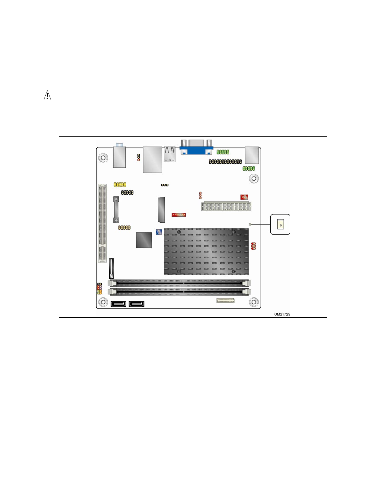
1.11.2.9 +5 V Standby Power Indicator LED
The +5 V standby power indicator LED shows that power is still present even when the
computer appears to be off. Figure 6 shows the location of the standby power
indicator LED.
CAUTION
If AC power has been switched off and the standby power indicator is still lit,
disconnect the power cord before installing or removing any devices connected to the
board. Failure to do so could damage the board and any attached devices.
Figure 6. Location of the Standby Power Indicator LED
34
Page 35

Product Description
1.11.3 ENERGY STAR*, E-Standby, and EuP Compliance
The US Department of Energy and the US Environmental Protection Agency have
continually revised the ENERGY STAR requirements. Intel has worked directly with
these two governmental agencies in the definition of new requirements. This Intel
Desktop Board meets the ENERGY STAR requirements listed in Table 10 when used in
corresponding system configurations.
NOTE
Energy Star compliance is based at the system level not the board level. Use of an
Intel Desktop Board alone does not guarantee Energy Star compliance.
Table 10. ENERGY STAR Requirements
ENERGY STAR
Specification Computer Type
v4.0 Desktop Computer
v4.0 Integrated Computer
v5.0 Desktop Computer
v5.0 Integrated Desktop
Computer
v5.0 Thin Client Off Mode
For information about Refer to
ENERGY STAR requirements and recommended configurations http://www.intel.com/go/energystar
Req States
Idle State (Cat A)
Sleep Mode
Standby Level
Off Mode
Sleep Mode
Idle State
Active State
Sleep Mode
Idle State (Cat B)
Capability
Adjustments
With and without
WOL (Sleep,
Standby)
With and without
additional internal
storage
With and without
WOL (Sleep,
Standby)
TEC Criteria
N/A
Cat A under
“desktop
conventional” and
“desktop
proxying”
operational mode
weightings
N/A
Intel Desktop Board D510MO also meets the following international program
requirements:
• Korea E-Standby
• European Union EuP
35
Page 36

Intel Desktop Board D510MO Technical Product Specification
36
Page 37

2 Technical Reference
2.1 Memory Map
2.1.1 Addressable Memory
The board utilizes 4 GB of addressable system memory. Typically the address space
that is allocated for PCI Conventional bus add-in cards, PCI Express configuration
space, BIOS (SPI Flash), and chipset overhead resides above the top of DRAM (total
system memory). On a system that has 4 GB of system memory installed, it is not
possible to use all of the installed memory due to system address space being
allocated for other system critical functions. These functions include the following:
• BIOS/ SPI Flash (4 MB)
• Local APIC (19 MB)
• Direct Media Interface (40 MB)
• Front side bus interrupts (17 MB)
• GMCH base address registers, internal graphics ranges
• Memory-mapped I/O that is dynamically allocated for PCI Conventional add-in
cards
37
Page 38

Intel Desktop Board D510MO Technical Product Specification
The amount of installed memory that can be used will vary based on add-in cards and
BIOS settings. Figure 7 shows a schematic of the system memory
map. All installed
system memory can be used when there is no overlap of system addresses.
Figure 7. Detailed System Memory Address Map
38
Page 39

Table 11 lists the system memory map.
Table 11. System Memory Map
Technical Reference
Address Range
(decimal)
1024 K - 4096 K 100000 - 400000 4096 MB Extended memory
960 K - 1024 K F0000 - FFFFF 64 KB Runtime BIOS
896 K - 960 K E0000 - EFFFF 64 KB Reserved
800 K - 896 K C8000 - DFFFF 96 KB Potential available high DOS
640 K - 800 K A0000 - C7FFF 160 KB Video memory and BIOS
639 K - 640 K 9FC00 - 9FFFF 1 KB Extended BIOS data (movable by
512 K - 639 K 80000 - 9FBFF 127 KB Extended conventional memory
0 K - 512 K 00000 - 7FFFF 512 KB Conventional memory
Address Range
(hex)
Size
Description
memory (open to the PCI bus).
Dependent on video adapter used.
memory manager software)
39
Page 40

Intel Desktop Board D510MO Technical Product Specification
2.2 Connectors and Headers
CAUTION
Only the following connectors/headers have overcurrent protection: Back panel and
front panel USB and PS/2.
The other internal connectors/headers are not overcurrent protected and should
connect only to devices inside the computer’s chassis, such as fans and internal
peripherals. Do not use these connectors/headers to power devices external to the
computer’s chassis. A fault in the load presented by the external devices could cause
damage to the computer, the power cable, and the external devices themselves.
NOTE
Computer systems that have an unshielded cable attached to a USB port may not
meet FCC Class B requirements, even if no device is attached to the cable. Use
shielded cable that meets the requirements for full-speed devices.
This section describes the board’s connectors and headers. The connectors and
headers can be divided into these groups:
• Back panel I/O connectors (see page 41)
• Component-side connectors and headers (see page 43)
40
Page 41
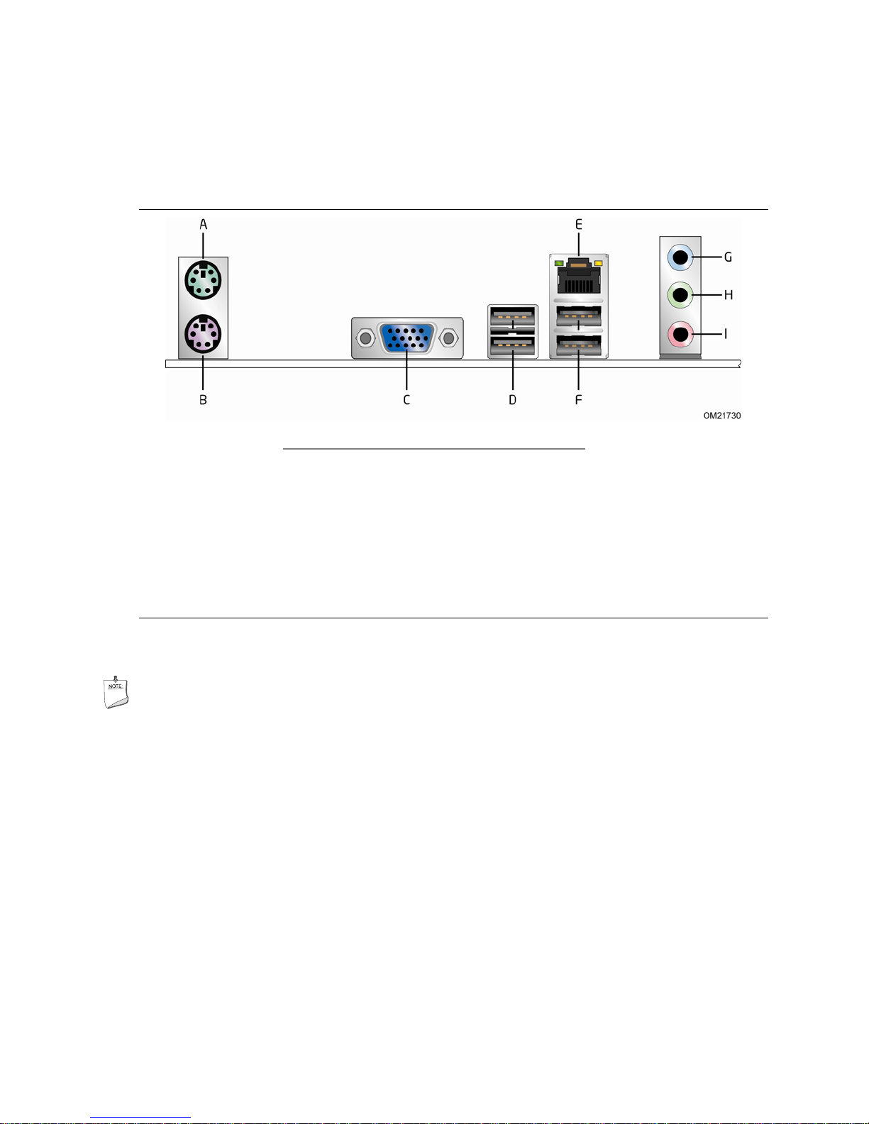
2.2.1 Back Panel
2.2.1.1 Back Panel Connectors
Figure 8 shows the location of the back panel connectors.
Item Description
A PS/2 keyboard/mouse connector
B PS/2 keyboard/mouse connector
C VGA port
D USB ports
E LAN connector (RJ-45)
F USB ports
G Line in
H Line out
I Mic in
Technical Reference
Figure 8. Back Panel Connectors
NOTE
The back panel audio line out connector is designed to power headphones or amplified
speakers only. Poor audio quality occurs if passive (non-amplified) speakers are
connected to this output.
41
Page 42
Intel Desktop Board D510MO Technical Product Specification
2.2.1.2 I/O Shield
The I/O shield provided with the board allows access to all back panel connectors and
is compatible with standard mini-ITX and microATX chassis. As an added benefit for
system configurations with wireless PCI Express Mini Card solutions, the I/O shield
also provides pre-cut holes for user installation of up to three external wireless
antennas. Figure 9 shows an I/O shield reference diagram.
Figure 9. I/O Shield Reference Diagram
42
Page 43
Technical Reference
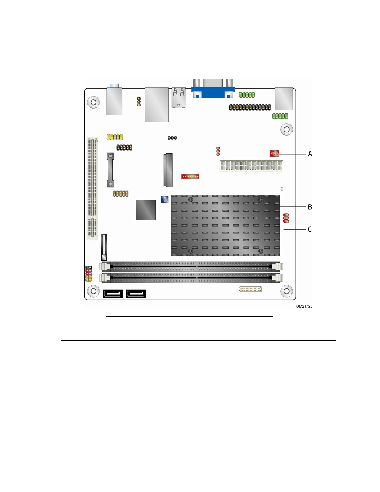
2.2.2 Component-side Connectors and Headers
Figure 10 shows the locations of the component-side connectors and headers.
Figure 10. Component-side Connectors and Headers
43
Page 44

Intel Desktop Board D510MO Technical Product Specification
Table 12 lists the component-side connectors and headers identified in Figure 10.
Table 12. Component-side Connectors and Headers Shown in Figure 10
Item/callout
from Figure 10 Descript
A
B
C
D
E
F
G
H
I
J
K
L
M
N
O
P
Q
R
S/PDIF header
Serial port header (COM 1)
Parallel port header
Serial port header (COM 2)
LVDS inverter power voltage selection jumper (optional)
Chassis fan header
Main power connector (2 x 12)
LVDS inverter power connector (optional)
LVDS inverter panel voltage selection header (optional)
LVDS panel connector (optional)
SATA connector 1
SATA connector 0
Front panel header
Front panel wireless activity LED header
Front panel USB header (with Intel Z-U130 USB Solid-State Drive, or compatible
device, support)
PCI conventional bus connector
USB front panel header
Front panel audio header
ion
44
Page 45

Technical Reference
2.2.2.1 Signal Tables for the Connectors and Headers
Table 13. Serial Port Header (COM 1 and COM 2)
Pin Signal Name Pin Signal Name
1 DCD (Data Carrier Detect) 2 RXD# (Receive Data)
3 TXD# (Transmit Data) 4 DTR (Data Terminal Ready)
5 Ground 6 DSR (Data Set Ready)
7 RTS (Request To Send) 8 CTS (Clear To Send)
9 RI (Ring Indicator) 10 Key (no pin)
Table 14. LVDS Data Connector - 30-Pin (Optional)
Pin
1 LA_CLKN LVDS Channel A diff
3 LA_CLKP LVDS Channel A diff
5 EDID_3.3V Power for EDID ROM 6 EDID_GND Ground for EDID signaling
7 LA_DATAN0 LVDS Channel A diff
9 LA_DATAP0 LVDS Channel A diff
11 LA_DATAN1 LVDS Channel A diff
13 LA_DATAP1 LVDS Channel A diff
15 GND Ground 16 GND Ground
17 LA_DATAN2 LVDS Channel A diff
19 LA_DATAP2 LVDS Channel A diff
21 GND Ground 22 GND Ground
23 GND Ground 24 GND Ground
25 3.3 V/5 V/12 V Selectable LCD
27 3.3 V/5 V/12 V Selectable LCD
29 EDID_CLK EDID/DDC clock
Signal
Name
Description
clock output negative
clock output positive
data output –
negative
data output –
positive
data output –
negative
data output –
positive
data output –
negative
data output –
positive
power output
power output
signal
Pin
2 NC
4 NC
8 NC
10 NC
12 NC
14 NC
18 NC
20 NC
26 3.3 V/5 V/12 V Selectable LCD power
28 3.3 V/5 V/12 V Selectable LCD power
30 EDID_DATA EDID/DDC data signal
Signal
Name
Description
output
output
45
Page 46

Intel Desktop Board D510MO Technical Product Specification
Table 15. LVDS Panel Voltage Selection Jumper (Optional)
Voltage Jumper Setting Configuration
3.3 V 2 and 4
5 V 6 and 4
12 V 3 and 4
Jumper position for 3.3 V (default)
Jumper position for 5 V
Jumper position for 12 V
Table 16. Chassis Fan Header
Pin Signal Name
1 Ground
2 +12 V (PWM controlled pulses)
3 Tach
Table 17. SATA Connectors
Pin Signal Name
1 Ground
2 TXP
3 TXN
4 Ground
5 RXN
6 RXP
7 Ground
46
Page 47
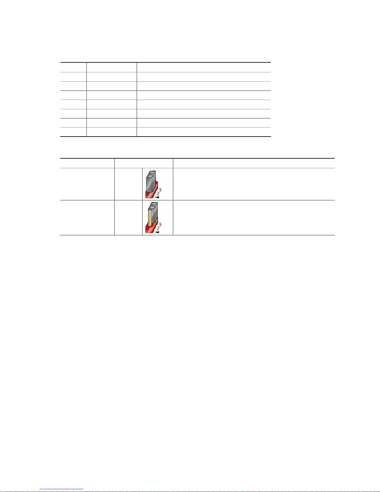
Table 18. LVDS Inverter Power Connector (Optional)
Pin Signal Name Description
1 GND Ground
2 GND Ground
3 5 V/12 V Inverter power
4 5 V/12 V Inverter power
5 INV_RATING Inverter rating
6 BKLT_PWM Backlight PWM
7 BKLT_EN Backlight enable
Table 19. LVDS Inverter Power Voltage Selection Jumper (Optional)
Voltage Jumper Setting Configuration
5 V 1 and 2
12 V 3 and 2
Jumper position for 5 V (default)
Jumper position for 12 V
Technical Reference
47
Page 48

Intel Desktop Board D510MO Technical Product Specification
Table 20. Parallel Port Header
Pin Standard Signal Name ECP Signal Name EPP Signal Name
1 STROBE# STROBE# WRITE#
2 AUTOFD# AUTOFD#, HOSACK DATASTB#
3 PD0 PD0 PD0
4 FAULT# FAULT#, PERIPHREQST# FAULT#
5 PD1 PD1 PD1
6 INT# INT#, REVERSERQST# RESET#
7 PD2 PD2 PD2
8 SLCTIN# SLCTIN# ADDRSTB#
9 PD3 PD3 PD3
10 GROUND GROUND GROUND
11 PD4 PD4 PD4
12 GROUND GROUND GROUND
13 PD5 PD5 PD5
14 GROUND GROUND GROUND
15 PD6 PD6 PD6
16 GROUND GROUND GROUND
17 PD7 PD7 PD7
18 GROUND GROUND GROUND
19 ACK# ACK# INTR
20 GROUND GROUND GROUND
21 BUSY BUSY#, PERIPHACK WAIT#
22 GROUND GROUND GROUND
23 PERROR PE, ACKREVERSE# PE
24 GROUND GROUND GROUND
25 SELECT SELECT SELECT
26 KEY (no pin) KEY (no pin) KEY (no pin)
Table 21. Front Panel Wireless Activity LED Header
Pin Signal Name
1 LED (+)
2 Ground
Table 22. S/PDIF Header
Pin Signal Name
1 VCC (5 V)
2 S/PDIF out
3 Ground
48
Page 49

Table 23. Front Panel Audio Header for Intel HD Audio
Pin Signal Name Pin Signal Name
1 [Port 1] Left channel 2 Ground
3 [Port 1] Right channel 4 PRESENCE# (Dongle present)
5 [Port 2] Right channel 6 [Port 1] SENSE_RETURN
7 SENSE_SEND (Jack detection) 8 Key (no pin)
9 [Port 2] Left channel 10 [Port 2] SENSE_RETURN
Table 24. Front Panel Audio Header for AC ’97 Audio
Pin Signal Name Pin Signal Name
1 MIC 2 AUD_GND
3 MIC_BIAS 4 AUD_GND
5 FP_OUT_R 6 FP_RETURN_R
7 AUD_5V 8 KEY (no pin)
9 FP_OUT_L 10 FP_RETURN_L
Technical Reference
Table 25. Front Panel USB Header
Pin Signal Name Pin Signal Name
1 +5 VDC 2 +5 VDC
3 D- 4 D5 D+ 6 D+
7 Ground 8 Ground
9 KEY (no pin) 10 No Connect
Table 26. Front Panel USB Header (with Intel Z-U130 USB Solid-State Drive,
or Compatible Device, Support)
Pin Signal Name Pin Signal Name
1 +5 VDC 2 NC
3 D- 4 NC
5 D+ 6 NC
7 Ground 8 NC
9 KEY (no pin) 10 LED#
49
Page 50

Intel Desktop Board D510MO Technical Product Specification
2.2.2.2 Add-in Card Connectors
The board has the following add-in card connectors:
• PCI Express x1 Mini Card (rev 1.2 compliant) connector
• PCI Conventional (rev 2.3 compliant) bus connector
Note the following considerations for the PCI Conventional bus connector:
• The PCI Conventional bus connector is bus master capable.
• SMBus signals are routed to the PCI Conventional bus connector. This enables PCI
Conventional bus add-in boards with SMBus support to access sensor data on the
board. The specific SMBus signals are as follows:
⎯ The SMBus clock line is connected to pin A40.
⎯ The SMBus data line is connected to pin A41.
The PCI Conventional bus connector also supports single-slot and dual-slot riser cards
for use of up to two bus master PCI expansion cards. In order to support two PCI bus
master expansion cards, the riser card must support the following PCI signal routing:
• Pin A11: additional 33 MHz PCI clock
• Pin B10: additional PCI Request signal (i.e., PREQ#2)
• Pin B14: additional PCI Grant signal (i.e., GNT#2)
2.2.2.3 Power Supply Connector
The board has a 2 x 12 power connector (see Table 27). This board requires a TFX12V
or SFX12V power supply.
Table 27. Power Connector
Pin Signal Name Pin Signal Name
1 +3.3 V 13 +3.3 V
2 +3.3 V 14 -12 V
3 Ground 15 Ground
4 +5 V 16 PS-ON# (power supply remote on/off)
5 Ground 17 Ground
6 +5 V 18 Ground
7 Ground 19 Ground
8 PWRGD (Power Good) 20 No connect
9 +5 V (Standby) 21 +5 V
10 +12 V 22 +5 V
11 +12 V 23 +5 V
12 No connect 24 Ground
50
Page 51

Technical Reference
2.2.2.4 Front Panel Header
This section describes the functions of the front panel header. Table 28 lists the signal
names of the front panel header. Figure 11 is a connection diagram for the front panel
header.
Table 28. Front Panel Header
Pin Signal
In/
Out Description
Pin Signal
In/
Out Description
Hard Drive Activity LED Power LED
1 HD_PWR Out Hard disk LED
pull-up to +5 V
3 HDA# Out Hard disk active
LED
2 HDR_BLNK_GRN Out Front panel green
LED
4 HDR_BLNK_YEL Out Front panel yellow
LED
Reset Switch On/Off Switch
5 Ground Ground 6 FPBUT_IN In Power switch
7 FP_RESET# In Reset switch 8 Ground Ground
Power Not Connected
9 +5 V Power 10 N/C Not connected
Figure 11. Connection Diagram for Front Panel Header
51
Page 52

Intel Desktop Board D510MO Technical Product Specification
2.2.2.4.1 Hard Drive Activity LED Header
Pins 1 and 3 can be connected to an LED to provide a visual indicator that data is
being read from or written to a hard drive. Proper LED function requires one of the
following:
• SATA storage device connected to an onboard SATA connector
• Intel Z-U130 USB Solid State Drive (or compatible device) connected to the
designated Z-U130 front panel USB header
2.2.2.4.2 Reset Switch Header
Pins 5 and 7 can be connected to a momentary single pole, single throw (SPST) type
switch that is normally open. When the switch is closed, the board resets and runs the
POST.
2.2.2.4.3 Power/Sleep LED Header
Pins 2 and 4 can be connected to a single- or dual-color LED. Table 29 shows the
defaul
t states for a si
ngle-color LED.
Table 29. States for a One-Color Power LED
LED State Description
Off Power off/hibernate (S5/S4)
Blinking Sleeping (S3)
Steady Green Running/Away (S0/S1)
NOTE
The LED states listed in Table 29 are default settings that can be modified through
BIOS setup. Systems built with a dual-color front panel power LED can also use
alternate color state options.
2.2.2.4.4 Power Switch Header
Pi
ns 6 and 8 can be connected to a front panel momentary-contact power switch. The
switch must pull the SW_ON# pin to ground for at least 50 ms to signal the power
supply circuitry to switch on or off. (The time requirement is due to internal debounce
circuitry on the board.) At least two seconds must pass before the power supply
circuitry will recognize another on/off signal.
52
Page 53

Technical Reference
2.2.2.5 Front Panel USB Headers
Figure 12 and Figure 13 are connection diagrams for the front panel USB headers.
NOTE
• The +5 VDC power on the USB headers is fused.
• Use only a front panel USB connector that conforms to the USB 2.0 specification
for high-speed USB devices.
Figure 12. Connection Diagram for Front Panel USB Header
Figure 13. Connection Diagram for Front Panel USB Header
(with Intel Z-U130 USB Solid-State Drive, or Compatible Device, Support)
53
Page 54

Intel Desktop Board D510MO Technical Product Specification
2.3 BIOS Configuration Jumper Block
CAUTION
Do not move the jumper with the power on. Always turn off the power and unplug the
power cord from the computer before changing a jumper setting. Otherwise, the
board could be damaged.
Figure 14 shows the location of the jumper block. The jumper determines the BIOS
Setup program’s mode. Table 30 lists the jumper settings for the three modes:
normal
, confi
gure, and recovery.
Figure 14. Location of the BIOS Configuration Jumper Block
54
Page 55
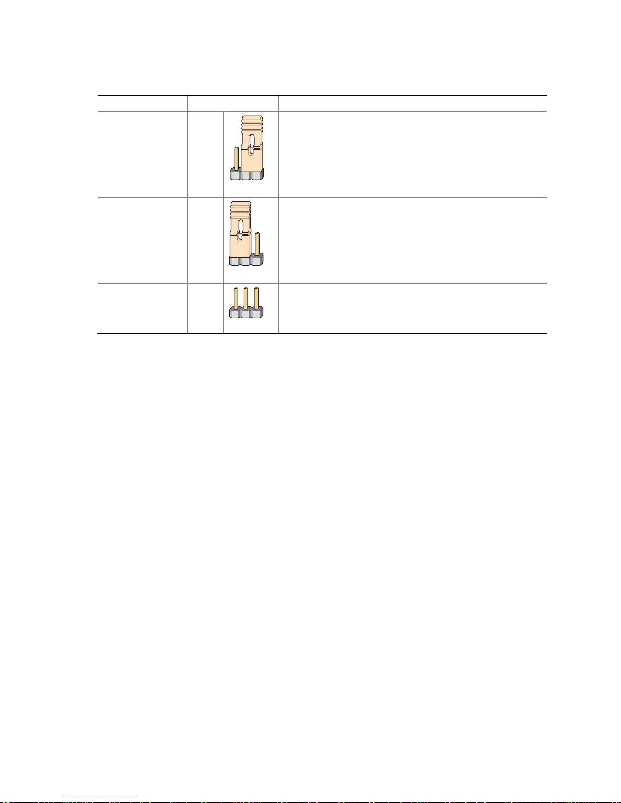
Table 30. BIOS Configuration Jumper Settings
Function/Mode Jumper Setting Configuration
Normal 1-2
The BIOS uses current configuration information and
passwords for booting.
Technical Reference
321
Configure 2-3
321
Recovery None
321
After the POST runs, Setup runs automatically. The
maintenance menu is displayed.
The BIOS attempts to recover the BIOS configuration. See
Section 3.7 for more information on BIOS recovery.
55
Page 56

Intel Desktop Board D510MO Technical Product Specification
2.4 Mechanical Considerations
2.4.1 Form Factor
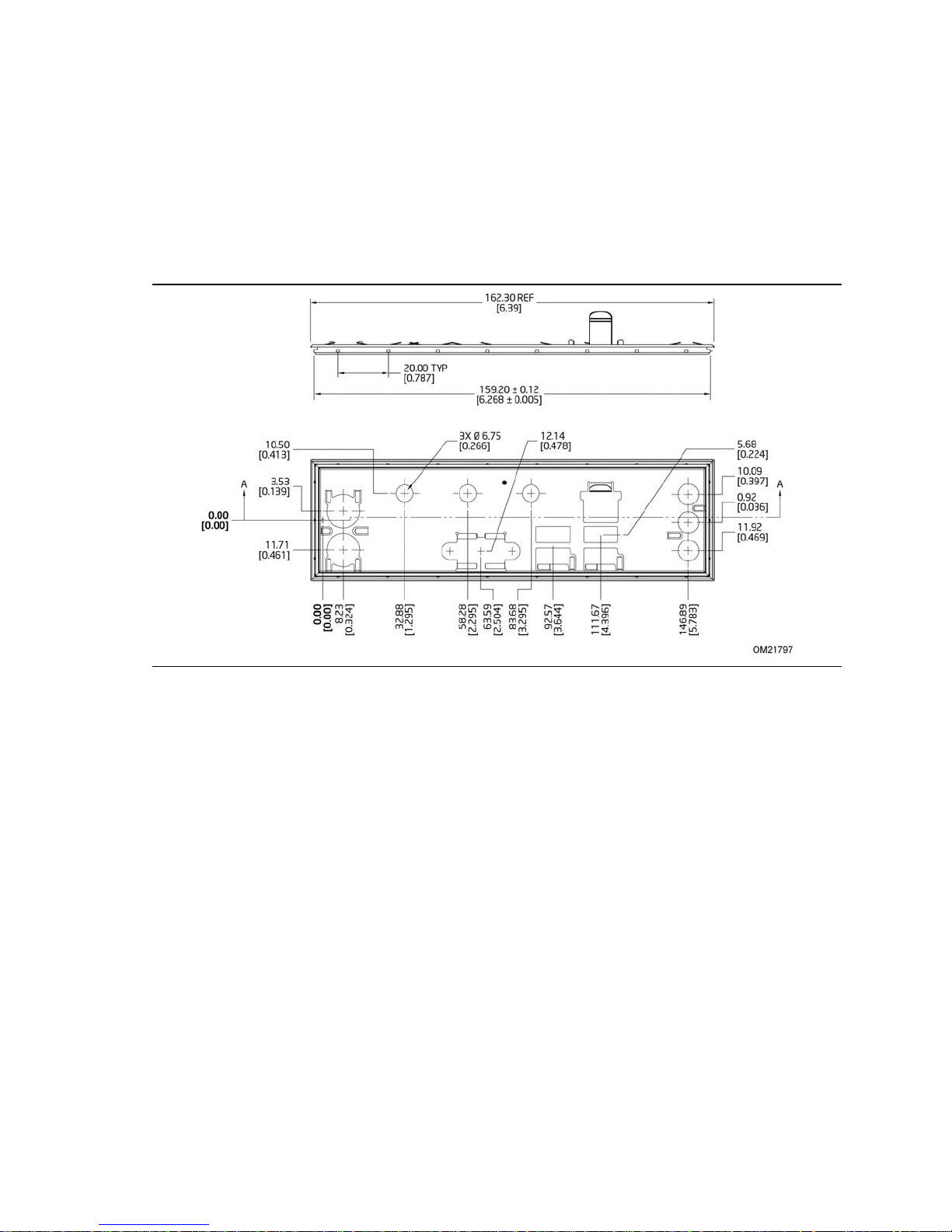
The board is designed to fit into a mini-ITX or microATX form-factor chassis. Figure 15
illustrates the mechanical form factor for the board. Dimensions are given in inches
[millimeters]. The outer dimensions are 6.7 inches by 6.7 inches [170 millimeters by
170 millimeters]. Location of the I/O connectors and mounting holes are in
compliance with the microATX specification.
56
Figure 15. Board Dimensions
Page 57

Technical Reference
2.5 Electrical Considerations
2.5.1 Fan Header Current Capability
Table 31 lists the current capability of the fan header.
Table 31. Fan Header Current Capability
Fan Header Maximum Available Current
Chassis fan 1.0 A
2.5.2 Add-in Board Considerations
The board is designed to provide 2 A (average) of +5 V current for the PCI
Conventional slot. The total +5 V current draw for the PCI Conventional expansion
slot (total load) must not exceed 2 A.
2.6 Thermal Considerations
CAUTION
A chassis with a maximum internal ambient temperature of 38 oC at the processor fan
inlet is a requirement.
CAUTION
Failure to ensure appropriate airflow may result in reduced performance of both the
processor and/or voltage regulator or, in some instances, damage to the board. For a
list of chassis that have been tested with Intel Desktop Boards please refer to the
following website:
http://developer.intel.com/design/motherbd/cooling.htm
All responsibility for determining the adequacy of any thermal or system design
remains solely with the reader. Intel makes no warranties or representations that
merely following the instructions presented in this document will result in a system
with adequate thermal performance.
CAUTION
Ensure that the ambient temperature does not exceed the board’s maximum operating
temperature. Failure to do so could cause components to exceed their maximum case
temperature and malfunction. For information about the maximum operating
temperature, see the environmental specifications in Section 2.9.
57
Page 58
Intel Desktop Board D510MO Technical Product Specification
CAUTION
Ensure that proper airflow is maintained in the processor voltage regulator circuit.
Failure to do so may result in damage to the voltage regulator circuit. The processor
voltage regulator area (shown in Figure 16) can reach a temperature of up to 85
an open chassis.
Figure 16 shows the locations of the localized high temperature zones.
o
C in
Figure 16. Localized High Temperature Zones
Table 32 provides maximum case temperatures for the board components that are
sensitive to thermal changes. The operating temperature, current load, or operating
frequency could affect case temperatures. Maximum case temperatures are important
when considering proper airflow to cool the board.
58
Item Description
A Processor voltage regulator area
B Intel Atom processor
C
Intel NM10 Express Chipset
Page 59
Technical Reference
Table 32. Thermal Considerations for Components
Component Maximum Case Temperature
Intel Atom processor 99 oC
Processor voltage regulator area 85 oC
Intel NM10 Express Chipset 113 oC
Memory DIMM 85 oC
For information about Refer to
Processor datasheets and specification updates Section 1.2, page 16
2.6.1 Passive Heatsink Design in a Passive System
Environment
This section highlights important guidelines and related thermal boundary conditions
for passive heatsink design in a passive system environment. Passive heatsink
describes a thermal solution without a fan attached. Passive system environment
describes a chassis with either a power supply fan or a built-in chassis fan.
This information should be used in conjunction with the Thermal/Mechanical
Specifications and Design Guidelines (TMSDG) published for Intel
®
Atom™ D400 and
D500 Series processors. The TMSDG contains detailed package information and
thermal mechanical specifications for the processors. The TMSDG also contains
information on how to enable a completely fanless design provided the right usage
scenario and boundary conditions are observed for optimal thermal design. While the
TMSDG has a section on thermal design for passive system environments
(pages 29-30), the information in this section can also be used to complement the
TMSDG.
2.6.1.1 Definition of Terms
Term Description
TA The measured ambient temperature locally surrounding the processor. The ambient
temperature should be measured just upstream of a passive heatsink.
TJ Processor junction temperature.
ΨJA Junction-to-ambient thermal characterization parameter (psi). A measure of thermal solution
performance using total package power. Defined as (T
Note: Heat source must be specified for Ψ measurements.
TIM Thermal Interface Material: the thermally conductive compound between the heatsink and the
processor die surface. This material fills the air gaps and voids, and enhances the transfer of the heat
from the processor die surface to the heatsink.
TDP Thermal Design Power: a power dissipation target based on worst-case applications. Thermal
solutions should be designed to dissipate the thermal design power.
TA external The measured external ambient temperature surrounding the chassis. The external ambient
temperature should be measured just upstream of the chassis inlet vent.
- TA)/TDP.
J
59
Page 60

Intel Desktop Board D510MO Technical Product Specification
2.6.1.2 Thermal Specifications Guideline
Terms Requirements
TA ≤ 50 °C
TJ ≤ 100 °C
ΨJA ≤ 3.85 °C/W
TIM Honeywell PCM45F
TDP 13 W
TA external ≤ 35 °C
2.6.1.3 Heatsink Design Guideline
Maximum heatsink size* 87 x 62 x 35.54 mm
Heatsink mass ≤ 80 grams
Retention type Spring loaded fasteners
Heatsink preload 11.3 +/- 3.6 lb
Note: Refers to the heatsink installed on the board.
2.6.1.4 Chassis Design Guideline
The pin fin heatsink design used on this board will be able to dissipate up to 13 W of
processor power in most of the passively enabled system chassis. This board is
targeted for 3-7 liters volumetric or larger, desktop/tower orientation, mini-ITX and
micro-ATX chassis with a chassis fan. The recommended fan type is an exhaust fan.
For best thermal performance, it is recommended that the chassis fan provide
reasonable airflow directly over the all the major components on the board. The pin fin
heatsink is designed to have the best thermal performance when airflow direction is
parallel to the heatsink fins.
The processor on the board will generate the highest amount of heat, leading to high
ambient temperature within the chassis. The chassis fan should be located near the
board region in order to effectively regulate airflow (see Figure 17). A chassis fan
located further away from the board region, i.e., at the optical disk drive or hard disk
driv
e region
Regardless of where the chassis fan is located, the maximum local ambient
temperature as defined by T
also provide adequate openings for airflow to pass through. The recommended freearea-ratio of chassis vents should be equal to or greater than 0.53. By using the
reference pin fin heatsink, most chassis with a chassis fan enabled should have local
ambient temperature safely below the 50 °C limit.
, will be less effective in controlling the local ambient temperature.
A should be capped at 50 °C. Chassis inlet vents should
60
Page 61

Technical Reference
Figure 17. Fan Location Guide for Cassis Selection
(Chassis Orientation is Not Restricted)
For all chassis configurations, the heatsink performance parameter, Ψ
should be less
JA
than 3.85 °C/W. The detail thermal measurement metrology is described in the
TMSDG. For chassis that fail to meet the thermal specifications guideline highlighted
above, an actively cooled heatsink solution should be used.
61
Page 62

Intel Desktop Board D510MO Technical Product Specification
2.7 Power Consumption
Power measurements were performed to determine bare minimum and likely
maximum power requirements from the board, as well as attached devices, in order to
facilitate power supply rating estimates for specific system configurations.
2.7.1 Minimum Load Configuration
Minimum load refers to the power demand placed on the power supply when using a
bare system configuration with minimal power requirement conditions. Minimum load
configuration test results are shown in Table 33. The test configuration was defined as
f
llows:
o
• 4 GB DDR2/667 MHz DIMM
• USB keyboard and mouse
• LAN linked at 1 Gb/s
• DOS booted via network (PXE); system at idle
• All on board peripherals enabled (serial, parallel, audio, …)
Table 33. Minimum Load Configuration Current and Power Results
Current Draw at 12 V Power Consumption
1.737 A 20.844 W
2.7.2 Maximum Load Configuration
Maximum load refers to the incremental power demands placed on the power supply,
augmenting the minimum load configuration into a fully-featured system that stresses
power consumption from all subsystems. Maximum load configuration test results are
shown in Table 34. The test configuration was defined as follows:
• 4 GB DDR2/667 MHz DIMM
• 14.1-inch LCD via LVDS
• SATA DVD-R/W
⎯ Load: DVD pl
• 3.5-i
• Intel Z-U130 USB Solid-State Drive (or compatible device) on the USB flash drive
• Wireless card on PCI Express Mini Card slot, connected via 802.11n protocol
• Riser card on conventional PCI slot, populated with PCI LAN card, running file
• USB keyboard and mouse
nch SATA hard disk drive, running Microsoft Windows Vista Home Basic
⎯ Load: continuous read/write benchmark
header
⎯ Load: continuous read/write benchmark
⎯ Load: continuous read/write benchmark on remote share
transfer through local network to SATA hard drive
ayback
62
Page 63

Technical Reference
• Back and front panel host-powered USB devices (other than keyboard and mouse)
⎯ Load: continuous read/write activity on external drive/peripheral
• LAN linked at 1 Gbps
⎯ Load: continuous read/write benchmark on remote share
• All on board peripherals enabled (serial, parallel, audio, …)
Table 34. Maximum Load Configuration Current and Power Results
Subsystem Current Draw at 12 V Power Consumption
Minimum Load Configuration 1.737 A 20.844 W
14.1-inch LCD via LVDS 0.532 6.384 W
SATA DVD-R/W 0.332 A 3.984 W
3.5-inch SATA hard disk drive 0.724 A 8.688 W
Intel Z-U130 USB Solid State Drive
(or compatible device)
Wireless PCI Express Mini Card 0.2 A 2.4 W
PCI cards on riser 0.131 A 1.572 W
Host-powered USB devices (other
than keyboard and mouse)
Maximum Load Configuration 3.825 A 45.9 W
0.062 A 0.744 W
0.107 A 1.284 W
2.8 Reliability
The Mean Time Between Failures (MTBF) prediction is calculated using component and
subassembly random failure rates. The calculation is based on the Bellcore Reliability
Prediction Procedure, TR-NWT-000332, Issue 4, September 1991. The MTBF
prediction is used to estimate repair rates and spare parts requirements.
The MTBF data was calculated from predicted data at 55 ºC. The Intel Desktop Board
D510MO MTBF is 248,232.584 hours.
63
Page 64

Intel Desktop Board D510MO Technical Product Specification
2.9 Environmental
Table 35 lists the environmental specifications for the board.
Table 35. Intel Desktop Board D510MO Environmental Specifications
Parameter Specification
Temperature
Non-Operating
Operating
Shock
Unpackaged 50 g trapezoidal waveform
Velocity change of 170 inches/second²
Packaged Half sine 2 millisecond
Product weight (pounds) Free fall (inches) Velocity change
<20 36 167
21-40 30 152
41-80 24 136
81-100 18 118
Vibration
Unpackaged 5 Hz to 20 Hz: 0.01 g² Hz sloping up to 0.02 g² Hz
20 Hz to 500 Hz: 0.02 g² Hz (flat)
Packaged 10 Hz to 40 Hz: 0.015 g² Hz (flat)
40 Hz to 500 Hz: 0.015 g² Hz sloping down to 0.00015 g² Hz
-20 °C to +70 °C
0 °C to +50 °C
(inches/sec²)
64
Page 65

3 Overview of BIOS Features
3.1 Introduction
The board uses an Intel BIOS that is stored in the Serial Peripheral Interface Flash
Memory (SPI Flash) and can be updated using a disk-based program. The SPI Flash
contains the BIOS Setup program, POST, the PCI auto-configuration utility, LAN
EEPROM information, and Plug and Play support.
The BIOS displays a message during POST identifying the type of BIOS and a revision
code. The initial production BIOSs are identified as MOPNV10J.86A.
The BIOS Setup program can be used to view and change the BIOS settings for the
computer. The BIOS Setup program is accessed by pressing the <F2> key after the
Power-On Self-Test (POST) memory test begins and before the operating system boot
begins. The menu bar is shown below.
Maintenance Main Advanced Security Power Boot Exit
NOTE
The maintenance menu is displayed only when the board is in configure mode.
Section 2.3 on page 54 shows how to put the board in configure mode.
65
Page 66
Intel Desktop Board D510MO Technical Product Specification
Table 36 lists the BIOS Setup program menu features.
Table 36. BIOS Setup Program Menu Bar
Maintenance Main Advanced Security Power Boot Exit
Clears
passwords and
displays
processor
information
Displays
processor
and memory
configuration
Configures
advanced
features
available
through the
chipset
Sets
passwords
and security
features
Configures
power
management
features and
power states
options
Table 37 lists the function keys available for menu screens.
Table 37. BIOS Setup Program Function Keys
Selects boot
options
Saves or
discards
changes to
Setup
program
options
BIOS Setup Program
Function Key
<←> or <→>
<↑> or <↓>
<Enter> Executes command or selects the submenu
<F9> Load the default configuration values for the current menu
<F10> Save the current values and exits the BIOS Setup program
<Esc> Exits the menu
Description
Selects a different menu screen (Moves the cursor left or right)
Selects an item (Moves the cursor up or down)
3.2 BIOS Flash Memory Organization
The Serial Peripheral Interface Flash Memory (SPI Flash) includes an 8 Mbit (1024 KB)
flash memory device.
3.3 Resource Configuration
3.3.1 PCI* Autoconfiguration
The BIOS can automatically configure PCI devices. PCI devices may be onboard or
add-in cards. Autoconfiguration lets a user insert or remove PCI cards without having
to configure the system. When a user turns on the system after adding a PCI card,
the BIOS automatically configures interrupts, the I/O space, and other system
resources. Any interrupts set to Available in Setup are considered to be available for
use by the add-in card.
66
Page 67

Overview of BIOS Features
3.4 System Management BIOS (SMBIOS)
SMBIOS is a Desktop Management Interface (DMI) compliant method for managing
computers in a managed network.
The main component of SMBIOS is the Management Information Format (MIF)
database, which contains information about the computing system and its
components. Using SMBIOS, a system administrator can obtain the system types,
capabilities, operational status, and installation dates for system components. The
MIF database defines the data and provides the method for accessing this information.
The BIOS enables applications such as third-party management software to use
SMBIOS. The BIOS stores and reports the following SMBIOS information:
• BIOS data, such as the BIOS revision level
• Fixed-system data, such as peripherals, serial numbers, and asset tags
• Resource data, such as memory size, cache size, and processor speed
• Dynamic data, such as event detection and error logging
Non-Plug and Play operating systems require an additional interface for obtaining the
SMBIOS information. The BIOS supports an SMBIOS table interface for such operating
systems. Using this support, an SMBIOS service-level application running on a
non-Plug and Play operating system can obtain the SMBIOS information. Additional
board information can be found in the BIOS under the Additional Information header
under the Main BIOS page.
67
Page 68

Intel Desktop Board D510MO Technical Product Specification
3.5 Legacy USB Support
Legacy USB support enables USB devices to be used even when the operating
system’s USB drivers are not yet available. Legacy USB support is used to access the
BIOS Setup program, and to install an operating system that supports USB. By
default, Legacy USB support is set to Enabled.
Legacy USB support operates as follows:
1. When you apply power to the computer, legacy support is disabled.
2. POST begins.
3. Legacy USB support is enabled by the BIOS allowing you to use a USB keyboard to
enter and configure the BIOS Setup program and the maintenance menu.
4. POST completes.
5. The operating system loads. While the operating system is loading, USB
keyboards and mice are recognized and may be used to configure the operating
system. (Keyboards and mice are not recognized during this period if Legacy USB
support was set to Disabled in the BIOS Setup program.)
6. After the operating system loads the USB drivers, all legacy and non-legacy USB
devices are recognized by the operating system, and Legacy USB support from the
BIOS is no longer used.
7. Additional USB legacy feature options can be accessed by using Intel Integrator
Toolkit.
To install an operating system that supports USB, verify that Legacy USB support in
the BIOS Setup program is set to Enabled and follow the operating system’s
installation instructions.
68
Page 69

Overview of BIOS Features
3.6 BIOS Updates
The BIOS can be updated using either of the following utilities, which are available on
the Intel World Wide Web site:
• Intel
• Intel
Both utilities verify that the updated BIOS matches the target system to prevent
accidentally installing an incompatible BIOS.
NOTE
Review the instructions distributed with the upgrade utility before attempting a BIOS
update.
For information about Refer to
BIOS update utilities http://downloadcenter.intel.com
®
Express BIOS Update utility, which enables automated updating while in the
Windows environment. Using this utility, the BIOS can be updated from a file on a
hard disk, a USB drive (a flash drive or a USB hard drive), or a CD-ROM, or from
the file location on the Web.
®
Flash Memory Update Utility, which requires booting from DOS. Using this
utility, the BIOS can be updated from a file on a hard disk, a USB drive (a flash
drive or a USB hard drive), or a CD-ROM.
3.6.1 BIOS Recovery
It is unlikely that anything will interrupt a BIOS update; however, if an interruption
occurs, the BIOS could be damaged. Table 38 lists the drives and media types that
can and cannot be used for BIOS recovery. The BIOS recovery media does not need
to be made bootable.
Table 38. Acceptable Drives/Media Types for BIOS Recovery
Media Type Can be used for BIOS recovery?
CD-ROM drive connected to the SATA interface Yes
USB removable drive (a USB Flash Drive, for example) Yes
USB diskette drive (with a 1.44 MB diskette) No
USB hard disk drive No
For information about Refer to
BIOS update instructions http://www.intel.com/support/motherboards/desktop/sb/
CS-022312.htm
69
Page 70

Intel Desktop Board D510MO Technical Product Specification
3.6.2 Custom Splash Screen
During POST, an Intel® splash screen is displayed by default. This splash screen can
be augmented with a custom splash screen. The Intel
available from Intel can be used to create a custom splash screen.
NOTE
If you add a custom splash screen, it will share space with the Intel branded logo.
For information about
Intel Integrator Toolkit http://developer.intel.com/design/motherbd/software/itk/
Refer to
®
Integrator’s Toolkit that is
3.7 Boot Options
In the BIOS Setup program, the user can choose to boot from optical drives, hard
drives, removable media or the network. The default setting is for the optical drive to
be the first boot device, the hard drive second, and removable media third. If
enabled, the last default boot device is the network.
3.7.1 CD-ROM Boot
Booting from CD-ROM is supported in compliance to the El Torito bootable CD-ROM
format specification. Under the Boot menu in the BIOS Setup program, ATAPI
CD-ROM is listed as a boot device. Boot devices are defined in priority order.
Accordingly, if there is not a bootable CD in the CD-ROM drive, the system will attempt
to boot from the next defined drive.
3.7.2 Network Boot
The network can be selected as a boot device. This selection allows booting from the
onboard LAN or a network add-in card with a remote boot ROM installed.
Pressing the <F12> key during POST automatically forces booting from the LAN. To
use this key during POST, the User Access Level in the BIOS Setup program's Security
menu must be set to Full.
70
Page 71

Overview of BIOS Features
3.7.3 Booting Without Attached Devices
For use in embedded applications, the BIOS has been designed so that after passing
the POST, the operating system loader is invoked even if the following devices are not
present:
• Video adapter
• Keyboard
• Mouse
3.7.4 Changing the Default Boot Device During POST
Pressing the <F10> key during POST causes a boot device menu to be displayed. This
menu displays the list of available boot devices (as set in the BIOS setup program’s
Boot Device Priority submenu). Table 39 lists the boot device menu options.
Table 39. Boot Device Menu Options
Boot Device Menu Function Keys Description
<↑> or <↓>
<Enter> Exits the menu, saves changes, and boots from the selected
<Esc> Exits the menu without saving changes
Selects a default boot device
device
71
Page 72

Intel Desktop Board D510MO Technical Product Specification
3.8 BIOS Security Features
The BIOS includes security features that restrict access to the BIOS Setup program
and who can boot the computer. A supervisor password and a user password can be
set for the BIOS Setup program and for booting the computer, with the following
restrictions:
• The supervisor password gives unrestricted access to view and change all the
Setup options in the BIOS Setup program. This is the supervisor mode.
• The user password gives restricted access to view and change Setup options in the
BIOS Setup program. This is the user mode.
• If only the supervisor password is set, pressing the <Enter> key at the password
prompt of the BIOS Setup program allows the user restricted access to Setup.
• If both the supervisor and user passwords are set, users can enter either the
supervisor password or the user password to access Setup. Users have access to
Setup respective to which password is entered.
• Setting the user password restricts who can boot the computer. The password
prompt will be displayed before the computer is booted. If only the supervisor
password is set, the computer boots without asking for a password. If both
passwords are set, the user can enter either password to boot the computer.
• For enhanced security, use different passwords for the supervisor and user
passwords.
• Valid password characters are A-Z, a-z, and 0-9. Passwords may be up to
16 characters in length.
Table 40 shows the effects of setting the supervisor password and user password.
T
is table is for reference only and is not displayed on the screen.
h
Table 40. Supervisor and User Password Functions
Password
Set
Neither Can change all
Supervisor
only
User only N/A Can change all
Supervisor
and user set
Note: If no password is set, any user can change all Setup options.
Supervisor
Mode
options
Can change all
options
Can change all
options
(Note)
User Mode
Can change all
options
Can change a
limited number
of options
options
Can change a
limited number
of options
(Note)
Setup Options
None None None
Supervisor Password Supervisor None
Enter Password
Clear User Password
Supervisor Password
Enter Password
Password
to Enter
Setup
User User
Supervisor or
user
Password
During
Boot
Supervisor or
user
72
Page 73

4 Board Status and Error Messages
4.1 BIOS Beep Codes
Whenever a recoverable error occurs during POST, the BIOS causes the board’s
speaker to beep an error message describing the problem (see Table 41).
Table 41. BIOS Beep Codes
Type Pattern Frequency
F2 Setup/F10 Boot Menu
Prompt
BIOS update in progress None
Video error On-off (1.0 second each) two times, then
Memory error On-off (1.0 second each) three times, then
Thermal trip warning Alternate high and low beeps (1.0 second each)
One 0.5 second beep when BIOS is ready to
accept keyboard input
2.5-second pause (off), entire pattern repeats
(beeps and pause) once and the BIOS will
continue to boot.
2.5-second pause (off), entire pattern repeats
(beeps and pause) until the system is powered
off.
for 8 beeps, followed by system shut down.
932 Hz
932 Hz
When no VGA option ROM is
found.
932 Hz
High beep 2000 Hz
Low beep 1500 Hz
73
Page 74

Intel Desktop Board D510MO Technical Product Specification
4.2 Front-panel Power LED Blink Codes
Whenever a recoverable error occurs during POST, the BIOS causes the board’s front
panel power LED to blink an error message describing the problem (see Table 42).
Table 42. Front-panel Power LED Blink Codes
Type Pattern Note
F2 Setup/F10 Boot Menu
Prompt
BIOS update in progress Off when the update begins, then on for
Video error On-off (1.0 second each) two times, then
Memory error On-off (1.0 second each) three times, then
Thermal trip warning Each beep will be accompanied by the following
None
0.5 seconds, then off for 0.5 seconds. The
pattern repeats until the BIOS update is
complete.
When no VGA option ROM is
2.5-second pause (off), entire pattern repeats
(blink and pause) until the system is powered
off.
2.5-second pause (off), entire pattern repeats
(blinks and pause) until the system is powered
off.
blink pattern: .25 seconds On, .25 seconds Off,
.25 seconds On, .25 seconds Off. This will result
in a total of 16 blinks.
found.
4.3 BIOS Error Messages
Whenever a recoverable error occurs during POST, the BIOS displays an error
message describing the problem. Table 43 lists the error messages and provides a
brief description of each.
Table 43. BIOS Error Messages
Error Message Explanation
CMOS Battery Low The battery may be losing power. Replace the battery soon.
CMOS Checksum Bad The CMOS checksum is incorrect. CMOS memory may have been
corrupted. Run Setup to reset values.
Memory Size Decreased Memory size has decreased since the last boot. If no memory
was removed, then memory may be bad.
No Boot Device Available System did not find a device to boot.
74
Page 75
Board Status and Error Messages
4.4 Port 80h POST Codes
During the POST, the BIOS generates diagnostic progress codes (POST codes) to I/O
port 80h. If the POST fails, execution stops and the last POST code generated is left
at port 80h. This code is useful for determining the point where an error occurred.
Displaying the POST codes requires a PCI bus add-in card, often called a POST card.
The POST card can decode the port and display the contents on a medium such as a
seven-segment display.
NOTE
The POST card must be installed in PCI bus connector 1.
The following tables provide information about the POST codes generated by the
BIOS:
• Table 44 lists the Port 80h POST code ranges
• Table 45 lists the Port 80h POST codes themselves
• Table 46 lists the Port 80h POST sequence
NOTE
In the tables listed above, all POST codes and range values are listed in hexadecimal.
Table 44. Port 80h POST Code Ranges
Range Category/Subsystem
00 – 0F Debug codes: Can be used by any PEIM/driver for debug.
10 – 1F Host Processors: 1F is an unrecoverable CPU error.
20 – 2F Memory/Chipset: 2F is no memory detected or no useful memory detected.
30 – 3F Recovery: 3F indicated recovery failure.
40 – 4F Reserved for future use.
50 – 5F I/O Busses: PCI, USB, ISA, ATA, etc. 5F is an unrecoverable error. Start with PCI.
60 – 6F Reserved for future use (for new busses).
70 – 7F Output Devices: All output consoles. 7F is an unrecoverable error.
80 – 8F Reserved for future use (new output console codes).
90 – 9F Input devices: Keyboard/Mouse. 9F is an unrecoverable error.
A0 – AF Reserved for future use (new input console codes).
B0 – BF Boot Devices: Includes fixed media and removable media. BF is an unrecoverable error.
C0 – CF Reserved for future use.
D0 – DF Boot device selection.
E0 – FF E0 – EE: Miscellaneous codes. See Table 45.
EF: boot/S3 resume failure.
F0 – FF: FF processor exception.
75
Page 76

Intel Desktop Board D510MO Technical Product Specification
Table 45. Port 80h POST Codes
POST Code Description of POST Operation
10 Power-on initialization of the host processor (Boot Strap Processor)
11 Host processor cache initialization (including APs)
12 Starting Application processor initialization
13 SMM initialization
21 Initializing a chipset component
22 Reading SPD from memory DIMMs
23 Detecting presence of memory DIMMs
24 Programming timing parameters in the memory controller and the DIMMs
25 Configuring memory
26 Optimizing memory settings
27 Initializing memory, such as ECC init
28 Testing memory
50 Enumerating PCI busses
51 Allocating resources to PCI bus
52 Hot Plug PCI controller initialization
53 – 57 Reserved for PCI Bus
58 Resetting USB bus
59 Reserved for USB
5A Resetting PATA/SATA bus and all devices
5B Reserved for ATA
5C Resetting SMBus
5D Reserved for SMBus
70 Resetting the VGA controller
71 Disabling the VGA controller
72 Enabling the VGA controller
78 Resetting the console controller
79 Disabling the console controller
7A Enabling the console controller
Host Processor
Chipset
Memory
PCI Bus
USB
ATA/ATAPI/SATA
SMBus
Local Console
Remote Console
continued
76
Page 77

Board Status and Error Messages
Table 45. Port 80h POST Codes (continued)
POST Code Description of POST Operation
90 Resetting keyboard
91 Disabling keyboard
92 Detecting presence of keyboard
93 Enabling the keyboard
94 Clearing keyboard input buffer
95 Instructing keyboard controller to run Self Test (PS/2 only)
98 Resetting mouse
99 Disabling mouse
9A Detecting presence of mouse
9B Enabling mouse
B0 Resetting fixed media
B1 Disabling fixed media
B2 Detecting presence of a fixed media (hard drive detection etc.)
B3 Enabling/configuring a fixed media
B8 Resetting removable media
B9 Disabling removable media
BA Detecting presence of a removable media (CD-ROM detection, etc.)
BC Enabling/configuring a removable media
Dy Trying boot selection y (y=0 to 15)
E0 Started dispatching PEIMs (emitted on first report of EFI_SW_PC_INIT_BEGIN
EFI_SW_PEI_PC_HANDOFF_TO_NEXT)
E2 Permanent memory found
E1, E3 Reserved for PEI/PEIMs
E4 Entered DXE phase
E5 Started dispatching drivers
E6 Started connecting drivers
Keyboard (PS/2 or USB)
Mouse (PS/2 or USB)
Fixed Media
Removable Media
BDS
PEI Core
DXE Core
continued
77
Page 78

Intel Desktop Board D510MO Technical Product Specification
Table 45. Port 80h POST Codes (continued)
POST Code Description of POST Operation
DXE Drivers
E7 Waiting for user input
E8 Checking password
E9 Entering BIOS setup
EB Calling Legacy Option ROMs
Runtime Phase/EFI OS Boot
F4 Entering Sleep state
F5 Exiting Sleep state
F8 EFI boot service ExitBootServices ( ) has been called
F9 EFI runtime service SetVirtualAddressMap ( ) has been called
FA EFI runtime service ResetSystem ( ) has been called
PEIMs/Recovery
30 Crisis Recovery has initiated per user request
31 Crisis Recovery has initiated by software (corrupt flash)
34 Loading recovery capsule
35 Handing off control to the recovery capsule
3F Unable to recover
78
Page 79

Table 46. Typical Port 80h POST Sequence
POST Code Description
21 Initializing a chipset component
22 Reading SPD from memory DIMMs
23 Detecting presence of memory DIMMs
25 Configuring memory
28 Testing memory
34 Loading recovery capsule
E4 Entered DXE phase
12 Starting application processor initialization
13 SMM initialization
50 Enumerating PCI busses
51 Allocating resourced to PCI bus
92 Detecting the presence of the keyboard
90 Resetting keyboard
94 Clearing keyboard input buffer
95 Keyboard Self Test
EB Calling Video BIOS
58 Resetting USB bus
5A Resetting PATA/SATA bus and all devices
92 Detecting the presence of the keyboard
90 Resetting keyboard
94 Clearing keyboard input buffer
5A Resetting PATA/SATA bus and all devices
28 Testing memory
90 Resetting keyboard
94 Clearing keyboard input buffer
E7 Waiting for user input
01 INT 19
00 Ready to boot
Board Status and Error Messages
79
Page 80

Intel Desktop Board D510MO Technical Product Specification
80
Page 81

5 Regulatory Compliance and Battery
Disposal Information
5.1 Regulatory Compliance
This section contains the following regulatory compliance information for Intel Desktop
Board D510MO:
• Safety standards
• European Union Declaration of Conformity statement
• Product Ecology statements
• Electromagnetic Compatibility (EMC) standards
• Product certification markings
5.1.1 Safety Standards
Intel Desktop Board D510MO complies with the safety standards stated in Table 47
when correctly installed in a compatible host system.
Table 47. Safety Standards
Standard Title
CSA/UL 60950-1, First Edition Information Technology Equipment – Safety - Part 1: General
Requirements (USA and Canada)
EN 60950-1:2006, Second
Edition
IEC 60950-1:2005, Second
Edition
Information Technology Equipment – Safety - Part 1: General
Requirements (European Union)
Information Technology Equipment – Safety - Part 1: General
Requirements (International)
81
Page 82

Intel Desktop Board D510MO Technical Product Specification
5.1.2 European Union Declaration of Conformity
Statement
We, Intel Corporation, declare under our sole responsibility that the product Intel®
Desktop Board D510MO is in conformity with all applicable essential requirements
necessary for CE marking, following the provisions of the European Council Directive
2004/108/EC (EMC Directive) and 2006/95/EC (Low Voltage Directive).
The product is properly CE marked demonstrating this conformity and is for
distribution within all member states of the EU with no restrictions.
This product follows the provisions of the European Directives 2004/108/EC and
2006/95/EC.
Čeština Tento výrobek odpovídá požadavkům evropských směrnic 2004/108/EC a
2006/95/EC.
Dansk Dette produkt er i overensstemmelse med det europæiske direktiv
2004/108/EC & 2006/95/EC.
Dutch Dit product is in navolging van de bepalingen van Europees Directief
2004/108/EC & 2006/95/EC.
Eesti Antud toode vastab Euroopa direktiivides 2004/108/EC ja 2006/95/EC
kehtestatud nõuetele.
Suomi Tämä tuote noudattaa EU-direktiivin 2004/108/EC & 2006/95/EC määräyksiä.
Français Ce produit est conforme aux exigences de la Directive Européenne
2004/108/EC & 2006/95/EC.
Deutsch Dieses Produkt entspricht den Bestimmungen der Europäischen Richtlinie
2004/108/EC & 2006/95/EC.
Ελληνικά Το παρόν προϊόν ακολουθεί τις διατάξεις των Ευρωπαϊκών Οδηγιών
2004/108/EC και 2006/95/EC.
Magyar E termék megfelel a 2004/108/EC és 2006/95/EC Európai Irányelv
előírásainak.
Icelandic Þessi vara stenst reglugerð Evrópska Efnahags Bandalagsins númer
2004/108/EC & 2006/95/EC.
Italiano Questo prodotto è conforme alla Direttiva Europea 2004/108/EC &
2006/95/EC.
Latviešu Šis produkts atbilst Eiropas Direktīvu 2004/108/EC un 2006/95/EC
noteikumiem.
Lietuvių Šis produktas atitinka Europos direktyvų 2004/108/EC ir 2006/95/EC
nuostatas.
Malti Dan il-prodott hu konformi mal-provvedimenti tad-Direttivi Ewropej
2004/108/EC u 2006/95/EC.
Norsk Dette produktet er i henhold til bestemmelsene i det europeiske direktivet
2004/108/EC & 2006/95/EC.
Polski Niniejszy produkt jest zgodny z postanowieniami Dyrektyw Unii Europejskiej
2004/108/EC i 73/23/EWG.
Portuguese Este produto cumpre com as normas da Diretiva Européia 2004/108/EC
& 2006/95/EC.
82
Page 83

Regulatory Compliance and Battery Disposal Information
Español Este producto cumple con las normas del Directivo Europeo 2004/108/EC &
2006/95/EC.
Slovensky Tento produkt je v súlade s ustanoveniami európskych direktív
2004/108/EC a 2006/95/EC.
Slovenščina Izdelek je skladen z določbami evropskih direktiv 2004/108/EC in
2006/95/EC.
Svenska Denna produkt har tillverkats i enlighet med EG-direktiv 2004/108/EC &
2006/95/EC.
Türkçe Bu ürün, Avrupa Birliği’nin 2004/108/EC ve 2006/95/EC yönergelerine uyar.
5.1.3 Product Ecology Statements
The following information is provided to address worldwide product ecology concerns
and regulations.
5.1.3.1 Disposal Considerations
This product contains the following materials that may be regulated upon disposal:
lead solder on the printed wiring board assembly.
5.1.3.2 Recycling Considerations
As part of its commitment to environmental responsibility, Intel has implemented the
Intel Product Recycling Program to allow retail consumers of Intel’s branded products
to return used products to selected locations for proper recycling.
Please consult the http://www.intel.com/intel/other/ehs/product_ecology
details of this program, including the scope of covered products, available locations,
shipping instructions, terms and conditions, etc.
中文
作为其对环境责任之承诺的部分,英特尔已实施 Intel Product Recycling Program
(英特尔产品回收计划),以允许英特尔品牌产品的零售消费者将使用过的产品退还至指定地点作
恰当的重复使用处理。
请参考http://www.intel.com/intel/other/ehs/product_ecology
了解此计划的详情,包括涉及产品之范围、回收地点、运送指导、条款和条件等。
Deutsch
Als Teil von Intels Engagement für den Umweltschutz hat das Unternehmen das Intel
Produkt-Recyclingprogramm implementiert, das Einzelhandelskunden von Intel
Markenprodukten ermöglicht, gebrauchte Produkte an ausgewählte Standorte für
ordnungsgemäßes Recycling zurückzugeben.
Details zu diesem Programm, einschließlich der darin eingeschlossenen Produkte,
verfügbaren Standorte, Versandanweisungen, Bedingungen usw., finden Sie auf der
http://www.intel.com/intel/other/ehs/product_ecology
for the
83
Page 84

Intel Desktop Board D510MO Technical Product Specification
Español
Como parte de su compromiso de responsabilidad medioambiental, Intel ha
implantado el programa de reciclaje de productos Intel, que permite que los
consumidores al detalle de los productos Intel devuelvan los productos usados en los
lugares seleccionados para su correspondiente reciclado.
Consulte la http://www.intel.com/intel/other/ehs/product_ecology
para ver los detalles
del programa, que incluye los productos que abarca, los lugares disponibles,
instrucciones de envío, términos y condiciones, etc.
Français
Dans le cadre de son engagement pour la protection de l'environnement, Intel a mis
en œuvre le programme Intel Product Recycling Program (Programme de recyclage
des produits Intel) pour permettre aux consommateurs de produits Intel de recycler
les produits usés en les retournant à des adresses spécifiées.
Visitez la page Web http://www.intel.com/intel/other/ehs/product_ecology
savoir plus sur ce programme, à savoir les produits concernés, les adresses
disponibles, les instructions d'expédition, les conditions générales, etc.
pour en
日本語
インテルでは、環境保護活動の一環として、使い終えたインテル
ブランド製品を指定の場所へ返送していただき、リサイクルを適切に行えるよう、インテル製品リサイクル
プログラムを発足させました。
対象製品、返送先、返送方法、ご利用規約など、このプログラムの詳細情報は、http://www.intel.com/in
tel/other/ehs/product_ecology (英語)をご覧ください。
Malay
Sebagai sebahagian daripada komitmennya terhadap tanggungjawab persekitaran,
Intel telah melaksanakan Program Kitar Semula Produk untuk membenarkan
pengguna-pengguna runcit produk jenama Intel memulangkan produk terguna ke
lokasi-lokasi terpilih untuk dikitarkan semula dengan betul.
Sila rujuk http://www.intel.com/intel/other/ehs/product_ecology
untuk mendapatkan
butir-butir program ini, termasuklah skop produk yang dirangkumi, lokasi-lokasi
tersedia, arahan penghantaran, terma & syarat, dsb.
Portuguese
Como parte deste compromisso com o respeito ao ambiente, a Intel implementou o
Programa de Reciclagem de Produtos para que os consumidores finais possam enviar
produtos Intel usados para locais selecionados, onde esses produtos são reciclados de
maneira adequada.
Consulte o site http://www.intel.com/intel/other/ehs/product_ecology
(em Inglês)
para obter os detalhes sobre este programa, inclusive o escopo dos produtos cobertos,
os locais disponíveis, as instruções de envio, os termos e condições, etc.
84
Page 85

Regulatory Compliance and Battery Disposal Information
Russian
В качестве части своих обязательств к окружающей среде, в Intel создана
программа утилизации продукции Intel (Product Recycling Program) для
предоставления конечным пользователям марок продукции Intel возможности
возврата используемой продукции в специализированные пункты для должной
утилизации.
Пожалуйста, обратитесь на веб-сайт
http://www.intel.com/intel/other/ehs/product_ecology
за информацией об этой
программе, принимаемых продуктах, местах приема, инструкциях об отправке,
положениях и условиях и т.д.
Türkçe
Intel, çevre sorumluluğuna bağımlılığının bir parçası olarak, perakende tüketicilerin
Intel markalı kullanılmış ürünlerini belirlenmiş merkezlere iade edip uygun şekilde geri
dönüştürmesini amaçlayan Intel Ürünleri Geri Dönüşüm Programı’nı uygulamaya
koymuştur.
Bu programın ürün kapsamı, ürün iade merkezleri, nakliye talimatları, kayıtlar ve
şartlar v.s dahil bütün ayrıntılarını ögrenmek için lütfen
http://www.intel.com/intel/other/ehs/product_ecology
Web sayfasına gidin.
5.1.3.3 Lead Free Intel Desktop Board
This Intel Desktop Board is a European Union Restriction of Hazardous Substances (EU
RoHS Directive 2002/95/EC) compliant product. EU RoHS restricts the use of six
materials. One of the six restricted materials is lead.
This Intel Desktop Board is lead free although certain discrete components used on the
board contain a small amount of lead which is necessary for component performance
and/or reliability. This Intel Desktop Board is referred to as “Lead-free second level
interconnect.” The board substrate and the solder connections from the board to the
components (second-level connections) are all lead free.
China bans the same substances and has the same limits as EU RoHS; however it
requires different product marking and controlled substance information. The required
mark shows the Environmental Friendly Usage Period (EFUP). The EFUP is defined as
the number of years for which controlled listed substances will not leak or chemically
deteriorate while in the product.
Table 48 shows the various forms of the “Lead-Free 2
appears on the board and accompanying collateral.
nd
Level Interconnect” mark as it
85
Page 86

Intel Desktop Board D510MO Technical Product Specification
Table 48. Lead-Free Board Markings
Description Mark
Lead-Free 2
This symbol is used to identify
electrical and electronic
assemblies and components in
which the lead (Pb) concentration
level in the board substrate and
the solder connections from the
board to the components (secondlevel interconnect) is not greater
than 0.1% by weight (1000 ppm).
nd
Level Interconnect:
or
or
86
Page 87

Regulatory Compliance and Battery Disposal Information
5.1.4 EMC Regulations
Intel Desktop Board D510MO complies with the EMC regulations stated in Table 49
when correctly installed in a compatible host system.
Table 49. EMC Regulations
Regulation Title
FCC 47 CFR Part 15,
Subpart B
ICES-003 Issue 4 Interference-Causing Equipment Standard, Digital Apparatus. (Canada)
EN55022:2006 Limits and methods of measurement of Radio Interference Characteristics
EN55024:1998 Information Technology Equipment – Immunity Characteristics Limits and
EN55022:2006 Australian Communications Authority, Standard for Electromagnetic
CISPR 22:2005
+A1:2005 +A2:2006
CISPR 24:1997
+A1:2001 +A2:2002
VCCI V-3/2007.04,
V-4/2007.04
KN-22, KN-24 Korean Communications Commission – Framework Act on
CNS 13438:2006 Bureau of Standards, Metrology and Inspection (Taiwan)
Title 47 of the Code of Federal Regulations, Part15, Subpart B, Radio
Frequency Devices. (USA)
of Information Technology Equipment. (European Union)
methods of measurement. (European Union)
Compatibility. (Australia and New Zealand)
Limits and methods of measurement of Radio Disturbance Characteristics of
Information Technology Equipment. (International)
Information Technology Equipment – Immunity Characteristics – Limits and
Methods of Measurement. (International)
Voluntary Control for Interference by Information Technology Equipment.
(Japan)
Telecommunications and Radio Waves Act (South Korea)
Japanese Kanji statement translation: this is a Class B product based on the standard
of the Voluntary Control Council for Interference from Information Technology
Equipment (VCCI). If this is used near a radio or television receiver in a domestic
environment, it may cause radio interference. Install and use the equipment
according to the instruction manual.
87
Page 88

Intel Desktop Board D510MO Technical Product Specification
Korean Class B statement translation: this is household equipment that is certified to
comply with EMC requirements. You may use this equipment in residential
environments and other non-residential environments.
5.1.5 Product Certification Markings (Board Level)
Intel Desktop Board D510MO has the product certification markings shown in
Table 50:
Table 50. Product Certification Markings
Description Mark
UL joint US/Canada Recognized Component mark. Includes adjacent UL file
number for Intel Desktop Boards: E210882.
FCC Declaration of Conformity logo mark for Class B equipment. Includes
Intel name and D510MO model designation.
CE mark. Declaring compliance to European Union (EU) EMC directive and
Low Voltage directive.
Australian Communications Authority (ACA) and New Zealand Radio Spectrum
Management (NZ RSM) C-tick mark. Includes adjacent Intel supplier code
number, N-232.
Japan VCCI (Voluntary Control Council for Interference) mark.
Korea Certification mark. Includes an adjacent KCC (Korean Communications
Commission) certification number:
KCC-REM-CPU-D510MO
Taiwan BSMI (Bureau of Standards, Metrology and Inspections) mark.
Includes adjacent Intel company number, D33025.
Printed wiring board manufacturer’s recognition mark. Consists of a unique
UL recognized manufacturer’s logo, along with a flammability rating (solder
side).
China RoHS/Environmentally Friendly Use Period Logo: This is an example of
the symbol used on Intel Desktop Boards and associated collateral. The color
of the mark may vary depending upon the application. The Environmental
Friendly Usage Period (EFUP) for Intel Desktop Boards has been determined
to be 10 years.
V-0
88
Page 89

Regulatory Compliance and Battery Disposal Information
5.2 Battery Disposal Information
CAUTION
Risk of explosion if the battery is replaced with an incorrect type. Batteries should be
recycled where possible. Disposal of used batteries must be in accordance with local
environmental regulations.
PRECAUTION
Risque d'explosion si la pile usagée est remplacée par une pile de type incorrect. Les
piles usagées doivent être recyclées dans la mesure du possible. La mise au rebut des
piles usagées doit respecter les réglementations locales en vigueur en matière de
protection de l'environnement.
FORHOLDSREGEL
Eksplosionsfare, hvis batteriet erstattes med et batteri af en forkert type. Batterier
bør om muligt genbruges. Bortskaffelse af brugte batterier bør foregå i
overensstemmelse med gældende miljølovgivning.
OBS!
Det kan oppstå eksplosjonsfare hvis batteriet skiftes ut med feil type. Brukte batterier
bør kastes i henhold til gjeldende miljølovgivning.
VIKTIGT!
Risk för explosion om batteriet ersätts med felaktig batterityp. Batterier ska kasseras
enligt de lokala miljövårdsbestämmelserna.
VARO
Räjähdysvaara, jos pariston tyyppi on väärä. Paristot on kierrätettävä, jos se on
mahdollista. Käytetyt paristot on hävitettävä paikallisten ympäristömääräysten
mukaisesti.
VORSICHT
Bei falschem Einsetzen einer neuen Batterie besteht Explosionsgefahr. Die Batterie
darf nur durch denselben oder einen entsprechenden, vom Hersteller empfohlenen
Batterietyp ersetzt werden. Entsorgen Sie verbrauchte Batterien den Anweisungen
des Herstellers entsprechend.
AVVERTIMENTO
Esiste il pericolo di un esplosione se la pila non viene sostituita in modo corretto.
Utilizzare solo pile uguali o di tipo equivalente a quelle consigliate dal produttore. Per
disfarsi delle pile usate, seguire le istruzioni del produttore.
89
Page 90
Intel Desktop Board D510MO Technical Product Specification
PRECAUCIÓN
Existe peligro de explosión si la pila no se cambia de forma adecuada. Utilice
solamente pilas iguales o del mismo tipo que las recomendadas por el fabricante del
equipo. Para deshacerse de las pilas usadas, siga igualmente las instrucciones del
fabricante.
WAARSCHUWING
Er bestaat ontploffingsgevaar als de batterij wordt vervangen door een onjuist type
batterij. Batterijen moeten zoveel mogelijk worden gerecycled. Houd u bij het
weggooien van gebruikte batterijen aan de plaatselijke milieuwetgeving.
ATENÇÃO
Haverá risco de explosão se a bateria for substituída por um tipo de bateria incorreto.
As baterias devem ser recicladas nos locais apropriados. A eliminação de baterias
usadas deve ser feita de acordo com as regulamentações ambientais da região.
AŚCIAROŽZNAŚĆ
Існуе рызыка выбуху, калі заменены акумулятар неправільнага тыпу.
Акумулятары павінны, па магчымасці, перепрацоўвацца. Пазбаўляцца ад старых
акумулятараў патрэбна згодна з мясцовым заканадаўствам па экалогіі.
UPOZORNÌNÍ
V případě výměny baterie za nesprávný druh může dojít k výbuchu. Je-li to možné,
baterie by měly být recyklovány. Baterie je třeba zlikvidovat v souladu s místními
předpisy o životním prostředí.
Προσοχή
Υπάρχει κίνδυνος για έκρηξη σε περίπτωση που η μπαταρία αντικατασταθεί από μία
λανθασμένου τύπου. Οι μπαταρίες θα πρέπει να ανακυκλώνονται όταν κάτι τέτοιο είναι
δυνατό. Η απόρριψη των χρησιμοποιημένων μπαταριών πρέπει να γίνεται σύμφωνα με
τους κατά τόπο περιβαλλοντικούς κανονισμούς.
VIGYAZAT
Ha a telepet nem a megfelelő típusú telepre cseréli, az felrobbanhat. A telepeket
lehetőség szerint újra kell hasznosítani. A használt telepeket a helyi környezetvédelmi
előírásoknak megfelelően kell kiselejtezni.
90
Page 91
Regulatory Compliance and Battery Disposal Information
AWAS
Risiko letupan wujud jika bateri digantikan dengan jenis yang tidak betul. Bateri
sepatutnya dikitar semula jika boleh. Pelupusan bateri terpakai mestilah mematuhi
peraturan alam sekitar tempatan.
OSTRZEŻENIE
Istnieje niebezpieczeństwo wybuchu w przypadku zastosowania niewłaściwego typu
baterii. Zużyte baterie należy w miarę możliwości utylizować zgodnie z odpowiednimi
przepisami ochrony środowiska.
PRECAUŢIE
Risc de explozie, dacă bateria este înlocuită cu un tip de baterie necorespunzător.
Bateriile trebuie reciclate, dacă este posibil. Depozitarea bateriilor uzate trebuie să
respecte reglementările locale privind protecţia mediului.
ВНИМАНИЕ
При использовании батареи несоответствующего типа существует риск ее взрыва.
Батареи должны быть утилизированы по возможности. Утилизация батарей
должна проводится по правилам, соответствующим местным требованиям.
UPOZORNENIE
Ak batériu vymeníte za nesprávny typ, hrozí nebezpečenstvo jej výbuchu.
Batérie by sa mali podľa možnosti vždy recyklovať. Likvidácia použitých batérií sa musí
vykonávať v súlade s miestnymi predpismi na ochranu životného prostredia.
POZOR
Zamenjava baterije z baterijo drugačnega tipa lahko povzroči eksplozijo.
Če je mogoče, baterije reciklirajte. Rabljene baterije zavrzite v skladu z lokalnimi
okoljevarstvenimi predpisi.
.
UYARI
Yanlış türde pil takıldığında patlama riski vardır. Piller mümkün olduğunda geri
dönüştürülmelidir. Kullanılmış piller, yerel çevre yasalarına uygun olarak atılmalıdır.
OСТОРОГА
Використовуйте батареї правильного типу, інакше існуватиме ризик вибуху.
Якщо можливо, використані батареї слід утилізувати. Утилізація використаних
батарей має бути виконана згідно місцевих норм, що регулюють охорону довкілля.
91
Page 92

Intel Desktop Board D510MO Technical Product Specification
92
 Loading...