

Page 1

BL440ZX Motherboard
Technical Product Specification
December 1998
Order Number 726092-001
The BL440ZX motherboard may contain design defects or errors known as errata that may cause the product to deviate from published specifications. Current characterized errata
are documented in the BL440ZX Motherboard Specification Update.
Page 2

Revision History
Revision Revision History Date
-001 First release of the BL440ZX Motherboard Technical Product
Specification.
This product specification applies only to standard BL440ZX motherboards with BIOS identifier
4B4LZ0XA.86A.000X.P0X.
Changes to this specification will be published in the BL440ZX Motherboard Specification Update
before being incorporated into a revision of this document.
December 1998
Information in this doc ument is provided in connec tion with Intel product s. No license, express or impl ied, by est oppel or
otherwise, to any intellectual property rights is granted by this document. Except as provided in Intel’s Terms and
Conditions of Sale for such products, Intel ass umes no liability whatsoever, and Intel disc laims any express or implied
warranty, relating to sale and/or use of Intel products including liability or warranties relating to fitness for a particular
purpose, merchantability, or infringement of any patent, copyright or other intellectual propert y right Intel products are not
designed, intended or authorized for use in any medical, life saving, or life sustaining applications or for any other
application in which the failure of the Intel product could create a situation where personal injury or death may occur.
Intel retains the right to make changes to specifications and product descriptions at any time, without notice.
The BL440ZX motherboard may contain design defects or errors known as errata whi ch may cause the produc t to deviate
from published specifications. Current characterized errata are available on request.
Contact your local Intel sales office or your distributor to obtain the latest specifications before placing your product order.
Copies of documents whic h have an ordering number and are referenc ed in this docum ent, or other Intel lit erature, may be
obtained from:
Intel Corporation
P.O. Box 5937
Denver, CO 80217-9808
or call in North America 1-800-548-4725, Europe 44-0-1793-431-155, France 44-0-1793-421-777,
Germany 44-0-1793-421-333, other Countries 708-296-9333.
†
Third party brands and names are the property of their respective owners.
Copyright Intel Corporation, 1998.
Page 3

Preface
This Technical Product Specification (TPS) specifies the board layout, components, connectors,
power and environmental requirements, and BIOS for the BL440ZX motherboard. It describes the
standard motherboard product and available manufacturing options.
Intended Audience
The TPS is intended to provide detailed, technical information about the motherboard and its
components to the vendors, system integrators, and other engineers and technicians who need this
level of information. It is specifically not intended for general audiences.
What This Document Contains
Chapter Description
1 A description of the hardware used on this board
2 A map of the resources of the board
3 The features supported by the BIOS Setup program
4 The contents of the BIOS Setup program’s menus and submenus
5 A description of the BIOS error messages, beep codes, and Power On Self Tests
(POST) codes
6 A list of where to find information about specifications supported by the
motherboard
Typographical Conventions
This section contains information about the conventions used in this specification. Not all of these
symbols and abbreviations appear in all specifications of this type.
Notes, Cautions, and Warnings
NOTE
✏
Notes call attention to important information.
CAUTION
Cautions are included to help you avoid damaging hardware or losing data.
iii
Page 4

BL440ZX Motherboard Technical Product Specification
WARNING
Warnings indicate conditions that, if not observed, can cause personal injury.
Other Common Notation
‡
# Used after a signal name to identify an active-low signal (such as USBP0#).
(NxnX) When used in the description of a component, N indicates component type, xn are the relative
KB Kilobyte (1024 bytes).
Kbit Kilobit (1024 bits).
MB Megabyte (1,048,576 bytes).
Mbit Megabit (1,048,576 bits).
GB Gigabyte (1,073,741,824 bytes).
xxh An address or data value ending with a lowercase h indicates a hexadecimal value.
x.x V Volts. Voltages are DC unless otherwise specified.
†
Indicates a feature that is implemented—at least in part—on a riser card.
coordinates of its location on the motherboard, and X is the instance of the particular part at that
general location. For example, J5J1 is a connector, located at 5J. It is the first connector in the
5J area.
This symbol is used to indicate third-party brands and names that are the property of their
respective owners.
iv
Page 5

Contents
1 Motherboard Description
1.1 Overview ................................................................................................................... 10
1.2 Microprocessor.......................................................................................................... 13
1.3 Main Memory............................................................................................................. 13
1.4 Chipset......................................................................................................................15
1.4.1 Intel
1.4.2 Intel
1.5 I/O Interface Controller .............................................................................................. 18
1.5.1 Serial Port ................................................................................................... 18
1.5.2 Parallel Port................................................................................................. 19
1.5.3 Diskette Drive Controller.............................................................................. 19
1.5.4 PS/2 Keyboard and Mouse Interface........................................................... 19
1.6 Audio Subsystem....................................................................................................... 20
1.6.1 Creative Sound Blaster AudioPCI 64V AC ’97 v1.03 Digital Controller........ 20
1.6.2 Crystal CS4297 AC ’97 v1.03 Analog Codec............................................... 20
1.6.3 Audio Connectors........................................................................................ 20
1.6.4 Audio Drivers and Utilities ........................................................................... 21
1.7 ATI RAGE PRO TURBO 2X AGP Graphics Controller .............................................. 21
1.8 LAN Subsystem......................................................................................................... 21
1.8.1 Intel
1.8.2 LAN Subsystem Software............................................................................ 22
1.8.3 RJ-45 LAN Connector LEDs........................................................................ 22
1.9 Wake on LAN Technology......................................................................................... 22
1.10 Wake on Ring / Resume on Ring Technologies......................................................... 23
1.10.1 Wake on Ring Technology .......................................................................... 23
1.10.2 Resume on Ring Technology...................................................................... 23
1.11 Hardware Monitor Subsystem.................................................................................... 23
1.12 Fan Speed Control .................................................................................................... 23
1.12.1 Fan Header................................................................................................. 24
1.12.2 Fan Control Signal to the Riser Card........................................................... 24
1.12.3 System Management Support..................................................................... 24
1.13 Motherboard Connectors........................................................................................... 25
1.13.1 Back Panel I/O Connectors......................................................................... 26
1.13.2 Processor Fan Connector............................................................................ 29
1.13.3 NLX Card Edge Connector.......................................................................... 29
1.14 Jumper Blocks........................................................................................................... 39
1.14.1 Microphone Routing Jumper Block.............................................................. 40
1.14.2 BIOS Setup Configuration Jumper Block..................................................... 40
1.15 Mechanical Considerations........................................................................................ 41
1.15.1 Form Factor................................................................................................. 41
1.15.2 I/O Shield.................................................................................................... 42
82443ZX PCI/AGP Controller............................................................ 15
82371EB PCI ISA IDE Xcelerator...................................................... 16
82559 LAN Controller........................................................................ 21
v
Page 6

BL440ZX Motherboard Technical Product Specification
1.16 Electrical Considerations........................................................................................... 43
1.16.1 Power Consumption.................................................................................... 43
1.16.2 Power Supply Considerations...................................................................... 44
1.17 Thermal Considerations............................................................................................. 45
1.18 Environmental Specifications..................................................................................... 47
1.19 Reliability................................................................................................................... 47
1.20 Regulatory Compliance ............................................................................................. 48
2 Motherboard Resources
2.1 Memory Map ............................................................................................................. 49
2.2 DMA Channels .......................................................................................................... 50
2.3 I/O Map ..................................................................................................................... 50
2.4 PCI Configuration Space Map ................................................................................... 52
2.5 Interrupts...................................................................................................................53
2.6 PCI Interrupt Routing Map......................................................................................... 54
3 Overview of BIOS Features
3.1 Introduction................................................................................................................ 55
3.2 BIOS Flash Memory Organization............................................................................. 56
3.3 Resource Configuration............................................................................................. 56
3.3.1 Plug and Play: PCI Autoconfiguration......................................................... 56
3.3.2 ISA Plug and Play ....................................................................................... 56
3.3.3 PCI IDE Support.......................................................................................... 57
3.4 System Management BIOS (SMBIOS)...................................................................... 57
3.5 Power Management .................................................................................................. 58
3.5.1 APM............................................................................................................ 58
3.5.2 ACPI............................................................................................................ 58
3.6 BIOS Upgrades ......................................................................................................... 60
3.6.1 Language Support....................................................................................... 61
3.6.2 OEM Logo or Scan Area............................................................................. 61
3.7 Recovering BIOS Data .............................................................................................. 61
3.8 Boot Options.............................................................................................................. 62
3.8.1 CD-ROM and Network Boot........................................................................ 62
3.8.2 Booting Without Attached Devices .............................................................. 62
3.8.3 Default Settings After Battery and Power Failure ........................................ 62
3.9 USB Legacy Support................................................................................................. 63
3.10 BIOS Security Features............................................................................................. 64
4 BIOS Setup Program
4.1 Introduction................................................................................................................ 65
4.2 Maintenance Menu.................................................................................................... 66
4.3 Main Menu................................................................................................................. 67
4.4 Advanced Menu......................................................................................................... 68
4.4.1 Boot Setting Configuration Submenu .......................................................... 68
4.4.2 Peripheral Configuration Submenu.............................................................. 69
4.4.3 IDE Configuration........................................................................................ 70
4.4.4 IDE Configuration Submenus...................................................................... 71
4.4.5 Diskette Configuration Submenu................................................................. 72
vi
Page 7

4.4.6 Event Log Configuration.............................................................................. 72
4.4.7 Video Configuration Submenu..................................................................... 72
4.4.8 Resource Configuration Submenu............................................................... 73
4.5 Security Menu............................................................................................................ 73
4.6 Power Menu.............................................................................................................. 74
4.7 Boot Menu................................................................................................................. 74
4.8 Exit Menu .................................................................................................................. 75
5 Error Messages and Beep Codes
5.1 BIOS Error Messages................................................................................................ 77
5.2 Port 80h POST Codes............................................................................................... 79
5.3 Bus Initialization Checkpoints.................................................................................... 83
5.4 BIOS Beep Codes..................................................................................................... 84
6 Specifications and Customer Support
6.1 Online Support........................................................................................................... 85
6.2 Specifications ............................................................................................................ 85
Figures
1. Motherboard Components......................................................................................... 12
2. Motherboard Connectors........................................................................................... 25
3. Locations of the Jumper Blocks................................................................................. 39
4. Motherboard Dimensions........................................................................................... 41
5. Back Panel I/O Shield Dimensions ............................................................................ 42
6. Thermally-sensitive Components............................................................................... 46
Contents
Tables
1. Processors Supported by the Motherboard ............................................................... 13
2. RJ-45 LAN Connector LEDs...................................................................................... 22
3. Fan Speed Control under APM Operating System .................................................... 24
4. Fan Speed Control under ACPI Operating System.................................................... 24
5. Video Connector (J1K1) ............................................................................................ 26
6. Parallel Port Connector (J2K1).................................................................................. 27
7. Serial Port Connector (J3K1)..................................................................................... 27
8. RJ-45 LAN connector (J6K2)..................................................................................... 27
9. PS/2 Keyboard/Mouse Connectors (J5K1, J6K1)...................................................... 28
10. USB Connectors (J6K2) ............................................................................................ 28
11. Audio Line Out Connector (J7K1)............................................................................. 28
12. Audio Mic In Connector (J8K1)................................................................................. 28
13. Processor Fan Connector (J4D1).............................................................................. 29
14. Available PCI Bus Masters........................................................................................ 29
15. PCI Segment, NLX Card Edge Connector................................................................. 31
16. ISA Segment, NLX Card Edge Connector................................................................. 32
17. IDE, Floppy, and Front Panel Section; NLX Card Edge Connector............................ 34
18. Supplemental Section, NLX Card Edge Connector.................................................... 37
19. Microphone Routing Jumper (J8K2) .......................................................................... 40
20. BIOS Setup Configuration Jumper Settings............................................................... 40
21. Power Usage............................................................................................................. 43
vii
Page 8

BL440ZX Motherboard Technical Product Specification
22. DC Voltage Tolerances.............................................................................................. 44
23. Thermal Considerations for Components .................................................................. 45
24. Environmental Specifications..................................................................................... 47
25. Safety Regulations .................................................................................................... 48
26. EMC Regulations....................................................................................................... 48
27. System Memory Map................................................................................................. 49
28. DMA Channels .......................................................................................................... 50
29. I/O Map ..................................................................................................................... 50
30. PCI Configuration Space Map ................................................................................... 52
31. Interrupts...................................................................................................................53
32. PCI Interrupt Routing Map......................................................................................... 54
33. Flash Memory Organization....................................................................................... 56
34. Effects of Pressing the Power Switch ........................................................................ 59
35. Power States and Targeted System Power ............................................................... 59
36. Wake-up Devices and Events.................................................................................... 60
37. Supervisor and User Password Functions................................................................. 64
38. Setup Menu Bar......................................................................................................... 65
39. Setup Function Keys.................................................................................................. 66
40. Maintenance Menu.................................................................................................... 66
41. Main Menu................................................................................................................. 67
42. Advanced Menu......................................................................................................... 68
43. Boot Setting Configuration Submenu......................................................................... 68
44. Peripheral Configuration Submenu............................................................................ 69
45. IDE Device Configuration .......................................................................................... 70
46. IDE Configuration Submenus .................................................................................... 71
47. Diskette Configuration Submenu............................................................................... 72
48. Event Log Configuration Submenu............................................................................ 72
49. Video Configuration Submenu................................................................................... 72
50. Resource Configuration Submenu............................................................................. 73
51. Security Menu............................................................................................................ 73
52. Power Menu.............................................................................................................. 74
53. Boot Menu................................................................................................................. 74
54. Exit Menu .................................................................................................................. 75
55. BIOS Error Messages................................................................................................ 77
56. Uncompressed INIT Code Checkpoints..................................................................... 79
57. Boot Block Recovery Code Checkpoints ................................................................... 79
58. Runtime Code Uncompressed in F000 Shadow RAM ............................................... 80
59. Beep Codes............................................................................................................... 84
60. Compliance with Specifications ................................................................................. 85
viii
Page 9

1 Motherboard Description
What This Chapter Contains
1.1 Overview ................................................................................................................... 10
1.2 Microprocessor.......................................................................................................... 13
1.3 Main Memory............................................................................................................. 13
1.4 Chipset......................................................................................................................15
1.5 I/O Interface Controller .............................................................................................. 18
1.6 Audio Subsystem....................................................................................................... 20
1.7 ATI RAGE PRO TURBO 2X AGP Graphics Controller .............................................. 21
1.8 LAN Subsystem......................................................................................................... 21
1.9 Wake on LAN Technology......................................................................................... 22
1.10 Wake on Ring / Resume on Ring Technologies......................................................... 23
1.11 Hardware Monitor Subsystem.................................................................................... 23
1.12 Fan Speed Control .................................................................................................... 23
1.13 Motherboard Connectors........................................................................................... 25
1.14 Jumper Blocks........................................................................................................... 39
1.15 Mechanical Considerations........................................................................................ 41
1.16 Electrical Considerations........................................................................................... 43
1.17 Thermal Considerations............................................................................................. 45
1.18 Environmental Specifications..................................................................................... 47
1.19 Reliability................................................................................................................... 47
1.20 Regulatory Compliance ............................................................................................. 48
9
Page 10

BL440ZX Motherboard Technical Product Specification
1.1 Overview
The BL440ZX motherboard is a versatile platform that offers a wide variety of features. Some of
the features are implemented—at least in part—on the riser card. Throughout this manual, the
symbol is used to indicate such a feature. Because there is no standard riser card, no detailed
description of an implementation can be given. See Section 6.2 to obtain NLX riser card design
information.
The BL440ZX motherboard’s features are summarized below.
Form Factor NLX (10.0 inches by 8.25 inches)
Processor
Chipset
Memory
I/O Control
Peripheral Interfaces
LAN Subsystem
Audio Subsystem
Graphics Subsystem
Expansion Capabilities
Offboard Chassis
Intrusion Detection
BIOS
• 370-contact processor pin grid array PGA370S socket
• Support for the Intel
• 128 KB of integrated L2 cache
Intel® 82440ZX AGPset (on the 66-Mhz host bus), consisting of:
• Intel
• Intel
• Two 168-contact DIMM sockets
• Support for up to 256 MB of 66-MHz, non-ECC, synchronous DRAM
• Support for serial presence detect (SPD) and non-SPD DIMMs
SMSC FDC37M807 I/O controller
• One serial port
• Two USB ports
• One parallel port
• PS/2
• PS/2 mouse
• Intel® 82559 10/100 Mbps PCI LAN controller
• RJ-45 LAN connector
Integrated PCI audio, consisting of:
• Creative Sound Blaster
• Crystal CS4297 AC ’97 v1.03 analog codec
• Integrated ATI RAGE PRO TURBO
• 8 MB SDRAM
Riser dependent
Support for chassis intrusion detection if available on the riser card (see also,
Manufacturing Options)
• Intel/AMI BIOS stored in Intel® E28F200B5 2 Mbit flash memory
• Support for SMBIOS, ACPI, APM, Management Level 3.0, and Plug and
®
82443ZX PCI/AGP controller (PAC)
®
82371EB PCI/ISA IDE Xcelerator (PIIX4E)
(SDRAM)
†
keyboard
ES1373 AC ’97 v1.03 digital controller
Play (see Section 6.2 for specification compliance levels)
®
Celeron™ processor on the 66-MHz host bus
†
AudioPCI† 64V audio using the Ensoniq
†
2X AGP controller
‡
10
Page 11

Motherboard Description
Not all of the following manufacturing options are available in all marketing channels. Please
contact your Intel representative to determine what manufacturing options are available to you.
Manufacturing Options
Front Panel USB
Onboard Chassis
Intrusion Detection
‡
One of the two USB channels routed to the riser card
Photo sensor on the motherboard
11
Page 12

BL440ZX Motherboard Technical Product Specification
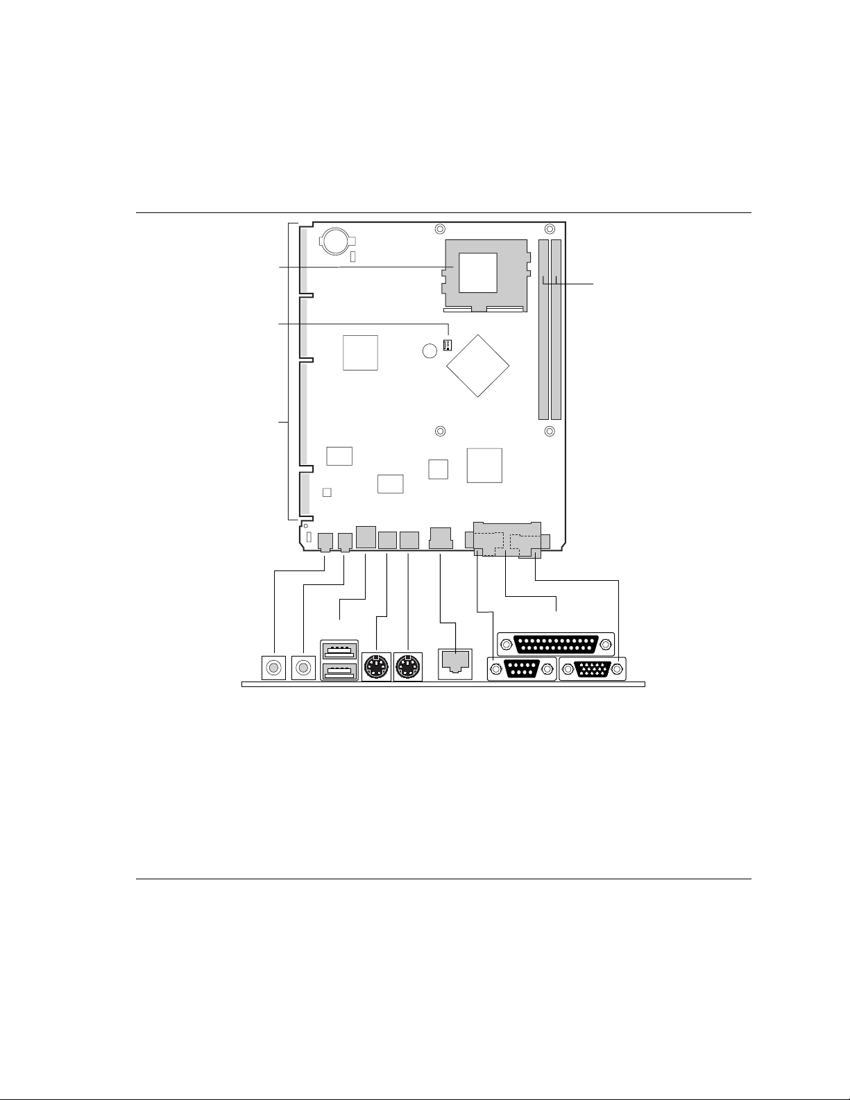
Figure 1 shows the major components of the BL440ZX motherboard.
A
Q
P
O
B
C
D
E
N
F
G
M
J
L
A Back panel I/O connectors J BIOS Setup configuration jumper
B Microphone routing jumper K Hardware monitor component
C Crystal CS4297 audio codec L PGA370S processor socket
D Creative Sound Blaster AudioPCI 64V audio
controller
EFNLX card edge connector
Piezoelectric speaker
G Intel 82371EB PIIX4E P Intel 82559 LAN controller
H Processor fan connector Q SMSC FDC37M807 I/O controller
I Battery
MNDIMM sockets
O ATI RAGE PRO TURBO 2X AGP graphics
K
®
Intel
82443ZX PAC
controller
I
H
OM07455
12
Figure 1. Motherboard Components
Page 13

Motherboard Description
1.2 Microprocessor
The motherboard supports a socketed Celeron processor. The processor’s VID pins automatically
program the voltage regulator on the motherboard to the required processor voltage. The processor
connects to the motherboard through the 370-pin PGA370S socket.
The motherboard supports the processors listed in Table 1.
Table 1. Processors Supported by the Motherboard
Processor Speed Host Bus Frequency Cache Size
300A MHz
333 MHz
366 MHz
66 MHz
66 MHz
66 MHz
128 KB
128 KB
128 KB
All supported onboard memory can be cached.
1.3 Main Memory
The motherboard has two dual inline memory module (DIMM) sockets. SDRAM can be installed
in one or both sockets. The motherboard also supports both serial presence detect (SPD) and nonSPD data structures.
2
Using the SPD data structure programmed into an E
PROM on the DIMM, the BIOS can
determine the SDRAM size and speed. Using the non-SPD data structure, the BIOS will
dynamically determine SDRAM size and speed. Minimum memory size is 16 MB; maximum
memory size is 256 MB. Memory size and speed can vary between sockets. The BIOS can
support an SPD SDRAM DIMM in one socket and a non-SPD SDRAM DIMM in the other.
CAUTION
BIOS recovery cannot be done using non-SPD DIMMs. SPD data structure is required for the
recovery process.
The motherboard supports the following memory features:
• 168-pin DIMMs with gold-plated contacts
• 66-MHz or 100-MHz unbuffered SDRAM on the 66-MHz host bus
• Non-ECC (64-bit) memory
• 3.3 V memory only
13
Page 14

BL440ZX Motherboard Technical Product Specification
The motherboard supports single- or double-sided DIMMs in the following sizes:
DIMM
Capacity
16 MB 2 Mbit X 64 16 Mbit 1 M X 16 8
16 MB 2 Mbit X 64 16 Mbit 2 M X 8 8
16 MB 2 Mbit X 64 64 Mbit 2 M X 32 2
32 MB 4 Mbit X 64 16 Mbit 2 M X 8 16*
32 MB 4 Mbit X 64 64 Mbit 2 M X 32 4
32 MB 4 Mbit X 64 64 Mbit 4 M X 16 4
64 MB 8 Mbit X 64 64 Mbit 4 M X 16 8
64 MB 8 Mbit X 64 64 Mbit 8 M X 8 8
128 MB 16 Mbit X 64 64 Mbit 8 M X 8 16*
* If the number of SDRAMs is greater than nine, the DIMM will be double-sided.
NOTE
✏
DIMM
Organization
SDRAM
Density
SDRAM
Organization
Number of
SDRAMs
All memory components and DIMMs used with the BL440ZX motherboard must comply with the
PC SDRAM Unbuffered DIMM Specification. You can access this document through the Internet
at: http://www.intel.com/design/pcisets/memory/
See Section 6.2 for information about this SDRAM DIMM specification.
14
Page 15

Motherboard Description
1.4 Chipset
The Intel 82440ZX AGPset includes a Host-PCI bridge integrated with both an optimized DRAM
controller and an Accelerated Graphics Port (AGP) interface. The I/O subsystem of the 82440ZX
is based on the PIIX4E, which is a highly integrated PCI-ISA/IDE Accelerator Bridge.
1.4.1 Intel 82443ZX PCI/AGP Controller
The Intel 82443ZX PCI/AGP controller (PAC) provides bus-control signals, address paths, and
data paths for transfers between the processor’s host bus, PCI bus, the AGP, and main memory.
The PAC features:
• Processor interface control
Support for 66-MHz processor host bus
32-bit addressing
Desktop optimized GTL+ compliant host bus interface
• Integrated DRAM controller, with support for
+3.3 V only DIMM DRAM configurations
Up to two double-sided DIMMs
100-MHz or 66-MHz SDRAM on the 66-MHz host bus
DIMM serial presence detect via SMBus interface
16- and 64-Mbit devices with 2 KB, 4 KB, and 8 KB page sizes
x 4, x 8, x 16, and x 32 DRAM widths
Symmetrical and asymmetrical DRAM addressing
• AGP interface
Complies with the AGP specification (see Section 6.2 for specification information)
Support for a 2X AGP device
Synchronous coupling to the host bus frequency
• PCI bus interface
Complies with the PCI specification Rev. 2.1, +5 V 33-MHz interface (see Section 6.2 for
specification information)
Asynchronous coupling to the host-bus frequency
PCI parity generation support
Data streaming support from PCI-to-DRAM
Support for four PCI bus masters in addition to the host and PCI-to-ISA I/O bridge
Support for concurrent host, AGP, and PCI transactions to main memory
• Data buffering
DRAM write buffer with read-around-write capability
Dedicated host-to-DRAM, PCI0-to-DRAM, and PCI1/AGP-to-DRAM read buffers
AGP dedicated inbound/outbound FIFOs, used for temporary data storage
• ACPI and APM power management compliance
• SMBus support for desktop management functions
• Support for system management mode (SMM)
15
Page 16

BL440ZX Motherboard Technical Product Specification
1.4.2 Intel 82371EB PCI ISA IDE Xcelerator
The Intel 82371EB PCI ISA IDE Xcelerator (PIIX4E) is a multifunction PCI device implementing
the PCI-to-ISA bridge, PCI IDE functionality, Universal Serial Bus (USB) host/hub functionality,
and enhanced power management. The PIIX4E features:
• Multifunction PCI-to-ISA bridge
Support for the PCI bus at 33 MHz
PCI specification compliance (see Section 6.2 for specification information)
Full ISA bus support
• USB controller
Two USB ports (see Section 6.2 for specification information)
Legacy support for USB keyboard and mouse
Support for the Universal Host Controller Interface (UHCI) Design Guide, revision 1.1,
interface
• Integrated dual-channel enhanced IDE interface
Support for up to four IDE devices
PIO Mode 4 transfers up to 16 MB/sec
Support for Ultra DMA/33 synchronous DMA mode transfers up to 33 MB/sec
Bus master mode with an 8 x 32-bit buffer for bus master PCI IDE burst transfers
• Enhanced DMA controller
Two 8237-based DMA controllers
Support for PCI DMA with three PC/PCI channels and distributed DMA protocols
• Interrupt controller based on 82C59
Support for 15 interrupts
Programmable edge/level sensitivity
• Power management logic
Sleep/resume logic
Support for Wake on LAN
Support for ACPI (see Section 6.2 for specification information)
• Real-Time Clock
256-byte battery-backed CMOS SRAM
Date alarm
• 16-bit counters/timers based on 82C54
†
technology
16
Page 17

Motherboard Description
1.4.2.1 Universal Serial Bus (USB)
The motherboard has two USB ports; one USB peripheral can be connected to each port. For more
than two USB devices, an external hub can be connected to either port. The motherboard provides
the two USB ports on the back panel. For riser cards with front panel USB port support, a
motherboard manufacturing option is available that provides one USB port on the back panel and
the other USB channel routed to the riser card.
The motherboard fully supports the universal host controller interface (UHCI) and uses UHCIcompatible software drivers. See Section 6.2 for information about the USB specification.
USB features include:
• Self-identifying peripherals that can be plugged in while the computer is running
• Automatic mapping of function to driver and configuration
• Support for isochronous and asynchronous transfer types over the same set of wires
• Support for up to 127 physical devices
• Guaranteed bandwidth and low latencies appropriate for telephony, audio, and other
applications
• Error-handling and fault-recovery mechanisms built into the protocol
NOTE
✏
Computer systems that have an unshielded cable attached to a USB port may not meet FCC
Class B requirements, even if no device or a low-speed USB device is attached to the cable. Use
shielded cable that meets the requirements for full-speed devices.
1.4.2.2 IDE Support
The motherboard has two independent bus-mastering IDE interfaces. These interfaces support:
• ATAPI devices (such as CD-ROM drives)
• ATA devices using the transfer modes listed in Table 46
The BIOS supports logical block addressing (LBA) and extended cylinder head sector (ECHS)
translation modes. The drive reports the transfer rate and translation mode to the BIOS.
The motherboard supports laser servo (LS-120) diskette technology through its IDE interfaces.
The LS-120 drive can be configured as a boot device by setting the BIOS Setup program’s Boot
Device Menu (see Section 4.7) to one of the following:
• ARMD-FDD (ATAPI Removable Media Device - Floppy Disk Drive)
• ARMD-HDD (ATAPI Removable Media Device - Hard Disk Drive)
1.4.2.3 Real-Time Clock, CMOS SRAM, and Battery
The real-time clock is compatible with DS1287 and MC146818 components. The clock provides a
time-of-day clock and a multicentury calendar with alarm features and century rollover. The realtime clock supports 256 bytes of battery-backed CMOS SRAM in two banks that are reserved for
BIOS use.
The time, date, and CMOS values can be specified in the Setup program. The CMOS values can
be returned to their defaults by using the Setup program.
17
Page 18

BL440ZX Motherboard Technical Product Specification
NOTE
✏
The recommended method of accessing the date in systems with Intel motherboards is from the
Real-Time Clock (RTC) via the BIOS. The BIOS on Intel motherboards contains a century
checking and maintenance feature that checks the least two significant digits of the year stored in
the RTC during each BIOS request (INT 1Ah). During this check, the BIOS reads the date and, if
less than 80 (i.e., 1980 is the first year supported by the PC), updates the century byte to 20. This
feature enables operating systems and applications using the BIOS date/time services to reliably
manipulate the year as a four-digit value.
For more information on proper date access in systems with Intel motherboards, please see
http://support.intel.com/support/year2000/motherboard.htm
A coin-cell battery powers the real-time clock and CMOS memory. When the computer is not
plugged into a wall socket, the battery has an estimated life of three years. When the computer is
plugged in, the 3.3 V standby current extends the life of the battery. The clock is accurate to ± 13
minutes/year at 25 ºC with 3.3 V applied.
1.5 I/O Interface Controller
The motherboard uses the SMSC FDC37M807 I/O controller, which features:
• Support for one diskette drive
• ISA Plug-and-Play compatible register set
• One serial port
• FIFO support on both serial port and diskette drive interfaces
• One parallel port with ECP and EPP support
• PS/2-style mouse and keyboard interfaces
• PCI PME interface to PIIX4E
• Intelligent automatic power management of devices when certain conditions are met. Support
includes:
Shadowed write-only registers for ACPI compliance
Programmable wake-up event interface
The Setup program provides configuration options for the I/O controller.
1.5.1 Serial Port
The motherboard has one serial port. The 9-pin D-sub connector for serial port A is located on the
back panel. The serial port has an NS16C550-compatible UART that supports data transfers at
speeds up to 115.2 Kbits/sec with BIOS support.
18
Page 19

Motherboard Description
1.5.2 Parallel Port
The connector for the multimode bidirectional parallel port is a 25-pin D-Sub connector located on
the back panel of the motherboard. In the Setup program, there are four options for parallel port
operation:
• Output only (standard mode).
• Bidirectional (PS/2 compatible).
• Bidirectional Enhanced Parallel Port (EPP). A driver from the peripheral manufacturer is
required for operation. See Section 6.2 for EPP compliance.
• Bidirectional high-speed Extended Capabilities Port (ECP).
1.5.3 Diskette Drive Controller
The I/O controller is software-compatible with the 82077 diskette drive controller and supports a
†
single diskette drive in either PC-AT
interface can be configured for the following diskette drive capacities and sizes:
• 360 KB, 5.25-inch
• 1.2 MB, 5.25-inch
• 720 KB, 3.5-inch
• 1.2 MB, 3.5-inch (driver required)
• 1.25/1.44 MB, 3.5-inch
• 2.88 MB, 3.5-inch
or PS/2 mode. In the Setup program, the diskette drive
1.5.4 PS/2 Keyboard and Mouse Interface
PS/2 keyboard and mouse connectors are located on the back panel of the motherboard. The +5 V
†
lines to these connectors are protected with a PolySwitch
reestablishes the connection after an overcurrent condition is removed.
NOTE
✏
The mouse and keyboard can be plugged into either PS/2 connector. Power to the computer
should be turned off before a keyboard or mouse is connected or disconnected.
The keyboard controller contains code that provides the traditional keyboard and mouse control
functions and also supports Power On/Reset password protection. A Power On/Reset password
can be specified in the BIOS Setup program.
circuit that, like a self-healing fuse,
19
Page 20

BL440ZX Motherboard Technical Product Specification
1.6 Audio Subsystem
The BL440ZX motherboard includes an Audio Codec ’97-compatible (AC ’97) audio subsystem
consisting of these devices:
• Creative Labs Sound Blaster AudioPCI 64V AC ’97 digital controller
• Crystal CS4297 AC ’97 V1.03 analog codec
The audio subsystem features include (with riser card dependencies noted):
• Split digital/analog architecture for improved S/N (signal-to-noise) ratio: > 80 dB—measured
at line out and from any analog input including line in, CD-ROM, auxiliary line in, and video
(stereo audio from a video source)
• Ensoniq 3D positional audio support
• Power management support for APM, ACPI, and PCI (see Section for 6.2 for specification
compliance levels)
• Audio inputs:
Two analog line-level stereo inputs for connection from CD-ROM audio (from the riser
card)
One mono analog line-level input for telephony (speakerphone input from the riser card)
One mono microphone input (A motherboard jumper routes the signal from the back panel
or the riser card. See Table 19 for jumpering information.)
• Audio outputs:
Stereo line-level output (shareable between the back panel and the riser card)
Mono output for speakerphone (from the riser card)
1.6.1 Creative Sound Blaster AudioPCI 64V AC ’97 v1.03 Digital
Controller
Creative Sound Blaster AudioPCI 64V, using the Ensoniq ES1373 digital controller, provides the
following features:
• PCI compliance (see Section for 6.2 for specification compliance level)
• PCI bus master for PCI audio
• 64-voice hardware wavetable
†
• Aureal A3D
• Ensoniq 3D positional audio and Microsoft DirectSound
API, Sound Blaster Pro†, Roland MPU-401 MIDI, joystick compatibility
†
3D support
1.6.2 Crystal CS4297 AC ’97 v1.03 Analog Codec
The Crystal CS4297 AC ’97 v1.03 analog codec provides the following features:
• 18 bit stereo full-duplex codec
• Fixed 48 kHz sampling rate
1.6.3 Audio Connectors
See Section 1.13.1 for the location and pinouts of the motherboard audio connectors. Other audio
connectors may be supported on the riser card.
20
Page 21

Motherboard Description
1.6.4 Audio Drivers and Utilities
Audio software and utilities are available from Intel’s World Wide Web site (see Section 6.1).
1.7 ATI RAGE PRO TURBO 2X AGP Graphics Controller
The ATI RAGE PRO TURBO 2X AGP graphics controller provides the following features:
• Comprehensive AGP support, including 2X (133 MHz) fully pipelined operation and sideband
support
• Full bus mastering support
• Triple 8-bit palette DAC with gamma correction. Pixel rates up to 230 MHz
• DDC1 and DDC2B+ for Plug and Play monitors
• Game acceleration including support for Microsoft’s DirectDraw†: double buffering, virtual
sprites, transparent blit, masked blit, and context chaining
• 4 KB on-chip texture cache
†
• Direct3D
The motherboard provides 8 MB of SDRAM graphics memory.
texture lighting
See Intel’s World Wide Web site (see Section 6.1) for graphics drivers.
1.8 LAN Subsystem
The Intel 82559 Fast Ethernet Wired for Management (WfM) PCI LAN subsystem provides both
10Base-T and 100Base-TX connectivity. Features include:
• 32-bit direct bus mastering on the PCI bus
• Shared memory structure in the host memory that copies data directly to/from host memory
• 10Base-T and 100Base-TX capability using a single RJ-45 connector with connection and
activity status LEDs
• IEEE 802.3µ Auto-Negotiation for the fastest available connection
• Jumperless configuration; the LAN subsystem is completely software-configurable
See Section 6.2 for Wired for Management specification information.
1.8.1 Intel 82559 LAN Controller
The integrated Intel 82559 LAN controller features include:
• 3.3 V operation
• CSMA/CD Protocol Engine
• PCI bus interface (see Section 6.2 for PCI specification information)
• DMA engine for movement of commands, status, and network data across the PCI bus
21
Page 22

BL440ZX Motherboard Technical Product Specification
• Integrated physical layer interface, including:
Complete functionality necessary for the 10Base-T and 100Base-TX network interfaces;
when in 10 Mbit/sec mode, the interface drives the cable directly
A complete set of Media Independent Interface (MII) management registers for control
and status reporting
802.3µ Auto-Negotiation for automatically establishing the best operating mode when
connected to other 10Base-T or 100Base-TX devices, whether half- or full-duplex capable
• Integrated power management features, including:
Support for APM
Support for Wake on LAN technology
1.8.2 LAN Subsystem Software
The Intel 82559 Fast Ethernet WfM PCI LAN software and drivers are available from Intel’s
World Wide Web site (see Section 6.1).
1.8.3 RJ-45 LAN Connector LEDs
Two LEDs are built into the RJ-45 LAN connector. They indicate the following LAN conditions.
Table 2. RJ-45 LAN Connector LEDs
LED Color LED State Indicates
Green Off 10 Mbit/sec speed is selected.
On 100 Mbit/sec speed is selected.
Yellow Off LAN link is not established.
On (steady state) LAN link is established.
On (brighter and pulsing) The computer is communicating with another computer on
the LAN.
1.9 Wake on LAN Technology
Wake on LAN technology enables remote wake-up of the computer through a network. This
feature can be implemented in one of two ways: using the onboard Intel 82559 LAN controller or,
if the riser card has a Wake on LAN technology connector, using a PCI add-in network interface
card (NIC) with remote wake-up capabilities. If using a NIC, the remote wake-up connector on the
NIC must be connected to the riser card Wake on LAN technology connector.
The onboard or NIC LAN controller monitors network traffic at the MII; upon detecting a Magic
†
Packet
CAUTION
Operation of this motherboard requires a power supply providing at least 720 mA of current on
the +5 VSB line. Failure to provide adequate standby current when implementing Wake on LAN
technology can damage the power supply.
, the controller asserts a wake-up signal that powers up the computer.
22
Page 23

Motherboard Description
1.10 Wake on Ring / Resume on Ring Technologies
This section describes two technologies that enable telephony devices to access the computer when
it is in a power-managed state.
1.10.1 Wake on Ring Technology
The operation of Wake on Ring can be summarized as follows:
• Powers up the computer from the APM Soft-Off mode
• Requires two calls to access the computer:
First call powers up the computer
Second call enables access
• Implements incoming call differently for external as opposed to internal modems:
For external modems, motherboard hardware monitors the ring indicate (RI) input of the
serial port
For internal modems, a cable must be routed from the modem to the Wake on Ring
connector
1.10.2 Resume on Ring Technology
The operation of Resume on Ring can be summarized as follows:
• Resumes operation from the APM sleep mode or the ACPI S1 state
• Requires only one call to access the computer
1.11 Hardware Monitor Subsystem
The hardware monitor subsystem provides low-cost instrumentation capabilities. The features of
the hardware monitor subsystem include:
• An integrated ambient temperature sensor
• Fan speed sensors (see Figure 2 for the location of fan connector on the motherboard)
• Power supply voltage monitoring to detect levels above or below acceptable values
• Support for chassis intrusion detection using an optional onboard photo sensor or a two-pin
connector on the riser card
When suggested ratings for temperature, fan speed, or voltage are exceeded, an interrupt is
activated. The hardware monitor component connects to the SMBus.
1.12 Fan Speed Control
The motherboard includes two independent circuits for controlling various system cooling fans:
one is on the motherboard and the other is routed to the riser card.
23
Page 24

BL440ZX Motherboard Technical Product Specification
1.12.1 Fan Header
The processor fan header (J4D1) on the motherboard is intended to drive a processor-mounted fan
either full-speed or off, depending on the operating state of the system. The fan speed is monitored
®
by the hardware monitor subsystem and can be read by applications such as Intel
LANDesk
Client Manager (LDCM) using the System Management BIOS (SMBIOS) described in
Section 3.4.
1.12.2 Fan Control Signal to the Riser Card
The NLX specification defines the fan control (FAN_CTL) signal as a means to control the speeds
of fans connected to an NLX riser card or power supply. The BL440ZX motherboard is capable of
driving FAN_CTL at different output levels, depending on the operating state of the system.
Initially, two levels are defined for high and low fan speed operation. Based on the cooling needs
and capabilities of a given system platform, the system OEM can redefine these output levels to
achieve a better balance of acoustic and thermal performance. Applications such as LDCM can
access the SMBIOS to redefine the FAN_CTL output levels.
1.12.3 System Management Support
®
While the system is running an APM operating system, the BIOS controls both fan circuits, as
shown in Table 3. With an ACPI operating system, the voltage to both circuits depends on the
system state, as shown in Table 4.
Table 3. Fan Speed Control under APM Operating System
Processor Fan Voltage
APM System States
Full On / Standby +12 V (default) OEM-definable “high speed”
Suspend 0 V (default) OEM-definable “low speed”
Table 4. Fan Speed Control under ACPI Operating System
ACPI Sleep States
S0 +12 V +12 V
S1 * *
S2 No support No support
S3 No support No support
S4 No support No support
S5 0 V 0 V
(connector J4D1, pin 2)
Processor Fan Voltage
(connector J4D1, pin 2)
FAN_CTL Signal to Riser Card
(current limit = 50 mA)
(default = +12 V)
(default = +8 V)
FAN_CTL Signal to Riser Card
(current limit = 50 mA)
* Controlled by the operating system.
24
Page 25
1.13 Motherboard Connectors
Figure 2 show the location of the motherboard connectors.
N
M
L
Motherboard Description
A
1
H
GF B
I
JK
A DIMM sockets H USB Port 1
B Video I USB Port 0
C Parallel port J Audio Line Out
D Serial port K Audio Mic In
E RJ-45 LAN L NLX riser card edge
F PS/2 keyboard/mouse M Processor fan
G PS/2 keyboard/mouse N PGA370S processor socket
E D
C
OM08436
Figure 2. Motherboard Connectors
25
Page 26

BL440ZX Motherboard Technical Product Specification
CAUTION
Only the back panel connectors of this motherboard have overcurrent protection. The internal
motherboard connectors do not have overcurrent protection; they should connect only to devices
inside the computer chassis, such as fans and internal peripherals. Do not use these connectors
for powering devices external to the computer chassis. A fault in the load presented by the
external devices could cause damage to the computer, the interconnecting cable, and the external
devices themselves.
1.13.1 Back Panel I/O Connectors
Table 5. Video Connector (J1K1)
Pin Signal Name
1 Red
2 Green
3 Blue
4 No connect
5 Ground
6 Ground
7 Ground
8 Ground
9 Fused VCC
10 Ground
11 No connect
12 MONID1
13 HSYNC
14 VSYNC
15 MONID2
26
Page 27

Table 6. Parallel Port Connector (J2K1)
Pin Signal Name Pin Signal Name
1 Strobe# 14 Auto Feed#
2 Data bit 0 15 Fault#
3 Data bit 1 16 INIT#
4 Data bit 2 17 SLCT IN#
5 Data bit 3 18 Ground
6 Data bit 4 19 Ground
7 Data bit 5 20 Ground
8 Data bit 6 21 Ground
9 Data bit 7 22 Ground
10 ACK# 23 Ground
11 Busy 24 Ground
12 Error 25 Ground
13 Select
Motherboard Description
Table 7. Serial Port Connector (J3K1)
Pin Signal Name
1 DCD
2 Serial In#
3 Serial Out#
4 DTR
5 Ground
6 DSR
7 RTS
8 CTS
9RI
Table 8. RJ-45 LAN connector (J6K2)
Pin Signal Name
1 Tx+
2 Tx3 Rx+
4 Floating plane termination
5 Floating plane termination
6 Rx7 Floating plane termination
8 Floating plane termination
27
Page 28

BL440ZX Motherboard Technical Product Specification
Table 9. PS/2 Keyboard/Mouse Connectors
(J5K1, J6K1)
Pin Signal Name
1 Data
2 No connect
3 Ground
4 +5 V (fused)
5 Clock
6 No connect
Table 10. USB Connectors (J6K2)
Pin Signal Name
1 +5 V (fused)
2 USBP0#
3 USBP0
4 Ground
5 +5 V (fused)
6 USBP1#
7 USBP1
8 Ground
Table 11. Audio Line Out Connector (J7K1)
Pin Signal Name
Sleeve Ground
Tip Audio Left Out
Ring Audio Right Out
Table 12. Audio Mic In Connector (J8K1)
Pin Signal Name
Sleeve Ground
Tip Mono In
Ring Electret Bias Voltage
28
Page 29

Motherboard Description
1.13.2 Processor Fan Connector
Table 13. Processor Fan Connector (J4D1)
Pin Signal Name
1 Ground
2 Fan Voltage (see Tables 3 and 4)
3 Tachometer
1.13.3 NLX Card Edge Connector
The motherboard card edge connector for the riser card consists of gold finger contacts in two
sections: a primary 340-position (2 x 170) section and a supplemental 26-position (2 x 13) section.
In accordance with the NLX specification, the motherboard card edge connector provides the
following:
• PCI signals (The motherboard supports at least two request/grant signal pairs on the NLX
connector. See Table 14.)
• ISA signals
• Two IDE channels
• An interface for one diskette drive
• Audio signals: CD Input, Audio Line Out, Audio Mic In, Modem Mic, and Modem Speaker
• Miscellaneous front panel signals
• Power connection for the motherboard
Tables 15, 16, and 17 specify the pinout of the primary connector; Table 18 specifies the pinout of
the supplemental connector.
All edge connector pins are defined in the NLX Motherboard Specification (see Section 6.2 for
specification information).
The 82443ZX PAC supports a total of four PCI bus masters. Table 14 tells how many PCI bus
masters are available for the NLX riser based on the board configuration.
Table 14. Available PCI Bus Masters
This is the maximum
number of PCI bus
masters available to
If the motherboard has these PCI bus masters…
PIIX4E only (no onboard PCI LAN or PCI audio) 4 REQ# / GNT# 0, 1, 2, and 3
PIIX4E + onboard PCI LAN
PIIX4E + onboard PCI audio
PIIX4E + onboard PCI LAN + onboard PCI audio
an NLX riser card…
3 REQ# / GNT# 0, 1, and 2
3 REQ# / GNT# 0, 1, and 2
2 REQ# / GNT# 0 and 1
These are the REQ# / GNT#
signal pairs routed to the
NLX riser card…
29
Page 30

BL440ZX Motherboard Technical Product Specification
NOTE
✏
If the NLX riser has more PCI bus connectors than there are REQ# / GNT# signal pairs routed to
the riser, not all of the PCI bus connectors on the riser will support bus mastering. For example, if
the motherboard has only REQ# / GNT# signal pairs 0 and 1 routed to the NLX riser connector
and the riser has three PCI bus connectors, the connector tied to REQ# / GNT# signal pair 2 will
not support bus mastering.
30
Page 31

Motherboard Description
Table 15. PCI Segment, NLX Card Edge Connector
Pin Signal Name Type I/O Termination Pin Signal Name Type I/O Termination
A1 -12V PWR N/A N/A B1 (PCSPKR_RT) *
A2 REQ4# PCI I RIS B2 +12V PWR N/A N/A
A3 +12V PWR N/A N/A B3 (PCSPKR_LFT) *
A4 GNT4# PCI O RIS B4 +12V PWR N/A N/A
A5 3.3VDC PWR N/A N/A B5 PCICLK0 PCI O MB
A6 PCIINT3# PCI I RIS B6 GND PWR N/A N/A
A7 3.3VDC PWR N/A N/A B7 PCICLK1 PCI O MB
A8 PCIINT0# PCI I RIS B8 SER_IRQ MISC I/O MB
A9 PCIINT1# PCI I RIS B9 PCIINT2# PCI I RIS
A10 PCICLK2 PCI O MB B10 3.3VDC PWR N/A N/A
A11 3.3VDC PWR N/A N/A B11 PCICLK3 PCI O MB
A12 PCI_RST# PCI O MB B12 GND PWR N/A N/A
A13 GNT0# PCI O RIS B13 GNT3# PCI O RIS
A14 PCICLK4 PCI O MB B14 3.3VDC PWR N/A N/A
A15 GND PWR N/A N/A B15 GNT2# PCI O RIS
A16 GNT1# PCI O RIS B16 AD[31] PCI I/O RIS
A17 3.3VDC PWR N/A N/A B17 REQ0# PCI I RIS
A18 REQ2# PCI I RIS B18 GND PWR N/A N/A
A19 REQ3# PCI I RIS B19 AD[29] PCI I/O RIS
A20 AD[30] PCI I/O RIS B20 AD[28] PCI I/O RIS
A21 GND PWR N/A N/A B21 AD[26] PCI I/O RIS
A22 AD[25] PCI I/O RIS B22 3.3VDC PWR N/A N/A
A23 REQ1# PCI I RIS B23 AD[24] PCI I/O RIS
A24 AD[27] PCI I/O RIS B24 C/BE[3]# PCI I/O RIS
A25 3.3VDC PWR N/A N/A B25 AD[22] PCI I/O RIS
A26 AD[23] PCI I/O RIS B26 GND PWR N/A N/A
A27 AD[20] PCI I/O RIS B27 AD[21] PCI I/O RIS
A28 AD[18] PCI I/O RIS B28 AD[19] PCI I/O RIS
A29 GND PWR N/A N/A B29 AD[16] PCI I/O RIS
Signal Name Column Definition:
* = Not implemented on motherboard
I/O Column Definitions Relative to Motherboard:
O = Output from motherboard to riser card
I = Input from riser card to motherboard
Termination Column Definitions:
MB = Termination/pullup/pulldown/debounce is on motherboard
RIS = Termination/pullup/pulldown is on riser card
N/A = Not on motherboard or riser card
continued
31
Page 32

BL440ZX Motherboard Technical Product Specification
Table 15. PCI Segment, NLX Card Edge Connector (continued)
Pin Signal Name Type I/O Termination Pin Signal Name Type I/O Termination
A30 AD[17] PCI I/O RIS B30 3.3VDC PWR N/A N/A
A31 IRDY# PCI I/O RIS B31 C/BE[2]# PCI I/O RIS
A32 DEVSEL# PCI I/O RIS B32 FRAME# PCI I/O RIS
A33 3.3VDC PWR N/A N/A B33 TRDY# PCI I/O RIS
A34 STOP# PCI I/O RIS B34 GND PWR N/A N/A
A35 PERR# PCI I/O RIS B35 (SDONE) *
A36 SERR# PCI I/O RIS B36 LOCK# PCI I/O RIS
A37 GND PWR N/A N/A B37 (SBO#) *
A38 C/BE[1]# PCI I/O RIS B38 3.3VDC PWR N/A N/A
A39 AD[13] PCI‘ I/O RIS B39 AD[15] PCI I/O RIS
A40 AD[10] PCI I/O RIS B40 PAR PCI I/O RIS
A41 GND PWR N/A N/A B41 AD[14] PCI I/O RIS
A42 C/BE[0]# PCI I/O RIS B42 GND PWR N/A N/A
A43 AD[00] PCI I/O RIS B43 AD[11] PCI I/O RIS
A44 AD[06] PCI I/O RIS B44 AD[12] PCI I/O RIS
A45 3.3VDC PWR N/A N/A B45 AD[09] PCI I/O RIS
A46 AD[05] PCI I/O RIS B46 3.3VDC PWR N/A N/A
A47 AD[01] PCI I/O RIS B47 AD[08] PCI I/O RIS
A48 AD[03] PCI I/O RIS B48 AD[07] PCI I/O RIS
A49 GND PWR N/A N/A B49 AD[04] PCI I/O RIS
A50 AD[02] PCI I/O RIS B50 GND PWR N/A N/A
A51 5VDC PWR N/A N/A B51 PCI_PM# PCI I/O MB
Signal Name Column Definition:
* = Not implemented on motherboard
I/O Column Definitions Relative to Motherboard:
O = Output from motherboard to riser card
I = Input from riser card to motherboard
Termination Column Definitions:
MB = Termination/pullup/pulldown/debounce is on motherboard
RIS = Termination/pullup/pulldown is on riser card
N/A = Not on motherboard or riser card
Table 16. ISA Segment, NLX Card Edge Connector
Pin Signal Name Type I/O Termination Pin Signal Name Type I/O Termination
A52 RSTDRV ISA O MB B52 5VDC PWR N/A N/A
A53 IOCHK# ISA I MB B53 IRQ9 ISA O MB
A54 SD[6] ISA I/O MB B54 DRQ2 ISA I MB
A55 SD[7] ISA I/O MB B55 SD[3] ISA I/O MB
A56 SD[4] ISA I/O MB B56 0WS# ISA I MB
A57 5VDC PWR N/A N/A B57 SD[1] ISA I/O MB
A58 SD[2] ISA I/O MB B58 AEN ISA O MB
A59 SD[5] ISA I/O MB B59 IOCHRDY ISA I MB
continued
32
Page 33

Motherboard Description
Table 16. ISA Segment, NLX Card Edge Connector (continued)
Pin Signal Name Type I/O Termination Pin Signal Name Type I/O Termination
A60 SD[0] ISA I/O MB B60 SA[18] ISA I/O MB
A61 SMEMW# ISA O MB B61 SMEMR# ISA O MB
A62 SA[19] ISA I/O MB B62 SA[16] ISA I/O MB
A63 IOW# ISA I/O MB B63 IOR# ISA I/O MB
A64 SA[17] ISA I/O MB B64 DRQ3 ISA I MB
A65 GND PWR N/A N/A B65 SA[15] ISA I/O MB
A66 DACK#3 ISA O MB B66 GND PWR N/A N/A
A67 SA[14] ISA I/O MB B67 SA[13] ISA I/O MB
A68 DACK1# ISA O MB B68 5VDC PWR N/A N/A
A69 DRQ1 ISA I MB B69 REFRESH# ISA I/O MB
A70 SA[12] ISA I/O MB B70 SA[11] ISA I/O MB
A71 SYSCLK ISA O MB B71 SA[10] ISA I/O MB
A72 SA[9] ISA I/O MB B72 IRQ7 ISA I MB
A73 5VDC PWR N/A N/A B73 IRQ6 ISA I MB
A74 IRQ5 ISA I MB B74 SA[8] ISA I/O MB
A75 SA[7] ISA I/O MB B75 SA[6] ISA I/O MB
A76 IRQ3 ISA I MB B76 DACK2# ISA O MB
A77 IRQ4 ISA I MB B77 SA[4] ISA I/O MB
A78 SA[5] ISA I/O MB B78 GND PWR N/A N/A
A79 TC ISA O MB B79 SA[3] ISA I/O MB
A80 BALE ISA O MB B80 SA[2] ISA I/O MB
A81 GND PWR N/A N/A B81 SA[1] ISA I/O MB
A82 OSC ISA O MB B82 SA[0] ISA I/O MB
A83 IOCS16# ISA I MB B83 SBHE# ISA I/O MB
A84 MEMCS16# ISA I MB B84 LA[23] ISA I/O MB
A85 IRQ11 ISA I MB B85 LA[22] ISA I/O MB
A86 IRQ10 ISA I MB B86 LA[21] ISA I/O MB
A87 IRQ15 ISA I MB B87 LA[20] ISA I/O MB
A88 IRQ12 ISA I MB B88 LA[19] ISA I/O MB
A89 GND PWR N/A N/A B89 LA[18] ISA I/O MB
I/O Column Definitions Relative to Motherboard:
O = Output from motherboard to riser card
I = Input from riser card to motherboard
Termination Column Definitions:
MB = Termination/pullup/pulldown/debounce is on motherboard
RIS = Termination/pullup/pulldown is on riser card
N/A = Not on motherboard or riser card
continued
33
Page 34

BL440ZX Motherboard Technical Product Specification
Table 16. ISA Segment, NLX Card Edge Connector (continued)
Pin Signal Name Type I/O Termination Pin Signal Name Type I/O Termination
A90 IRQ14 ISA I MB B90 LA[17] ISA I/O MB
A91 DRQ0 ISA I MB B91 DACK0# ISA O MB
A92 MEMR# ISA I/O MB B92 DACK5# ISA O MB
A93 MEMW# ISA I/O MB B93 SD[8] ISA I/O MB
A94 SD[9] ISA I/O MB B94 DACK6# ISA O MB
A95 DRQ5 ISA I MB B95 SD[10] ISA I/O MB
A96 DRQ6 ISA I MB B96 5VDC PWR N/A N/A
A97 5VDC PWR N/A N/A B97 SD[11] ISA I/O MB
A98 SD[12] ISA I/O MB B98 DRQ7 ISA I MB
A99 DACK7# ISA O MB B99 SD[13] ISA I/O MB
A100 SD[14] ISA I/O MB B100 SD[15] ISA I/O MB
A101 MASTER# ISA I MB B101 GND PWR N/A N/A
Table 17. IDE, Floppy, and Front Panel Section; NLX Card Edge Connector
Pin Signal Name Type I/O Termination Pin Signal Name Type I/O Termination
A102 IDEA_DD8 IDE I/O MB B102 GND PWR N/A N/A
A103 IDEA_RESET# IDE O MB B103 IDEA_DD7 IDE I/O MB
A104 IDEA_DD9 IDE I/O MB B104 IDEA_DD6 IDE I/O MB
A105 5VDC PWR N/A N/A B105 IDEA_DD5 IDE I/O MB
A106 IDEA_DD4 IDE I/O MB B106 IDEA_DD11 IDE I/O MB
A107 IDEA_DD10 IDE I/O MB B107 IDEA_DD12 IDE I/O MB
A108 IDEA_DD3 IDE I/O MB B108 GND PWR N/A N/A
A109 IDEA_DD13 IDE I/O MB B109 IDEA_DD14 IDE I/O MB
A110 IDEA_DD1 IDE I/O MB B110 IDEA_DD2 IDE I/O MB
A111 GND PWR N/A N/A B111 IDEA_DD0 IDE I/O MB
A112 IDEA_DIOW# IDE O MB B112 IDEA_DD15 IDE I/O MB
A113 IDEA_DMARQ IDE I MB B113 IDEA_DIOR# IDE O MB
continued
I/O Column Definitions Relative to Motherboard:
O = Output from motherboard to riser card
I = Input from riser card to motherboard
Termination Column Definitions:
MB = Termination/pullup/pulldown/debounce is on motherboard
RIS = Termination/pullup/pulldown is on riser card
N/A = Not on motherboard or riser card
34
Page 35

Motherboard Description
Table 17. IDE, Floppy, and Front Panel Section; NLX Card Edge Connector (continued)
Pin Signal Name Type I/O Termination Pin Signal Name Type I/O Termination
A114 IDEA_IORDY IDE I MB B114 IDEA_CSEL IDE O MB
A115 IDEA_DMACK# IDE O MB B115 IDEA_INTRQ IDE I MB
A116 RESERVED RES N/A N/A B116 5VDC PWR N/A N/A
A117 IDEA_DA2 IDE O MB B117 IDEA_DA1 IDE O MB
A118 IDEA_CS0# IDE O MB B118 IDEA_DA0 IDE O MB
A119 5VDC PWR N/A N/A B119 IDEA_CS1# IDE O MB
A120 (IDEA_DASP#) * B120 IDEB_DD8 IDE I/O MB
A121 IDEB_RESET# IDE O MB B121 IDEB_DD7 IDE I/O MB
A122 IDEB_DD9 IDE I/O MB B122 GND PWR N/A N/A
A123 IDEB_DD6 IDE I/O MB B123 IDEB_DD10 IDE I/O MB
A124 IDEB_DD5 IDE I/O MB B124 5VDC PWR N/A N/A
A125 IDEB_DD11 IDE I/O MB B125 IDEB_DD4 IDE I/O MB
A126 IDEB_DD12 IDE I/O MB B126 IDEB_DD3 IDE I/O MB
A127 GND PWR N/A N/A B127 IDEB_DD13 IDE I/O MB
A128 IDEB_DD2 IDE I/O MB B128 IDEB_DD14 IDE I/O MB
A129 IDEB_DD15 IDE I/O MB B129 IDEB_DD1 IDE I/O MB
A130 IDEB_DIOW# IDE I/O MB B130 IDEB_DD0 IDE I/O MB
A131 IDEB_DMARQ IDE I MB B131 IDEB_DIOR# IDE O MB
A132 IDEB_IORDY IDE I MB B132 IDEB_CSEL IDE O MB
A133 GND PWR N/A N/A B133 IDEB_INTRQ IDE I MB
A134 IDEB_DMACK# IDE O MB B134 IDEB_DA1 IDE O MB
A135 RESERVED RES N/A N/A B135 IDEB_DA2 IDE O MB
A136 IDEB_DA0 IDE O MB B136 IDEB_CS1# IDE O MB
A137 IDEB_CS0# IDE O MB B137 (IDEB_DASP#) *
A138 DRV2# FLOPPY GND N/A B138 GND PWR N/A N/A
A139 5VDC PWR N/A N/A B139 DRATE0 FLOPPY O N/A
A140 RESERVED RES N/A N/A B140 (FDS1#) *
A141 DENSEL FLOPPY O N/A B141 FDS0# FLOPPY O N/A
A142 FDME0# FLOPPY O N/A B142 DIR# FLOPPY O N/A
A143 INDX# FLOPPY I RIS B143 (MSEN1) *
A144 (FDME1#) * B144 GND PWR N/A N/A
Signal Name Column Definition:
* = Not implemented on motherboard
I/O Column Definitions Relative to Motherboard:
O = Output from motherboard to riser card
I = Input from riser card to motherboard
Termination Column Definitions:
MB = Termination/pullup/pulldown/debounce is on motherboard
RIS = Termination/pullup/pulldown is on riser card
N/A = Not on motherboard or riser card
continued
35
Page 36

BL440ZX Motherboard Technical Product Specification
Table 17. IDE, Floppy, and Front Panel Section, NLX Card Edge Connector (continued)
Pin Signal Name Type I/O Termination Pin Signal Name Type I/O Termination
A145 GND PWR N/A N/A B145 WRDATA# FLOPPY O N/A
A146 WE# FLOPPY O N/A B146 TRK0# FLOPPY I RIS
A147 STEP# FLOPPY O N/A B147 (MSEN0) *
A148 WP# FLOPPY I RIS B148 RDDATA# FLOPPY I RIS
A149 HDSEL# FLOPPY O N/A B149 DSKCHG# FLOPPY I RIS
A150 SDA MISC I/O MB B150 GND PWR N/A N/A
A151 SCL MISC O MB B151 IRSL0 MISC I/O N/A
A152 FAN_TACH1 MISC I N/A B152 IRSL1 MISC I/O N/A
A153 FAN_TACH2 MISC I N/A B153 IRSL2 MISC I/O N/A
A154 FAN_TACH3 MISC I N/A B154 IRTX MISC I/O N/A
A155 FAN_CTL MISC I N/A B155 IRRX MISC I/O RIS
A156 5VDC PWR N/A N/A B156 FP_SLEEP MISC I MB
A157 USB1/3_N MISC I/O RIS B157 FP_RST# MISC I MB
A158 USB1/3_P MISC I/O RIS B158 GND PWR N/A N/A
A159 USB1/3_OC# MISC I RIS B159 PWRLED# MISC O RIS
A160 USB2/4_N MISC I/O RIS B160 PWOK PWR I N/A
A161 USB2/4_P MISC I/O RIS B161 SOFT_ON/
OFF#
A162 USB2/4_OC# MISC I RIS B162 PS_ON# PWR O N/A
A163 GND PWR N/A N/A B163 LAN_WAKE MISC I MB
A164 VBAT MISC O RIS B164 LAN_ACTVY_
LED#
A165 TAMP_DET# MISC I MB B165 MDM_WAKE# MISC I MB
A166 MSG_WAIT_
LED#
A167 (1394_GND) * B167 Reserved RES N/A N/A
A168 Reserved RES N/A N/A B168 Reserved RES N/A N/A
A169 5V (standby) PWR I N/A B169 Reserved RES N/A N/A
A170 3.3V SENSE PWR O N/A B170 -5V PWR N/A N/A
MISC O RIS B166 (1394_PWR) *
PWR I MB
MISC O N/A
Signal Name Column Definition:
* = Not implemented on motherboard
I/O Column Definitions Relative to Motherboard:
O = Output from motherboard to riser card
I = Input from riser card to motherboard
Termination Column Definitions:
MB = Termination/pullup/pulldown/debounce is on motherboard
RIS = Termination/pullup/pulldown is on riser card
N/A = Not on motherboard or riser card
36
Page 37

Motherboard Description
Table 18. Supplemental Section, NLX Card Edge Connector
Pin Signal Name Type I/O Description Signal Type
X1 CD_IN_LT AUDIO I CD-ROM Line-in left. Analog
1 V RMS
X2 AGND PWR N/A Low pass filtered ground for audio circuitry on
the riser.
X3 MIC_IN AUDIO I Preamplified microphone input. Preamp
circuitry to reside on riser or in microphone.
X4 LINE_OUT_LT AUDIO O Analog Line-out left. Analog
X5 FP_SPKR_EN AUDIO I This signal indicates if headphones have
been plugged into the front panel LINE-OUT
jack. The signal is connected to one of the
wipers on the audio jack and is HIGH when
the headphones are plugged into the front
audio jack and LOW when they are not. The
signal is pulled low through a pulldown on the
motherboard (typically 100K).
X6 (VOL_DN#) *
X7 GND PWR N/A Ground N/A
X8 SMI# SYS I System Management Interrupt that is an input
to the motherboard.
X9 Reserved RES N/A Reserved N/A
X10 Reserved RES N/A Reserved N/A
X11 Reserved RES N/A Reserved N/A
X12 AGND PWR N/A Low pass filtered ground for audio circuitry on
the riser.
X13 MODEM_MIC AUDIO O Pre-amplified microphone mono output signal
from motherboard to telephony device.
Y1 CD_IN_RT AUDIO I CD-ROM Line-in right. Analog
Y2 CD_IN_GND PWR I Isolated CD-ROM ground. N/A
Y3 AVCC PWR O Clean power from the motherboard to audio
circuitry on the NLX riser; could be an isolated
power source; 1.5 Ampere max. Limitation
because of the connector / gold finger
limitation.
Y4 LINE_OUT_RT AUDIO O Analog Line-out right. Analog
N/A
Analog
1 V RMS
1 V RMS
TTL
open drain
N/A
Analog
1 V RMS
1 V RMS
5-9 V DC
1 V RMS
Signal Name Column Definition:
* = Not implemented on motherboard
I/O Column Definitions Relative to Motherboard:
O = Output from motherboard to riser card
I = Input from riser card to motherboard
N/A = Not applicable
continued
37
Page 38

BL440ZX Motherboard Technical Product Specification
Table 18. Supplemental Section, NLX Card Edge Connector (continued)
Pin Signal Name Type I/O Description Signal Type
Y5 (FP_MIC_EN) * I
Y6 (VOL_UP#) *
Y7 (AC_RST#) *
Y8 (AC_SD_IN) *
Y9 GROUND PWR N/A Digital (main motherboard) ground plane. N/A
Y10 (AC_SD_OUT) *
Y11 (AC_SYNC) *
Y12 (AC_BIT_CLK) *
Y13 MODEM_SPKR AUDIO O Analog mono output signal from telephony
device to motherboard.
Signal Name Column Definition:
* = Not implemented on motherboard
I/O Column Definitions Relative to Motherboard:
O = Output from motherboard to riser card
I = Input from riser card to motherboard
N/A = Not applicable
Analog
1 V RMS
38
Page 39

Motherboard Description
1.14 Jumper Blocks
There are two jumper blocks on the motherboard: one for setting the BIOS Setup configuration
mode, the other for routing the microphone signal.
3
1
J8K2
J8K2 Microphone signal routing
J7B1 BIOS Setup configuration
Figure 3. Locations of the Jumper Blocks
3
1
J7B1
OM08437
39
Page 40

BL440ZX Motherboard Technical Product Specification
1.14.1 Microphone Routing Jumper Block
This three-pin jumper block (J8K2) routes the Mic In signal to the onboard audio subsystem.
Figure 3 shows the location of the jumper block on the motherboard.
Table 19. Microphone Routing Jumper (J8K2)
Jumper
Setting Source of Mic In Signal
1-2 Mic In connector on an NLX riser card
2-3 (default) Mic In connector on the motherboard
back panel
1.14.2 BIOS Setup Configuration Jumper Block
The BIOS Setup configuration jumper (J7B1) sets the configuration mode for the BIOS Setup
program. This allows all motherboard configuration to be done in BIOS Setup. Figure 3 shows
the location of the configuration jumper block on the motherboard.
CAUTION
Moving the jumper with the power on may result in unreliable computer operation. Always turn
off the power and unplug the power cord from the computer before changing the jumper.
NOTE
✏
There is no jumper or BIOS Setup setting for configuring the processor speed.
Table 20. BIOS Setup Configuration Jumper Settings
Function Jumper J7B1 Configuration
Normal 1-2 The BIOS uses current configuration information and passwords for booting.
Configure 2-3 After the POST runs, Setup runs automatically. The maintenance menu is
displayed.
Recovery none The BIOS attempts to recover the BIOS configuration. A recovery diskette is
required.
40
Page 41

Motherboard Description
1.15 Mechanical Considerations
1.15.1 Form Factor
The motherboard is designed to fit into a standard NLX form-factor chassis. The outer dimensions
are 8.25 x 10.0 inches. Figure 4 shows the mechanical form factor, the I/O connector locations,
and the mounting hole locations. They are in compliance with the NLX Motherboard Specification
(see Section 6.2). Dimensions are shown in inches.
0.000
0.600
0.000
0.349
0.509
2.975
9.400
9.200
8.050
7.600
4.200
Figure 4. Motherboard Dimensions
5.159
9.234
0.200
OM07462
41
Page 42
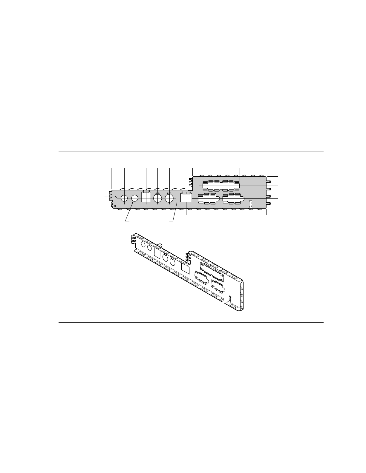
BL440ZX Motherboard Technical Product Specification
1.15.2 I/O Shield
The back panel I/O shield for the motherboard must meet specific dimension and material
requirements. Systems based on this motherboard need the I/O shield to pass certification testing.
Figure 5 shows the shield’s critical dimensions in inches. The figure indicates the position of each
cutout. Additional design considerations for I/O shields relative to chassis requirements are
described in the NLX Motherboard Specification. See Section 6.2 for information about the
specification.
NOTE
✏
A back panel I/O shield designed to be compliant with the NLX Motherboard Specification is
available from Intel (see Section 6.2 for the version of the specification supported).
0.948
0.456
0.00
0.168
0.00
0.570
2.504
1.838
1.175
0.366(2) 0.240
3.179
5.532
4.165
Figure 5. Back Panel I/O Shield Dimensions
5.997
7.274
7.429
1.752
1.197
0.447
0.143
8.853
OM08466
42
Page 43

Motherboard Description
1.16 Electrical Considerations
1.16.1 Power Consumption
Table 21 lists the power usage for a computer that contains a motherboard with a Celeron
processor operating at 333 MHz, 128 KB cache, 64 MB SDRAM, 1.44 MB floppy drive, 1.6 GB
IDE hard drive, 24X IDE CD-ROM, and integrated ATI RAGE PRO TURBO 2X AGP controller
with 8 MB of video memory. This information is provided only as a guide for calculating
approximate power usage with additional resources added.
†
Values for the Windows
watts are measured with a typical 200 W power supply, nominal input voltage and frequency, and
with a true RMS wattmeter at the line input.
Table 21. Power Usage
Mode AC (Watts) +3.3 V +5 V +12 V -12 V +5 VSB
DOS prompt 29.07 W 1.52 A 2.12 A 0.37 A 0.01 A 0.12 A
Windows 95 desktop, APM disabled 29.07 W 1.27 A 2.81 A 0.34 A 0.01 A 0.13 A
Windows 95 desktop, APM enabled, in
System Management Mode (SMM)
95 desktop mode are measured at 256 colors and 60 Hz refresh rate. AC
DC (Amps) at:
16.96 W 1.20 A 0.53 A 0.21 A 0.02 A 0.11 A
The processor fan requires +12 V in both Full On and Standby modes. The maximum current
draw on +12 V at the fan header is 250 mA.
43
Page 44

BL440ZX Motherboard Technical Product Specification
1.16.2 Power Supply Considerations
System integrators should refer to the power usage values listed in Table 21 when selecting a
power supply for use with this motherboard. The power supply must comply with the parameters
listed in the NLX Power Supply Recommendations and NLX Motherboard Specification for the
following:
• The potential relation between 3.3 VDC and +5 VDC power rails
• The current capability of the +5 VSB (standby) line
• All timing parameters
• All voltage tolerances (see Table 22)
• NLX 20-pin power connector
• Soft-Off support
See Section 6.2 for specification information.
Table 22. DC Voltage Tolerances
DC Voltage Acceptable Tolerance
+3.3 V ± 4%
+5 V ± 5%
+5 VSB (standby) ± 5%
-5 V ± 5%
+12 V ± 5%
-12 V ± 5%
CAUTION
The motherboard requires at least 720 mA of +5 VSB to support Soft-Off and the following
wake-up events: LAN and Ring (modem). If standby current is inadequate, the motherboard may
fail to wake or, in the case of Soft-Off, fail to power down.
44
Page 45

Motherboard Description
1.17 Thermal Considerations
Table 23 lists maximum component case temperatures for motherboard components that could be
sensitive to thermal changes. Case temperatures could be affected by factors such as the operating
temperature, current load, or operating frequency. Maximum case temperatures are important
when considering proper airflow to cool the motherboard.
Table 23. Thermal Considerations for Components
Component Maximum Case Temperature Motherboard Location
Intel Celeron processor 300A MHz
333 MHz
366 MHz
Intel 82443ZX PAC 105 oC U3E1
Intel 82371EB PIIX4E 85 oC U7D1
CAUTION
An ambient temperature that exceeds the motherboard’s maximum operating temperature might
cause components to exceed their maximum case temperature. For information about the
motherboard’s maximum operating temperature, see the environmental specifications in
Section 1.18.
85 oC
85 oC
85 oC
J3B1
45
Page 46

BL440ZX Motherboard Technical Product Specification
Figure 6 shows motherboard components that may be sensitive to thermal changes.
A
B
A Intel 82443ZX PAC
B Intel 82371EB PIIX4E
C Intel Celeron processor
Figure 6. Thermally-sensitive Components
C
OM07461
46
Page 47

1.18 Environmental Specifications
Table 24. Environmental Specifications
Parameter Specification
Temperature
Nonoperating -40° C to +70° C
Operating 0 °C to +55 °C
Shock
Unpackaged 30 g trapezoidal waveform
Velocity change of 170 inches/sec
Packaged Half sine 2 millisecond
Product Weight
(lbs)
<20 36 167
21-40 30 152
41-80 24 136
81-100 18 118
Vibration
Unpackaged 5 Hz to 20 Hz : 0.01 g² Hz sloping up to 0.02 g² Hz
20 Hz to 500 Hz : 0.02 g² Hz (flat)
Packaged 10 Hz to 40 Hz : 0.015 g² Hz (flat)
40 Hz to 500 Hz : 0.015 g² Hz sloping down to 0.00015 g² Hz
Free Fall (inches) Velocity Change (inches/sec)
Motherboard Description
1.19 Reliability
The mean time between failures (MTBF) prediction is calculated using component and
subassembly random failure rates. The calculation is based on the Bellcore Reliability Prediction
Procedure, TR-NWT-000332, Issue 4, September 1991. The MTBF prediction is for estimating
repair rates and spare parts requirements.
MTBF data is calculated from predicted data at 55 °C.
The MTBF prediction for the motherboard is 138,150 hours.
47
Page 48

BL440ZX Motherboard Technical Product Specification
1.20 Regulatory Compliance
This motherboard complies with the following safety and EMC regulations when correctly
installed in a compatible host system.
Table 25. Safety Regulations
Regulation Title
UL 1950/CSA950, 3rd edition, Dated
07-28-95
EN 60950, 2nd Edition, 1992 (with
Amendments 1, 2, 3, and 4)
IEC 950, 2nd edition, 1991 (with
Amendments 1, 2, 3, and 4)
EMKO-TSE (74-SEC) 207/94 Summary of Nordic deviations to EN 60950. (Norway, Sweden,
Table 26. EMC Regulations
Bi-National Standard for Safety of Information Technology
Equipment including Electrical Business Equipment. (USA and
Canada)
The Standard for Safety of Information Technology Equipment
including Electrical Business Equipment. (European Community)
The Standard for Safety of Information Technology Equipment
including Electrical Business Equipment. (International)
Denmark, and Finland)
Regulation Title
FCC Class B Title 47 of the Code of Federal Regulations, Parts 2 and 15,
Subpart B, pertaining to unintentional radiators. (USA)
CISPR 22, 2nd Edition, 1993
(Class B)
VCCI Class B (ITE) Implementation Regulations for Voluntary Control of Radio
EN55022 (1994) (Class B) Limits and methods of measurement of Radio Interference
EN50082-1 (1992) Generic Immunity Standard; Currently compliance is determined via
ICES-003 (1997) Interference-Causing Equipment Standard, Digital Apparatus,
ICES-003, Issue 2 Interference-Causing Equipment Standard, Digital Apparatus.
Limits and methods of measurement of Radio Interference
Characteristics of Information Technology Equipment.
(International)
Interference by Data Processing Equipment and Electronic Office
Machines. (Japan)
Characteristics of Information Technology Equipment. (Europe)
testing to IEC 801-2, -3, and -4. (Europe)
Class B (Including CRC c.1374) (Canada)
(Canada)
This printed circuit assembly has the following product certification markings:
• UL Joint Recognition Mark: Consists of small c followed by a stylized backward UR and
followed by a small US (component side).
• Manufacturer’s recognition mark: Consists of a unique UL-recognized manufacturer’s logo,
along with a flammability rating (94V-0) (solder side).
• UL File Number for motherboards: E139761 (component side).
• PB Part Number: Intel bare circuit board part number 721282-001 (solder side).
• Battery “+ Side Up” marking: Located on the component side of the motherboard in close
proximity to the battery holder.
• FCC Logo/Declaration: Located on the solder side of the motherboard.
• CE Mark: Located on the component side of the motherboard and on the shipping container.
48
Page 49

2 Motherboard Resources
What This Chapter Contains
2.1 Memory Map ............................................................................................................. 49
2.2 DMA Channels .......................................................................................................... 50
2.3 I/O Map ..................................................................................................................... 50
2.4 PCI Configuration Space Map ................................................................................... 52
2.5 Interrupts...................................................................................................................53
2.6 PCI Interrupt Routing Map......................................................................................... 54
2.1 Memory Map
Table 27. System Memory Map
Address Range (decimal) Address Range (hex) Size Description
1024 K - 262144 K 100000 - FFFFFFF 255 MB Extended Memory
960 K - 1024 K F0000 - FFFFF 64 KB Runtime BIOS
896 K - 960 K E0000 - EFFFF 64 KB Reserved
800 K - 896 K C8000 - DFFFF 96 KB Available high DOS memory (open
to ISA and PCI bus)
640 K - 800 K A0000 - C7FFF 160 KB Video memory and BIOS
639 K - 640 K 9FC00 - 9FFFF 1 KB Extended BIOS data (movable by
memory manager software)
512 K - 639 K 80000 - 9FBFF 127 KB Extended conventional memory
0 K - 512 K 00000 - 7FFFF 512 KB Conventional memory
49
Page 50

BL440ZX Motherboard Technical Product Specification
2.2 DMA Channels
Table 28. DMA Channels
DMA Channel Number Data Width System Resource
0 8- or 16-bits Audio
1 8- or 16-bits Audio / parallel port
2 8- or 16-bits Diskette drive
3 8- or 16-bits Parallel port (for ECP or EPP)/audio
4 Reserved—cascade channel
5 16-bits Open
6 16-bits Open
7 16-bits Open
2.3 I/O Map
Table 29. I/O Map
Address (hex) Size Description
0000 - 000F 16 bytes PIIX4E—DMA 1
0020 - 0021 2 bytes PIIX4E—interrupt controller 1
0040 - 0043 4 bytes PIIX4E—counter/timer 1
0048 - 004B 4 bytes PIIX4E—counter/timer 2
0060 1 byte Keyboard controller byte—reset IRQ
0061 1 byte PIIX4E—NMI, speaker control
0064 1 byte Keyboard controller, CMD/STAT byte
0070, bit 7 1 bit PIIX4E—enable NMI
0070, bits 6:0 7 bits PIIX4E—real time clock, address
0071 1 byte PIIX4E—real time clock, data
0070 -0071 2 bytes CMOS Bank 0
0072 - 0073 2 bytes CMOS Bank 1
0080 - 008F 16 bytes PIIX4E—DMA page registers
00A0 - 00A1 2 bytes PIIX4E—interrupt controller 2
00B2 - 00B3 2 bytes APM control
00C0 - 00DE 31 bytes PIIX4E—DMA 2
00F0 1 byte Reset numeric error
0170 - 0177 8 bytes Secondary IDE channel
01F0 - 01F7 8 bytes Primary IDE channel
continued
50
Page 51

Table 29. I/O Map (continued)
Address (hex) Size Description
One of the
following ranges:
0200 - 0207
0208 - 020F
0210 - 0217
0218 - 021F
One of the
following ranges:
0220 - 022F
0240 - 024F
0278 - 027F* 8 bytes LPT2
0228 - 022F* 8 bytes LPT3
02E8 - 02EF* 8 bytes COM4/video (8514A)
02F8 - 02FF* 8 bytes COM2
One of the
following ranges:
0320 - 0327
0330 - 033F
0340 - 0347
0350 - 0357
0376 1 byte Secondary IDE channel command port
0377, bits 6:0 7 bits Secondary IDE channel status port
0378 - 037F 8 bytes LPT 1
0388- 038B 4 bytes AdLib† (FM synthesizer)
03B4 - 03B5 2 bytes Video (VGA)
03BA 1 byte Video (VGA)
03C0 - 03CA 2 bytes Video (VGA)
03CC 1 byte Video (VGA)
03CE - 03CF 2 bytes Video (VGA)
03D4 - 03D5 2 bytes Video (VGA)
03DA 1 byte Video (VGA)
03E8 - 03EF 8 bytes COM3
03F0 - 03F5 6 bytes Diskette channel 1
03F6 1 byte Primary IDE channel command port
03F7 (Write) 1 byte Diskette channel 1 command
03F7, bit 7 1 bit Diskette change, channel 1
03F7, bits 6:0 7 bits Primary IDE channel status port
03F8 - 03FF 8 bytes COM1
04D0 - 04D1 2 bytes Edge/level triggered PIC
Note 1. Default, but can be changed to another address range.
8 bytes Audio / game port
16 bytes Audio (Sound Blaster Pro compatible)
8 bytes MPU-401 (MIDI)
Motherboard Resources
continued
51
Page 52

BL440ZX Motherboard Technical Product Specification
Table 29. I/O Map (continued)
Address (hex) Size Description
LPTn + 400h 8 bytes ECP port, LPTn base address + 400h
0CF8 - 0CFB* 4 bytes PCI configuration address register
0CF9** 1 byte Turbo and reset control register
0CFC - 0CFF 4 bytes PCI configuration data register
FFA0 - FFA7 8 bytes Primary bus master IDE registers
FFA8 - FFAF 8 bytes Secondary bus master IDE registers
32 contiguous bytes starting on a
32-byte divisible boundary
64 contiguous bytes starting on a
64-byte divisible boundary
Notes (continued):
2. Dword access only
3. Byte access only
Intel 82559 LAN controller
Onboard audio controller
2.4 PCI Configuration Space Map
Table 30. PCI Configuration Space Map
Bus
Number (hex)
00 00 00 Intel 82443ZX (PAC)
00 01 00 Intel 82443ZX PCI/AGP bridge
00 06 00 Intel 82559 LAN controller
00 07 00 Intel 82371EB (PIIX4E) PCI/ISA bridge
00 07 01 Intel 82371EB (PIIX4E) IDE bus master
00 07 02 Intel 82371EB (PIIX4E) USB
00 07 03 Intel 82371EB (PIIX4E) power management
00 0C 00 PCI audio controller (Creative Sound Blaster
00 14 00 PCI expansion slot 1 *
00 12 00 PCI expansion slot 2 *
00 10 00 PCI expansion slot 3 *
00 0E 00 PCI expansion slot 4 *
01 00 00 ATI RAGE PRO TURBO 2X AGP graphics controller
* The number of PCI expansion slots supported depends on the riser card configuration and the number of PCI bus
masters on the motherboard. See Table 14 to determine how many PCI bus masters are available for the riser card.
Device
Number (hex)
Function
Number (hex) Description
AudioPCI 64V)
52
Page 53

2.5 Interrupts
Table 31. Interrupts
IRQ System Resource
NMI I/O channel check
0 Reserved, interval timer
1 Reserved, keyboard buffer full
2 Reserved, cascade interrupt from slave PIC
3 COM2* (user available if COM2 is not present)
4 COM1*
5 LPT2 (Plug and Play option) / audio / user available
6 Diskette drive controller
7 LPT1*
8 Real time clock
9 Reserved for PIIX4E system management bus
10 User available
11 User available
12 Onboard mouse port (if present, else user available)
13 Reserved, math coprocessor
14 Primary IDE (if present, else user available)
15 Secondary IDE (if present, else user available)
* Default, but can be changed to another IRQ
Motherboard Resources
53
Page 54

BL440ZX Motherboard Technical Product Specification
2.6 PCI Interrupt Routing Map
This section describes interrupt sharing and how the interrupt signals are connected between the
‡
PCI expansion slots
be shared between devices attached to the PCI bus. In most cases, the small amount of latency
added by interrupt sharing does not affect the operation or throughput of the devices. In some
special cases where maximum performance is needed from a device, a PCI device should not share
an interrupt with other PCI devices. Use the following information to avoid sharing an interrupt
with a PCI add-in card.
PCI devices are categorized as follows to specify their interrupt grouping:
• INTA: By default, all add-in cards that require only one interrupt are in this category. For
almost all cards that require more than one interrupt, the first interrupt on the card is also
classified as INTA.
• INTB: Generally, the second interrupt on add-in cards that require two or more interrupts is
classified as INTB. (This is not an absolute requirement.)
• INTC and INTD: Generally, a third interrupt on add-in cards is classified as INTC and a
fourth interrupt is classified as INTD.
and onboard PCI devices. The PCI specification specifies how interrupts can
The PIIX4E PCI-to-ISA bridge has four programmable interrupt request (PIRQ) input signals.
Any PCI interrupt source (either onboard or from a PCI add-in card) connects to one of these PIRQ
signals. Because there are only four signals, some PCI interrupt sources are mechanically tied
together on the motherboard and therefore share the same interrupt. Table 32 shows an example of
how the PIRQ signals might be connected to a riser card’s PCI expansion slots and to onboard PCI
interrupt sources.
Table 32. PCI Interrupt Routing Map
First PCI
PIIX4 PIRQ
Signal
PIRQA INTA INTB INTC INTD INTA
PIRQB INTB INTC INTD INTA INTA
PIRQC INTC INTD INTA INTB
PIRQD INTD INTA INTB INTC INTD INTA
* The number of PCI expansion slots supported depends on the riser card configuration and the number of PCI bus
masters on the motherboard. See Table 14 to determine how many PCI bus masters are available for the riser card.
Expansion
Slot *
Second PCI
Expansion
Slot *
Third PCI
Expansion
Slot *
Fourth PCI
Expansion
Slot *
Onboard
Video
PCI
Audio USB
LAN
Controller
Using the example shown in Table 32, assume an add-in card with one interrupt (group INTA) is
inserted into the second PCI slot. In this slot, an interrupt source from group INTA connects to the
PIRQD signal, which is already connected to the LAN PCI source. The add-in card shares an
interrupt with this onboard interrupt source.
NOTE
✏
The PIIX4E can connect each PIRQ line internally to one of the IRQ signals (3, 4, 5, 7, 11, 14, 15).
Typically, a device that does not share a PIRQ line will have a unique interrupt. However, in
certain interrupt-constrained situations, it is possible for two or more of the PIRQ lines to be
connected to the same IRQ signal.
54
Page 55

3 Overview of BIOS Features
What This Chapter Contains
3.1 Introduction................................................................................................................ 55
3.2 BIOS Flash Memory Organization............................................................................. 56
3.3 Resource Configuration............................................................................................. 56
3.4 System Management BIOS (SMBIOS)...................................................................... 57
3.5 Power Management .................................................................................................. 58
3.6 BIOS Upgrades ......................................................................................................... 60
3.7 Recovering BIOS Data .............................................................................................. 61
3.8 Boot Options.............................................................................................................. 62
3.9 USB Legacy Support................................................................................................. 63
3.10 BIOS Security Features............................................................................................. 64
3.1 Introduction
The motherboard uses an Intel/AMI BIOS, which is stored in flash memory and can be upgraded
using a disk-based program. The flash memory also contains the Setup program, POST, APM,
PCI autoconfiguration utility, and Windows 95-ready Plug and Play. See Section 6.2 for the
supported versions of APM and Plug and Play.
This motherboard supports system BIOS shadowing, allowing the BIOS to execute from 64-bit
onboard write-protected DRAM.
The BIOS displays a message during POST identifying the type of BIOS and a revision code. The
initial production BIOS is identified as 4B4LZ0XA.86A.
55
Page 56

BL440ZX Motherboard Technical Product Specification
3.2 BIOS Flash Memory Organization
The Intel E28F200B5 2-Mbit flash component is organized as 256 KB x 8 bits and is divided into
areas as described in Table 33. The table shows the addresses in the ROM image in BIOS normal
mode (the addresses change in BIOS recovery mode).
Table 33. Flash Memory Organization
Address (Hex) Size Description
FFFFC000 - FFFFFFFF 16 KB Boot Block
FFFFA000 - FFFFBFFF 8 KB Vital Product Data (VPD), Extended System Configuration Data
(ESCD) (SMBIOS configuration data / Plug and Play data)
FFFF9000 - FFFF9FFF 4 KB Used by the BIOS for activities such as event logging
FFFF8000 - FFFF8FFF 4 KB OEM logo or scan flash area
FFFC0000 - FFFF7FFF 224 KB Main BIOS block
3.3 Resource Configuration
3.3.1 Plug and Play: PCI Autoconfiguration
The BIOS can automatically configure PCI devices and Plug and Play devices. PCI devices may
be onboard or add-in cards. Plug and Play devices are ISA devices built to meet the Plug and Play
specification. Autoconfiguration lets a user insert or remove PCI or Plug and Play cards without
having to configure the system. When a user turns on the system after adding a PCI or Plug and
Play card, the BIOS automatically configures interrupts, the I/O space, and other system resources.
Any interrupts set to Available in Setup (see Section 4.4.8) are considered to be available for use
by the add-in card.
PCI interrupts are distributed to available ISA interrupts that have not been assigned to an ISA
card or to system resources. The assignment of PCI interrupts to ISA IRQs is nondeterministic.
PCI devices can share an interrupt, but an ISA device cannot share an interrupt allocated to a PCI
device or to another ISA device. Autoconfiguration information is stored in ESCD format.
For information about the versions of PCI and Plug and Play supported by this BIOS, see
Section 6.2.
3.3.2 ISA Plug and Play
If the user selects Plug & Play OS in Setup (see Section 4.4.1), the BIOS autoconfigures only ISA
Plug and Play cards that are required for booting (IPL devices). If Plug and Play operating system
is not selected in Setup, the BIOS autoconfigures all Plug and Play ISA cards. Because ISA legacy
devices are not autoconfigurable, the resources for them must be reserved in BIOS Setup.
56
Page 57

Overview of BIOS Features
3.3.3 PCI IDE Support
If the user selects Auto in Setup (see Section 4.4.4), the BIOS automatically sets up the two PCI
IDE connectors with independent I/O channel support. The IDE interface supports hard drives up
to PIO Mode 4 and recognizes any ATAPI devices, including CD-ROM drives, tape drives, and
Ultra DMA drives (see Section 6.2 for the supported version of ATAPI). Add-in ISA IDE
controllers are not supported. The BIOS determines the capabilities of each drive and configures
them to optimize capacity and performance. You can override the autoconfiguration option by
specifying User configuration in the IDE Configuration Submenu of Setup.
NOTE
✏
Do not connect an ATA device as a slave on the same IDE cable as an ATAPI master device.
3.4 System Management BIOS (SMBIOS)
SMBIOS is an interface for managing computers in an enterprise environment. The main
component of SMBIOS is the management information format (MIF) database, which contains
information about the computing system and its components. Using SMBIOS, a system
administrator can obtain the system types, capabilities, operational status, and installation dates for
system components. The MIF database defines the data and provides the method for accessing this
information. The BIOS enables applications such as Intel LANDesk Client Manager to use
SMBIOS. The BIOS stores and reports the following SMBIOS information:
• BIOS data, such as the BIOS revision level
• Fixed-system data, such as peripherals, serial numbers, and asset tags
• Resource data, such as memory size, cache size, and processor speed
• Dynamic data, such as event detection and error logging
Intel can provide system manufacturers with a utility that programs system- and chassis-related
information into the SMBIOS space in flash memory. The utility is used to program the BIOS
during system manufacturing, so that the BIOS can later report this information. Once written, this
information cannot be overwritten by the end user.
†
Non-Plug and Play operating systems, such as Windows NT
obtaining SMBIOS information. The BIOS supports an SMBIOS table interface for such
operating systems. Using this support, a SMBIOS service-level application running on a non-Plug
and Play operating system can access the SMBIOS BIOS information.
See Section 6.2 for SMBIOS specification information.
, require an additional interface for
57
Page 58

BL440ZX Motherboard Technical Product Specification
3.5 Power Management
3.5.1 APM
The BIOS supports both APM and ACPI. If the board is used with an ACPI-aware operating
system, the BIOS provides ACPI support. Otherwise, it defaults to APM support.
See Section 6.2 for the version of the APM specification that is supported. The energy saving
standby mode can be initiated in the following ways:
• Time-out period specified in Setup
• Suspend/resume switch connected to the front panel sleep connector
• From the operating system, such as the Suspend menu item in Windows 95
In standby mode, the motherboard can reduce power consumption by spinning down hard drives,
and reducing power to or turning off VESA
†
DPMS-compliant monitors. Power-management
mode can be enabled or disabled in Setup (see Section 4.6).
While in standby mode, the system retains the ability to respond to external interrupts and service
requests, such as incoming faxes or network messages. Any keyboard or mouse activity brings the
system out of standby mode and immediately restores power to the monitor.
‡
The BIOS enables APM by default; but the operating system must support an APM driver for the
power-management features to work. For example, Windows 95 supports the power-management
features upon detecting that APM is enabled in the BIOS.
3.5.2 ACPI
ACPI gives the operating system direct control over the power management and Plug and Play
functions of a computer. ACPI requires an ACPI-aware operating system. ACPI features include:
• Plug and Play (including bus and device enumeration) and APM functionality normally
contained in the BIOS
• Power management control of individual devices, add-in boards (some add-in boards may
require an ACPI-aware driver), video displays, and hard disk drives
• Methods for achieving less than 30-watt system operation in the Power On Suspend sleeping
state, and less than 5-watt system operation in the Suspend to Disk sleeping state
• A Soft-Off feature that enables the operating system to power off the computer
• Support for wake-up events (see Table 36)
‡
• Support for a front panel power and sleep mode switch
based on how long the power switch is pressed, depending on how ACPI is configured with an
ACPI-aware operating system
. Table 34 describes the system states
58
Page 59

Overview of BIOS Features
Table 34. Effects of Pressing the Power Switch
…and the power switch is
If the system is in this state…
Off Less than four seconds Power on
On Less than four seconds Soft-Off/Suspend
On More than four seconds Fail safe power off
Sleep Less than four seconds Wake-up
pressed for …the system enters this state
3.5.2.1 System States and Power States
Under ACPI, the operating system directs all system and device power state transitions. The
operating system puts devices in and out of low-power states based on user preferences and
knowledge of how devices are being used by applications. Devices that are not being used can be
turned off. The operating system uses information from applications and user settings to put the
system as a whole into a low-power state.
Table 35 lists the power states supported by the motherboard along with the associated system
power targets. See the ACPI specification for a complete description of the various system and
power states.
Table 35. Power States and Targeted System Power
Processor
Global States Sleeping States
G0—working
state
G1—sleeping
state
G2/S5 S5—Soft-Off.
G3—
mechanical off.
AC power is
disconnected
from the
computer.
* Total system power depends on the system configuration, including add-in boards and peripherals powered by the
system chassis’ power supply.
** Depends the standby power consumption of wake-up devices used in the system.
S0—working C0—working D0—working state Full power > 60 W
S1—processor
stopped
Context not
saved. Cold boot
is required.
No power to the
system.
States Device States Targeted System Power *
C1—stop grant D1, D2, D3—
device
specification
specific.
No power D3—no power
except for
wake-up logic.
No power D3—no power for
wake-up logic,
except when
provided by
battery or external
source.
5 W < power < 30 W
Power < 5 W **
No power to the system so
that service can be
performed.
59
Page 60

BL440ZX Motherboard Technical Product Specification
3.5.2.2 Wake-up Devices and Events
Table 36 describes which devices or specific events can wake the computer from specific ACPI
states. Sleeping states S4BIOS and S5 are the same for the wake-up events.
Table 36. Wake-up Devices and Events
These devices/events can
wake-up the computer… …from this ACPI state
Power switch S1, S5
RTC alarm S1, S5
LAN S1
Ring (modem) S1
USB S1
PS/2 keyboard S1
PS/2 mouse S1
3.5.2.3 Plug and Play
In addition to power management, ACPI provides controls and information so that the operating
system can facilitate Plug and Play device enumeration and configuration. ACPI is used to
enumerate and configure only those motherboard devices that do not have other hardware
standards for enumeration and configuration. PCI devices on the motherboard, for example, are
not enumerated by ACPI.
3.6 BIOS Upgrades
A new version of the BIOS can be upgraded from a diskette using the Intel® Flash Memory Update
utility that is available from Intel. This utility supports the following BIOS maintenance functions:
• Update the flash BIOS from a file on a diskette.
• Change the language section of the BIOS.
• Verify that the upgrade BIOS matches the target system to prevent accidentally installing an
incompatible BIOS.
BIOS upgrades and the Intel Flash Memory Update utility are available from Intel through the
Intel World Wide Web site. See Section 6.1 for information about this site.
NOTE
✏
Please review the instructions distributed with the upgrade utility before attempting a BIOS
upgrade.
60
Page 61

Overview of BIOS Features
3.6.1 Language Support
The Setup program and help messages can be supported in 32 languages. Five languages are
available in the BIOS: American English, German, Italian, French, and Spanish. The default
language is American English, which is present unless another language is selected in BIOS Setup.
The BIOS includes extensions to support the Kanji character set and other non-ASCII character
sets. Translations of other languages may become available at a later date.
3.6.2 OEM Logo or Scan Area
A 4 KB flash-memory user area is available for displaying a custom OEM logo during POST. A
utility is available from Intel to assist with installing a logo into the flash memory. Information
about this capability is available on the Intel Support World Wide Web site. See Section 6.1 for
more information about this site.
3.7 Recovering BIOS Data
Some types of failure can destroy the BIOS. For example, the data can be lost if a power outage
occurs while the BIOS is being updated in flash memory. To recover the BIOS from a diskette, the
user must set the BIOS Setup configuration jumper block to recovery mode (see Table 20). When
recovering the BIOS, the user must be aware of the following:
• Because of the small amount of code available in the nonerasable boot block area, there is no
video support. The procedure can be monitored only by listening to the speaker and looking at
the diskette drive LED.
• The recovery process may take several minutes; larger BIOS flash memory devices require
more time.
• Two beeps and the end of activity in the diskette drive indicate successful BIOS recovery.
• A series of continuous beeps indicates a failed BIOS recovery.
To create a BIOS recovery diskette, a bootable diskette must be created and the recovery files
copied to it. The recovery files are available from Intel. See Section 6.1 for information on
contacting Intel customer support for more information.
CAUTION
BIOS recovery cannot be done using non-SPD DIMMs. SPD data structure is required for the
recovery process.
NOTE
✏
If the computer is configured to recover the BIOS from an diskette in an LS-120 (see
Sections 1.4.2.2 and 4.7), the BIOS recovery diskette must be a standard 1.44 MB diskette, not a
120 MB diskette.
61
Page 62

BL440ZX Motherboard Technical Product Specification
3.8 Boot Options
In the Setup program, the user can choose to boot from a diskette drive, hard drives, CD-ROM, or
the network. The default setting is for the diskette drive to be the primary boot device and the hard
drive to be the secondary boot device. By default the third and fourth devices are disabled.
3.8.1 CD-ROM and Network Boot
Booting from CD-ROM is supported in compliance with the El Torito bootable CD-ROM format
specification. See Section 6.2 for information about the El Torito specification. Under the Boot
menu in the Setup program, ATAPI CD-ROM is listed as a boot device. Boot devices are defined
in priority order. If the CD-ROM is selected as the boot device, it must be the first device.
The network can be selected as a boot device. This selection allows booting from a network add-in
card with a remote boot ROM installed.
3.8.2 Booting Without Attached Devices
For use in embedded applications, the BIOS has been designed so that after passing the POST, the
operating system loader is invoked even if no video adapter, keyboard, or mouse is attached.
3.8.3 Default Settings After Battery and Power Failure
If the battery and AC power fail, standard defaults, not custom defaults, will be loaded into CMOS
RAM at power on.
62
Page 63

Overview of BIOS Features
3.9 USB Legacy Support
USB legacy support enables a USB keyboard or mouse to be used when no operating system USB
driver is in place. USB legacy support is intended to be used only in accessing BIOS Setup and
installing an operating system that supports USB.
To install an operating system that supports USB, set USB legacy support in BIOS Setup to Auto,
and follow the operating system’s installation instructions. This sequence describes how USB
legacy support operates in the default (Auto) mode.
1. When the user powers up the computer, USB legacy support is set to Auto in Setup.
2. The POST begins.
3. If the POST detects a USB keyboard, the BIOS enables the keyboard to be used to enter the
Setup program or maintenance mode.
4. After the operating system loads, the USB keyboard and mouse will be usable and controlled
by the BIOS until a USB driver takes control.
NOTES
✏
If USB legacy support is enabled, do not mix USB and PS/2 keyboards and mice. For example, do
not use a PS/2 keyboard with a USB mouse, or a USB keyboard and a PS/2 mouse.
Do not use USB devices with an operating system that does not support USB. USB legacy is not
intended to support the use of USB devices in a non-USB aware operating system.
USB legacy support is for keyboards and mice only. Hubs and other USB devices are not
supported.
63
Page 64

BL440ZX Motherboard Technical Product Specification
3.10 BIOS Security Features
The BIOS includes security features that restrict access to the BIOS Setup program and restrict
who can boot the computer. A supervisor password and a user password can be set for accessing
the Setup program and for booting the computer, with the following restrictions:
• The supervisor password gives unrestricted access to view and change all the Setup options in
the Setup program. This is supervisor mode.
• The user password gives restricted access to view and change Setup options in the Setup
program. This is user mode.
• If only the supervisor password is set, pressing the <Enter> key at the password prompt of the
Setup program allows the user restricted access to Setup.
• If both the supervisor and user passwords are set, users can enter either the supervisor
password or the user password to access Setup. Users have access to Setup respective to
which password is entered.
• Setting the user password restricts who can boot the computer. The password prompt will be
displayed before the computer is booted. If only the administrator password is set, the
computer boots without asking for a password. If both passwords are set, the user can enter
either password to boot the computer.
Table 37 shows the effects of setting the supervisor password and user password. This table is for
reference only and is not displayed on the screen.
Table 37. Supervisor and User Password Functions
Supervisor
Password Set
Neither Can change all
Supervisor
only
User only N/A Can change all
Supervisor
and user set
* If no password is set, any user can change all Setup options.
Mode User Mode Setup Options
options *
Can change all
options
Can change all
options
Can change all
options *
Can change a
limited number
of options
options
Can change a
limited number
of options
None None None
Supervisor Password Supervisor None
Enter Password
Clear User Password
Supervisor Password
Enter Password
Password to
Enter Setup
User User
Supervisor or
user
Password
During Boot
Supervisor or
user
See Section 4.5 for information about setting user and supervisor passwords.
64
Page 65

4 BIOS Setup Program
What This Chapter Contains
4.1 Introduction................................................................................................................ 65
4.2 Maintenance Menu.................................................................................................... 66
4.3 Main Menu................................................................................................................. 67
4.4 Advanced Menu......................................................................................................... 68
4.5 Security Menu............................................................................................................ 73
4.6 Power Menu.............................................................................................................. 74
4.7 Boot Menu................................................................................................................. 74
4.8 Exit Menu .................................................................................................................. 75
4.1 Introduction
The Setup program is used for viewing and changing the BIOS settings for a computer. The user
accesses Setup by pressing the <F2> key after the Power-On Self Test (POST) memory test begins
and before the operating system boot begins.
Table 38 shows the menus available from the menu bar at the top of the Setup screen.
Table 38. Setup Menu Bar
Setup Menu Screen Description
Maintenance Displays the processor speed. Clears the Setup passwords. This menu
is available only in configure mode. Refer to Section 1.14.2 for
information about configure mode.
Main Allocates resources for hardware components.
Advanced Specifies advanced features available through the chipset.
Security Specifies passwords and security features.
Power Specifies power management features.
Boot Specifies boot options and power supply controls.
Exit Saves or discards changes to the Setup program options.
65
Page 66

BL440ZX Motherboard Technical Product Specification
Table 39 shows the function keys available for menu screens.
Table 39. Setup Function Keys
Setup Key Description
<←> or <→> Selects a different menu screen.
<↑> or <↓> Moves cursor up or down.
<Enter> Executes command or selects the submenu.
<F9> Loads the default configuration values for the current menu.
<F10> Saves the current values and exits Setup.
<Esc> Exits the menu.
<F1> Displays online help.
4.2 Maintenance Menu
This menu is used for setting the processor speed and clearing the Setup passwords. Setup
displays this menu only in configure mode. See Section 1.14.2 for information about setting
configure mode.
Table 40. Maintenance Menu
Feature Options Description
Processor Speed No options Displays the processor speed in megahertz
With a host bus operating at 66 MHz, the board supports processors
at the following speeds: 300A, 333, and 366 MHz
Clear All Passwords No options Clears the user and supervisor passwords
66
Page 67

BIOS Setup Program
4.3 Main Menu
This menu reports processor and memory information. This menu is used to set the system date
and system time.
Table 41. Main Menu
Feature Options Description
BIOS Version No options Displays the version of the BIOS.
Processor Type No options Displays processor type.
Processor Speed No options Displays processor speed.
Cache RAM No options Displays the size of second-level cache.
Total Memory No options Displays the total amount of RAM on the motherboard.
Bank 0
Bank 1
Language • English (US)
Cache Bus ECC
Memory
Configuration
System Time Hour, minute, and
System Date Month, day, and year Specifies the current date.
No options Displays the type of DIMM installed in each memory bank.
Selects the default language used by the BIOS.
(default)
• German
• French
• Italian
• Spanish
N/A
Non-ECC Not applicable
second
Not applicable
Specifies the current time.
67
Page 68

BL440ZX Motherboard Technical Product Specification
4.4 Advanced Menu
This menu is used for setting advanced features that are available through the chipset.
Table 42. Advanced Menu
Feature Options Description
Boot Settings
Configuration
Peripheral Configuration No options Configures peripheral ports and devices. When selected,
IDE Configuration No options Specifies type of connected IDE device.
Diskette Configuration No options When selected, displays the Diskette Configuration
Event Log Configuration No options Configures Event Logging. When selected, displays the
Video Configuration No options Configures video features. When selected, displays the
Resource Configuration No options Configures memory blocks and IRQs for legacy ISA devices.
No options Configures Plug and Play and the Numlock key, and resets
configuration data. When selected, displays the Boot
Settings Configuration submenu.
displays the Peripheral Configuration submenu.
submenu.
Event Log Configuration submenu.
Video Configuration submenu.
When selected, displays the Resource Configuration
submenu.
4.4.1 Boot Setting Configuration Submenu
This menu is used for setting Plug and Play and the Numlock key, and for resetting configuration
data.
Table 43. Boot Setting Configuration Submenu
Feature Options Description
Plug & Play O/S
Reset Config Data
NumLock Off
No (default)
Yes
No (default)
Yes
On (default)
Specifies if a Plug and Play operating system is being used.
No
lets the BIOS configure all devices.
Yes
lets the operating system configure Plug and Play
devices. Not required with a Plug and Play operating
system.
Clears the BIOS configuration data on the next boot.
Specifies the power on state of the Numlock feature on the
numeric keypad of the keyboard.
68
Page 69

4.4.2 Peripheral Configuration Submenu
This submenu is used for configuring the computer peripherals.
Table 44. Peripheral Configuration Submenu
Feature Options Description
Serial port A • Disabled
• Enabled
• Auto (default)
Base I/O address • 3F8 (default)
• 3E8
• 2E8
Interrupt • IRQ 3
• IRQ 4 (default)
Parallel port • Disabled
• Enabled
• Auto (default)
Mode • Output Only
• Bidirectional
(default)
• EPP
• ECP
Base I/O address
Interrupt • IRQ 5 (default)
Audio • Disabled
Legacy USB Support • Disabled
LAN • Disabled
• 378 (default)
• 278
• 228
• IRQ 7
• Enabled (default)
• Enabled
• Auto (default)
• Enabled (default)
Configures serial port A.
Auto
assigns the first free COM port, normally COM1, the
address 3F8h, and the interrupt IRQ4.
An * (asterisk) displayed next to an address indicates a
conflict with another device.
Specifies the base I/O address for serial port A, if serial
port A is Enabled.
Specifies the interrupt for serial port A, if serial port A is
Enabled.
Configures the parallel port.
Auto
assigns LPT1 the address 378h and the interrupt
IRQ7.
An * (asterisk) displayed next to an address indicates a
conflict with another device.
Selects the mode for the parallel port. Not available if the
parallel port is disabled.
Output Only
Bidirectional
EPP
is Extended Parallel Port mode, a high-speed
bidirectional mode.
ECP
is Enhanced Capabilities Port mode, a high-speed
bidirectional mode.
Specifies the base I/O address for the parallel port.
Specifies the interrupt for the parallel port.
Enables or disables the onboard audio subsystem.
Enables or disables USB legacy support.
(See Section 3.9 for more information.)
Enables or disables onboard LAN (optional).
BIOS Setup Program
operates in AT†-compatible mode.
operates in PS/2-compatible mode.
69
Page 70

BL440ZX Motherboard Technical Product Specification
4.4.3 IDE Configuration
Table 45. IDE Device Configuration
Feature Options Description
IDE Controller • Disabled
• Primary
• Secondary
• Both (default)
Hard Disk Pre-Delay
Primary IDE Master No options Reports type of connected IDE device. When selected,
Primary IDE Slave No options Reports type of connected IDE device. When selected,
Secondary IDE Master No options Reports type of connected IDE device. When selected,
Secondary IDE Slave No options Reports type of connected IDE device. When selected,
• Disabled (default)
• 3 Seconds
• 6 Seconds
• 9 Seconds
• 12 Seconds
• 15 Seconds
• 21 Seconds
• 30 Seconds
Specifies the integrated IDE controller.
Primary
Secondary
Both
Specifies the hard disk drive predelay.
displays the Primary IDE Master submenu.
displays the Primary IDE Slave submenu.
displays the Secondary IDE Master submenu.
displays the Secondary IDE Slave submenu.
enables only the Primary IDE Controller.
enables only the Secondary IDE Controller.
enables both IDE controllers.
70
Page 71

4.4.4 IDE Configuration Submenus
There is a submenu for configuring each of the following IDE devices:
• Primary IDE master
• Primary IDE slave
• Secondary IDE master
• Secondary IDE slave
Table 46. IDE Configuration Submenus
Feature Options Description
Type • None
• User
• Auto (default)
• CD-ROM
• ATAPI Removable
• Other ATAPI
• IDE Removable
Maximum Capacity No options Reports the maximum capacity for the hard disk, if the
LBA Mode Control • Disabled
• Enabled (default)
Multi-Sector Transfers • Disabled
• 2 Sectors (default)
• 4 Sectors
• 8 Sectors
• 16 Sectors
Transfer Mode • Standard
• Fast PIO 1
(default)
• Fast PIO 2
• Fast PIO 3
• Fast PIO 4
• FPIO 3 / DMA 1
• FPIO 4 / DMA 2
Ultra DMA • Disabled (default)
• Mode 0
• Mode 1
• Mode 2
Specifies the IDE configuration mode for IDE devices.
User
allows the cylinders, heads, and sectors fields to
be changed.
Auto
automatically fills in the values for the cylinders,
heads, and sectors fields.
type is User or Auto.
Enables or disables the LBA mode control.
Specifies number of sectors per block for transfers from
the hard disk drive to memory.
Check the hard disk drive’s specifications for optimum
setting.
Specifies the method for moving data to/from the drive.
Specifies the Ultra DMA mode for the drive.
BIOS Setup Program
71
Page 72

BL440ZX Motherboard Technical Product Specification
4.4.5 Diskette Configuration Submenu
This submenu is used for configuring the diskette drive.
Table 47. Diskette Configuration Submenu
Feature Options Description
Diskette Controller • Disabled
• Enabled (default)
Diskette A: • Not Installed
• 360 KB, 5¼″
• 1.2 MB, 5¼″
• 720 KB, 3½″
• 1.44/1.25 MB, 3½″ (default)
• 2.88 MB, 3½″
Diskette Write Protect
• Disabled (default)
• Enabled
4.4.6 Event Log Configuration
Disables or enables the integrated diskette
controller.
Specifies the capacity and physical size of
diskette drive A.
Disables or enables write protect for the
diskette drive.
This submenu is used for configuring the event logging features.
Table 48. Event Log Configuration Submenu
Feature Options Description
Event Log No options Indicates if there is space available in the event log.
Event Log Validity No options Indicates if the contents of the event log are valid.
View Event Log [Enter] Displays the event log.
Clear All Event Logs • No (default)
• Yes
Event Logging • Disabled
• Enabled (default)
Mark Events As Read [Enter] Marks all events as read.
4.4.7 Video Configuration Submenu
This submenu is used for configuring video features.
Table 49. Video Configuration Submenu
Feature Options Description
Palette Snooping
AGP Aperture Size
• Disabled (default)
• Enabled
• 64 MB (default)
• 256 MB
Clears the event log after rebooting.
Enables logging of Events.
Controls the ability of a primary PCI graphics
controller to share a common palette with an ISA
add-in video card.
Specifies the aperture size for the AGP video
controller.
72
Page 73

4.4.8 Resource Configuration Submenu
This submenu is used for configuring the memory and interrupts.
Table 50. Resource Configuration Submenu
Feature Options Description
Memory Reservation • C8000 - CBFFF Available (default) | Reserved
• CC000- CFFFF Available (default) | Reserved
• D0000 - D3FFF Available (default) | Reserved
• D4000 - D7FFF Available (default) | Reserved
• D8000 - DBFFF Available (default) | Reserved
• DC000 - DFFFF Available (default) | Reserved
IRQ Reservation • IRQ3 Available (default) | Reserved
• IRQ4 Available (default) | Reserved
• IRQ5 Available (default) | Reserved
• IRQ7 Available (default) | Reserved
• IRQ10 Available (default) | Reserved
• IRQ11 Available (default) | Reserved
BIOS Setup Program
Reserves specific upper
memory blocks for use by
legacy ISA devices.
Reserves specific IRQs for
use by legacy ISA devices.
An * (asterisk) displayed
next to an IRQ indicates an
IRQ conflict.
4.5 Security Menu
This menu is used for setting passwords and security features.
Table 51. Security Menu
Feature Options Description
User Password Is No options Reports if there is a user password set.
Supervisor Password Is No options Reports if there is a supervisor password
Set User Password Password can be up to seven
alphanumeric characters.
Set Supervisor Password Password can be up to seven
alphanumeric characters.
Clear User
User Setup Access
Unattended Start • Disabled (default)
• No (default)
• Yes
• Limited access (default)
• No access
• View only
• Full
• Enabled
set.
Specifies the user password.
Specifies the supervisor password.
Clears the user password.
Enables or disables User Setup Access.
No Access
accessing Setup.
Setup.
options are available only when the
administrative password is set.
Enables the unattended start feature.
When enabled, the computer boots, but the
keyboard is locked. The user must enter a
password to unlock the computer or boot
from a diskette.
prevents the user from
Full
enables full access to
View Only
and
Limited Access
73
Page 74

BL440ZX Motherboard Technical Product Specification
4.6 Power Menu
This menu is used for setting power management features.
Table 52. Power Menu
Feature Options Description
Power Management • Disabled
• Enabled (default)
Inactivity Timer • Off
• 1 Minute
• 5 Minutes
• 10 Minutes
• 20 Minutes (default)
• 30 Minutes
• 60 Minutes
• 120 Minutes
Hard Drive • Disabled
• Enabled (default)
Video Power Down • Disabled
• Standby
• Suspend (default)
• Sleep
Enables or disables the BIOS power management
feature.
Specifies the amount of time before the computer
enters standby mode.
Enables power management for hard disks during
standby and suspend modes.
Specifies power management for video during standby
and suspend modes.
4.7 Boot Menu
This menu is used for setting the boot features and the boot sequence.
Table 53. Boot Menu
Feature Options Description
Quiet Boot • Disabled
• Enabled (default)
Quick Boot • Disabled
• Enabled (default)
Scan User Flash Area • Disabled (default)
• Enabled
After Power Failure • Stays Off
• Last State (default)
• Power On
On Modem Ring • Stay Off (default)
• Power On
Disabled
Enabled
messages.
Enables the computer to boot without running certain
POST tests.
Enables the BIOS to scan the flash memory for user
binary files that are executed at boot time.
Specifies the mode of operation if an AC/Power loss
occurs.
Power On
Stay Off
pressed.
Last State
occurred.
Specifies how the computer responds to an incoming
call on an installed modem when the power is off.
displays normal POST messages.
displays OEM logo instead of POST
restores power to the computer.
keeps the power off until the power button is
restores the power state before power loss
continued
74
Page 75

Table 53. Boot Menu (continued)
Feature Options Description
On LAN • Stay Off
• Power On (default)
On PME
First Boot Device
Second Boot Device
Third Boot Device
Fourth Boot Device
Notes:
1. HDD = Hard Disk Drive
2. ARMD-FDD = ATAPI removable device - floppy disk drive
3. ARMD-HDD = ATAPI removable device - hard disk drive
• Stay Off (default)
• Power On
• Disabled
• 1st IDE-HDD (Note 1)
• 2nd IDE-HDD
• 3rd IDE-HDD
• 4th IDE-HDD
• Floppy
• ARMD-FDD (Note 2)
• ARMD-HDD (Note 3)
• ATAPI CD-ROM
• SCSI
• Network
Specifies how the computer responds to a LAN wakeup event when the power is off.
Specifies how the computer responds to a PCI Power
Management Enable wake-up event when the power
is off.
Specifies the boot sequence from the available
devices. To specify the boot sequence:
1. Select the boot device with <↑> or <↓>.
2. Press <Enter> to set the selection as the intended
boot device.
The operating system assigns a drive letter to each
boot device in the order listed. Changing the order of
the devices changes the drive lettering.
Not all of the devices in this list are available as
second, third, and fourth boot devices.
BIOS Setup Program
4.8 Exit Menu
This menu is used for exiting the Setup program, saving changes, and loading and saving defaults.
Table 54. Exit Menu
Feature Description
Exit Saving Changes Exits and saves the changes in CMOS SRAM.
Exit Discarding Changes Exits without saving any changes made in Setup.
Load Setup Defaults Loads the factory default values for all the Setup options.
Load Custom Defaults Loads the custom defaults for Setup options.
Save Custom Defaults Saves the current values as custom defaults. Normally, the BIOS reads the
Setup values from flash memory. If this memory is corrupted, the BIOS reads the
custom defaults. If no custom defaults are set, the BIOS reads the factory
defaults.
Discard Changes Discards changes without exiting Setup. The option values present when the
computer was turned on are used.
75
Page 76

BL440ZX Motherboard Technical Product Specification
76
Page 77

5 Error Messages and Beep Codes
What This Chapter Contains
5.1 BIOS Error Messages................................................................................................ 77
5.2 Port 80h POST Codes............................................................................................... 79
5.3 Bus Initialization Checkpoints.................................................................................... 83
5.4 BIOS Beep Codes..................................................................................................... 84
5.1 BIOS Error Messages
Table 55. BIOS Error Messages
Error Message Explanation
GA20 Error An error occurred with Gate-A20 when switching to protected
mode during the memory test.
Pri Master HDD Error
Pri Slave HDD Error
Sec Master HDD Error
Sec Slave HDD Error
Pri Master Drive - ATAPI Incompatible
Pri Slave Drive - ATAPI Incompatible
Sec Master Drive - ATAPI Incompatible
Sec Slave Drive - ATAPI Incompatible
A: Drive Error
B: Drive Error
Cache Memory Error An error occurred while testing L2 cache. Cache memory may be
CMOS Battery Low The battery may be losing power. Replace the battery soon.
CMOS Display Type Wrong The display type is different than what has been stored in CMOS.
CMOS Checksum Bad The CMOS checksum is incorrect. CMOS memory may have
CMOS Settings Wrong CMOS values are not the same as the last boot. These values
CMOS Date/Time Not Set The time and/or date values stored in CMOS are invalid. Run
DMA Error Error during read/write test of DMA controller.
FDC Failure Error while trying to access diskette drive controller.
HDC Failure Error while trying to access hard disk controller.
Could not read sector from corresponding drive.
Corresponding drive is not an ATAPI device. Run Setup to make
sure device is selected correctly.
No response from diskette drive.
bad.
Check Setup to make sure type is correct.
been corrupted. Run Setup to reset values.
have either been corrupted or the battery has failed.
Setup to set correct values.
continued
77
Page 78

BL440ZX Motherboard Technical Product Specification
Table 55. BIOS Error Messages (continued)
Error Message Explanation
Update Failed NVRAM was invalid but was unable to be updated.
Unlock Keyboard The system keyboard lock is engaged. The system must be
unlocked to continue to boot.
Keyboard Error Error in the keyboard connection. Make sure keyboard is
connected properly.
KB/Interface Error Keyboard Interface Test failed.
Timer Error Timer Test failed.
Memory Size Changed Memory size has changed since the last boot. If no memory was
added or removed, then memory may be bad.
Serial presence detect (SPD) device
data missing or inconclusive. Do you
wish to boot at 100 MHz bus speed?
[Y/N]
No Boot Device Available System did not find a boot device.
Off Board Parity Error A parity error occurred on an offboard card. This error is followed
On Board Parity Error A parity error occurred in onboard memory. This error is followed
Parity Error A parity error occurred in onboard memory at an unknown
NVRAM / CMOS / PASSWORD cleared
by Jumper
<CTRL_N> Pressed CMOS is ignored and NVRAM is cleared. User must enter Setup.
System memory does not appear to be SPD memory.
by an address.
by an address.
address.
NVRAM, CMOS, and passwords have been cleared. The system
should be powered down and the jumper removed.
78
Page 79

Error Messages and Beep Codes
5.2 Port 80h POST Codes
During the POST, the BIOS generates diagnostic progress codes (POST codes) to I/O port 80h. If
the POST fails, execution stops and the last POST code generated is left at port 80h. This code is
useful for determining the point where an error occurred.
Displaying the POST codes requires an add-in card (often called a POST card). The POST card
can decode the port and display the contents on a medium such as a seven-segment display. These
cards can be purchased from JDR Microdevices or other sources.
The following tables provide the POST codes that can be generated by the BIOS. Some codes are
repeated in the table because a given code applies to more than one operation.
Table 56. Uncompressed INIT Code Checkpoints
Code Description of POST Operation
D0 NMI is disabled. Onboard keyboard controller and real time clock enabled (if present).
Initialization code checksum verification starting.
D1 Keyboard controller BAT test, CPU ID saved, and going to 4GB flat mode.
D3 Initialize chipset, start memory refresh, and determine memory size.
D4 Verify base memory.
D5 Initialization code to be copied to segment 0 and control to be transferred to segment 0.
D6 Control is in segment 0. Used to check if in recovery mode and to verify main BIOS checksum.
If in recovery mode or if main BIOS checksum is wrong, go to check point E0 for recovery.
Otherwise, go to check point D7 to give control to main BIOS.
D7 Find main BIOS module in ROM image.
D8 Uncompress the main BIOS module.
D9 Copy main BIOS image to F000 shadow RAM and give control to main BIOS in F000 shadow
RAM.
Table 57. Boot Block Recovery Code Checkpoints
Code Description of POST Operation
E0 Onboard diskette controller (if any) is initialized. Compressed recovery code is uncompressed at
F000:0000 in shadow RAM. Give control to recovery code at F000 in shadow RAM. Initialize
interrupt vector tables, system timer, DMA controller, and interrupt controller.
E8 Initialize extra (Intel recovery) module.
E9 Initialize diskette drive.
EA Try to boot from diskette. If reading of boot sector is successful, give control to boot sector code.
EB Boot from diskette failed; look for ATAPI (LS-120, Zip) devices.
EC Try to boot from ATAPI device. If reading of boot sector is successful, give control to boot sector
code.
EF Boot from diskette and ATAPI device failed. Give two beeps. Retry the booting procedure (go to
check point E9).
79
Page 80

BL440ZX Motherboard Technical Product Specification
Table 58. Runtime Code Uncompressed in F000 Shadow RAM
Code Description of POST Operation
03 NMI is Disabled. Check soft reset/power-on.
05 BIOS stack set. Disable cache if any.
06 Uncompress POST code.
07 Initialize processor and initialize processor data area.
08 Next, calculate CMOS checksum.
0B Next, do any initialization before executing keyboard BAT.
0C Keyboard controller I/B free. Issue the BAT command to keyboard controller.
0E Any initialization after keyboard controller BAT to be done next.
0F Write keyboard command byte.
10 Issue pin 23, 24 blocking/unblocking command.
11 Check whether <INS>, <END> keys were pressed during power on.
12 Initialize CMOS if "Init CMOS in every boot" is set or if <END> key is pressed. Then disable DMA
and interrupt controllers.
13 Video display is disabled and port B is initialized. Chipset initialization about to begin.
14 8254 Tmer Test is about to start.
19 Memory Refresh Test is about to start.
1A Memory Refresh line is toggling. Check 15 µs ON/OFF time.
23 Read 8042 input port and disable Megakey GreenPC feature. Make BIOS code segment
writeable.
24 Do any setup before interrupt vector initialization.
25 Interrupt vector initialization to begin. Clear password if necessary.
27 Next, do any initialization before setting video mode.
28 Set monochrome mode and color mode.
2A Start initialization of different buses, if present (system, static, output devices). (See Section 5.3
for details of different buses.)
2B Give control for any setup required before optional video ROM check.
2C Look for optional video ROM and give control.
2D Give control to do any processing after video ROM returns control.
2E If EGA/VGA not found, then execute Display Memory R/W Test.
2F EGA/VGA not found. Display Memory R/W Test about to begin.
30 Display Memory R/W Test passed. Look for the retrace checking.
31 Display Memory R/W Test or retrace checking failed. Do Alternate Display Memory R/W Test.
32 Alternate Display Memory R/W Test passed. Look for the alternate display retrace checking.
34 Video display checking complete. Next, set display mode.
37 Display mode set. Then display the power-on message.
38 Start initialization of different buses, if present (input, IPL, general devices). (See Section 5.3 for
details of different buses.)
39 Display different buses initialization error messages. (See Section 5.3 for details of different
buses.)
3A New cursor position read and saved. Ready to display the Hit <DEL> message.
continued
80
Page 81

Error Messages and Beep Codes
Table 58. Runtime Code Uncompressed in F000 Shadow RAM (continued)
Code Description of POST Operation
40 Prepare the descriptor tables.
42 Enter virtual mode for memory test.
43 Enable interrupts for diagnostics mode.
44 Initialize data to check memory wrap-around at 0:0.
45 Data initialized. Check for memory wrap-around at 0:0, and find the total system memory size.
46 Memory wrap-around test done. Memory size calculation complete. Ready to write patterns to
test memory.
47 Pattern to be tested written in extended memory. Next, write patterns in base 640 K memory.
48 Patterns written in base memory. Find amount of memory below 1 M.
49 Amount of memory below 1 M found and verified. Find out amount of memory above 1 M.
4B Amount of memory above 1 M found and verified. Check for soft reset and clear memory below
1 M for soft reset. (If power on, go to check point 4Eh).
4C Memory below 1 M cleared. (Soft reset) Clear memory above 1 M.
4D Memory above 1 M cleared. (Soft reset) Save the memory size. (Go to checkpoint 52h).
4E Memory test started. (Not Soft Reset) Ready to display the first 64 K memory size.
4F Memory size display started. This will be updated during memory test. Run sequential and
random memory test.
50 Memory testing/initialization below 1M complete. Ready to adjust displayed memory size for
relocation/shadow.
51 Memory size display adjusted due to relocation/shadow. Memory test above 1 M to follow.
52 Memory testing/initialization above 1 M complete. Ready to save memory size information.
53 Memory size information is saved. Processor registers are saved. Ready to enter real mode.
54 Shutdown successful, processor in real mode. Ready to disable gate A20 line and disable
parity/NMI.
57 Successfully disabled A20 address line and parity/NMI. Ready to adjust memory size depending
on relocation/shadow.
58 Memory size adjusted for relocation/shadow. Ready to clear Hit <DEL> message.
59 Hit <DEL> message cleared. <WAIT...> message displayed. Ready to start DMA and Interrupt
Controller Test.
60 DMA Page Register Test passed. Ready to start DMA#1 Base Register Test.
62 DMA#1 Base Register Test passed. Ready to start DMA#2 Base Register Test.
65 DMA#2 Base Register Test passed. Ready to program DMA unit 1 and 2.
66 DMA unit 1 and 2 programming complete. Ready to initialize 8259 interrupt controller.
7F Extended NMI sources enabling is in progress.
80 Keyboard test started. Clearing output buffer, checking for stuck key. Next, issue keyboard reset
command.
81 Keyboard reset error/stuck key found. Ready to issue keyboard controller interface test
command.
82 Keyboard controller interface test complete. Ready to write command byte and initialize circular
buffer.
83 Command byte written, global data initialization complete. Check for lock-key.
continued
81
Page 82

BL440ZX Motherboard Technical Product Specification
Table 58. Runtime Code Uncompressed in F000 Shadow RAM (continued)
Code Description of POST Operation
84 Lock-key checking complete. Next, check for memory size mismatch with CMOS.
85 Memory size check complete. Next, display soft error and check for password or bypass Setup.
86 Password checked. Ready to do programming before Setup.
87 Programming before Setup complete. Uncompress Setup code and execute.
88 Returned from CMOS Setup program and cleared screen. Ready to do programming after Setup.
89 Programming after Setup complete. Display power-on message.
8B First screen message displayed. <WAIT...> message displayed. PS/2 mouse check and
extended BIOS data area allocation to be done.
8C Ready to start Setup options programming.
8D Ready to reset hard disk controller.
8F Hard disk controller reset complete. Floppy setup to be done next.
91 Floppy setup complete. Hard disk setup to be done next.
95 Start initialization of different buses optional ROMs from C800. (See Section 5.3 for details of
different buses.)
96 Ready to do any init before C800 optional ROM control.
97 Any initialization before C800 optional ROM control is complete. Next, do optional ROM check
and control.
98 Optional ROM control is complete. Next, give control to do any required processing after optional
ROM returns control and enable external cache.
99 Do any initialization required after optional ROM Test is over. Ready to set up timer data area
and printer base address.
9A Return after setting timer and printer base address. Ready to set the RS-232 base address.
9B Returned after RS-232 base address. Ready to do any initialization before coprocessor test.
9C Required initialization before coprocessor test is complete. Ready to initialize coprocessor next.
9D Coprocessor initialized. Ready to do any initialization after Coprocessor Test.
9E Initialization after Coprocessor Test is complete. Ready to check extended keyboard, keyboard
ID, and NumLock.
A2 Ready to display any soft errors.
A3 Soft error display complete. Ready to set keyboard typematic rate.
A4 Keyboard typematic rate set. Ready to program memory wait states.
A5 Ready to enable parity/NMI.
A7 NMI and parity enabled. Ready to do any initialization required before giving control to optional
ROM at E000.
A8 Initialization before E000 ROM control complete. E000 ROM to get control next.
A9 Returned from E000 ROM control. Ready to do any initialization required after E000 optional
ROM control.
AA Initialization after E000 optional ROM control complete. Ready to display the system
configuration.
AB Put INT13 module runtime image to shadow RAM.
AC Generate MP for multiprocessor support, if present.
AD Put CGA INT10 module, if present, in shadow RAM.
continued
82
Page 83

Error Messages and Beep Codes
Table 58. Runtime Code Uncompressed in F000 Shadow RAM (continued)
Code Description of POST Operation
AE Uncompress SMBIOS module, initialize SMBIOS code, and form the runtime SMBIOS image in
shadow RAM.
B1 Ready to copy any code to specific area.
00 Copying of code to specific area complete. Ready to give control to INT19 boot loader.
5.3 Bus Initialization Checkpoints
The system BIOS gives control to the different buses at the following checkpoints to do various
tasks.
Checkpoint Description
2A Different buses init (system, static, output devices) to start, if present.
38 Different buses init (input, IPL, general devices) to start, if present.
39 Display different buses initialization error messages.
95 Initialization of different buses optional ROMs from C800 to start.
While control is inside the different bus routines, additional checkpoints are output to port 80h as
word values to identify the routines under execution. In these word-value checkpoints, the low
byte of the checkpoint is the system BIOS checkpoint from which the control is passed to the
different bus routines. The high byte of the checkpoint is the indication of which routine is being
executed in the different buses.
The upper nibble of the high byte indicates the function being executed.
Value Description
0 func#0, disable all devices on this bus
1 func#1, initialize static devices on this bus
2 func#2, initialize output device on this bus
3 func#3, initialize input device on this bus
4 func#4, initialize IPL device on this bus
5 func#5, initialize general device on this bus
6 func#6, report errors on this bus
7 func#7, initialize add-on ROM on all buses
The lower nibble of the high byte indicates the bus on which the routines are being executed.
Value Description
0 Generic DIM (Device Initialization Manager)
1 Onboard system devices
2 ISA devices
3 EISA devices
4 ISA PnP devices
5 PCI devices
83
Page 84

BL440ZX Motherboard Technical Product Specification
5.4 BIOS Beep Codes
Whenever a recoverable error occurs during the POST, the BIOS displays an error message
describing the problem. The BIOS also issues a beep code (one long tone followed by two short
tones) during POST if the video configuration fails (a faulty video card or no card installed) or if
an external ROM module does not properly checksum to zero.
An external ROM module (for example, a video BIOS) can also issue audible errors, usually
consisting of one long tone followed by a series of short tones. For more information on the beep
codes issued, check the documentation for that external device.
There are several POST routines that issue a POST terminal error and shut down the system if they
fail. Before shutting down the system, the terminal-error handler issues a beep code signifying the
test point error, writes the error to I/O port 80h, attempts to initialize the video, and writes the error
in the upper left corner of the screen (using both monochrome and color adapters).
If POST completes normally, the BIOS issues one short beep before passing control to the
operating system.
Table 59. Beep Codes
Beep Description
1 Refresh failure
2 Parity cannot be reset
3 First 64 K memory failure
4 Timer not operational
5 Processor failure (reserved for historic reasons, not used any more)
6 8042 Gate A20 cannot be toggled
7 Exception interrupt error
8 Display memory R/W error
9 ROM checksum error (reserved for historic reasons, not used any more)
10 CMOS Shutdown Register Test error
11 Invalid BIOS (for example, POST module not found, etc.)
84
Page 85

6 Specifications and Customer Support
What This Chapter Contains
6.1 Online Support........................................................................................................... 85
6.2 Specifications ............................................................................................................ 85
6.1 Online Support
Find information about Intel boards at these World Wide Web sites:
http://support.intel.com/support/motherboards/desktop/
http://www.intel.com/
6.2 Specifications
The motherboard complies with the following specifications:
Table 60. Compliance with Specifications
Specification Description Revision Level
ACPI Advanced Configuration and
Power Interface specification
AGP Accelerated Graphics Port
Interface Specification
AMI BIOS American Megatrends, Inc. AMIBIOS† 98
APM Advanced Power
Management BIOS interface
specification
ATA-3 Information Technology - AT
Attachment-3 Interface
ATAPI ATA Packet Interface for CD-
ROMs
Revision 1.0; December 22, 1996
Intel Corporation, Microsoft Corporation, and Toshiba
Corporation
This specification is available at:
http://developer.intel.com/design/mobile/acpi/session.htm
Revision 1.0; July, 1996
Intel Corporation. The specification is available at:
http://developer.intel.com/pc-supp/platform/agfxport/
A data sheet is available at:
www.amibios.com
Revision 1.2; February, 1996
Intel Corporation, Microsoft Corporation
This specification is available at:
http://developer.intel.com/ial/powermgm/apmovr.htm
X3T10/2008D Revision 6
For information about the specification, see the ATA
anonymous FTP site at:
ftp://fission.dt.wdc.com/pub/standards/ata/ata-3/
SFF-8020I Revision 2.5
(SFF) Fax Access: (408) 741-1600
continued
85
Page 86

BL440ZX Motherboard Technical Product Specification
Table 60. Compliance with Specifications (continued)
Specification Description Revision Level
El Torito Bootable CD-ROM format
specification
EPP Enhanced Parallel Port IEEE 1284 standard, Mode [1 or 2], v1.7
Version 1.0; January 25, 1995
Phoenix Technologies Ltd., IBM Corporation.
The specification is available at:
http://www.phoenix.com/products/specs.htm
NLX
Motherboard
NLX Power
Supply
NLX Riser Card NLX Generic Riser Card Design
PCI PCI Local Bus Specification Revision 2.1; June 1, 1995
Plug and Play Plug and Play BIOS
SDRAM DIMMs
(64-bit)
SMBIOS SMBIOS Specification Version 2.1; June 16, 1997
USB Universal serial bus specification Revision 1.0; January 15, 1996
NLX form factor specification Version 1.2; March, 1997
Intel Corporation. The specification is available at:
http://www.teleport.com/~nlx/spec/index.htm
NLX Power Supply
Recommendations
Overview
Specification
PC SDRAM Unbuffered DIMM
Specification
Version 1.1; May, 1997
Intel Corporation. The specification is available at:
http://www.teleport.com/~nlx/spec/index.htm
Version 1.2; August, 1998
Intel Corporation. The specification is available at:
http://www.teleport.com/~nlx/spec/index.htm
PCI Special Interest Group. The specification is
available for purchase at:
http://www.pcisig.com
Version 1.0a; May 5, 1994
Compaq Computer Corporation, Phoenix Technologies
Ltd., Intel Corporation. . The specification is available
at:: http://www-useast.intel.com/IAL/wfm/design/smbios/pnpspec.htm
Revision 1.0; February 1998
Intel Corporation. The specification is available at:
http://www.intel.com/design/pcisets/memory
American Megatrends Inc.,
Award Software International Inc.,
Compaq Computer Corporation,
Dell Computer Corporation,
Hewlett-Packard Company,
Intel Corporation,
International Business Machines Corporation,
Phoenix Technologies Limited,
SystemSoft Corporation.
Compaq Computer Corporation, Digital Equipment
Corporation, IBM PC Company, Intel Corporation,
Microsoft Corporation, NEC, Northern Telecom
The specification is available at:
http://www.usb.org
86
WfM Wired for Management Baseline
specification
Version 1.1a; August 28, 1997
Intel Corporation. The specification is available at:
http://www.intel.com/support/desktopmgmt/
 Loading...