

Page 1

AN 796: Cyclone V and Arria V SoC Device Design Guidelines
Updated for Intel® Quartus® Prime Design Suite: 18.0
Subscribe
Send Feedback
AN-796 | 2018.06.18
Latest document on the web: PDF | HTML
Page 2

Contents
Contents
1. Overview of the Design Guidelines for Cyclone® V SoC FPGAs and Arria® V SoC
FPGAs........................................................................................................................ 4
1.1. The SoC FPGA Designer’s Checklist.......................................................................... 5
1.2. Overview of HPS Design Guidelines for SoC FPGA design.............................................7
1.3. Overview of Board Design Guidelines for SoC FPGA Design..........................................8
1.4. Overview of Embedded Software Design Guidelines for SoC FPGA Design...................... 9
2. Background: Comparison between Cyclone V SoC FPGA and Arria V SoC FPGA HPS
Subsystems............................................................................................................. 10
2.1. Guidelines for Interconnecting the HPS and FPGA.....................................................10
2.1.1. HPS-FPGA Bridges....................................................................................10
2.1.2. FPGA-to-HPS SDRAM Access......................................................................12
2.1.3. Connecting Soft Logic to HPS Component....................................................14
3. Design Guidelines for HPS portion of SoC FPGAs...........................................................15
3.1. Start your SoC-FPGA design here...........................................................................15
3.1.1. Recommended Starting Point for HPS-to-FPGA Interface Design..................... 15
3.1.2. Determining your SoC FPGA Topology......................................................... 15
3.2. Design Considerations for Connecting Device I/O to HPS Peripherals and Memory.........16
3.2.1. HPS Pin Assignment Design Considerations..................................................17
3.2.2. HPS I/O Settings: Constraints and Drive Strengths.......................................18
3.3. HPS Clocking and Reset Design Considerations........................................................ 19
3.3.1. HPS Clock Planning.................................................................................. 20
3.3.2. Early Pin Planning and I/O Assignment Analysis........................................... 20
3.3.3. Pin Features and Connections for HPS JTAG, Clocks, Reset and PoR ............... 20
3.3.4. Internal Clocks........................................................................................ 21
3.4. HPS EMIF Design Considerations............................................................................21
3.4.1. Considerations for Connecting HPS to SDRAM.............................................. 21
3.4.2. HPS SDRAM I/O Locations.........................................................................23
3.4.3. Integrating the HPS EMIF with the SoC FPGA Device.....................................23
3.4.4. HPS Memory Debug................................................................................. 23
3.5. DMA Considerations............................................................................................. 24
3.5.1. Choosing a DMA Controller........................................................................ 24
3.5.2. Optimizing DMA Master Bandwidth through HPS Interconnect........................ 24
3.5.3. Timing Closure for FPGA Accelerators......................................................... 24
3.6. Managing Coherency for FPGA Accelerators............................................................. 25
3.6.1. Cache Coherency..................................................................................... 25
3.6.2. Coherency between FPGA Logic and HPS: Accelerator Coherency Port (ACP).... 25
3.6.3. Data Size Impacts ACP Performance...........................................................25
3.6.4. FPGA Access to ACP via AXI or Avalon-MM...................................................26
3.6.5. Data Alignment for ACP and L2 Cache ECC accesses..................................... 26
3.7. IP Debug Tools.................................................................................................... 26
4. Board Design Guidelines for SoC FPGAs........................................................................ 28
4.1. Board Bring Up Considerations...............................................................................28
4.1.1. Reserved BSEL Setting............................................................................. 28
4.2. Boot and Configuration Design Considerations......................................................... 28
4.2.1. Boot Design Considerations....................................................................... 28
AN 796: Cyclone V and Arria V SoC Device Design Guidelines
2
Page 3

Contents
4.2.2. Configuration.......................................................................................... 32
4.2.3. Reference Materials..................................................................................32
4.3. HPS Power Design Considerations.......................................................................... 32
4.3.1. Early System and Board Planning...............................................................33
4.3.2. Design Considerations for HPS and FPGA Power Supplies for SoC FPGA
devices...................................................................................................34
4.3.3. Pin Connection Considerations for Board Designs..........................................34
4.3.4. Power Analysis and Optimization................................................................35
4.4. Boundary Scan for HPS.........................................................................................36
4.5. Design Guidelines for HPS Interfaces...................................................................... 36
4.5.1. HPS EMAC PHY Interfaces......................................................................... 36
4.5.2. USB Interface Design Guidelines................................................................ 43
4.5.3. QSPI Flash Interface Design Guidelines....................................................... 44
4.5.4. SD/MMC and eMMC Card Interface Design Guidelines................................... 45
4.5.5. NAND Flash Interface Design Guidelines......................................................46
4.5.6. UART Interface Design Guidelines...............................................................46
4.5.7. I2C Interface Design Guidelines..................................................................47
4.5.8. SPI Interface Design Guidelines................................................................. 47
5. Embedded Software Design Guidelines for SoC FPGAs.................................................. 49
5.1. Embedded Software for HPS: Design Guidelines.......................................................49
5.1.1. Assembling the Components of Your Software Development Platform.............. 49
5.1.2. Selecting an Operating System for Your Application...................................... 52
5.1.3. Assembling your Software Development Platform for Linux............................53
5.1.4. Assembling a Software Development Platform for a Bare-Metal Application...... 57
5.1.5. Assembling your Software Development Platform for a Partner OS or RTOS..... 58
5.1.6. Choosing Boot Loader Software................................................................. 58
5.1.7. Selecting Software Tools for Development, Debug and Trace.......................... 60
5.2. Flash Device Driver Design Considerations.............................................................. 61
5.3. HPS ECC Design Considerations............................................................................. 61
5.3.1. General ECC Design Considerations............................................................ 62
5.3.2. System-Level ECC Control, Status and Interrupt Management........................62
5.3.3. ECC for L2 Cache Data Memory................................................................. 62
5.3.4. ECC for Flash Memory.............................................................................. 63
5.4. HPS SDRAM Considerations...................................................................................63
5.4.1. Using the Preloader To Debug the HPS SDRAM............................................. 63
5.4.2. Access HPS SDRAM via the FPGA-to-SDRAM Interface...................................67
A. Support and Documentation......................................................................................... 69
A.1. Support..............................................................................................................69
A.2. Software Documentation.......................................................................................70
B. Additional Information................................................................................................. 71
B.1. Cyclone V and Arria V SoC Device Guidelines Revision History....................................71
AN 796: Cyclone V and Arria V SoC Device Design Guidelines
3
Page 4

AN-796 | 2018.06.18
1. Overview of the Design Guidelines for Cyclone® V SoC FPGAs and Arria® V SoC FPGAs
The purpose of this document is to provide a set of design guidelines and
recommendations, as well as a list of factors to consider, for designs that use the
Cyclone V SoC and Arria V SoC FPGA devices. This document assists you in the
planning and early design phases of the SoC FPGA design, Platform Designer
(Standard) sub-system design, board design and software application design.
Note: This application note does not include all the Cyclone V/Arria V Hard Processor System
(HPS) device details, features or information on designing the hardware or software
system. For more information about the Cyclone V or Arria V HPS features and
individual peripherals, refer to the respective Hard Processor System Technical
Reference Manual.
Design guidelines for the FPGA portion of your design are provided in the Arria V and
Cyclone V Design Guidelines.
Related Information
• Arria V Hard Processor System Technical Reference Manual
• Cyclone V Hard Processor System Technical Reference Manual
• Intel MAX 10 FPGA Design Guidelines
Intel Corporation. All rights reserved. Intel, the Intel logo, Altera, Arria, Cyclone, Enpirion, MAX, Nios, Quartus
and Stratix words and logos are trademarks of Intel Corporation or its subsidiaries in the U.S. and/or other
countries. Intel warrants performance of its FPGA and semiconductor products to current specifications in
accordance with Intel's standard warranty, but reserves the right to make changes to any products and services
at any time without notice. Intel assumes no responsibility or liability arising out of the application or use of any
information, product, or service described herein except as expressly agreed to in writing by Intel. Intel
customers are advised to obtain the latest version of device specifications before relying on any published
information and before placing orders for products or services.
*Other names and brands may be claimed as the property of others.
ISO
9001:2015
Registered
Page 5
1. Overview of the Design Guidelines for Cyclone® V SoC FPGAs and Arria® V SoC FPGAs
AN-796 | 2018.06.18
1.1. The SoC FPGA Designer’s Checklist
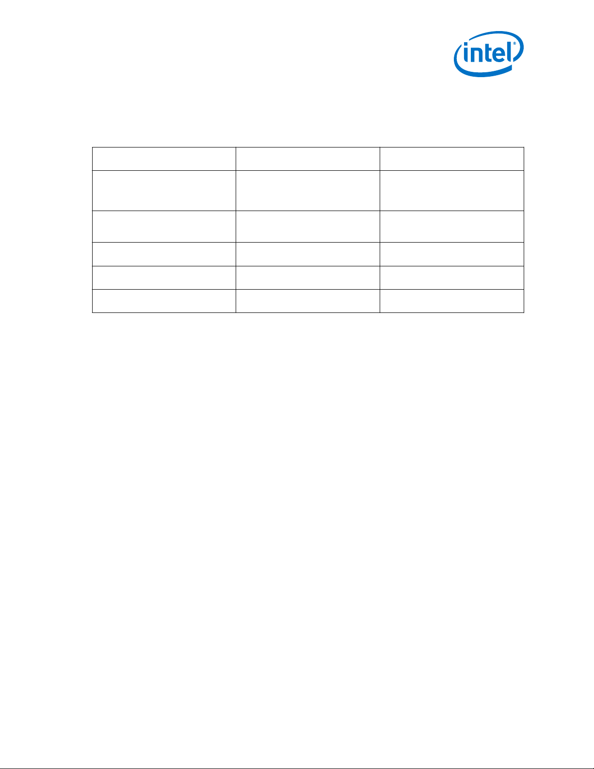
Table 1. The SoC FPGA Designer's Checklist
Step Title Links Check (X)
HPS Designer's Checklist for SoC FPGAs
Start your SoC FPGA Design here Start your SoC-FPGA design here on page 15
Determining your SoC FPGA Topology on page 15
Design Considerations for Connecting
Device I/O to HPS Peripherals and
Memory
HPS Clocking and Reset Design
Considerations
HPS EMIF Design Considerations Considerations for Connecting HPS to SDRAM on page 21
DMA Considerations Choosing a DMA Controller on page 24
Managing Coherency for FPGA
Accelerators
IP Debug Tools IP Debug Tools on page 26
HPS Power Design Considerations Early System and Board Planning on page 33
Boundary Scan for HPS Boundary Scan for HPS on page 36
Design Guidelines for HPS Interfaces HPS EMAC PHY Interfaces on page 36
HPS Pin Assignment Design Considerations on page 17
HPS I/O Settings: Constraints and Drive Strengths on page 18
HPS Clock Planning on page 20
Early Pin Planning and I/O Assignment Analysis on page 20
Pin Features and Connections for HPS JTAG, Clocks, Reset and PoR
on page 20
Internal Clocks on page 21
HPS SDRAM I/O Locations on page 23
Integrating the HPS EMIF with the SoC FPGA Device on page 23
HPS Memory Debug on page 23
Optimizing DMA Master Bandwidth through HPS Interconnect on page
24
Timing Closure for FPGA Accelerators on page 24
Cache Coherency on page 25
Coherency between FPGA Logic and HPS: Accelerator Coherency Port
(ACP) on page 25
Data Size Impacts ACP Performance on page 25
FPGA Access to ACP via AXI or Avalon-MM on page 26
Data Alignment for ACP and L2 Cache ECC accesses on page 26
Board Designer's Checklist for SoC FPGAs
Early Power Estimation on page 33
Design Considerations for HPS and FPGA Power Supplies for SoC
FPGA devices on page 34
Pin Connection Considerations for Board Designs on page 34
Device Power-Up on page 34
Power Analysis and Optimization on page 35
continued...
AN 796: Cyclone V and Arria V SoC Device Design Guidelines
5
Page 6
1. Overview of the Design Guidelines for Cyclone® V SoC FPGAs and Arria® V SoC FPGAs
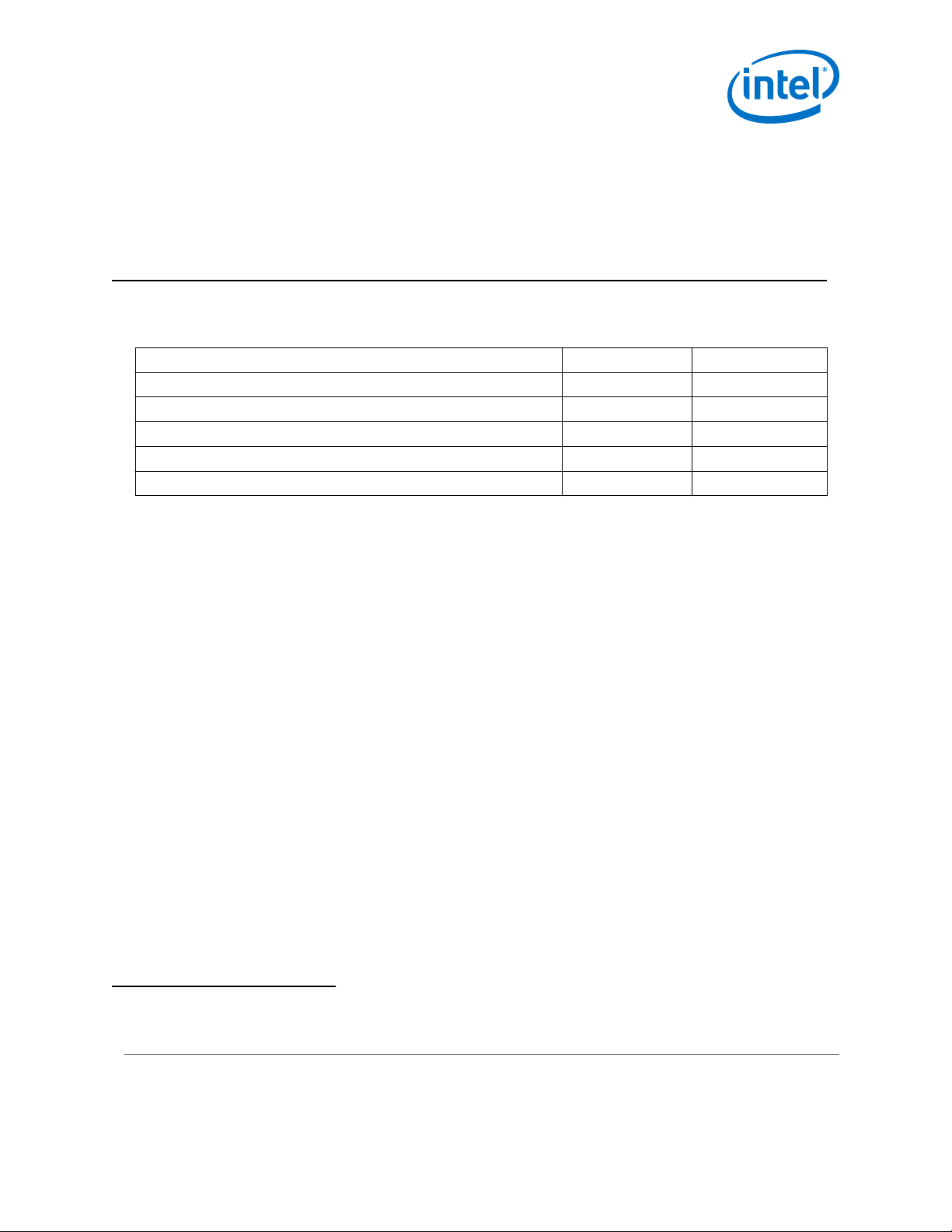
Step Title Links Check (X)
USB Interface Design Guidelines on page 43
QSPI Flash Interface Design Guidelines on page 44
SD/MMC and eMMC Card Interface Design Guidelines on page 45
NAND Flash Interface Design Guidelines on page 46
UART Interface Design Guidelines on page 46
I2C Interface Design Guidelines on page 47
SPI Interface Design Guidelines on page 47
Embedded Software Designer's Checklist for SoC FPGAs
Assemble the components of your
Software Development Platform
Select an Operating System (OS) for
your application
Assemble your Software
Development Platform for Linux
Assemble your Software
Development Platform for Bare-metal
Application
Assemble your Software
Development Platform for Partner
OS/RTOS Application
Choose the Boot Loader Software Choosing Boot Loader Software on page 58
Selecting Software Tools for
Development, Debug and Trace
Board Bring Up Considerations Board Bring Up Considerations on page 28
Boot and Configuration Design
Considerations
Flash Device Driver Considerations Flash Device Driver Design Considerations on page 61
HPS ECC Design Considerations HPS ECC Design Considerations on page 61
HPS SDRAM Considerations HPS SDRAM Considerations on page 63
Assembling the Components of Your Software Development Platform
on page 49
Golden Hardware Reference Design on page 50
Linux or RTOS on page 52
Bare Metal on page 52
Using Symmetrical vs. Asymmetrical Multiprocessing (SMP vs. AMP)
Modes on page 53
Golden System Reference Design (GSRD) for Linux on page 54
GSRD for Linux Development Flow on page 54
GSRD for Linux Build Flow on page 55
Linux Device Tree Design Considerations on page 56
Assembling a Software Development Platform for a Bare-Metal
Application on page 57
Assembling your Software Development Platform for a Partner OS or
RTOS on page 58
Select Software Build Tools on page 60
Select Software Debug Tools on page 60
Select Software Trace Tools on page 61
Boot Design Considerations on page 28
Configuration on page 32
AN-796 | 2018.06.18
AN 796: Cyclone V and Arria V SoC Device Design Guidelines
6
Page 7
1. Overview of the Design Guidelines for Cyclone® V SoC FPGAs and Arria® V SoC FPGAs
AN-796 | 2018.06.18
1.2. Overview of HPS Design Guidelines for SoC FPGA design
Table 2. HPS Design Guidelines Overview
Stages of the HPS Design Flow Guidelines Links
Hardware and Software Partitioning Determine your system topology and
HPS Pin Multiplexing and I/O
Configuration Settings
HPS Clocks and Reset Considerations HPS clocks and cold and warm reset
HPS EMIF Considerations Usage of the HPS EMIF controller and
FPGA Accelerator Design
Considerations
Recommended Tools for IP
Development
use it as a starting point for your HPS
to FPGA interface design.
Plan configuration settings for the HPS
system including I/O multiplexing
options, interface to FPGA and SDRAM,
clocks, peripheral settings
considerations
related considerations
Design considerations to manage
coherency between FPGA accelerators
and the HPS
Signal Tap II, BFMs, System Console IP Debug Tools on page 26
Guidelines for Interconnecting the HPS
and FPGA on page 10
Design Considerations for Connecting
Device I/O to HPS Peripherals and
Memory on page 16
HPS Clocking and Reset Design
Considerations on page 19
HPS EMIF Design Considerations on
page 21
DMA Considerations on page 24
AN 796: Cyclone V and Arria V SoC Device Design Guidelines
7
Page 8
1. Overview of the Design Guidelines for Cyclone® V SoC FPGAs and Arria® V SoC FPGAs
AN-796 | 2018.06.18
1.3. Overview of Board Design Guidelines for SoC FPGA Design
Table 3. Board Design: Design Guidelines Overview
Stages of the Board Design Flow Guidelines Links
HPS Power design considerations Power on board bring up, early power
Board design guidelines for HPS
interfaces
estimation, design considerations for
HPS and FPGA power supplies, power
analysis and power optimization
Includes EMAC, USB, QSPI, SD/MMC,
NAND, UART and I2C
HPS Power Design Considerations on
page 32
Design Guidelines for HPS Interfaces
on page 36
AN 796: Cyclone V and Arria V SoC Device Design Guidelines
8
Page 9
1. Overview of the Design Guidelines for Cyclone® V SoC FPGAs and Arria® V SoC FPGAs
AN-796 | 2018.06.18
1.4. Overview of Embedded Software Design Guidelines for SoC FPGA Design
Table 4. Embedded Software: Design Guidelines Overview
Stages of the Embedded Software
Operating System (OS) considerations OS considerations to meet your
Boot Loader considerations Boot loader considerations to meet
Boot and Configuration Design
Considerations
HPS ECC Considerations ECC for external SDRAM interface, L2
HPS SDRAM Considerations Using Preloader to debug HPS SDRAM,
Design Flow
application needs, including real time,
software reuse, support and ease of
use considerations
your application needs. including GPL
requirements, and features.
Boot source, boot clock, boot fuses,
configuration flows
cache data memory, flash memory
Accessing the HPS SDRAM
Guidelines Links
Selecting an Operating System for Your
Application on page 52
Choosing Boot Loader Software on
page 58
Boot and Configuration Design
Considerations on page 28
HPS ECC Design Considerations on
page 61
HPS SDRAM Considerations on page
63
AN 796: Cyclone V and Arria V SoC Device Design Guidelines
9
Page 10
AN-796 | 2018.06.18
2. Background: Comparison between Cyclone V SoC FPGA and Arria V SoC FPGA HPS Subsystems
While the HPS subsystems in Cyclone V SoC and Arria V SoC are architecturally
similar, there are a few differences in features as listed below.
HPS Features
Maximum MPU Frequency Up to 925 MHz Up to 1.05 GHz
Controller Area Network (CAN) Yes No
Total HPS Dedicated I/O with Loaner capability Up to 67 94
Automotive Grade Option Yes No
Maximum supported DDR3 Frequency for HPS SDRAM 400 MHz 533 MHz
Cyclone V SoC Arria V SoC
Related Information
Differences Among Intel SoC Device Families
2.1. Guidelines for Interconnecting the HPS and FPGA
The memory-mapped connectivity between the HPS and the FPGA fabric is a crucial
tool to maximize the performance of your design.
Design guidelines for the FPGA portion of your design are provided in the Arria V and
Cyclone V Design Guidelines.
Related Information
Arria V and Cyclone V Design Guidelines
2.1.1. HPS-FPGA Bridges
(1)
The HPS has three bridges that use memory-mapped interfaces to the FPGA based on
the Arm* Advanced Microcontroller Bus Architecture (AMBA*) Advanced eXtensible
Interface (AXI*). Their purpose determines the direction of each bridge.
(1)
You can only assign a maximum of 71 HPS I/O as Loaner I/O to the FPGA. For a detailed
comparison between the HPS subsystem for Cyclone V SoC and Arria V SoC, refer to
Differences Among Intel SoC Device Families.
Intel Corporation. All rights reserved. Intel, the Intel logo, Altera, Arria, Cyclone, Enpirion, MAX, Nios, Quartus
and Stratix words and logos are trademarks of Intel Corporation or its subsidiaries in the U.S. and/or other
countries. Intel warrants performance of its FPGA and semiconductor products to current specifications in
accordance with Intel's standard warranty, but reserves the right to make changes to any products and services
at any time without notice. Intel assumes no responsibility or liability arising out of the application or use of any
information, product, or service described herein except as expressly agreed to in writing by Intel. Intel
customers are advised to obtain the latest version of device specifications before relying on any published
information and before placing orders for products or services.
*Other names and brands may be claimed as the property of others.
ISO
9001:2015
Registered
Page 11
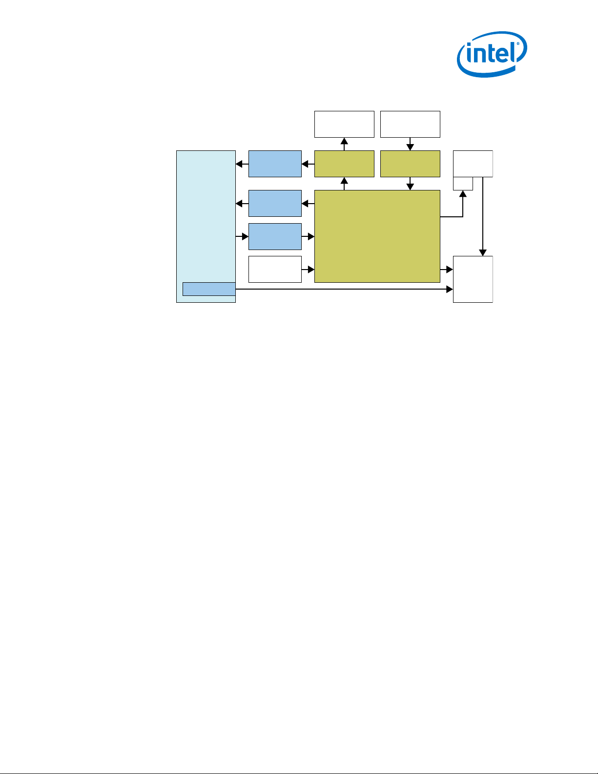
LWH2F Bridge
32 bit
H2F Bridge
32/64/128 bit
F2H Bridge
32/64/128 bit
DMA
L3 Slave
Peripheral Switch
All Other
L3 Slaves
L3 Master
Peripheral Switch
All Other
L3 Masters
L3 Interconnect
Main Switch
FPGA Fabric
F2S Interface
MPU
SRAM
Controller
ACP
Key:
H2F: HPS-to-FPGA
LWH2F: Lightweight HPS-to-FPGA
F2H: FPGA-to-HPS
F2S: FPGA-to-SDRAM
2. Background: Comparison between Cyclone V SoC FPGA and Arria V SoC FPGA HPS Subsystems
AN-796 | 2018.06.18
Figure 1. HPS-FPGA Bridges
2.1.1.1. Lightweight HPS-to-FPGA Bridge
GUIDELINE: Use the lightweight HPS-to-FPGA bridge to connect IP that
needs to be controlled by the HPS.
The lightweight HPS-to-FPGA bridge allows masters in the HPS to access memorymapped control slave ports in the FPGA portion of the SoC device. Typically, only the
MPU inside the HPS accesses this bridge to perform control and status register
accesses to peripherals in the FPGA.
GUIDELINE: Do not use the lightweight HPS-to-FPGA bridge for FPGA
memory. Instead use the HPS-to-FPGA bridge for memory.
When the MPU accesses control and status registers within peripherals, these
transactions are typically strongly ordered (non-posted). By dedicating the lightweight
HPS-to-FPGA bridge to register accesses, the access time is minimized because
bursting traffic is routed to the HPS-to-FPGA bridge instead.
The lightweight HPS-to-FPGA bridge has a fixed 32-bit width connection to the FPGA
fabric, because most IP cores implement 32-bit control and status registers. However,
Platform Designer (Standard) can adapt the transactions to widths other than 32 bits
within the FPGA-generated network interconnect.
AN 796: Cyclone V and Arria V SoC Device Design Guidelines
11
Page 12

2. Background: Comparison between Cyclone V SoC FPGA and Arria V SoC FPGA HPS Subsystems
2.1.1.2. HPS-to-FPGA Bridge
GUIDELINE: Use the HPS-to-FPGA bridge to connect memory hosted by the
FPGA to the HPS.
The HPS-to-FPGA bridge allows masters in the HPS such as the microprocessor unit
(MPU), DMA, or peripherals with integrated masters to access memory hosted by the
FPGA portion of the SoC device. This bridge supports 32, 64, and 128-bit datapaths,
allowing the width to be tuned to the largest slave data width in the FPGA fabric
connected to the bridge. This bridge is intended to be used by masters performing
bursting transfers and should not be used for accessing peripheral registers in the
FPGA fabric. Control and status register accesses should be sent to the lightweight
HPS-to-FPGA bridge instead.
GUIDELINE: If memory connected to the HPS-to-FPGA bridge is used for HPS
boot, ensure that its slave address is set to 0x0 in Platform Designer
(Standard).
When the HPS BSEL pins are set to boot from FPGA (BSEL = 1) the processor
executes code hosted by the FPGA residing at offset 0x0 from the HPS-to-FPGA
bridge. This is the only bridge that can be used for hosting code at boot time.
2.1.1.3. FPGA-to-HPS Bridge
AN-796 | 2018.06.18
GUIDELINE: Use the FPGA-to-HPS bridge for cacheable accesses to the HPS
from masters in the FPGA.
The FPGA-to-HPS bridge allows masters implemented in the FPGA fabric to access
memory and peripherals inside the HPS. This bridge supports 32, 64, and 128-bit
datapaths so that you can adjust it to be as wide as the widest master implemented in
the FPGA.
GUIDELINE: Use the FPGA-to-HPS bridge to access cache-coherent memory,
peripherals, or on-chip RAM in the HPS from masters in the FPGA.
Although this bridge has direct connectivity to the SDRAM subsystem, the main intent
of the bridge is to provide access to peripherals and on-chip memory, as well as
provide cache coherency with connectivity to the MPU accelerator coherency port
(ACP).
To access the HPS SDRAM directly without coherency you should connect masters in
the FPGA to the FPGA-to-SDRAM ports instead, because they provide much more
bandwidth and lower-latency access.
2.1.2. FPGA-to-HPS SDRAM Access
In addition to the FPGA-to-HPS bridge, FPGA logic can also use the FPGA-to-SDRAM
interface to access the HPS SDRAM.
GUIDELINE: Use the FPGA-to-SDRAM ports for non-cacheable access to the
HPS SDRAM from masters in the FPGA.
The FPGA-to-SDRAM ports allow masters implemented in the FPGA fabric to directly
access HPS SDRAM without the transactions flowing through the L3 interconnect.
AN 796: Cyclone V and Arria V SoC Device Design Guidelines
12
Page 13
2. Background: Comparison between Cyclone V SoC FPGA and Arria V SoC FPGA HPS Subsystems
AN-796 | 2018.06.18
These interfaces connect only to the HPS SDRAM subsystem so it is recommended to
use them in your design if the FPGA needs high-throughput, low-latency access to the
HPS SDRAM. The exception to this recommendation is if the FPGA requires cache
coherent access to SDRAM.
The FPGA-to-SDRAM interfaces cannot access the MPU ACP slave; so if you require a
master implemented in the FPGA to access cache coherent data, ensure that it is
connected to the FPGA-to-HPS bridge instead.
The FPGA-to-SDRAM interface has three port types that are used to create the AXI
and Avalon-MM interfaces:
• Command ports—issue read and/or write commands, and for receive write
acknowledge responses
• 64-bit read data ports—receive data returned from a memory read
• 64-bit write data ports—transmit write data
There is a maximum of six command ports, four 64-bit read data port and four 64-bit
write data port. The table below shows the possible port utilization.
Table 5. FPGA-to-HPS SDRAM Port Utilization
Bus Protocol Command Ports Read Data Ports Write Data Ports
32- or 64-bit AXI 2 1 1
128-bit AXI 2 2 2
256-bit AXI 2 4 4
32- or 64-bit Avalon-MM 1 1 1
128-bit Avalon-MM 1 2 2
256-bit Avalon-MM 1 4 4
32- or 64-bit Avalon-MM write-only 1 0 1
128-bit Avalon-MM write-only 1 0 2
256-bit Avalon-MM write-only 1 0 4
32- or 64-bit Avalon-MM read-only 1 1 0
128-bit Avalon-MM read-only 1 2 0
256-bit Avalon-MM read-only 1 4 0
For more information about the FPGA-to-HPS SDRAM interface, refer to the "SDRAM
Controller Subsystem" chapter of the Cyclone V or Arria V SoC Hard Processor System
Technical Reference Manual.
Note: To access the HPS SDRAM via the FPGA-to-SDRAM interface, follow the guidelines in
Access HPS SDRAM via the FPGA-to-SDRAM Interface on page 67.
Related Information
• SDRAM Controller Subsystem - Cyclone V Hard Processor System Technical
Reference Manual
• SDRAM Controller Subsystem - Arria V Hard Processor System Technical Reference
Manual
AN 796: Cyclone V and Arria V SoC Device Design Guidelines
13
Page 14

2. Background: Comparison between Cyclone V SoC FPGA and Arria V SoC FPGA HPS Subsystems
AN-796 | 2018.06.18
2.1.3. Connecting Soft Logic to HPS Component
Designers can connect soft logic components to the HPS using the Cyclone V/Arria V
HPS component in Platform Designer (Standard).
Note: Refer to the "Introduction to the HPS Component" and "Instantiating the HPS
Component" chapters of the appropriate Hard Processor System Technical Reference
Manual to understand the interface and available options. To connect a FPGA soft IP
component to the HPS, Platform Designer (Standard) provides the component editor
tool. For more information, refer to the "Creating Platform Designer (Standard)
Components" chapter of the Intel® Quartus® Prime Standard Edition Handbook,
Volume 1: Design and Synthesis.
Note: When designing and configuring high bandwidth DMA masters and related buffering in
the FPGA core, refer to the DMA Considerations on page 24 section of this document.
The principles covered in that section apply to all high bandwidth DMA masters (for
example Platform Designer (Standard) DMA Controller components, integrated DMA
controllers in custom peripherals) and related buffering in the FPGA core that access
HPS resources (for example HPS SDRAM) through the FPGA-to-SDRAM and FPGA-toHPS bridge ports, not just tightly coupled Arm CPU accelerators.
Related Information
• Introduction to the HPS Component - Cyclone V Hard Processor System Technical
Reference Manual
• Instantiating the HPS Component - Cyclone V Hard Processor System Technical
Reference Manual
• Introduction to the HPS Component - Arria V Hard Processor System Technical
Reference Manual
• Instantiating the HPS Component - Arria V Hard Processor System Technical
Reference Manual
AN 796: Cyclone V and Arria V SoC Device Design Guidelines
14
Page 15

AN-796 | 2018.06.18
3. Design Guidelines for HPS portion of SoC FPGAs
3.1. Start your SoC-FPGA design here
3.1.1. Recommended Starting Point for HPS-to-FPGA Interface Design
Depending on your topology, you can choose one of the two hardware reference
designs as a starting point for your hardware design.
GUIDELINE: Use the Golden System Reference Design (GSRD) as a starting
point for a loosely coupled system.
The Golden Hardware Reference Design (GHRD) has the optimum default settings and
timing that you can use as a basis for your "getting started" system. After initial
evaluation, you can move on to the Cyclone V HPS-to-FPGA Bridge Design Example
reference design to compare performance among the various FPGA-HPS interfaces.
Refer to "Golden Hardware Reference Design" for more information.
GUIDELINE: Use the Cyclone V HPS-to-FPGA Bridge Design Example
reference design to determine your optimum burst length and data-width for
accesses between FPGA logic and HPS.
The Cyclone V FPGA-to-HPS bridge design example contains modular SGDMAs in the
FPGA logic that allow you to program the burst length for data accesses from the FPGA
logic to the HPS.
Related Information
Golden Hardware Reference Design on page 50
3.1.2. Determining your SoC FPGA Topology
To determine which system topology best suits your application, you must first
determine how to partition your application into hardware and software.
GUIDELINE: Profile your software to identify functions for hardware
acceleration.
Use any good profiling tool (such as DS-5 streamline profiler) to identify functions that
are good candidates for hardware acceleration, and isolate functions that are best
implemented in software.
Intel Corporation. All rights reserved. Intel, the Intel logo, Altera, Arria, Cyclone, Enpirion, MAX, Nios, Quartus
and Stratix words and logos are trademarks of Intel Corporation or its subsidiaries in the U.S. and/or other
countries. Intel warrants performance of its FPGA and semiconductor products to current specifications in
accordance with Intel's standard warranty, but reserves the right to make changes to any products and services
at any time without notice. Intel assumes no responsibility or liability arising out of the application or use of any
information, product, or service described herein except as expressly agreed to in writing by Intel. Intel
customers are advised to obtain the latest version of device specifications before relying on any published
information and before placing orders for products or services.
*Other names and brands may be claimed as the property of others.
ISO
9001:2015
Registered
Page 16
Bank 8A HPS Column I/O
Bank 3B Bank 4ABank 3A
Bank 5B HPS Row I/OBank 5A
Transceiver Block
HPS Core
3. Design Guidelines for HPS portion of SoC FPGAs
AN-796 | 2018.06.18
3.2. Design Considerations for Connecting Device I/O to HPS Peripherals and Memory
One of the most important considerations when configuring the HPS is to understand
how the I/O is organized in the Cyclone V/Arria V SoC devices. The HPS I/O is
physically divided into:
• HPS Column I/O: Contains the HPS Dedicated Function Pins and HPS Dedicated
I/O with loaner capability
• HPS Row I/O: Contains the HPS External Memory Interface (EMIF) I/O and HPS
General Purpose Input (GPI) pins
Figure 2. Example layout for HPS Column I/O and HPS Row I/O in Cyclone V SX and ST
device
Note: For more information regarding the I/O pin layout, refer to the appropriate "I/O
Features" chapter in the Cyclone V or Arria V Device Handbook, Volume 1: Device
Interfaces and Integration.
Table 6. HPS I/O Pin Type Summary
Pin Type Purpose
HPS Dedicated Function Pins Each I/O has only one function and cannot be used for other purposes.
HPS Dedicated I/O with loaner
capability
HPS External Memory Interface (EMIF)
I/O
HPS General Purpose Input (GPI) Pins These pins are also known as HLGPI pins. These input-only pins are located in
FPGA I/O These are general purpose I/O that can be used for FPGA logic and FPGA
These I/Os are primarily used by the HPS, but can be used on an individual basis
by the FPGA if the HPS is not using them.
These I/Os are used for connecting to the HPS external memory interface
(EMIF). Refer to the "External Memory Interface in Cyclone V Devices" or
"External Memory Interface in Arria V Devices" chapter in the respective device
handbook for more information regarding the layout of these I/O pins.
the same bank as the HPS EMIF I/O. Note that the smallest Cyclone V SoC
package U19 (484 pins) does not have any HPS GPI pins.
External Memory Interfaces.
AN 796: Cyclone V and Arria V SoC Device Design Guidelines
16
Page 17
3. Design Guidelines for HPS portion of SoC FPGAs
AN-796 | 2018.06.18
The table below summarizes the characteristics of each I/O type.
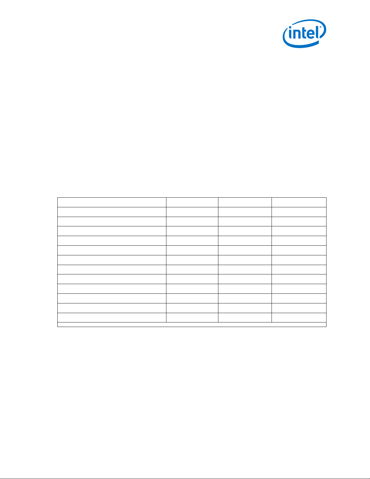
Table 7. I/O Types
HPS Dedicated
Function Pins
Number of Available I/O 11 Up to 67
Voltages Supported 3.3V, 3.0V,
2.5V, 1.8V,
1.5V
Purpose Clock, Reset,
HPS JTAG
Timing Constraints Fixed Fixed Fixed for legal
Recommended Peripherals JTAG QSPI, NANDx8,
HPS Dedicated
I/O with
loaner
capability
(Cyclone V
SoC) and 94
(Arria V SoC)
3.3V, 3.0V,
2.5V, 1.8V,
1.5V
Boot source,
High speed
HPS
peripherals
eMMC, SD/
MMC, UART,
USB, EMAC
HPS External
Memory
Interface
Up to 86 14 (except for
LVDS I/O for
DDR3, DDR2
and LPDDR2
protocols
Connect to
SDRAM
combinations
DDR3, DDR2
and LPDDR2
SDRAM
HPS General
Purpose Input
Cyclone V SoC
U19 package )
Same as the
I/O bank
voltage used
for HPS EMIF
General
Purpose Input
Fixed User defined
GPI Slow speed
FPGA I/O
Up to 288
(Cyclone V
SoC) and Up to
592 (Arria V
SoC)
3.3V, 3.0V,
2.5V, 1.8V,
1.5V, 1.2V
General
Purpose I/O
peripherals
(I2C, SPI,
EMAC-MII)
Note: You can access the timing information to perform off-chip analysis by reviewing the
HPS timing in the Cyclone V Device Datasheet or Arria V Device Datasheet.
Related Information
• I/O Features in Cyclone V Devices
Chapter in the Cyclone V Device Handbook, Volume 1: Device Interfaces and
Integration
• I/O Features in Arria V Devices
Chapter in the Arria V Device Handbook, Volume 1: Device Interfaces and
Integration
3.2.1. HPS Pin Assignment Design Considerations
Because the HPS contains more peripherals than can all be connected to the HPS
Dedicated I/O, the HPS component in Platform Designer (Standard) offers pin
multiplexing settings as well as the option to route most of the peripherals into the
FPGA fabric. Any unused pins for the HPS Dedicated I/O with loaner capability
meanwhile can be used as general purpose I/O by the FPGA.
Note that a HPS I/O Bank can only support a single supply of either 1.2V, 1.35V, 1.5V,
1.8V, 2.5V, 3.0V, or 3.3V power supply, depending on the I/O standard required by the
specified bank. 1.35V is supported for HPS Row I/O bank only.
AN 796: Cyclone V and Arria V SoC Device Design Guidelines
17
Page 18

3. Design Guidelines for HPS portion of SoC FPGAs
AN-796 | 2018.06.18
GUIDELINE: Ensure that you route USB, EMAC and Flash interfaces to HPS
Dedicated I/O first, starting with USB.
It is recommended that you start by routing high speed interfaces such as USB,
Ethernet, and flash to the HPS Dedicated I/O first. USB must be routed to HPS
Dedicated I/O because it is not available to the FPGA fabric. The flash boot source
must also be routed to the HPS dedicated I/O (and not any FPGA I/O) since these are
the only I/Os that are functional before the FPGA I/Os have been configured.
Note: For Cyclone V SoC U19 package (484 pin count) only one USB controller (instead of
two) is usable due to reduced number of available HPS I/O. For more information,
refer to Why can't I map USB0 to HPS IO in my Cyclone V SoC U19 package (484 pin
count)? in the Knowledge Base.
GUIDELINE: Enable the HPS GPI pins in the Platform Designer (Standard)
HPS Component if needed
By default, the HPS GPI interface is not enabled in Platform Designer (Standard). To
enable this interface, you must select the checkbox "Enable HLGPI interface" in the
Platform Designer (Standard) HPS Component for Cyclone V/Arria V. These pins are
then exposed as part of the Platform Designer (Standard) HPS Component Conduit
Interface and can be individually assigned at the top level of the design.
3.2.2. HPS I/O Settings: Constraints and Drive Strengths
GUIDELINE: Ensure that you have I/O settings for the HPS Dedicated I/O
(drive strength, I/O standard, weak pull-up enable, etc.)
The HPS pin location assignments are managed automatically when you generate the
Platform Designer (Standard) system containing the HPS. As for the HPS SDRAM, the
I/O standard and termination settings are done once you run the
“hps_sdram_p0_pin_assignments.tcl” script that is created once the Platform
Designer (Standard) HPS Component has been generated.
Note:
You can locate the script “hps_sdram_p0_pin_assignments.tcl” in the following
directory once the Platform Designer (Standard) HPS Component has been generated:
<Quartus project directory>\<Platform Designer (Standard) file
name>\synthesis\submodule. Shown below is an example of selecting the script in
Intel Quartus Prime.
AN 796: Cyclone V and Arria V SoC Device Design Guidelines
18
Page 19
3. Design Guidelines for HPS portion of SoC FPGAs
AN-796 | 2018.06.18
The only HPS I/O constraints you must manage are for HPS Dedicated Function Pins
and HPS Dedicated I/O. Constraints such as drive strength, I/O standards, and weak
pull-up enables are added to the Intel Quartus Prime project just like FPGA constraints
and are applied to the HPS at boot time when the second stage bootloader configures
the I/O. For FPGA I/O, the I/O constraints are applied to the FPGA configuration file.
Note: During power up, the HPS Dedicated I/O required for boot flash devices are configured
by the Boot ROM, depending on the BSEL values.
3.3. HPS Clocking and Reset Design Considerations
The main clock and resets for the HPS subsystem are HPS_CLK1, HPS_CLK2,
HPS_nPOR, HPS_nRST and HPS_PORSEL. HPS_CLK1 sources the Main PLL that
generates the clocks for the MPU, L3/L4 sub-systems, debug sub-system and the
Flash controllers. It can also be programmed to drive the Peripheral and SDRAM PLLs.
HPS_CLK2 meanwhile can be used as an alternative clock source to the Peripheral and
the SDRAM PLLs.
HPS_nPOR provides a cold reset input, and HPS_nRST provides a bidirectional warm
reset resource. As for the HPS_PORSEL, it is an input pin that can be used to select
either a standard POR delay or a fast POR delay for the HPS block.
Note: Refer to the Cyclone V Device Family Pin Connection Guidelines or Arria V GT, GX, ST,
and SX Device Family Pin Connection Guidelines for more information on connecting
the HPS clock and reset pins.
AN 796: Cyclone V and Arria V SoC Device Design Guidelines
19
Page 20

3. Design Guidelines for HPS portion of SoC FPGAs
3.3.1. HPS Clock Planning
GUIDELINE: Verify MPU and peripheral clocking using Platform Designer
(Standard)
Use Platform Designer (Standard) to initially define your HPS component
configuration. Set the HPS input clocks, and peripheral source clocks and frequencies.
Note any Platform Designer (Standard) warning or error messages. You can address
them by modifying clock settings. In some cases you might determine that a
particular warning condition does not impact your application.
3.3.2. Early Pin Planning and I/O Assignment Analysis
GUIDELINE: Choose an I/O voltage level for the HPS Dedicated Function I/O
HPS_CLK1, HPS_CLK2, HPS_nPOR and HPS_nRST are powered by
VCCRSTCLK_HPS. These HPS Dedicated Function Pins are LVCMOS/LVTTL at either
3.3V, 3.0V, 2.5V or 1.8V. The I/O signaling voltage for these pins are determined by
the supply level applied to VCCRSTCLK_HPS.
AN-796 | 2018.06.18
Note:
HPS_PORSEL can be connected to either VCCRSTCLK_HPS (for fast HPS POR delay) or
GND (for standard HPS POR delay).
Note:
VCCRSTCLK_HPS can share the same power and regulator with VCCIO_HPS and
VCCPD_HPS if they share the same voltage requirement. The functionality of powering
down the FPGA fabric, while keeping the HPS running, is not needed.
3.3.3. Pin Features and Connections for HPS JTAG, Clocks, Reset and PoR
GUIDELINE: With the HPS in use (powered), supply a free running clock on
HPS_CLK1 for SoC device HPS JTAG access.
Access to the HPS JTAG requires an active clock source driving HPS_CLK1.
GUIDELINE: When daisy chaining the FPGA and HPS JTAG for a single device,
ensure that the HPS JTAG is first device in the chain (located before the FPGA
JTAG).
Placing the HPS JTAG before the FPGA JTAG allows the ARM DS-5 debugger to initiate
warm reset to the HPS. However, in case of cold reset the entire JTAG chain is broken
until the cold reset completes, as discussed in the next section.
GUIDELINE: Consider board design to isolate HPS JTAG interface
The HPS Test Access Port (TAP) controller is reset on a cold reset. If the HPS JTAG and
FPGA JTAG are daisy-chained together, the entire JTAG chain is broken until the cold
reset completes. If access to the JTAG chain is required during HPS cold reset, design
the board to allow HPS JTAG to be bypassed.
GUIDELINE: HPS_nRST is an open-drain, bidirectional dedicated warm reset
I/O.
HPS_nRST is an active low, open-drain-type, bidirectional I/O. Externally asserting a
logic low to the HPS_nRST pin initiates a warm reset of the HPS subsystem. HPS warm
and cold reset can also be asserted from internal sources such as software-initiated
AN 796: Cyclone V and Arria V SoC Device Design Guidelines
20
Page 21

3. Design Guidelines for HPS portion of SoC FPGAs
AN-796 | 2018.06.18
resets and reset requests from the FPGA fabric. When the HPS is internally placed in a
warm reset state, the HPS component becomes a reset source and drives the
HPS_nRST pin low, resetting any connected board-level components.
GUIDELINE: Observe the minimum assertion time specifications of HPS_nPOR
and HPS_nRST.
Reset signals on the HPS_nPOR and HPS_nRST pins must be asserted for a minimum
number of HPS_CLK1 cycles as specified in the HPS section of the Cyclone V Device
Datasheet or Arria V Device Datasheet.
3.3.4. Internal Clocks
GUIDELINE: Avoid cascading PLLs between the HPS and FPGA
Cascading PLLs between the FPGA and HPS has not been characterized. Unless you
perform the jitter analysis, do not chain the FPGA and HPS PLLs together as a stable
clock coming out of the last PLL in the FPGA cannot be guaranteed. Output clocks from
the HPS are not intended to be fed into PLLs in the FPGA.
3.4. HPS EMIF Design Considerations
A critical component of the HPS subsystem is the external SDRAM memory. For
Cyclone V and Arria V SoC device, the HPS has a dedicated SDRAM Subsystem that
interfaces with the HPS External Memory Interface I/O.
Review the following guidelines to properly design the interface between the memory
and the HPS. These guidelines are essential to successfully connecting external
SDRAM to the HPS.
The External Memory Interface Handbook, Volume 3: Reference Material includes the
functional description of the HPS memory controller. The supported interface options
are listed for DDR3, DDR2 and LPDDR2.
3.4.1. Considerations for Connecting HPS to SDRAM
GUIDELINE: Ensure that the HPS memory controller Data Mask (DM) pins are
enabled
In the HPS Component in Platform Designer (Standard), ensure that the checkbox to
enable the data mask pins is enabled. If this control is not enabled, data corruption
occurs any time a master accesses data in SDRAM that is smaller than the native word
size of the memory.
AN 796: Cyclone V and Arria V SoC Device Design Guidelines
21
Page 22
3. Design Guidelines for HPS portion of SoC FPGAs
Figure 3. Setting the Enable DM Pins Option in HPS Component
AN-796 | 2018.06.18
Determine your SDRAM Memory type and bit width. Cyclone V and Arria V SoC devices
offer DDR3, DDR2 and LPDDR2 SDRAM support for the HPS.
GUIDELINE: Ensure that you choose only DDR3, DDR2, or LPDDR2
components or modules in configurations supported by the Cyclone V or Arria
V HPS EMIF for your specific device/package combination.
The External Memory Interface Spec Estimator, available on the External Memory
Interface page, is a parametric tool that allows you to compare supported external
memory interface types, configurations and maximum performance characteristics in
Intel FPGA and SoC devices.
First, filter the “Family” to select only Cyclone V /Arria V SoC device. Then, follow on
by using the filter on “Interface Type” to choose only “HPS Hard Controller”
GUIDELINE: Ensure that in the HPS Component, the Memory Clock Frequency
is supported by the device speed grade.
To obtain the maximum supported memory clock frequency for the device speed
grade, refer to the External Memory Interface Spec Estimator, available on the
External Memory Interface page.
AN 796: Cyclone V and Arria V SoC Device Design Guidelines
22
Page 23

3. Design Guidelines for HPS portion of SoC FPGAs
AN-796 | 2018.06.18
3.4.2. HPS SDRAM I/O Locations
The Cyclone V and Arria V SoC HPS External Memory Interface I/O locations are fixed,
depending on the type of memory used. You can refer to the device Pin Out files,
under the “HMC Pin Assignment for DDR3/DDR2” and “HMC Pin Assignment
for LPDDR2” for exact I/O pins used by the respective memory interface pins.
Note: Unused HPS External Memory Interface I/O Pins cannot be assigned to HPS
Peripherals, or used by the FPGA as Loaner IO.
Note: The smallest Cyclone V SoC package U19 (484 pin count) has narrower HPS SDRAM
width (32-bit) compared to larger packages (40-bit). Refer to the "External Memory
Interfaces in Cyclone V Devices" chapter in Cyclone V Device Handbook Volume 1:
Device Interfaces and Integration for more information.
Related Information
Documentation: Pin-Out Files for Intel FPGA Devices
3.4.3. Integrating the HPS EMIF with the SoC FPGA Device
Consider the following when integrating the Cyclone V or Arria V SoC HPS EMIF with
the rest of the SoC system design.
GUIDELINE: Follow the guidelines for optimizing bandwidth for all masters
accessing the HPS SDRAM
Accesses to SDRAM connected to the HPS EMIF go through the L3 Interconnect
(except for FPGA-to-SDRAM bridge). When designing and configuring high bandwidth
DMA masters and related buffering in the FPGA core, refer to DMA Considerations on
page 24. The principles covered in that section apply to all high bandwidth DMA
masters (for example DMA controller components, integrated DMA controllers in
custom peripherals) and related buffering in the FPGA core that access HPS resources
(for example HPS SDRAM) through the FPGA-to-SDRAM and FPGA-to-HPS bridge
ports, not just tightly-coupled HPS hardware accelerators.
3.4.4. HPS Memory Debug
The Cyclone V / Arria V HPS EMIF do not support the external memory interface
toolkit. To debug the HPS EMIF, you can change the settings inside the preloader
software to enable Runtime Calibration Report and Debug Level info. In addition, you
can use the preloader software to check the status of HPS SDRAM PLL.
Refer to Using the Preloader To Debug the HPS SDRAM on page 63 for more
information.
AN 796: Cyclone V and Arria V SoC Device Design Guidelines
23
Page 24

3. Design Guidelines for HPS portion of SoC FPGAs
AN-796 | 2018.06.18
3.5. DMA Considerations
3.5.1. Choosing a DMA Controller
Choose the DMA implementation best suited to your design
When DMA is required to improve system performance, you have the option to use the
DMA integrated into the HPS or a soft DMA module in the FPGA. When making the
choice of which option to use, you should consider the following:
• HPS DMA: primarily used to move data to and from other slow-speed HPS
modules, such as SPI and I2C, as well as to do memcopy functions to and from
HPS memories.
• Soft DMAs: primarily used to move data to and from peripherals in the FPGA.
3.5.2. Optimizing DMA Master Bandwidth through HPS Interconnect
FPGA DMA masters have access to HPS resources through the FPGA-to-HPS Bridge
and FPGA-to-SDRAM Interface, configurable in the HPS Platform Designer (Standard)
Component. The HPS SDRAM controller multi-port-front end (MPFE) provides
arbitration for these resources and enforce Quality of Service (QoS) settings. When
planning for and designing DMA masters and related buffering that access resources
through the HPS interconnect, study the architecture of the HPS interconnect and
consider the following guidance and resources available for optimizing bandwidth
through the interconnect.
GUIDELINE: Utilize the Cyclone V FPGA-to-HPS Bridge Design Example to
tune for performance
The Cyclone V FPGA-to-HPS Bridge Design Example is a useful platform for modeling
specific data traffic access patterns between the FPGA and HPS resources.
The example design includes a utility that can select the datapaths between
endpoints, select transaction characteristics (for example, burst lengths), and report
transfer bandwidth. This utility runs on the ARM Cortex* A-9 processor in the HPS.
3.5.3. Timing Closure for FPGA Accelerators
The HPS bridges and FPGA-to-SDRAM interfaces exposed to the FPGA are synchronous
and clock crossing is performed within the interface itself. As a result, you only need
to ensure that both the FPGA-facing logic and your user design close timing in Timing
Analyzer. Interrupts are considered asynchronous by the HPS, and as a result the HPS
logic resynchronizes them to the internal HPS clock domain so there is no need to
close timing for them.
Conduits carry signals that do not fit into any standard interface supported by
Platform Designer (Standard). Examples of these are HPS peripheral external
interfaces routed into the FPGA fabric or the HPS DMA peripheral request interfaces.
AN 796: Cyclone V and Arria V SoC Device Design Guidelines
24
Page 25

3. Design Guidelines for HPS portion of SoC FPGAs
AN-796 | 2018.06.18
3.6. Managing Coherency for FPGA Accelerators
Data shared between the HPS and the FPGA logic can be modified at any time, by
either the HPS or the FPGA. Many applications require data coherency, which means
that changes are propagated throughout the system, so that every master accesses
the most up-to-date data value.
When you design for data coherency, first you must determine which data transfers
need to be coherent. By default all access between the FPGA and HPS are assumed to
be non-coherent unless coherency is explicitly managed by software or using coherent
hardware features of the HPS (SCU and ACP).
To determine if peripherals in the FPGA need coherent access to HPS memory, answer
the follow questions:
• Does the MPU need to access data generated by my FPGA peripheral?
• Does the FPGA peripheral need to access data generated by the MPU?
If the answer to either question is "Yes", the data must be coherent. You can use the
ACP to keep the FPGA coherent with cacheable data in the HPS.
3.6.1. Cache Coherency
There are several mechanisms via which coherency are maintained through the
system:
The HPS maintains cache coherency at a level 1 memory subsystem level within the
MPU subsystem. The snoop control unit (SCU) built into the MPU subsystem maintains
cache coherency between the two L1 data caches using the modified-exclusiveshared-invalid (MESI) coherency protocol.
3.6.2. Coherency between FPGA Logic and HPS: Accelerator Coherency Port (ACP)
The accelerator coherency port (ACP) of the SCU provides a means for other masters
in the system, including logic implemented in the FPGA fabric, to perform cache
coherent accesses. Accesses to the ACP are only unidirectional in terms of cache
coherency meaning at the time of the access the data is up to date, but the SCU is not
responsible for maintaining coherency of that data over time. For example, if a master
in the FPGA reads data from the ACP and then a processor updates that same data in
memory, then the FPGA no longer contains the most up to date copy of the data.
3.6.3. Data Size Impacts ACP Performance
Performance explorations of accelerators using ACP show that as size of packets
transferred by AXI master via the ACP port increases the accelerator performance
increases but only up to a point. After that point, it is no longer possible to cache the
entire data packet, and the accelerator suffers performance degradation.
AN 796: Cyclone V and Arria V SoC Device Design Guidelines
25
Page 26

3. Design Guidelines for HPS portion of SoC FPGAs
GUIDELINE: Use ACP for managing coherency for small data size accesses,
manage coherency for large data in software.
3.6.4. FPGA Access to ACP via AXI or Avalon-MM
The AXI protocol allows masters to issue cacheable accesses whereas the Avalon-MM
protocol does not support this feature. For an FPGA master to perform a cacheable
access, the master must adhere to the AXI protocol and be able to perform cacheable
accesses, with ARCACHE[1] or AWCACHE[1] set to 1 and ARUSER[0] or AWUSER[0]
set to 1.
3.6.5. Data Alignment for ACP and L2 Cache ECC accesses
The L2 cache performs error detection and correction in groups of 64 bits without the
use of byte enables.
GUIDELINE: Accesses to the ACP must be 64-bit aligned, full 64-bit accesses,
and no byte lanes can disabled on write.
The main L3 switch and the ACP port are both 64 bits wide, so it is only necessary to
provide 64-bit aligned cache coherent accesses that are 64 bits wide after resizing.
Data resizing can occur in the L3 interconnect between requesting master and the
ACP. As a result, a 32-bit access can be compatible with the L2 cache ECC logic if the
access is aligned to 8-byte boundaries and the master performs bursts of size 2, 4, 8,
or 16. Data resizing can also occur within the FPGA-to-HPS bridge.
AN-796 | 2018.06.18
GUIDELINE: The simplest way to ensure that accesses from the FPGA meets
the L2 cache ECC requirements is to implement 64-bit masters in the FPGA
fabric and configure the FPGA-to-HPS bridge to expose a 64-bit slave port.
This ensures that no resizing of AXI transactions is necessary. Full 64-bit
accesses have to be made by the logic in the FPGA as well.
3.7. IP Debug Tools
The Intel Quartus Prime Design Software includes many IP and system-level debug
tools used in FPGA hardware designs.
The following tools are commonly used for system and IP debug in embedded
systems:
• Signal Tap - On-chip logic analyzer constructed from FPGA resources
• Bus functional models
— Avalon-MM v2 protocol
— AXI v3 protocol
• System console - Services-based API for controlling soft logic and moving data to/
from the FPGA
Each debug tool is introduced at different stages of the hardware design. In a typical
hardware design flow, the developer follows these high-level verification steps:
AN 796: Cyclone V and Arria V SoC Device Design Guidelines
26
Page 27

3. Design Guidelines for HPS portion of SoC FPGAs
AN-796 | 2018.06.18
1. IP Creation in RTL
2. Testbench and BFM verification of the IP
3. In silicon testing of the IP using system console to drive stimuli into memorymapped or streaming interface
4. In silicon testing of the IP using low level software run on the processor in the HPS
In the case of Signal Tap and system console, if both use the FPGA JTAG interface to
communicate data then they can be used simultaneously. For example, you may
instrument a trigger condition in Signal Tap and cause the trigger condition to occur
via the JTAG-to-Avalon bridge IP controlled by System console. These tools are also
capable of being used simultaneously with the HPS tools that communicate over JTAG.
There are two JTAG interfaces on the Cyclone V/Arria V SoC device. The first interface
is connected to the FPGA side of the device, while the second interface is connected to
the HPS debug access port (DAP).
Related Information
• "Design Debugging Using In-System Sources and Probes" chapter of the Intel
Quartus Prime Standard Edition Handbook Volume 3: Verification
Description of Signal Tap
• Avalon-MM v2 protocol
• AXI v3 protocol
• "System Debugging Tools Overview" chapter of the Intel Quartus Prime Standard
Edition Handbook Volume 3: Verification
Description of System Console
AN 796: Cyclone V and Arria V SoC Device Design Guidelines
27
Page 28

AN-796 | 2018.06.18
4. Board Design Guidelines for SoC FPGAs
4.1. Board Bring Up Considerations
This section describes the considerations that are useful for board bring up.
4.1.1. Reserved BSEL Setting
During initial stages of bring-up, if a JTAG connection cannot be established to the
target, it may be beneficial to set BSEL to 0x0 “Reserved” setting to prevent the
BootROM from trying to boot from a specific boot source. Then a test program could
be downloaded and ran with a debugger.
4.2. Boot and Configuration Design Considerations
4.2.1. Boot Design Considerations
4.2.1.1. Boot Source
GUIDELINE: Determine which boot source is to be supported.
The HPS side of the Cyclone V SoC / Arria V SoC can be booted from a variety of
sources, as selected by the BSEL pins:
• SD/MMC Flash
• QSPI Flash
• NAND Flash
• FPGA Fabric
Each possible boot source has its own strengths:
Intel Corporation. All rights reserved. Intel, the Intel logo, Altera, Arria, Cyclone, Enpirion, MAX, Nios, Quartus
and Stratix words and logos are trademarks of Intel Corporation or its subsidiaries in the U.S. and/or other
countries. Intel warrants performance of its FPGA and semiconductor products to current specifications in
accordance with Intel's standard warranty, but reserves the right to make changes to any products and services
at any time without notice. Intel assumes no responsibility or liability arising out of the application or use of any
information, product, or service described herein except as expressly agreed to in writing by Intel. Intel
customers are advised to obtain the latest version of device specifications before relying on any published
information and before placing orders for products or services.
*Other names and brands may be claimed as the property of others.
ISO
9001:2015
Registered
Page 29

4. Board Design Guidelines for SoC FPGAs
AN-796 | 2018.06.18
• SD cards are cheap, universally available, and have large storage capacities.
Industrial versions available, with improved reliability. They are managed NAND
flash, so wear leveling and bad block management are performed internally.
• eMMC devices have smaller packages, are available in large capacities, and can be
more reliable than SD. They are not removable, with can be a plus, allowing a
more rugged operation.
• QSPI devices are very reliable, typically with a minimum 100,000 cycles of erase
cycles per sector. However, they have less capacity than the other options. They
are typically used as a boot source, but not as an application filesystem.
• NAND devices are available in large sizes, but they are unmanaged NAND, which
means that techniques such as wear leveling and bad block management need to
be implemented in software.
• FPGA boot allows HPS to boot without the need of an external Flash device. The
FPGA boot memory can be synthesized our of FPGA resources (typically preinitialized embedded memory blocks) or can be memory connected to the FPGA
such as an external SRAM or SDRAM. To boot from FPGA, the FPGA must be
configured using a traditional configuration mechanism.
4.2.1.2. Select Desired Flash Device
GUIDELINE: Select the boot flash device.
When choosing a flash device to incorporate with SoC FPGA devices, it is important to
consider the following:
• Is the flash device compatible with the HPS boot ROM ?: The HPS can only
boot from flash devices supported in the boot ROM.
• Is the device verified to work and supported by software like Preloader,
U-Boot and Linux ?: For supported devices, Intel provides the Preloader, U-Boot
and Linux software. For other devices, this software must be developed by the
user.
• Is the flash device supported by the HPS Flash Programmer?: The HPS
Flash Programmer enables writing to flash using a JTAG connection, primarily to
program the initial pre-loader/bootloader image. If the device is not supported by
the HPS Programmer, other flash programming methods may be used, such as
using the HPS to program flash. For example, the flash programming capabilities
of U-Boot can be used.
Refer to Supported Flash Devices for Cyclone V SoC and Arria V SoC for more
information.
4.2.1.3. BSEL Options
GUIDELINE: Configure the BSEL pins for the selected boot source.
The boot source is selected by means of BSEL pins.
It may be beneficial to change the boot source for debugging purposes, even if the
board does not have available another boot source. For example, on a board booting
from QSPI it may be beneficial to select the reserved boot so that BootROM would not
do anything. Or select boot from FPGA and put a test image in the FPGA fabric.
If the system allows it (space constraints etc.) plan to provide either switches or at
least resistors to be able to change BSEL as needed.
AN 796: Cyclone V and Arria V SoC Device Design Guidelines
29
Page 30

4. Board Design Guidelines for SoC FPGAs
4.2.1.4. Boot Clock
GUIDELINE: Determine boot clock source.
The boot clock influences the boot duration. Consider your system boot speed
requirement as the primary factor in choosing the book clock. The system boot time
requirement depends on how fast the FPGA needs to be configured for an appropriate
response time, and how quickly the HPS software must be booted. The HPS software
boot speed is influenced by the following factors:
•
Value of external clock to the HPS (i.e. OSC1 clock)
• Boot flash source interface operation frequency
Boot clock configurations are selected with the CSEL pins. Available combinations are
described in the appropriate Hard Processor System Technical Reference Manual.
Note: CSEL pins are not used when booting from FPGA fabric.
Related Information
• Cyclone V Hard Processor System Technical Reference Manual
• Arria V Hard Processor System Technical Reference Manual
AN-796 | 2018.06.18
4.2.1.5. CSEL Options
GUIDELINE: Provide a method to configure CSEL options.
For debugging purposes, it may be beneficial to allow setting of various CSEL values
even if the end product requires just one CSEL setting. If possible, design the board in
such a way that the CSEL configuration can be varied even if a single value will
eventually be used. This configurability may be useful for debugging and could be
done by resistors, jumpers or switches.
4.2.1.6. Selecting NAND Flash Devices
GUIDELINE: Select a NAND flash that is ONFI 1.0 compliant.
When booting from NAND, ensure that the selected device is ONFI 1.0 compliant.
The NAND device used for booting must also have a ×8 interface, and only a single
pair of ce# and rb# pins.
Although some non-ONFI 1.0 compliant devices are compatible with the BootROM, the
HPS Flash Programmer only supports ONFI compliant devices.
4.2.1.7. Determine Flash Programming Method
GUIDELINE: Ensure that the board is configured properly to support flash
programming.
The HPS Flash Programmer is a tool provided with SoC EDS that can be used to
program QSPI and NAND flash devices on Cyclone V / Arria V SoC boards. The tool is
intended to write relatively small amounts of data (for example the preloader) since it
works over JTAG and has a limited speed.
AN 796: Cyclone V and Arria V SoC Device Design Guidelines
30
Page 31

4. Board Design Guidelines for SoC FPGAs
AN-796 | 2018.06.18
If the HPS Flash Programmer tool is to be used, confirm that it supports the device
you are planning to use. The supported devices are listed in the Intel SoC FPGA
Embedded Development Suite User Guide.
Other ways to program the flash devices are:
• Program Flash using a debugger (for example DS-5)
• Program Flash from U-Boot
• Program Flash from Linux (or other OS) console
• Program Flash by means of dedicated hardware
Related Information
Intel® SoC FPGA Embedded Development Suite User Guide
4.2.1.8. For QSPI and SD/MMC/eMMC Provide Flash Memory Reset
GUIDELINE: Ensure that the QSPI and SD/MMC/eMMC devices have a
mechanism to be reset when the HPS is reset.
The QSPI and SD/MMC/eMMC flash devices can potentially be put in a state by
software where the BootROM cannot access them successfully, which may trigger a
boot failure on the next reset. This problem can occur because the HPS is reset, but
the flash part is not reset.
It is therefore required to reset the QSPI and SD/MMC/eMMC boot flash devices each
time there is an HPS reset (warm or cold).
Note that some devices do not have a reset pin. In such a case, you must power-cycle
the flash by other means, for example with a MOSFET. Pay attention to minimum
required reset pulse duration.
4.2.1.9. Selecting QSPI Flash Devices
GUIDELINE: For bare-metal applications, avoid using a QSPI flash device
larger than 16 MB
QSPI flash devices of 16 MB or less always support three-byte addressing. Therefore,
they are accessible to the HPS Boot ROM. With such devices, you do not need to reset
or power-cycle the flash when the HPS undergoes cold or warm reset.
GUIDELINE: With a QSPI device larger than 16 MB, use QSPI extended 4-byte
addressing commands if supported by the device
Some QSPI flash devices support an extended command set, allowing the master to
use four-byte addressing without switching to four-byte addressing mode. If you use
the extended command set, you can leave the flash device in three-byte addressing
mode, so that the Boot ROM can access it on the next reset cycle without resetting or
power-cycling the flash device.
For detailed information about booting from QSPI, refer to CV SoC and AV Soc QSPI
Boot on RocketBoards.org.
AN 796: Cyclone V and Arria V SoC Device Design Guidelines
31
Page 32

4.2.2. Configuration
The Cyclone V / Arria V SoC devices support two main type sof configuration flows:
• Traditional FPGA configuration
• HPS-initiated FPGA configuration
HPS-initiated configuration uses fast passive parallel (FPP) mode allowing the HPS to
configure the FPGA using storage locations accessible to the HPS such as QSPI,
SD/MMC and NAND flash. The FPGA configuration flows for the Cyclone V/Arria V SoC
are the same for the Cyclone V/Arria V FPGA devices where an external configuration
data source is connected to the control block in the FPGA.
4.2.2.1. Traditional Configuration
The traditional FPGA configuration flow is where the FPGA is configured by an external
source such as JTAG, active serial or fast passive parallel.
4.2.2.2. HPS Initiated Configuration
When the device is powered and the HPS begin executing the software in the boot
ROM, all the device I/O default to an input tri-state mode of operation. The boot ROM
configures the dedicated boot I/O based on the sampled BSEL pins.
4. Board Design Guidelines for SoC FPGAs
AN-796 | 2018.06.18
4.2.3. Reference Materials
Refer to the following reference materials for additional information.
Related Information
• Intel® SoC FPGA Embedded Development Suite User Guide
• Support tab on Cyclone V SoCs
Cyclone V SoC documentation
• Support tab on Arria V SoCs
Arria V SoC documentation
• SoC Embedded Development Suite Getting Started Guides
• Golden System Reference Design (GSRD) User Manuals
• AN-709: HPS SoC Boot Guide - Cyclone V SoC Development Kit
4.3. HPS Power Design Considerations
For design considerations and recommendations on power consumption and thermal
analysis, SoC device pin connections, supply design and decoupling, refer to the Arria
V and Cyclone V Design Guidelines.
The following sections are supplemental for SoC devices.
Related Information
Arria V and Cyclone V Design Guidelines
AN 796: Cyclone V and Arria V SoC Device Design Guidelines
32
Page 33

4. Board Design Guidelines for SoC FPGAs
AN-796 | 2018.06.18
4.3.1. Early System and Board Planning
4.3.1.1. Early Power Estimation
Follow the guidelines in the Early Power Estimation website for using the PowerPlay
Early Power Estimation (EPE) spreadsheets.
In addition, consider the following guidelines for Cyclone V and Arria V SoC devices
when using the EPE spreadsheet.
GUIDELINE: Use the Main worksheet to select “Maximum” for the Power
Characteristics setting.
When estimating power consumption for the purposes of designing an adequate power
supply that can meet the maximum power requirements across process, voltage and
temperature (PVT), use the device maximum power characteristics.
GUIDELINE: Use the I/O worksheet to add HPS peripherals assigned to FPGA
I/O.
This tab is where you describe the various configurations of I/O Elements (IOEs) in
your application. Use the IO-IP tab to describe the controller IP behind each set of I/O.
For HPS peripherals assigned to FPGA I/O, add rows to the spreadsheet as necessary
to describe the different HPS peripheral I/O characteristics in your design.
GUIDELINE: Use the HPS worksheet to select the Frequency, Application, and
if applicable, the Application Mode for each CPU.
The Application/Application Mode settings for each CPU allow you to select from a list
of industry standard benchmarks to model CPU utilization in your application. You can
also select “Custom” for defining a unique set of CPU utilization parameters across the
ALUs and cache memories.
GUIDELINE: Use the HPS worksheet to update the HPS SDRAM Type,
Frequency and Width.
Note that the selection of SDRAM type also updates the I/O voltage for Bank 6A to 6B.
GUIDELINE: Use the HPS worksheet to update the HPS I/O Bank Voltage and
Peripheral Usage
Before you select Peripheral voltage from the drop-down list, ensure that you have at
least one HPS I/O Bank that is configured to the same voltage.
GUIDELINE: For Cyclone V SoC with L power option, apply the appropriate
multiplication factor when calculating the total static power.
There is no L-power option in the EPE for Cyclone V, hence you need to calculate the
total static power using the following steps:
1. Key in the design and resource utilization using the standard (non-L) part number.
2. Once total static power is obtained, apply a multiplication factor of 0.7 (for 25K-LE
and 40K-LE devices) or 0.8 (for 85K-LE and 110K-LE devices) to calculate the
lower static power for the L-power option devices.
Note:
The multiplication factor only applies to total static power and not dynamic power.
AN 796: Cyclone V and Arria V SoC Device Design Guidelines
33
Page 34

4. Board Design Guidelines for SoC FPGAs
AN-796 | 2018.06.18
Related Information
Early Power Estimators (EPE) and Power Analyzer
4.3.2. Design Considerations for HPS and FPGA Power Supplies for SoC FPGA devices
4.3.2.1. Consider the Need to Power Down the FPGA Portion While Keeping the HPS Running
GUIDELINE: Use a separate programmable regulator for FPGA supply to
support powering down the FPGA while keeping the HPS running.
Cyclone V/Arria V SoC devices offer the ability to power down the FPGA while keeping
the HPS running. To do this, the FPGA VCC must be sourced from a programmable
regulator that supports a control interface such as I2C. The Cyclone V SoC
Development Kit is an example of a development board that supports this feature. You
can find information about the Cyclone V SoC Development Kit at Cyclone V SoC
Development Kit and Intel SoC FPGA Embedded Development Suite.
You can refer to the Cyclone V SoC Smart Configuration design example to understand
how to control the FPGA power supply regulator using the I2C connection from the
HPS.
4.3.2.2. Consider Desired HPS Boot Clock Frequency
Cyclone V / Arria V SoC devices support a HPS boot clock from 10-50 MHz in PLL
bypass mode, and up to 400MHz in PLL Locked mode. During power up or cold reset,
the boot ROM samples the value of the CSEL pins and if needed, configure the HPS
PLL to provide a faster boot clock frequency.
Refer to the table with CSEL options and corresponding external oscillator frequency in
the "Booting and Configuration" appendix of the appropriate Hard Processor System
Technical Reference Manual.
Related Information
• "Booting and Configuration" appendix of the Cyclone V Hard Processor System
Technical Reference Manual
• "Booting and Configuration" appendix of the Arria V Hard Processor System
Technical Reference Manual
4.3.3. Pin Connection Considerations for Board Designs
4.3.3.1. Device Power-Up
Power-Up and Power-Down Sequencing
Cyclone V/ Arria V SoC devices have the following additional power rails to consider
for power sequencing.
•
VCC_HPS
•
VCCPD_HPS
•
VCCIO_HPS
AN 796: Cyclone V and Arria V SoC Device Design Guidelines
34
Page 35

4. Board Design Guidelines for SoC FPGAs
AN-796 | 2018.06.18
•
VCCRSTCLK_HPS
•
VCCPLL_HPS
•
VCC_AUX_SHARED
Refer to "Power-Up Sequence" in the "Power Management" chapter of Volume 1:
Device Interfaces and Integration in the Cyclone V or Arria V Device Handbook.
GUIDELINE: Consider ramp times for maximum transient currents on supplies
when designing the Power Distribution Network (PDN).
When using the PDN Tool to calculate the required target impedance of your
application’s PDN for the core fabric’s VCC supply, model the ramp time of the
maximum transient current on VCC using the Core Clock Frequency and Current Ramp
Up Period parameters. This procedure relaxes the target impedance requirements
relative to the default step function analysis, resulting in a more efficient PDN with
fewer decoupling capacitors.
Initial transient current estimates can be obtained from the EPE Spreadsheet, and
more accurate analysis is possible with the PowerPlay Power Analysis Tool in Quartus
Prime when your design is closer to completion.
Refer to AN 750: Using the Altera PDN Tool to Optimize Your Power Delivery Network
Design.
Related Information
• Arria V and Cyclone V Design Guidelines
• Cyclone V Device Handbook
• Arria V Device Handbook
4.3.4. Power Analysis and Optimization
Follow the guidelines in the Power Analysis and Optimization section of the Arria V and
Cyclone V Design Guidelines. In addition, consider the following options for the HPS
portion of the device.
Processor and memory clock speeds
The biggest contribution to power consumption from the HPS is the processor clock
speed and the type, size and speed of the external SDRAM program memory. Careful
selection of these system parameters to satisfy the functional and performance
requirements of the application helps to minimize system power consumption.
CPU Standby Modes and Dynamic Clock Gating
CPU standby modes and dynamic clock gating logic can be utilized throughout the MPU
subsystem. Each CPU can be placed in standby mode, Wait for Interrupt, or Wait for
Event mode to further minimize power consumption.
For more information on standby modes, refer to the Cortex-A9 Technical Reference
Manual (revision r2p0). Power Optimization Examples are available on the Design
Examples web page.
AN 796: Cyclone V and Arria V SoC Device Design Guidelines
35
Page 36

Managing Peripheral Power
When configuring the HPS component in Platform Designer (Standard), enable only
those peripherals your application uses. Configure the peripherals for the lowest clock
speed while maintaining functional and performance requirements. Additional power
can be saved under software control by placing inactive peripherals in reset and gating
off their clock sources.
Managing Power by Shutting Down Supplies
Cyclone V SoC and Arria V SoC support the ability to power down the FPGA portion of
the device, while keeping the HPS running. Refer to the Cyclone V SoC Smart
Configuration design example on how to control the FPGA power supply regulator
using the I2C connection from the HPS.
4.4. Boundary Scan for HPS
GUIDELINE: Ensure that the HPS is powered up and held in reset before
performing a boundary scan test of the FPGA and HPS I/O.
The HPS JTAG does not support boundary scan tests (BST). To perform boundary scan
testing on HPS I/O pins, you must use the FPGA JTAG.
4. Board Design Guidelines for SoC FPGAs
AN-796 | 2018.06.18
4.5. Design Guidelines for HPS Interfaces
This section outlines the design guidelines for HPS Interfaces like EMAC PHY, USB,
QSPI, SD/MMC, NAND Flash, UART, I2C and SPI.
4.5.1. HPS EMAC PHY Interfaces
When configuring an HPS component for EMAC peripherals within Platform Designer
(Standard), you must select from one of the following supported PHY interfaces for
each EMAC instance:
• Reduced Gigabit Media Independent Interface (RGMII) using dedicated I/O
• Media Independent Interface (MII) interface to FPGA fabric
• Gigabit Media Independent Interface (GMII) interface to FPGA fabric
Any combination of supported PHY interface types can be configured across multiple
HPS EMAC instances.
GUIDELINE: For RGMII using HPS Dedicated I/O, develop an early I/O floorplanning template design to ensure that there are enough HPS Dedicated I/O
to accommodate the chosen PHY interfaces in addition to other HPS
peripherals planned for HPS Dedicated I/O usage.
Note: For guidelines on configuring the HPS component, refer to the "Introduction to the
HPS Component" chapter of the Cyclone V or Arria V Hard Processor System Technical
Reference Manual.
It is possible to adapt the MII/GMII PHY interfaces exposed to the FPGA fabric by the
HPS component to other PHY interface standards—such as RMII, RGMII, SGMII, MII
and GMII—by using soft adaptation logic in the FPGA and features in the generalpurpose FPGA I/O and transceiver FPGA I/O.
AN 796: Cyclone V and Arria V SoC Device Design Guidelines
36
Page 37

4. Board Design Guidelines for SoC FPGAs
AN-796 | 2018.06.18
GUIDELINE: When selecting a PHY device, consider the desired Ethernet rate,
available I/O and available transceivers; PHY devices that offer the skew
control feature; and device driver availability.
Note: Refer to the device drivers available for your OS of choice or the Linux device driver
provided with the Cyclone V/ Arria V SoC development kit (Golden System Reference
Design)
The Cyclone V/Arria V SoC Hard Processor System (HPS) can connect its embedded
Ethernet MAC (EMAC) PHY interfaces directly to industry standard Gigabit Ethernet
PHYs using the RGMII interface at any supported I/O voltage using the HPS Dedicated
I/O pins. These voltages typically include 1.8V, 2.5V and 3.0V. If the HPS Dedicated
I/O pins are used for the PHY interface, then no FPGA routing resources are used and
timing is fixed, simplifying timing on the interface. This document describes the design
guidelines for RGMII, the most typical interfaces.
You can also connect PHYs to the HPS EMACs through the FPGA fabric using the GMII
and MII bus interfaces for Gigabit and 10/100 Mbps access respectively. A GMII-toSGMII adapter is also available to automatically adapt to transceiver-based SGMII
optical modules.
Note: Due to an erratum in the Cyclone V/Arria V SoC device, the RMII PHY interface is not
supported when routing through the HPS Dedicated I/O. RMII interface however is
supported when routing through the FPGA fabric.
Related Information
• "Introduction to the HPS Component" chapter of the Cyclone V Hard Processor
System Technical Reference Manual
• "Introduction to the HPS Component" chapter of the Arria V Hard Processor
System Technical Reference Manual
• Golden System Reference Design (GSRD) User Manuals
4.5.1.1. PHY Interfaces Connected Through HPS Dedicated I/O
This section discusses design considerations for RGMII PHY interface through the HPS
Dedicated I/O.
4.5.1.1.1. RGMII
Reduced Gigabit Media Independent Interface (RGMII) (Reduced GMII) is the most
common interface as it supports 10 Mbps, 100 Mbps, and 1000 Mbps connection
speeds at the PHY layer. RGMII uses four-bit wide transmit and receive datapaths,
each with its own source synchronous clock. All transmit data and control signals are
source synchronous to TX_CLK, and all receive data and control signals are source
synchronous to RX_CLK.
For all speed modes, TX_CLK is always sourced by the MAC, and RX_CLK is always
sourced by the PHY. In 1000 Mbps mode, TX_CLK and RX_CLK are 125 MHz, and Dual
Data Rate (DDR) signaling is used. In
10 Mbps and 100 Mbps modes, TX_CLK and RX_CLK are 2.5 MHz and 25 MHz,
respectively, and rising edge Single Data Rate (SDR) signaling is used.
AN 796: Cyclone V and Arria V SoC Device Design Guidelines
37
Page 38

Figure 4. RGMII
TX_CLK
TX_CTL
TXD3, TXD2, TXD1, TXD0
RX_CLK
RX_CTL
RXD3, RXD2, RXD1, RXD0
MDC
MDIO
TXC
TX_CTL
TXD[3:0]
RXC
RX_CTL
RXD[3:0]
MDC
MDIO
HPS EMAC RGMII PHY
I/O Pin Timing
This section addresses RGMII interface timing from the perspective of meeting
requirements in the 1000 Mbps mode. The interface timing margins are most
demanding in 1000 Mbps mode, thus it is the only scenario we consider here.
4. Board Design Guidelines for SoC FPGAs
AN-796 | 2018.06.18
At 125 MHz, the period is 8 ns, but because both edges are used, the effective period
is only 4 ns. The TX and RX busses are completely separate and source synchronous,
simplifying timing. The RGMII spec calls for CLK to be delayed from DATA at the
receiver in either direction by a minimum 1.0 ns and a maximum 2.6 ns.
In other words, the TX_CLK from the MAC to the PHY must be delayed from the
output to the PHY input and the RX_CLK from the PHY output to the MAC input. The
signals are transmitted source synchronously within the +/-500 ps RGMII skew spec in
each direction as measured at the output pins. The minimum delay needed in each
direction is 1ns but it is recommended to target a delay of 1.5 ns to 2 ns to keep
timing margin.
Transmit path setup/hold
Only setup and hold for TX_CLK to TX_CTL and TXD[3:0] matter for transmit. The
Cyclone V/Arria V HPS Dedicated I/O does not feature programmable delay.
For TX_CLK from the Cyclone V/Arria V SoC, you must introduce the 1.0 ns PHY
minimum input setup time in the RGMII spec. It is strongly recommended to increase
this to delay to 1.5 ns to 2.0 ns. Many PHYs offer programmable skew, and some
support RGMII 2.0 which defaults to skew enabled on both transmit and receive
datapaths.
Between PHY delay and FPGA I/O delay features, you must ensure either 2 ns of delay
to CLK versus CTL and D[3:0] or 1.2 ns typical minimum setup skew typical of most
PHYs. Consult the datasheet for your PHY vendor for more details.
AN 796: Cyclone V and Arria V SoC Device Design Guidelines
38
Page 39

4. Board Design Guidelines for SoC FPGAs
AN-796 | 2018.06.18
GUIDELINE: Ensure your design includes the necessary Quartus settings to
configure the HPS EMAC outputs for the required delays.
On the Cyclone V/Arria V SoC Development Kit and the associated Golden Hardware
Reference Design (the GHRD is the hardware component of the GSRD) PHY skew is
implemented with the Microchip* (Micrel*) KSZ9021RN PHY. Refer to the
hps_common_board_info.xml file and PHY driver code in the Golden System
Reference Design (GSRD).
Receive path setup/hold
Only setup and hold for RX_CLK to RX_CTL and RXD[3:0] are necessary to consider
for receive timings. For Cyclone V/Arria V SoC HPS Dedicated I/O no other
consideration on the PHY side or board trace delay is required.
GUIDELINE: Hardware developers should specify the required FPGA skew so
that software developers can add the skew to the device driver code.
The hps_common_board_info.xml file is used to compile the Linux device tree for
the Cyclone V or Arria V SoC GSRD.
4.5.1.2. PHY Interfaces Connected Through FPGA I/O
Using FPGA I/O for an HPS EMAC PHY interface can be helpful when there is not
enough HPS Dedicated I/O left to accommodate the PHY interface or when you want
to adapt to a PHY interface not natively supported by the HPS EMAC.
GUIDELINE: Specify the PHY interface transmit clock frequency when
configuring the HPS component within Platform Designer (Standard).
For either GMII or MII, including adapting to other PHY interfaces, specify the
maximum transmit path clock frequency for the HPS EMAC PHY interface: 125 MHz for
GMII, 25 MHz for MII. This configuration results in the proper clock timing constraints
being applied to the PHY interface transmit clock upon Platform Designer (Standard)
system generation.
Related Information
• Embedded Peripherals IP User Guide
• Cyclone V RGMII Example Design
4.5.1.2.1. GMII/MII
MII and GMII are only available in Cyclone V/Arria V SoC by driving the EMAC signals
into the FPGA core routing logic and then ultimately to FPGA I/O pins or to internal
registers in the FPGA core.
GUIDELINE: Apply timing constraints and verify timing with Timing Analyzer.
Because routing delays can vary widely in the FPGA core and I/O structures, it is
important to read the timing reports, and especially for GMII, create timing
constraints. GMII has a 125 MHz clock and is single data rate unlike RGMII. GMII does
not have the same considerations for CLK-to-DATA skew though; its signals are
automatically centered by design by being launched with the negative edge and
captured with the rising edge.
AN 796: Cyclone V and Arria V SoC Device Design Guidelines
39
Page 40

4. Board Design Guidelines for SoC FPGAs
AN-796 | 2018.06.18
GUIDELINE: Register interface I/O at the FPGA I/O boundary.
With core and I/O delays easily exceeding 8 ns, it is recommended to register these
buses in each direction in I/O Element (IOE) registers, so they remain aligned as they
travel across the core FPGA logic fabric. On the transmit data and control, maintain
the clock-to-data/control relationship by latching these signals on the falling edge of
the emac[0,1,2]_gtx_clk output from the HPS EMAC. Latch the receive data and
control at the FPGA I/O inputs on the rising edge of the RX_CLK sourced by the PHY.
GUIDELINE: Consider transmit timing in MII mode.
MII is 25 MHz when the PHY is in 100 Mbps mode and 2.5 MHz when the PHY is in 10
Mbps mode, so the shortest period is 40 ns. The PHY sources the clock for both
transmit and receive directions. Because the transmit timing is relative to the TX_CLK
clock provided by the PHY, the turnaround time may be of concern, but this is usually
not an issue due to the long 40-ns period.
Note: The transaction is routed through the FPGA, then out for the data. The round-trip
delay must be less than 25 ns, because there is a 15-ns input setup time. The
transmit data and control are launched into the FPGA fabric by the HPS EMAC transmit
path logic on the negative edge of the PHY-sourced TX_CLK, which removes 20 ns of
the 40-ns clock-to-setup timing budget.
With the round trip clock path delay on the data arrival timing incurring PHY-to-SoC
board propagation delay plus the internal path delay from the SoC pin to and through
the HPS EMAC transmit clock mux taking away from the remaining 20-ns setup timing
budget, it may be necessary to retime the transmit data and control to the rising edge
of the phy_txclk_o clock output registers in the FPGA fabric for MII mode transmit
data and control.
4.5.1.2.2. Adapting to RGMII
It is possible to adapt the GMII HPS EMAC PHY signals to an RGMII PHY interface at
the FPGA I/O pins using logic in the FPGA. While it is possible to design custom logic
for this adaptation, this section describes using Platform Designer (Standard) adapter
IP.
GUIDELINE: Use the GMII-to-RGMII Adapter IP available in Platform
Designer (Standard).
Configure the HPS component in Platform Designer (Standard) for an EMAC as “FPGA”
I/O instance. Do not export the resulting HPS component GMII signals in Platform
Designer (Standard). Instead, add the Intel HPS GMII to RGMII Converter to the
Platform Designer (Standard) subsystem and connect to the HPS component’s GMII
signals. The GMII to RGMII Converter uses the Intel HPS EMAC Interface Splitter in
Platform Designer (Standard) to split out the emac conduit from the HPS component
for use by the GMII to RGMII Converter. See the Embedded Peripherals IP User Guide
for information on how to use the Intel HPS GMII to RGMII Converter.
GUIDELINE: Provide a glitch-free clock source for the 10/100 Mbps modes.
In an RGMII PHY interface, the TX_CLK is always sourced by the MAC, but the HPS
component’s GMII interface expects TX_CLK to be provided by the PHY device in
10/100 Mbps modes. The GMII to RGMII adaptation logic must provide the 2.5/25
MHz TX_CLK on the GMII’s emac[0,1]_tx_clk_in input port, and the switch
between 2.5 MHz and 25 MHz must be accomplished in a glitch-free manner as
AN 796: Cyclone V and Arria V SoC Device Design Guidelines
40
Page 41

4. Board Design Guidelines for SoC FPGAs
AN-796 | 2018.06.18
required by the HPS EMAC. An FPGA PLL can be used to provide the 2.5 MHz and 25
MHz TX_CLK along with an ALTCLKCTRL block to select between counter outputs
glitch-free.
Note: Refer to the Cyclone V RGMII Example Design for hardware and software example of
this implementation.
4.5.1.2.3. Adapting to RMII
It is possible to adapt the MII HPS EMAC PHY signals to an RMII PHY interface at the
FPGA I/O pins using logic in the FPGA.
GUIDELINE: Provide a 50MHz REF_CLK source.
An RMII PHY uses a single 50 MHz reference clock (REF_CLK) for both transmit and
receive data and control. Provide the 50 MHz REF_CLK either with a board-level clock
source, a generated clock from the FPGA fabric, or from a PHY capable of generating
the REF_CLK.
GUIDELINE: Adapt the transmit and receive data and control paths.
The HPS EMAC PHY interface exposed in the FPGA fabric is MII, which requires
separate transmit and receive clock inputs of 2.5 MHz and 25 MHz for 10 Mbps and
100 Mbps modes of operation, respectively. Both transmit and receive datapaths are
4-bits wide. The RMII PHY uses the 50 MHz REF_CLK for both its transmit and receive
datapaths and at both 10 Mbps and 100 Mbps modes of operation. The RMII transmit
and receive datapaths are 2-bits wide. At 10 Mbps, transmit and receive data and
control are held stable for 10 clock cycles of the 50 MHz REF_CLK. You must provide
adaptation logic in the FPGA fabric to adapt between the HPS EMAC MII and external
RMII PHY interfaces: 4-bits @ 25 MHz/2.5 MHz to/from 2-bits@ 50 MHz, 10x
oversampled in 10 Mbps mode.
GUIDELINE: Provide a glitch-free clock source on the HPS EMAC MII
tx_clk_in clock input.
The HPS component’s MII interface requires a 2.5/25 MHz transmit clock on its
emac[0,1,2]_tx_clk_in input port, and the switch between 2.5 MHz and 25 MHz
must be done glitch free as required by the HPS EMAC. An FPGA PLL can be used to
provide the 2.5 MHz and 25 MHz transmit clock along with an ALTCLKCTRL block to
select between counter outputs glitch-free.
Related Information
Embedded Peripherals IP User Guide
4.5.1.2.4. Adapting to SGMII
It is possible to adapt the GMII HPS EMAC PHY signals to an SGMII PHY interface at
the FPGA transceiver I/O pins using logic in the FPGA and the multi-gigabit transceiver
I/O. While it is possible to design custom logic for this adaptation, this section
describes using Platform Designer (Standard) adapter IP.
AN 796: Cyclone V and Arria V SoC Device Design Guidelines
41
Page 42

4. Board Design Guidelines for SoC FPGAs
AN-796 | 2018.06.18
GUIDELINE: Use the Intel HPS GMII to TSE 1000BASE-X/SGMII PCS Bridge,
available in Platform Designer (Standard).
Configure the HPS component in Platform Designer (Standard) for an EMAC as “FPGA”
I/O instance. Do not export the resulting HPS component GMII signals in Platform
Designer (Standard). Instead, add the Intel HPS GMII to TSE 1000BASE-X/SGMII PCS
Bridge to the Platform Designer (Standard) subsystem and connect to the HPS
component’s GMII signals. The bridge uses the Intel HPS EMAC Interface Splitter in
Platform Designer (Standard) to split out the emac conduit from the HPS component
for use by the GMII bridge. The bridge instantiates the Intel Triple Speed Ethernet
(TSE) MAC, configured in 1000 BASE-X/SGMII PCS PHY-only mode (i.e., no soft MAC
component). See the Embedded Peripherals IP User Guide for information on how to
use the Intel HPS GMII to TSE 1000BASE-X/SGMII PCS Bridge.
Note: Refer to the Cyclone V SGMII Example Design for hardware and software example of
this implementation.
4.5.1.2.5. MDIO
The MDIO PHY management bus has two signals per MAC: MDC and MDIO. MDC is the
clock output, which is not free running. At 2.5 MHz, it has a 400-ns minimum period.
MDIO is a bi-directional data signal with a High-Z bus turnaround period.
When the MAC writes to the PHY, the data is launched on the falling edge, meaning
there is 200 ns -10 ns = 190 ns for flight time, signal settling, and setup at the
receiver. Because data is not switched until the following negative edge, there is also
200 ns of hold time. These requirements are very easy to meet with almost any board
topology. When the MAC reads from the PHY, the PHY is responsible for outputting the
read data from 0 to 300 ns back to the MAC, leaving 100 ns less 10 ns setup time, or
90 ns for flight time, signal settling, and setup at the receiver. This requirement is also
very easy to meet.
GUIDELINE: Implement pull-up resistor on board for MDC/MDIO.
Both signals require an external pull-up resistor, typically 1K but PHY data-sheets may
vary.
GUIDELINE: Ensure interface timing is met.
There is a 10ns setup and hold requirement for MDIO for data with respect to MDC.
4.5.1.3. Common PHY Interface Design Considerations
4.5.1.3.1. Signal Integrity
GUIDELINE: Use appropriate board-level termination on PHY outputs.
Not many PHYs offer I/O tuning for their outputs to the Cyclone V/Arria V SoC, so it is
wise to double check this signal path with a simulator. Place a series resistor on each
signal near the PHY output pins to reduce the reflections if necessary.
AN 796: Cyclone V and Arria V SoC Device Design Guidelines
42
Page 43

4. Board Design Guidelines for SoC FPGAs
AN-796 | 2018.06.18
GUIDELINE: Minimize reflections at PHY TX_CLK and EMAC RX_CLK inputs to
prevent double-clocking.
Be cognizant if the connection is routed as a “T” as signal integrity must be
maintained such that no double-edges are seen at REF_CLK loads. Ensure reflections
at REF_CLK loads are minimized to prevent double-clocking.
GUIDELINE: Use a Signal Integrity (SI) simulation tool.
It is fairly straightforward to run SI simulations on these unidirectional signals. These
signals are almost always point-to-point, so simply determining an appropriate series
resistor to place on each signal is usually enough. Many times, this resistor is not
necessary, but the device drive strength and trace lengths as well as topology should
be studied when making this determination.
4.5.2. USB Interface Design Guidelines
The Cyclone V/Arria V SoC Hard Processor system can connect its embedded USB
MACs directly to industry-standard USB 2.0 ULPI PHYs using the HPS Dedicated I/O
that support 1.8V, 2.5V, 3.0V and 3.3V I/O standards. No FPGA routing resources are
used and timing is fixed, which simplifies design. This guide describes the design
guidelines covering all supported speeds of PHY operation: High-Speed (HS) 480
Mbps, Full-Speed (FS) 12 Mbps, and Low-Speed (LS) 1.5 Mbps.
Note: In Cyclone V SoC U19 package (484 pins) only one USB controller is available.
GUIDELINE: Design the board to support both USB PHY modes where the
device supplies the clock versus where an external clock is the source.
The interface between the ULPI MAC and PHY on the Cyclone V/Arria V SoC consists of
DATA[7:0], DIR and NXT from the MAC to the PHY and STP from the MAC to the PHY.
Lastly a static clock of 60 MHz is driven from the PHY and is required for operation,
including some register accesses from the HPS to the USB MAC. Ensure the PHY
manufacturer recommendations for RESET and power-up are followed.
GUIDELINE: Ensure that the USB signal trace lengths are minimized.
At 60 MHz, the period is 16.67 ns and in that time, for example, the clock must travel
from the external PHY to the MAC and then the data and control signals must travel
from the MAC to the PHY. Because there is a round-trip delay, the maximum length of
the CLK and ULPI signals are important. Based on timing data the maximum length is
recommended to be less than 7 inches. This is based on a PHY with a 5 ns Tco
specification. If the specification is slower the total length must be shortened
accordingly.
GUIDELINE: Ensure that signal integrity is considered.
Signal integrity is also important but mostly on the CLK signal driven from the PHY to
the MAC in the HPS subsystem. Because these signals are point-to-point with a
maximum length, they can usually run unterminated but it is recommended to
simulate the traces to make sure the reflections are minimized. Using the 50-ohm
output setting from the FPGA is typically recommended unless the simulations show
otherwise. A similar setting should be used from the PHY vendor if possible.
AN 796: Cyclone V and Arria V SoC Device Design Guidelines
43
Page 44

4. Board Design Guidelines for SoC FPGAs
AN-796 | 2018.06.18
GUIDELINE: Design properly for OTG operation, when applicable.
When On-the-Go (OTG) functionality is used, the SoC can become a host or endpoint.
When in host mode consider the power delivery, such as when you are supporting a
USB Flash drive, or potentially a USB Hard Drive. These power requirements and
reverse currents must be accounted for, typically by using external diodes and current
limiters such as those used on the Cyclone V SoC or Arria V SoC development kits.
4.5.3. QSPI Flash Interface Design Guidelines
Up to four QSPI chip selects can be used with Cyclone V/Arria V SoC. The device can
boot only from QSPI connected to the chip select zero.
GUIDELINE: Ensure that the QSPI_SS signals are used in numerical order.
Intel Quartus Prime assumes that the QSPI_SS signals are used in order. It is not
possible to use SS0 and SS2, for example, without using SS1.
Note: Refer to Supported Flash Devices for Cyclone V and Arria V SoC for a list of supported
QSPI devices. RocketBoards.org also provides useful information at GSRD v13.1 -
Booting from QSPI and GSRD v13.1 - Programming QSPI Flash.
GUIDELINE: If your design uses QSPI flash with 4-byte addressing, design
the board to ensure that the QSPI flash is reset or power-cycled whenever
the HPS is reset.
The HPS boot ROM on Cyclone V and Arria V runs in 3-byte address mode by default.
If the QSPI flash is switched to 4-byte addressing during operation, ensure that it is
returned to its default 3-byte addressing mode whenever the HPS is reset. Otherwise,
the HPS cannot boot from or access the QSPI flash memory device.
You can switch the QSPI to 3-byte addressing mode using one of the following
methods:
• If the QSPI device has a reset pin, assert the reset signal every time the HPS
device is reset.
• If the QSPI device does not have a reset pin, power-cycle the QSPI device every
time the HPS device is reset.
The CV SoC and AV Soc QSPI Boot page of RocketBoards.org offers recommendations
for implementing the reset signal to the QSPI flash. For additional information, refer to
“Selecting QSPI Flash Devices” and “For QSPI and SD/MMC/eMMC Provide Flash
Memory Reset”.
Related Information
• Selecting QSPI Flash Devices on page 31
• For QSPI and SD/MMC/eMMC Provide Flash Memory Reset on page 31
• Supported Flash Devices for Cyclone V SoC and Arria V SoC
AN 796: Cyclone V and Arria V SoC Device Design Guidelines
44
Page 45

4. Board Design Guidelines for SoC FPGAs
AN-796 | 2018.06.18
4.5.4. SD/MMC and eMMC Card Interface Design Guidelines
GUIDELINE: Include a voltage translator if you plan on support the SD 1.8V
feature. A translator is necessary because the HPS I/O cannot change
voltage levels dynamically like the SD card.
SD cards initially operate at 3.3V, and some cards can switch to 1.8V after
initialization. In addition, some MMC cards can operate at both 1.8V as well as 3.3V.
Because the BSEL values are constant during the boot process, transceivers are
required to support level-shifting and isolation for cards that can operate at 1.8 V.
Follow the guidelines in "Voltage Switching" in the "SD/MMC Controller" chapter of the
appropriate Hard Processor System Technical Reference Manual. Some MMC cards can
operate with only 1.8V I/O operation and initial operation at 3.3V is not required. In
this situation, a level shifter is not needed.
Table 8. Level Shifting Requirements
HPS I/O Bank Voltage SD Card Voltage Level Shifter Needed?
3.3V 3.3V No
3.3V 1.8V Yes
1.8V 3.3V Yes
1.8V 1.8V Yes
GUIDELINE: Ensure that timing is considered for initial ID mode and data
transfer mode as well as normal operation.
SD cards initially operate at 400 KHz maximum when they are going through the ID
process. After that there is a data transfer mode, during which the clock can operate
up to 12.5 MHz. In normal operation, the clock can operate up to 50 MHz. The Boot
ROM takes care to ensure that clocking is properly configured during ID and transfer
modes.
Refer to the "CSEL Settings for the SD/MMC Controller" table in the "Booting and
Configuration" appendix of the appropriate Hard Processor System Technical
Reference Manual.
GUIDELINE: Ensure that the SD/MMC card is reset whenever the HPS is reset.
To allow the system to boot from SD/MMC, whenever the HPS is reset, ensure that the
SD/MMC card is also reset. This ensures that the memory card is in the state expected
by the boot code.
Related Information
• Voltage Switching (Cyclone V)
Level shifting guidelines for 1.8 V SD operation in the Cyclone V HPS
• Voltage Switching (Arria V)
Level shifting guidelines for 1.8 V SD operation in the Arria V HPS
• CSEL Settings for the SD/MMC Controller
Table in the "Booting and Configuration" appendix of the Cyclone V Hard
Processor System Technical Reference Manual
AN 796: Cyclone V and Arria V SoC Device Design Guidelines
45
Page 46

4. Board Design Guidelines for SoC FPGAs
AN-796 | 2018.06.18
• CSEL Settings for the SD/MMC Controller
Table in the "Booting and Configuration" appendix of the Arria V Hard Processor
System Technical Reference Manual
4.5.5. NAND Flash Interface Design Guidelines
GUIDELINE: Ensure that the selected NAND flash device is an 8-bit ONFI 1.0
(or later) compliant device.
The NAND flash controller in the HPS requires:
• The external flash device to be 8-bit ONFI 1.0 compliant
• Single-level cell (SLC) or multi-level cell (MLC)
• Page size: 512 bytes, 2 KB, 4 KB or 8 KB
• Pages per block: 32, 64, 128, 256, 384 or 512
• Error correction code (ECC) sector size can be programmed to 512 bytes (for 4-,
8- or 16-bit correction) or 1024 bytes (24-bit correction)
You cannot export the NAND interface to FPGA.
Note: Refer to Supported Flash Devices for Cyclone V and Arria V SoC for a list of supported
NAND devices.
4.5.6. UART Interface Design Guidelines
GUIDELINE: Properly connect flow control signals when routing the UART
signals through the FPGA fabric.
When routing UART signals through the FPGA, the flow control signals are available. If
flow control is not being used, connect the FPGA signals as shown in the following
table.
Table 9. UART Connections to Disable Flow Control
Signal Direction Connection
CTS
DSR
DCD
RI
DTR
RTS
OUT1_N
OUT2_N
Input Low
Input High
Input High
Input High
Output No-connect
Output No-connect
Output No-connect
Output No-connect
AN 796: Cyclone V and Arria V SoC Device Design Guidelines
46
Page 47
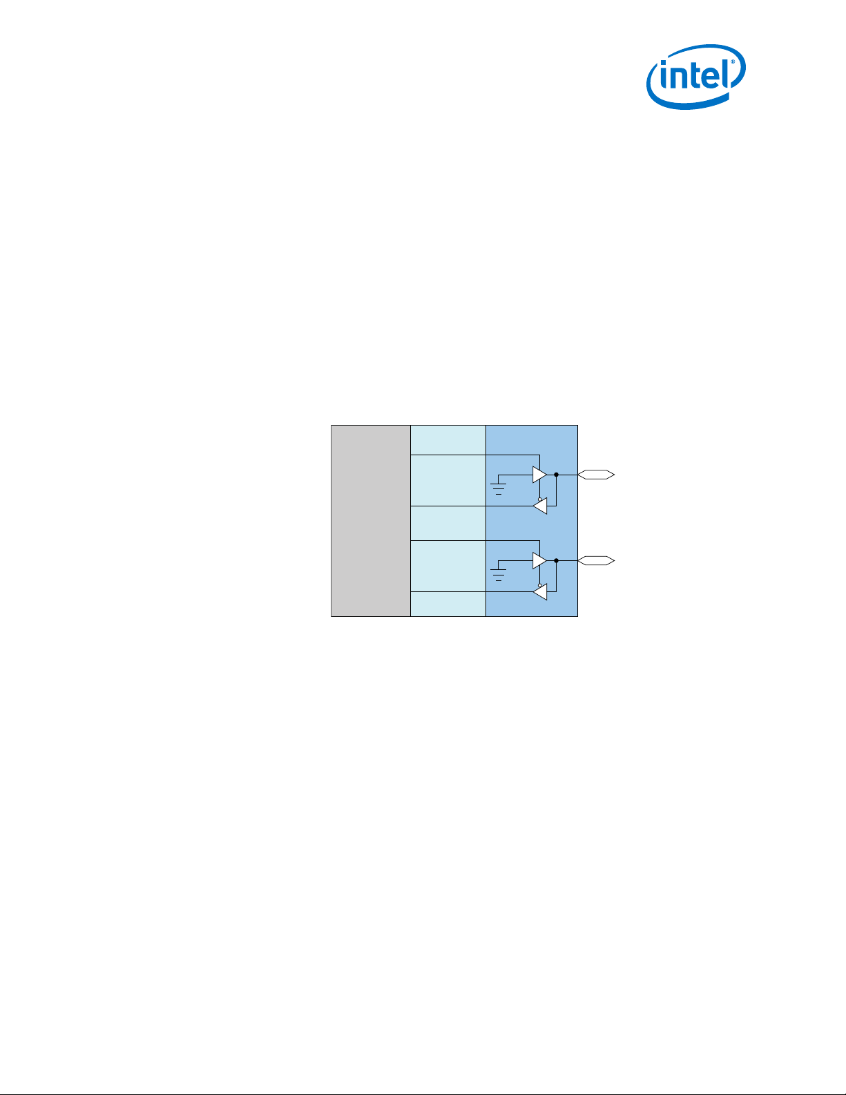
i2c*_out_data
i2c*_in_data
i2c*_out_clk
i2c*_in_clk
HPS FPGA Fabric FPGA I/O
4. Board Design Guidelines for SoC FPGAs
AN-796 | 2018.06.18
4.5.7. I2C Interface Design Guidelines
GUIDELINE: Instantiate the open-drain buffer when routing I2C signals
through the FPGA fabric.
When routing I2C signals through the FPGA, note that the I2C pins from the HPS to the
FPGA fabric (i2c*_out_data, i2c*_out_clk) are not open-drain and are logic level
inverted. Thus, when you want to drive a logic level zero onto the I2C bus, these pins
are high. This implementation is useful as they can be used to tie to an output enable
of a tri-state buffer directly. You must use the altiobuf to implement the open-drain
buffer.
GUIDELINE: Ensure that the pull-ups are added to the external SDA and SCL
signals in the board design.
Because the I2C signals are open drain, pull-ups are required to make sure that the
bus is pulled high when no device on the bus is pulling it low.
Figure 5. I2C Wiring to FPGA pins
4.5.8. SPI Interface Design Guidelines
GUIDELINE: Consider routing SPI slave signals to FPGA fabric
Due to an erratum in the Cyclone V/Arria V SoC device, the SPI output enable is not
connected to the SPI HPS pins. As a result, the HPS SPIS_TXD pin cannot be tristated by setting the slv_oe bit (bit 10) in the ctrlr0 register to 1.
Routing the SPI Slave signals to FPGA exposes the output enable signal and allows you
to connect it to an FPGA tri-state pin.
GUIDELINE: If your SPI peripheral requires the SPI master slave select to
stay low during the entire transaction period, consider using GPIO as slave
select, or configure the SPI master to assert slave select during the
transaction.
By default, the SPI master is configured with ctrlr0.scph = 0 and ctrlr0.scpol
= 0, which makes the Cyclone V or Arria V HPS SPI master deassert the slave select
signal between each data word. Set ctrlr0.scph to 1 and ctrlr0.scpol to 1, to
make the SPI master assert slave select for the entire duration of the transfer.
AN 796: Cyclone V and Arria V SoC Device Design Guidelines
47
Page 48

4. Board Design Guidelines for SoC FPGAs
AN-796 | 2018.06.18
Alternatively, consider routing the SPI master peripheral to FPGA, and using GPIO to
control the slave select signal.
Note: If you use this method, refer to the following Knowledge Base articles:
• Why does connecting HPS peripheral clocks to external pins via FPGA logic cause
Quartus fitter errors?
• Why does the HPS SPI Master fail when slave select is mapped to GPIO?
Related Information
• ctrlr0
For details about the ctrlr0.scph and ctrlr0.scpol bits in the Cyclone V
HPS, refer to "ctrlr0" in the "SPI Master" chapter of the Cyclone V Hard
Processor System Technical Reference Manual.
• ctrlr0
For details about the ctrlr0.scph and ctrlr0.scpol bits in the Arria V
HPS, refer to "ctrlr0" in the "SPI Master" chapter of the Arria V Hard Processor
System Technical Reference Manual.
AN 796: Cyclone V and Arria V SoC Device Design Guidelines
48
Page 49

Start
Select
Operating
System
Partner (RT)OSLinux
End
Select SoC Device
Start with Golden Hardware
Reference Design (GHRD)
Start with HWLibs Examples
from SoC EDS Getting Started
Guides
Start with GSRD for Linux from
Rocketboards.org
Start with Partner-Provided
(RT)OS BSP and Examples
Write/Modify Bare-Metal
Applications/Drivers
Write/Modify Linux
Applications/Drivers
Write/Modify (RT)OS
Applications/Drivers
Hardware
Software
Bare Metal
AN-796 | 2018.06.18
5. Embedded Software Design Guidelines for SoC FPGAs
5.1. Embedded Software for HPS: Design Guidelines
5.1.1. Assembling the Components of Your Software Development Platform
To successfully build your software development platform, Intel recommends that you
start with a baseline project, which is a known good configuration of an HPS system.
Then modify the baseline project to suit your end application.
The following diagram presents the recommended procedure to determine the
software development platform components.
Figure 6. Assembling Software Development Platform
Intel Corporation. All rights reserved. Intel, the Intel logo, Altera, Arria, Cyclone, Enpirion, MAX, Nios, Quartus
and Stratix words and logos are trademarks of Intel Corporation or its subsidiaries in the U.S. and/or other
countries. Intel warrants performance of its FPGA and semiconductor products to current specifications in
accordance with Intel's standard warranty, but reserves the right to make changes to any products and services
at any time without notice. Intel assumes no responsibility or liability arising out of the application or use of any
information, product, or service described herein except as expressly agreed to in writing by Intel. Intel
customers are advised to obtain the latest version of device specifications before relying on any published
information and before placing orders for products or services.
*Other names and brands may be claimed as the property of others.
ISO
9001:2015
Registered
Page 50

In summary, the process consists of following steps:
1. Select the desired device
2. Use the GHRD as a hardware project starting point
3. Select the operating slystem: bare metal, Linux or partner real-time operating
system
4. Write and/or update end application and/or drivers
5.1.1.1. Golden Hardware Reference Design
The Golden Hardware Reference Design is an Intel Quartus Prime project that contains
a full HPS design for the Cyclone V SoC / Arria V SoC Development Kit. The GHRD has
connections to a boot source, SDRAM memory and other peripherals on the
development board.
For every new released version of SoC EDS, the GHRD is included in the SoC EDS
tools. The GHRD is regression tested with every major release of the Intel Quartus
Prime Design Software and includes the latest bug fixes for known hardware issues.
The GHRD serves as a known good configuration of an SoC FPGA hardware system.
5. Embedded Software Design Guidelines for SoC FPGAs
AN-796 | 2018.06.18
AN 796: Cyclone V and Arria V SoC Device Design Guidelines
50
Page 51

Trace Memory Controller
USB OTG
Gbps Ethernet
SD/MMC
QSPI
GPIO
I2C
UART
CAN
Timers
FPGA Manager
DMA
ROM
RAM 64 KB
L2 DDR
HPS-to-FPGA
M
Lightweight
HSP-to-FPGA
M
FPGA-to-HPS
S
System ID S
PIO LED S
PIO Button S
PIO DIP Switch S
JTAG UART S
On-Chip RAM S
Non-Secure
JTAG Master
(FPGA Only)
M
Interrupt CapturerS
Secure
JTAG Master
(HPS Only)
M
Hard Processor
System
FPGA Fabric
I-Cache D-Cache I-Cache D-Cache
CPU0 CPU1
ARM Coretex-A9 MPCore
5. Embedded Software Design Guidelines for SoC FPGAs
AN-796 | 2018.06.18
Figure 7. Cyclone V / Arria V SoC Golden Hardware Reference Design Overview
The GHRD has a minimal set of peripherals in the FPGA fabric, because the HPS
provides a substantial selection of peripherals. HPS-to-FPGA and FPGA-to-HPS
interfaces are configured to a 64-bit data width.
GUIDELINE: Intel recommends that you use the latest GHRD as a baseline for
new SoC FPGA hardware projects. You may then modify the design to suit
your application ends.
The GHRD can be obtained from:
AN 796: Cyclone V and Arria V SoC Device Design Guidelines
51
Page 52

5. Embedded Software Design Guidelines for SoC FPGAs
• The GSRD for Linux page for the latest version, which is the best known
configuration
•
<SoC EDS installation directory>\examples\hardware
\cv_soc_devkit_ghrd - for the version supported by the corresponding SoC
EDS version, used as a basis for the provided HWLibs design examples.
5.1.2. Selecting an Operating System for Your Application
5.1.2.1. Linux or RTOS
There are a number of operating systems that support the Cyclone V SoC and Arria V
SoC, including Linux and several real-time operating systems (RTOSs). For more
information on Intel’s SoC Partner OS ecosystem, visit the Ecosystem tab of the Intel
FPGAs page.
Partner OS providers offer board support packages and commercial support for the
SoC FPGA devices. The Linux community also offers board support packages and
community support for the SoC FPGA device.
There are many factors that go into the selection of an operation system for SoC
FPGAs including the features of the operating system, licensing terms, collaborative
software projects and framework based on the OS, available device drivers and
reference software, in-house legacy code and familiarity with the OS, real-time
requirements of your system, functional safety and other certifications required for
your application.
AN-796 | 2018.06.18
To select an appropriate OS for your application, it is recommended that you
familiarize yourself with the features and support services offered by the commercial
and open source operating systems available for the SoC FPGA. Intel’s OS partners,
industry websites are a good source of information you can use to help make your
selection.
There are a number of misconceptions when it comes to real-time performance of
operating systems versus bare metal applications. For a Cortex A-class of processor
there are a number of features that real-time operating systems provide that make
efficient use of the processor’s resources in addition to the facilities provided to
manage the run-time application. You may find that these efficiencies result in
sufficient real-time performance for your application, enabling you to inherit a large
body of available device drivers, middleware packages, software applications and
support services. It is important to take this account when selecting an operating
system.
5.1.2.2. Bare Metal
The HPS can be used in a bare-metal configuration (without an OS) and Intel offers
the HWLibs (Hardware Libraries) that consist of both high-level APIs, and low-level
macros for most of the HPS peripherals.
However, to use a bare metal application for the HPS, you must be familiar with
developing run time capabilities to ensure that your bare metal application makes
efficient use of resources available in your MPU subsystem.
For example:
AN 796: Cyclone V and Arria V SoC Device Design Guidelines
52
Page 53

5. Embedded Software Design Guidelines for SoC FPGAs
AN-796 | 2018.06.18
• A typical bare-metal application uses only a single core, you must develop run
time capabilities to manage process between both cores and the cache subsystem
if you want to fully utilize the MPU subsystem.
• As your application increases in complexity you may need to build capabilities to
manage and schedule processes, handle inter-process communication and
synchronize between events within your application.
Even a small, lightweight RTOS offers simple scheduling, inter-process communication
and interrupt handling capabilities that make efficient use of the resources in the MPU
subsystem.
5.1.2.3. Using Symmetrical vs. Asymmetrical Multiprocessing (SMP vs. AMP) Modes
The Dual Core ARM Cortex-A9 MPCore* in the Cyclone V / Arria V HPS can support
both Symmetrical Multi-processing (SMP) and Asymmetrical Multi-processing (AMP)
configuration modes.
In SMP mode, a single OS instance controls both cores. The SMP configuration is
supported by a wide variety of operating system manufacturers and is the most
common and straightforward configuration mode for multiprocessing.
Commercially developed operating systems offer features that take full advantage of
the CPU cores resources and use them in an efficient manner resulting in optimum
performance and ease of use. For instance, SMP enabled operating systems offer the
option of setting processor affinity. This means that each task/thread can be assigned
to run on a specific core. This feature allows the software developer to better control
the workload distribution for each Cortex-A9 core and making the system more
responsive as an alternative to AMP.
GUIDELINE: Familiarize yourself with the performance and optimizations
available in commercial operating systems to see if an SMP-enabled OS or
RTOS meets your performance and real-time requirements.
In the AMP (Asymmetrical Multi-Processing) configuration, two different operating
systems or two instances of a single operating system run on the two cores. The two
operating systems have no inherent knowledge of how they share CPU resources. To
ensure efficient use of MPU subsystem resources in this environment, you must deal
with several complex issues when designing your system.
Caution: Use AMP only if you are familiar with the techniques to manage and schedule
processes, handle inter-process communication, synchronize between events, manage
secure processes between the two instances of the operating systems.
Note: OS providers do not generally offer support for using their OS in an AMP mode, so a
special support agreement is typically needed in this case.
5.1.3. Assembling your Software Development Platform for Linux
This section presents design guidelines to be used when you have selected Linux as
the OS for your end application.
AN 796: Cyclone V and Arria V SoC Device Design Guidelines
53
Page 54

5. Embedded Software Design Guidelines for SoC FPGAs
5.1.3.1. Golden System Reference Design (GSRD) for Linux
The Golden System Reference Design (GSRD) for Linux is provided, which consists of
the following:
• GHRD (Golden Hardware Reference Design) - A Quartus Prime project
• Reference U-Boot based Bootloader
• Reference Linux BSP
• Sample Linux Applications
Figure 8. GSRD for Linux - Overview
AN-796 | 2018.06.18
The GSRD for Linux is a well-tested known good design showcasing a system using
both HPS and FPGA resources, intended to be used as a baseline project.
GUIDELINE: To successfully build your software development platform, it is
recommended that you use the GSRD as a baseline project, then modify it to
suit your application needs.
The GSRDs target the Intel SoC Development Boards and are provided both in source
and pre-compiled form. They can be obtained from GSRD User Manuals.
GUIDELINE: It is recommended that all new projects use the latest version of
GSRD as a baseline.
5.1.3.2. GSRD for Linux Development Flow
The figure below presents a high-level view of the development flow for projects based
on the GSRD. Refer to the GSRD User Manuals link given below for more details.
AN 796: Cyclone V and Arria V SoC Device Design Guidelines
54
Page 55

5. Embedded Software Design Guidelines for SoC FPGAs
AN-796 | 2018.06.18
Figure 9. GSRD for Linux - Development Flow
Related Information
GSRD User Manuals
5.1.3.3. GSRD for Linux Build Flow
The figure below presents a detailed build flow for the GSRD. Refer to the GSRD User
Manuals link given below for more details.
AN 796: Cyclone V and Arria V SoC Device Design Guidelines
55
Page 56

Figure 10. GSRD for Linux - Build Flow
5. Embedded Software Design Guidelines for SoC FPGAs
AN-796 | 2018.06.18
The above build flow is the one used for the GSRD for Linux but it can be tweaked to
match the individual needs of each project. For example:
• Linux kernel could be built separately without using Yocto Bitbake.
• Linux filesystem could be built separately without using Yocto Project.
• Linux Device Tree could be managed without using the Device Tree Generator. For
example, it can be manually edited.
Related Information
GSRD User Manuals
5.1.3.4. Linux Device Tree Design Considerations
The Linux Device Tree is a data structure that describes the underlying hardware to
the Linux operating system kernel. By passing this data structure the OS kernel, a
single OS binary may be able to support many variations of hardware. This flexibility is
particularly important when the hardware includes an FPGA.
The recommended procedure for managing the Linux Device Tree is:
AN 796: Cyclone V and Arria V SoC Device Design Guidelines
56
Page 57

5. Embedded Software Design Guidelines for SoC FPGAs
AN-796 | 2018.06.18
1. Start with the SoC FPGA reference Device Trees provided in the Linux kernel
source code that targets the Intel SoC development kits. They cover the HPS
portion of the device but do not cover the FPGA portion which changes on a perproject basis. SD/MMC and QSPI versions are provided with the kernel source
code.
2. Edit the Device Tree as necessary to accommodate any board changes as
compared to the Intel SoC development kit.
3. Edit the Device Tree as necessary to accommodate the Linux drivers targeting
FPGA Soft IP.
Note: The GSRD for Linux uses a different flow that the one recommended above relying on
a custom tool called “Linux Device Tree Generator” that is provided as part of SoC
EDS.
Figure 11. Device Tree Generation Flow for GSRD for Linux
Refer to the DeviceTree Generator User Guide link given below for more details
about the Linux Device Tree Generator.
Related Information
DeviceTree Generator User Guide
5.1.4. Assembling a Software Development Platform for a Bare-Metal Application
Intel hardware libraries (HWLibs) are low level bare metal software libraries provided
with SoC EDS and various components of the HPS. The HWLibs are also typically used
by Intel’s OS partners to build board support packages for operating systems.
The HWLibs have two components:
• SoC Abstraction Layer (SoCAL): Symbolic register abstraction later that enables
direct access and control of HPS device registers within the address space.
• Hardware Manager (HWMgr): APIs that provide more complex functionality and
drivers for higher level use case scenarios.
AN 796: Cyclone V and Arria V SoC Device Design Guidelines
57
Page 58

Figure 12. HWLibs Overview
Bare Metal Application
HWMgr
SoCAL
Hardware
Note that not all hardware is covered by SoCAL and HWMgr, therefore writing custom
code might be necessary depending on the application. Software applications that use
HWLibs should have run time provisions to manage the resources of the MPU
subsystem, the cache and memory. These provisions are typically what the operating
systems provide.
5. Embedded Software Design Guidelines for SoC FPGAs
AN-796 | 2018.06.18
GUIDELINE: It is recommended using HWLibs only if you are familiar with
developing a run time provision to manage your application.
GUIDELINE: Use the HWLibs Project Generator to create your customized
HWLibs project.
Intel recommends that you create your custom HWLibs project using the HWLibs
Project Generator tool, available at Creating a Bare-metal HwLibs Project
Automatically.
Related Information
• Intel® SoC FPGA Embedded Development Suite User Guide
• Creating a Bare-metal HwLibs Project Automatically
• Getting Started with HwLibs Baremetal Development
• Design Examples
Additional HWLibs examples
5.1.5. Assembling your Software Development Platform for a Partner OS or RTOS
Partner OS providers offer board support packages and commercial support for the
SoC FPGA devices. Typically, partner support includes example getting-started projects
and associated documentation.
Note: Please refer to the partner documentation and support services for information on how
to assemble the software development platform when targeting a partner OS or RTOS.
5.1.6. Choosing Boot Loader Software
The Cyclone V / Arria V SoC boot flow includes the following stages:
AN 796: Cyclone V and Arria V SoC Device Design Guidelines
58
Page 59

5. Embedded Software Design Guidelines for SoC FPGAs
AN-796 | 2018.06.18
1. Boot ROM
2. Preloader
3. Bootloader
4. Real-time operating system or bare-metal application
Figure 13. Cyclone V / Arria V SoC Boot Flow
The BootROM and Preloader stages are needed for all Cyclone V SoC / Arria V SoC
applications. U-boot and Linux are used by the GSRD, but a custom application may
implement a different flow, such as using the Preloader to load a bare-metal
application directly.
Typically, the main responsibilities of the Preloader are:
• Perform additional HPS initialization
• Bring up SDRAM
• Load the next boot stage from Flash to SDRAM and jump to it
Currently, two different Preloader options are available:
• SPL - part of U-Boot. Provided with SoC EDS under GPL (Open Source) License
• MPL - provided with SoC EDS as an example using the HWLibs (bare-metal
libraries). Uses BSD license.
Note: The Preloader requires a special header to be placed at the beginning of the next
stage boot image. Also, the header contains a CRC value used to validate the image.
The header can be attached to an image by using the mkimage utility that is included
with SoC EDS.
The Bootloader has typical responsibilities that are similar with the Preloader, except it
does not need to bring up SDRAM. Because the Bootloader is already residing in
SDRAM, it is not limited by the size of the OCRAM. Therefore, it can provide a lot of
features, such as network stack support.
A typical HPS system had numbers of registers that need to be set for a given
configuration of the MPU subsystem, the network-on-chip interconnect component, the
SDRAM memory, flash boot source and peripheral interfaces. The settings used for
boot or initialization purposes are encapsulated in the following places:
• RBF File(s) - containing register settings for SDRAM also dedicated I/O and FPGA
pin configuration.
• U-Boot source code - for rest of the settings
AN 796: Cyclone V and Arria V SoC Device Design Guidelines
59
Page 60
5. Embedded Software Design Guidelines for SoC FPGAs
AN-796 | 2018.06.18
Figure 14. Preloader Build Flow
Note: It is highly recommended that Preloader is generated with bsp-editor. It is also
recommended, although not required, to build U-Boot from the same source code.
5.1.7. Selecting Software Tools for Development, Debug and Trace
Note: When using a specific Partner OS or RTOS, consult the OS vendor and the OS
documentation for any specific tools that are required. Some OS vendors also provide
a full set of tools that are recommended to be used with that OS.
Note: Familiarize yourself with the available tools for development, compilation and debug. A
list of supported tools is available at the Ecosystem tab of the Intel FPGAs page.
5.1.7.1. Select Software Build Tools
GUIDELINE: Decide which software development tools to use, and select the
tool versions.
Software development tools include compilers, assemblers, linkers, and archivers. The
Arm Development Studio 5* (DS-5*) Intel SoC FPGA Edition includes the following
software build tools:
• ARMCC Bare-metal Compiler
• Mentor Graphics CodeSourcery Lite GCC-based bare-metal Compiler
• Linux Linaro Compiler
There are also other development tools offerings from third party providers.
5.1.7.2. Select Software Debug Tools
GUIDELINE: Select software debug tools.
Arm DS-5 Intel SoC FPGA Edition includes a fully featured Eclipse-based debugging
environment. There are also other debugging tools offerings from third party providers
such as Lauterbach T32.
The debug tools require a JTAG connection to the SoC FPGA device. The connection
could be achieved in a couple of ways:
• An embedded USB-Blaster II chip could be available on-board such as on the
Cyclone V SoC / Arria V SoC Development Kit.
• External JTAG hardware may be required when using the Lauterbach T32 tools.
AN 796: Cyclone V and Arria V SoC Device Design Guidelines
60
Page 61

5. Embedded Software Design Guidelines for SoC FPGAs
AN-796 | 2018.06.18
5.1.7.3. Select Software Trace Tools
Tracing can be very helpful for profiling performance bottlenecks, debugging crash
scenarios and debugging complex cases. Tracing can be performed in two ways:
• Non-real-time: by storing trace data in system memory (for example SDRAM) or
the embedded trace buffer, then stopping the system, downloading the trace
information and analyzing it.
• Real-time: by using an external adapter trace data from the trace port. The
target board needs to support this scenario.
Typically, the debug tools also offer tracing of the embedded software program
execution, but external hardware may be required. For example, the DS-5 provided
with the SoC EDS supports both non-real-time and real-time tracing. When used for
real-time tracing, an additional external trace unit called “DSTREAM” is required.
Lauterbach T32 is a similar example, in that it needs additional external hardware for
real-time tracing.
5.2. Flash Device Driver Design Considerations
The SoC FPGAs support the following types of flash devices: QSPI, NAND, SD/MMC/
eMMC.
Note: Please refer to Supported Flash Devices for Cyclone V and Arria V SoC for a list of
supported flash devices. Use an “Intel Tested and Supported” device, to minimize
development effort and risk of incompatibility. The next best option is to select a
“Known to Work” device. This means that the device is compatible with BootROM and
was proven to work with at least one Bootloader - but it may not be the Bootloader
you need. It may also not have HWLibs, OS Support or HPS Flash Programmer
Support.
5.3. HPS ECC Design Considerations
ECC is implemented throughout the entire HPS subsystem on all RAMs, including the
external HPS EMIF, L2 cache data RAMs and all peripheral RAMs. The controller ECC
employs standard Hamming logic to detect and correct single-bit errors and detect
double-bit errors. Parity protection is provided for the Cortex-A9 MPCore L1 cache
memories and L2 tag RAM. ECC can be selectively enabled on the HPS EMIF and
internal HPS RAMs. Diagnostic test modes and error injection capability are available
under software control. ECC is disabled by default upon power-up or cold reset.
The generated boot code configures, initializes and enables ECC according to user
options selected during BSP generation. Custom firmware and bare metal application
code access to the ECC features is facilitated with the Intel-provided HWLibs library,
which provides a simple API for programming HPS software features.
For more information, refer to the "Boot Tools User Guide" and "Hardware Library"
chapters of the Intel SoC FPGA Embedded Development Suite User Guide.
Related Information
Intel® SoC FPGA Embedded Development Suite User Guide
AN 796: Cyclone V and Arria V SoC Device Design Guidelines
61
Page 62

5. Embedded Software Design Guidelines for SoC FPGAs
AN-796 | 2018.06.18
5.3.1. General ECC Design Considerations
Each RAM in the HPS subsystem has its own ECC controller with a unique set of
features and requirements. However, there are general system integration design
issues that you should consider.
5.3.2. System-Level ECC Control, Status and Interrupt Management
The System Manager contains a set of ECC-related registers for system-level control
and status for all the ECC controllers in the HPS subsystem. ECC-related interrupts are
also managed through this set of registers.
Related Information
• System Manager - Cyclone V Hard Processor System Technical Reference Manual
• System Manager - Arria V Hard Processor System Technical Reference Manual
5.3.3. ECC for L2 Cache Data Memory
The L2 cache memory is ECC protected, while the tag RAMs are parity protected. L2
cache ECC is enabled through a control register in the System Manager.
For details about the L2 cache ECC controller, refer to the following sections in the
"Cortex-A9 Microprocessor Unit Subsystem" chapter of the appropriate Hard Processor
System Technical Reference Manual:
• “Single Event Upset Protection”
• “L2 Cache Controller Address Map for Cyclone V” or "L2 Cache Controller Address
Map for Arria V"
GUIDELINE: The L1 and L2 cache must be configured as write-back and
write-allocate for any cacheable memory region with ECC enabled.
For BSPs supported by the Intel SoC FPGA EDS, you can configure your BSP for ECC
support with the bsp-editor utility.
For bare metal firmware, refer to "L2 Cache Controller Address Map" in the "Cortex-A9
Microprocessor Unit Subsystem" chapter of the appropriate Hard Processor System
Technical Reference Manual.
GUIDELINE: Cache-coherent accesses through the L3 interconnect using the
ACP must perform 64-bit wide, 64-bit aligned write accesses when ECC is
enabled in the L2 Cache Controller
Enabling ECC does not affect the performance of the L2 cache, but accesses using the
ACP must be 64-bit wide, 64-bit aligned in memory. This includes FPGA masters
accessing the ACP over the FPGA-to-HPS Bridge. For a list of possible combinations of
bridge width and FPGA master width, alignment and burst size and length, refer to
"FPGA-to-HPS Access to ACP" in the "HPS-FPGA Bridges" chapter of the appropriate
Hard Processor System Technical Reference Manual.
Related Information
• Cyclone V Hard Processor System Technical Reference Manual
• Arria V Hard Processor System Technical Reference Manual
AN 796: Cyclone V and Arria V SoC Device Design Guidelines
62
Page 63

5. Embedded Software Design Guidelines for SoC FPGAs
AN-796 | 2018.06.18
5.3.4. ECC for Flash Memory
All peripheral RAMs in the HPS subsystem are ECC protected. The NAND flash
controller ECC hardware is not used when a read-modify-write operation is performed
from the flash device’s page buffer. Software must update the ECC during such readmodify-write operations. For a read-modify-write operation to work with hardware
ECC, the entire page must be read into system memory, modified, then written back
to flash without relying on the flash device’s read-modify-write feature.
The NAND flash controller cannot do ECC validation during a copy-back command. The
flash controller copies the ECC data but does not validate it during the copy operation.
5.4. HPS SDRAM Considerations
5.4.1. Using the Preloader To Debug the HPS SDRAM
To debug the HPS EMIF, you can change the settings in the preloader to enable
runtime calibration report, debug level information and check the status of HPS
SDRAM PLL.
Note: Refer to "Building the Second Stage Bootloader" in the Intel SoC FPGA Embedded
Development Suite User Guide for step-by-step instructions for compiling the
preloader.
Related Information
Intel® SoC FPGA Embedded Development Suite User Guide
5.4.1.1. Enable Runtime Calibration Report
To enable the runtime calibration report, use your preferred editor to open the
<project_folder>\software\spl_bsp\uboot-socfpga\board\altera
\socfpga\sdram\sequencer_defines.h file and configure the
RUNTIME_CAL_REPORT value to 1.
AN 796: Cyclone V and Arria V SoC Device Design Guidelines
63
Page 64

5. Embedded Software Design Guidelines for SoC FPGAs
AN-796 | 2018.06.18
5.4.1.2. Change DLEVEL To Get More Debug Information
5.4.1.3. Enable Example Driver for HPS SDRAM
• Enable with Hardware Diagnostic Option in bsp-editor. Note: Example driver is
only available in Intel Quartus Prime version 14.0 and later.
— PRBS31 Data pattern
— Write to random address => Read from random address
— Can select different coverage by changing parameter in spl.c
AN 796: Cyclone V and Arria V SoC Device Design Guidelines
64
Page 65

5. Embedded Software Design Guidelines for SoC FPGAs
AN-796 | 2018.06.18
5.4.1.4. Change Data Pattern in Example Driver
1.
Path for sdram_test.c: <project_folder>\software\spl_bsp\uboot-
socfpga\arch\arm\cpu\armv7\socfpga\sdram_test.c
2.
Change the test_rand_address function
AN 796: Cyclone V and Arria V SoC Device Design Guidelines
65
Page 66

5. Embedded Software Design Guidelines for SoC FPGAs
AN-796 | 2018.06.18
5.4.1.5. Example Code to Write and Read from All Addresses
5.4.1.6. Read/Write to HPS Register in Preloader
Use the following function:
1.
writel to write to HPS register
AN 796: Cyclone V and Arria V SoC Device Design Guidelines
66
Page 67

5. Embedded Software Design Guidelines for SoC FPGAs
AN-796 | 2018.06.18
•
writel(value, address);
2.
readl to read from HPS register
•
readl(address);
For example:
5.4.1.7. Check HPS PLL Lock Status in Preloader
•
Read HPS PLL Status Register in clock_manager.c and print out in spl.c
—
Define global variable in clock_manager.c and “extern variable” in spl.c
—
Unable to printout value in clock_manager.c as the UART has not been
initialized yet
5.4.2. Access HPS SDRAM via the FPGA-to-SDRAM Interface
The HPS bridges can be enabled from the Preloader (SPL/MPL) or U-Boot and in some
cases from Linux.
Note: Preloaders (SPL) and U-Boot generated from SoC EDS 13.1 and later contain extra
functionality and built in functions to safely enable the HPS bridges.
To enable the HPS FPGA-to-SDRAM bridge from the Preloader or U-Boot, follow the
appropriate steps.
AN 796: Cyclone V and Arria V SoC Device Design Guidelines
67
Page 68

5. Embedded Software Design Guidelines for SoC FPGAs
AN-796 | 2018.06.18
Enabling HPS-to-FPGA Bridges from the Preloader
The Preloader checks the status of the FPGA and automatically enables bridges
configured in Platform Designer (Standard) and the BSP if the FPGA is configured. The
Preloader supports programming the FPGA before running automatic bridge enable
tests and code.
For more information, refer to GSRD v13.1 - Programming FPGA from HPS.
Enabling HPS-to-FPGA Bridges from U-Boot
The bridge_enable_handoff command can be run from the U-boot command
prompt to enable bridges. This command puts the HPS and SDRAM into a safe state
before enabling all bridges after appropriate checks.
For more information, refer to the KDB solution: How can I enable the FPGA2SDRAM
bridge on Cyclone V SoC and Arria V SoC Devices?
AN 796: Cyclone V and Arria V SoC Device Design Guidelines
68
Page 69

AN-796 | 2018.06.18
A. Support and Documentation
A.1. Support
Technical support for operating system board support packages (BSPs) that are ported
to the Intel SoC development kit is provided by the operating system provider.
Support for the Intel SoC FPGA Embedded Development Suite (EDS) and the design
tools for FPGA development are provided by Intel. The EDS includes the ARM
Development Studio 5 (DS-5) Intel Edition Toolkit.
Support of the Intel SoC development kit is provided by Intel.
Technical Support for other boards is provided by the respective board provider or
distributor.
Item Supported Through
Commercial OS/Tools OS/Tools Vendor
Hardware libs (bare metal) Intel
Intel SoC FPGA EDS Intel
ARM DS-5 Intel Edition Intel
FPGA design tools Intel
Open Source / Linux RocketBoards.org
UBoot RocketBoards.org
For additional information, please refer to these links given below.
Related Information
• Ecosystem tab of the Intel FPGAs page
• Support
Support for Intel FPGA products
• End Market Related Designs
Reference designs and design examples for Intel FPGA products
• Intel FPGA Design Solutions Network
• Embedded Support Center
• Design Examples for Intel FPGA products
• Development Kits, Daughter Cards & Programming Hardware Support
• Intel Wiki
Intel Corporation. All rights reserved. Intel, the Intel logo, Altera, Arria, Cyclone, Enpirion, MAX, Nios, Quartus
and Stratix words and logos are trademarks of Intel Corporation or its subsidiaries in the U.S. and/or other
countries. Intel warrants performance of its FPGA and semiconductor products to current specifications in
accordance with Intel's standard warranty, but reserves the right to make changes to any products and services
at any time without notice. Intel assumes no responsibility or liability arising out of the application or use of any
information, product, or service described herein except as expressly agreed to in writing by Intel. Intel
customers are advised to obtain the latest version of device specifications before relying on any published
information and before placing orders for products or services.
*Other names and brands may be claimed as the property of others.
ISO
9001:2015
Registered
Page 70

A.2. Software Documentation
Driven by the feature-updating nature of today’s open source embedded software,
most of our software documentation is also hosted on community web.
For more information, please refer to the links given below.
Related Information
• RocketBoards.org Documentation Portal
• Altera Opensource
RocketBoards.org repository of Linux-related source code
• RocketBoards.org Boards
• RocketBoards.org Projects
• Intel SoC FPGA Embedded Development Suite User Guide
• Download SoC EDS
Getting Started tab of the Intel SoC FPGA Embedded Development Suite
page
A. Support and Documentation
AN-796 | 2018.06.18
AN 796: Cyclone V and Arria V SoC Device Design Guidelines
70
Page 71

AN-796 | 2018.06.18
B. Additional Information
B.1. Cyclone V and Arria V SoC Device Guidelines Revision History
Document Version Description
2018.06.18 Updated the "Early Power Estimation" section to include information for CVSoC
2017.12.22 • Update product names
L.
• "Background: Comparison between SoC FPGA and SoC FPGA HPS
Subsystem" chapter:
— Remove overview and block diagram of L3 interconnect
— Remove SDRAM controller block diagram
— Clarify description of FPGA-to-SDRAM access
— Remove detailed descriptions of HPS-FPGA system topologies
— Guidelines added:
• Use the lightweight HPS-to-FPGA bridge to connect IP that needs to be
controlled by the HPS.
• Do not use the lightweight HPS-to-FPGA bridge for FPGA memory.
Instead use the HPS-to-FPGA bridge for memory.
• Use the HPS-to-FPGA bridge to connect memory hosted by the FPGA
to the HPS..
• If memory connected to the HPS-to-FPGA bridge is used for HPS boot,
ensure that its slave address is set to 0x0 in Platform Designer
(Standard).
• Use the FPGA-to-HPS bridge for cacheable accesses to the HPS from
masters in the FPGA.
• Use the FPGA-to-HPS bridge to access cache-coherent memory,
peripherals, or on-chip RAM in the HPS from masters in the FPGA.
• Use the FPGA-to-SDRAM ports for non-cacheable access to the HPS
SDRAM from masters in the FPGA.
• "Design Guidelines for HPS portion of SoC FPGAs" chapter:
— Recommend the Cyclone V HPS-FPGA Bridge Reference Design Example
instead of the Cyclone V Datamover Design Example
— GPIO not recommended for high-speed serial interfaces
— Guidelines added:
• Use the Golden System Reference Design (GSRD) as a starting point
for a loosely coupled system.
• Use the Cyclone V HPS-to-FPGA Bridge Design Example reference
design to determine your optimum burst length and data-width for
accesses between FPGA logic and HPS.
— Guidelines removed:
• Intel recommends that you use the Golden System Reference Design
(GSRD) as a starting point for a loosely coupled system.
• Intel recommends that you use the Cyclone V HPS-FPGA Bridge
Reference Design Example to optimize your hardware design and
software solutions to achieve high performance real time application
with HPS ARM processor.
continued...
Intel Corporation. All rights reserved. Intel, the Intel logo, Altera, Arria, Cyclone, Enpirion, MAX, Nios, Quartus
and Stratix words and logos are trademarks of Intel Corporation or its subsidiaries in the U.S. and/or other
countries. Intel warrants performance of its FPGA and semiconductor products to current specifications in
accordance with Intel's standard warranty, but reserves the right to make changes to any products and services
at any time without notice. Intel assumes no responsibility or liability arising out of the application or use of any
information, product, or service described herein except as expressly agreed to in writing by Intel. Intel
customers are advised to obtain the latest version of device specifications before relying on any published
information and before placing orders for products or services.
*Other names and brands may be claimed as the property of others.
ISO
9001:2015
Registered
Page 72

Document Version Description
• "Board Design Guidelines for SoC FPGAs" chapter:
— RGMII supported by HPS dedicated I/O
— Guidelines added:
• If your design uses QSPI flash with 4-byte addressing, design the
board to ensure that the QSPI flash is reset or power-cycled whenever
the HPS is reset.
• If your SPI peripheral requires the SPI master slave select to stay low
during the entire transaction period, consider using GPIO as slave
select, or configure the SPI master to assert slave select during the
transaction.
• Ensure that the SD/MMC card is reset whenever the HPS is reset.
• For bare-metal applications, avoid using a QSPI flash device larger
than 16 MB
• With a QSPI device larger than 16 MB, use QSPI extended 4-byte
addressing commands if supported by the device
• "Embedded Software Design Guidelines for SoC FPGAs" chapter:
— Reference DTB for NAND-based boot no longer supplied
— Clarify NAND flash interface type required for booting support
2017.02.20 Initial Release
B. Additional Information
AN-796 | 2018.06.18
AN 796: Cyclone V and Arria V SoC Device Design Guidelines
72
 Loading...