

Page 1

Intel® FPGA HDMI Design Example
User Guide for Intel® Arria 10
Devices
Updated for Intel® Quartus® Prime Design Suite: 17.1
Subscribe
Send Feedback
UG-20077 | 2017.11.06
Latest document on the web: PDF | HTML
Page 2

Contents
Contents
1 Intel® FPGA HDMI Design Example Quick Start Guide for Intel® Arria® 10 Devices......... 3
1.1 Directory Structure................................................................................................. 3
1.2 Hardware and Software Requirements.......................................................................7
1.3 Generating the Design.............................................................................................7
1.4 Simulating the Design............................................................................................. 8
1.5 Compiling and Testing the Design ............................................................................ 9
1.6 Design Limitation..................................................................................................10
1.7 Intel FPGA HDMI Design Example Parameters...........................................................10
2 Intel FPGA HDMI Design Example Detailed Description................................................. 11
2.1 HDMI RX-TX Retransmit Design Example..................................................................11
2.2 Design Components.............................................................................................. 13
2.3 Dynamic Range and Mastering (HDR) InfoFrame Insertion and Filtering....................... 20
2.4 Clocking Scheme.................................................................................................. 23
2.5 Interface Signals...................................................................................................26
2.6 Design RTL Parameters.......................................................................................... 36
2.7 Hardware Setup....................................................................................................37
2.8 Simulation Testbench............................................................................................ 38
A Intel FPGA HDMI Design Example User Guide for Intel Arria 10 Devices Archives......... 41
B Revision History for Intel FPGA HDMI Design Example User Guide for Intel Arria
10 Devices............................................................................................................... 42
Intel® FPGA HDMI Design Example User Guide for Intel® Arria 10 Devices
2
Page 3

Design
Example
Generation
Compilation
(Simulator)
Functional
Simulation
Compilation
(Quartus Prime)
Hardware
Testing
UG-20077 | 2017.11.06
1 Intel® FPGA HDMI Design Example Quick Start Guide for
Intel® Arria® 10 Devices
The Intel® FPGA HDMI IP core design example for Intel Arria® 10 devices features a
simulating testbench and a hardware design that supports compilation and hardware
testing.
When you generate a design example, the parameter editor automatically creates the
files necessary to simulate, compile, and test the design in hardware.
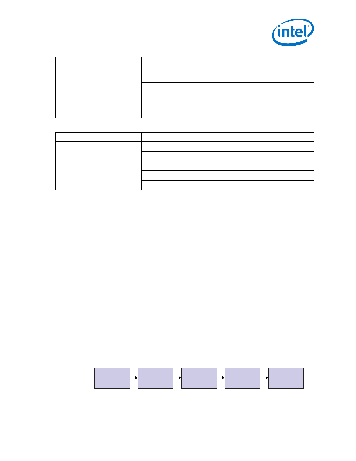
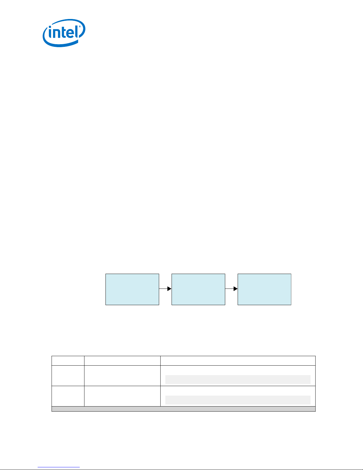
Figure 1. Development Steps
Related Links
Intel FPGA HDMI IP Core User Guide
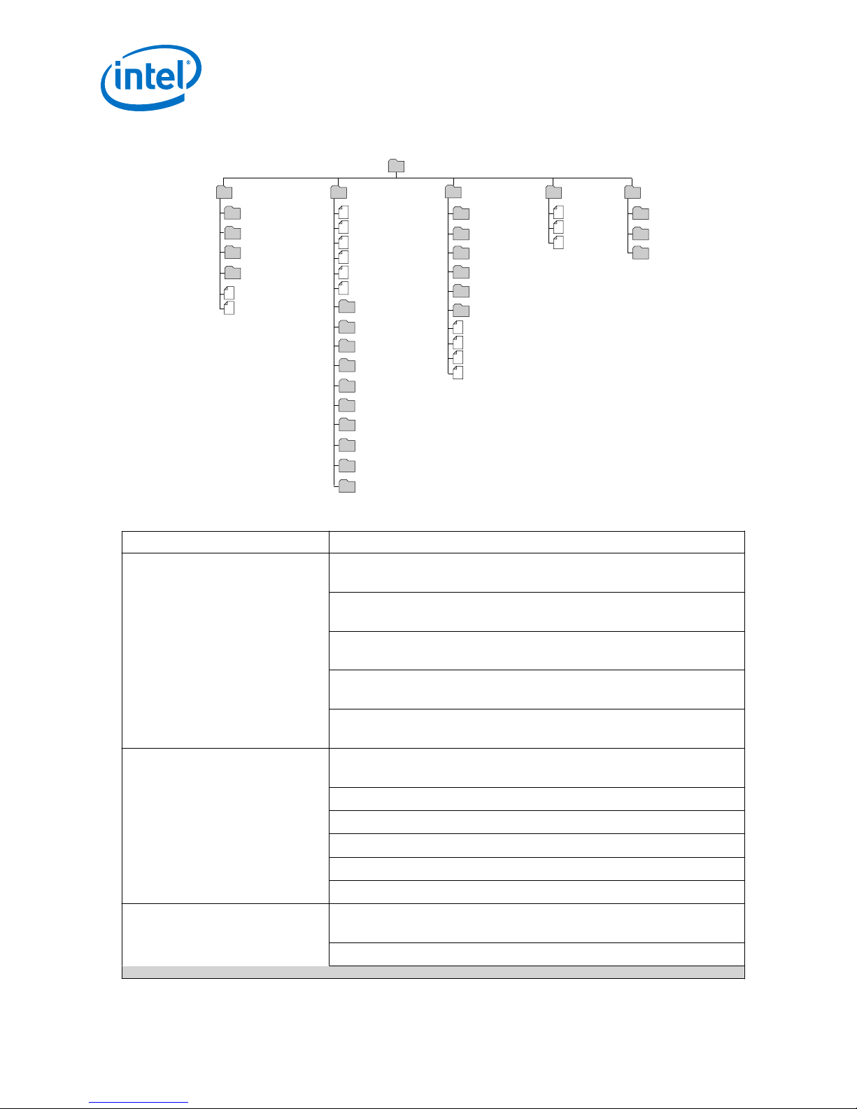
1.1 Directory Structure
The directories contain the generated files for the Intel FPGA HDMI design example.
Intel Corporation. All rights reserved. Intel, the Intel logo, Altera, Arria, Cyclone, Enpirion, MAX, Nios, Quartus
and Stratix words and logos are trademarks of Intel Corporation or its subsidiaries in the U.S. and/or other
countries. Intel warrants performance of its FPGA and semiconductor products to current specifications in
accordance with Intel's standard warranty, but reserves the right to make changes to any products and services
at any time without notice. Intel assumes no responsibility or liability arising out of the application or use of any
information, product, or service described herein except as expressly agreed to in writing by Intel. Intel
customers are advised to obtain the latest version of device specifications before relying on any published
information and before placing orders for products or services.
*Other names and brands may be claimed as the property of others.
ISO
9001:2008
Registered
Page 4
<Design Example>
* Standard = Intel Quartus Prime Standard Edition
Pro = Intel Quartus Prime Pro Edition
quartus
incremental_db (Standard)
db (Standard)/qdb (Pro)
output_files
tmp-clearbox (Pro)
a10_hdmi_demo.qpf
a10_hdmi_demo.qsf
rtl
nios.qsys
gxb
hdmi_rx
hdmi_tx
i2c_master
i2c_slave
reconfig_mgmt
sdc
hdr
common (Pro)
pll
rxtx_link.v
a10_hdmi2_demo.v
a10_reconfig_arbiter.sv
clock_control.qsys/clock_control.ip
clock_crosser.v
script
build_ip.tcl
build_sw.sh
runall.tcl
tx_control_bsp
tx_control
tx_control_src
software
simulation
aldec
cadence
mentor
synopsys
hdmi_rx
hdmi_tx
autotest_crc.v
bitec_hdmi_audio_gen.v
bitec_hdmi_tb.sv
tpg.v
1 Intel® FPGA HDMI Design Example Quick Start Guide for Intel® Arria® 10 Devices
Figure 2. Directory Structure for the Design Example
UG-20077 | 2017.11.06
Table 1. Generated RTL Files
Folders Files
gxb •
hdmi_rx •
Intel® FPGA HDMI Design Example User Guide for Intel® Arria 10 Devices
4
hdmi_tx •
/gxb_rx.qsys (Intel Quartus Prime Standard Edition)
•
/gxb_rx.ip (Intel Quartus Prime Pro Edition)
•
/gxb_rx_reset.qsys (Intel Quartus Prime Standard Edition)
•
/gxb_rx_reset.ip (Intel Quartus Prime Pro Edition)
•
/gxb_tx.qsys (Intel Quartus Prime Standard Edition)
•
/gxb_tx.ip (Intel Quartus Prime Pro Edition)
•
/gxb_tx_fpll.qsys (Intel Quartus Prime Standard Edition)
•
/gxb_tx_fpll.ip (Intel Quartus Prime Pro Edition)
•
/gxb_tx_reset.qsys (Intel Quartus Prime Standard Edition)
•
/gxb_tx_reset.ip (Intel Quartus Prime Pro Edition)
/hdmi_rx.qsys (Intel Quartus Prime Standard Edition)
•
/hdmi_rx.ip (Intel Quartus Prime Pro Edition)
/hdmi_rx_top.v
/mr_clock_sync.v
/mr_hdmi_rx_core_top.v
/mr_rx_oversample.v
/symbol_aligner.v
/hdmi_tx.qsys (Intel Quartus Prime Standard Edition)
•
/hdmi_tx.ip (Intel Quartus Prime Pro Edition)
/hdmi_tx_top.v
continued...
Page 5
1 Intel® FPGA HDMI Design Example Quick Start Guide for Intel® Arria® 10 Devices
UG-20077 | 2017.11.06
Folders Files
/mr_ce.v
/mr_hdmi_tx_core_top.v
/mr_tx_oversample.v
i2c_master
/i2c_master_bit_ctrl.v
/i2c_master_byte_ctrl.v
/i2c_master_defines.v
/i2c_master_top.v
/oc_i2c_master.v
/oc_i2c_master_hw.tcl
/timescale.v
i2c_slave •
/edid_ram.qsys (Intel Quartus Prime Standard Edition)
•
/edid_ram.ip (Intel Quartus Prime Pro Edition)
/I2Cslave.v
•
/output_buf_i2c.qsys (Intel Quartus Prime Standard Edition)
•
/output_buf_i2c.ip (Intel Quartus Prime Pro Edition)
/Panasonic.hex
/i2c_avl_mst_intf_gen.v
/i2c_clk_cnt.v
/i2c_condt_det.v
/i2c_databuffer.v
/i2c_rxshifter.v
/i2c_slvfsm.v
/i2c_spksupp.v
/i2c_txout.v
/i2c_txshifter.v
/i2cslave_to_avlmm_bridge.v
pll •
common
hdr
/pll_hdmi.qsys (Intel Quartus Prime Standard Edition)
•
/pll_hdmi.ip (Intel Quartus Prime Pro Edition)
•
/pll_hdmi_reconfig.qsys (Intel Quartus Prime Standard Edition)
•
/pll_hdmi_reconfig.ip (Intel Quartus Prime Pro Edition)
/reset_controller (Intel Quartus Prime Pro Edition)
/altera_hdmi_aux_hdr.v
/altera_hdmi_aux_snk.v
/altera_hdmi_aux_src.v
/altera_hdmi_hdr_infoframe.v
/avalon_st_mutiplexer.v
continued...
Intel® FPGA HDMI Design Example User Guide for Intel® Arria 10 Devices
5
Page 6
1 Intel® FPGA HDMI Design Example Quick Start Guide for Intel® Arria® 10 Devices
Folders Files
reconfig_mgmt
/mr_compare_pll.v
/mr_compare_rx.v
/mr_rate_detect.v
/mr_reconfig_master_pll.v
/mr_reconfig_master_rx.v
/mr_reconfig_mgmt.v
/mr_rom_pll_dprioaddr.v
/mr_rom_pll_valuemask_8bpc.v
/mr_rom_pll_valuemask_10bpc.v
/mr_rom_pll_valuemask_12bpc.v
/mr_rom_pll_valuemask_16bpc.v
/mr_rom_rx_dprioaddr_bitmask.v
/mr_rom_rx_valuemask.v
/mr_state_machine.v
sdc
/a10_hdmi2.sdc
/mr.sdc
/jtag.sdc
UG-20077 | 2017.11.06
Table 2. Generated Simulation Files
Folders Files
aldec
cadence
mentor
synopsys
/aldec.do
/rivierapro_setup.tcl
/cds.lib
/hdl.var
/ncsim.sh
/ncsim_setup.sh
<cds_libs folder>
/mentor.do
/msim_setup.tcl
/vcs/filelist.f
/vcs/vcs_setup.sh
/vcs/vcs_sim.sh
/vcsmx/vcsmx_setup.sh
/vcsmx/vcsmx_sim.sh
/vcsmx/synopsys_sim_setup
continued...
Intel® FPGA HDMI Design Example User Guide for Intel® Arria 10 Devices
6
Page 7
Start Parameter
Editor
Specify IP Variation
and Select Device
Select
Design Parameters
Initiate
Design Generation
Specify
Example Design
®
1 Intel
UG-20077 | 2017.11.06
FPGA HDMI Design Example Quick Start Guide for Intel® Arria® 10 Devices
Folders Files
hdmi_rx •
hdmi_tx •
/hdmi_rx.qsys (Intel Quartus Prime Standard Edition)
•
/hdmi_rx.ip (Intel Quartus Prime Pro Edition)
/hdmi_rx.sopcinfo (Intel Quartus Prime Standard Edition)
/hdmi_tx.qsys (Intel Quartus Prime Standard Edition)
•
/hdmi_tx.ip (Intel Quartus Prime Pro Edition)
/hdmi_tx.sopcinfo (Intel Quartus Prime Standard Edition)
Table 3. Generated Software Files
Folders Files
tx_control_src
Note: The tx_control folder will also
contain duplicates of these files.
/i2c.c
/i2c.h
/main.c
/xcvr_gpll_rcfg.c
/xcvr_gpll_rcfg.h
1.2 Hardware and Software Requirements
Intel uses the following hardware and software to test the design example.
Hardware
• Intel Arria 10 GX FPGA Development Kit
• HDMI Source (Graphics Processor Unit (GPU))
• HDMI Sink (Monitor)
• Bitec HDMI 2.0 FMC daughter card (Revision 4.0)
• HDMI cables
Software
• Intel Quartus Prime version 17.1 (for hardware testing)
• ModelSim* - Intel FPGA Edition, ModelSim - Intel FPGA Edition Starter Edition,
NCSim (Verilog HDL only), Riviera-Pro, or VCS/VCS-MX simulator
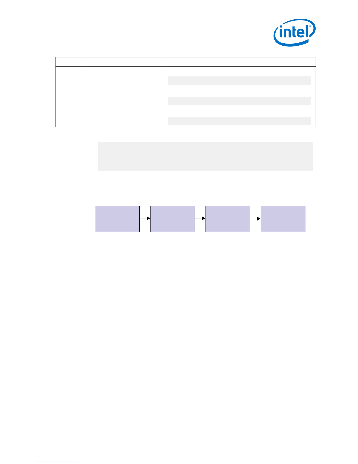
1.3 Generating the Design
Use the Intel FPGA HDMI parameter editor in the Intel Quartus Prime software to
generate the design examples.
Figure 3. Generating the Design Flow
Intel® FPGA HDMI Design Example User Guide for Intel® Arria 10 Devices
7
Page 8
Change to
<Simulator>
Directory
Run
<Simulation Script>
Analyze
Results
1 Intel® FPGA HDMI Design Example Quick Start Guide for Intel® Arria® 10 Devices
UG-20077 | 2017.11.06
1. Create a project targeting Intel Arria 10 device family and select the desired
device.
2. In the IP Catalog, locate and double-click Intel FPGA HDMI IP Core. The New
IP Variant or New IP Variation window appears.
3. Specify a top-level name for your custom IP variation. The parameter editor saves
the IP variation settings in a file named <your_ip>.ip or <your_ip>.qsys.
4. Click OK. The parameter editor appears.
5. On the IP tab, configure the desired parameters for both TX and RX.
6. On the Design Example tab, select Arria 10 HDMI RX-TX Retransmit.
7. Select Simulation to generate the testbench, and select Synthesis to generate
the hardware design example.
You must select at least one of these options to generate the design example files.
If you select both, the generation time is longer.
8. For Generate File Format, select Verilog or VHDL.
9. For Target Development Kit, select Intel Arria 10 GX FPGA Development
Kit. If you select a development kit, then the target device (selected in step 4)
changes to match the device on target board. For Intel Arria 10 GX FPGA
Development Kit, the default device is 10AX115S2F4I1SG.
10. Click Generate Example Design.
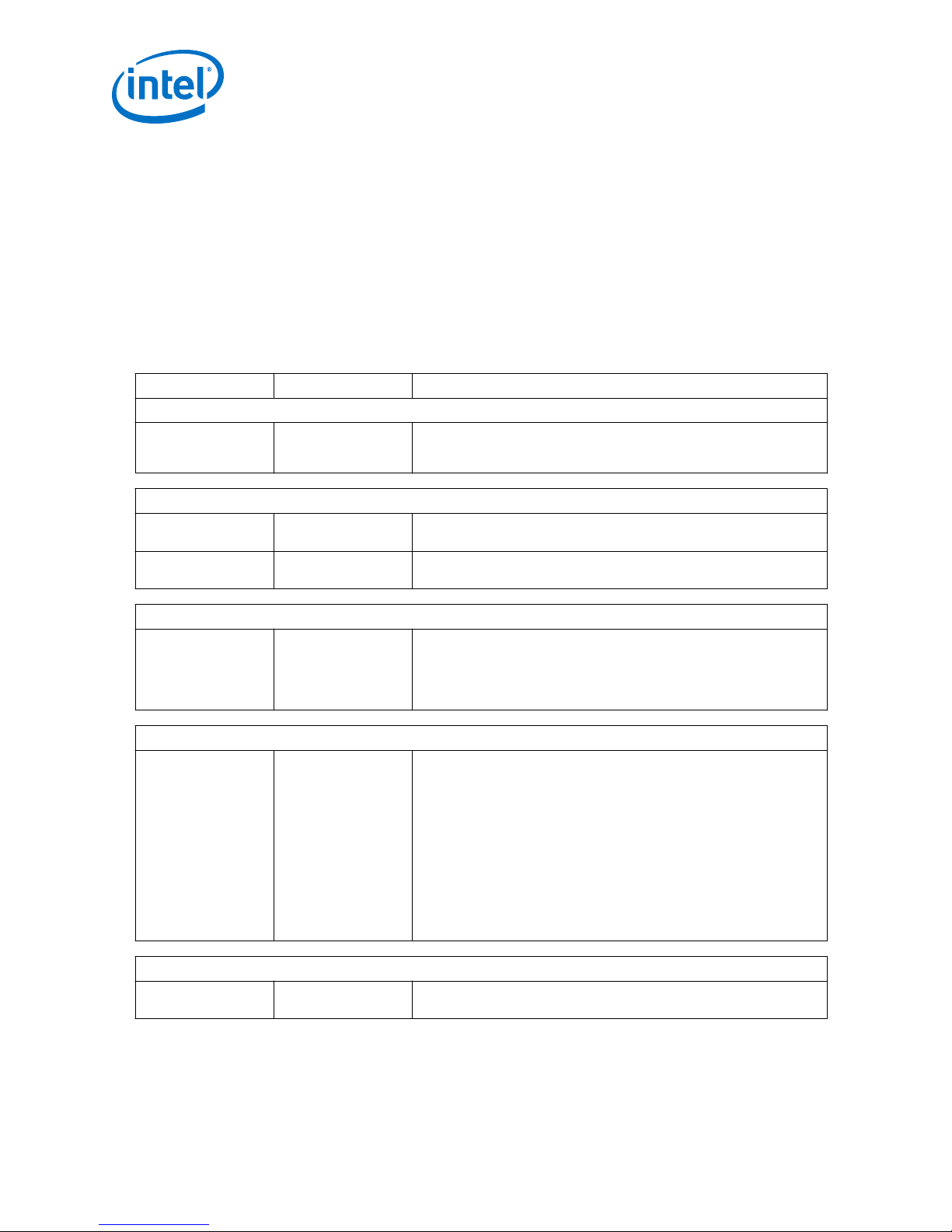
1.4 Simulating the Design
The HDMI testbench simulates a serial loopback design from a TX instance to an RX
instance. Internal video pattern generator and audio pattern generator modules drive
the HDMI TX instance and the serial output from the TX instance connects to the RX
instance in the testbench.
Figure 4. Design Simulation Flow
1. Go to the desired simulation folder.
2. Run the simulation script for the supported simulator of your choice. The script
compiles and runs the testbench in the simulator.
3. Analyze the results.
Table 4. Steps to Run Simulation
Simulator Working Directory Instructions
Riviera-Pro
NCSim
/simulation/aldec
/simulation/cadence
In the command line, type
vsim -c -do aldec.do
In the command line, type
source ncsim.sh
continued...
Intel® FPGA HDMI Design Example User Guide for Intel® Arria 10 Devices
8
Page 9
Compile Design
in Quartus Prime
Software
Set Up Hardware Program Device
Test Design
in Hardware
®
1 Intel
UG-20077 | 2017.11.06
FPGA HDMI Design Example Quick Start Guide for Intel® Arria® 10 Devices
Simulator Working Directory Instructions
ModelSim
/simulation/mentor
In the command line, type
vsim -c -do mentor.do
VCS
VCS-MX
/simulation/synopsys/vcs
/simulation/synopsys/
vcsmx
In the command line, type
source vcs_sim.sh
In the command line, type
source vcsmx_sim.sh
A successful simulation ends with the following message:
# SYMBOLS_PER_CLOCK = 2
# VIC = 0
# AUDIO_CLK_DIVIDE = 800
# TEST_HDMI_6G = 1
# Simulation pass
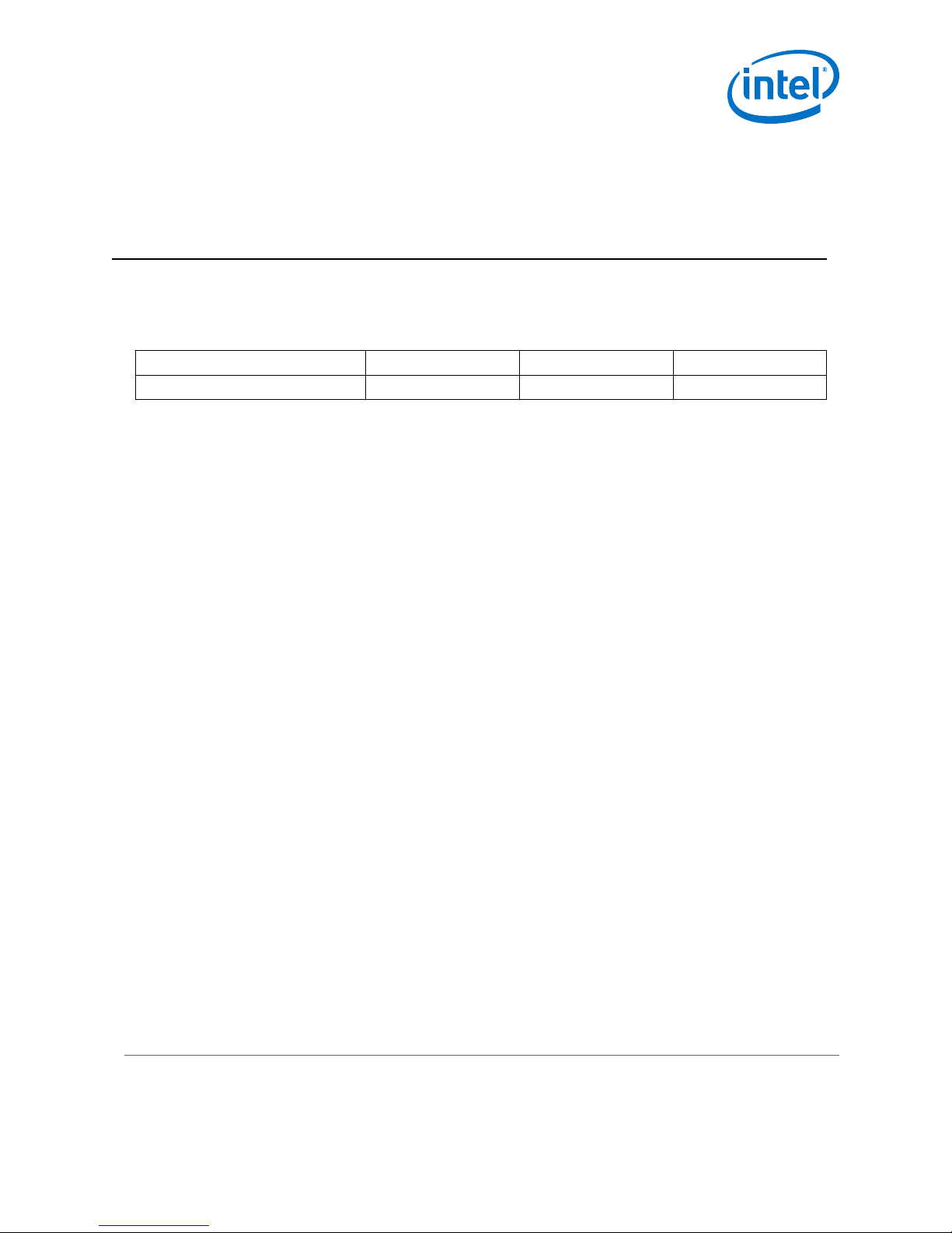
1.5 Compiling and Testing the Design
To compile and run a demonstration test on the hardware example design, follow
these steps:
1. Ensure hardware example design generation is complete.
2. Launch the Intel Quartus Prime software and open project directory/quartus/
a10_hdmi2_demo.qpf.
3.
Click Processing ➤ Start Compilation.
4.
After successful compilation, a .sof file will be generated in your specified
directory.
5. Connect to the on-board FMCB (J2) Bitec HDMI 2.0 FMC Daughter Card Rev 4.
6. Connect TX (P1) of the Bitec HDMI 2.0 FMC Daughter Card (Revision 4) to an
external video source.
7. Connect RX (P2) of the Bitec HDMI 2.0 FMC Daughter Card (Revision 4) to an
external video sink or video analyzer.
8. Ensure all switches on the development board are in default position.
9. Configure the selected Intel Arria 10 device on the development board using the
generated .sof file (Tools ➤ Programmer ).
10. The analyzer should display the video generated from the source.
Related Links
Intel Arria 10 FPGA Development Kit User Guide
Intel® FPGA HDMI Design Example User Guide for Intel® Arria 10 Devices
9
Page 10
1 Intel® FPGA HDMI Design Example Quick Start Guide for Intel® Arria® 10 Devices
UG-20077 | 2017.11.06
1.6 Design Limitation
You may encounter timing violation on the maximum skew constraints required for the
designs that use TX PMA and PCS bonding.
Choose the transceiver channels farther away from the Hard IP (HIP) block to meet
the maximum skew tolerance constraints requirement.
1.7 Intel FPGA HDMI Design Example Parameters
Table 5. Intel FPGA HDMI Design Example Parameters for Intel Arria 10 Devices
These options are available for Intel Arria 10 devices only.
Parameter Value Description
Available Design Example
Select Design Arria 10 HDMI RX-TX
Retransmit
Simulation On, Off Turn on this option to generate the necessary files for the simulation
Synthesis On, Off Turn on this option to generate the necessary files for Intel Quartus
Select the design example to be generated. The generated design
example has preconfigured parameter settings. It does not follow user
settings.
Design Example Files
testbench.
Prime compilation and hardware demonstration.
Generated HDL Format
Generate File Format Verilog, VHDL Select your preferred HDL format for the generated design example
Select Board No Development Kit,
Arria 10 GX FPGA
Development Kit,
Custom Development
Kit
Change Target Device On, Off Turn on this option and select the preferred device variant for the
fileset.
Note: This option only determines the format for the generated top
level IP files. All other files (e.g. example testbenches and top
level files for hardware demonstration) are in Verilog HDL format.
Target Development Kit
Select the board for the targeted design example.
• No Development Kit: This option excludes all hardware aspects for
the design example. The IP core sets all pin assignments to virtual
pins.
• Arria 10 GX FPGA Development Kit: This option automatically selects
the project's target device to match the device on this development
kit. You may change the target device using the Change Target
Device parameter if your board revision has a different device
variant. The IP core sets all pin assignments according to the
development kit.
• Custom Development Kit: This option allows the design example to
be tested on a third party development kit with an Intel FPGA. You
may need to set the pin assignments on your own.
Target Device
development kit.
Intel® FPGA HDMI Design Example User Guide for Intel® Arria 10 Devices
10
Page 11
UG-20077 | 2017.11.06
2 Intel FPGA HDMI Design Example Detailed Description
The Intel FPGA HDMI IP core design example demonstrates one HDMI instance parallel
loopback consisting three RX channels and four TX channels.
Table 6. Intel FPGA HDMI Design Example for Intel Arria 10 Devices
Design Example Data Rate Channel Mode Loopback Type
Arria 10 HDMI RX-TX Retransmit < 6,000 Mbps Simplex Parallel with FIFO buffer
Features
• The design instantiates FIFO buffers to perform a direct HDMI video stream
passthrough between the HDMI sink and source.
• The design uses LED status for early debugging stage.
• The design comes with RX and TX only options.
• The design demonstrates the insertion and filtering of Dynamic Range and
Mastering (HDR) InfoFrame in RX-TX link module.
• The design demonstrates the management of EDID passthrough from an external
HDMI sink to an external HDMI source when triggered by a TX hot-plug event.
• The design uses push-button controlled HDMI TX core signals:
—
mode signal to select DVI or HDMI encoded video frame
—
info_avi[47], info_vsi[61], and audio_info_ai[48] signals to select
auxiliary packet transmission through sidebands or auxiliary data ports
The RX instance receives a video source from the external video generator, and the
data then goes through a loopback FIFO before it is transmitted to the TX instance.
You need to connect an external video analyzer, monitor, or a television with HDMI
connection to the TX core to verify the functionality.
2.1 HDMI RX-TX Retransmit Design Example
The HDMI RX-TX retransmit design example demonstrates parallel loopback on
simplex channel mode for Intel FPGA HDMI IP core.
Intel Corporation. All rights reserved. Intel, the Intel logo, Altera, Arria, Cyclone, Enpirion, MAX, Nios, Quartus
and Stratix words and logos are trademarks of Intel Corporation or its subsidiaries in the U.S. and/or other
countries. Intel warrants performance of its FPGA and semiconductor products to current specifications in
accordance with Intel's standard warranty, but reserves the right to make changes to any products and services
at any time without notice. Intel assumes no responsibility or liability arising out of the application or use of any
information, product, or service described herein except as expressly agreed to in writing by Intel. Intel
customers are advised to obtain the latest version of device specifications before relying on any published
information and before placing orders for products or services.
*Other names and brands may be claimed as the property of others.
ISO
9001:2008
Registered
Page 12
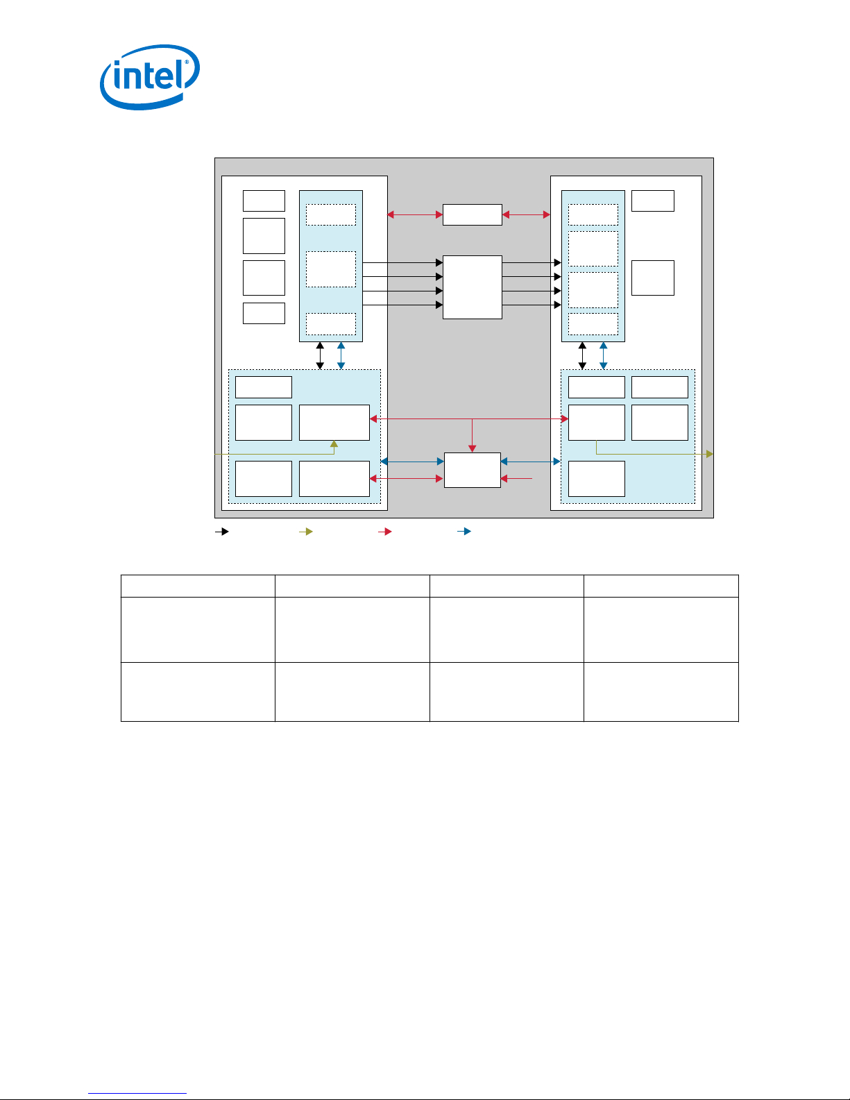
Figure 5. HDMI RX-TX Retransmit
I2C Slave
(EDID)
PIO
I2C Slave
(SCDC)
EDID RAM
RX Core
RX
Oversampler
DCFIFO
RX Core Top
IOPLL
Transceiver PHY
Reset Controller
RX Native PHY
RX Reconfiguration
Management
IOPLL
Reconfiguration
Transceiver
Arbiter
CPU Sub-System
RX-TX Link
I2C
Master
PIO
TX Core
TX
Oversampler
Clock Enable
Generator
DCFIFO
TX Core Top
TX PLL
Transceiver PHY
Reset Controller
TX Native PHY
IOPLL
Reconfiguration
IOPLL
RX Audio
RX Video
RX Auxiliary
RX Sideband
TX Audio
TX Video
TX Auxiliary
TX Sideband
RX Top TX Top
Top
Parallel Data
Serial Data
Avalon-MM
Control and Status
0
2 Intel FPGA HDMI Design Example Detailed Description
UG-20077 | 2017.11.06
To use RX or TX only components, remove the irrelevant blocks from the design
User Requirement
HDMI RX Only RX Top • TX Top
HDMI TX Only TX Top, CPU Sub-System • RX Top
Preserve Remove Add
• RX-TX Link
• CPU Sub-System
• Transceiver Arbiter
• RX-TX Link
• Transceiver Arbiter
—
Video Pattern Generator
(custom module or
generated from the VIP
Suite IP core)
Intel® FPGA HDMI Design Example User Guide for Intel® Arria 10 Devices
12
Page 13
Parallel Data
Serial Data
Avalon-MM
Control and Status
0
Removed RX TX
I2C Slave
(EDID)
PIO
I2C Slave
(SCDC)
EDID RAM
RX Core
RX
Oversampler
DCFIFO
RX Core Top
IOPLL
Transceiver PHY
Reset Controller
RX Native PHY
RX Reconfiguration
Management
IOPLL
Reconfiguration
Transceiver
Arbiter
CPU Sub-System
RX-TX Link
I2C
Master
PIO
TX Core
TX
Oversampler
Clock Enable
Generator
DCFIFO
TX Core Top
TX PLL
Transceiver PHY
Reset Controller
TX Native PHY
IOPLL
Reconfiguration
IOPLL
RX Audio
RX Video
RX Auxiliary
RX Sideband
TX Audio
TX Video
TX Auxiliary
TX Sideband
RX Top TX Top
Top
2 Intel FPGA HDMI Design Example Detailed Description
UG-20077 | 2017.11.06
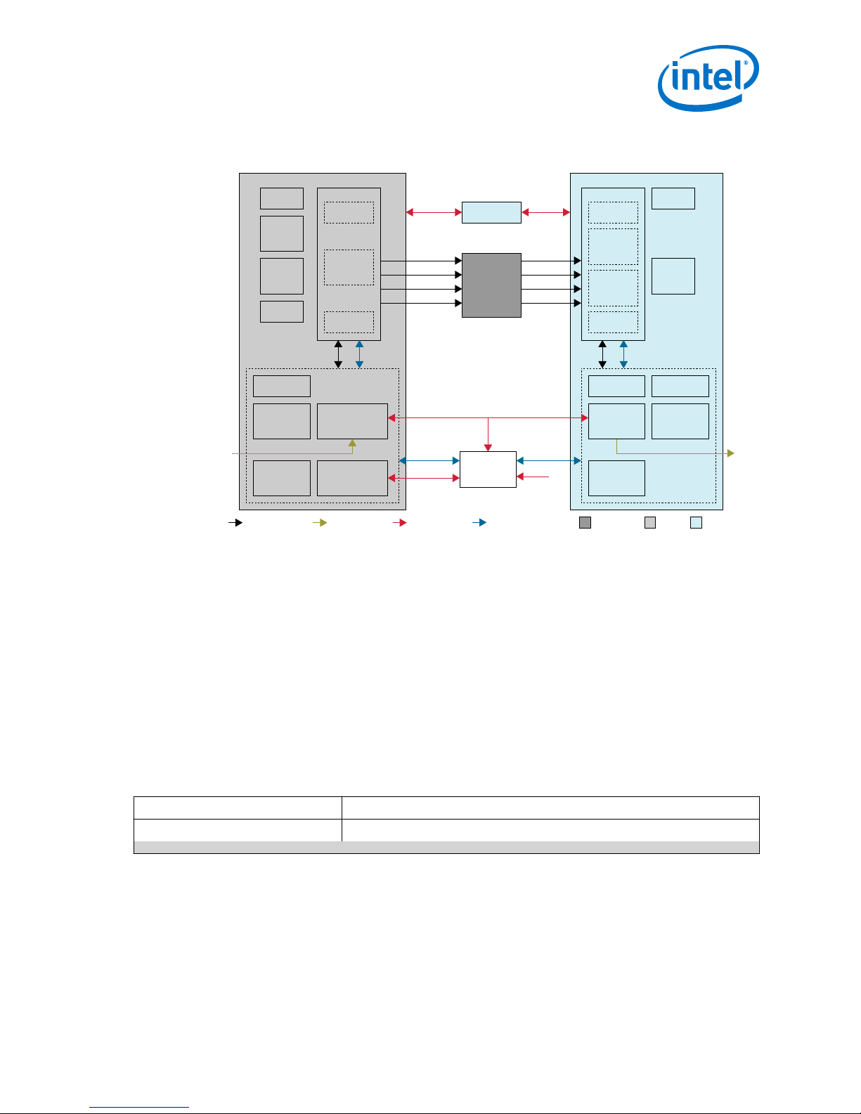
Figure 6. Components Required for RX or TX Only Design
Note: If your design only requires HDMI TX or retransmitting HDMI stream from RX to TX
through video frame buffer, supply the TX PLL reference clock directly from an
external programmable oscillator. Intel recommends that you do not cascade IOPLL to
TX PLL.
Related Links
Jitter of PLL Cascading or Non-Dedicated Clock Path for Arria 10 PLL Reference Clock
Refer to this solution for workaround if your design clocks experience additional
jitter.
2.2 Design Components
Table 7. HDMI RX Top Components
RX Core Top The RX Core top level consists of:
The Intel FPGA HDMI IP core design example requires these components.
Module Description
continued...
Intel® FPGA HDMI Design Example User Guide for Intel® Arria 10 Devices
13
Page 14

2 Intel FPGA HDMI Design Example Detailed Description
UG-20077 | 2017.11.06
Module Description
• HDMI RX Core—The IP core receives the serial data from the Transceiver
Native PHY and performs data alignment, channel deskew, TMDS decoding,
auxiliary data decoding, video data decoding, audio data decoding, and
descrambling.
• RX Oversampler—The RX Oversampler module extracts data from the
oversampled incoming data stream when the detected clock frequency band
is below the transceiver minimum link rate. The oversampling factor is fixed
at 5 and you can program the data width to support different number of
symbols. For Intel Arria 10 devices, the supported data width is 20 bits for 2
symbols per clock. The extracted bit is accompanied by a data valid pulse
asserted every 5 clock cycles.
• DCFIFO —The DCFIFO transfers data from the RX transceiver recovered clock
domain to the RX link speed clock domain.
I2C Slave I2C is the interface used for Sink Display Data Channel (DDC) and Status and
EDID RAM The design stores the EDID information using the RAM 1-port IP core. A standard
IOPLL The IOPLL generates the RX CDR reference clock, link speed clock, and video
Transceiver PHY Reset Controller The Transceiver PHY reset controller ensures a reliable initialization of the RX
RX Native PHY Hard transceiver block that receives the serial data from an external video
RX Reconfiguration Management RX reconfiguration management that implements rate detection circuitry with the
IOPLL Reconfiguration IOPLL reconfiguration block facilitates dynamic real-time reconfiguration of PLLs
Data Channel (SCDC). The HDMI source uses the DDC to determine the
capabilities and characteristics of the sink by reading the Enhanced Extended
Display Identification Data (E-EDID) data structure.
• The 8-bit I2C slave addresses for E-EDID are 0xA0 and 0xA1. The LSB
indicates the access type: 1 for read and 0 for write. When an HPD event
occurs, the I2C slave responds to E-EDID data by reading from the RAM.
• The I2C slave-only controller also supports SCDC for HDMI 2.0 operations.
The 9-bit I2C slave address for the SCDC are 0xA8 and 0xA9. When an HPD
event occurs, the I2C slave performs write or read transaction to or from
SCDC interface of the HDMI RX core.
Note: This I2C slave-only controller for SCDC is not required if HDMI 2.0 is
not intended.
two-wire (clock and data) serial bus protocol (I2C slave-only controller) transfers
the CEA-861-D Compliant E-EDID data structure. This EDID RAM stores the EEDID information.
clock for the incoming TMDS clock.
• Output clock 0 (CDR reference clock)
• Output clock 1 (Link speed clock)
• Output clock 2 (Video clock)
Note: The default IOPLL configuration is not valid for any HDMI resolution. The
IOPLL is reconfigured to the appropriate settings upon power up.
transceivers. The reset input of this controller is triggered by the RX
reconfiguration, and it generates the corresponding analog and digital reset
signal to the Transceiver Native PHY block according to the reset sequencing
inside the block.
source. It deserializes the serial data to parallel data before passing the data to
the HDMI RX core.
HDMI PLL to drive the RX transceiver to operate at any arbitrary link rates
ranging from 250 Mbps to 6,000 Mbps.
Refer to the Multi-Rate Reconfiguration Sequence Flow figure below.
in Intel FPGAs. This block updates the output clock frequency and PLL bandwidth
in real-time, without reconfiguring the entire FPGA. This blocks runs at 100 MHz
in Intel Arria 10 devices.
Due to IOPLL reconfiguration limitation, apply the Quartus INI
permit_nf_pll_reconfig_out_of_lock=on during the IOPLL
reconfiguration IP generation.
continued...
Intel® FPGA HDMI Design Example User Guide for Intel® Arria 10 Devices
14
Page 15

2 Intel FPGA HDMI Design Example Detailed Description
UG-20077 | 2017.11.06
Module Description
To apply the Quartus INI, include
“permit_nf_pll_reconfig_out_of_lock=on” in the quartus.ini file and
place in the file the Intel Quartus Prime project directory. You should see a
warning message when you edit the IOPLL reconfiguration block
(pll_hdmi_reconfig) in the Quartus Prime software with the INI.
Note:
Without this Quartus INI, IOPLL reconfiguration cannot be completed if
the IOPLL loses lock during reconfiguration.
PIO The parallel input/output (PIO) block functions as control, status and reset
interfaces to or from the CPU sub-system.
Intel® FPGA HDMI Design Example User Guide for Intel® Arria 10 Devices
15
Page 16

Reset the RX HDMI PLL and RX transceiver.
Enable the rate detection circuit to measure incoming TMDS clock.
Accept acknowledgement with clock frequency band and desired
RX HDMI PLL and RX transceiver settings.
Determine if RX HDMI PLL and/or RX transceiver reconfiguration
is required based on the previous and current detected clock
frequency band and color depth. Different color depths may fall
within the same clock frequency band.
Request RX HDMI PLL and/or RX transceiver reconfiguration if the
previous and current clock frequency band or color depth differs.
The controller reconfigures the RX HDMI PLL and/or RX transceiver
(followed by recalibration on Intel Arria 10 device).
Reconfiguration Required
Reconfiguration
Not Required
When all reconfiguration processes complete or the previous and
current clock frequency band and color depth do not differ, reset
the RX HDMI PLL and RX transceiver.
Enable rate the detection circuit periodically to monitor the
reference clock frequency. If the clock frequency band changes or
the RX HDMI PLL or RX transceiver or HDMI core lose lock, repeat
the process.
2 Intel FPGA HDMI Design Example Detailed Description
Figure 7. Multi-Rate Reconfiguration Sequence Flow
The figure illustrates the multi-rate reconfiguration sequence flow of the controller when it receivers input data
stream and reference clock frequency, or when the transceiver is unlocked.
UG-20077 | 2017.11.06
Table 8. HDMI TX Top Components
TX Core Top The TX Core top level consists of:
Module Description
continued...
Intel® FPGA HDMI Design Example User Guide for Intel® Arria 10 Devices
16
Page 17

2 Intel FPGA HDMI Design Example Detailed Description
UG-20077 | 2017.11.06
Module Description
• HDMI TX Core—The IP core receives video data from the top level and
performs TMDS encoding, auxiliary data encoding, audio data encoding, video
data encoding, and scrambling.
• TX Oversampler—The TX Oversampler module transmits data by repeating
each bit of the input word a given number of times and constructs the output
words. The oversampling factor can be 3, 4, or 5 depending on the TMDS
clock frequency. The TX oversampler assumes that the input word is only
valid every 3, 4, or 5 clock cycles according to the oversampling factor. This
block is enabled when the outgoing data stream is below the minimum link
rate of the TX transceiver. When FPLL input reference clock frequency is
below 50 MHz, the allowable data rate must be below 1,500 Mbps.
(Refer to Table 9 on page 18.)
• DCFIFO —The DCFIFO transfers data from the TX link speed clock domain to
the transceiver parallel clock out domain. When the Nios II processor
determines the outgoing data stream is below the TX transceiver minimum
data rate, the TX transceiver accepts the data from the TX oversampler.
Otherwise, the TX transceiver reads the data directly from the DCFIFO with a
read request asserted at all times.
• Clock Enable Generator—A logic that generates a clock enable pulse. This
clock enable pulse asserts every 5 clock cycles and serves as a read request
signal to clock the data out from the DCFIFO.
I2C Master I2C is the interface used for Sink Display Data Channel (DDC) and Status and
IOPLL
Transceiver PHY Reset Controller The Transceiver PHY reset controller ensures a reliable initialization of the TX
Transceiver Native PHY Hard transceiver block that receives the parallel data from the HDMI TX core and
Data Channel (SCDC). The HDMI source uses the DDC to determine the
capabilities and characteristics of the sink by reading the Enhanced Extended
Display Identification Data (E-EDID) data structure.
• As DDC, I2C Master reads the EDID from the external sink to configure the
EDID information EDID RAM in the HDMI RX Top or for video processing.
• As SCDC, I2C master transfers the SCDC data structure from the FPGA source
to the external sink for HDMI 2.0 operation. For example, if the outgoing data
stream is above 3,400 Mbps, the Nios II processor commands the I2C master
to update the TMDS_BIT_CLOCK_RATIO and SCRAMBLER_ENABLE bits of
the sink SCDC configuration register to 1.
The IOPLL supplies the link speed clock and video clock from the incoming TMDS
clock.
• Output clock 1 (Link speed clock)
• Output clock 2 (Video clock)
Note: The default IOPLL configuration is not valid for any HDMI resolution. The
IOPLL is reconfigured to the appropriate settings upon power up.
transceivers. The reset input of this controller is triggered from the top level, and
it generates the corresponding analog and digital reset signal to the Transceiver
Native PHY block according to the reset sequencing inside the block.
The tx_ready output signal from this block also functions as a reset signal to
the Intel FPGA HDMI IP core to indicate the transceiver is up and running, and
ready to receive data from the core.
serializes the data from transmitting it.
Reconfiguration interface is enabled in the TX Native PHY block to demonstrate
the connection between TX Native PHY and transceiver arbiter. No
reconfiguration is performed for TX Native PHY.
Note: To meet the HDMI TX inter-channel skew requirement, set the TX channel
bonding mode option in the Intel Arria 10 Transceiver Native PHY
parameter editor to PMA and PCS bonding. You also need to add the
maximum skew (set_max_skew) constraint requirement to the digital
reset signal from the transceiver reset controller (tx_digitalreset) as
recommended in the Intel Arria 10 Transceiver PHY User Guide.
continued...
Intel® FPGA HDMI Design Example User Guide for Intel® Arria 10 Devices
17
Page 18

2 Intel FPGA HDMI Design Example Detailed Description
UG-20077 | 2017.11.06
Module Description
TX PLL The transmitter PLL block provides the serial fast clock to the Transceiver Native
IOPLL Reconfiguration IOPLL reconfiguration block facilitates dynamic real-time reconfiguration of PLLs
PHY block. For this Intel FPGA HDMI design example, fPLL is used as TX PLL.
in Intel FPGAs. This block updates the output clock frequency and PLL bandwidth
in real-time, without reconfiguring the entire FPGA. This blocks runs at 100 MHz
in Intel Arria 10 devices.
Due to IOPLL reconfiguration limitation, apply the Quartus INI
permit_nf_pll_reconfig_out_of_lock=on during the IOPLL
reconfiguration IP generation.
To apply the Quartus INI, include
“permit_nf_pll_reconfig_out_of_lock=on” in the quartus.ini file and
place in the file the Intel Quartus Prime project directory. You should see a
warning message when you edit the IOPLL reconfiguration block
(pll_hdmi_reconfig) in the Quartus Prime software with the INI.
Note:
Without this Quartus INI, IOPLL reconfiguration cannot be completed if
the IOPLL loses lock during reconfiguration.
PIO The parallel input/output (PIO) block functions as control, status and reset
interfaces to or from the CPU sub-system.
Table 9. Transceiver Data Rate and Oversampling Factor for Each TMDS Clock
Frequency Range
TMDS Clock Frequency
(MHz)
85–150 1 Not applicable 3400–6000
100–340 0 Not applicable 1000–3400
50–100 0 5 2500–5000
35–50 0 3 1050–1500
30–35 0 4 1200–1400
25–30 0 5 1250–1500
TMDS Bit clock Ratio Oversampling Factor Transceiver Data Rate (Mbps)
Table 10. Top-Level Common Blocks
Module Description
Transceiver Arbiter This generic functional block prevents transceivers from recalibrating
simultaneously when either RX or TX transceivers within the same physical
channel require reconfiguration. The simultaneous recalibration impacts
applications where RX and TX transceivers within the same channel are assigned
to independent IP implementations.
This transceiver arbiter is an extension to the resolution recommended for
merging simplex TX and simplex RX into the same physical channel. This
transceiver arbiter also assists in merging and arbitrating the Avalon-MM RX and
TX reconfiguration requests targeting simplex RX and TX transceivers within a
channel as the reconfiguration interface port of the transceivers can only be
accessed sequentially.
The interface connection between the transceiver arbiter and TX/RX Native
PHY/PHY Reset Controller blocks in this design example demonstrates a generic
mode that apply for any IP combination using the transceiver arbiter. The
transceiver arbiter is not required when only either RX or TX transceiver is used
in a channel.
The transceiver arbiter identifies the requester of a reconfiguration through its
Avalon-MM reconfiguration interfaces and ensures that the corresponding
tx_reconfig_cal_busy or rx_reconfig_cal_busy is gated accordingly.
continued...
Intel® FPGA HDMI Design Example User Guide for Intel® Arria 10 Devices
18
Page 19

2 Intel FPGA HDMI Design Example Detailed Description
UG-20077 | 2017.11.06
Module Description
For HDMI application, only RX initiates reconfiguration. By channeling the
Avalon-MM reconfiguration request through the arbiter, the arbiter identifies that
the reconfiguration request originates from the RX, which then gates
tx_reconfig_cal_busy from asserting and allows rx_reconfig_cal_busy
to assert. The gating prevents the TX transceiver from being moved to
calibration mode unintentionally.
Note: Because HDMI only requires RX reconfiguration, the
tx_reconfig_mgmt_* signals are tied off. Also, the Avalon-MM interface
is not required between the arbiter and the TX Native PHY block. The
blocks are assigned to the interface in the design example to demonstrate
generic transceiver arbiter connection to TX/RX Native PHY/PHY Reset
Controller.
RX-TX Link • The video data output and synchronization signals from HDMI RX core loop
CPU Sub-System The CPU sub-system functions as SCDC and DDC controllers, and source
through a DCFIFO across the RX and TX video clock domains.
• The General Control Packet (GCP), InfoFrames (AVI, VSI and AI), auxiliary
data, and audio data loop through DCFIFOs across the RX and TX link speed
clock domains.
• The auxiliary data port of the HDMI TX core controls the auxiliary data that
flow through the DCFIFO through backpressure. The backpressure ensures
there is no incomplete auxiliary packet on the auxiliary data port.
• This block also performs external filtering:
— Filters the audio data and audio clock regeneration packet from the
auxiliary data stream before transmitting to the HDMI TX core auxiliary
data port.
Note:
To disable this filtering, press user_pb[2]. Enable this filtering to
ensure there is no duplication of audio data and audio clock
regeneration packet in the retransmitted auxiliary data stream.
— Filters the High Dynamic Range (HDR) Infoframe from the HDMI RX
auxiliary data and inserts an example HDR Infoframe to the auxiliary data
of the HDMI TX through the Avalon ST multiplexer.
reconfiguration controller.
• The source SCDC controller contains the I2C master controller. The I2C
master controller transfers the SCDC data structure from the FPGA source to
the external sink for HDMI 2.0 operation. For example, if the outgoing data
stream is 6,000 Mbps, the Nios II processor commands the I2C master
controller to update the TMDS_BIT_CLOCK_RATIO and SCRAMBLER_ENABLE
bits of the sink TMDS configuration register to 1.
• The same I2C master also transfers the DDC data structure (E-EDID) between
the HDMI source and external sink.
• The Nios II CPU acts as the reconfiguration controller for the HDMI source.
The CPU relies on the periodic rate detection from the RX Reconfiguration
Management module to determine if the TX requires reconfiguration. The
Avalon-MM slave translator provides the interface between the Nios II
processor Avalon-MM master interface and the Avalon-MM slave interfaces of
the externally instantiated HDMI source’s IOPLL and TX Native PHY.
• The reconfiguration sequence flow for TX is same as RX, except that the PLL
and transceiver reconfiguration and the reset sequence is performed
sequentially. Refer to Figure 8 on page 20.
Intel® FPGA HDMI Design Example User Guide for Intel® Arria 10 Devices
19
Page 20

Figure 8. Reconfiguration Sequence Flow
The Nios II processor commands the I C master
to send SCDC information.
Reconfiguration Required
Measure Valid Received A TX Hot-Plug Event Occured
Reconfiguration
Not Required
Poll periodic measure valid signal from RX rata detection circuit to determine
whether TX reconfiguration is required. Also, poll the TX hot-plug request to
determine whether a TX hot-plug event has occured.
Reset the TX HDMI PLL and TX transceiver. Initialize the I C Master Controller Core.
2
Retrieve the clock frequency band based on
the measure and TMDS_Bit_clock_Ratio
values and read the color depth information
from the HDMI sink to determine whether
TX HDMI PLL and TX transceiver
reconfiguration and oversampling is required.
Read TMDS_Bit_clock_Ratio value from
the HDMI sink and measure value.
Nios II processor sends sequential commands
to reconfigure the TX HDMI PLL and TX
transceiver (followed by recalibration on
Intel Arria 10 device), and reset sequence after
reconfiguration. It then sends a reset to the
HDMI TX core.
Deassert edid_ram_access control signal
to enable the HDMI RX Top to trigger a
hotplug detect event to the external
HDMI source.
Assert HDMI RX Top’s edid_ram_access
control signal to block HDMI sink’s EDID
RAM from being accessed by external
HDMI source.
Send TMDS_Bit_clock_Ratio and
Scrambler_Enable information to the
external HDMI sink’s SCDC registers
through the I C interface.
2
Read EDID from external sink through I C
interface and write the EDID content to
the HDMI RX EDID RAM.
2
2
The figure illustrates the Nios II software flow that involves the controls for I2C master and HDMI source.
2 Intel FPGA HDMI Design Example Detailed Description
UG-20077 | 2017.11.06
2.3 Dynamic Range and Mastering (HDR) InfoFrame Insertion and
Filtering
The Intel FPGA HDMI design example includes a demonstration of HDR Infoframe
insertion in a RX-TX loopback system.
HDMI Specification version 2.0a allows Dynamic Range and Mastering InfoFrame to be
transmitted through HDMI auxiliary stream. In the demonstration, the Auxiliary Data
Insertion block supports the HDR insertion. You only need to format the intended HDR
Infoframe packet as specified in the module’s signal list table and use the provided
AUX Insertion Control module to schedule the insertion of the HDR infoframe once
every video frame.
In this example configuration, in instances where the incoming auxiliary stream
already includes HDR Infoframe, the streamed HDR content is filtered. The filtering
avoids conflicting HDR Infoframes to be transmitted and ensures that only the values
specified in the HDR Sample Data module are used.
Intel® FPGA HDMI Design Example User Guide for Intel® Arria 10 Devices
20
Page 21

HDMI RX
Top
HDMI TX
Top
Auxiliary
Packet Filter
Video
Bypass FIFO
Audio
Bypass FIFO
Sideband
Bypass FIFO
Auxiliary
Bypass FIFO
Auxiliary
Packet
Generator
Multiplexer
In1
In0
HDR
Data
AUX
Insertion
Control
Auxiliary Data Insertion Block
Auxiliary Data Interface
Auxiliary InfoFrame
Content Interface
Auxiliary Insertion
Control Interface
block_ext_hdr_infoframe
RX Video
TX Video
RX Audio
TX Audio
RX Sideband
TX Sideband
RX Auxiliary
TX Auxiliary
RX-TX Link
2 Intel FPGA HDMI Design Example Detailed Description
UG-20077 | 2017.11.06
Figure 9. RX-TX Link with Dynamic Range and Mastering InfoFrame Insertion
The figure shows the block diagram of RX-TX link including Dynamic Range and Mastering InfoFrame insertion
into the HDMI TX core auxiliary stream.
Table 11. Auxiliary Data Insertion Block (altera_hdmi_aux_hdr) Signals
Signal Direction Width Description
Clock and Reset
Input 1 Clock input. This clock should be
Input 1 Reset input.
Output 72 Avalon streaming output from
Output 1
Output 1
Output 1
Output 1
Output 11
Input 72 Avalon streaming input to the
Input 1
Input 1
Input 1
Input 1
clk_clk
reset_reset_n
multiplexer_out_data
multiplexer_out_valid
multiplexer_out_ready
multiplexer_out_startofpacket
multiplexer_out_endofpacket
multiplexer_out_channel
multiplexer_in_data
multiplexer_in_valid
multiplexer_in_ready
multiplexer_in_startofpacket
multiplexer_in_endofpacket
Auxiliary Packet Generator and Multiplexer Signals
connected to the link speed
clock.
the multiplexer.
In1 port of the multiplexer.
Intel® FPGA HDMI Design Example User Guide for Intel® Arria 10 Devices
21
Page 22

2 Intel FPGA HDMI Design Example Detailed Description
Control Signal
hdmi_tx_vsync
Input 1 HDMI TX Video Vsync. This
Table 12. HDR Data Module (altera_hdmi_hdr_infoframe) Signals
Signal Direction Width Description
hb0
hb1
hb2
pb
Output 8 Header byte 0 of the Dynamic
Output 8 Header byte 1 of the Dynamic
Output 8 Header byte 2 of the Dynamic
Input 224 Data byte of the Dynamic Range
UG-20077 | 2017.11.06
signal should be synchronized to
the link speed clock domain.
The core inserts the HDR
InfoFrame to the auxiliary
stream at the rising edge of this
signal.
Range and Mastering
InfoFrame: InfoFrame type
code.
Range and Mastering
InfoFrame: InfoFrame version
number.
Range and Mastering
InfoFrame: Length of
InfoFrame.
and Mastering InfoFrame.
Table 13. Dynamic Range and Mastering InfoFrame Data Byte Bundle Bit-Fields
Bit-Field Definition Static Metadata Type 1
7:0 Data Byte 1: {5'h0, EOTF[2:0]}
15:8 Data Byte 2: {5'h0, Static_Metadata_Descriptor_ID[2:0]}
23:16 Data Byte 3: Static_Metadata_Descriptor display_primaries_x[0], LSB
31:24 Data Byte 4: Static_Metadata_Descriptor display_primaries_x[0], MSB
39:32 Data Byte 5: Static_Metadata_Descriptor display_primaries_y[0], LSB
47:40 Data Byte 6: Static_Metadata_Descriptor display_primaries_y[0], MSB
55:48 Data Byte 7: Static_Metadata_Descriptor display_primaries_x[1], LSB
63:56 Data Byte 8: Static_Metadata_Descriptor display_primaries_x[1], MSB
71:64 Data Byte 9: Static_Metadata_Descriptor display_primaries_y[1], LSB
79:72 Data Byte 10: Static_Metadata_Descriptor display_primaries_y[1], MSB
87:80 Data Byte 11: Static_Metadata_Descriptor display_primaries_x[2], LSB
95:88 Data Byte 12: Static_Metadata_Descriptor display_primaries_x[2], MSB
103:96 Data Byte 13: Static_Metadata_Descriptor display_primaries_y[2], LSB
111:104 Data Byte 14: Static_Metadata_Descriptor display_primaries_y[2], MSB
119:112 Data Byte 15: Static_Metadata_Descriptor white_point_x, LSB
127:120 Data Byte 16: Static_Metadata_Descriptor white_point_x, MSB
135:128 Data Byte 17: Static_Metadata_Descriptor white_point_y, LSB
continued...
Intel® FPGA HDMI Design Example User Guide for Intel® Arria 10 Devices
22
Page 23

2 Intel FPGA HDMI Design Example Detailed Description
UG-20077 | 2017.11.06
Bit-Field Definition Static Metadata Type 1
143:136 Data Byte 18: Static_Metadata_Descriptor white_point_y, MSB
151:144 Data Byte 19: Static_Metadata_Descriptor max_display_mastering_luminance, LSB
159:152 Data Byte 20: Static_Metadata_Descriptor max_display_mastering_luminance, MSB
167:160 Data Byte 21: Static_Metadata_Descriptor min_display_mastering_luminance, LSB
175:168 Data Byte 22: Static_Metadata_Descriptor min_display_mastering_luminance, MSB
183:176 Data Byte 23: Static_Metadata_Descriptor Maximum Content Light Level, LSB
191:184 Data Byte 24: Static_Metadata_Descriptor Maximum Content Light Level, MSB
199:192 Data Byte 25: Static_Metadata_Descriptor Maximum Frame-average Light Level,
207:200 Data Byte 26: Static_Metadata_Descriptor Maximum Frame-average Light Level,
215:208 Reserved
223:216 Reserved
LSB
MSB
Disabling HDR Insertion and Filtering
Disabling HDR insertion and filter enables you to verify the retransmission of HDR
content already available in the source auxiliary stream without any modification in
the RX-TX Retransmit design example.
To disable HDR Infoframe insertion and filtering:
1.
Set block_ext_hdr_infoframe to 1’b0 in the rxtx_link.v file to prevent
the filtering of the HDR Infoframe from the Auxiliary stream.
2.
Set multiplexer_in0_valid of the avalon_st_multiplexer instance in the
altera_hdmi_aux_hdr.v file to 1'b0 to prevent the Auxiliary Packet Generator
from forming and inserting additional HDR Infoframe into the TX Auxiliary stream.
2.4 Clocking Scheme
The clocking scheme illustrates the clock domains in the Intel FPGA HDMI IP core
design example.
Intel® FPGA HDMI Design Example User Guide for Intel® Arria 10 Devices
23
Page 24

I2C Slave
(EDID)
PIO
I2C Slave
(EDID)
EDID RAM
RX Core
RX
Oversampler
DCFIFO
RX Core Top
IOPLL
Transceiver PHY
Reset Controller
RX Native PHY
RX Reconfiguration
Management
IOPLL
Reconfiguration
Transceiver
Arbiter
CPU Sub-System
RX-TX Link
I2C
Master
PIO
TX Core
TX
Oversampler
DCFIFO
TX Core Top
TX PLL
Transceiver PHY
Reset Controller
TX Native PHY
IOPLL
Reconfiguration
IOPLL
RX Top TX Top
Top
RX Transceiver Clock Out
RX Link Speed Clock
RX Video Clock
RX CDR Reference Clock
TX PLL Serial Clock Management Clock
I2C Clock
RX TMDS Clock
TX IOPLL/TX PLL Reference Clock
TX Transceiver Clock Out
TX Link Speed Clock
TX Video Clock
Clock Enable
Generator
2 Intel FPGA HDMI Design Example Detailed Description
Figure 10. Intel FPGA HDMI Design Example Clocking Scheme
UG-20077 | 2017.11.06
Table 14. Clocking Scheme Signals
Clock Signal Name in Design Description
TX IOPLL/ TX PLL Reference
Clock
TX Transceiver Clock Out
TX/RX Link Speed Clock
TX PLL Serial Clock
hdmi_clk_in
tx_clk
tx_bonding_clocks
ls_clk
Reference clock to the TX IOPLL and TX PLL. The clock
frequency is the same as the expected TMDS clock
frequency from the HDMI TX TMDS clock channel.
For this Intel FPGA HDMI design example, this clock is
connected to the RX TMDS clock for demonstration purpose.
In your application, you need to supply a dedicated clock
with TMDS clock frequency from a programmable oscillator
for better jitter performance.
Note:
Do not use a transceiver RX pin as a TX PLL
reference clock. Your design will fail to fit if you
place the HDMI TX refclk on an RX pin.
Clock out recovered from the transceiver, and the frequency
varies depending on the data rate and symbols per clock.
TX transceiver clock out frequency = Transceiver data rate/
(Symbol per clock*10)
Serial fast clock generated by TX PLL. The clock frequency is
set based on the data rate.
Link speed clock. The link speed clock frequency depends
on the expected TMDS clock frequency, oversampling factor,
symbols per clock, and TMDS bit clock ratio.
continued...
Intel® FPGA HDMI Design Example User Guide for Intel® Arria 10 Devices
24
Page 25

2 Intel FPGA HDMI Design Example Detailed Description
UG-20077 | 2017.11.06
Clock Signal Name in Design Description
TMDS Bit Clock Ratio Link Speed Clock Frequency
0 TMDS clock frequency/ Symbol
per clock
1 TMDS clock frequency *4 /
Symbol per clock
TX/RX Video Clock
RX TMDS Clock
RX CDR Reference Clock
vid_clk
tmds_clk_in
iopll_outclk0
Video data clock. The video data clock frequency is derived
from the TX link speed clock based on the color depth.
TMDS Bit Clock Ratio Video Data Clock Frequency
0 TMDS clock/ Symbol per clock/
1 TMDS clock *4 / Symbol per
Bits per Color Color Depth Factor
8 1
10 1.25
12 1.5
16 2.0
TMDS clock channel from the HDMI RX and connects to the
reference clock to the IOPLL.
Reference clock to the RX CDR of RX transceiver.
Data Rate RX Reference Clock
Data rate <1 Gbps 5× TMDS clock frequency
1 Gbps< Data rate
<3.4 Gbps
Data rate >3.4 Gbps 4× TMDS clock frequency
Color depth factor
clock/ Color depth factor
Frequency
TMDS clock frequency
RX Transceiver Clock Out
Management Clock
rx_clk
mgmt_clk
• Data Rate <1 Gbps: For oversampling to meet
transceiver minimum data rate requirement.
• Data Rate >3.4 Gbps: To compensate for the TMDS bit
rate to clock ratio of 1/40 to maintain the transceiver
data rate to clock ratio at 1/10.
Note:
Do not use a transceiver RX pin as a CDR reference
clock. Your design will fail to fit if you place the
HDMI RX refclk on an RX pin.
Clock out recovered from the transceiver, and the frequency
varies depending on the data rate and symbols per clock.
RX transceiver clock out frequency = Transceiver data rate/
(Symbol per clock*10)
A free running 100 MHz clock for these components:
continued...
Intel® FPGA HDMI Design Example User Guide for Intel® Arria 10 Devices
25
Page 26

Clock Signal Name in Design Description
I2C Clock
Related Links
• Using Transceiver RX Pin as CDR Reference Clock
• Using Transceiver RX Pin as TX PLL Reference Clock
2.5 Interface Signals
i2c_clk
2 Intel FPGA HDMI Design Example Detailed Description
UG-20077 | 2017.11.06
• AVMM interfaces for reconfiguration
The frequency range requirement is between 100–125
MHz.
• PHY reset controller for transceiver reset sequence
The frequency range requirement is between 1–500
MHz.
• IOPLL Reconfiguration
Maximum clock frequency is 100 MHz.
• RX Reconfiguration for management
• CPU
• I2C Master
A 50 MHz clock input that clocks I2C slave, SCDC registers
in the HDMI RX core, and EDID RAM.
The tables list the signals for the Intel FPGA HDMI IP core design example.
Table 15. Top-Level Signals
Signal Direction Width Description
clk_fpga_b3_p
clk_50
user_pb
cpu_resetn
user_led_g
user_led_r
fmcb_gbtclk_m2c_p_0
fmcb_dp_m2c_p
fmcb_dp_c2m_p
fmcb_la_rx_p_9
fmcb_la_rx_p_8
fmcb_la_rx_n_8
On-board Oscillator Signal
Input 1 100 MHz free running clock
Input 1 50 MHz free running clock
User Push Buttons and LEDs
Input 1 Push button to control the Intel FPGA
HDMI design functionality
Input 1 Global reset
Output 8 Green LED display
Output 8 Red LED display
HDMI FMC Daughter Card Pins on FMC Port B
Input 1 HDMI RX TMDS clock
Input 3 HDMI RX red, green, and blue data
channels
Output 4 HDMI TX clock, red, green, and blue data
channels
Input 1 HDMI RX +5V power detect
Inout 1 HDMI RX hot plug detect
Inout 1 HDMI RX I2C SDA
continued...
Intel® FPGA HDMI Design Example User Guide for Intel® Arria 10 Devices
26
Page 27

2 Intel FPGA HDMI Design Example Detailed Description
UG-20077 | 2017.11.06
HDMI FMC Daughter Card Pins on FMC Port B
fmcb_la_tx_p_10
fmcb_la_tx_p_12
fmcb_la_tx_n_12
fmcb_la_rx_p_10
Input 1 HDMI RX I2C SCL
Input 1 HDMI TX hot plug detect
Inout 1 HDMI I2C SDA
Inout 1 HDMI I2C SCL
Table 16. HDMI RX Top-Level Signals
Signal Direction Width Description
Clock and Reset Signals
mgmt_clk
reset
tmds_clk_in
i2c_clk
vid_clk_out
ls_clk_out
sys_init
Input 1 System clock input (100 MHz)
Input 1 System reset input
Input 1 HDMI RX TMDS clock
Input 1 Clock input for DDC and SCDC interface
Output 1 Video clock output
Output 8 Link speed clock output
Output 1 System initialization to reset the system
upon power-up
rx_serial_data
gxb_rx_ready
gxb_rx_cal_busy_out
gxb_rx_cal_busy_in
iopll_locked
gxb_reconfig_write
gxb_reconfig_read
gxb_reconfig_address
gxb_reconfig_writedata
gxb_reconfig_readdata
gxb_reconfig_waitrequest
rx_reconfig_en
measure
measure_valid
os
RX Transceiver and IOPLL Signals
Input 3 HDMI serial data to the RX Native PHY
Output 1 Indicates RX Native PHY is ready
Output 3 RX Native PHY calibration busy to the
Input 3 Calibration busy signal from the
Output 1 Indicate IOPLL is locked
Input 3 Transceiver reconfiguration Avalon-MM
Input 3
Input 30
Input 96
Output 96
Output 3
RX Reconfiguration Management
Output 1 RX Reconfiguration enables signal
Output 24 HDMI RX TMDS clock frequency
Output 1 Indicates the measure signal is valid
Output 1 Oversampling factor:
transceiver arbiter
transceiver arbiter to the RX Native PHY
interface from the RX Native PHY to the
transceiver arbiter
measurement (in 10 ms)
continued...
Intel® FPGA HDMI Design Example User Guide for Intel® Arria 10 Devices
27
Page 28

reconfig_mgmt_write
reconfig_mgmt_read
reconfig_mgmt_address
reconfig_mgmt_writedata
reconfig_mgmt_readdata
reconfig_mgmt_waitrequest
TMDS_Bit_clock_Ratio
audio_de
audio_data
audio_info_ai
audio_N
audio_CTS
audio_metadata
audio_format
aux_pkt_data
aux_pkt_addr
aux_pkt_wr
aux_data
aux_sop
aux_eop
aux_valid
aux_error
gcp
info_avi
info_vsi
colordepth_mgmt_sync
vid_data
vid_vsync
vid_hsync
vid_de
mode
2 Intel FPGA HDMI Design Example Detailed Description
UG-20077 | 2017.11.06
RX Reconfiguration Management
• 0: No oversampling
• 1: 5× oversampling
Output 1 RX reconfiguration management Avalon-
Output 1
Output 12
Output 32
Input 32
Input 1
HDMI RX Core Signals
Output 1 SCDC register interfaces
Output 1 HDMI RX core audio interfaces
Output 256
Output 48
Output 20
Output 20
Output 165
Output 5
Output 72 HDMI RX core auxiliary interfaces
Output 6
Output 1
Output 72
Output 1
Output 1
Output 1
Output 1
Output 6 HDMI RX core sideband signals
Output 112
Output 61
Output 2
Output N*48 HDMI RX core video ports
Output N
Output N
Output N
Output 1 HDMI RX core control and status ports
MM interface to transceiver arbiter
Note: N = symbols per clock
continued...
Intel® FPGA HDMI Design Example User Guide for Intel® Arria 10 Devices
28
Page 29

2 Intel FPGA HDMI Design Example Detailed Description
UG-20077 | 2017.11.06
HDMI RX Core Signals
ctrl
locked
vid_lock
in_5v_power
hdmi_rx_hpd_n
hdmi_rx_i2c_sda
hdmi_rx_i2c_scl
edid_ram_access
edid_ram_address
edid_ram_write
edid_ram_read
edid_ram_readdata
edid_ram_writedata
edid_ram_waitrequest
Output N*6 Note: N = symbols per clock
Output 3
Output 1
Input 1 HDMI RX 5V detect and hotplug detect
Inout 1
Inout 1 HDMI RX DDC and SCDC interface
Inout 1
RX EDID RAM Signals
Input 1 HDMI RX EDID RAM access interface.
Input 8
Input 1
Input 1
Output 8
Input 8
Output 1
I2C Signals
Assert edid_ram_access when you want
to write or read from the EDID RAM, else
this signal should be kept low.
Table 17. HDMI TX Top-Level Signals
Signal Direction Width Description
Clock and Reset Signals
mgmt_clk
reset
hdmi_clk_in
vid_clk_out
ls_clk_out
sys_init
reset_xcvr
reset_pll
reset_pll_reconfig
TX Transceiver and IOPLL Signals
tx_serial_data
gxb_tx_ready
Input 1 System clock input (100 MHz)
Input 1 System reset input
Input 1 Reference clock to TX IOPLL and TX PLL.
The clock frequency is the same as the
TMDS clock frequency.
Output 1 Video clock output
Output 8 Link speed clock output
Output 1 System initialization to reset the system
upon power-up
Input 1 Reset to TX transceiver
Input 1 Reset to IOPLL and TX PLL
Output 1 Reset to PLL reconfiguration
Output 4 HDMI serial data from the TX Native PHY
Output 1 Indicates TX Native PHY is ready
continued...
Intel® FPGA HDMI Design Example User Guide for Intel® Arria 10 Devices
29
Page 30

gxb_tx_cal_busy_out
gxb_tx_cal_busy_in
iopll_locked
txpll_locked
gxb_reconfig_write
gxb_reconfig_read
gxb_reconfig_address
gxb_reconfig_writedata
gxb_reconfig_readdata
gxb_reconfig_waitrequest
pll_reconfig_write/
tx_pll_reconfig_write
pll_reconfig_read/
tx_pll_reconfig_read
pll_reconfig_address/
tx_pll_reconfig_address
pll_reconfig_writedata/
tx_pll_reconfig_writedata
pll_reconfig_readdata/
tx_pll_reconfig_readdata
pll_reconfig_waitrequest/
tx_pll_reconfig_waitrequest
os
measure
2 Intel FPGA HDMI Design Example Detailed Description
TX Transceiver and IOPLL Signals
Output 4 TX Native PHY calibration busy signal to
Input 4 Calibration busy signal from the
Output 1 Indicate IOPLL is locked
Output 1 Indicate TX PLL is locked
Input 4 Transceiver reconfiguration Avalon-MM
Input 4
Input 40
Input 128
Output 128
Output 4
TX IOPLL and TX PLL Reconfiguration Signals
Input 1 TX IOPLL/TX PLL reconfiguration Avalon-
Input 1
Input 10
Input 32
Output 32
Output 1
Input 2 Oversampling factor:
Input 24 Indicates the TMDS clock frequency of the
the transceiver arbiter
transceiver arbiter to the TX Native PHY
interface from the TX Native PHY to the
transceiver arbiter
MM interfaces
• 0: No oversampling
• 1: 3× oversampling
• 2: 4× oversampling
• 3: 5× oversampling
transmitting video resolution.
UG-20077 | 2017.11.06
ctrl
mode
TMDS_Bit_clock_Ratio
Scrambler_Enable
audio_de
audio_mute
Intel® FPGA HDMI Design Example User Guide for Intel® Arria 10 Devices
30
HDMI TX Core Signals
Input 6*N HDMI TX core control interfaces
Input 1
Input 1 SCDC register interfaces
Input 1
Input 1 HDMI TX core audio interfaces
Input 1
Note: N = Symbols per clock
continued...
Page 31

2 Intel FPGA HDMI Design Example Detailed Description
UG-20077 | 2017.11.06
HDMI TX Core Signals
audio_data
audio_info_ai
audio_N
audio_CTS
audio_metadata
audio_format
aux_ready
aux_data
aux_sop
aux_eop
aux_valid
gcp
info_avi
info_vsi
vid_data
vid_vsync
vid_hsync
vid_de
Input 256
Input 49
Input 22
Input 22
Input 166
Input 5
Output 1 HDMI TX core auxiliary interfaces
Input 72
Input 1
Input 1
Input 1
Input 6 HDMI TX core sideband signals
Input 113
Input 62
Input N*48 HDMI TX core video ports
Input N
Input N
Input N
Note: N = symbols per clock
tx_i2c_avalon_waitrequest
tx_i2c_avalon_address
tx_i2c_avalon_writedata
tx_i2c_avalon_readdata
tx_i2c_avalon_chipselect
tx_i2c_avalon_write
tx_i2c_avalon_irq
hdmi_tx_i2c_sda
hdmi_tx_i2c_scl
hdmi_tx_hpd_n
tx_hpd_ack
tx_hpd_req
I2C and Hot Plug Detect Signals
Output 1 I2C master Avalon-MM interfaces
Input 3
Input 32
Output 32
Input 1
Input 1
Output 1
Inout 1 HDMI TX DDC and SCDC interfaces
Inout 1
Input 1 HDMI TX hotplug detect interfaces
Input 1
Output 1
Intel® FPGA HDMI Design Example User Guide for Intel® Arria 10 Devices
31
Page 32

Table 18. Transceiver Arbiter Signals
Signal Direction Width Description
clk
reset
rx_rcfg_en
tx_rcfg_en
rx_rcfg_ch
tx_rcfg_ch
rx_reconfig_mgmt_write
rx_reconfig_mgmt_read
rx_reconfig_mgmt_address
rx_reconfig_mgmt_writedata
rx_reconfig_mgmt_readdata
rx_reconfig_mgmt_waitrequest
tx_reconfig_mgmt_write
tx_reconfig_mgmt_read
tx_reconfig_mgmt_address
tx_reconfig_mgmt_writedata
tx_reconfig_mgmt_readdata
tx_reconfig_mgmt_waitrequest
reconfig_write
reconfig_read
reconfig_address
reconfig_writedata
rx_reconfig_readdata
rx_reconfig_waitrequest
tx_reconfig_readdata
tx_reconfig_waitrequest
rx_cal_busy
2 Intel FPGA HDMI Design Example Detailed Description
UG-20077 | 2017.11.06
Input 1 Reconfiguration clock. This clock must
share the same clock with the
reconfiguration management blocks.
Input 1 Reset signal. This reset must share the
same reset with the reconfiguration
management blocks.
Input 1 RX reconfiguration enable signal
Input 1 TX reconfiguration enable signal
Input 2 Indicates which channel to be
reconfigured on the RX core. This signal
must always remain asserted.
Input 2 Indicates which channel to be
reconfigured on the TX core. This signal
must always remain asserted.
Input 1 Reconfiguration Avalon-MM interfaces
from the RX reconfiguration management
Input 1
Input 10
Input 32
Output 32
Output 1
Input 1 Reconfiguration Avalon-MM interfaces
from the TX reconfiguration management
Input 1
Input 10
Input 32
Output 32
Output 1
Output 1 Reconfiguration Avalon-MM interfaces to
the transceiver
Output 1
Output 10
Output 32
Input 32
Input 1
Input 1
Input 1
Input 1 Calibration status signal from the RX
transceiver
continued...
Intel® FPGA HDMI Design Example User Guide for Intel® Arria 10 Devices
32
Page 33

2 Intel FPGA HDMI Design Example Detailed Description
UG-20077 | 2017.11.06
Signal Direction Width Description
tx_cal_busy
rx_reconfig_cal_busy
tx_reconfig_cal_busy
Input 1 Calibration status signal from the TX
Output 1 Calibration status signal to the RX
Output 1 Calibration status signal from the TX
Table 19. RX-TX Link Signals
Signal Direction Width Description
reset
mgmt_clk
i2c_clk
hdmi_tx_ls_clk
hdmi_rx_ls_clk
hdmi_tx_vid_clk
hdmi_rx_vid_clk
sys_init
wd_reset
hdmi_rx_locked
hdmi_rx_de
hdmi_rx_hsync
hdmi_rx_vsync
hdmi_rx_data
rx_audio_format
rx_audio_metadata
rx_audio_info_ai
rx_audio_CTS
rx_audio_N
rx_audio_de
rx_audio_data
rx_gcp
rx_info_avi
rx_info_vsi
rx_aux_eop
rx_aux_sop
rx_aux_valid
Input 1 Reset to the video/audio/auxiliary/
Input 1 100 MHz clock
Input 1 I2C clock
Input 1 HDMI TX link speed clock
Input 1 HDMI RX link speed clock
Input 1 HDMI TX video clock
Input 1 HDMI RX video clock
Input 1 System initialization to reset the system
Input 1 Watchdog timer reset
Input 3 Indicates HDMI RX locked status
Input N HDMI RX video interfaces
Input N
Input N
Input N*48
Input 5 HDMI RX audio interfaces
Input 165
Input 48
Input 20
Input 20
Input 1
Input 256
Input 6 HDMI RX sideband interfaces
Input 112
Input 61
Input 1 HDMI RX auxiliary interfaces
Input 1
Input 1
transceiver
transceiver PHY reset control
transceiver PHY reset control
sidebands FIFO buffer.
upon power-up
Note: N = symbols per clock
continued...
Intel® FPGA HDMI Design Example User Guide for Intel® Arria 10 Devices
33
Page 34

Signal Direction Width Description
rx_aux_data
hdmi_tx_de
hdmi_tx_hsync
hdmi_tx_vsync
hdmi_tx_data
tx_audio_format
tx_audio_metadata
tx_audio_info_ai
tx_audio_CTS
tx_audio_N
tx_audio_de
tx_audio_data
tx_gcp
tx_info_avi
tx_info_vsi
tx_aux_eop
tx_aux_sop
tx_aux_valid
tx_aux_data
tx_aux_ready
2 Intel FPGA HDMI Design Example Detailed Description
UG-20077 | 2017.11.06
Input 72
Output N HDMI TX video interfaces
Output N
Output N
Output N*48
Output 5 HDMI TX audio interfaces
Output 165
Output 48
Output 20
Output 20
Output 1
Output 256
Output 6 HDMI TX sideband interfaces
Output 112
Output 61
Output 1 HDMI TX auxiliary interfaces
Output 1
Output 1
Output 72
Output 1
Note: N = symbols per clock
Table 20. Qsys System Signals
Signal Direction Width Description
cpu_clk
cpu_clk_reset_n
tmds_bit_clock_ratio_pio_external_connectio
n_export
measure_pio_external_connection_export
measure_valid_pio_external_connection_expor
t
oc_i2c_master_av_slave_translator_avalon_an
ti_slave_0_address
oc_i2c_master_av_slave_translator_avalon_an
ti_slave_0_write
oc_i2c_master_av_slave_translator_avalon_an
ti_slave_0_readdata
Intel® FPGA HDMI Design Example User Guide for Intel® Arria 10 Devices
34
Output 3 I2C Master Avalon-MM
Output 1
Input 1 CPU clock
Input 1 CPU reset
Input 1 TMDS bit clock ratio
Input 24 Expected TMDS clock
frequency
Input 1 Indicates measure PIO is
valid
interfaces
32
continued...
Page 35

2 Intel FPGA HDMI Design Example Detailed Description
UG-20077 | 2017.11.06
Signal Direction Width Description
oc_i2c_master_av_slave_translator_avalon_an
ti_slave_0_writedata
oc_i2c_master_av_slave_translator_avalon_an
ti_slave_0_waitrequest
oc_i2c_master_av_slave_translator_avalon_an
ti_slave_0_chipselect
edid_ram_access_pio_external_connection_exp
ort
edid_ram_slave_translator_address
edid_ram_slave_translator_write
edid_ram_slave_translator_read
edid_ram_slave_translator_readdata
edid_ram_slave_translator_writedata
edid_ram_slave_translator_waitrequest
tx_pll_rcfg_mgmt_translator_avalon_anti_sla
ve_waitrequest
tx_pll_rcfg_mgmt_translator_avalon_anti_sla
ve_writedata
tx_pll_rcfg_mgmt_translator_avalon_anti_sla
ve_address
tx_pll_rcfg_mgmt_translator_avalon_anti_sla
ve_write
tx_pll_rcfg_mgmt_translator_avalon_anti_sla
ve_read
tx_pll_rcfg_mgmt_translator_avalon_anti_sla
ve_readdata
tx_pll_waitrequest_pio_external_connection_
export
tx_pma_rcfg_mgmt_translator_avalon_anti_sla
ve_address
tx_pma_rcfg_mgmt_translator_avalon_anti_sla
ve_write
tx_pma_rcfg_mgmt_translator_avalon_anti_sla
ve_read
tx_pma_rcfg_mgmt_translator_avalon_anti_sla
ve_readdata
tx_pma_rcfg_mgmt_translator_avalon_anti_sla
ve_writedata
tx_pma_rcfg_mgmt_translator_avalon_anti_sla
ve_waitrequest
tx_pma_waitrequest_pio_external_connection_
export
Output 32
Input 1
Output 1
Output 1 EDID RAM access
Output 8
Output 1
Output 1
Input 8
Output 8
Input 1
Input 1 TX PLL Reconfiguration
Output 32
Output 10
Output 1
Output 1
Input 32
Input 1 TX PLL waitrequest
Output 12 TX PMA Reconfiguration
Output 1
Output 1
Input 32
Output 32
Input 1
Input 1 TX PMA waitrequest
interfaces.
Assert
edid_ram_access_pio_
external_connection_
export when you want to
write to or read from the
EDID RAM on the RX top.
Connect EDID RAM access
Avalon-MM slave in
Platform Designer to the
EDID RAM interface on the
top-level RX modules.
Avalon-MM interfaces
Avalon-MM interfaces
continued...
Intel® FPGA HDMI Design Example User Guide for Intel® Arria 10 Devices
35
Page 36

Signal Direction Width Description
tx_pma_cal_busy_pio_external_connection_exp
ort
tx_pma_ch_export
tx_rcfg_en_pio_external_connection_export
tx_iopll_rcfg_mgmt_translator_avalon_anti_s
lave_writedata
tx_iopll_rcfg_mgmt_translator_avalon_anti_s
lave_address
tx_iopll_rcfg_mgmt_translator_avalon_anti_s
lave_write
tx_iopll_rcfg_mgmt_translator_avalon_anti_s
lave_read
tx_iopll_rcfg_mgmt_translator_avalon_anti_s
lave_readdata
tx_os_pio_external_connection_export
tx_rst_pll_pio_external_connection_export
tx_rst_xcvr_pio_external_connection_export
wd_timer_resetrequest_reset
color_depth_pio_external_connection_export
tx_hpd_ack_pio_external_connection_export
tx_hpd_req_pio_external_connection_export
2 Intel FPGA HDMI Design Example Detailed Description
UG-20077 | 2017.11.06
Input 1 TX PMA Recalibration Busy
Output 2 TX PMA Channels
TX PMA Reconfiguration
Enable
Output 32 TX IOPLL Reconfiguration
Avalon-MM interfaces
Output 9
Output 1
Output 1
Input 32
Output 2 Oversampling factor:
• 0: No oversampling
• 1: 3× oversampling
• 2: 4× oversampling
• 3: 5× oversampling
Output 1 Reset to IOPLL and TX PLL
Output 1 Reset to TX Native PHY
Output 1 Watchdog timer reset
Input 2 Color depth
Output 1 For TX hotplug detect
handshaking
Input 1
2.6 Design RTL Parameters
Use the HDMI TX and RX Top RTL parameters to customize the design example.
Most of the design parameters are available in the Intel FPGA HDMI Design Example
parameter editor. You can still change the design example settings you made in the
parameter editor through the RTL parameters.
Intel® FPGA HDMI Design Example User Guide for Intel® Arria 10 Devices
36
Page 37

2 Intel FPGA HDMI Design Example Detailed Description
UG-20077 | 2017.11.06
Table 21. HDMI RX Top Parameters
Parameter Value Description
SUPPORT_DEEP_COLOR • 0: No deep color
• 1: Deep color
SUPPORT_AUXILIARY • 0: No AUX
• 1: AUX
SYMBOLS_PER_CLOCK 2 Supports only 2 symbols per clock for Intel Arria
SUPPORT_AUDIO • 0: No audio
• 1: Audio
Table 22. HDMI TX Top Parameters
Parameter Value Description
USE_FPLL 1 Supports FPLL as TX PLL only for Intel Arria 10
SUPPORT_DEEP_COLOR • 0: No deep color
• 1: Deep color
SUPPORT_AUXILIARY • 0: No AUX
• 1: AUX
SYMBOLS_PER_CLOCK 2 Supports only 2 symbols per clock for Intel Arria
SUPPORT_AUDIO • 0: No audio
• 1: Audio
POLARITY_INVERSION • 0: Invert polarity
• 1: Do not invert polarity
Determines if the core can encode deep color
formats.
Determines if the auxiliary channel encoding is
included.
10 devices.
Determines if the core can encode audio.
devices. Always set this parameter to 1.
Determines if the core can encode deep color
formats.
Determines if the auxiliary channel encoding is
included.
10 devices.
Determines if the core can encode audio.
Set this parameter to 1 to invert the value of each
bit of the input data. Setting this parameter to 1
assigns 4'b1111 to the tx_polinv port of the TX
transceiver.
2.7 Hardware Setup
The Intel FPGA HDMI design example is HDMI 2.0 capable and performs a loopthrough demonstration for a standard HDMI video stream.
To run the hardware test, connect an HDMI-enabled device—such as a graphics card
with HDMI interface—to the Transceiver Native PHY RX block, and the HDMI sink
input.
1. The HDMI sink decodes the port into a standard video stream and sends it to the
clock recovery core.
2. The HDMI RX core decodes the video, auxiliary, and audio data to be looped back
in parallel to the HDMI TX core through the DCFIFO.
3. The HDMI source port of the FMC daughter card transmits the image to a monitor.
Note: If you use another Intel FPGA development board, you must change the device
assignments and the pin assignments. The transceiver analog setting is tested for the
Intel Arria 10 FPGA development kit and Bitec HDMI 2.0 daughter card. You may
modify the settings for your own board.
Intel® FPGA HDMI Design Example User Guide for Intel® Arria 10 Devices
37
Page 38

2 Intel FPGA HDMI Design Example Detailed Description
Table 23. On-board Push Button and User LED Functions
LEDs Function
cpu_resetn Press once to perform system reset.
user_pb[0] Press once to toggle the HPD signal to the standard HDMI source.
user_pb[1] • Press and hold to instruct the TX core to send the DVI encoded signal.
• Release to send the HDMI encoded signal.
user_pb[2] • Press and hold to instruct the TX core to stop sending the InfoFrames from
the sideband signals.
• Release to resume sending the InfoFrames from the sideband signals.
USER_LED[0] RX HDMI PLL lock status.
• 0 = Unlocked
• 1 = Locked
USER_LED[1] RX transceiver ready status.
• 0 = Not ready
• 1 = Ready
USER_LED[2] RX HDMI core lock status.
• 0 = At least 1 channel unlocked
• 1 = All 3 channels locked
USER_LED[3] RX oversampling status.
• 0 = Non-oversampled (data rate > 1,000 Mbps in Intel Arria 10 device)
• 1 = Oversampled (data rate < 100 Mbps in Intel Arria 10 device)
USER_LED[4] TX HDMI PLL lock status.
• 0 = Unlocked
• 1 = Locked
USER_LED[5] TX transceiver ready status.
• 0 = Not ready
• 1 = Ready
USER_LED[6] TX transceiver PLL lock status.
• 0 = Unlocked
• 1 = Locked
USER_LED[7] TX oversampling status.
• 0 = Non-oversampled (data rate > 1,000 Mbps in Intel Arria 10 device)
• 1 = Oversampled (data rate < 1,000 Mbps in Intel Arria 10 device)
UG-20077 | 2017.11.06
2.8 Simulation Testbench
The simulation testbench simulates the HDMI TX serial loopback to the RX core.
Intel® FPGA HDMI Design Example User Guide for Intel® Arria 10 Devices
38
Page 39

Video data
Audio data
Aux data
CRC Check
CRC Check
Audio Data Check
Aux Data Check
HDMI RXHDMI TX
Video TPG
Audio Sample Gen
Aux Sample Gen
2 Intel FPGA HDMI Design Example Detailed Description
UG-20077 | 2017.11.06
Figure 11. Intel FPGA HDMI IP Core Simulation Testbench Block Diagram
Table 24. Testbench Components
Component Description
Video TPG The video test pattern generator (TPG) provides the video stimulus.
Audio Sample Gen The audio sample generator provides audio sample stimulus. The generator
Aux Sample Gen The aux sample generator provides the auxiliary sample stimulus. The generator
CRC Check This checker verifies if the TX transceiver recovered clock frequency matches the
Audio Data Check The audio data check compares whether the incrementing test data pattern is
Aux Data Check The aux data check compares whether the expected aux data is received and
generates an incrementing test data pattern to be transmitted through the audio
channel.
generates a fixed data to be transmitted from the transmitter.
desired data rate.
received and decoded correctly.
decoded correctly on the receiver side.
The HDMI simulation testbench does the following verification tests:
HDMI Feature
Video data • The testbench implements CRC checking on the input and output video.
Auxiliary data • The aux sample generator generates a fixed data to be transmitted from the
Audio data • The audio sample generator generates an incrementing test data pattern to
A successful simulation ends with the following message:
# SYMBOLS_PER_CLOCK = 2
# VIC = 0
# AUDIO_CLK_DIVIDE = 800
# TEST_HDMI_6G = 1
# Simulation pass
Verification
• It checks the CRC value of the transmitted data against the CRC calculated in
the received video data.
• The testbench then performs the checking after detecting 4 stable V-SYNC
signals from the receiver.
transmitter.
• On the receiver side, the generator compares whether the expected auxiliary
data is received and decoded correctly.
be transmitted through the audio channel.
• On the receiver side, the audio data checker checks and compares whether
the incrementing test data pattern is received and decoded correctly.
Intel® FPGA HDMI Design Example User Guide for Intel® Arria 10 Devices
39
Page 40

2 Intel FPGA HDMI Design Example Detailed Description
Table 25. Intel FPGA HDMI Design Example Supported Simulators
Simulator Verilog HDL VHDL
ModelSim - Intel FPGA Edition/
ModelSim
VCS/VCS-MX Yes Yes
Riviera-Pro Yes Yes
NCSim Yes No
Yes Yes
UG-20077 | 2017.11.06
Intel® FPGA HDMI Design Example User Guide for Intel® Arria 10 Devices
40
Page 41

UG-20077 | 2017.11.06
A Intel FPGA HDMI Design Example User Guide for Intel
Arria 10 Devices Archives
If an IP core version is not listed, the user guide for the previous IP core version applies.
IP Core Version User Guide
17.0 Intel Arria 10 HDMI IP Core Design Example User Guide
16.1 HDMI IP Core Design Example User Guide
Intel Corporation. All rights reserved. Intel, the Intel logo, Altera, Arria, Cyclone, Enpirion, MAX, Nios, Quartus
and Stratix words and logos are trademarks of Intel Corporation or its subsidiaries in the U.S. and/or other
countries. Intel warrants performance of its FPGA and semiconductor products to current specifications in
accordance with Intel's standard warranty, but reserves the right to make changes to any products and services
at any time without notice. Intel assumes no responsibility or liability arising out of the application or use of any
information, product, or service described herein except as expressly agreed to in writing by Intel. Intel
customers are advised to obtain the latest version of device specifications before relying on any published
information and before placing orders for products or services.
*Other names and brands may be claimed as the property of others.
ISO
9001:2008
Registered
Page 42

UG-20077 | 2017.11.06
B Revision History for Intel FPGA HDMI Design Example
User Guide for Intel Arria 10 Devices
Date Version Changes
November 2017 2017.11.06 • Renamed HDMI IP core to Intel FPGA HDMI as per Intel rebranding.
• Changed the term Qsys to Platform Designer.
• Added information about Dynamic Range and Mastering InfoFrame (HDR)
insertion and filtering feature.
• Updated the directory structure:
— Added script and sofware folders and files.
— Updated common and hdr files.
— Removed atx files.
— Differentiated files for Intel Quartus Prime Standard Edition and Intel
Quartus Prime Pro Edition.
• Updated the Generating the Design section to add the device used as
10AX115S2F4I1SG.
• Edited the transceiver data rate for 50-100 MHz TMDS clock frequency to
2550-5000 Mbps.
•
Updated the RX-TX link information that you can release the user_pb[2]
button to disable external filtering.
• Updated the Nios II software flow diagram that involves the controls for
I2C master and HDMI source.
• Added information about the Design Example GUI parameters.
• Added HDMI RX and TX Top design parameters.
• Added these HDMI RX and TX top-level signals:
—
mgmt_clk
—
reset
—
i2c_clk
—
hdmi_clk_in
— Removed these HDMI RX and TX top-level signals:
•
version
•
i2c_clk
• Added a note that the transceiver analog setting is tested for the Intel
Arria 10 FPGA Development Kit and Bitec HDMI 2.0 Daughter card. You
may modify the analog setting for your board.
continued...
Intel Corporation. All rights reserved. Intel, the Intel logo, Altera, Arria, Cyclone, Enpirion, MAX, Nios, Quartus
and Stratix words and logos are trademarks of Intel Corporation or its subsidiaries in the U.S. and/or other
countries. Intel warrants performance of its FPGA and semiconductor products to current specifications in
accordance with Intel's standard warranty, but reserves the right to make changes to any products and services
at any time without notice. Intel assumes no responsibility or liability arising out of the application or use of any
information, product, or service described herein except as expressly agreed to in writing by Intel. Intel
customers are advised to obtain the latest version of device specifications before relying on any published
information and before placing orders for products or services.
*Other names and brands may be claimed as the property of others.
ISO
9001:2008
Registered
Page 43

B Revision History for Intel FPGA HDMI Design Example User Guide for Intel Arria 10 Devices
UG-20077 | 2017.11.06
Date Version Changes
• Added a link for workaround to avoid jitter of PLL cascading or nondedicated clock paths for Intel Arria 10 PLL reference clock.
• Added a note that you cannot use a transceiver RX pin as a CDR reflk for
HDMI RX or as a TX PLL refclk for HDMI TX.
•
Added a note about how to add set_max_skew constraint for designs
that use TX PMA and PCS bonding.
May 2017 2017.05.08 • Rebranded as Intel.
• Changed part number.
• Updated the directory structure:
— Added hdr files.
—
Changed qsys_vip_passthrough.qsys to nios.qsys.
— Added files designated for Intel Quartus Prime Pro Edition.
• Updated information that the RX-TX Link block also performs external
filtering on the High Dynamic Range (HDR) Infoframe from the HDMI RX
auxiliary data and inserts an example HDR Infoframe to the auxiliary data
of the HDMI TX through Avalon ST multiplexer.
• Added a note for the Transceiver Native PHY description that to meet the
HDMI TX inter-channel skew requirement, you need to set the TX channel
bonding mode option in the Arria 10 Transceiver Native PHY parameter
editor to PMA and PCS bonding.
•
Updated description for os and measure signals.
• Modified the oversampling factor for different transceiver data rate at each
TMDS clock frequency range to support TX FPLL direct clock scheme.
• Changed TX IOPLL to TX FPLL cascade clocking scheme to TX FPLL direct
scheme.
• Added TX PMA reconfiguration signals.
• Edited USER_LED[7] oversampling status. 1 indicates oversampled (data
rate < 1,000 Mbps in Arria 10 device).
• Updated HDMI Design Example Supported Simulators table. VHDL not
supported for NCSim.
• Added link to archived version of the Arria 10 HDMI IP Core Design
Example User Guide.
October 2016 2016.10.31 Initial release.
Intel® FPGA HDMI Design Example User Guide for Intel® Arria 10 Devices
43
 Loading...