

Page 1

Intel® Arria® 10 Transceiver PHY
User Guide
Updated for Intel® Quartus® Prime Design Suite: 18.0
Subscribe
Send Feedback
UG-01143 | 2018.06.15
Latest document on the web: PDF | HTML
Page 2

Contents
Contents
1. Arria® 10 Transceiver PHY Overview ..............................................................................8
1.1. Device Transceiver Layout......................................................................................9
1.1.1. Arria 10 GX Device Transceiver Layout........................................................10
1.1.2. Arria 10 GT Device Transceiver Layout........................................................ 15
1.1.3. Arria 10 GX and GT Device Package Details ................................................ 17
1.1.4. Arria 10 SX Device Transceiver Layout........................................................ 17
1.1.5. Arria 10 SX Device Package Details............................................................ 19
1.2. Transceiver PHY Architecture Overview.................................................................. 20
1.2.1. Transceiver Bank Architecture....................................................................20
1.2.2. PHY Layer Transceiver Components........................................................... 25
1.2.3. Transceiver Phase-Locked Loops................................................................28
1.2.4. Clock Generation Block (CGB)...................................................................29
1.3. Calibration.......................................................................................................... 29
1.4. Intel Arria 10 Transceiver PHY Overview Revision History.......................................... 30
2. Implementing Protocols in Arria 10 Transceivers......................................................... 32
2.1. Transceiver Design IP Blocks................................................................................. 32
2.2. Transceiver Design Flow........................................................................................33
2.2.1. Select and Instantiate the PHY IP Core........................................................33
2.2.2. Configure the PHY IP Core.........................................................................35
2.2.3. Generate the PHY IP Core......................................................................... 36
2.2.4. Select the PLL IP Core.............................................................................. 36
2.2.5. Configure the PLL IP Core........................................................................ 38
2.2.6. Generate the PLL IP Core ......................................................................... 39
2.2.7. Reset Controller ......................................................................................39
2.2.8. Create Reconfiguration Logic..................................................................... 39
2.2.9. Connect the PHY IP to the PLL IP Core and Reset Controller........................... 40
2.2.10. Connect Datapath ................................................................................ 40
2.2.11. Make Analog Parameter Settings ............................................................. 40
2.2.12. Compile the Design................................................................................ 41
2.2.13. Verify Design Functionality...................................................................... 41
2.3. Arria 10 Transceiver Protocols and PHY IP Support....................................................41
2.4. Using the Arria 10 Transceiver Native PHY IP Core....................................................45
2.4.1. Presets................................................................................................... 48
2.4.2. General and Datapath Parameters .............................................................48
2.4.3. PMA Parameters......................................................................................51
2.4.4. Enhanced PCS Parameters ........................................................................55
2.4.5. Standard PCS Parameters........................................................................ 62
2.4.6. PCS Direct ............................................................................................ 67
2.4.7. Dynamic Reconfiguration Parameters.......................................................... 67
2.4.8. PMA Ports.............................................................................................. 73
2.4.9. Enhanced PCS Ports................................................................................ 76
2.4.10. Standard PCS Ports................................................................................ 86
2.4.11. IP Core File Locations............................................................................. 91
2.4.12. Unused Transceiver RX Channels.............................................................. 93
2.4.13. Unsupported Features.............................................................................94
2.5. Interlaken..........................................................................................................94
Intel® Arria® 10 Transceiver PHY User Guide
2
Page 3

Contents
2.5.1. Metaframe Format and Framing Layer Control Word.....................................95
2.5.2. Interlaken Configuration Clocking and Bonding............................................97
2.5.3. How to Implement Interlaken in Arria 10 Transceivers.................................103
2.5.4. Design Example..................................................................................... 106
2.5.5. Native PHY IP Parameter Settings for Interlaken........................................107
2.6. Ethernet........................................................................................................... 111
2.6.1. Gigabit Ethernet (GbE) and GbE with IEEE 1588v2..................................... 112
2.6.2. 10GBASE-R, 10GBASE-R with IEEE 1588v2, and 10GBASE-R with FEC
Variants................................................................................................ 124
2.6.3. 10GBASE-KR PHY IP Core .......................................................................135
2.6.4. 1-Gigabit/10-Gigabit Ethernet (GbE) PHY IP Core....................................... 164
2.6.5. 1G/2.5G/5G/10G Multi-rate Ethernet PHY IP Core.......................................199
2.6.6. XAUI PHY IP Core...................................................................................214
2.6.7. Acronyms.............................................................................................228
2.7. PCI Express (PIPE)............................................................................................ 229
2.7.1. Transceiver Channel Datapath for PIPE......................................................230
2.7.2. Supported PIPE Features.........................................................................231
2.7.3. How to Connect TX PLLs for PIPE Gen1, Gen2, and Gen3 Modes................... 240
2.7.4. How to Implement PCI Express (PIPE) in Arria 10 Transceivers....................246
2.7.5. Native PHY IP Parameter Settings for PIPE ...............................................248
2.7.6. fPLL IP Parameter Core Settings for PIPE...................................................253
2.7.7. ATX PLL IP Parameter Core Settings for PIPE..............................................255
2.7.8. Native PHY IP Ports for PIPE................................................................... 257
2.7.9. fPLL Ports for PIPE..................................................................................264
2.7.10. ATX PLL Ports for PIPE...........................................................................266
2.7.11. Preset Mappings to TX De-emphasis........................................................267
2.7.12. How to Place Channels for PIPE Configurations......................................... 268
2.7.13. PHY IP Core for PCIe (PIPE) Link Equalization for Gen3 Data Rate............... 274
2.7.14. Using Transceiver Toolkit (TTK)/System Console/Reconfiguration
Interface to manually tune Arria 10 PCIe designs (Hard IP(HIP) and PIPE)
(For debug only).................................................................................... 277
2.8. CPRI................................................................................................................279
2.8.1. Transceiver Channel Datapath and Clocking for CPRI...................................280
2.8.2. Supported Features for CPRI ..................................................................281
2.8.3. Word Aligner in Manual Mode for CPRI.......................................................283
2.8.4. How to Implement CPRI in Arria 10 Transceivers........................................ 284
2.8.5. Native PHY IP Parameter Settings for CPRI............................................... 285
2.9. Other Protocols..................................................................................................289
2.9.1. Using the "Basic (Enhanced PCS)" and "Basic with KR FEC" Configurations
of Enhanced PCS....................................................................................289
2.9.2. Using the Basic/Custom, Basic/Custom with Rate Match Configurations of
Standard PCS........................................................................................ 300
2.9.3. Design Considerations for Implementing Arria 10 GT Channels..................... 319
2.9.4. How to Implement PCS Direct Transceiver Configuration Rule.......................324
2.10. Simulating the Transceiver Native PHY IP Core..................................................... 325
2.10.1. NativeLink Simulation Flow.................................................................... 326
2.10.2. Scripting IP Simulation..........................................................................331
2.10.3. Custom Simulation Flow........................................................................ 332
2.11. Implementing Protocols in Intel Arria 10 Transceivers Revision History.....................335
3. PLLs and Clock Networks............................................................................................ 347
3.1. PLLs................................................................................................................. 349
Intel® Arria® 10 Transceiver PHY User Guide
3
Page 4

Contents
3.1.1. Transmit PLLs Spacing Guideline when using ATX PLLs and fPLLs.................. 349
3.1.2. ATX PLL................................................................................................ 350
3.1.3. fPLL......................................................................................................359
3.1.4. CMU PLL............................................................................................... 368
3.2. Input Reference Clock Sources............................................................................372
3.2.1. Dedicated Reference Clock Pins...............................................................374
3.2.2. Receiver Input Pins.................................................................................374
3.2.3. PLL Cascading as an Input Reference Clock Source..................................... 375
3.2.4. Reference Clock Network.........................................................................375
3.2.5. Global Clock or Core Clock as an Input Reference Clock...............................375
3.3. Transmitter Clock Network..................................................................................375
3.3.1. x1 Clock Lines....................................................................................... 376
3.3.2. x6 Clock Lines....................................................................................... 377
3.3.3. xN Clock Lines....................................................................................... 379
3.3.4. GT Clock Lines....................................................................................... 381
3.4. Clock Generation Block....................................................................................... 383
3.5. FPGA Fabric-Transceiver Interface Clocking............................................................ 384
3.6. Transmitter Data Path Interface Clocking...............................................................386
3.7. Receiver Data Path Interface Clocking...................................................................387
3.8. Unused/Idle Clock Line Requirements................................................................... 389
3.9. Channel Bonding................................................................................................389
3.9.1. PMA Bonding......................................................................................... 389
3.9.2. PMA and PCS Bonding.............................................................................391
3.9.3. Selecting Channel Bonding Schemes.........................................................392
3.9.4. Skew Calculations.................................................................................. 393
3.10. PLL Feedback and Cascading Clock Network.........................................................393
3.11. Using PLLs and Clock Networks.......................................................................... 398
3.11.1. Non-bonded Configurations....................................................................398
3.11.2. Bonded Configurations.......................................................................... 403
3.11.3. Implementing PLL Cascading..................................................................408
3.11.4. Mix and Match Example.........................................................................409
3.11.5. Timing Closure Recommendations...........................................................413
3.12. PLLs and Clock Networks Revision History............................................................414
4. Resetting Transceiver Channels.................................................................................. 416
4.1. When Is Reset Required? ................................................................................... 416
4.2. Transceiver PHY Implementation.......................................................................... 417
4.3. How Do I Reset?................................................................................................ 418
4.3.1. Model 1: Default Model........................................................................... 418
4.3.2. Model 2: Acknowledgment Model..............................................................427
4.3.3. Transceiver Blocks Affected by Reset and Powerdown Signals....................... 432
4.4. Using the Transceiver PHY Reset Controller............................................................433
4.4.1. Parameterizing the Transceiver PHY Reset Controller IP............................... 435
4.4.2. Transceiver PHY Reset Controller Parameters............................................. 435
4.4.3. Transceiver PHY Reset Controller Interfaces............................................... 437
4.4.4. Transceiver PHY Reset Controller Resource Utilization.................................. 441
4.5. Using a User-Coded Reset Controller.....................................................................441
4.5.1. User-Coded Reset Controller Signals......................................................... 441
4.6. Combining Status or PLL Lock Signals .................................................................. 442
4.7. Timing Constraints for Bonded PCS and PMA Channels............................................ 443
4.8. Resetting Transceiver Channels Revision History..................................................... 445
Intel® Arria® 10 Transceiver PHY User Guide
4
Page 5

Contents
5. Arria 10 Transceiver PHY Architecture........................................................................ 447
5.1. Arria 10 PMA Architecture................................................................................... 447
5.1.1. Transmitter........................................................................................... 447
5.1.2. Receiver................................................................................................450
5.1.3. Loopback.............................................................................................. 460
5.2. Arria 10 Enhanced PCS Architecture.....................................................................461
5.2.1. Transmitter Datapath.............................................................................462
5.2.2. Receiver Datapath.................................................................................471
5.3. Arria 10 Standard PCS Architecture..................................................................... 479
5.3.1. Transmitter Datapath..............................................................................480
5.3.2. Receiver Datapath..................................................................................485
5.4. Arria 10 PCI Express Gen3 PCS Architecture......................................................... 495
5.4.1. Transmitter Datapath.............................................................................496
5.4.2. Receiver Datapath..................................................................................497
5.4.3. PIPE Interface........................................................................................498
5.5. Intel Arria 10 Transceiver PHY Architecture Revision History.....................................499
6. Reconfiguration Interface and Dynamic Reconfiguration .......................................... 502
6.1. Reconfiguring Channel and PLL Blocks...................................................................503
6.2. Interacting with the Reconfiguration Interface........................................................503
6.2.1. Reading from the Reconfiguration Interface............................................... 505
6.2.2. Writing to the Reconfiguration Interface.................................................... 505
6.3. Configuration Files............................................................................................. 506
6.4. Multiple Reconfiguration Profiles...........................................................................509
6.5. Embedded Reconfiguration Streamer.................................................................... 510
6.6. Arbitration.........................................................................................................512
6.7. Recommendations for Dynamic Reconfiguration......................................................515
6.8. Steps to Perform Dynamic Reconfiguration............................................................ 516
6.9. Direct Reconfiguration Flow................................................................................. 519
6.10. Native PHY IP or PLL IP Core Guided Reconfiguration Flow..................................... 519
6.11. Reconfiguration Flow for Special Cases................................................................ 521
6.11.1. Switching Transmitter PLL ....................................................................521
6.11.2. Switching Reference Clocks....................................................................523
6.12. Changing PMA Analog Parameters......................................................................527
6.12.1. Changing VOD, Pre-emphasis Using Direct Reconfiguration Flow................. 530
6.12.2. Changing CTLE Settings in Manual Mode Using Direct Reconfiguration Flow.. 531
6.12.3. CTLE Settings in Triggered Adaptation Mode.............................................531
6.12.4. Enabling and Disabling Loopback Modes Using Direct Reconfiguration Flow...533
6.13. Ports and Parameters........................................................................................535
6.14. Dynamic Reconfiguration Interface Merging Across Multiple IP Blocks...................... 542
6.15. Embedded Debug Features................................................................................ 544
6.15.1. Altera Debug Master Endpoint................................................................ 544
6.15.2. Optional Reconfiguration Logic............................................................... 544
6.16. Using Data Pattern Generators and Checkers....................................................... 550
6.16.1. Using PRBS Data Pattern Generator and Checker..................................... 550
6.16.2. Using Pseudo Random Pattern Mode........................................................559
6.17. Timing Closure Recommendations...................................................................... 560
6.18. Unsupported Features.......................................................................................563
6.19. Arria 10 Transceiver Register Map.......................................................................564
6.20. Reconfiguration Interface and Dynamic Revision History........................................ 564
Intel® Arria® 10 Transceiver PHY User Guide
5
Page 6

Contents
7. Calibration.................................................................................................................. 567
7.1. Reconfiguration Interface and Arbitration with PreSICE Calibration Engine .................567
7.2. Calibration Registers...........................................................................................569
7.2.1. Avalon-MM Interface Arbitration Registers................................................. 569
7.2.2. Transceiver Channel Calibration Registers..................................................570
7.2.3. Fractional PLL Calibration Registers...........................................................570
7.2.4. ATX PLL Calibration Registers...................................................................571
7.2.5. Capability Registers................................................................................571
7.2.6. Rate Switch Flag Register........................................................................573
7.3. Power-up Calibration.......................................................................................... 574
7.4. User Recalibration.............................................................................................. 576
7.4.1. Recalibration After Transceiver Reference Clock Frequency or Data Rate
Change.................................................................................................579
7.5. Calibration Example............................................................................................581
7.5.1. ATX PLL Recalibration............................................................................. 581
7.5.2. Fractional PLL Recalibration..................................................................... 581
7.5.3. CDR/CMU PLL Recalibration..................................................................... 582
7.5.4. PMA Recalibration...................................................................................582
7.6. Calibration Revision History................................................................................. 583
8. Analog Parameter Settings........................................................................................ 585
8.1. Making Analog Parameter Settings using the Assignment Editor................................585
8.2. Updating Quartus Settings File with the Known Assignment.................................... 585
8.3. Analog Parameter Settings List............................................................................586
8.4. Receiver General Analog Settings........................................................................ 588
8.4.1. XCVR_A10_RX_LINK..............................................................................588
8.4.2. XCVR_A10_RX_TERM_SEL......................................................................589
8.4.3. XCVR_VCCR_VCCT_VOLTAGE - RX............................................................589
8.5. Receiver Analog Equalization Settings.................................................................. 590
8.5.1. CTLE Settings........................................................................................ 590
8.5.2. VGA Settings......................................................................................... 593
8.5.3. Decision Feedback Equalizer (DFE) Settings.............................................. 594
8.6. Transmitter General Analog Settings.................................................................... 596
8.6.1. XCVR_A10_TX_LINK..............................................................................596
8.6.2. XCVR_A10_TX_TERM_SEL.......................................................................597
8.6.3. XCVR_A10_TX_COMPENSATION_EN........................................................ 597
8.6.4. XCVR_VCCR_VCCT_VOLTAGE - TX............................................................598
8.6.5. XCVR_A10_TX_SLEW_RATE_CTRL............................................................599
8.7. Transmitter Pre-Emphasis Analog Settings............................................................600
8.7.1. XCVR_A10_TX_PRE_EMP_SIGN_PRE_TAP_1T............................................600
8.7.2. XCVR_A10_TX_PRE_EMP_SIGN_PRE_TAP_2T............................................600
8.7.3. XCVR_A10_TX_PRE_EMP_SIGN_1ST_POST_TAP........................................601
8.7.4. XCVR_A10_TX_PRE_EMP_SIGN_2ND_POST_TAP....................................... 601
8.7.5. XCVR_A10_TX_PRE_EMP_SWITCHING_CTRL_PRE_TAP_1T......................... 602
8.7.6. XCVR_A10_TX_PRE_EMP_SWITCHING_CTRL_PRE_TAP_2T......................... 602
8.7.7. XCVR_A10_TX_PRE_EMP_SWITCHING_CTRL_1ST_POST_TAP..................... 603
8.7.8. XCVR_A10_TX_PRE_EMP_SWITCHING_CTRL_2ND_POST_TAP.....................604
8.8. Transmitter VOD Settings....................................................................................604
8.8.1. XCVR_A10_TX_VOD_OUTPUT_SWING_CTRL.............................................604
8.9. Dedicated Reference Clock Settings...................................................................... 605
8.9.1. XCVR_A10_REFCLK_TERM_TRISTATE.......................................................605
Intel® Arria® 10 Transceiver PHY User Guide
6
Page 7

Contents
8.9.2. XCVR_A10_TX_XTX_PATH_ANALOG_MODE................................................606
8.10. Unused Transceiver RX Channels Settings............................................................606
8.11. Analog Parameter Settings Revision History......................................................... 606
Intel® Arria® 10 Transceiver PHY User Guide
7
Page 8
UG-01143 | 2018.06.15
1. Arria® 10 Transceiver PHY Overview
This user guide provides details about the Arria® 10 transceiver physical (PHY) layer
architecture, PLLs, clock networks, and transceiver PHY IP. It also provides protocol
specific implementation details and describes features such as transceiver reset and
dynamic reconfiguration of transceiver channels and PLLs.
Intel® Arria 10 FPGAs offer up to 96 GX transceiver channels with integrated advanced
high speed analog signal conditioning and clock data recovery techniques for chip-tochip, chip-to-module, and backplane applications.
The Arria 10 GX and SX devices have GX transceiver channels that can support data
rates up to 17.4 Gbps for chip-to-chip applications and 12.5 Gbps for backplane
applications.
The Arria 10 GT device has up to 6 GT transceiver channels, that can support data
rates up to 25.8 Gbps for short reach chip-to-chip and chip-to-module applications.
Additionally, the GT devices have GX transceiver channels that can support data rates
up to 17.4 Gbps for chip-to-chip and 12.5 Gbps for backplane applications. If all 6 GT
channels are used in GT mode, then the GT device also has up to 54 GX transceiver
channels.
The Arria 10 transceivers support reduced power modes with data rates up to 11.3
Gbps (chip-to-chip) for critical power sensitive designs. In GX devices that have
transceivers on both sides of the device, each side can be operated independently in
standard and reduced power modes. You can achieve transmit and receive data rates
below 1.0 Gbps with oversampling.
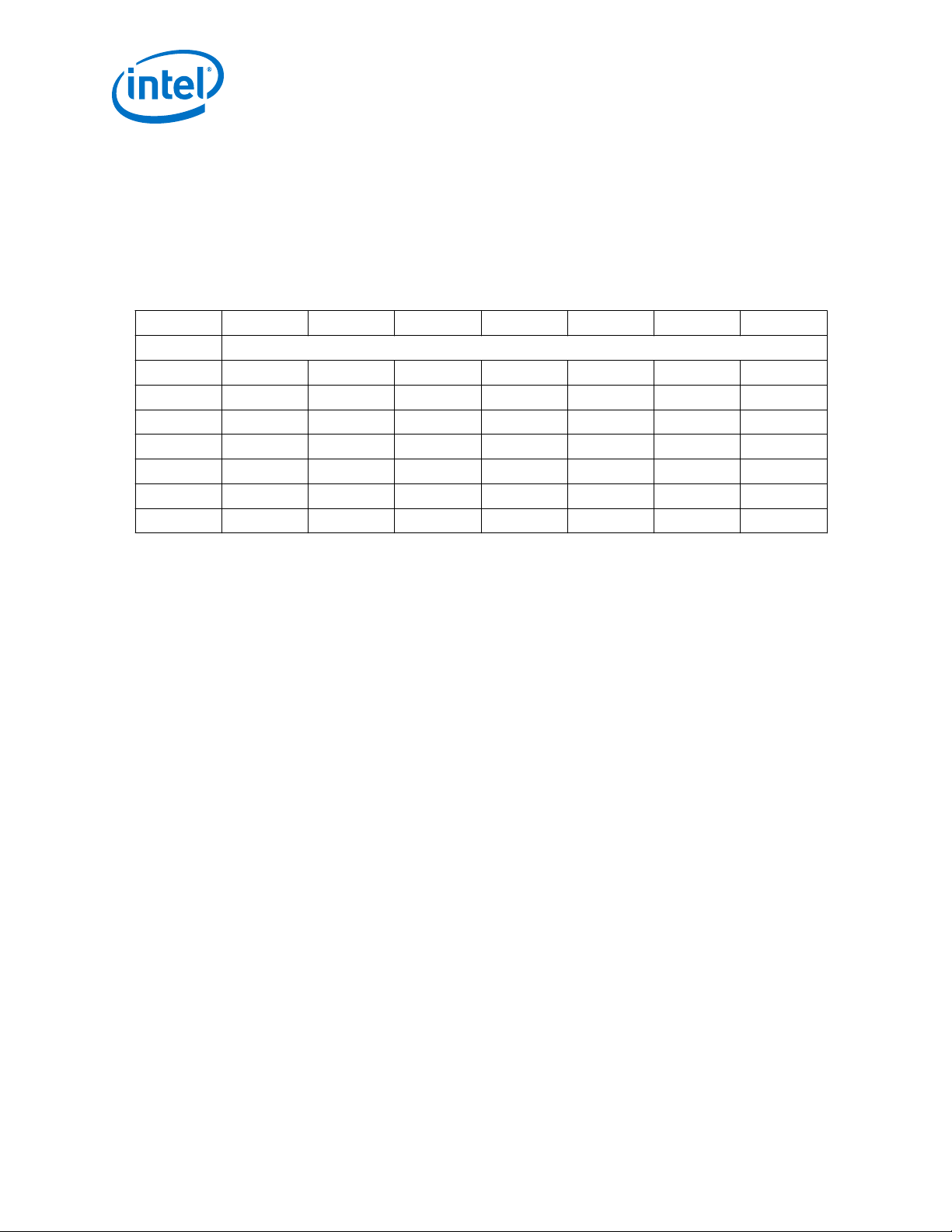
Table 1. Data Rates Supported by GX Transceiver Channel Type
Device Variant Standard Power Mode
Chip-to-Chip Backplane Chip-to-Chip
(3)
SX
(3)
GX
(4)
GT
(1)
To operate GX transceiver channels at designated data rates in standard and reduced power
1.0 Gbps to 17.4 Gbps 1.0 Gbps to 12.5 Gbps 1.0 Gbps to 11.3 Gbps
1.0 Gbps to 17.4 Gbps 1.0 Gbps to 12.5 Gbps 1.0 Gbps to 11.3 Gbps
1.0 Gbps to 17.4 Gbps 1.0 Gbps to 12.5 Gbps 1.0 Gbps to 11.3 Gbps
(1), (2)
Reduced Power Mode
modes, apply the corresponding core and periphery power supplies. Refer to the Arria 10
Device Datasheet for more details.
(2)
The minimum operational data rate is 1.0 Gbps for both the transmitter and receiver. For
transmitter data rates less than 1.0 Gbps, oversampling must be applied at the transmitter. For
receiver data rates less than 1.0 Gbps, oversampling must be applied at the receiver.
(3)
For SX and GX device variants, the maximum transceiver data rates are specified for the
fastest (–1) transceiver speed grade.
Intel Corporation. All rights reserved. Intel, the Intel logo, Altera, Arria, Cyclone, Enpirion, MAX, Nios, Quartus
and Stratix words and logos are trademarks of Intel Corporation or its subsidiaries in the U.S. and/or other
countries. Intel warrants performance of its FPGA and semiconductor products to current specifications in
accordance with Intel's standard warranty, but reserves the right to make changes to any products and services
at any time without notice. Intel assumes no responsibility or liability arising out of the application or use of any
information, product, or service described herein except as expressly agreed to in writing by Intel. Intel
customers are advised to obtain the latest version of device specifications before relying on any published
information and before placing orders for products or services.
*Other names and brands may be claimed as the property of others.
(1), (2)
ISO
9001:2008
Registered
Page 9
Core Logic Fabric
M20K Internal Memory Blocks
Transceiver Channels
Hard IP Per Transceiver: Standard PCS, PCIe Gen3 PCS, Enhanced PCS
PCI Express Gen3 Hard IP
PLLs
M20K Internal Memory Blocks
PCI Express Gen3 Hard IP
Variable Precision DSP Blocks
I/O PLLs
Hard Memory Controllers, General-Purpose I/O Cells, LVDS
M20K Internal Memory BlocksM20K Internal Memory Blocks
Variable Precision DSP Blocks
Core Logic Fabric
I/O PLLs
Hard Memory Controllers, General-Purpose I/O Cells, LVDS
M20K Internal Memory BlocksM20K Internal Memory Blocks
Variable Precision DSP Blocks
Transceiver Channels
PCI Express Gen3 Hard IP PCI Express Gen3 Hard IP
PLLs
Hard IP Per Transceiver: Standard PCS, PCIe Gen3 PCS, Enhanced PCS
1. Arria® 10 Transceiver PHY Overview
UG-01143 | 2018.06.15
Table 2. Data Rates Supported by GT Transceiver Channel Type
Device Variant
GT 1.0 Gbps to 25.8 Gbps 1.0 Gbps to 12.5 Gbps
(4)
Data Rates
Chip-to-Chip Backplane
(5), (2)
Note: The device data rates depend on the device speed grade. Refer to IntelArria 10 Device
Datasheet for details on available speed grades and supported data rates.
Related Information
• IntelArria 10 Device Datasheet
• IntelArria 10 Device Overview
1.1. Device Transceiver Layout
Figure 1. Arria 10 FPGA Architecture Block Diagram
The transceiver channels are placed on the left side periphery in most Arria 10 devices. For larger Arria 10
devices, additional transceiver channels are placed on the right side periphery.
(4)
For GT device variants, the maximum transceiver data rates are specified for (-1) transceiver
speed grade.
(5)
Because the GT transceiver channels are designed for peak performance, they do not have a
reduced power mode of operation.
Intel® Arria® 10 Transceiver PHY User Guide
9
Page 10

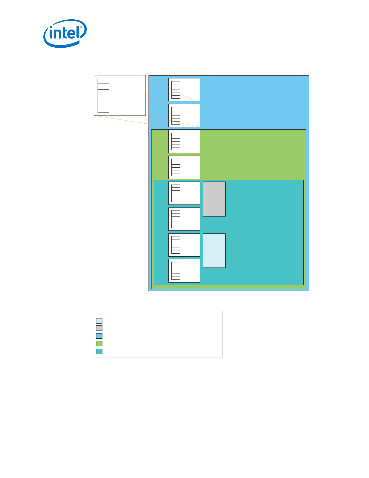
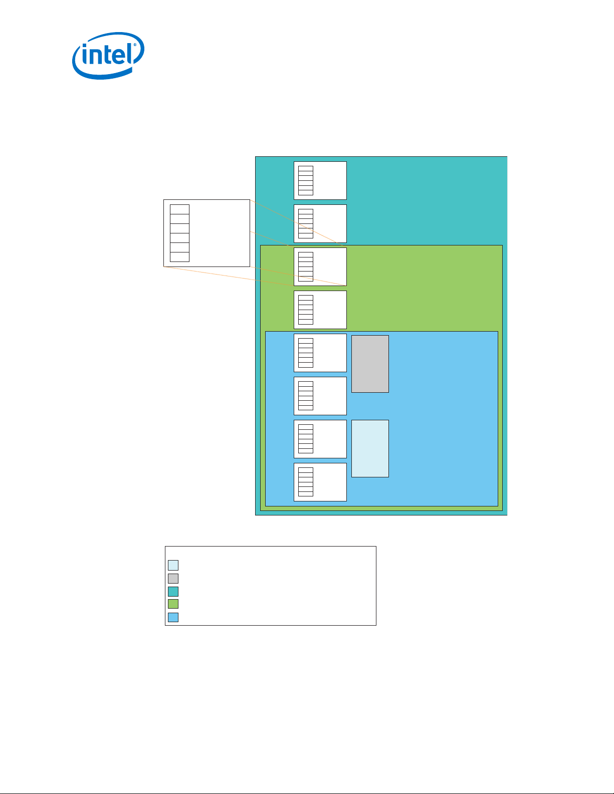
1.1.1. Arria 10 GX Device Transceiver Layout
The largest Arria 10 GX device includes 96 transceiver channels. A column array of
eight transceiver banks on the left and the right side periphery of the device is shown
in the following figure. Each transceiver bank has six transceiver channels. Some
devices have transceiver banks with only three channels. The transceiver banks with
only three channels are the uppermost transceiver banks. Arria 10 devices also include
PCI Express* Hard IP blocks.
The figures below illustrate different transceiver bank layouts for Arria 10 GX device
variants.
For more information about PCIe* Hard IP transceiver placements, refer to Related
Information at the end of this section.
1. Arria® 10 Transceiver PHY Overview
UG-01143 | 2018.06.15
Intel® Arria® 10 Transceiver PHY User Guide
10
Page 11

Transceiver
Bank
Transceiver
Bank
Transceiver
Bank
GXBL1J
Transceiver
Bank
GXBL1I
Transceiver
Bank
GXBL1H
Transceiver
Bank
Transceiver
Bank
GXBL1F
Transceiver
Bank
Transceiver
Bank
GXBL1D
Transceiver
Bank
Transceiver
Bank
Transceiver
Bank
Transceiver
Bank
Transceiver
Bank
GXBL1G
Transceiver
Bank
Transceiver
Bank
GXBL1E
Transceiver
Bank
Transceiver
Bank
GXBL1C
GXBR4J
Transceiver
Bank
GXBR4I
GXBR4H
Transceiver
Bank
GXBR4G
Transceiver
Bank
GXBR4F
Transceiver
Bank
GXBR4E
Transceiver
Bank
GXBR4D
Transceiver
Bank
GXBR4C
PCIe
Gen1 - Gen3
Hard IP
CH5
CH4
CH3
CH2
CH1
CH0
Transceiver
Bank
Notes:
(1) Nomenclature of left column bottom transceiver banks always ends with “C”.
(2) Nomenclature of right column bottom transceiver banks may end with “C”, “D”, or “E”.
(1) (2)
Legend:
PCIe Gen1 - Gen3 Hard IP blocks with Configuration via Protocol (CvP) capabilities.
PCIe Gen1 - Gen3 Hard IP blocks without Configuration via Protocol (CvP) capabilities.
GX 115 UF45
GX 090 UF45
PCIe
Gen1 - Gen3
Hard IP
(with CvP)
PCIe
Gen1 - Gen3
Hard IP
PCIe
Gen1 - Gen3
Hard IP
Arria 10 GX device with 96 transceiver channels and four PCIe Hard IP blocks.
1. Arria® 10 Transceiver PHY Overview
UG-01143 | 2018.06.15
Figure 2. Arria 10 GX Devices with 96 Transceiver Channels and Four PCIe Hard IP
Blocks
Intel® Arria® 10 Transceiver PHY User Guide
11
Page 12
Transceiver
Bank
Transceiver
Bank
Transceiver
Bank
Transceiver
Bank
Transceiver
Bank
Transceiver
Bank
Transceiver
Bank
Transceiver
Bank
Transceiver
Bank
Transceiver
Bank
Transceiver
Bank
Transceiver
Bank
Transceiver
Bank
Transceiver
Bank
Transceiver
Bank
Transceiver
Bank
Transceiver
Bank
Transceiver
Bank
CH5
CH4
CH3
CH2
CH1
CH0
Transceiver
Bank
GXBL1H
GXBL1G
GXBL1F
GXBL1E
GXBL1D
GXBL1C
GXBR4H
GXBR4G
GXBR4F
GXBR4E
GXBR4D
GXBR4C
(1) (2)
Notes:
(1) Nomenclature of left column bottom transceiver banks always ends with “C”.
(2) Nomenclature of right column bottom transceiver banks may end with “C”, “D”, or “E”.
GX 115 SF45
GX 090 SF45
GX 115 NF45
GX 090 NF45
PCIe
Gen1 - Gen3
Hard IP
PCIe
Gen1 - Gen3
Hard IP
PCIe
Gen1 - Gen3
Hard IP
(with CvP)
PCIe
Gen1 - Gen3
Hard IP
Legend:
PCIe Gen1 - Gen3 Hard IP blocks with Configuration via Protocol (CvP) capabilities.
PCIe Gen1 - Gen3 Hard IP blocks without Configuration via Protocol (CvP) capabilities.
Arria 10 GX device with 48 transceiver channels and four PCIe Hard IP blocks.
Arria 10 GX device with 72 transceiver channels and four PCIe Hard IP blocks.
1. Arria® 10 Transceiver PHY Overview
UG-01143 | 2018.06.15
Figure 3. Arria 10 GX Devices with 72 and 48 Transceiver Channels and Four PCIe Hard
IP Blocks.
Intel® Arria® 10 Transceiver PHY User Guide
12
Page 13
Transceiver
Bank
Transceiver
Bank
GXBL1H
Transceiver
Bank
GXBL1G
Transceiver
Bank
GXBL1F
Transceiver
Bank
GXBL1E
Transceiver
Bank
GXBL1D
Transceiver
Bank
GXBL1C
Transceiver
Bank
Transceiver
Bank
Transceiver
Bank
Transceiver
Bank
Transceiver
Bank
Transceiver
Bank
GXBR4J
Transceiver
Bank
GXBR4I
Transceiver
Bank
GXBR4H
Transceiver
Bank
GXBR4G
Transceiver
Bank
GXBR4F
Transceiver
Bank
GXBR4E
CH5
CH4
CH3
CH2
CH1
CH0
Transceiver
Bank
GX 115 RF40
GX 090 RF40
CH2
CH1
CH0
Transceiver
Bank
(1)
(2)
Notes:
(1) Nomenclature of left column bottom transceiver banks always ends with “C”.
(2) Nomenclature of right column bottom transceiver banks may end with “C”, “D”, or “E”.
PCIe
Gen1 - Gen3
Hard IP
PCIe
Gen1 - Gen3
Hard IP
(with CvP)
PCIe
Gen1 - Gen3
Hard IP
Legend:
PCIe Gen1 - Gen3 Hard IP blocks with Configuration via Protocol (CvP) capabilities.
PCIe Gen1 - Gen3 Hard IP blocks without Configuration via Protocol (CvP) capabilities.
Arria 10 GX device with 66 transceiver channels and three PCIe Hard IP blocks.
1. Arria® 10 Transceiver PHY Overview
UG-01143 | 2018.06.15
Figure 4. Arria 10 GX Devices with 66 Transceiver Channels and Three PCIe Hard IP
Blocks
Intel® Arria® 10 Transceiver PHY User Guide
13
Page 14
Transceiver
Bank
Transceiver
Bank
GXBL1I
Transceiver
Bank
GXBL1H
Transceiver
Bank
GXBL1G
Transceiver
Bank
GXBL1F
Transceiver
Bank
GXBL1E
Transceiver
Bank
GXBL1D
Transceiver
Bank
GXBL1C
Transceiver
Bank
Transceiver
Bank
Transceiver
Bank
Transceiver
Bank
Transceiver
Bank
Transceiver
Bank
Transceiver
Bank
Transceiver
Bank
GX 115 NF40
GX 090 NF40
GX 066 NF40
GX 057 NF40
GX 066 KF35
GX 057 KF35
GX 048 KF35
GX 115 HF34
GX 090 HF34
GX 066 HF34
GX 057 HF34
GX 048 HF34
GX 032 HF35
GX 032 HF34
GX 027 HF35
GX 027 HF34
CH5
CH4
CH3
CH2
CH1
CH0
Transceiver
Bank
GXBL1J
GXBL1C
GXBL1D
GXBL1E
GXBL1F
GXBL1G
GXBL1H
GXBL1I
GXBL1J
Note:
(1) These devices have transceivers only on the left hand side of the device.
GX 066 KF40
GX 057 KF40
PCIe
Gen1 - Gen3
Hard IP
PCIe
Gen1 - Gen3
Hard IP
(with CvP)
Legend:
PCIe Gen1 - Gen3 Hard IP blocks with Configuration via Protocol (CvP) capabilities.
PCIe Gen1 - Gen3 Hard IP blocks without Configuration via Protocol (CvP) capabilities.
Arria 10 GX device with 48 transceiver channels and two PCIe Hard IP blocks.
Arria 10 GX device with 36 transceiver channels and two PCIe Hard IP blocks.
Arria 10 GX device with 24 transceiver channels and two PCIe Hard IP blocks.
1. Arria® 10 Transceiver PHY Overview
UG-01143 | 2018.06.15
Figure 5. Arria 10 GX Devices with 48, 36, and 24 Transceiver Channels and Two PCIe
Hard IP Blocks
Intel® Arria® 10 Transceiver PHY User Guide
14
Page 15
Transceiver
Bank
GXBL1D
Transceiver
Bank
GXBL1C
Transceiver
Bank
Transceiver
Bank
GX 048 EF29
GX 032 EF29
GX 027 EF29
GX 032 EF27
GX 027 EF27
GX 022 EF29
GX 022 EF27
GX 016 EF29
GX 016 EF27
CH5
CH4
CH3
CH2
CH1
CH0
Transceiver
Bank
Note:
(1) These devices have transceivers only on the left hand side of the device.
Legend:
PCIe Gen1 - Gen3 Hard IP blocks with Configuration via Protocol (CvP) capabilities.
Arria 10 GX device with 12 transceiver channels and one PCIe Hard IP block.
PCIe
Gen1 - Gen3
Hard IP
(with CvP)
Transceiver
Bank
GXBL1C Transceiver
Bank
PCIe Hard IP
GX 022 CU19
GX 016 CU19
CH5
CH4
CH3
CH2
CH1
CH0
Transceiver
Bank
GXBL1C
Note:
(2) These devices have transceivers only on the left hand side of the device.
Legend:
PCIe Gen1 - Gen3 Hard IP block with Configuration via Protocol (CvP) capabilities.
Arria 10 GX device with six transceiver channels and one PCIe Hard IP block.
(1)
(1) Only CH5 and CH4 support PCIe Hard IP block with CvP capabilities.
®
1. Arria
UG-01143 | 2018.06.15
10 Transceiver PHY Overview
Figure 6. Arria 10 GX Devices with 12 Transceiver Channels and One PCIe Hard IP
Block
Figure 7. Arria 10 GX Devices with 6 Transceiver Channels and One PCIe Hard IP Block
Related Information
• IntelArria 10 Avalon-ST Interface for PCIe Solutions User Guide
• IntelArria 10 Avalon-MM Interface for PCIe Solutions User Guide
• IntelArria 10 Avalon-MM DMA Interface for PCIe Solutions User Guide
• IntelArria 10 Avalon-ST Interface with SR-IOV PCIe Solutions User Guide
1.1.2. Arria 10 GT Device Transceiver Layout
The Arria 10 GT device has 72 transceiver channels and four PCI Express Hard IP
blocks. A total of 6 GT transceiver channels that can support data rates up to 25.8
Gbps.
In the GT device, transceiver banks GXBL1E, GXBL1G, and GXBL1H each contain two
GT transceiver channels. Transceiver banks GXBL1E and GXBL1H channels 3 and 4 can
be used as GT or GX transceiver channel. Transceiver bank GXBL1G channels 0 and 1
can be used as GT or GX transceiver channels. When none of the GT capable
transceiver channels are used as GT transceiver channels, the entire transceiver
Intel® Arria® 10 Transceiver PHY User Guide
15
Page 16
Transceiver
Bank
Transceiver
Bank
Transceiver
Bank
Transceiver
Bank
Transceiver
Bank
Transceiver
Bank
Transceiver
Bank
Transceiver
Bank
Transceiver
Bank
Transceiver
Bank
Transceiver
Bank (3)
Transceiver
Bank
Transceiver
Bank
Transceiver
Bank
Transceiver
Bank
Transceiver
Bank
Transceiver
Bank
Transceiver
Bank
Transceiver
Bank
GT 115 SF45
GT 090 SF45
GT Channels
Capable of Short
Reach 25.8 Gbps
GXBL1C
GXBL1D
GXBL1E
GXBL1F
GXBL1G
GXBL1H
GXBR4C
GXBR4D
GXBR4E
GXBR4F
GXBR4G
GXBR4H
Notes:
(1) Nomenclature of left column bottom transceiver banks always end with “C”.
(2) Nomenclature of right column bottom transceiver banks may end with “C”, “D”, or “E”.
(3) If a GT channel is used in transceiver bank GXBL1E, the PCIe Hard IP adjacent to GXBL1F and GXBL1E cannot be used.
(1) (2)
GX or Restricted
GT or GX
GT or GX
GX or Restricted
CH5
CH4
CH3
CH2
CH1
CH0
PCIe
Gen1 - Gen3
Hard IP
PCIe
Gen1 - Gen3
Hard IP
PCIe
Gen1 - Gen3
Hard IP
PCIe
Gen1 - Gen3
(with CvP)
Hard IP
Legend:
GX transceiver channels (channel 2 and 5) with usage restrictions.
GT transceiver channels (channel 0, 1, 3, and 4).
PCIe Gen1 - Gen3 Hard IP blocks with Configuration via Protocol (CvP) capabilities.
PCIe Gen1 - Gen3 Hard IP blocks without Configuration via Protocol (CvP) capabilities.
GX transceiver channels without usage restrictions.
GX or Restricted
GX or Restricted
GT or GX
GT or GX
CH5
CH4
CH3
CH2
CH1
CH0
GX or Restricted
GX or Restricted
GX or Restricted
GX or Restricted
®
1. Arria
10 Transceiver PHY Overview
UG-01143 | 2018.06.15
channels in the bank can be reconfigured as GX transceiver channels. However, when
any of the GT capable transceiver channels in transceiver banks GXBL1E, GXBL1G,
and GXBL1H is enabled as a GT transceiver channel, the remaining channels in the
transceiver bank cannot be used with the exception of the other GT capable channel in
the transceiver bank.
If you're using GT transceivers in bank GXBL1E, then the adjacent PCIe Hard IP block
cannot be used.
Figure 8. Arria 10 GT Device with 72 Transceiver Channels and Four PCIe Hard IP
Blocks
The GT device has 72 transceiver channels, which include 6 GT transceiver channels
supporting data rates greater than 17.4 Gbps. If all six GT transceiver channels are
used in GT mode, there are 54 GX transceiver channels that can drive chip to chip
data rates up to 17.4 Gbps and backplanes at data rates up to 12.5 Gbps and 12 GX
In the GT device, the GX transceiver channels on the entire right side can be used in
standard or reduced power mode. In GT devices where none of the GT channels are
used to operate in GT data rates above 17.4 Gbps, the transceiver channels on either
channels that are unusable.
the entire right side or entire left side can be used as GX channels in standard or
reduced power mode.
Related Information
• IntelArria 10 Avalon-ST Interface for PCIe Solutions User Guide
• IntelArria 10 Avalon-MM Interface for PCIe Solutions User Guide
• IntelArria 10 Avalon-MM DMA Interface for PCIe Solutions User Guide
Intel® Arria® 10 Transceiver PHY User Guide
16
Page 17
®
1. Arria
UG-01143 | 2018.06.15
10 Transceiver PHY Overview
• IntelArria 10 Avalon-ST Interface with SR-IOV PCIe Solutions User Guide
1.1.3. Arria 10 GX and GT Device Package Details
The following tables list package sizes, available transceiver channels, and PCI Express
Hard IP blocks for Arria 10 GX and GT devices.
Table 3. Package Details for GX Devices with Transceivers and Hard IP Blocks Located
on the Left Side Periphery of the Device
• Package U19: 19mm x 19mm package; 484 pins.
• Package F27: 27mm x 27mm package; 672 pins.
• Package F29: 29mm x 29mm package; 780 pins.
• Packages F34 and F35: 35 mm x 35 mm package size; 1152 pins.
• Package F40: 40 mm x 40 mm package size; 1517 pins. K = 36 transceiver channels, N = 48 transceiver
channels.
Device U19 F27 F29 F34 F35 K F40 N F40
Transceiver Count, PCIe Hard IP Block Count
GX 016 6, 1 12, 1 12, 1
GX 022 6, 1 12, 1 12, 1
GX 027 12, 1 12, 1 24, 2 24, 2
GX 032 12, 1 12, 1 24, 2 24, 2
GX 048 12, 1 24, 2 36, 2
GX 057 24, 2 36, 2 36, 2 48, 2
GX 066 24, 2 36, 2 36, 2 48, 2
GX 090 24, 2 48, 2
GX 115 24, 2 48, 2
Table 4. Package Details for GX and GT Devices with Transceivers and Hard IP Blocks
Located on the Left and Right Side Periphery of the Device
• Package F40: 40 mm x 40 mm package size; 1517 pins. R = 66 transceiver channels.
• Package F45: 45mm x 45mm package size; 1932 pins. N = 48 transceiver channels, S = 72 transceiver
channels, U = 96 transceiver channels.
• If you're using GT transceivers in bank GXBL1E, the nth adjacent PCIe Hard IP block cannot be used.
Device
GX 090 66, 3 48, 4 72, 4 96, 4
GX 115 66, 3 48, 4 72, 4 96, 4
GT 090 72, 4
GT 115 72, 4
R F40 N F45 S F45 U F45
Transceiver Count, PCIe Hard IP Block Count
1.1.4. Arria 10 SX Device Transceiver Layout
The largest SX device includes 48 transceiver channels. All SX devices include GX
transceiver channel type. The transceiver banks in SX devices are located on the left
side periphery of the device.
Intel® Arria® 10 Transceiver PHY User Guide
17
Page 18
Transceiver
Bank
Transceiver
Bank
Transceiver
Bank
Transceiver
Bank
Transceiver
Bank
Transceiver
Bank
Transceiver
Bank
Transceiver
Bank
Transceiver
Bank
Transceiver
Bank
Transceiver
Bank
Transceiver
Bank
Transceiver
Bank
Transceiver
Bank
Transceiver
Bank
Transceiver
Bank
CH5
CH4
CH3
CH2
CH1
CH0
Transceiver
Bank
SX 066 NF40
SX 057 NF40
SX 066 KF35
SX 057 KF35
SX 048 KF35
SX 066 HF34
SX 057 HF34
SX 048 HF34
SX 032 HF35
SX 032 HF34
SX 027 HF35
SX 027 HF34
GXBL1C
GXBL1D
GXBL1E
GXBL1F
GXBL1G
GXBL1H
GXBL1I
GXBL1J
Note:
(1) These devices have transceivers only on the left hand side of the device.
Legend:
PCIe Gen1- Gen3 Hard IP blocks with Configuration via Protocol (CvP) capabilities.
PCIe Gen1 - Gen3 Hard IP blocks without Configuration via Protocol (CvP) capabilities.
PCIe
Gen1 - Gen3
Hard IP
PCIe
Gen1 - Gen3
(with CvP)
Hard IP
Arria 10 SX device with 24 transceiver channels and two PCIe Hard IP blocks.
Arria 10 SX device with 36 transceiver channels and two PCIe Hard IP blocks.
Arria 10 SX device with 48 transceiver channels and two PCIe Hard IP blocks.
SX 066 KF40
SX 057 KF40
1. Arria® 10 Transceiver PHY Overview
UG-01143 | 2018.06.15
For more information about PCIe Hard IP transceiver placements, refer to Related
Information at the end of this section.
Figure 9. Arria 10 SX Device with 48, 36, and 24 Transceiver Channels and Two Hard IP
Blocks
Intel® Arria® 10 Transceiver PHY User Guide
18
Page 19
Transceiver
Bank
Transceiver
Bank
Transceiver
Bank
Transceiver
Bank
PCIe
Gen1 - Gen3
Hard IP
(with CvP)
CH5
CH4
CH3
CH2
CH1
CH0
Transceiver
Bank
SX 022 EF29
SX 022 EF27
SX 016 EF29
SX 016 EF27
SX 048 EF29
SX 032 EF29
SX 032 EF27
SX 027 EF29
SX 027 EF27
GXBL1D
GXBL1C
GXBL1D
GXBL1C
Note:
(1) These devices have transceivers only on the left hand side of the device.
Legend:
PCIe Gen1 - Gen3 Hard IP blocks with Configuration via Protocol (CvP) capabilities.
Arria 10 SX device with 12 transceiver channels and one Hard IP block.
Transceiver
Bank
GXBL1C Transceiver
Bank
PCIe Hard IP
SX 022 CU19
SX 016 CU19
CH5
CH4
CH3
CH2
CH1
CH0
Transceiver
Bank
Legend:
PCIe Gen1 - Gen3 Hard IP block with Configuration via Protocol (CvP) capabilities.
Arria 10 SX device with six transceiver channels and one PCIe Hard IP block.
Note:
(2) These devices have transceivers only on the left hand side of the device.
(1) Only CH5 and CH4 support PCIe Hard IP block with Configuration via Protocol (CvP) capabilities.
(1)
®
1. Arria
UG-01143 | 2018.06.15
10 Transceiver PHY Overview
Figure 10. Arria 10 SX Device with 12 Transceiver Channels and One Hard IP Block
Figure 11. Arria 10 SX Device with Six Transceiver Channels and One Hard IP Block
Related Information
• IntelArria 10 Avalon-ST Interface for PCIe Solutions User Guide
• IntelArria 10 Avalon-MM Interface for PCIe Solutions User Guide
1.1.5. Arria 10 SX Device Package Details
• IntelArria 10 Avalon-MM DMA Interface for PCIe Solutions User Guide
• IntelArria 10 Avalon-ST Interface with SR-IOV PCIe Solutions User Guide
The following tables list package sizes, available transceiver channels, and PCI Express
Hard IP blocks for Arria 10 SX devices.
Intel® Arria® 10 Transceiver PHY User Guide
19
Page 20
®
1. Arria
10 Transceiver PHY Overview
UG-01143 | 2018.06.15
Table 5. Package Details for SX Devices with Transceivers and Hard IP Blocks Located
on the Left Side Periphery of the Device
• Package U19: 19mm x 19mm package; 484 pins.
• Package F27: 27mm x 27mm package; 672 pins.
• Package F29: 29mm x 29mm package; 780 pins.
• Packages F34 and F35: 35 mm x 35 mm package size; 1152 pins.
• Package F40: 40 mm x 40 mm package size; 1517 pins. K = 36 transceiver channels, N = 48 transceiver
channels.
Device U19 F27 F29 F34 F35 K F40 N F40
Transceiver Count, PCIe Hard IP Block Count
SX 016 6, 1 12, 1 12, 1
SX 022 6, 1 12, 1 12, 1
SX 027 12, 1 12, 1 24, 2 24, 2
SX 032 12, 1 12, 1 24, 2 24, 2
SX 048 12, 1 24, 2 36, 2
SX 057 24, 2 36, 2 36, 2 48, 2
SX 066 24, 2 36, 2 36, 2 48, 2
1.2. Transceiver PHY Architecture Overview
A link is defined as a single entity communication port. A link can have one or more
transceiver channels. A transceiver channel is synonymous with a transceiver lane.
For example, a 10GBASE-R link has one transceiver channel or lane with a data rate of
10.3125 Gbps. A 40GBASE-R link has four transceiver channels. Each transceiver
channel operates at a lane data rate of 10.3125 Gbps. Four transceiver channels give
a total collective link bandwidth of 41.25 Gbps (40 Gbps before and after 64B/66B
Physical Coding Sublayer (PCS) encoding and decoding).
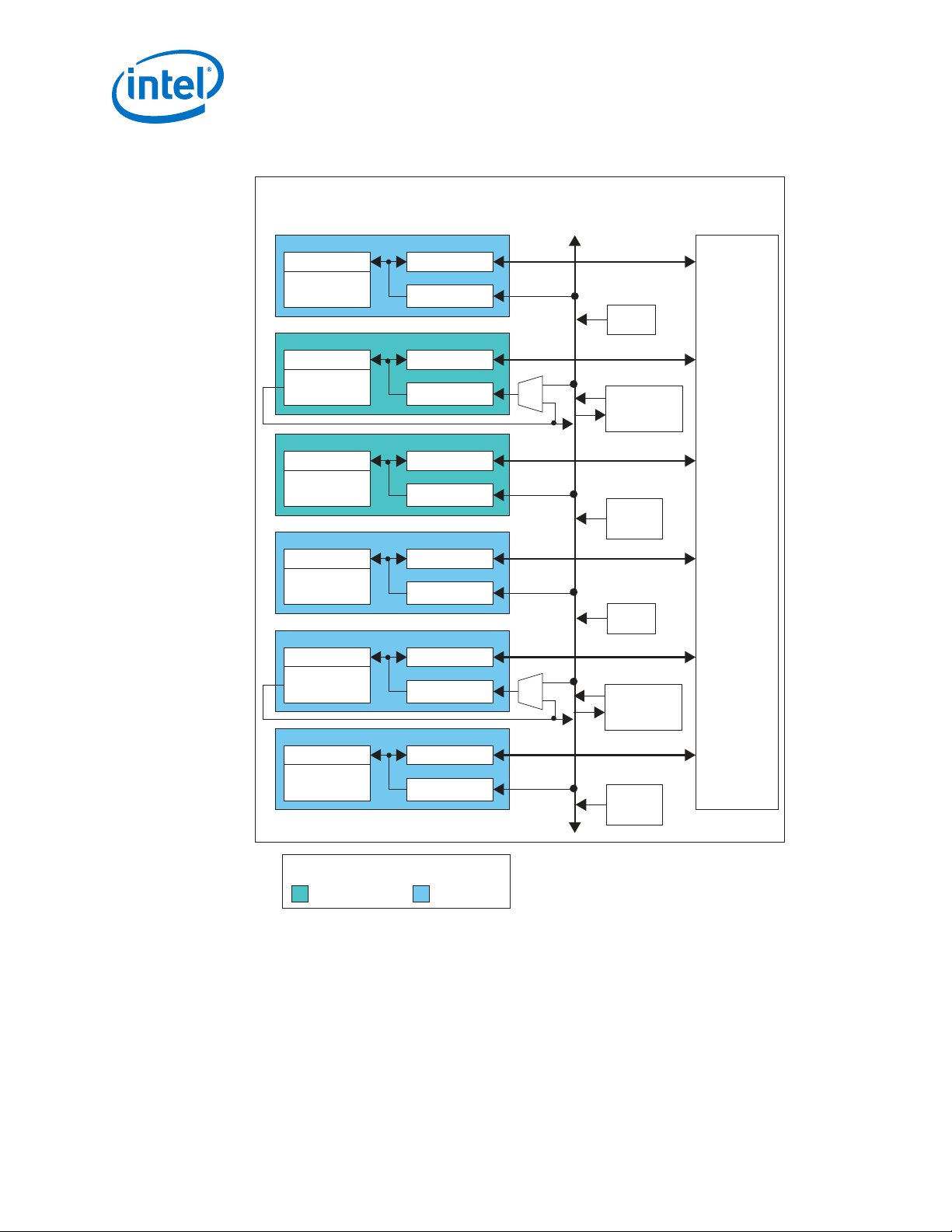
1.2.1. Transceiver Bank Architecture
The transceiver bank is the fundamental unit that contains all the functional blocks
related to the device's high speed serial transceivers.
Each transceiver bank includes six transceiver channels in all devices except for the
devices with 66 transceiver channels. Devices with 66 transceiver channels have both
six channel and three channel transceiver banks. The uppermost transceiver bank on
the left and the right side of these devices is a three channel transceiver bank. All
other devices contain only six channel transceiver banks.
The figures below show the transceiver bank architecture with the phase locked loop
(PLL) and clock generation block (CGB) resources available in each bank.
Intel® Arria® 10 Transceiver PHY User Guide
20
Page 21
PMA
Channel PLL
(CDR Only)
PCS
Local CGB2
CH2
PMA
Channel PLL
(CMU/CDR)
PCS
Local CGB1
CH1
PMA
Channel PLL
(CDR Only)
PCS
Local CGB0
CH0
FPGA Core
Fabric
Three-Channel GX Transceiver Bank
Master
CGB0
fPLL0
ATX
PLL0
Clock
Distribution
Network
1. Arria® 10 Transceiver PHY Overview
UG-01143 | 2018.06.15
Figure 12. Three-Channel GX Transceiver Bank Architecture
Note: This figure is a high level overview of the transceiver bank architecture. For details
about the available clock networks refer to the PLLs and Clock Networks chapter.
Intel® Arria® 10 Transceiver PHY User Guide
21
Page 22

Figure 13. Six-Channel GX Transceiver Bank Architecture
PMA
Channel PLL
(CDR Only)
PCS
Local CGB5
CH5
PMA
Channel PLL
(CMU/CDR)
PCS
Local CGB4
CH4
PMA
Channel PLL
(CDR Only)
PCS
Local CGB3
CH3
PMA
Channel PLL
(CDR Only)
PCS
Local CGB2
CH2
PMA
Channel PLL
(CMU/CDR)
PCS
Local CGB1
CH1
PMA
Channel PLL
(CDR Only)
PCS
Local CGB0
CH0
FPGA Core
Fabric
Clock
Distribution
Network
Six-Channel GX Transceiver Bank
fPLL1
Master
CGB1
Master
CGB0
ATX
PLL0
ATX
PLL1
fPLL0
1. Arria® 10 Transceiver PHY Overview
UG-01143 | 2018.06.15
Note: This figure is a high level overview of the transceiver bank architecture. For details
Intel® Arria® 10 Transceiver PHY User Guide
22
about the available clock networks refer to the PLLs and Clock Networks chapter.
Page 23

CH1
PMA
Channel PLL
(CDR Only)
PCS
Local CGB5
CH5
PMA
Channel PLL
(CMU/CDR)
PCS
Local CGB4
CH4
PMA
Channel PLL
(CDR Only)
PCS
Local CGB3
CH3
PMA
Channel PLL
(CDR Only)
PCS
Local CGB2
CH2
PMA
Channel PLL
(CMU/CDR)
PCS
Local CGB1
PMA
Channel PLL
(CDR Only)
PCS
Local CGB0
CH0
FPGA Core
Fabric
Clock
Distribution
Network
Six-Channel GT Transceiver Bank GXBL1G
fPLL1
Master
CGB1
Master
CGB0
ATX
PLL1
ATX
PLL0
fPLL0
GX Channel
GT/GX Channel
Legend
1. Arria® 10 Transceiver PHY Overview
UG-01143 | 2018.06.15
Figure 14. GT Transceiver Bank Architecture
In the GT device, the transceiver banks GXBL1E, GXBL1G, and GXBL1H include GT channels.
Note: This figure is a high level overview of the transceiver bank architecture. For details
about the available clock networks refer to the PLLs and Clock Networks chapter.
Intel® Arria® 10 Transceiver PHY User Guide
23
Page 24
CH1
PMA
Channel PLL
(CDR Only)
PCS
Local CGB5
CH5
PMA
Channel PLL
(CMU/CDR)
PCS
Local CGB4
CH4
PMA
Channel PLL
(CDR Only)
PCS
Local CGB3
CH3
PMA
Channel PLL
(CDR Only)
PCS
Local CGB2
CH2
PMA
Channel PLL
(CMU/CDR)
PCS
Local CGB1
PMA
Channel PLL
(CDR Only)
PCS
Local CGB0
CH0
FPGA Core
Fabric
Clock
Distribution
Network
Six-Channel GT
Transceiver Banks GXBL1E and GXBL1H
fPLL1
Master
CGB1
Master
CGB0
ATX
PLL1
ATX
PLL0
fPLL0
GX Channel
GT/GX Channel
Legend
®
1. Arria
Figure 15. GT Transceiver Bank Architecture for Banks GXBL1E and GXBL1H
10 Transceiver PHY Overview
UG-01143 | 2018.06.15
Note: This figure is a high level overview of the transceiver bank architecture. For details
Intel® Arria® 10 Transceiver PHY User Guide
24
about the available clock networks refer to the PLLs and Clock Networks chapter.
The transceiver channels perform all the required PHY layer functions between the
FPGA fabric and the physical medium. The high speed clock required by the
transceiver channels is generated by the transceiver PLLs. The master and local clock
generation blocks (CGBs) provide the necessary high speed serial and low speed
parallel clocks to drive the non-bonded and bonded channels in the transceiver bank.
Page 25

Standard PCS
PCIe Gen3 PCS
Enhanced PCSKR FEC
PCS Direct
Hard IP
(Optional)
Soft PIPE
(Optional)
FPGA Fabric
Transmitter PCS
Transmitter PMA
Serializer
Standard PCS
PCIe Gen3 PCS
Enhanced PCSKR FEC
PCS Direct
Receiver PCS
Receiver PMA
DeserializerCDR
Notes:
(1) The FPGA Fabric - PCS and PCS-PMA interface widths are configurable.
(1)
(1)
(1)
(1)
®
1. Arria
UG-01143 | 2018.06.15
10 Transceiver PHY Overview
Related Information
• PLLs and Clock Networks on page 347
• Transceiver Basics
Online training course for transceivers.
1.2.2. PHY Layer Transceiver Components
Transceivers in Arria 10 devices support both Physical Medium Attachment (PMA) and
Physical Coding Sublayer (PCS) functions at the physical (PHY) layer.
A PMA is the transceiver's electrical interface to the physical medium. The transceiver
PMA consists of standard blocks such as:
• serializer/deserializer (SERDES)
• clock and data recovery PLL
• analog front end transmit drivers
• analog front end receive buffers
The PCS can be bypassed with a PCS Direct configuration. Both the PMA and PCS
blocks are fed by multiple clock networks driven by high performance PLLs. In PCS
Direct configuration, the data flow is through the PCS block, but all the internal PCS
blocks are bypassed. In this mode, the PCS functionality is implemented in the FPGA
fabric.
1.2.2.1. The GX Transceiver Channel
Figure 16. GX Transceiver Channel in Full Duplex Mode.
Arria 10 GX transceiver channels have three types of PCS blocks that together support
continuous data rates between 1.0 Gbps and 17.4 Gbps.
Intel® Arria® 10 Transceiver PHY User Guide
25
Page 26

1. Arria® 10 Transceiver PHY Overview
UG-01143 | 2018.06.15
Table 6. PCS Types Supported by GX Transceiver Channels
PCS Type Data Rate
Standard PCS 1.0 Gbps to 10.81344 Gbps
Enhanced PCS 1.0 Gbps
PCIe Gen3 PCS 8 Gbps
(6)
to 17.4 Gbps
Note: 1. The GX channel can also operate in PCS Direct configuration for data rates from
1.0 Gbps to 17.4 Gbps. To operate GX transceiver channels in PCS Direct
designated data rates, refer to the IntelArria 10 Device Datasheet for more details
on power supply, speed grade, and transceiver configurations requirement.
2. The minimum operational data rate is 1.0 Gbps for both the transmitter and
receiver. For transmitter data rates less than 1.0 Gbps, oversampling must be
applied at the transmitter. For receiver data rates less than 1.0 Gbps,
oversampling must be applied at the receiver.
3. To operate GX transceiver channels with the PCS at designated data rates, refer to
the IntelArria 10 Device Datasheet for more details on power supply, speed grade,
and transceiver configurations requirement.
Related Information
IntelArria 10 Device Datasheet
1.2.2.2. The GT Transceiver Channel
The GT transceiver channels are used for supporting data rates from 17.4 Gbps to
25.8 Gbps. The PCS Direct datapath that bypasses all PCS blocks is the primary
configuration used to support GT data rates from 17.4 Gbps to 25.8 Gbps.
Alternatively, the Enhanced PCS in Basic low latency configuration can also be used to
support GT data rates from 17.4 Gbps to 25.8 Gbps. The GT transceiver channels can
also be configured as GX transceiver channels. When they are configured as GX
transceiver channels, the Standard PCS, Enhanced PCS, and PCIe Gen3 PCS are
available and they support data rates from 1.0 Gbps to 17.4 Gbps.
(6)
Applies when operating in reduced power modes. For standard power modes, the Enhanced
PCS minimum data rate is 1600 Mbps.
Intel® Arria® 10 Transceiver PHY User Guide
26
Page 27
Notes:
(3) The Standard PCS and PCIe Gen3 PCS blocks are available when the GT channel is configured as a GX transceiver channel.
(1) The Enhanced PCS must be configured in Basic low latency mode to support data rate range from 17.4 Gbps to 25.8 Gbps.
(2) The FPGA Fabric - PCS and PCS-PMA interface widths are configurable.
Standard PCS
PCIe Gen3 PCS
Enhanced PCSKR FEC
PCS Direct
FPGA Fabric
Transmitter PCS
Transmitter PMA
Serializer
Standard PCS
PCIe Gen3 PCS
Enhanced PCSKR FEC
PCS Direct
Receiver PCS
Receiver PMA
DeserializerCDR
(1)
(1)
(2)
(2)
(2)
(2)
(3)
(3)
(3)
(3)
1. Arria® 10 Transceiver PHY Overview
UG-01143 | 2018.06.15
Figure 17. GT Transceiver Channel in Full Duplex Mode Operating Between 17.4 Gbps
and 25.8 Gbps
Table 7. PCS Types and Data Rates Supported by GT Channel Configurations
GT Channel Configuration PCS Type Data Rates Supported
GT Standard PCS Not available for GT configuration
Enhanced PCS 17.4 Gbps to 25.8 Gbps
PCIe Gen3 PCS Not available for GT configuration
GX Standard PCS 1.0 Gbps to 12 Gbps
Enhanced PCS 1.0 Gbps
PCIe Gen3 PCS 8 Gbps
Note: 1. The GT channels can also operate in PCS Direct configuration for data rates from
1.0 Gbps to 25.8 Gbps. The PCS Direct datapath that bypasses all PCS blocks is
the primary configuration used to support GT data rates from 17.4 Gbps to 25.8
Gbps. To operate GX and GT transceiver channels in PCS Direct designated data
rates, refer to the IntelArria 10 Device Datasheet for more details on power
supply, speed grade, and transceiver configurations requirement.
2. The minimum operational data rate is 1.0 Gbps for both the transmitter and
receiver. For transmitter data rates less than 1.0 Gbps, oversampling must be
applied at the transmitter. For receiver data rates less than 1.0 Gbps,
oversampling must be applied at the receiver.
3. To operate GX and GT transceiver channels with the PCS at designated data rates,
(7)
The Enhanced PCS must be configured in Basic low latency mode to support data rate range
refer to the IntelArria 10 Device Datasheet for more details on power supply,
speed grade, and transceiver configurations requirement.
from 17.4 Gbps to 25.8 Gbps.
(8)
Applies when operating in reduced power modes. For standard power modes, the Enhanced
PCS minimum data rate is 1600 Mbps.
(7)
(8)
to 17.4 Gbps
Intel® Arria® 10 Transceiver PHY User Guide
27
Page 28

Related Information
IntelArria 10 Device Datasheet
1.2.3. Transceiver Phase-Locked Loops
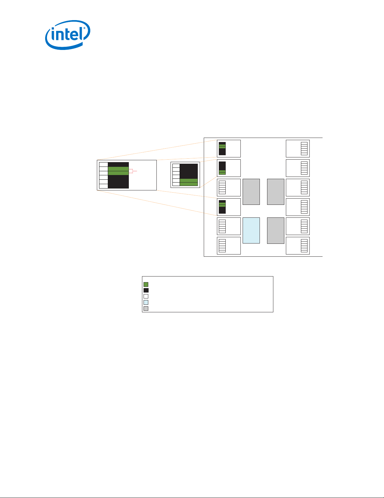
Each transceiver channel in Arria 10 devices has direct access to three types of high
performance PLLs:
• Advanced Transmit (ATX) PLL
• Fractional PLL (fPLL)
• Channel PLL / Clock Multiplier Unit (CMU) PLL.
These transceiver PLLs along with the Master or Local Clock Generation Blocks (CGB)
drive the transceiver channels.
Related Information
PLLs on page 349
For more information on transceiver PLLs in Arria 10 devices.
1.2.3.1. Advanced Transmit (ATX) PLL
1. Arria
®
10 Transceiver PHY Overview
UG-01143 | 2018.06.15
An advanced transmit (ATX ) PLL is a high performance PLL. It supports both integer
frequency synthesis and coarse resolution fractional frequency synthesis. The ATX PLL
is the transceiver channel’s primary transmit PLL. It can operate over the full range of
supported data rates required for high data rate applications.
Related Information
• ATX PLL on page 350
For more information on ATX PLL.
• ATX PLL IP Core on page 354
For details on implementing the ATX PLL IP.
1.2.3.2. Fractional PLL (fPLL)
A fractional PLL (fPLL) is an alternate transmit PLL used for generating lower clock
frequencies for 12.5 Gbps and lower data rate applications. fPLLs support both integer
frequency synthesis and fine resolution fractional frequency synthesis. Unlike the ATX
PLL, the fPLL can also be used to synthesize frequencies that can drive the core
through the FPGA fabric clock networks.
Related Information
• fPLL on page 359
For more information on fPLL.
• fPLL IP Core on page 362
For details on implementing the fPLL IP.
1.2.3.3. Channel PLL (CMU/CDR PLL)
A channel PLL resides locally within each transceiver channel. Its primary function is
clock and data recovery in the transceiver channel when the PLL is used in clock data
recovery (CDR) mode. The channel PLLs of channel 1 and 4 can be used as transmit
Intel® Arria® 10 Transceiver PHY User Guide
28
Page 29

®
1. Arria
UG-01143 | 2018.06.15
10 Transceiver PHY Overview
PLLs when configured in clock multiplier unit (CMU) mode. The channel PLLs of
channel 0, 2, 3, and 5 cannot be configured in CMU mode and therefore cannot be
used as transmit PLLs.
Related Information
• CMU PLL on page 368
For more information on CMU PLL.
• CMU PLL IP Core on page 370
For information on implementing CMU PLL IP.
1.2.4. Clock Generation Block (CGB)
In Arria 10 devices, there are two types of clock generation blocks (CGBs):
• Master CGB
• Local CGB
Transceiver banks with six transceiver channels have two master CGBs. Master CGB1
is located at the top of the transceiver bank and master CGB0 is located at the bottom
of the transceiver bank. Transceiver banks with three channels have only one master
CGB. The master CGB divides and distributes bonded clocks to a bonded channel
group. It also distributes non-bonded clocks to non-bonded channels across the x6/xN
clock network.
Each transceiver channel has a local CGB. The local CGB is used for dividing and
distributing non-bonded clocks to its own PCS and PMA blocks.
Related Information
Clock Generation Block on page 383
For more information on clock generation block.
1.3. Calibration
Arria 10 FPGAs contain a dedicated calibration engine to compensate for process
variations. The calibration engine calibrates the analog portion of the transceiver to
allow both the transmitter and receiver to operate at optimum performance.
The CLKUSR pin clocks the calibration engine. All transceiver reference clocks and the
CLKUSR clock must be free running and stable at the start of FPGA configuration to
successfully complete the calibration process and for optimal transceiver performance.
Note:
For more information about CLKUSR electrical characteristics, refer to IntelArria 10
Device Datasheet. The CLKUSR can also be used as an FPGA configuration clock. For
information about configuration requirements for the CLKUSR pin, refer to the
Configuration, Design Security, and Remote System Upgrades in Arria 10 Devices
chapter in the Arria 10 Core Fabric and General-Purpose I/O Handbook. For more
information about calibration, refer to the Calibration chapter. For more information
about CLKUSR pin requirements, refer to the IntelArria 10 GX, GT, and SX Device
Family Pin Connection Guidelines.
Related Information
• IntelArria 10 Device Datasheet
Intel® Arria® 10 Transceiver PHY User Guide
29
Page 30

1. Arria® 10 Transceiver PHY Overview
UG-01143 | 2018.06.15
• Configuration, Design Security, and Remote System Upgrades in Arria 10 Devices
• IntelArria 10 GX, GT, and SX Device Family Pin Connection Guidelines
1.4. Intel Arria 10 Transceiver PHY Overview Revision History
Document
Version
2018.06.15 Made the following changes:
• Changed the data rate range for the Standard PCS in the "PCS types Supported by GX Transceiver
Channels" table.
2016.05.02 Made the following changes:
• Maximum backplane rate updated from 16.0 Gbps to 12.5 Gbps.
• No Backplane support when VCCR/T_GXB=0.95 (Low Power Mode).
• Added a footnote to refer to Arria 10 Device datasheet for PCS Types Supported by GX and GT
Transceiver Channels.
2016.02.11 Made the following changes:
• Changed the "Arria 10 GT Devices with 72 Transceiver Channels and Four PCIe Hard IP Blocks"
figure.
• Changed the "GT Transceiver Bank Architecture" figure.
• Added the "GT Transceiver Bank Architecture for Banks GXBL1E and GXBL1H" figure.
2015.11.02 Made the following changes:
• Changed the minimum data rate from 611 Mbps to 1.0 Gbps.
• Changed the location of a PCIe Hard IP block in the "Arria 10 GX Devices with 66 Transceiver
Channels and Three PCIe Hard IP Blocks" figure.
2015.05.11 Changed lower limit of supported data rate from 1.0 Gbps to 611 Mbps
2014.12.15 Made the following changes:
• Added statement that a 125-Mbps data rate is possible with oversampling in the "Arria 10
Transceiver PHY Overview" section.
• Changed the data rate ranges for Standard PCS and Enhanced PCS in the "PCS Types Supported by
GX Transceiver Channels" table.
• Changed the note in "The GX Transceiver Channel" section.
• Changed the data rate ranges for Standard PCS and Enhanced PCS in the "PCS Types and Data
Rates Supported by GT Channel Configurations" table.
• Added a legend entry to the "Arria 10 GT Devices with 96 Transceiver Channels and Four PCIe Hard
IP Blocks" figure.
• Added a legend entry to the "Arria 10 GT Devices with 72 Transceiver Channels and Four PCIe Hard
IP Blocks" figure.
• Added a legend entry to the "Arria 10 GT Devices with 48 Transceiver Channels and Two PCIe Hard
IP Blocks" figure.
• Changed the note to the "PCS Types and Data Rates Supported by GT Channel Configurations"
table.
• Changed the Data Rates Supported for GT channel Standard PCS and PCIe Gen3 PCS types in the
"PCS Types and Data Rates Supported by GT Channel Configurations" table.
• Added a related link to the Arria 10 GX, GT, and SX Device Family Pin Connection Guidelines in the
"Calibration" section.
2014.08.15 Made the following changes:
• Changed the maximum data rate for GT channels to 25.8 Gbps.
• Changed minimum data rate supported by GT transceiver channels to 1 Gbps from 611 Mbps.
• Changed the figure "Arria 10 GX Devices with Six Transceiver Channels and One PCIe Hard IP
Block" to adda a clarification about PCIe Hard IP block.
• Updated the legend for all figures in "Arria 10 GT Device Transceiver Layout" section.
• Changed the device package names in Table1-3 and Table 1-4 in "Arria 10 GX and GT Device
Package Details Section."
Changes
continued...
Intel® Arria® 10 Transceiver PHY User Guide
30
Page 31

1. Arria® 10 Transceiver PHY Overview
UG-01143 | 2018.06.15
Document
Version
• Updated figure "Arria 10 SX Device with 48,36, and 24 Transceiver Channels and Two PCIe Hard IP
Blocks.
• Updated figure "Arria 10 SX Devices with Six Transceiver Channels and One PCIe Hard IP Block" to
add a clarification about PCIe Hard IP.
• Updated the device package names in Table 1-5 in "Arria 10 SX Device Package Details" section.
• Removed all references of the note about PCS-Direct support available in future release.
2013.12.02 Initial release.
Changes
Intel® Arria® 10 Transceiver PHY User Guide
31
Page 32
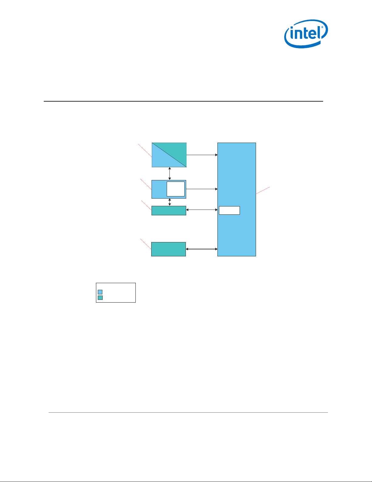
Transceiver
PLL IP Core
Master/Local
Clock
Generation
Block
Avalon-MM Master
Reset Ports
Analog and Digital
Reset Bus
Reconfiguration
Registers
Avalon-MM
Interface
Non-Bonded and
Bonded Clocks
Transceiver PHY IP Core
(1)
Note:
Transceiver PHY
Reset Controller
(2)
Legend:
Intel generated IP block
User created IP block
MAC IP Core /
Data Generator /
Data Analyzer
Parallel Data Bus
Avalon master allows access to Avalon-MM
reconfiguration registers via the Avalon
Memory Mapped interface. It enables PCS,
PMA , and PLL reconfiguration. To access
the reconfiguration registers, implement an
Avalon master in the FPGA fabric. This faciliates
reconfiguration by performing reads and writes
through the Avalon-MM interface.
Transceiver PLL IP core provides a clock source
to clock networks that drive the transceiver
channels. In Arria 10 devices, PLL IP Core
is separate from the transceiver PHY IP core.
Reset controller is used for resetting the
transceiver channels.
This block can be either a MAC IP core, or
a frame generator / analyzer or a
data generator / analyzer.
Transceiver PHY IP core controls the PCS and
PMA configurations and transceiver
channels functions for all communication
protocols.
(1) The Transceiver PHY IP core can be one of the supported PHY IP Cores ( For example: Native PHY IP Core, XAUI PHY IP Core, and so on)
(2) You can either design your own reset controller or use the Transceiver PHY Reset Controller.
UG-01143 | 2018.06.15
2. Implementing Protocols in Arria 10 Transceivers
2.1. Transceiver Design IP Blocks
Figure 18. Arria 10 Transceiver Design Fundamental Building Blocks
Intel Corporation. All rights reserved. Intel, the Intel logo, Altera, Arria, Cyclone, Enpirion, MAX, Nios, Quartus
and Stratix words and logos are trademarks of Intel Corporation or its subsidiaries in the U.S. and/or other
countries. Intel warrants performance of its FPGA and semiconductor products to current specifications in
accordance with Intel's standard warranty, but reserves the right to make changes to any products and services
at any time without notice. Intel assumes no responsibility or liability arising out of the application or use of any
information, product, or service described herein except as expressly agreed to in writing by Intel. Intel
customers are advised to obtain the latest version of device specifications before relying on any published
information and before placing orders for products or services.
*Other names and brands may be claimed as the property of others.
ISO
9001:2008
Registered
Page 33
Generate PHY IP Core
Connect Transceiver Datapath to MAC IP Core or to a Data Generator / Analyzer
Select PLL IP Core
Generate the Transceiver PHY Reset Controller
or create your own User-Coded Reset Controller
Compile Design
Verify Design Functionality
Generate PLL IP Core
Configure the PHY IP Core
Select PHY IP Core
Configure the PLL IP Core
Connect PHY IP Core to PLL IP Core, Reset Controller, and
connect reconfiguration logic via Avalon-MM interface
Create reconfiguration logic
(if needed)
Make analog parameter settings to I/O pins using the Assignment Editor or updating the Quartus Prime Settings File
2. Implementing Protocols in Arria 10 Transceivers
UG-01143 | 2018.06.15
2.2. Transceiver Design Flow
Figure 19. Transceiver Design Flow
Note: The design examples on the Intel FPGA wiki page provide useful guidance for developing your own design.
However, the content on the Intel FPGA wiki page is not guaranteed by Intel.
2.2.1. Select and Instantiate the PHY IP Core
Related Information
http://www.alterawiki.com
Select the appropriate PHY IP core to implement your protocol.
Refer to the Arria 10 Transceiver Protocols and PHY IP Support section to decide which
PHY IP to select to implement your protocol.
Intel® Arria® 10 Transceiver PHY User Guide
33
Page 34

2. Implementing Protocols in Arria 10 Transceivers
UG-01143 | 2018.06.15
You can create your Quartus® Prime project first, and then instantiate the various IPs
required for your design. In this case, specify the location to save your IP HDL files.
The current version of the PHY IP does not have the option to set the speed grade.
Specify the device family and speed grade when you create the Quartus Prime project.
You can also instantiate the PHY IP directly to evaluate the various features.
To instantiate a PHY IP:
1. Open the Quartus Prime software.
2.
Click Tools ➤ IP Catalog.
3. At the top of the IP Catalog window, select Arria 10 device family
4.
In IP Catalog, under Library ➤ Interface Protocols, select the appropriate PHY
IP and then click Add.
5. In the New IP Instance Dialog Box, provide the IP instance name.
6. Select Arria 10 device family.
7. Select the appropriate device and click OK.
The PHY IP Parameter Editor window opens.
Intel® Arria® 10 Transceiver PHY User Guide
34
Page 35
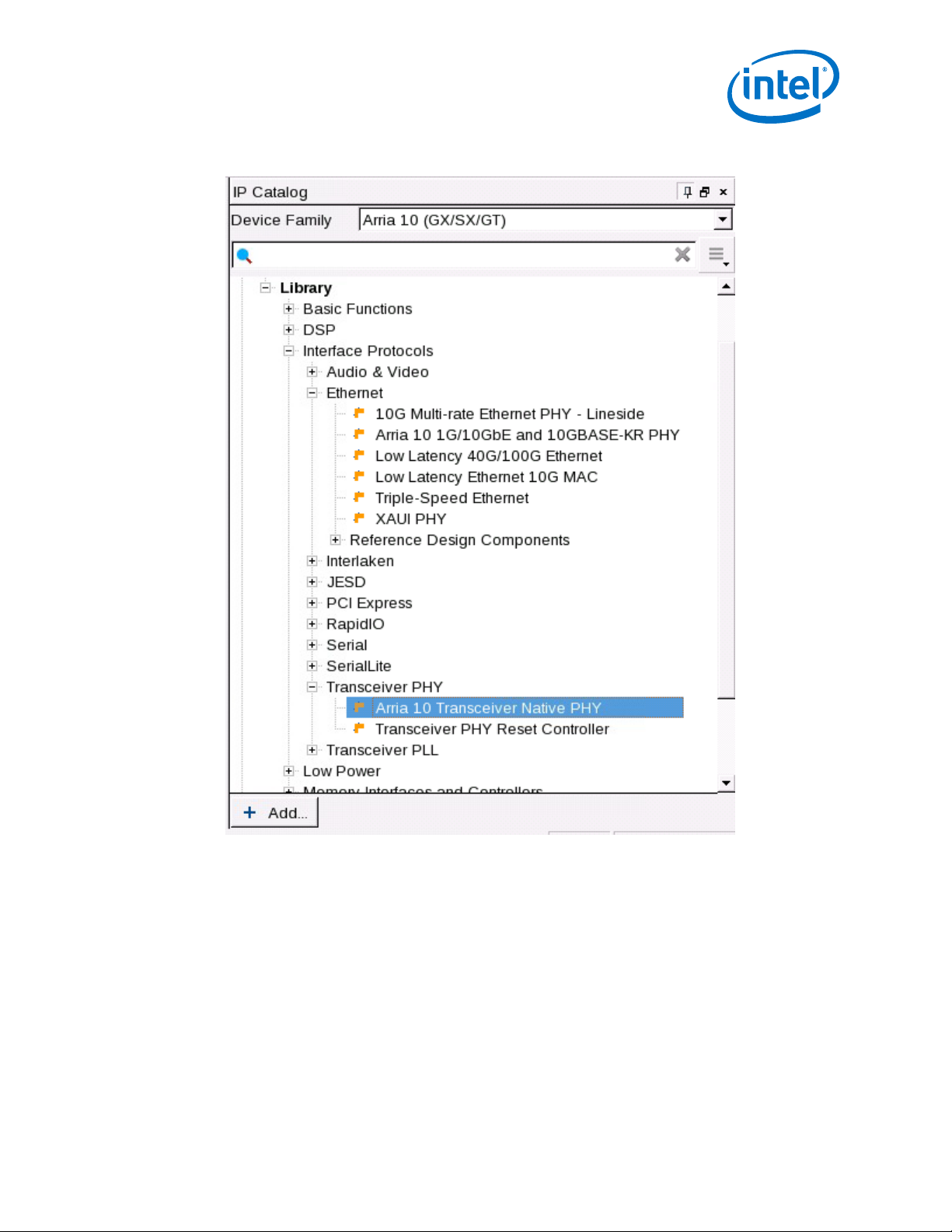
2. Implementing Protocols in Arria 10 Transceivers
UG-01143 | 2018.06.15
Figure 20. Arria 10 Transceiver PHY Types
Related Information
Arria 10 Transceiver Protocols and PHY IP Support on page 41
2.2.2. Configure the PHY IP Core
Configure the PHY IP core by selecting the valid parameters for your design. The valid
parameter settings are different for each protocol. Refer to the appropriate protocol's
section for selecting valid parameters for each protocol.
Related Information
• Using the Arria 10 Transceiver Native PHY IP Core on page 45
For information on Native PHY IP.
Intel® Arria® 10 Transceiver PHY User Guide
35
Page 36

• Interlaken on page 94
• Gigabit Ethernet (GbE) and GbE with IEEE 1588v2 on page 112
• 10GBASE-R, 10GBASE-R with IEEE 1588v2, and 10GBASE-R with FEC Variants on
page 124
• 10GBASE-KR PHY IP Core on page 135
• 1-Gigabit/10-Gigabit Ethernet (GbE) PHY IP Core on page 164
• PCI Express (PIPE) on page 229
• CPRI on page 279
• Using the "Basic (Enhanced PCS)" and "Basic with KR FEC" Configurations of
Enhanced PCS on page 289
• Using the Basic/Custom, Basic/Custom with Rate Match Configurations of Standard
PCS on page 300
• Design Considerations for Implementing Arria 10 GT Channels on page 319
2.2.3. Generate the PHY IP Core
After configuring the PHY IP, complete the following steps to generate the PHY IP.
1. Click the Generate HDL button in the Parameter Editor window. The
Generation dialog box opens.
2.
In Synthesis options, under Create HDL design for synthesis select Verilog
or VHDL.
3. Select appropriate Simulation options depending on the choice of the hardware
description language you selected under Synthesis options.
4. In Output Directory, select Clear output directories for selected generation
targets if you want to clear any previous IP generation files from the selected
output directory.
5. Click Generate.
2. Implementing Protocols in Arria 10 Transceivers
UG-01143 | 2018.06.15
The Quartus Prime software generates a <phy ip instance name> folder, <phy ip
instance name>_sim folder, <phy ip instance name>.qip file, <phy ip instance
name>.qsys file, and <phy ip instance name>.v file or <phy ip instance name>.vhd
file. This <phy ip instance name>.v file is the top level design file for the PHY IP and is
placed in the <phy ip instance name>/synth folder. The other folders contain lower
level design files used for simulation and compilation.
Related Information
IP Core File Locations on page 91
For more information about IP core file structure
2.2.4. Select the PLL IP Core
Arria 10 devices have three types of PLL IP cores:
• Advanced Transmit (ATX) PLL IP core.
• Fractional PLL (fPLL) IP core.
• Channel PLL / Clock Multiplier Unit (CMU) PLL IP core.
Intel® Arria® 10 Transceiver PHY User Guide
36
Page 37

2. Implementing Protocols in Arria 10 Transceivers
UG-01143 | 2018.06.15
Select the appropriate PLL IP for your design. For additional details, refer to the PLLs
and Clock Networks chapter.
To instantiate a PLL IP:
1. Open the Quartus Prime software.
2.
Click Tools ➤ IP Catalog.
3. At the top of the IP Catalog window, select Arria 10 device family
4.
In IP Catalog, under Library ➤ Basic Functions ➤ Clocks, PLLs, and Resets
➤ PLL choose the PLL IP (Arria 10 fPLL, Arria 10 Transceiver ATX PLL, or
Arria 10 Transceiver CMU PLL) you want to include in your design and then
click Add.
5. In the New IP Instance Dialog Box, provide the IP instance name.
6. Select Arria 10 device family.
7. Select the appropriate device and click OK.
The PLL IP GUI window opens.
Intel® Arria® 10 Transceiver PHY User Guide
37
Page 38

Figure 21. Arria 10 Transceiver PLL Types
2. Implementing Protocols in Arria 10 Transceivers
UG-01143 | 2018.06.15
Related Information
PLLs on page 349
2.2.5. Configure the PLL IP Core
Understand the available PLLs, clock networks, and the supported clocking
configurations. Configure the PLL IP to achieve the adequate data rate for your design.
Intel® Arria® 10 Transceiver PHY User Guide
38
Page 39

2. Implementing Protocols in Arria 10 Transceivers
UG-01143 | 2018.06.15
Related Information
• ATX PLL IP Core on page 354
• fPLL IP Core on page 362
• CMU PLL IP Core on page 370
• Using PLLs and Clock Networks on page 398
2.2.6. Generate the PLL IP Core
After configuring the PLL IP core, complete the following steps to generate the PLL IP
core.
1. Click the Generate HDL button in the Parameter Editor window. The
Generation dialog box opens.
2.
In Synthesis options, under Create HDL design for synthesis select Verilog
or VHDL.
3. Select appropriate Simulation options depending on the choice of the hardware
description language you selected under Synthesis options.
4. In Output Directory, select Clear output directories for selected generation
targets if you want to clear any previous IP generation files from the selected
output directory.
5. Click Generate.
The Quartus ® Prime software generates a <pll ip core instance name> folder, <pll ip
core instance name>_sim folder, <pll ip core instance name>.qip file, <pll ip core
instance name>.qsys, and <pll ip core instance name>.v file or <pll ip core instance
name>.vhd file. The <pll ip core instance name>.v file is the top level design file for
the PLL IP core and is placed in the <pll ip core instance name>/ synth folder. The
other folders contain lower level design files used for simulation and compilation.
Related Information
IP Core File Locations on page 91
For more information about IP core file structure
2.2.7. Reset Controller
There are two methods to reset the transceivers in Arria 10 devices:
• Use the Transceiver PHY Reset Controller.
• Create your own reset controller that follows the recommended reset sequence.
Related Information
Resetting Transceiver Channels on page 416
2.2.8. Create Reconfiguration Logic
Dynamic reconfiguration is the ability to dynamically modify the transceiver channels
and PLL settings during device operation. To support dynamic reconfiguration, your
design must include an Avalon master that can access the dynamic reconfiguration
registers using the Avalon-MM interface.
Intel® Arria® 10 Transceiver PHY User Guide
39
Page 40

2. Implementing Protocols in Arria 10 Transceivers
UG-01143 | 2018.06.15
The Avalon-MM master enables PLL and channel reconfiguration. You can dynamically
adjust the PMA parameters, such as differential output voltage swing (Vod), and preemphasis settings. This adjustment can be done by writing to the Avalon-MM
reconfiguration registers through the user generated Avalon-MM master.
For detailed information on dynamic reconfiguration, refer to Reconfiguration Interface
and Dynamic Reconfiguration chapter.
Related Information
Reconfiguration Interface and Dynamic Reconfiguration on page 502
2.2.9. Connect the PHY IP to the PLL IP Core and Reset Controller
Connect the PHY IP, PLL IP core, and the reset controller. Write the top level module to
connect all the IP blocks.
All of the I/O ports for each IP, can be seen in the <phy instance name>.v file or <phy
instance name>.vhd, and in the <phy_instance_name>_bb.v file.
For more information about description of the ports, refer to the ports tables in the
PLLs, Using the Transceiver Native PHY IP Core, and Resetting Transceiver Channels
chapters.
Related Information
• Enhanced PCS Ports on page 76
• Standard PCS Ports on page 86
• Resetting Transceiver Channels on page 416
• Using the Arria 10 Transceiver Native PHY IP Core on page 45
• PLLs and Clock Networks on page 347
2.2.10. Connect Datapath
Connect the transceiver PHY layer design to the Media Access Controller (MAC) IP core
or to a data generator / analyzer or a frame generator / analyzer.
2.2.11. Make Analog Parameter Settings
Make analog parameter settings to I/O pins using the Assignment Editor or updating
the Quartus Prime Settings File.
After verifying your design functionality, make pin assignments and PMA analog
parameter settings for the transceiver pins.
1. Assign FPGA pins to all the transceiver and reference clock I/O pins. For more
details, refer to the Arria 10 Pin Connection Guidelines.
2. Set the analog parameters to the transmitter, receiver, and reference clock pins
using the Assignment Editor.
All of the pin assignments and analog parameters set using the Pin Planner and
the Assignment Editor are saved in the <top_level_project_name>.qsf file. You
can also directly modify the Quartus Settings File (.qsf) to set PMA analog
parameters.
Intel® Arria® 10 Transceiver PHY User Guide
40
Page 41

2. Implementing Protocols in Arria 10 Transceivers
UG-01143 | 2018.06.15
Related Information
• Analog Parameter Settings on page 585
• Arria 10 Pin Connection Guidelines
2.2.12. Compile the Design
To compile the transceiver design, add the <phy_instancename>.qip files for all the IP
blocks generated using the IP Catalog to the Quartus Prime project library. You can
alternatively add the .qsys and .qip variants of the IP cores.
Note: If you add both the .qsys and the .qip file into the Quartus Prime project, the
software generates an error.
Related Information
Intel Quartus Prime Incremental Compilation for Hierarchical and Team-Based Design
For more information about compilation details.
2.2.13. Verify Design Functionality
Simulate your design to verify the functionality of your design. For more details, refer
to Simulating the Native Transceiver PHY IP Core section.
Related Information
• Simulating the Transceiver Native PHY IP Core on page 325
• Quartus Prime Handbook - Volume 3: Verification
Information about design simulation and verification.
2.3. Arria 10 Transceiver Protocols and PHY IP Support
Table 8. Arria 10 Transceiver Protocols and PHY IP Support
Protocol Transceiver PHY IP
PCIe Gen3 x1, x2, x4,x8Native PHY IP core
PCIe Gen2 x1, x2, x4,x8Native PHY IP (PIPE)
PCIe Gen1 x1, x2, x4,x8Native PHY IP (PIPE)
(9)
For more information about Transceiver Configuration Rules, refer to Using the Intel Arria
Core
(PIPE)/Hard IP for PCI
core/Hard IP for PCI
core/Hard IP for PCI
Express
Express
Express
(11)
(11)
(11)
10Transceiver Native PHY IP Core section.
(10)
For more information about Protocol Presets, refer to Using the Intel Arria 10Transceiver
Native PHY IP Core section.
(11)
Hard IP for PCI Express is also available as a separate IP core.
PCS Support Transceiver
Configuration Rule
Standard and Gen3 Gen3 PIPE PCIe PIPE Gen3 x1
Standard Gen2 PIPE PCIe PIPE Gen2 x1
Standard Gen1 PIPE User created
(9)
Protocol Preset
PCIe PIPE Gen3 x8
PCIe PIPE Gen2 x8
continued...
(10)
Intel® Arria® 10 Transceiver PHY User Guide
41
Page 42

2. Implementing Protocols in Arria 10 Transceivers
UG-01143 | 2018.06.15
Protocol Transceiver PHY IP
1000BASE-X Gigabit
Ethernet
1000BASE-X Gigabit
Ethernet with 1588
10GBASE-R Native PHY IP core Enhanced 10GBASE-R 10GBASE-R Low
10GBASE-R 1588 Native PHY IP core Enhanced 10GBASE-R 1588 10GBASE-R 1588
10GBASE-R with KR
FEC
10GBASE-KR and
1000BASE-X
40GBASE-R Native PHY IP core Enhanced Basic (Enhanced PCS) Low Latency Enhanced
40GBASE-R with FEC/
40GBASE-KR4
100GBASE-R via
CAUI-4/CPPI-4/BP and
CEI-25G
100GBASE-R via CAUI Native PHY IP core Enhanced Basic (Enhanced PCS) Low Latency Enhanced
100GBASE-R via CAUI
with FEC
XAUI XAUI PHY IP core Soft PCS Not applicable Not applicable
SPAUI Native PHY IP core Standard and
(14)
Core
Native PHY IP core Standard GbE GIGE - 1.25 Gbps
Native PHY IP core Standard GbE 1588 GIGE - 1.25 Gbps
Native PHY IP core Enhanced 10GBASE-R w/KR FEC 10GBASE-R w/KR FEC
1G/10GbE and
10GBASE-KR PHY
(12)
IP
Native PHY IP core Enhanced Basic w/KR FEC User created
Native PHY IP core Enhanced and PCS
Native PHY IP core Enhanced Basic w/KR FEC User created
PCS Support Transceiver
Standard and
Enhanced
Direct
Enhanced
Configuration Rule
Not applicable BackPlane_wo_1588
Basic (Enhanced
PCS) / PCS Direct
Basic/Custom
(Standard PCS)
Protocol Preset
(9)
1588
Latency
LineSide (optical)
LineSide(optical)_158
PCS
Low Latency GT
PCS
User created
continued...
(10)
8
(13)
(15)
(16)
(9)
For more information about Transceiver Configuration Rules, refer to Using the Intel Arria
10Transceiver Native PHY IP Core section.
(10)
For more information about Protocol Presets, refer to Using the Intel Arria 10Transceiver
Native PHY IP Core section.
(12)
The 1G/10GbE and 10GBASE-KR PHY IP core includes the necessary soft IP for link training,
auto speed negotiation, and sequencer functions.
(13)
To implement 40GBASE-R using the Low Latency Enhanced PCS preset, change the number of
data channels to four and select appropriate PCS- FPGA Fabric and PCS-PMA width.
(14)
Link training, auto speed negotiation and sequencer functions are not included in the Native
PHY IP. The user would have to create soft logic to implement these functions when using
Native PHY IP.
(15)
Low Latency GT protocol preset requires some modification to implement CAUI-4/CPPI-4/BP-4
and CEI-25G.
(16)
To implement 100GBASE-R via CAUI using the Low Latency Enhanced PCS preset, change the
number of data channels to 10 and select appropriate PCS-FPGA Fabric and PCS-PMA width.
Intel® Arria® 10 Transceiver PHY User Guide
42
Page 43

2. Implementing Protocols in Arria 10 Transceivers
UG-01143 | 2018.06.15
Protocol Transceiver PHY IP
DDR XAUI Native PHY IP core Standard and
Interlaken (CEI-6G/
OTU-4 (100G) via
OTL4.10/OIF SFI-S
OTU-3 (40G) via
OTL3.4/OIF SFI-5.2/
OTU-2 (10G) via SFP
+/SFF-8431/CEI-11G
OTU-2 (10G) via OIF
SONET/SDH STS-768/
STM-256 (40G) via
OIF SFI-5.2/STL256.4
SONET/SDH STS-768/
STM-256 (40G) via
SONET/SDH STS-192/
STM-64 (10G) via SFP
+/SFF-8431/CEI-11G
SONET/SDH STS-192/
STM-64 (10G) via OIF
SFI-5.1s/SxI-5/
SONET STS-96 (5G)
via OIF SFI-5.1s
(17)
11G)
SFI-5.1
SFI-5.1s
OTU-1 (2.7G) Native PHY IP core Standard Basic/Custom
OIF SFI-5.1
SFI-4.2
Core
Native PHY IP core Enhanced Interlaken Interlaken
Native PHY IP core Enhanced Basic (Enhanced PCS) SFI-S 64:64 4x11.3
Native PHY IP core Enhanced Basic (Enhanced PCS) User created
Native PHY IP core Enhanced Basic (Enhanced PCS) User created
Native PHY IP core Enhanced Basic (Enhanced PCS) User created
Native PHY IP core Enhanced Basic (Enhanced PCS) User created
Native PHY IP core Enhanced Basic (Enhanced PCS) User created
Native PHY IP core Enhanced Basic (Enhanced PCS) User created
Native PHY IP core Enhanced Basic (Enhanced PCS) User created
Native PHY IP core Enhanced Basic/Custom
PCS Support Transceiver
Enhanced
Configuration Rule
Basic (Enhanced PCS)
Basic/Custom
(Standard PCS)
Basic (Enhanced PCS)
(Standard PCS)
(Standard PCS)
Protocol Preset
(9)
User created
10x12.5Gbps
6x10.3Gbps
1x6.25Gbps
User created
SONET/SDH OC-96
Interlaken
Interlaken
(18)
Gbps
continued...
(10)
(9)
For more information about Transceiver Configuration Rules, refer to Using the Intel Arria
10Transceiver Native PHY IP Core section.
(10)
For more information about Protocol Presets, refer to Using the Intel Arria 10Transceiver
Native PHY IP Core section.
(17)
A Transmit PCS soft bonding logic required for multi-lane bonding configuration is provided in
the design example.
(18)
To implement OTU-4 (100G) via OTL4.10/OIF SFI-S using SFI-S 64:64 4x11.3Gbps preset,
change the number of data channels to 10 for OTL4.10 or user desired number of channels
and datarate implemented for SFI-S.
Intel® Arria® 10 Transceiver PHY User Guide
43
Page 44

2. Implementing Protocols in Arria 10 Transceivers
UG-01143 | 2018.06.15
Protocol Transceiver PHY IP
SONET/SDH STS-48/
STM-16 (2.5G) via
SFP/TFI-5.1
SONET/SDH STS-12/
STM-4 (0.622G) via
SFP/TFI-5.1
Intel QPI 1.1/2.0 Native PHY IP core PCS Direct PCS Direct User created
SD-SDI/HD-SDI/3G-
SDI
Vx1 Native PHY IP core Standard Basic/Custom
DisplayPort
1.25G/ 2.5G
10G GPON/EPON
2.5G/1.25G GPON/
16G/10G Fibre
8G/4G/2G/1G Fibre
EDR Infiniband x1, x4 Native PHY IP core Enhanced (low latency
FDR/FDR-10 Infiniband
x1, x4, x12
SDR/DDR/QDR
Infiniband x1, x4, x12
CPRI v6.1 12.16512/
CPRI v6.0 10.1376 Gbps
CPRI 4.2/OBSAI RP3
(20)
EPON
Channel
Channel
v4.2
Core
Native PHY IP core Standard Basic/Custom
Native PHY IP core
Native PHY IP core Standard Basic/Custom
Native PHY IP core Standard Basic/Custom
Native PHY IP core Enhanced Basic (Enhanced PCS) User created
Native PHY IP core Standard Basic/Custom
Native PHY IP core Enhanced Basic (Enhanced PCS) User created
Native PHY IP core Standard Basic/Custom
Native PHY IP core Enhanced Basic (Enhanced PCS) User created
Native PHY IP core Standard Basic/Custom
Native PHY IP core Enhanced 10GBASE-R 1588
Native PHY IP core Standard CPRI (Auto) / CPRI
(19)
PCS Support Transceiver
Standard Basic/Custom
mode)
PCS Direct
Configuration Rule
(Standard PCS)
(Standard PCS)
(Standard PCS)
(Standard PCS)
(Standard PCS)
(Standard PCS)
(Standard PCS)
Basic (Enhanced PCS)
PCS Direct
(Standard PCS)
10GBASE-R
(Manual)
Protocol Preset
(9)
SONET/SDH OC-48
SONET/SDH OC-12
3G/HD SDI NTSC
3G/HD SDI PAL
User created
User created
User created
User created
User created
User created
User created
CPRI 9.8Gbps Auto
(10)
Mode
continued...
(9)
For more information about Transceiver Configuration Rules, refer to Using the Intel Arria
10Transceiver Native PHY IP Core section.
(10)
For more information about Protocol Presets, refer to Using the Intel Arria 10Transceiver
Native PHY IP Core section.
(19)
The minimum operational data rate is 1.0 Gbps for both the transmitter and receiver. For
transmitter data rates less than 1.0 Gbps, oversampling must be applied at the transmitter.
For receiver data rates less than 1.0 Gbps, oversampling must be applied at the receiver.
(20)
To meet DisplayPort TX electrical full compliance to VESA DisplayPort Standard version 1.3 and
VESA DisplayPort PHY Compliance Specification version 1.2b , VCCT_GXB & VCCR_GXB needs
to be 1.03V or higher. Test Refer to AN745: Design Guidelines for DisplayPort and HDMI
Interfaces for further details.
Intel® Arria® 10 Transceiver PHY User Guide
44
Page 45

2. Implementing Protocols in Arria 10 Transceivers
UG-01143 | 2018.06.15
Protocol Transceiver PHY IP
SRIO 2.2/1.3 Native PHY IP core Standard Basic/Custom with
SAS 3.0 Native PHY IP core Enhanced Basic (Enhanced PCS) User created
SATA 3.0/2.0/1.0 and
SAS 2.0/1.1/1.0
HiGig/HiGig+/HiGig2/
HiGig2+
JESD204A / JESD204B Native PHY IP core Standard and
ASI Native PHY IP core Standard Basic/Custom
SPI-5 (100G) / SPI-5
(50G)
Custom and other
protocols
Core
Native PHY IP core Standard Basic/Custom
Native PHY IP core Standard Basic/Custom
Native PHY IP core Enhanced Basic (Enhanced PCS) User created
Native PHY IP core Standard and
PCS Support Transceiver
Enhanced
Enhanced
PCS Direct
Configuration Rule
Rate Match(Standard
PCS)
(Standard PCS)
(Standard PCS)
Basic/Custom
(Standard PCS) Basic
(Enhanced PCS)
(Standard PCS)
Basis/Custom
(Standard PCS)
Basic (Enhanced PCS)
Basic/Custom with
Rate Match (Standard
PCS)
PCS Direct
Protocol Preset
(9)
CPRI 9.8 Gbps Manual
(21)
(10)
Mode
Serial Rapid IO 1.25
Gbps
SAS Gen2/Gen1.1/
Gen1
SATA Gen3/Gen2/
Gen1
User created
User created
User created
User created
Related Information
• Using the Arria 10 Transceiver Native PHY IP Core on page 45
• AN745: Design Guidelines for DisplayPort and HDMI Interfaces
2.4. Using the Arria 10 Transceiver Native PHY IP Core
This section describes the use of the Intel-provided Arria 10 Transceiver Native PHY IP
core. This Native PHY IP core provides direct access to Arria 10 transceiver PHY
features.
Use the Native PHY IP core to configure the transceiver PHY for your protocol
implementation. To instantiate the IP, click Tools ➤ IP Catalog to select your IP core
variation. Use the Parameter Editor to specify the IP parameters and configure the
PHY IP for your protocol implementation. To quickly configure the PHY IP, select a
(9)
For more information about Transceiver Configuration Rules, refer to Using the Intel Arria
10Transceiver Native PHY IP Core section.
(10)
For more information about Protocol Presets, refer to Using the Intel Arria 10Transceiver
Native PHY IP Core section.
(21)
For JESD204B, Enhanced PCS is used when the data rate is above 12.0 Gbps
Intel® Arria® 10 Transceiver PHY User Guide
45
Page 46

Reconfiguration
Registers
Enhanced PCS
Transmit and Receive Clocks
Standard PCS
PCIe Gen3
PCS
Transmit
PMA
Receive
PMA
Reset Signals
Transmit Parallel Data
Reconfiguration Interface
Transmit Serial Data
Receive Serial Data
Receive Parallel Data
PCS-Direct
Nios II
Calibration
Calibration Signals
2. Implementing Protocols in Arria 10 Transceivers
UG-01143 | 2018.06.15
preset that matches your protocol configuration as a starting point. Presets are PHY IP
configuration settings for various protocols that are stored in the IP Parameter
Editor. Presets are explained in detail in the Presets section below.
You can also configure the PHY IP by selecting an appropriate Transceiver
Configuration Rule. The transceiver configuration rules check the valid combinations
of the PCS and PMA blocks in the transceiver PHY layer, and report errors or warnings
for any invalid settings.
Use the Native PHY IP core to instantiate the following PCS options:
• Standard PCS
• Enhanced PCS
• PCIe Gen3 PCS
• PCS Direct
Based on the Transceiver Configuration Rule that you select, the PHY IP core selects
the appropriate PCS. The PHY IP core allows you to select all the PCS blocks if you
intend to dynamically reconfigure from one PCS to another. Refer to General and
Datapath Parameters section for more details on how to enable PCS blocks for
dynamic reconfiguration. Refer to the How to Place Channels for PIPE Configuration
section or the PCIE solutions guides on restrictions on placement of transceiver
channels next to active banks with PCI Express interfaces that are Gen3 capable..
After you configure the PHY IP core in the Parameter Editor, click Generate HDL to
generate the IP instance. The top level file generated with the IP instance includes all
the available ports for your configuration. Use these ports to connect the PHY IP core
to the PLL IP core, the reset controller IP core, and to other IP cores in your design.
Figure 22. Native PHY IP Core Ports and Functional Blocks
Intel® Arria® 10 Transceiver PHY User Guide
46
Page 47

Documentation
Presets
General
Options
Common
PMA Options
Datapath
Options
PMA/PCS, Dynamic Reconfiguration, Optional Analog PMA Settings, and General Options
2. Implementing Protocols in Arria 10 Transceivers
UG-01143 | 2018.06.15
Figure 23. Native PHY IP Core Parameter Editor
Note: Although the Quartus Prime software provides legality checks, the supported FPGA
fabric to PCS interface widths and the supported data rates are pending
characterization.
Related Information
• Configure the PHY IP Core on page 35
• Interlaken on page 94
• Gigabit Ethernet (GbE) and GbE with IEEE 1588v2 on page 112
• 10GBASE-R, 10GBASE-R with IEEE 1588v2, and 10GBASE-R with FEC Variants on
page 124
• 10GBASE-KR PHY IP Core on page 135
• 1-Gigabit/10-Gigabit Ethernet (GbE) PHY IP Core on page 164
• PCI Express (PIPE) on page 229
• CPRI on page 279
• Using the "Basic (Enhanced PCS)" and "Basic with KR FEC" Configurations of
Enhanced PCS on page 289
• Using the Basic/Custom, Basic/Custom with Rate Match Configurations of Standard
PCS on page 300
• Design Considerations for Implementing Arria 10 GT Channels on page 319
• PMA Parameters on page 51
• Presets on page 48
• General and Datapath Parameters on page 48
• Enhanced PCS Ports on page 76
• Standard PCS Ports on page 86
• PMA Ports on page 73
• How to Place Channels for Pipe Configuration on page 268
Intel® Arria® 10 Transceiver PHY User Guide
47
Page 48

2. Implementing Protocols in Arria 10 Transceivers
2.4.1. Presets
You can select preset settings for the Native PHY IP core defined for each protocol. Use
presets as a starting point to specify parameters for your specific protocol or
application.
To apply a preset to the Native PHY IP core, double-click on the preset name. When
you apply a preset, all relevant options and parameters are set in the current instance
of the Native PHY IP core. For example, selecting the Interlaken preset enables all
parameters and ports that the Interlaken protocol requires.
Selecting a preset does not prevent you from changing any parameter to meet the
requirements of your design. Any changes that you make are validated by the design
rules for the transceiver configuration rules you specified, not the selected preset.
Note: Selecting a preset clears any prior selections user has made so far.
2.4.2. General and Datapath Parameters
You can customize your instance of the Native PHY IP core by specifying parameter
values. In the Parameter Editor, the parameters are organized in the following
sections for each functional block and feature:
• General, Common PMA Options, and Datapath Options
• TX PMA
• RX PMA
• Standard PCS
• Enhanced PCS
• PCS Direct Datapath
• Dynamic Reconfiguration
• Analog PMA Settings (Optional)
• Generation Options
UG-01143 | 2018.06.15
Table 9. General, Common PMA Options, and Datapath Options
Parameter Value Description
Message level for rule
violations
VCCR_GXB and
VCCT_GXB supply voltage
for the Transceiver
Transceiver Link Type sr, lr Selects the type of transceiver link. sr-Short Reach (Chip-to-chip
(22)
Although you can generate the PHY with warnings, you can not compile the PHY in Quartus
error
warning
0_9V, 1_0V, 1_1V
Specifies the messaging level for parameter rule violations.
Selecting error causes all rule violations to prevent IP generation.
Selecting warning displays all rule violations as warnings in the
message window and allows IP generation despite the violations.
(22)
Selects the VCCR_GXB and VCCT_GXB supply voltage for the
Transceiver.
Note: This option is only used for GUI rule validation. Use
Quartus Prime Setting File (.qsf) assignments to set this
parameter in your static design.
communication), lr-Long Reach (Backplane communication).
Prime.
Intel® Arria® 10 Transceiver PHY User Guide
48
continued...
Page 49

2. Implementing Protocols in Arria 10 Transceivers
UG-01143 | 2018.06.15
Parameter Value Description
Transceiver
configuration rules
PMA configuration
rules
Transceiver mode TX/RX Duplex
Number of data
channels
Data rate < valid Transceiver data
User Selection Specifies the valid configuration rules for the transceiver.
Basic
SATA/SAS
QPI
GPON
TX Simplex
RX Simplex
1 – <n> Specifies the number of transceiver channels to be implemented.
rate >
Note: This option is only used for GUI rule validation. Use
Quartus Prime Setting File (.qsf) assignments to set this
parameter in your static design.
This parameter specifies the configuration rule against which the
Parameter Editor checks your PMA and PCS parameter settings
for specific protocols. Depending on the transceiver configuration
rule selected, the Parameter Editor validates the parameters and
options selected by you and generates error messages or warnings
for all invalid settings.
To determine the transceiver configuration rule to be selected for
your protocol, refer to Table 8 on page 41 Transceiver
Configuration Rule Parameters table for more details about each
transceiver configuration rule.
This parameter is used for rule checking and is not a preset. You
need to set all parameters for your protocol implementation.
Specifies the configuration rule for PMA.
Select Basic for all other protocol modes except for SATA, GPON,
and QPI.
SATA (Serial ATA) can be used only if the Transceiver
configuration rule is set to Basic/Custom (Standard PCS).
GPON can be used only if the Transceiver configuration rule is
set to Basic (Enhanced PCS).
QPI can be used only if the Transceiver configuration rule is
set to PCS Direct.
Specifies the operational mode of the transceiver.
• TX/RX Duplex : Specifies a single channel that supports both
transmission and reception.
• TX Simplex : Specifies a single channel that supports only
transmission.
• RX Simplex : Specifies a single channel that supports only
reception.
The default is TX/RX Duplex.
The maximum number of channels available, ( <n> ), depends on
the package you select.
The default value is 1.
Specifies the data rate in megabits per second (Mbps).
continued...
Intel® Arria® 10 Transceiver PHY User Guide
49
Page 50
2. Implementing Protocols in Arria 10 Transceivers
UG-01143 | 2018.06.15
Parameter Value Description
Enable datapath and
interface
reconfiguration
Enable simplified data
interface
Provide separate
interface for each
channel
On/Off When you turn this option on, you can preconfigure and
On/Off
dynamically switch between the Standard PCS, Enhanced PCS, and
PCS direct datapaths.
The default value is Off.
By default, all 128-bits are ports for the tx_parallel_data and
rx_parallel_data buses are exposed. You must understand the
mapping of data and control signals within the interface. Refer to
the Enhanced PCS TX and RX Control Ports section for details
about mapping of data and control signals.
When you turn on this option, the Native PHY IP core presents a
simplified data and control interface between the FPGA fabric and
transceiver. Only the sub-set of the 128-bits that are active for a
particular FPGA fabric width are ports.
The default value is Off.
On/Off When selected the Native PHY IP core presents separate data,
reset and clock interfaces for each channel rather than a wide bus.
(23)
Table 10. Transceiver Configuration Rule Parameters
Transceiver Configuration Setting Description
Basic/Custom (Standard PCS) Enforces a standard set of rules within the Standard PCS. Select these rules to
Basic/Custom w /Rate Match
(Standard PCS)
CPRI (Auto) Enforces rules required by the CPRI protocol. The receiver word aligner mode is
CPRI (Manual) Enforces rules required by the CPRI protocol. The receiver word aligner mode is
GbE Enforces rules that the 1 Gbps Ethernet (1 GbE) protocol requires.
GbE 1588 Enforces rules for the 1 GbE protocol with support for Precision time protocol
Gen1 PIPE Enforces rules for a Gen1 PCIe ® PIPE interface that you can connect to a soft
Gen2 PIPE Enforces rules for a Gen2 PCIe PIPE interface that you can connect to a soft MAC
Gen3 PIPE Enforces rules for a Gen3 PCIe PIPE interface that you can connect to a soft MAC
Basic (Enhanced PCS) Enforces a standard set of rules within the Enhanced PCS. Select these rules to
Interlaken Enforces rules required by the Interlaken protocol.
10GBASE-R Enforces rules required by the 10GBASE-R protocol.
implement custom protocols requiring blocks within the Standard PCS or
protocols not covered by the other configuration rules.
Enforces a standard set of rules including rules for the Rate Match FIFO within
the Standard PCS. Select these rules to implement custom protocols requiring
blocks within the Standard PCS or protocols not covered by the other
configuration rules.
set to Auto. In Auto mode, the word aligner is set to deterministic latency.
set to Manual. In Manual mode, logic in the FPGA fabric controls the word
aligner.
(PTP) as defined in the IEEE 1588 Standard.
MAC and Data Link Layer.
and Data Link Layer.
and Data Link Layer.
implement protocols requiring blocks within the Enhanced PCS or protocols not
covered by the other configuration rules.
continued...
(23)
This option cannot be used, if you intend to dynamically reconfigure between PCS datapaths,
or reconfigure the interface of the transceiver.
Intel® Arria® 10 Transceiver PHY User Guide
50
Page 51

2. Implementing Protocols in Arria 10 Transceivers
UG-01143 | 2018.06.15
Transceiver Configuration Setting Description
10GBASE-R 1588 Enforces rules required by the 10GBASE-R protocol with 1588 enabled.
10GBASE-R w/KR FEC Enforces rules required by the 10GBASE-R protocol with KR FEC block enabled.
40GBASE-R w/KR FEC Enforces rules required by the 40GBASE-R protocol with the KR FEC block
Basic w/KR FEC Enforces a standard set of rules required by the Enhanced PCS when you enable
PCS Direct Enforces rules required by the PCS Direct mode. In this configuration the data
enabled.
the KR FEC block. Select this rule to implement custom protocols requiring
blocks within the Enhanced PCS or protocols not covered by the other
configuration rules.
flows through the PCS channel, but all the internal PCS blocks are bypassed. If
required, the PCS functionality can be implemented in the FPGA fabric.
Related Information
• Device Transceiver Layout on page 9
• Enhanced PCS TX and RX Control Ports on page 83
2.4.3. PMA Parameters
You can specify values for the following types of PMA parameters:
TX PMA
• TX Bonding Options
• TX PLL Options
• TX PMA Optional Ports
RX PMA
• RX CDR Options
• Equalization
• RX PMA Optional Ports
Table 11. TX Bonding Options
Parameter Value Description
TX channel bonding
mode
Not bonded
PMA only bonding
PMA and PCS bonding
Selects the bonding mode to be used for the channels specified.
Bonded channels use a single TX PLL to generate a clock that
drives multiple channels, reducing channel-to-channel skew. The
following options are available:
Not bonded: In a non-bonded configuration, only the high speed
serial clock is expected to be connected from the TX PLL to the
Native PHY IP core. The low speed parallel clock is generated by
the local clock generation block (CGB) present in the transceiver
channel. For non-bonded configurations, because the channels are
not related to each other and the feedback path is local to the PLL,
the skew between channels cannot be calculated.
PMA only bonding: In PMA bonding, the high speed serial clock
is routed from the transmitter PLL to the master CGB. The master
CGB generates the high speed and low parallel clocks and the local
CGB for each channel is bypassed. Refer to the Channel Bonding
section for more details.
PMA and PCS bonding : In a PMA and PCS bonded
configuration, the local CGB in each channel is bypassed and the
parallel clocks generated by the master CGB are used to clock the
continued...
Intel® Arria® 10 Transceiver PHY User Guide
51
Page 52

Parameter Value Description
PCS TX channel
bonding master
Actual PCS TX channel
bonding master
Auto, 0 to <number of
channels> -1
0 to <number of
channels> -1
Table 12. TX PLL Options
Parameter Value Description
TX local clock division
factor
Number of TX PLL
clock inputs per
channel
Initial TX PLL clock
input selection
1, 2, 4, 8 Specifies the value of the divider available in the transceiver
1, 2, 3 , 4 Specifies the number of TX PLL clock inputs per channel. Use this
0 to <number of TX
PLL clock inputs> -1
2. Implementing Protocols in Arria 10 Transceivers
UG-01143 | 2018.06.15
network. The master CGB generates both the high and low speed
clocks. The master channel generates the PCS control signals and
distributes to other channels through a control plane block.
The default value is Not bonded.
Refer to Channel Bonding section in PLLs and Clock Networks
chapter for more details.
Specifies the master PCS channel for PCS bonded configurations.
Each Native PHY IP core instance configured with bonding must
specify a bonding master. If you select Auto, the Native PHY IP
core automatically selects a recommended channel.
The default value is Auto. Refer to the PLLs and Clock Networks
chapter for more information about the TX channel bonding
master.
This parameter is automatically populated based on your selection
for the PCS TX channel bonding master parameter. Indicates
the selected master PCS channel for PCS bonded configurations.
channels to divide the TX PLL output clock to generate the correct
frequencies for the parallel and serial clocks.
parameter when you plan to dynamically switch between TX PLL
clock sources. Up to four input sources are possible.
Specifies the initially selected TX PLL clock input. This parameter
is necessary when you plan to switch between multiple TX PLL
clock inputs.
Table 13. TX PMA Optional Ports
Parameter Value Description
Enable
tx_pma_analog_reset_ack
port
Enable tx_pma_clkout port On/Off
Enable tx_pma_div_clkout
port
tx_pma_div_clkout division
factor
(24)
This clock should not be used to clock the FPGA - transceivers interface. This clock may be
On/Off
On/Off
Disabled, 1, 2,
33, 40, 66
Enables the optional tx_pma_analog_reset_ack output port.
This port should not be used for register mode data transfers.
Enables the optional tx_pma_clkout output clock. This is the low
speed parallel clock from the TX PMA. The source of this clock is
the serializer. It is driven by the PCS/PMA interface block.
Enables the optional tx_pma_div_clkout output clock. This
clock is generated by the serializer. You can use this to drive core
logic, to drive the FPGA - transceivers interface.
If you select a tx_pma_div_clkout division factor of 1 or 2,
this clock output is derived from the PMA parallel clock. If you
select a tx_pma_div_clkout division factor of 33, 40, or 66,
this clock is derived from the PMA high serial clock. This clock is
commonly used when the interface to the TX FIFO runs at a
different rate than the PMA parallel clock frequency, such as 66:40
applications.
Selects the division factor for the tx_pma_div_clkout output
clock when enabled.
(25)
used as a reference clock to an external clock cleaner.
(24)
continued...
Intel® Arria® 10 Transceiver PHY User Guide
52
Page 53

2. Implementing Protocols in Arria 10 Transceivers
UG-01143 | 2018.06.15
Parameter Value Description
Enable
tx_pma_iqtxrx_clkout port
Enable tx_pma_elecidle
port
Enable tx_pma_qpipullup
port (QPI)
Enable tx_pma_qpipulldn
port (QPI)
Enable tx_pma_txdetectrx
port (QPI)
Enable tx_pma_rxfound
port (QPI)
Enable rx_seriallpbken port On/Off
On/Off
On/Off
On/Off
On/Off
On/Off
On/Off
Enables the optional tx_pma_iqtxrx_clkout output clock. This
clock can be used to cascade the TX PMA output clock to the input
of a PLL.
Enables the tx_pma_elecidle port. When you assert this port,
the transmitter is forced into an electrical idle condition. This port
has no effect when the transceiver is configured for PCI Express.
Enables the tx_pma_qpipullup control input port. Use this port
only for Quick Path Interconnect (QPI) applications.
Enables the tx_pma_qpipulldn control input port. Use this port
only for QPI applications.
Enables the tx_pma_txdetectrx control input port. The receiver
detect block in the TX PMA detects the presence of a receiver at
the other end of the channel. After receiving a
tx_pma_txdetectrx request the receiver detect block initiates
the detection process. Use this port only in QPI applications.
Enables the tx_pma_rxfound status output port. The receiver
detect block in TX PMA detects the presence of a receiver at the
other end by using the tx_pma_txdetectrx input. The
tx_pma_rxfound port reports the status of the detection
operation. Use this port only in QPI applications.
Enables the optional rx_seriallpbken control input port. The
assertion of this signal enables the TX to RX serial loopback path
within the transceiver. This is an asynchronous input signal.
Table 14. RX CDR Options
Parameter Value Description
Number of CDR
reference clocks
Selected CDR
reference clock
Selected CDR
reference clock
frequency
PPM detector
threshold
1 - 5 Specifies the number of CDR reference clocks. Up to 5 sources are
0 to <number of CDR
reference clocks> -1
< data rate dependent > Specifies the CDR reference clock frequency. This value depends
100
300
500
1000
possible.
The default value is 1.
Use this feature when you want to dynamically re-configure CDR
reference clock source.
Specifies the initial CDR reference clock. This parameter
determines the available CDR references used.
The default value is 0.
on the data rate specified.
Specifies the PPM threshold for the CDR. If the PPM between the
incoming serial data and the CDR reference clock, exceeds this
threshold value, the CDR loses lock.
The default value is 1000.
Table 15. Equalization
Parameters Value Description
CTLE adaptation mode Manual Specifies the Continuous Time Linear Equalization (CTLE)
operation mode.
continued...
(25)
The default value is Disabled.
Intel® Arria® 10 Transceiver PHY User Guide
53
Page 54

2. Implementing Protocols in Arria 10 Transceivers
Parameters Value Description
For manual mode, set the CTLE options through the Assignment
Editor, or modify the Quartus Settings File (.qsf ), or write to the
reconfiguration registers using the Avalon Memory-Mapped
(Avalon-MM) interface.
Refer to Continuous Time Linear Equalization (CTLE) on page 452
section in Arria 10 Transceiver Architecture chapter for more
details about CTLE architecture. Refer to How to Enable CTLE and
DFE on page 456 for more details on supported adaptation
modes.
DFE adaptation mode Adaptation enabled
Manual, Disabled
Number of fixed DFE
taps
3, 7 , 11 Specifies the number of fixed DFE taps. Select the number of
Specifies the operating mode for the Decision Feedback
Equalization (DFE) block in the RX PMA.
The default value is Disabled.
For manual mode, you can set the DFE options through the
Assignment Editor, or by modifying the Quartus Settings File
(.qsf), or write to the reconfiguration registers using the AvalonMM interface.
Refer to the Decision Feedback Equalization (DFE) on page 454
section in the Arria 10 Transceiver PHY Architecture chapter for
more details about DFE. Refer to How to Enable CTLE and DFE on
page 456 for more details on supported adaptation modes.
taps depending on the loss in your transmission channel and the
type of equalization required.
UG-01143 | 2018.06.15
Table 16. RX PMA Optional Ports
Parameters Value Description
Enable
rx_analog_reset_ack
port
Enable rx_pma_clkout
port
Enable
rx_pma_div_clkout
port
rx_pma_div_clkout
division factor
Enable
rx_pma_iqtxrx_clkout
port
Enable rx_pma_clkslip
port
On/Off
On/Off
On/Off
Disabled, 1, 2, 33, 40,
66
On/Off
On/Off
Enables the optional rx_analog_reset_ack output. This port
should not be used for register mode data transfers.
Enables the optional rx_pma_clkout output clock. This port is
the recovered parallel clock from the RX clock data recovery
(26)
(CDR).
Enables the optional rx_pma_div_clkout output clock. The
deserializer generates this clock. Use this to drive core logic, to
drive the RX PCS-to-FPGA fabric interface, or both.
If you select a rx_pma_div_clkout division factor of 1 or 2, this
clock output is derived from the PMA parallel clock. If you select a
rx_pma_div_clkout division factor of 33, 40, or 66, this clock is
derived from the PMA serial clock. This clock is commonly used
when the interface to the RX FIFO runs at a different rate than the
PMA parallel clock frequency, such as 66:40 applications.
Selects the division factor for the rx_pma_div_clkout output
clock when enabled.
Enables the optional rx_pma_iqtxrx_clkout output clock. This
clock can be used to cascade the RX PMA output clock to the input
of a PLL.
Enables the optional rx_pma_clkslip control input port. A rising
edge on this signal causes the RX serializer to slip the serial data
by one clock cycle, or 2 unit intervals (UI).
(27)
continued...
(26)
This clock should not be used to clock the FPGA - transceiver interface. This clock may be used
as a reference clock to an external clock cleaner.
(27)
The default value is Disabled.
Intel® Arria® 10 Transceiver PHY User Guide
54
Page 55

2. Implementing Protocols in Arria 10 Transceivers
UG-01143 | 2018.06.15
Parameters Value Description
Enable
rx_pma_qpipulldn port
(QPI)
Enable
rx_is_lockedtodata
port
Enable
rx_is_lockedtoref port
Enable
rx_set_lockedtodata
port and
rx_set_lockedtoref
ports
Enable rx_seriallpbken
port
Enable PRBS (Pseudo
Random Bit Sequence)
verifier control and
status port
On/Off
On/Off
On/Off
On/Off
On/Off
On/Off
Enables the rx_pma_qpipulldn control input port. Use this port
only for QPI applications.
Enables the optional rx_is_lockedtodata status output port.
This signal indicates that the RX CDR is currently in lock to data
mode or is attempting to lock to the incoming data stream. This is
an asynchronous output signal.
Enables the optional rx_is_lockedtoref status output port.
This signal indicates that the RX CDR is currently locked to the
CDR reference clock. This is an asynchronous output signal.
Enables the optional rx_set_lockedtodata and
rx_set_lockedtoref control input ports. You can use these
control ports to manually control the lock mode of the RX CDR.
These are asynchronous input signals.
Enables the optional rx_seriallpbken control input port. The
assertion of this signal enables the TX to RX serial loopback path
within the transceiver. This is an asynchronous input signal.
Enables the optional rx_prbs_err, rx_prbs_clr, and
rx_prbs_done control ports. These ports control and collect
status from the internal PRBS verifier.
Related Information
• PLLs and Clock Networks on page 347
• Channel Bonding on page 389
• Continuous Time Linear Equalization (CTLE) on page 452
• Decision Feedback Equalization (DFE) on page 454
• Analog Parameter Settings on page 585
• How to Enable CTLE and DFE on page 456
2.4.4. Enhanced PCS Parameters
This section defines parameters available in the Native PHY IP core GUI to customize
the individual blocks in the Enhanced PCS.
The following tables describe the available parameters. Based on the selection of the
Transceiver Configuration Rule , if the specified settings violate the protocol
standard, the Native PHY IP core Parameter Editor prints error or warning
messages.
Note: For detailed descriptions about the optional ports that you can enable or disable, refer
to the Enhanced PCS Ports section.
Intel® Arria® 10 Transceiver PHY User Guide
55
Page 56

Table 17. Enhanced PCS Parameters
Parameter Range Description
Enhanced PCS / PMA
interface width
FPGA fabric /Enhanced
PCS interface width
Enable Enhanced PCS
low latency mode
Enable RX/TX FIFO
double width mode
32, 40, 64 Specifies the interface width between the Enhanced PCS and the
32, 40, , 64, 66, 67 Specifies the interface width between the Enhanced PCS and the
On/Off Enables the low latency path for the Enhanced PCS. When you turn
On/Off Enables the double width mode for the RX and TX FIFOs. You can
2. Implementing Protocols in Arria 10 Transceivers
UG-01143 | 2018.06.15
PMA.
FPGA fabric.
The 66-bit FPGA fabric to PCS interface width uses 64-bits from the
TX and RX parallel data. The block synchronizer determines the
block boundary of the 66-bit word, with lower 2 bits from the
control bus.
The 67-bit FPGA fabric to PCS interface width uses the 64-bits from
the TX and RX parallel data. The block synchronizer determines the
block boundary of the 67-bit word with lower 3 bits from the control
bus.
on this option, the individual functional blocks within the Enhanced
PCS are bypassed to provide the lowest latency path from the PMA
through the Enhanced PCS. When enabled, this mode is applicable
for GX devices. Intel recommends not enabling it for GT devices.
use double width mode to run the FPGA fabric at half the frequency
of the PCS.
Table 18. Enhanced PCS TX FIFO Parameters
Parameter Range Description
TX FIFO Mode Phase-Compensation
Register
Interlaken
Basic
Fast Register
TX FIFO partially full
threshold
10, 11, 12, 13 Specifies the partially full threshold for the Enhanced PCS TX FIFO.
Specifies one of the following modes:
• Phase Compensation: The TX FIFO compensates for the clock
phase difference between the read clock rx_clkout and the
write clocks tx_coreclkin or tx_clkout. You can tie
tx_enh_data_valid to 1'b1.
•
Register: The TX FIFO is bypassed. The tx_parallel_data,
tx_control and tx_enh_data_valid are registered at the
FIFO output. Assert tx_enh_data_valid port 1'b1 at all
times. The user must connect the write clock tx_coreclkin to
the read clock tx_clkout.
• Interlaken: The TX FIFO acts as an elastic buffer. In this mode,
there are additional signals to control the data flow into the
FIFO. Therefore, the FIFO write clock frequency does not have
to be the same as the read clock frequency. You can control
writes to the FIFO with tx_enh_data_valid. By monitoring
the FIFO flags, you can avoid the FIFO full and empty
conditions. The Interlaken frame generator controls reads.
• Basic: The TX FIFO acts as an elastic buffer. This mode allows
driving write and read side of FIFO with different clock
frequencies. tx_coreclkin or rx_coreclkin must have a
minimum frequency of the lane data rate divided by 66. The
frequency range for tx_coreclkin or rx_coreclkin is (data
rate/32) - (data rate/66). For best results, Intel recommends
that tx_coreclkin or rx_coreclkin = (data rate/32).
Monitor FIFO flag to control write and read operations. For
additional details refer to Enhanced PCS FIFO Operation on page
297 section
• Fast Register: The TX FIFO allows a higher maximum
frequency (f
expense of higher latency.
Enter the value at which you want the TX FIFO to flag a partially
full status.
) between the FPGA fabric and the TX PCS at the
MAX
continued...
Intel® Arria® 10 Transceiver PHY User Guide
56
Page 57

2. Implementing Protocols in Arria 10 Transceivers
UG-01143 | 2018.06.15
Parameter Range Description
TX FIFO partially
empty threshold
Enable tx_enh_fifo_full
port
Enable
tx_enh_fifo_pfull port
Enable
tx_enh_fifo_empty
port
Enable
tx_enh_fifo_pempty
port
2, 3, 4, 5 Specifies the partially empty threshold for the Enhanced PCS TX
FIFO. Enter the value at which you want the TX FIFO to flag a
partially empty status.
On / Off Enables the tx_enh_fifo_full port. This signal indicates when the
TX FIFO is full. This signal is synchronous to tx_coreclkin.
On / Off Enables the tx_enh_fifo_pfull port. This signal indicates when
the TX FIFO reaches the specified partially full threshold. This
signal is synchronous to tx_coreclkin.
On / Off Enables the tx_enh_fifo_empty port. This signal indicates when
the TX FIFO is empty. This signal is synchronous to
tx_coreclkin.
On / Off Enables the tx_enh_fifo_pempty port. This signal indicates when
the TX FIFO reaches the specified partially empty threshold. This
signal is synchronous to tx_coreclkin.
Table 19. Enhanced PCS RX FIFO Parameters
Parameter Range Description
RX FIFO Mode Phase-Compensation
Register
Interlaken
10GBASE-R
Basic
RX FIFO partially full
threshold
RX FIFO partially
empty threshold
Enable RX FIFO
alignment word
deletion (Interlaken)
18-29 Specifies the partially full threshold for the Enhanced PCS RX
2-10 Specifies the partially empty threshold for the Enhanced PCS RX
On / Off When you turn on this option, all alignment words (sync words),
Specifies one of the following modes for Enhanced PCS RX FIFO:
• Phase Compensation: This mode compensates for the clock
phase difference between the read clocks rx_coreclkin or
tx_clkout and the write clock rx_clkout.
•
Register : The RX FIFO is bypassed. The
rx_parallel_data, rx_control, and
rx_enh_data_valid are registered at the FIFO output. The
FIFO's read clock rx_coreclkin and write clock rx_clkout
are tied together.
• Interlaken: Select this mode for the Interlaken protocol. To
implement the deskew process, you must implement an FSM
that controls the FIFO operation based on FIFO flags. In this
mode the FIFO acts as an elastic buffer.
• 10GBASE-R: In this mode, data passes through the FIFO
after block lock is achieved. OS (Ordered Sets) are deleted and
Idles are inserted to compensate for the clock difference
between the RX PMA clock and the fabric clock of +/- 100 ppm
for a maximum packet length of 64000 bytes.
• Basic: In this mode, the RX FIFO acts as an elastic buffer. This
mode allows driving write and read side of FIFO with different
clock frequencies. tx_coreclkin or rx_coreclkin must
have a minimum frequency of the lane data rate divided by
66. The frequency range for tx_coreclkin or
rx_coreclkin is (data rate/32) - (data rate/66). The
gearbox data valid flag controls the FIFO read enable. You can
monitor the rx_enh_fifo_pfull and rx_enh_fifo_empty
flags to determine whether or not to read from the FIFO. For
additional details refer to Enhanced PCS FIFO Operation on
page 297.
Note:
FIFO. The default value is 23.
FIFO. The default value is 2.
including the first sync word, are removed after frame
synchronization is achieved. If you enable this option, you must
also enable control word deletion.
The flags are for Interlaken and Basic modes only. They
should be ignored in all other cases.
continued...
Intel® Arria® 10 Transceiver PHY User Guide
57
Page 58

2. Implementing Protocols in Arria 10 Transceivers
Parameter Range Description
Enable RX FIFO control
word deletion
(Interlaken)
Enable
rx_enh_data_valid port
On / Off When you turn on this option, Interlaken control word removal is
enabled. When the Enhanced PCS RX FIFO is configured in
Interlaken mode, enabling this option, removes all control words
after frame synchronization is achieved. Enabling this option
requires that you also enable alignment word deletion.
On / Off Enables the rx_enh_data_valid port. This signal indicates when
RX data from RX FIFO is valid. This signal is synchronous to
rx_coreclkin.
Enable rx_enh_fifo_full
port
Enable
rx_enh_fifo_pfull port
Enable
rx_enh_fifo_empty
port
Enable
rx_enh_fifo_pempty
port
Enable rx_enh_fifo_del
port (10GBASE-R)
Enable
rx_enh_fifo_insert port
(10GBASE-R)
Enable
rx_enh_fifo_rd_en port
Enable
rx_enh_fifo_align_val
port (Interlaken)
Enable
rx_enh_fifo_align_clr
port (Interlaken)
On / Off Enables the rx_enh_fifo_full port. This signal indicates when
the RX FIFO is full. This is an asynchronous signal.
On / Off Enables the rx_enh_fifo_pfull port. This signal indicates when
the RX FIFO has reached the specified partially full threshold. This
is an asynchronous signal.
On / Off Enables the rx_enh_fifo_empty port. This signal indicates when
the RX FIFO is empty. This signal is synchronous to
rx_coreclkin.
On / Off Enables the rx_enh_fifo_pempty port. This signal indicates
when the RX FIFO has reached the specified partially empty
threshold. This signal is synchronous to rx_coreclkin.
On / Off Enables the optional rx_enh_fifo_del status output port. This
signal indicates when a word has been deleted from the rate
match FIFO. This signal is only used for 10GBASE-R transceiver
configuration rule. This is an asynchronous signal.
On / Off Enables the rx_enh_fifo_insert port. This signal indicates when
a word has been inserted into the rate match FIFO. This signal is
only used for 10GBASE-R transceiver configuration rule. This
signal is synchronous to rx_coreclkin.
On / Off Enables the rx_enh_fifo_rd_en input port. This signal is
enabled to read a word from the RX FIFO. This signal is
synchronous to rx_coreclkin.
On / Off Enables the rx_enh_fifo_align_val status output port. Only
used for Interlaken transceiver configuration rule. This signal is
synchronous to rx_clkout.
On / Off Enables the rx_enh_fifo_align_clr input port. Only used for
Interlaken. This signal is synchronous to rx_clkout.
UG-01143 | 2018.06.15
Table 20. Interlaken Frame Generator Parameters
Parameter Range Description
Enable Interlaken
frame generator
Frame generator
metaframe length
Enable Frame
Generator Burst
Control
Intel® Arria® 10 Transceiver PHY User Guide
58
On / Off Enables the frame generator block of the Enhanced PCS.
5-8192 Specifies the metaframe length of the frame generator. This
metaframe length includes 4 framing control words created by the
frame generator.
On / Off Enables frame generator burst. This determines whether the
frame generator reads data from the TX FIFO based on the input
of port tx_enh_frame_burst_en.
continued...
Page 59

2. Implementing Protocols in Arria 10 Transceivers
UG-01143 | 2018.06.15
Parameter Range Description
Enable tx_enh_frame
port
Enable
tx_enh_frame_diag_st
atus port
Enable
tx_enh_frame_burst_e
n port
On / Off
On / Off
On / Off
Enables the tx_enh_frame status output port. When the
Interlaken frame generator is enabled, this signal indicates the
beginning of a new metaframe. This is an asynchronous signal.
Enables the tx_enh_frame_diag_status 2-bit input port.
When the Interlaken frame generator is enabled, the value of this
signal contains the status message from the framing layer
diagnostic word. This signal is synchronous to tx_clkout.
Enables the tx_enh_frame_burst_en input port. When burst
control is enabled for the Interlaken frame generator, this signal is
asserted to control the frame generator data reads from the TX
FIFO. This signal is synchronous to tx_clkout.
Table 21. Interlaken Frame Synchronizer Parameters
Parameter Range Description
Enable Interlaken
frame synchronizer
Frame synchronizer
metaframe length
Enable rx_enh_frame
port
Enable
rx_enh_frame_lock
port
Enable
rx_enh_frame_diag_st
atus port
On / Off When you turn on this option, the Enhanced PCS frame
synchronizer is enabled.
5-8192 Specifies the metaframe length of the frame synchronizer.
On / Off Enables the rx_enh_frame status output port. When the
Interlaken frame synchronizer is enabled, this signal indicates the
beginning of a new metaframe. This is an asynchronous signal.
On / Off Enables the rx_enh_frame_lock output port. When the
Interlaken frame synchronizer is enabled, this signal is asserted to
indicate that the frame synchronizer has achieved metaframe
delineation. This is an asynchronous output signal.
On / Off Enables therx_enh_frame_diag_status output port. When the
Interlaken frame synchronizer is enabled, this signal contains the
value of the framing layer diagnostic word (bits [33:32]). This is a
2 bit per lane output signal. It is latched when a valid diagnostic
word is received. This is an asynchronous signal.
Table 22. Interlaken CRC32 Generator and Checker Parameters
Parameter Range Description
Enable Interlaken TX
CRC-32 Generator
Enable Interlaken TX
CRC-32 generator
error insertion
Enable Interlaken RX
CRC-32 checker
Enable
rx_enh_crc32_err port
On / Off When you turn on this option, the TX Enhanced PCS datapath
enables the CRC32 generator function. CRC32 can be used as a
diagnostic tool. The CRC contains the entire metaframe including
the diagnostic word.
On / Off When you turn on this option, the error insertion of the interlaken
CRC-32 generator is enabled. Error insertion is cycle-accurate.
When this feature is enabled, the assertion of tx_control[8] or
tx_err_ins signal causes the CRC calculation during that word is
incorrectly inverted, and thus, the CRC created for that metaframe
is incorrect.
On / Off Enables the CRC-32 checker function.
On / Off When you turn on this option, the Enhanced PCS enables the
rx_enh_crc32_err port. This signal is asserted to indicate that
the CRC checker has found an error in the current metaframe.
This is an asynchronous signal.
Intel® Arria® 10 Transceiver PHY User Guide
59
Page 60

2. Implementing Protocols in Arria 10 Transceivers
Table 23. 10GBASE-R BER Checker Parameters
Parameter Range Description
Enable
rx_enh_highber port
(10GBASE-R)
Enable
rx_enh_highber_clr_c
nt port (10GBASE-R)
Enable
rx_enh_clr_errblk_cou
nt port (10GBASE-R)
On / Off Enables the rx_enh_highber port. For 10GBASE-R transceiver
configuration rule, this signal is asserted to indicate a bit error
rate higher than 10 -4 . Per the 10GBASE-R specification, this
occurs when there are at least 16 errors within 125 μs. This is an
asynchronous signal.
On / Off Enables the rx_enh_highber_clr_cnt input port. For the
10GBASE-R transceiver configuration rule, this signal is asserted
to clear the internal counter. This counter indicates the number of
times the BER state machine has entered the "BER_BAD_SH"
state. This is an asynchronous signal.
On / Off Enables the rx_enh_clr_errblk_count input port. For the
10GBASE-R transceiver configuration rule, this signal is asserted
to clear the internal counter. This counter indicates the number of
the times the RX state machine has entered the RX_E state. For
protocols with FEC block enabled, this signal is asserted to reset
the status counters within the RX FEC block. This is an
asynchronous signal.
Table 24. 64b/66b Encoder and Decoder Parameters
Parameter Range Description
Enable TX 64b/66b
encoder (10GBASE-R)
Enable RX 64b/66b
decoder (10GBASE-R)
Enable TX sync header
error insertion
On / Off When you turn on this option, the Enhanced PCS enables the TX
64b/66b encoder.
On / Off When you turn on this option, the Enhanced PCS enables the RX
64b/66b decoder.
On / Off When you turn on this option, the Enhanced PCS supports cycle-
accurate error creation to assist in exercising error condition
testing on the receiver. When error insertion is enabled and the
error flag is set, the encoding sync header for the current word is
generated incorrectly. If the correct sync header is 2'b01 (control
type), 2'b00 is encoded. If the correct sync header is 2'b10 (data
type), 2'b11 is encoded.
UG-01143 | 2018.06.15
Table 25. Scrambler and Descrambler Parameters
Parameter Range Description
Enable TX scrambler
(10GBASE-R/
Interlaken)
TX scrambler seed
(10GBASE-R/
Interlaken)
Enable RX descrambler
(10GBASE-R/
Interlaken)
Intel® Arria® 10 Transceiver PHY User Guide
60
On / Off Enables the scrambler function. This option is available for the
User-specified 58-bit
value
On / Off Enables the descrambler function. This option is available for Basic
Basic (Enhanced PCS) mode, Interlaken, and 10GBASE-R
protocols. You can enable the scrambler in Basic (Enhanced PCS)
mode when the block synchronizer is enabled and with 66:32,
66:40, or 66:64 gear box ratios.
You must provide a non-zero seed for the Interlaken protocol. For
a multi-lane Interlaken Transceiver Native PHY IP, the first lane
scrambler has this seed. For other lanes' scrambler, this seed is
increased by 1 per each lane. The initial seed for 10GBASE-R is
0x03FFFFFFFFFFFFFF. This parameter is required for the
10GBASE-R and Interlaken protocols.
(Enhanced PCS) mode, Interlaken, and 10GBASE-R protocols. You
can enable the descrambler in Basic (Enhanced PCS) mode with
the block synchronizer enabled and with 66:32, 66:40, or 66:64
gear box ratios.
Page 61

2. Implementing Protocols in Arria 10 Transceivers
UG-01143 | 2018.06.15
Table 26. Interlaken Disparity Generator and Checker Parameters
Parameter Range Description
Enable Interlaken TX
disparity generator
Enable Interlaken RX
disparity checker
Enable Interlaken TX
random disparity bit
On / Off When you turn on this option, the Enhanced PCS enables the
disparity generator. This option is available for the Interlaken
protocol.
On / Off When you turn on this option, the Enhanced PCS enables the
disparity checker. This option is available for the Interlaken
protocol.
On / Off Enables the Interlaken random disparity bit. When enabled, a
random number is used as disparity bit which saves one cycle of
latency.
Table 27. Block Synchronizer Parameters
Parameter Range Description
Enable RX block
synchronizer
Enable
rx_enh_blk_lock port
On / Off When you turn on this option, the Enhanced PCS enables the RX
On / Off
block synchronizer. This options is available for the Basic
(Enhanced PCS) mode, Interlaken, and 10GBASE-R protocols.
Enables the rx_enh_blk_lock port. When you enable the block
synchronizer, this signal is asserted to indicate that the block
delineation has been achieved.
Table 28. Gearbox Parameters
Parameter Range Description
Enable TX data bitslip On / Off When you turn on this option, the TX gearbox operates in bitslip
Enable TX data polarity
inversion
Enable RX data bitslip On / Off When you turn on this option, the Enhanced PCS RX block
Enable RX data
polarity inversion
Enable tx_enh_bitslip
port
Enable rx_bitslip port On / Off Enables the rx_bitslip port. When RX bit slip is enabled, the
On / Off When you turn on this option, the polarity of TX data is inverted.
On / Off When you turn on this option, the polarity of the RX data is
On / Off Enables the tx_enh_bitslip port. When TX bit slip is enabled,
mode. The tx_enh_bitslip port controls number of bits which TX
parallel data slips before going to the PMA.
This allows you to correct incorrect placement and routing on the
PCB.
synchronizer operates in bitslip mode. When enabled, the
rx_bitslip port is asserted on the rising edge to ensure that RX
parallel data from the PMA slips by one bit before passing to the
PCS.
inverted. This allows you to correct incorrect placement and
routing on the PCB.
this signal controls the number of bits which TX parallel data slips
before going to the PMA.
rx_bitslip signal is asserted on the rising edge to ensure that
RX parallel data from the PMA slips by one bit before passing to
the PCS. This port is shared between Standard PCS and Enhanced
PCS.
Note: If a design is slipping more bits than the PCS/PMA width, the Enhanced RX PCS FIFO
could overflow. To clear the overflow, assert rx_digitalreset.
Intel® Arria® 10 Transceiver PHY User Guide
61
Page 62

2. Implementing Protocols in Arria 10 Transceivers
Table 29. KR-FEC Parameters
Parameter Range Description
Enable RX KR-FEC
error marking
Error marking type 10G, 40G Specifies the error marking type (10G or 40G).
Enable KR-FEC TX
error insertion
KR-FEC TX error
insertion spacing
Enable tx_enh_frame
port
Enable rx_enh_frame
port
Enable
rx_enh_frame_diag_st
atus port
On/Off When you turn on this option, the decoder asserts both sync bits
On/Off Enables the error insertion feature of the KR-FEC encoder. This
User Input (1 bit to 15
bit)
On/Off Enables the tx_enh_frame port.
On/Off Enables the rx_enh_frame port.
On/Off Enables the rx_enh_frame_diag_status port.
(2'b11) when it detects an uncorrectable error. This feature
increases the latency through the KR-FEC decoder.
feature allows you to insert errors by corrupting data starting a bit
0 of the current word.
Specifies the spacing of the KR-FEC TX error insertion.
Related Information
• Arria 10 Enhanced PCS Architecture on page 461
• Using the "Basic (Enhanced PCS)" and "Basic with KR FEC" Configurations of
Enhanced PCS on page 289
• Interlaken on page 94
• 10GBASE-KR PHY IP Core on page 135
• Enhanced PCS Ports on page 76
• 10GBASE-R, 10GBASE-R with IEEE 1588v2, and 10GBASE-R with FEC Variants on
page 124
UG-01143 | 2018.06.15
2.4.5. Standard PCS Parameters
This section provides descriptions of the parameters that you can specify to customize
the Standard PCS.
For specific information about configuring the Standard PCS for these protocols, refer
to the sections of this user guide that describe support for these protocols.
Intel® Arria® 10 Transceiver PHY User Guide
62
Page 63

2. Implementing Protocols in Arria 10 Transceivers
UG-01143 | 2018.06.15
Table 30. Standard PCS Parameters
Note: For detailed descriptions of the optional ports that you can enable or disable, refer to the
Parameter Range Description
Standard PCS/PMA
interface width
FPGA fabric/Standard
TX PCS interface width
FPGA fabric/Standard
RX PCS interface width
Enable Standard PCS
low latency mode
Standard PCS Ports on page 86 section.
8, 10, 16, 20 Specifies the data interface width between the Standard PCS and
8, 10, 16, 20, 32, 40 Shows the FPGA fabric to TX PCS interface width. This value is
8, 10, 16, 20, 32, 40 Shows the FPGA fabric to RX PCS interface width. This value is
On / Off Enables the low latency path for the Standard PCS. Some of the
Table 31. Standard PCS FIFO Parameters
Parameter Range Description
TX FIFO mode low_latency
register_fifo
fast_register
RX FIFO mode low_latency
register_fifo
Enable
tx_std_pcfifo_full port
Enable
tx_std_pcfifo_empty
port
Enable
rx_std_pcfifo_full port
Enable
rx_std_pcfifo_empty
port
On / Off
On / Off
On / Off
On / Off
the transceiver PMA.
determined by the current configuration of individual blocks within
the Standard TX PCS datapath.
determined by the current configuration of individual blocks within
the Standard RX PCS datapath.
functional blocks within the Standard PCS are bypassed to provide
the lowest latency. You cannot turn on this parameter while using
the Basic/Custom w/Rate Match (Standard PCS) specified for
Transceiver configuration rules.
Specifies the Standard PCS TX FIFO mode. The following modes
are available:
• low_latency: This mode adds 2-3 cycles of latency to the TX
datapath.
• register_fifo: In this mode the FIFO is replaced by registers
to reduce the latency through the PCS. Use this mode for
protocols that require deterministic latency, such as CPRI.
• fast_register: This mode allows a higher maximum frequency
(f
) between the FPGA fabric and the TX PCS at the expense
MAX
of higher latency.
The following modes are available:
• low_latency: This mode adds 2-3 cycles of latency to the RX
datapath.
• register_fifo: In this mode the FIFO is replaced by registers
to reduce the latency through the PCS. Use this mode for
protocols that require deterministic latency, such as CPRI or
1588.
Enables the tx_std_pcfifo_full port. This signal indicates
when the standard TX phase compensation FIFO is full. This signal
is synchronous with tx_coreclkin.
Enables the tx_std_pcfifo_empty port. This signal indicates
when the standard TX phase compensation FIFO is empty. This
signal is synchronous with tx_coreclkin.
Enables the rx_std_pcfifo_full port. This signal indicates
when the standard RX phase compensation FIFO is full. This signal
is synchronous with rx_coreclkin.
Enables the rx_std_pcfifo_empty port. This signal indicates
when the standard RX phase compensation FIFO is empty. This
signal is synchronous with rx_coreclkin.
Intel® Arria® 10 Transceiver PHY User Guide
63
Page 64

2. Implementing Protocols in Arria 10 Transceivers
Table 32. Byte Serializer and Deserializer Parameters
Parameter Range Description
Enable TX byte
serializer
Enable RX byte
deserializer
Disabled
Serialize x2
Serialize x4
Disabled
Deserialize x2
Deserialize x4
Specifies the TX byte serializer mode for the Standard PCS. The
transceiver architecture allows the Standard PCS to operate at
double or quadruple the data width of the PMA serializer. The byte
serializer allows the PCS to run at a lower internal clock frequency
to accommodate a wider range of FPGA interface widths.
Serialize x4 is only applicable for PCIe protocol implementation.
Specifies the mode for the RX byte deserializer in the Standard
PCS. The transceiver architecture allows the Standard PCS to
operate at double or quadruple the data width of the PMA
deserializer. The byte deserializer allows the PCS to run at a lower
internal clock frequency to accommodate a wider range of FPGA
interface widths. Deserialize x4 is only applicable for PCIe
protocol implementation.
Table 33. 8B/10B Encoder and Decoder Parameters
Parameter Range Description
Enable TX 8B/10B
encoder
Enable TX 8B/10B
disparity control
Enable RX 8B/10B
decoder
On / Off When you turn on this option, the Standard PCS enables the TX
8B/10B encoder.
On / Off When you turn on this option, the Standard PCS includes disparity
control for the 8B/10B encoder. You can force the disparity of the
8B/10B encoder using the tx_forcedisp control signal.
On / Off When you turn on this option, the Standard PCS includes the
8B/10B decoder.
UG-01143 | 2018.06.15
Table 34. Rate Match FIFO Parameters
Parameter Range Description
RX rate match FIFO mode Disabled
Basic 10-bit PMA
width
Basic 20-bit PMA
width
GbE
PIPE
PIPE 0 ppm
RX rate match insert/
delete -ve pattern (hex)
RX rate match insert/
delete +ve pattern (hex)
Enable rx_std_rmfifo_full
port
Enable
rx_std_rmfifo_empty port
PCI Express* Gen3 rate
match FIFO mode
User-specified 20 bit
pattern
User-specified 20 bit
pattern
On / Off
On / Off
Bypass
0 ppm
600 ppm
Specifies the operation of the RX rate match FIFO in the Standard
PCS.
Rate Match FIFO in Basic (Single Width) Mode on page 306
Rate Match FIFO Basic (Double Width) Mode on page 308
Rate Match FIFO for GbE on page 117
Transceiver Channel Datapath for PIPE on page 230
Specifies the -ve (negative) disparity value for the RX rate match
FIFO as a hexadecimal string.
Specifies the +ve (positive) disparity value for the RX rate match
FIFO as a hexadecimal string.
Enables the optional rx_std_rmfifo_full port.
Enables the rx_std_rmfifo_empty port.
Specifies the PPM tolerance for the PCI Express Gen3 rate match
FIFO.
Intel® Arria® 10 Transceiver PHY User Guide
64
Page 65

2. Implementing Protocols in Arria 10 Transceivers
UG-01143 | 2018.06.15
Table 35. Word Aligner and Bitslip Parameters
Parameter Range Description
Enable TX bitslip On / Off When you turn on this option, the PCS includes the bitslip
Enable tx_std_bitslipboundarysel
port
RX word aligner mode bitslip
RX word aligner pattern length 7, 8, 10, 16, 20,
RX word aligner pattern (hex) User-specified Specifies the word alignment pattern in hex.
Number of word alignment
patterns to achieve sync
Number of invalid words to lose
sync
Number of valid data words to
decrement error count
Enable fast sync status reporting
for deterministic Latency SM
Enable rx_std_wa_patternalign
port
Enable rx_std_wa_a1a2size port On / Off
Enable
rx_std_bitslipboundarysel port
Enable rx_bitslip port On / Off
On / Off
manual (PLD
controlled)
synchronous state
machine
deterministic
latency
32, 40
0-255
0-63
0-255
On / Off
On / Off
On / Off
function. The outgoing TX data can be slipped by the
number of bits specified by the
tx_std_bitslipboundarysel control signal.
Enables the tx_std_bitslipboundarysel control signal.
Specifies the RX word aligner mode for the Standard PCS.
The word aligned width depends on the PCS and PMA width,
and whether or not 8B/10B is enabled.
Refer to "Word Aligner" for more information.
Specifies the length of the pattern the word aligner uses for
alignment.
Refer to "RX Word Aligner Pattern Length" table in "Word
Aligner". It shows the possible values of "Rx Word Aligner
Pattern Length" in all available word aligner modes.
Specifies the number of valid word alignment patterns that
must be received before the word aligner achieves
synchronization lock. The default is 3.
Specifies the number of invalid data codes or disparity
errors that must be received before the word aligner loses
synchronization. The default is 3.
Specifies the number of valid data codes that must be
received to decrement the error counter. If the word aligner
receives enough valid data codes to decrement the error
count to 0, the word aligner returns to synchronization lock.
When enabled, the rx_syncstatus asserts high
immediately after the deserializer has completed slipping
the bits to achieve word alignment. When it is not selected,
rx_syncstatus asserts after the cycle slip operation is
complete and the word alignment pattern is detected by the
PCS (i.e. rx_patterndetect is asserted). This parameter
is only applicable when the selected protocol is CPRI (Auto).
Enables the rx_std_wa_patternalign port. When the
word aligner is configured in manual mode and when this
signal is enabled, the word aligner aligns to next incoming
word alignment pattern.
Enables the optional rx_std_wa_a1a2size control input
port.
Enables the optional rx_std_bitslipboundarysel status
output port.
Enables the rx_bitslip port. This port is shared between
the Standard PCS and Enhanced PCS.
Intel® Arria® 10 Transceiver PHY User Guide
65
Page 66

2. Implementing Protocols in Arria 10 Transceivers
UG-01143 | 2018.06.15
Table 36. Bit Reversal and Polarity Inversion
Parameter Range Description
Enable TX bit reversal On / Off When you turn on this option, the 8B/10B Encoder reverses TX
Enable TX byte reversal On / Off When you turn on this option, the 8B/10B Encoder reverses the
Enable TX polarity
inversion
Enable tx_polinv port On / Off
Enable RX bit reversal On / Off When you turn on this option, the word aligner reverses RX
Enable rx_std_bitrev_ena
port
Enable RX byte reversal On / Off When you turn on this option, the word aligner reverses the byte
Enable
rx_std_byterev_ena port
Enable RX polarity
inversion
Enable rx_polinv port On / Off
Enable rx_std_signaldetect
port
On / Off
On / Off When you turn on this option and assert the
On / Off When you turn on this option and assert the
On / Off
On / Off When you turn on this option, the optional
parallel data before transmitting it to the PMA for serialization.
The transmitted TX data bit order is reversed. The normal order
is LSB to MSB. The reverse order is MSB to LSB. During the
operation of the circuit, this setting can be changed through
dynamic reconfiguration.
byte order before transmitting data. This function allows you to
reverse the order of bytes that were erroneously swapped. The
PCS can swap the ordering of either one of the 8- or 10-bit
words, when the PCS/PMA interface width is 16 or 20 bits. This
option is not valid under certain Transceiver configuration
rules.
When you turn on this option, the tx_std_polinv port controls
polarity inversion of TX parallel data to the PMA. When you turn
on this parameter, you also need to turn on the Enable
tx_polinv port.
When you turn on this option, the tx_polinv input control port
is enabled. You can use this control port to swap the positive and
negative signals of a serial differential link, if they were
erroneously swapped during board layout.
parallel data. The received RX data bit order is reversed. The
normal order is LSB to MSB. The reverse order is MSB to LSB.
This setting can be changed through dynamic reconfiguration.
When you enable Enable RX bit reversal, you must also enable
Enable rx_std_bitrev_ena port.
rx_std_bitrev_ena control port, the RX data order is
reversed. The normal order is LSB to MSB. The reverse order is
MSB to LSB.
order, before storing the data in the RX FIFO. This function allows
you to reverse the order of bytes that are erroneously swapped.
The PCS can swap the ordering of either one of the 8- or 10-bit
words, when the PCS / PMA interface width is 16 or 20 bits. This
option is not valid under certain Transceiver configuration
rules.
When you enable Enable RX byte reversal, you must also
select the Enable rx_std_byterev_ena port.
rx_std_byterev_ena input control port, the order of the
individual 8- or 10-bit words received from the PMA is swapped.
When you turn on this option, the rx_std_polinv port inverts
the polarity of RX parallel data. When you turn on this
parameter, you also need to enable Enable rx_polinv port.
When you turn on this option, the rx_polinv input is enabled.
You can use this control port to swap the positive and negative
signals of a serial differential link if they were erroneously
swapped during board layout.
rx_std_signaldetect output port is enabled. This signal is
required for the PCI Express protocol. If enabled, the signal
threshold detection circuitry senses whether the signal level
present at the RX input buffer is above the signal detect
continued...
Intel® Arria® 10 Transceiver PHY User Guide
66
Page 67
2. Implementing Protocols in Arria 10 Transceivers
UG-01143 | 2018.06.15
Parameter Range Description
Table 37. PCIe Ports
Parameter Range Description
Enable PCIe dynamic
datarate switch ports
Enable PCIe
pipe_hclk_in and
pipe_hclk_out ports
Enable PCIe Gen3
analog control ports
Enable PCIe electrical
idle control and status
ports
Enable PCIe
pipe_rx_polarity port
On / Off
On / Off
On / Off
On / Off
On / Off
threshold voltage that you specified. You can specify the signal
detect threshold using a Quartus Prime Assignment Editor or by
modifying the Quartus Settings File (.qsf)
When you turn on this option, the pipe_rate, pipe_sw, and
pipe_sw_done ports are enabled. You should connect these ports
to the PLL IP core instance in multi-lane PCIe Gen2 and Gen3
configurations. The pipe_sw and pipe_sw_done ports are only
available for multi-lane bonded configurations.
When you turn on this option, the pipe_hclk_in, and
pipe_hclk_out ports are enabled. The pipe_hclk_in port
must be connected to the PLL IP core instance for the PCI Express
configurations. The pipe_hclk_out port can be left floating
when you connect tx_clkout to the MAC clock input.
When you turn on this option, the pipe_g3_txdeemph and
pipe_g3_rxpresenthint ports are enabled. You can use these
ports for equalization for Gen3 configurations.
When you turn on this option, the pipe_rx_eidleinfersel and
pipe_rx_elecidle ports are enabled. These ports are used for
PCI Express configurations.
When you turn on this option, the pipe_rx_polarity input
control port is enabled. You can use this option to control channel
signal polarity for PCI Express configurations. When the Standard
PCS is configured for PCIe, the assertion of this signal inverts the
RX bit polarity. For other Transceiver configuration rules the
optional rx_polinv port inverts the polarity of the RX bit stream.
Related Information
• Standard PCS Ports on page 86
• Word Aligner on page 485
2.4.6. PCS Direct
Table 38. PCS Direct Datapath Parameters
Parameter Range Description
PCS Direct interface width 8, 10, 16, 20, 32, 40, 64 Specifies the data interface width between the PLD and
the transceiver PMA.
2.4.7. Dynamic Reconfiguration Parameters
Dynamic reconfiguration allows you to change the behavior of the transceiver channels
and PLLs without powering down the device.
Each transceiver channel and PLL includes an Avalon-MM slave interface for
reconfiguration. This interface provides direct access to the programmable address
space of each channel and PLL. Because each channel and PLL includes a dedicated
Avalon-MM slave interface, you can dynamically modify channels either concurrently
or sequentially. If your system does not require concurrent reconfiguration, you can
parameterize the Transceiver Native PHY IP to share a single reconfiguration interface.
Intel® Arria® 10 Transceiver PHY User Guide
67
Page 68
You can use dynamic reconfiguration to change many functions and features of the
transceiver channels and PLLs. For example, you can change the reference clock input
to the TX PLL. You can also change between the Standard and Enhanced datapaths.
To enable Intel Arria 10 transceiver toolkit capability in the Native PHY IP core, you
must enable the following options:
• Enable dynamic reconfiguration
• Enable Altera Debug Master Endpoint
• Enable capability registers
• Enable control and status registers
• Enable PRBS (Pseudo Random Binary Sequence) soft accumulators
Table 39. Dynamic Reconfiguration
Parameter Value Description
Enable dynamic
reconfiguration
Share reconfiguration
interface
Enable Altera Debug
Master Endpoint
Separate
reconfig_waitrequest
from the status of
AVMM arbitration with
PreSICE
On/Off When you turn on this option, the dynamic reconfiguration
On/Off When you turn on this option, the Transceiver Native PHY IP
On/Off When you turn on this option, the Transceiver Native PHY IP
On/Off
2. Implementing Protocols in Arria 10 Transceivers
UG-01143 | 2018.06.15
interface is enabled.
presents a single Avalon-MM slave interface for dynamic
reconfiguration for all channels. In this configuration, the upper
[n-1:10] address bits of the reconfiguration address bus specify
the channel. The channel numbers are binary encoded. Address
bits [9:0] provide the register offset address within the
reconfiguration space for a channel.
includes an embedded Altera Debug Master Endpoint (ADME) that
connects internally to the Avalon-MM slave interface for dynamic
reconfiguration. The ADME can access the reconfiguration space of
the transceiver. It can perform certain test and debug functions
via JTAG using the System Console. This option requires you to
enable the Share reconfiguration interface option for
configurations using more than one channel.
When enabled, the reconfig_waitrequest does not indicate
the status of AVMM arbitration with PreSICE. The AVMM arbitration
status is reflected in a soft status register bit. This feature
requires that the "Enable control and status registers" feature
under "Optional Reconfiguration Logic" be enabled.
Table 40. Optional Reconfiguration Logic
Parameter Value Description
Enable capability
registers
Set user-defined IP
identifier
Enable control and
status registers
Enable PRBS (Pseudo
Random Binary
Sequence) soft
accumulators
Intel® Arria® 10 Transceiver PHY User Guide
68
On/Off Enables capability registers that provide high level information about the
configuration of the transceiver channel.
User-defined Sets a user-defined numeric identifier that can be read from the
user_identifier offset when the capability registers are enabled.
On/Off Enables soft registers to read status signals and write control signals on the
PHY interface through the embedded debug.
On/Off Enables soft logic for performing PRBS bit and error accumulation when the
hard PRBS generator and checker are used.
Page 69

2. Implementing Protocols in Arria 10 Transceivers
UG-01143 | 2018.06.15
Table 41. Configuration Files
Parameter Value Description
Configuration file
prefix
Generate
SystemVerilog
package file
Generate C header file On/Off When you turn on this option, the Transceiver Native PHY IP
Generate MIF (Memory
Initialization File)
Include PMA analog
settings in
configuration files
<prefix> Here, the file prefix to use for generated configuration files is
specified. Each variant of the Transceiver Native PHY IP should use
a unique prefix for configuration files.
On/Off When you turn on this option, the Transceiver Native PHY IP
generates a SystemVerilog package file,
reconfig_parameters.sv. This file contains parameters defined
with the attribute values required for reconfiguration.
generates a C header file, reconfig_parameters.h. This file
contains macros defined with the attribute values required for
reconfiguration.
On/Off When you turn on this option, the Transceiver Native PHY IP
generates a MIF, reconfig_parameters.mif. This file contains the
attribute values required for reconfiguration in a data format.
On/Off When enabled, the IP allows you to configure the PMA analog
settings that are selected in the Analog PMA settings (Optional)
tab. These settings are included in your generated configuration
files.
Note: You must still specify the analog settings for your current
configuration using Quartus Prime Setting File (.qsf)
assignments in Quartus. This option does not remove the
requirement to specify Quartus Prime Setting File (.qsf)
assignments for your analog settings. Refer to the Analog
Parameter Settings chapter in the Arria 10 Transceiver PHY
User Guide for details on using the QSF assignments.
Table 42. Configuration Profiles
Parameter Value Description
Enable
multiple
reconfiguratio
n profiles
Enable
embedded
reconfiguratio
n streamer
Generate
reduced
reconfiguratio
n files
Number of
reconfiguratio
n profiles
Selected
reconfiguratio
n profile
(28)
For more information on timing closure, refer to the Reconfiguration Interface and Dynamic
On/Off When enabled, you can use the GUI to store multiple configurations. This information is
used by Quartus to include the necessary timing arcs for all configurations during timing
driven compilation. The Native PHY generates reconfiguration files for all of the stored
profiles. The Native PHY also checks your multiple reconfiguration profiles for
consistency to ensure you can reconfigure between them. Among other things this
checks that you have exposed the same ports for each configuration.
On/Off Enables the embedded reconfiguration streamer, which automates the dynamic
reconfiguration process between multiple predefined configuration profiles. This is
optional and increases logic utilization. The PHY includes all of the logic and data
necessary to dynamically reconfigure between pre-configured profiles.
On/Off When enabled, The Native PHY generates reconfiguration report files containing only the
attributes or RAM data that are different between the multiple configured profiles. The
reconfiguration time decreases with the use of reduced .mif files.
1-8 Specifies the number of reconfiguration profiles to support when multiple reconfiguration
profiles are enabled.
0-7 Selects which reconfiguration profile to store/load/clear/refresh, when clicking the
relevant button for the selected profile.
Reconfiguration chapter.
(28)
continued...
Intel® Arria® 10 Transceiver PHY User Guide
69
Page 70
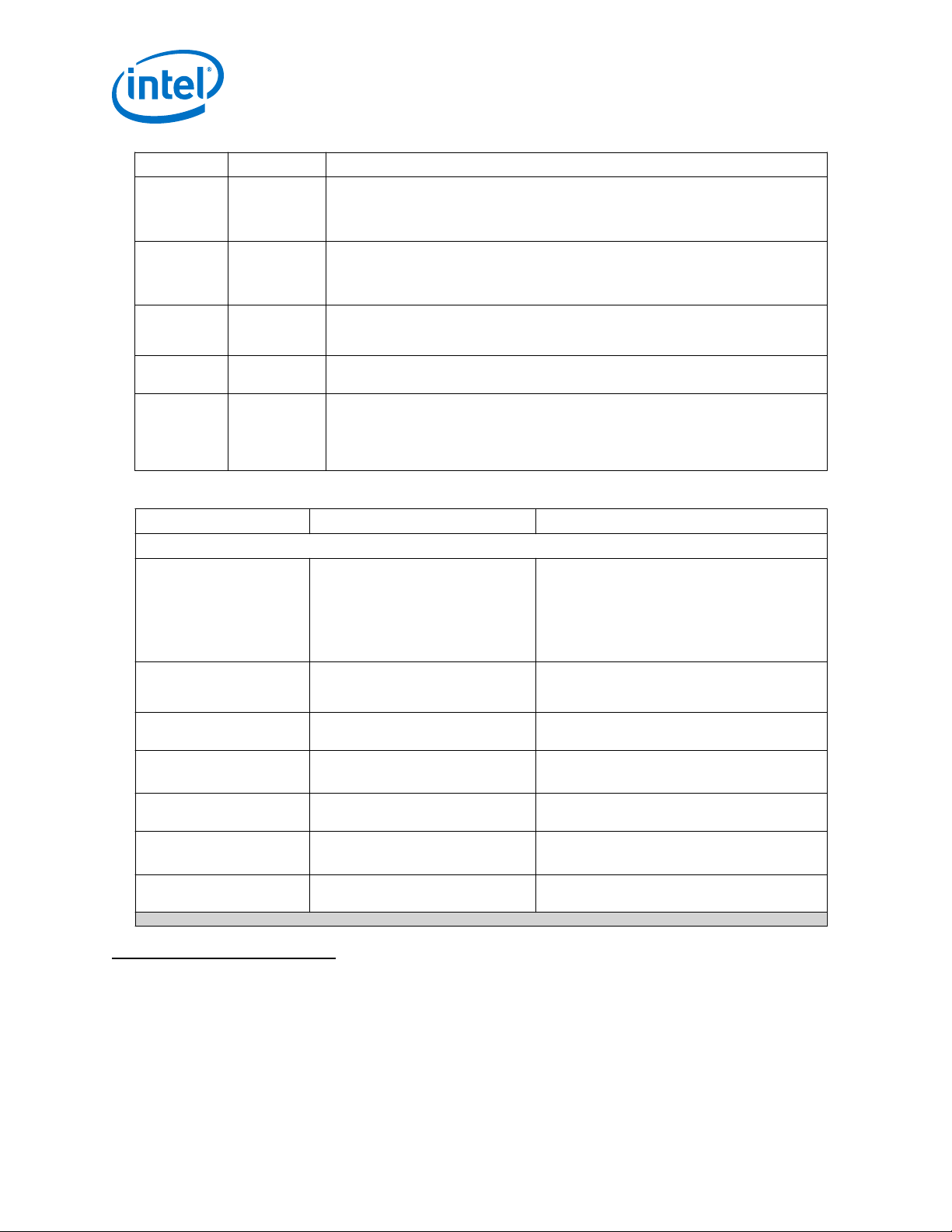
2. Implementing Protocols in Arria 10 Transceivers
UG-01143 | 2018.06.15
Parameter Value Description
Store
configuration
to selected
profile
Load
configuration
from selected
profile
Clear selected
profile
Clear all
profiles
Refresh
selected
profile
- Clicking this button saves or stores the current Native PHY parameter settings to the
profile specified by the Selected reconfiguration profile parameter.
- Clicking this button loads the current Native PHY with parameter settings from the
stored profile specified by the Selected reconfiguration profile parameter.
- Clicking this button clears or erases the stored Native PHY parameter settings for the
profile specified by the Selected reconfiguration profile parameter. An empty profile
defaults to the current parameter settings of the Native PHY.
- Clicking this button clears the Native PHY parameter settings for all the profiles.
- Clicking this button is equivalent to clicking the Load configuration from selected
profile and Store configuration to selected profile buttons in sequence. This
operation loads the Native PHY parameter settings from stored profile specified by the
Selected reconfiguration profile parameter and subsequently stores or saves the
parameters back to the profile.
Table 43. Analog PMA Settings (Optional) for Dynamic Reconfiguration
Parameter Value Description
TX Analog PMA Settings
Analog Mode (Load Intelrecommended Default
settings)
Override Intel-recommended
Analog Mode Default settings
Output Swing Level (VOD) 0-31 Selects the transmitter programmable output
Pre-Emphasis First Pre-Tap
Polarit
Pre-Emphasis First Pre-Tap
Magnitude
Pre-Emphasis Second PreTap Polarity
Pre-Emphasis Second PreTap Magnitude
Cei_11100_lr to xfp_9950 Selects the analog protocol mode to pre-select the
On/Off Enables the option to override the Intel-
Fir_pre_1t_neg
Fir_pre_1t_pos
(29)
0-16
Fir_pre_2t_neg
Fir_pre_2t_pos
(30)
0-7
TX pin swing settings (VOD, Pre-emphasis, and
Slew Rate). After loading the pre-selected values
in the GUI, if one or more of the individual TX pin
swing settings need to be changed, then enable
the option to override the Intel-recommended
defaults to individually modify the settings.
recommended settings for the selected TX Analog
Mode for one or more TX analog parameters.
differential voltage swing.
Selects the polarity of the first pre-tap for preemphasis.
Selects the magnitude of the first pre-tap for preemphasis
Selects the polarity of the second pre-tap for preemphasis.
Selects the magnitude of the second pre-tap for
pre-emphasis.
continued...
(29)
For more information refer to Available Options table in the
XCVR_A10_TX_PRE_EMP_SWITCHING_CTRL_PRE_TAP_1T section of the Analog Parameter
Settings chapter.
(30)
For more information refer to Available Options table in the
XCVR_A10_TX_PRE_EMP_SWITCHING_CTRL_PRE_TAP_2T section of the Analog Parameter
Settings chapter.
Intel® Arria® 10 Transceiver PHY User Guide
70
Page 71

2. Implementing Protocols in Arria 10 Transceivers
UG-01143 | 2018.06.15
Parameter Value Description
Pre-Emphasis First Post-Tap
Polarity
Pre-Emphasis First Post-Tap
Magnitude
Pre-Emphasis Second PostTap Polarity
Pre-Emphasis Second PostTap Magnitude
Slew Rate Control
High-Speed Compensation Enable/Disable Enables the power-distribution network (PDN)
On-Chip termination
Fir_post_1t_neg
Fir_post_1t_pos
(31)
0-25
Fir_post_2t_neg
Fir_post_2t_pos
(32)
0-12
slew_r0 to slew_r5
r_r1
Selects the polarity of the first post-tap for preemphasis
Selects the magnitude of the first post-tap for
pre-emphasis.
Selects the polarity of the second post-tap for
pre-emphasis.
Selects the magnitude of the second post-tap for
pre-emphasis
Selects the slew rate of the TX output signal. Valid
values span from slowest to the fastest rate.
induced inter-symbol interference (ISI)
compensation in the TX driver. When enabled, it
reduces the PDN induced ISI jitter, but increases
the power consumption.
Selects the on-chip TX differential termination.
r_r2
RX Analog PMA settings
Override Intel-recommended
Default settings
CTLE (Continuous Time
Linear Equalizer) mode
DC gain control of high gain
mode CTLE
AC Gain Control of High Gain
Mode CTLE
AC Gain Control of High Data
Rate Mode CTLE
Variable Gain Amplifier
(VGA) Voltage Swing Select
Decision Feedback Equalizer
(DFE) Fixed Tap 1 Coefficient
Decision Feedback Equalizer
(DFE) Fixed Tap 2 Coefficient
On/Off Enables the option to override the Intel-
non_s1_mode
S1_mode
No_dc_gain to stg4_gain7
radp_ctle_acgain_4s_0 to
radp_ctle_acgain_4s_28
radp_ctle_eqz_1s_sel_0 to
Radp_ctle_eqz_1s_sel_15
radp_vga_sel_0 to
radp_vga_sel_7
radp_dfe_fxtap1_0 to
radp_dfe_fxtap1_127
radp_dfe_fxtap2_0 to
radp_dfe_fxtap2_127
recommended settings for one or more RX analog
parameters
Selects between the RX high gain mode
non_s1_mode or RX high data rate mode
s1_mode for the Continuous Time Linear
Equalizer (CTLE).
Selects the DC gain of the Continuous Time Linear
Equalizer (CTLE) in high gain mode
Selects the AC gain of the Continuous Time Linear
Equalizer (CTLE) in high gain mode when CTLE is
in manual mode.
Selects the AC gain of the Continuous Time Linear
Equalizer (CTLE) in high data rate mode when
CTLE is in manual mode.
Selects the Variable Gain Amplifier (VGA) output
voltage swing when both the CTLE and DFE blocks
are in manual mode
Selects the co-efficient of the fixed tap 1 of the
Decision Feedback Equalizer (DFE) when
operating in manual mode
Selects the co-efficient of the fixed tap 2 of the
Decision Feedback Equalizer (DFE) when
operating in manual mode
continued...
(31)
For more information refer to Available Options table in the
XCVR_A10_TX_PRE_EMP_SWITCHING_CTRL_1ST_POST_TAP section of the Analog Parameter
Settings chapter.
(32)
For more information refer to Available Options table in the
XCVR_A10_TX_PRE_EMP_SWITCHING_CTRL_2ND_POST_TAP section of the Analog Parameter
Settings chapter.
Intel® Arria® 10 Transceiver PHY User Guide
71
Page 72

Parameter Value Description
Decision Feedback Equalizer
(DFE) Fixed Tap 3 Coefficient
Decision Feedback Equalizer
(DFE) Fixed Tap 4 Coefficient
Decision Feedback Equalizer
(DFE) Fixed Tap 5 Coefficient
radp_dfe_fxtap3_0 to
radp_dfe_fxtap3_127
radp_dfe_fxtap4_0 to
radp_dfe_fxtap4_63
radp_dfe_fxtap5_0 to
radp_dfe_fxtap5_63
2. Implementing Protocols in Arria 10 Transceivers
UG-01143 | 2018.06.15
Selects the co-efficient of the fixed tap 3 of the
Decision Feedback Equalizer (DFE) when
operating in manual mode.
Selects the co-efficient of the fixed tap 4 of the
Decision Feedback Equalizer (DFE) when
operating in manual mode.
Selects the co-efficient of the fixed tap 5 of the
Decision Feedback Equalizer (DFE) when
operating in manual mode.
Decision Feedback Equalizer
(DFE) Fixed Tap 6 Coefficient
Decision Feedback Equalizer
(DFE) Fixed Tap 7 Coefficient
Decision Feedback Equalizer
(DFE) Fixed Tap 8 Coefficient
Decision Feedback Equalizer
(DFE) Fixed Tap 9 Coefficient
Decision Feedback Equalizer
(DFE) Fixed Tap 10 Coefficient
Decision Feedback Equalizer
(DFE) Fixed Tap 11 Coefficient
On-Chip termination
radp_dfe_fxtap6_0 to
radp_dfe_fxtap6_31
radp_dfe_fxtap7_0 to
radp_dfe_fxtap7_31
radp_dfe_fxtap8_0 to
radp_dfe_fxtap8_31
radp_dfe_fxtap9_0 to
radp_dfe_fxtap9_31
radp_dfe_fxtap10_0 to
radp_dfe_fxtap10_31
radp_dfe_fxtap11_0 to
radp_dfe_fxtap11_31
R_ext0, r_r1, r_r2
Table 44. Generation Options
Parameter Value Description
Generate parameter
documentation file
On/Off When you turn on this option, generation produces a Comma-
Selects the co-efficient of the fixed tap 6 of the
Decision Feedback Equalizer (DFE) when
operating in manual mode.
Selects the co-efficient of the fixed tap 7 of the
Decision Feedback Equalizer (DFE) when
operating in manual mode.
Selects the co-efficient of the fixed tap 8 of the
Decision Feedback Equalizer (DFE) when
operating in manual mode.
Selects the co-efficient of the fixed tap 9 of the
Decision Feedback Equalizer (DFE) when
operating in manual mode.
Selects the co-efficient of the fixed tap 10 of the
Decision Feedback Equalizer (DFE) when
operating in manual mode.
Selects the co-efficient of the fixed tap 11 of the
Decision Feedback Equalizer (DFE) when
operating in manual mode.
Selects the on-chip RX differential termination.
Separated Value (.csv ) file with descriptions of the Transceiver
Native PHY IP parameters.
Related Information
• Analog Parameter Settings on page 585
• XCVR_A10_TX_PRE_EMP_SWITCHING_CTRL_PRE_TAP_1T on page 602
• XCVR_A10_TX_PRE_EMP_SWITCHING_CTRL_PRE_TAP_2T on page 602
• XCVR_A10_TX_PRE_EMP_SWITCHING_CTRL_1ST_POST_TAP on page 603
• XCVR_A10_TX_PRE_EMP_SWITCHING_CTRL_2ND_POST_TAP on page 604
• Reconfiguration Interface and Dynamic Reconfiguration on page 502
• Transmitter Pre-Emphasis First Pre-Tap Value on page 600
• Transmitter Pre-Emphasis Second Pre-Tap Value on page 600
• Transmitter Pre-Emphasis First Post-Tap Value on page 601
• Transmitter Pre-Emphasis Second Post-Tap Value on page 601
Intel® Arria® 10 Transceiver PHY User Guide
72
Page 73

2. Implementing Protocols in Arria 10 Transceivers
UG-01143 | 2018.06.15
2.4.8. PMA Ports
This section describes the PMA and calibration ports for the Arria 10 Transceiver Native
PHY IP core.
The following tables, the variables represent these parameters:
• <n>—The number of lanes
• <d>—The serialization factor
• <s>—The symbol size
• <p>—The number of PLLs
Table 45. TX PMA Ports
Name Direction Clock Domain Description
tx_serial_data[<n>
-1:0]
tx_serial_clk0
tx_bonding_clocks[
<n><6>-1:0]
tx_serial_clk1
tx_serial_clk2
tx_serial_clk3
tx_serial_clk4
tx_analog_reset_ac
k
tx_pma_clkout
tx_pma_div_clkout
tx_pma_iqtxrx_clko
ut
tx_pma_elecidle[<n
>-1:0]
Input N/A This is the serial data output of the TX PMA.
Input Clock This is the serial clock from the TX PLL. The frequency of this
Input Clock This is a 6-bit bus which carries the low speed parallel clock
Inputs Clocks These are the serial clocks from the TX PLL. The frequency of
Output Asynchronous
Output Clock This clock is the low speed parallel clock from the TX PMA. It
Output Clock
Output Clock This port is available if you turn on Enable tx_
Input Asynchronous When you assert this signal, the transmitter is forced to
clock depends on the data rate and clock division factor. This
clock is for non bonded channels only. For bonded channels
use the tx_bonding_clocks clock TX input.
per channel. These clocks are outputs from the master CGB.
Use these clocks for bonded channels only.
Optional Ports
these clocks depends on the data rate and clock division
factor. These additional ports are enabled when you specify
more than one TX PLL.
Enables the optional tx_pma_analog_reset_ack output.
This port should not be used for register mode data transfers
is available when you turn on Enable tx_pma_clkout port
in the Transceiver Native PHY IP core Parameter Editor.
If you specify a tx_pma_div_clkout division factor of 1 or
2, this clock output is derived from the PMA parallel clock
(low speed parallel clock). If you specify a
tx_pma_div_clkout division factor of 33, 40, or 66, this
clock is derived from the PMA serial clock. This clock is
commonly used when the interface to the TX FIFO runs at a
different rate than the PMA parallel clock frequency, such as
66:40 applications.
pma_iqtxrx_clkout port in the Transceiver Native PHY IP
core Parameter Editor. This output clock can be used to
cascade the TX PMA output clock to the input of a PLL.
electrical idle. This port has no effect when you configure the
transceiver for the PCI Express protocol.
(33)
continued...
(33)
This clock is not to be used to clock the FPGA - transceiver interface. This clock may be used
as a reference clock to an external clock cleaner.
Intel® Arria® 10 Transceiver PHY User Guide
73
Page 74

Name Direction Clock Domain Description
tx_pma_qpipullup[<
n>-1:0]
tx_pma_qpipulldn[<
n>-1:0]
tx_pma_txdetectrx[
<n>-1:0]
tx_pma_rxfound[<n>
-1:0]
rx_seriallpbken[<n
>-1:0]
2. Implementing Protocols in Arria 10 Transceivers
UG-01143 | 2018.06.15
Input Asynchronous This port is available if you turn on Enable
Input Asynchronous This port is available if you turn on Enable
Input Asynchronous This port is available if you turn on Enable
tx_pma_qpipullup port (QPI) in the Transceiver Native PHY
IP core Parameter Editor. It is only used for Quick Path
Interconnect (QPI) applications.
tx_pma_qpipulldn port (QPI) in the Transceiver Native PHY
IP core Parameter Editor. It is only used for Quick Path
Interconnect (QPI) applications.
tx_pma_txdetectrx port (QPI) in the Transceiver Native
PHY IP core Parameter Editor. When asserted, the receiver
detect block in TX PMA detects the presence of a receiver at
the other end of the channel. After receiving the
tx_pma_txdetectrx request, the receiver detect block
initiates the detection process. Use this port for Quick Path
Interconnect (QPI) applications only.
Output Synchronous to
rx_coreclkin or
rx_clkout based
on the
configuration.
Input Asynchronous This port is available if you turn on Enable rx_seriallpbken
This port is available if you turn on Enable
tx_rxfound_pma port (QPI) in the Transceiver Native PHY
IP core Parameter Editor. When asserted, indicates that
the receiver detect block in TX PMA has detected a receiver
at the other end of the channel. Use this port for Quick Path
Interconnect (QPI) applications only.
port in the Transceiver Native PHY IP core Parameter
Editor. The assertion of this signal enables the TX to RX
serial loopback path within the transceiver. This signal can be
enabled in Duplex or Simplex mode. If enabled in Simplex
mode, you must drive the signal on both the TX and RX
instances from the same source. Otherwise the design fails
compilation.
Table 46. RX PMA Ports
Name Direction Clock Domain Description
rx_serial_data[<n>
-1:0]
rx_cdr_refclk0
rx_cdr_refclk1–
rx_cdr_refclk4
rx_analog_reset_ac
k
rx_pma_clkout
rx_pma_div_clkout
Input N/A Specifies serial data input to the RX PMA.
Input Clock Specifies reference clock input to the RX clock data recovery
Input Clock Specifies reference clock inputs to the RX clock data recovery
Output Asynchronous Enables the optional rx_pma_analog_reset_ack output. This
Output Clock This clock is the recovered parallel clock from the RX CDR
Output Clock The deserializer generates this clock. This is used to drive core
(CDR) circuitry.
Optional Ports
(CDR) circuitry.
port should not be used for register mode data transfers.
circuitry.
logic, PCS-to-FPGA fabric interface, or both. If you specify a
rx_pma_div_clkout division factor of 1 or 2, this clock output
is derived from the PMA parallel clock (low speed parallel
clock). If you specify a rx_pma_div_clkout division factor of
33, 40, or 66, this clock is derived from the PMA serial clock.
This clock is commonly used when the interface to the RX FIFO
runs at a different rate than the PMA parallel clock (low speed
parallel clock) frequency, such as 66:40 applications.
continued...
Intel® Arria® 10 Transceiver PHY User Guide
74
Page 75
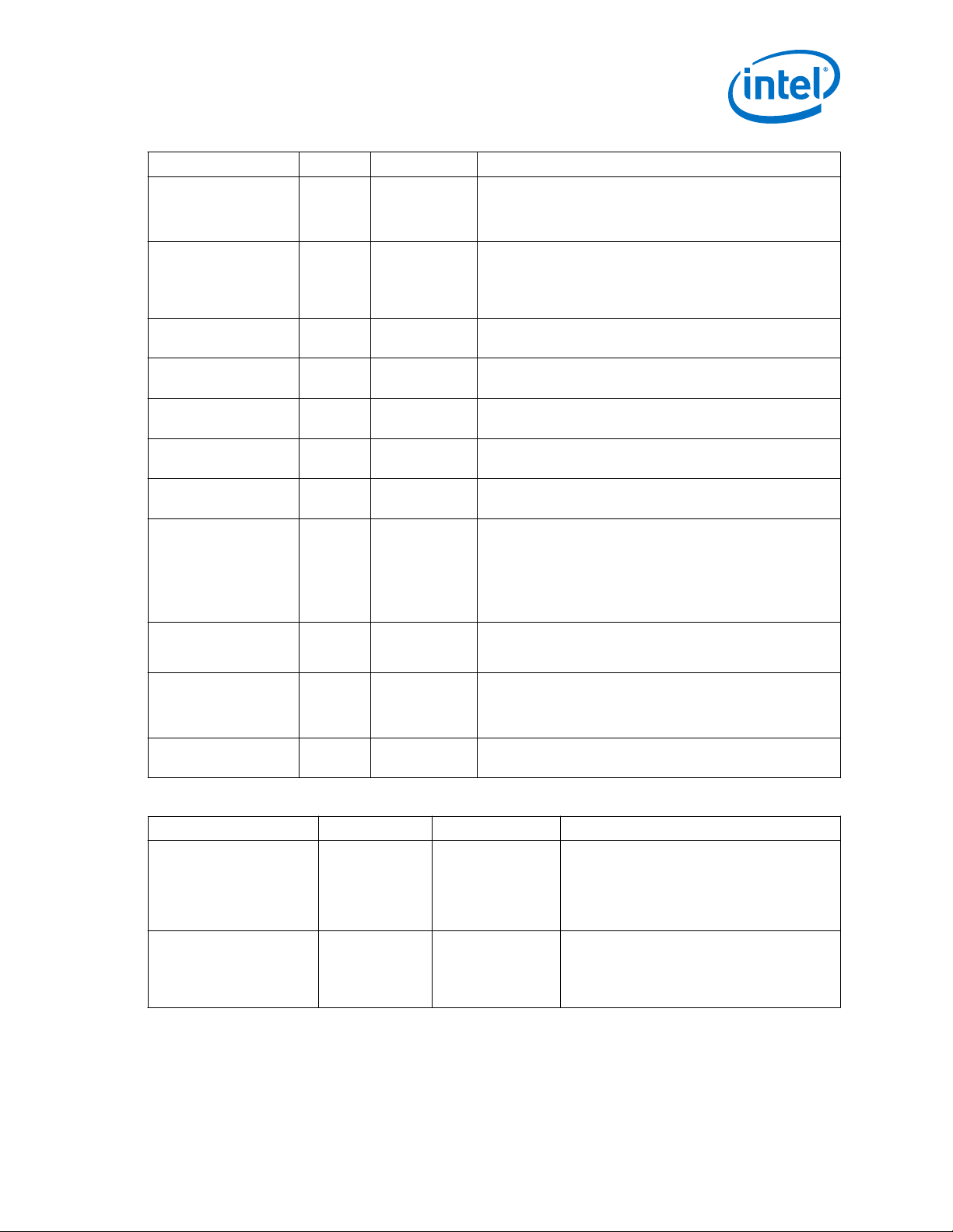
2. Implementing Protocols in Arria 10 Transceivers
UG-01143 | 2018.06.15
Name Direction Clock Domain Description
rx_pma_iqtxrx_clko
Output Clock This port is available if you turn on Enable rx_
ut
rx_pma_clkslip
rx_pma_qpipulldn[<
Output Clock When asserted, indicates that the deserializer has either
Input Asynchronous This port is only used for Quick Path Interconnect (QPI)
n>-1:0]
rx_is_lockedtodat
Output
rx_clkout
a[<n>-1:0]
rx_is_lockedtoref[
Output
rx_clkout
<n>-1:0]
rx_set_locktodata[
Input Asynchronous This port provides manual control of the RX CDR circuitry.
<n>-1:0]
rx_set_locktoref[<
Input Asynchronous This port provides manual control of the RX CDR circuitry.
n>-1:0]
rx_seriallpbken[<n
Input Asynchronous This port is available if you turn on Enable rx_ seriallpbken
>-1:0]
rx_prbs_done[<n>-1
:0]
rx_prbs_err[<n>-1:
0]
rx_prbs_err_clr[<n
>-1:0]
Output
Output
Input
rx_coreclkin
or rx_clkout
rx_coreclkin
or rx_clkout
rx_coreclkin
or rx_clkout
pma_iqtxrx_clkout port in the Transceiver Native PHY IP
core Parameter Editor. This output clock can be used to
cascade the RX PMA output clock to the input of a PLL.
skipped one serial bit or paused the serial clock for one cycle to
achieve word alignment. As a result, the period of the parallel
clock could be extended by 1 unit interval (UI) during the clock
slip operation.
applications.
When asserted, indicates that the CDR PLL is locked to the
incoming data, rx_serial_data.
When asserted, indicates that the CDR PLL is locked to the
input reference clock.
port in the Transceiver Native PHY IP core Parameter Editor.
The assertion of this signal enables the TX to RX serial
loopback path within the transceiver. This signal is enabled in
Duplex or Simplex mode. If enabled in Simplex mode, you
must drive the signal on both the TX and RX instances from
the same source. Otherwise the design fails compilation.
When asserted, indicates the verifier has aligned and captured
consecutive PRBS patterns and the first pass through a
polynomial is complete.
When asserted, indicates an error only after the
rx_prbs_done signal has been asserted. This signal gets
asserted for three parallel clock cycles for every error that
occurs. Errors can only occur once per word.
When asserted, clears the PRBS pattern and deasserts the
rx_prbs_done signal.
Table 47. Calibration Status Ports
Name Direction Clock Domain Description
tx_cal_busy[<n>-1:0]
rx_cal_busy[<n>-1:0]
Output Asynchronous When asserted, indicates that the initial TX
Output Asynchronous When asserted, indicates that the initial RX
calibration is in progress. For both initial and
manual recalibration, this signal is asserted
during calibration and deasserts after calibration
is completed. You must hold the channel in
reset until calibration completes.
calibration is in progress. For both initial and
manual recalibration, this signal is asserted
during calibration and deasserts after calibration
is completed.
Intel® Arria® 10 Transceiver PHY User Guide
75
Page 76

Table 48. Reset Ports
reconfig_reset
reconfig_clk
reconfig_avmm
TX Parallel Data, Control, Clocks
Enhanced PCS TX FIFO
Interlaken Frame Generator
Reconfiguration
Registers
TX Enhanced PCS
RX Enhanced PCS
Nios Hard
Calibration IP
TX PMA
Serializer
RX PMA
DeserializerCDR
tx_cal_busy
rx_cal_busy
Serial Data
Optional Ports
CDR Control
QPI
Serial Data
Clock
Generation
Block
tx_serial_clk0
(from TX PLL)
tx_analog_reset
RX Parallel Data, Control, Clocks
Enhanced PCS RX FIFO
Interlaken Frame Synchronizer
10GBASE-R BER Checker
Bitslip
Bitslip
rx_analog_reset
Clocks
PRBS
Optional Ports
Clocks
QPI
Arria 10 Transceiver Native PHY
Name Direction Clock Domain
tx_analogreset[<n>-1:
Input Asynchronous Resets the analog TX portion of the transceiver
0]
tx_digitalreset[<n>-1
Input Asynchronous Resets the digital TX portion of the transceiver
:0]
rx_analogreset[<n>-1:
Input Asynchronous Resets the analog RX portion of the transceiver
0]
rx_digitalreset[<n>-1
Input Asynchronous Resets the digital RX portion of the transceiver
:0]
2.4.9. Enhanced PCS Ports
Figure 24. Enhanced PCS Interfaces
The labeled inputs and outputs to the PMA and PCS modules represent buses, not individual signals.
2. Implementing Protocols in Arria 10 Transceivers
UG-01143 | 2018.06.15
(34)
PHY.
PHY.
PHY.
PHY.
Description
In the following tables, the variables represent these parameters:
• <n>—The number of lanes
• <d>—The serialization factor
• <s>— The symbol size
• <p>—The number of PLLs
(34)
Although the reset ports are not synchronous to any clock domain, Intel recommends that you
synchronize the reset ports with the system clock.
Intel® Arria® 10 Transceiver PHY User Guide
76
Page 77

2. Implementing Protocols in Arria 10 Transceivers
UG-01143 | 2018.06.15
Table 49. Enhanced TX PCS: Parallel Data, Control, and Clocks
Name Direction Clock Domain Description
tx_parallel_data[
<n>128-1:0]
unused_tx_paralle
l_data
tx_control[<n><3>
-1:0] or
tx_control[<n><18
>-1:0]
unused_tx_contro
l[<n> <15>-1:0]
tx_err_ins
Input Synchronous to
Input
Input Synchronous to
Input Synchronous to
Input
the clock driving
the write side of
the FIFO
(tx_coreclkin
or tx_clkout)
tx_clkout
the clock driving
the write side of
the FIFO
(tx_coreclkin
or tx_clkout)
the clock driving
the write side of
the FIFO
(tx_coreclkin
or tx_clkout)
tx_coreclkin
TX parallel data inputs from the FPGA fabric to the TX PCS. If
you select Enable simplified interface in the Transceiver
Native PHY IP Parameter Editor, tx_parallel_data
includes only the bits required for the configuration you specify.
You must ground the data pins that are not active. For single
width configuration, the following bits are active:
• 32-bit FPGA fabric to PCS interface width:
tx_parallel_data[31:0]. Ground [127:32].
• 40-bit FPGA fabric to PCS interface width:
tx_parallel_data[39:0]. Ground [127:40].
• 64-bit FPGA fabric to PCS interface width:
tx_parallel_data[63:0] Ground [127:64].
For double width configuration, the following bits are active:
• 40-bit FPGA fabric to PCS interface width: data[103:64],
[39:0]. Ground [127:104], [63:40].
• 64-bit FPGA fabric to PCS interface width: data[127:64],
[63:0].
Double-width mode is not supported for 32-bit, 50-bit, and 67bit FPGA fabric to PCS interface widths.
Port is enabled, when you enable Enable simplified data
interface. Connect all of these bits to 0. When Enable
simplified data interface is disabled, the unused bits are a
part of tx_parallel_data. Refer to tx_parallel_data to
identify the bits you need to ground.
tx_control bits have different functionality depending on the
transceiver configuration rule selected. When Simplified data
interface is enabled, the number of bits in this bus change
because the unused bits are shown as part of the
unused_tx_control port.
Refer to Enhanced PCS TX and RX Control Ports on page 83
section for more details.
This port is enabled when you enable Enable simplified data
interface. Connect all of these bits to 0. When Enable
simplified data interface is disabled, the unused bits are a
part of the tx_control.
Refer to tx_control to identify the bits you need to ground.
For the Interlaken protocol, you can use this bit to insert the
synchronous header and CRC32 errors if you have turned on
Enable simplified data interface.
When asserted, the synchronous header for that cycle word is
replaced with a corrupted one. A CRC32 error is also inserted if
Enable Interlaken TX CRC-32 generator error insertion is
turned on. The corrupted sync header is 2'b00 for a control
word, and 2'b11 for a data word. For CRC32 error insertion, the
word used for CRC calculation for that cycle is incorrectly
inverted, causing an incorrect CRC32 in the Diagnostic Word of
the Metaframe.
Note that a synchronous header error and a CRC32 error
cannot be created for the Framing Control Words because the
Frame Control Words are created in the frame generator
continued...
Intel® Arria® 10 Transceiver PHY User Guide
77
Page 78

2. Implementing Protocols in Arria 10 Transceivers
Name Direction Clock Domain Description
embedded in TX PCS. Both the synchronous header error and
the CRC32 errors are inserted if the CRC-32 error insertion
feature is enabled in the Transceiver Native PHY IP GUI.
tx_coreclkin
tx_clkout
Input Clock The FPGA fabric clock. Drives the write side of the TX FIFO. For
the Interlaken protocol, the frequency of this clock could be
from datarate/67 to datarate/32. Using frequency lower than
this range can cause the TX FIFO to underflow and result in
data corruption.
Output Clock This is a parallel clock generated by the local CGB for non
bonded configurations, and master CGB for bonded
configurations. This clocks the blocks of the TX Enhanced PCS.
The frequency of this clock is equal to the datarate divided by
PCS/PMA interface width.
Table 50. Enhanced RX PCS: Parallel Data, Control, and Clocks
Name Direction Clock Domain Description
rx_parallel_data[<n
>128-1:0]
unused_rx_parallel_
data
rx_control[<n>
<20>-1:0]
unused_rx_control[<
n>10-1:0]
Output Synchronous
to the clock
driving the
read side of
the FIFO
(rx_coreclk
in or
rx_clkout)
Output
Output Synchronous
rx_clkout
to the clock
driving the
read side of
the FIFO
(rx_coreclk
in or
rx_clkout)
Output Synchronous
to the clock
driving the
read side of
the FIFO
RX parallel data from the RX PCS to the FPGA fabric. If you
select, Enable simplified data interface in the Transceiver
Native PHY IP GUI, rx_parallel_data includes only the bits
required for the configuration you specify. Otherwise, this
interface is 128 bits wide.
When FPGA fabric to PCS interface width is 64 bits, the
following bits are active for interfaces less than 128 bits. You
can leave the unused bits floating or not connected.
• 32-bit FPGA fabric to PCS width: data[31:0].
• 40-bit FPGA fabric to PCS width: data[39:0].
• 64-bit FPGA fabric to PCS width: data[63:0].
When the FPGA fabric to PCS interface width is 128 bits, the
following bits are active:
• 40-bit FPGA fabric to PCS width: data[103:64], [39:0].
• 64-bit FPGA fabric to PCS width: data[127:0].
This signal specifies the unused data when you turn on Enable
simplified data interface. When simplified data interface is
not set, the unused bits are a part of rx_parallel_data.
You can leave the unused data outputs floating or not
connected.
Indicates whether the rx_parallel_data bus is control or
data.
Refer to the Enhanced PCS TX and RX Control Ports on page
83 section for more details.
These signals only exist when you turn on Enable simplified
data interface. When simplified data interface is not set, the
unused bits are a part of rx_control. These outputs can be
left floating.
UG-01143 | 2018.06.15
continued...
Intel® Arria® 10 Transceiver PHY User Guide
78
Page 79

2. Implementing Protocols in Arria 10 Transceivers
UG-01143 | 2018.06.15
Name Direction Clock Domain Description
(rx_coreclk
in or
rx_clkout)
rx_coreclkin
rx_clkout
Input Clock The FPGA fabric clock. Drives the read side of the RX FIFO. For
Output Clock The low speed parallel clock recovered by the transceiver RX
Table 51. Enhanced PCS TX FIFO
Name Direction Clock Domain Description
tx_enh_data_valid[<n>1:0]
tx_enh_fifo_full[<n>-1
:0]
tx_enh_fifo_pfull[<n>1:0]
tx_enh_fifo_empty[<n>1:0]
tx_enh_fifo_pempty[<n>
-1:0]
Input Synchronous to
the clock driving
the write side of
the FIFO
(tx_coreclkin
or tx_clkout)
Output Synchronous to
the clock driving
the write side of
the FIFO
(tx_coreclkin
or tx_clkout)
Output Synchronous to
the clock driving
the write side of
the FIFO
tx_coreclkin
or tx_clkout
Output Synchronous to
the clock driving
the write side of
the FIFO
tx_coreclkin
or tx_clkout
Output Synchronous to
the clock driving
the write side of
the FIFO
tx_coreclkin
or tx_clkout
Interlaken protocol, the frequency of this clock could be from
datarate/67 to datarate/32.
PMA, that clocks the blocks in the RX Enhanced PCS. The
frequency of this clock is equal to data rate divided by
PCS/PMA interface width.
Assertion of this signal indicates that the TX data is valid.
Connect this signal to 1'b1 for 10GBASE-R without 1588.
For 10GBASE-R with 1588, you must control this signal
based on the gearbox ratio. For Basic and Interlaken, you
need to control this port based on TX FIFO flags so that
the FIFO does not underflow or overflow.
Refer to Enhanced PCS FIFO Operation on page 297 for
more details.
Assertion of this signal indicates the TX FIFO is full.
Because the depth is always constant, you can ignore this
signal for the phase compensation mode.
Refer to Enhanced PCS FIFO Operation on page 297 for
more details.
This signal gets asserted when the TX FIFO reaches its
partially full threshold. Because the depth is always
constant, you can ignore this signal for the phase
compensation mode.
Refer to Enhanced PCS FIFO Operation on page 297 for
more details.
When asserted, indicates that the TX FIFO is empty. This
signal gets asserted for 2 to 3 clock cycles. Because the
depth is always constant, you can ignore this signal for
the phase compensation mode.
Refer to Enhanced PCS FIFO Operation on page 297 for
more details.
When asserted, indicates that the TX FIFO has reached its
specified partially empty threshold. When you turn this
option on, the Enhanced PCS enables the
tx_enh_fifo_pempty port, which is asynchronous. This
signal gets asserted for 2 to 3 clock cycles. Because the
depth is always constant, you can ignore this signal for
the phase compensation mode.
Refer to Enhanced PCS FIFO Operation on page 297 for
more details.
Table 52. Enhanced PCS RX FIFO
Name Direction Clock Domain Description
rx_enh_data_valid[<n>
-1:0]
Output Synchronous to
the clock driving
the read side of
When asserted, indicates that rx_parallel_data is
valid. Discard invalid RX parallel data
whenrx_enh_data_valid signal is low.
continued...
Intel® Arria® 10 Transceiver PHY User Guide
79
Page 80

Name Direction Clock Domain Description
rx_enh_fifo_full[<n>1:0]
rx_enh_fifo_pfull[<n>
-1:0]
rx_enh_fifo_empty[<n>
-1:0]
rx_enh_fifo_pempty[<n
>-1:0]
rx_enh_fifo_del[<n>-1
:0]
rx_enh_fifo_insert[<n
>-1:0]
rx_enh_fifo_rd_en[<n>
-1:0]
rx_enh_fifo_align_va
l[<n>-1:0]
the FIFO
rx_coreclkin
or rx_clkout
Output Synchronous to
the clock driving
the read side of
the FIFO
rx_coreclkin
or rx_clkout
Output Synchronous to
the clock driving
the read side of
the FIFO
rx_coreclkin
or rx_clkout
Output Synchronous to
the clock driving
the read side of
the FIFO
rx_coreclkin
or rx_clkout
Output Synchronous to
the clock driving
the read side of
the FIFO
rx_coreclkin
or rx_clkout
Output Synchronous to
the clock driving
the read side of
the FIFO
rx_coreclkin
or rx_clkout
Output Synchronous to
the clock driving
the read side of
the FIFO
rx_coreclkin
or rx_clkout
Output Synchronous to
the clock driving
the read side of
the FIFO
rx_coreclkin
or rx_clkout
Input Synchronous to
the clock driving
the read side of
2. Implementing Protocols in Arria 10 Transceivers
UG-01143 | 2018.06.15
This option is available when you select the following
parameters:
• Enhanced PCS Transceiver configuration rules
specifies Interlaken
• Enhanced PCS Transceiver configuration rules
specifies Basic, and RX FIFO mode is Phase
compensation
• Enhanced PCS Transceiver configuration rules
specifies Basic, and RX FIFO mode is Register
Refer to Enhanced PCS FIFO Operation on page 297
for more details.
When asserted, indicates that the RX FIFO is full. This
signal gets asserted for 2 to 3 clock cycles.Because
the depth is always constant, you can ignore this
signal for the phase compensation mode.
Refer to Enhanced PCS FIFO Operation on page 297
for more details.
When asserted, indicates that the RX FIFO has
reached its specified partially full threshold. This signal
gets asserted for 2 to 3 clock cycles. Because the
depth is always constant, you can ignore this signal
for the phase compensation mode.
Refer to Enhanced PCS FIFO Operation on page 297
for more details.
When asserted, indicates that the RX FIFO is empty.
Because the depth is always constant, you can ignore
this signal for the phase compensation mode.
Refer to Enhanced PCS FIFO Operation on page 297
for more details.
When asserted, indicates that the RX FIFO has
reached its specified partially empty threshold.
Because the depth is always constant, you can ignore
this signal for the phase compensation mode.
Refer to Enhanced PCS FIFO Operation on page 297
for more details.
When asserted, indicates that a word has been deleted
from the RX FIFO. This signal gets asserted for 2 to 3
clock cycles. This signal is used for the 10GBASE-R
protocol.
When asserted, indicates that a word has been
inserted into the RX FIFO. This signal is used for the
10GBASE-R protocol.
For Interlaken only, when this signal is asserted, a
word is read form the RX FIFO. You need to control
this signal based on RX FIFO flags so that the FIFO
does not underflow or overflow.
When asserted, indicates that the word alignment
pattern has been found. This signal is only valid for
the Interlaken protocol.
continued...
Intel® Arria® 10 Transceiver PHY User Guide
80
Page 81
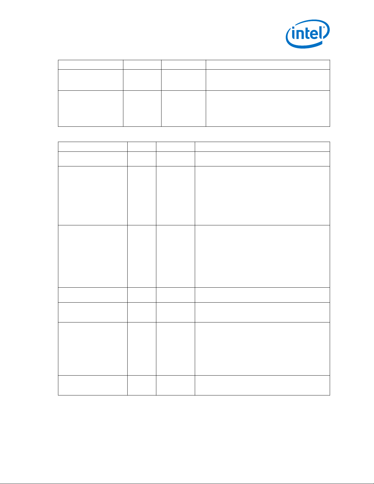
2. Implementing Protocols in Arria 10 Transceivers
UG-01143 | 2018.06.15
Name Direction Clock Domain Description
the FIFO
rx_coreclkin
or rx_clkout
rx_enh_fifo_align_cl
r[<n>-1:0]
Input Synchronous to
the clock driving
the read side of
the FIFO
When asserted, the FIFO resets and begins searching
for a new alignment pattern. This signal is only valid
for the Interlaken protocol. Assert this signal for at
least 4 cycles.
rx_coreclkin
or rx_clkout
Table 53. Interlaken Frame Generator, Synchronizer, and CRC32
Name Direction Clock Domain Description
tx_enh_frame[<n>-1:0]
tx_enh_frame_diag_stat
us[<n> 2-1:0]
tx_enh_frame_burst_en[
<n>-1:0]
rx_enh_frame[<n>-1:0]
rx_enh_frame_lock[<n>1:0]
rx_enh_frame_diag_stat
us[2 <n>-1:0]
rx_enh_crc32_err[<n>-1
:0]
Output
Input
Input
Output
Output
Output
Output
tx_clkout
tx_clkout
tx_clkout
rx_clkout
rx_clkout
rx_clkout
rx_clkout
Asserted for 2 or 3 parallel clock cycles to indicate the
beginning of a new metaframe.
Drives the lane status message contained in the framing
layer diagnostic word (bits[33:32]). This message is
inserted into the next diagnostic word generated by the
frame generator block. This bus must be held constant for 5
clock cycles before and after the tx_enh_frame pulse. The
following encodings are defined:
• Bit[1]: When 1, indicates the lane is operational. When
0, indicates the lane is not operational.
• Bit[0]: When 1, indicates the link is operational. When
0, indicates the link is not operational.
If Enable frame burst is enabled, this port controls frame
generator data reads from the TX FIFO to the frame
generator. It is latched once at the beginning of each
Metaframe. If the value of tx_enh_frame_burst_en is 0,
the frame generator does not read data from the TX FIFO
for current Metaframe. Instead, the frame generator inserts
SKIP words as the payload of Metaframe. When
tx_enh_frame_burst_en is 1, the frame generator reads
data from the TX FIFO for the current Metaframe. This port
must be held constant for 5 clock cycles before and after
the tx_enh_frame pulse.
When asserted, indicates the beginning of a new received
Metaframe. This signal is pulse stretched.
When asserted, indicates the Frame Synchronizer state
machine has achieved Metaframe delineation. This signal is
pulse stretched.
Drives the lane status message contained in the framing
layer diagnostic word (bits[33:32]). This signal is latched
when a valid diagnostic word is received in the end of the
Metaframe while the frame is locked. The following
encodings are defined:
• Bit[1]: When 1, indicates the lane is operational. When
0, indicates the lane is not operational.
• Bit[0]: When 1, indicates the link is operational. When
0, indicates the link is not operational.
When asserted, indicates a CRC error in the current
Metaframe. Asserted at the end of current Metaframe. This
signal gets asserted for 2 or 3 cycles.
Intel® Arria® 10 Transceiver PHY User Guide
81
Page 82

Table 54. 10GBASE-R BER Checker
Name Direction Clock Domain Description
rx_enh_highber[<n>-1:0
Output
rx_clkout
]
rx_enh_highber_clr_cn
Input
rx_clkout
t[<n>-1:0]
rx_enh_clr_errblk_coun
Input
rx_clkout
t[<n>-1:0] (10GBASE-R
and FEC)
Table 55. Block Synchronizer
Name Direction Clock Domain Description
rx_enh_blk_lock<n>-1:0
]
Output
rx_clkout
2. Implementing Protocols in Arria 10 Transceivers
UG-01143 | 2018.06.15
When asserted, indicates a bit error rate that is greater
than 10 -4. For the 10GBASE-R protocol, this BER rate
occurs when there are at least 16 errors within 125 µs.
This signal gets asserted for 2 to 3 clock cycles.
When asserted, clears the internal counter that indicates
the number of times the BER state machine has entered
the BER_BAD_SH state.
When asserted the error block counter resets to 0.
Assertion of this signal clears the internal counter that
counts the number of times the RX state machine has
entered the RX_E state. In modes where the FEC block is
enabled, the assertion of this signal resets the status
counters within the RX FEC block.
When asserted, indicates that block synchronizer has
achieved block delineation. This signal is used for
10GBASE-R and Interlaken.
Table 56. Gearbox
Name Direction Clock Domain Description
rx_bitslip[<n>-1:0]
tx_enh_bitslip[<n>-1:0
]
Table 57. KR-FEC
Name Direction Clock Domain Description
tx_enh_frame[<n>-1:0]
rx_enh_frame[<n>-1:0]
rx_enh_frame_diag_stat
us
Related Information
• ATX PLL IP Core on page 354
• CMU PLL IP Core on page 370
• fPLL IP Core on page 362
• Ports and Parameters on page 535
Input
Input
Output
Output
Output
rx_clkout The rx_parallel_data slips 1 bit for every positive edge
of the rx_bitslip input. Keep the minimum interval
between rx_bitslip pulses to at least 20 cycles. The
maximum shift is < pcswidth -1> bits, so that if the PCS is
64 bits wide, you can shift 0-63 bits.
rx_clkout
tx_clkout
rx_clkout
rx_clkout
The value of this signal controls the number of bits to slip
the tx_parallel_data before passing to the PMA.
Asynchronous status flag output of TX KR-FEC that signifies
the beginning of generated KR FEC frame
Asynchronous status flag output of RX KR-FEC that
signifies the beginning of received KR FEC frame
Asynchronous status flag output of RX KR-FEC that
indicates the status of the current received frame.
• 00: No error
• 01: Correctable Error
• 10: Un-correctale error
• 11: Reset condition/pre-lock condition
Intel® Arria® 10 Transceiver PHY User Guide
82
Page 83
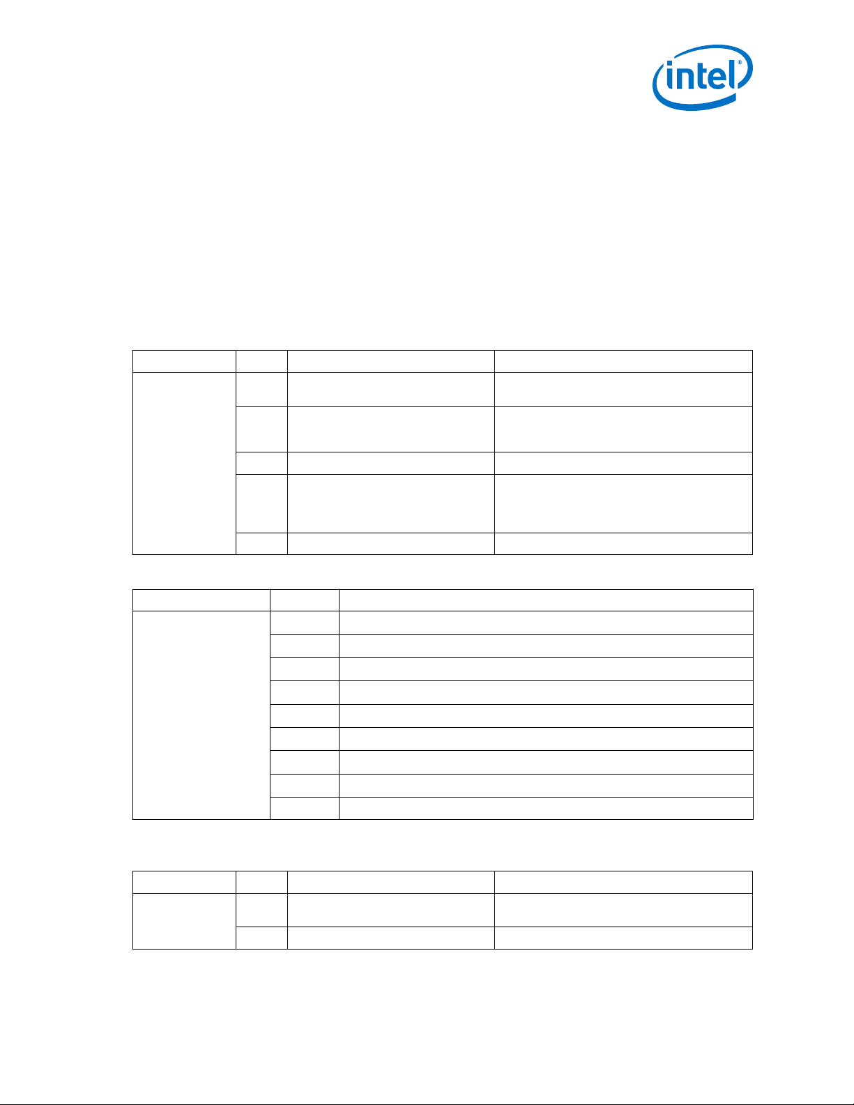
2. Implementing Protocols in Arria 10 Transceivers
UG-01143 | 2018.06.15
• Transceiver PHY Reset Controller Interfaces on page 437
2.4.9.1. Enhanced PCS TX and RX Control Ports
This section describes the tx_control and rx_control bit encodings for different
protocol configurations.
When Enable simplified data interface is ON, all of the unused ports shown in the
tables below, appear as a separate port. For example: It appears as
unused_tx_control/ unused_rx_control port.
Enhanced PCS TX Control Port Bit Encodings
Table 58. Bit Encodings for Interlaken
Name Bit Functionality Description
tx_control
[1:0] Synchronous header The value 2'b01 indicates a data word. The value
[2] Inversion control A logic low indicates that the built-in disparity
[7:3] Unused
[8] Insert synchronous header error or
CRC32
[17:9] Unused
2'b10 indicates a control word.
generator block in the Enhanced PCS maintains
the Interlaken running disparity.
You can use this bit to insert synchronous header
error or CRC32 errors. The functionality is similar
to tx_err_ins. Refer to tx_err_ins signal
description for more details.
Table 59. Bit Encodings for 10GBASE-R , 10GBASE-KR with FEC
Name Bit Functionality
tx_control
[0]
[1]
[2]
[3]
[4]
[5]
[6]
[7]
[17:8] Unused
XGMII control signal for parallel_data[7:0]
XGMII control signal for parallel_data[15:8]
XGMII control signal for parallel_data[23:16]
XGMII control signal for parallel_data[31:24]
XGMII control signal for parallel_data[39:32]
XGMII control signal for parallel_data[47:40]
XGMII control signal for parallel_data[55:48]
XGMII control signal for parallel_data[63:56]
Table 60. Bit Encodings for Basic Single Width Mode
For basic single width mode, the total word length is 66-bit with 64-bit data and 2-bit synchronous header.
Name
tx_control
Bit Functionality Description
[1:0] Synchronous header The value 2'b01 indicates a data word. The value
2'b10 indicates a control word.
[17:2] Unused
Intel® Arria® 10 Transceiver PHY User Guide
83
Page 84

2. Implementing Protocols in Arria 10 Transceivers
Table 61. Bit Encodings for Basic Double Width Mode
For basic double width mode, the total word length is 66-bit with 128-bit data and 4-bit synchronous header.
Name Bit Functionality Description
tx_control
[1:0] Synchronous header The value 2'b01 indicates a data word. The value
[8:2] Unused
[10:9] Synchronous header The value 2'b01 indicates a data word. The value
[17:11] Unused
Table 62. Bit Encodings for Basic Mode
In this case, the total word length is 67-bit with 64-bit data and 2-bit synchronous header.
Name Bit Functionality Description
tx_control
[1:0] Synchronous header The value 2'b01 indicates a data word. The value
[2] Inversion control A logic low indicates that built-in disparity
UG-01143 | 2018.06.15
2'b10 indicates a control word.
2'b10 indicates a control word.
2'b10 indicates a control word.
generator block in the Enhanced PCS maintains
the running disparity.
Enhanced PCS RX Control Port Bit Encodings
Table 63. Bit Encodings for Interlaken
Name Bit Functionality Description
rx_control
[1:0] Synchronous header The value 2'b01 indicates a data
[2] Inversion control A logic low indicates that the built-
[3] Payload word location A logic high (1'b1) indicates the
[4] Synchronization word location A logic high (1'b1) indicates the
[5] Scrambler state word location A logic high (1'b1) indicates the
[6] SKIP word location A logic high (1'b1) indicates the
[7] Diagnostic word location A logic high (1'b1) indicates the
word. The value 2'b10 indicates a
control word.
in disparity generator block in the
Enhanced PCS maintains the
Interlaken running disparity. In the
current implementation, this bit is
always tied logic low (1'b0).
payload word location in a
metaframe.
synchronization word location in a
metaframe.
scrambler word location in a
metaframe.
SKIP word location in a metaframe.
diagnostic word location in a
metaframe.
continued...
Intel® Arria® 10 Transceiver PHY User Guide
84
Page 85

2. Implementing Protocols in Arria 10 Transceivers
UG-01143 | 2018.06.15
Name Bit Functionality Description
[8] Synchronization header error, metaframe error,
[9] Block lock and frame lock status A logic high (1'b1) indicates that
[19:10] Unused
or CRC32 error status
Table 64. Bit Encodings for 10GBASE-R , 10GBASE-KR with FEC
Name Bit Functionality
rx_control
[0]
[1]
[2]
[3]
[4]
[5]
[6]
[7]
[19:8] Unused
XGMII control signal for parallel_data[7:0]
XGMII control signal for parallel_data[15:8]
XGMII control signal for parallel_data[23:16]
XGMII control signal for parallel_data[31:24]
XGMII control signal for parallel_data[39:32]
XGMII control signal for parallel_data[47:40]
XGMII control signal for parallel_data[55:48]
XGMII control signal for parallel_data[63:56]
A logic high (1'b1) indicates
synchronization header error,
metaframe error, or CRC32 error
status.
block lock and frame lock have
been achieved.
Table 65. Bit Encodings for Basic Single Width Mode
For basic single width mode, the total word length is 66-bit with 64-bit data and 2-bit synchronous header.
Name
rx_control
Bit Functionality Description
[1:0] Synchronous header The value 2'b01 indicates a data word. The value
[7:2] Unused
[9:8] Synchronous header error status The value 2'b01 indicates a data word. The value
[19:10] Unused
Table 66. Bit Encodings for Basic Double Width Mode
For basic double width mode, total word length is 66-bit with 128-bit data, and 4-bit synchronous header.
Name
rx_control
Bit Functionality Description
[1:0] Synchronous header The value 2'b01 indicates a data word. The
[7:2] Unused
[8] Synchronous header error status Active-high status signal that indicates a
[9] Block lock is achieved Active-high status signal indicating when block
[11:10] Synchronous header The value 2'b01 indicates a data word. The
2'b10 indicates a control word.
2'b10 indicates a control word.
value 2'b10 indicates a control word.
synchronous header error.
lock is achieved.
value 2'b10 indicates a control word.
continued...
Intel® Arria® 10 Transceiver PHY User Guide
85
Page 86
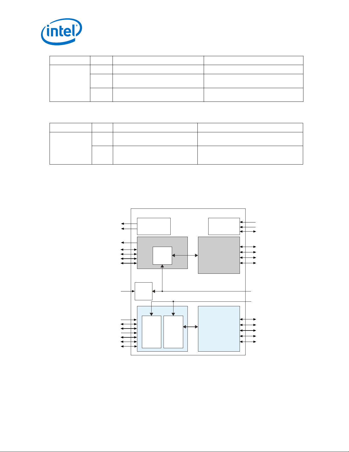
reconfig_reset
reconfig_clk
reconfig_avmm
Parallel Data, Control, Clocks
TX FIFO
8B/10B Encoder/Decoder
Reconfiguration
Registers
TX Standard PCS
RX Standard PCS
Nios Hard
Calibration IP
TX PMA
Serializer
RX PMA
DeserializerCDR
tx_cal_busy
rx_cal_busy
Serial Data
Optional Ports
CDR Control
QPI
PCIe
Serial Data
Clock
Generation
Block
tx_serial_clk0
(from TX PLL)
tx_analog_reset
Parallel Data, Control, Clocks
RX FIFO
Rate Match FIFO
Word Aligner & Bitslip
PCIe
rx_analog_reset
Clocks
PRBS
Bit & Byte Reversal
Polarity Inversion
PCIe
Optional Ports
Clocks
QPI
Arria 10 Transceiver Native PHY
2. Implementing Protocols in Arria 10 Transceivers
Name Bit Functionality Description
[17:12] Unused
[18] Synchronous header error status Active-high status signal that indicates a
[19] Block lock is achieved Active-high status signal indicating when Block
synchronous header error.
Lock is achieved.
Table 67. Bit Encodings for Basic Mode
In this case, the total word length is 67-bit with 64-bit data and 2-bit synchronous header.
Name Bit Functionality Description
rx_control
[1:0] Synchronous header The value 2'b01 indicates a data word. The value
2'b10 indicates a control word.
[2] Inversion control A logic low indicates that built-in disparity
generator block in the Enhanced PCS maintains
the running disparity.
2.4.10. Standard PCS Ports
Figure 25. Transceiver Channel using the Standard PCS Ports
Standard PCS ports appear if either one of the transceiver configuration modes is selected that uses Standard
PCS or if Data Path Reconfiguration is selected even if the transceiver configuration is not one of those that
uses Standard PCS.
UG-01143 | 2018.06.15
Intel® Arria® 10 Transceiver PHY User Guide
86
Page 87

2. Implementing Protocols in Arria 10 Transceivers
UG-01143 | 2018.06.15
In the following tables, the variables represent these parameters:
• <n>—The number of lanes
• <w>—The width of the interface
• <d>—The serialization factor
• <s>— The symbol size
• <p>—The number of PLLs
Table 68. TX Standard PCS: Data, Control, and Clocks
Name Direction Clock Domain Description
tx_parallel_data[<n>
128-1:0]
unused_tx_parallel_d
ata
tx_coreclkin
tx_clkout
Input
Input
Input Clock The FPGA fabric clock. This clock drives the write port of the
Output Clock This is the parallel clock generated by the local CGB for non
tx_clkout
tx_clkout
TX parallel data input from the FPGA fabric to the TX PCS.
This signal specifies the unused data when you turn on
Enable simplified data interface. When simplified data
interface is not set, the unused bits are a part of
tx_parallel_data. Connect all these bits to 0. If you do
not connect the unused data bits to 0, then TX parallel data
may not be serialized correctly by the Native PHY IP core.
TX FIFO.
bonded configurations, and master CGB for bonded
configuration. This clocks the tx_parallel_data from the
FPGA fabric to the TX PCS.
Table 69. RX Standard PCS: Data, Control, Status, and Clocks
Name Direction Clock Domain Description
rx_parallel_data[<n>
128-1:0]
unused_rx_parallel_da
ta
rx_clkout
rx_coreclkin
Output Synchronous
to the clock
driving the
read side of
the FIFO
(rx_coreclk
in or
rx_clkout)
Output Synchronous
to the clock
driving the
read side of
the FIFO
(rx_coreclk
in or
rx_clkout)
Output Clock The low speed parallel clock recovered by the transceiver RX
Input Clock RX parallel clock that drives the read side clock of the RX
RX parallel data from the RX PCS to the FPGA fabric. For
each 128-bit word of rx_parallel_data, the data bits
correspond to rx_parallel_data[7:0] when 8B/10B
decoder is enabled and rx_parallel_data[9:0] when
8B/10B decoder is disabled.
This signal specifies the unused data when you turn on
Enable simplified data interface. When simplified data
interface is not set, the unused bits are a part of
rx_parallel_data. These outputs can be left floating.
PMA, that clocks the blocks in the RX Standard PCS.
FIFO.
Intel® Arria® 10 Transceiver PHY User Guide
87
Page 88

Table 70. Standard PCS FIFO
Name Direction Clock Domain Description
tx_std_pcfifo_full[<n
>-1:0]
tx_std_pcfifo_empty[<
n>-1:0]
rx_std_pcfifo_full[<n
>-1:0]
rx_std_pcfifo_empty[<
n>-1:0]
Output Synchronous
Output Synchronous
Output Synchronous
Output Synchronous
2. Implementing Protocols in Arria 10 Transceivers
UG-01143 | 2018.06.15
Indicates when the standard TX FIFO is full.
to the clock
driving the
write side of
the FIFO
(tx_coreclki
n or
tx_clkout)
Indicates when the standard TX FIFO is empty.
to the clock
driving the
write side of
the FIFO
(tx_coreclki
n or
tx_clkout)
Indicates when the standard RX FIFO is full.
to the clock
driving the
read side of
the FIFO
(rx_coreclki
n or
rx_clkout)
Indicates when the standard RX FIFO is empty.
to the clock
driving the
read side of
the FIFO
(rx_coreclki
n or
rx_clkout)
Table 71. Rate Match FIFO
Name Direction Clock Domain Description
rx_std_rmfifo_full[<n
>-1:0]
rx_std_rmfifo_empty[<
n>-1:0]
rx_rmfifostatus[<n>-1
:0]
Output Asynchronous Rate match FIFO full flag. When asserted the rate match
Output Asynchronous Rate match FIFO empty flag. When asserted, match FIFO is
Output Asynchronous Indicates FIFO status. The following encodings are defined:
FIFO is full. You must synchronize this signal. This port is
only used for GigE mode.
empty. You must synchronize this signal. This port is only
used for GigE mode.
• 2'b00: Normal operation
•
2'b01: Deletion, rx_std_rmfifo_full = 1
•
2'b10: Insertion, rx_std_rmfifo_empty = 1
•
2'b11: Full. rx_rmfifostatus is a part of
rx_parallel_data. rx_rmfifostatus corresponds
to rx_parallel_data[14:13].
Intel® Arria® 10 Transceiver PHY User Guide
88
Page 89

2. Implementing Protocols in Arria 10 Transceivers
UG-01143 | 2018.06.15
Table 72. 8B/10B Encoder and Decoder
Name Direction Clock Domain Description
tx_datak
tx_forcedisp[<n>(<w>/
<s>-1:0]
tx_dispval[<n>(<w>/
<s>-1:0]
rx_datak[<n><w>/
<s>-1:0]
rx_errdetect[<n><w>/
<s>-1:0]
rx_disperr[<n><w>/
<s>-1:0]
rx_runningdisp[<n><w>
/<s>-1:0]
rx_patterndetect[<n><
w>/<s>-1:0]
Input tx_clkout
Input Asynchronous This signal allows you to force the disparity of the 8B/10B
Input Asynchronous Specifies the disparity of the data. When 0, indicates positive
Output
Output Synchronous to
rx_clkout rx_datak is exposed if 8B/10B is enabled and simplified
the clock
driving the
read side of the
FIFO
(rx_coreclki
n or
rx_clkout)
Output Synchronous to
the clock
driving the
read side of the
FIFO
(rx_coreclki
n or
rx_clkout)
Output Synchronous to
the clock
driving the
read side of the
FIFO
(rx_coreclki
n or
rx_clkout)
Output Asynchronous When asserted, indicates that the programmed word
tx_datak is exposed if 8B/10B enabled and simplified data
interface is set.When 1, indicates that the 8B/10B encoded
word of tx_parallel_data is control. When 0, indicates that
the 8B/10B encoded word of tx_parallel_data is data.
tx_datak is a part of tx_parallel_data when simplified
data interface is not set.
encoder. When "1", forces the disparity of the output data to
the value driven on tx_dispval. When "0", the current
running disparity continues. tx_forcedisp is a part of
tx_parallel_data. tx_forcedisp corresponds to
tx_parallel_data[9].
disparity, and when 1, indicates negative disparity.
tx_dispval is a part of tx_parallel_data. tx_dispval
corresponds to tx_dispval[10].
data interface is set. When 1, indicates that the 8B/10B
decoded word of rx_parallel_data is control. When 0,
indicates that the 8B/10B decoded word of
rx_parallel_data is data. rx_datak is a part of
rx_parallel_data when simplified data interface is not
set.
When asserted, indicates a code group violation detected on
the received code group. Used along with rx_disperr
signal to differentiate between code group violation and
disparity errors. The following encodings are defined for
rx_errdetect/rx_disperr:
• 2'b00: no error
• 2'b10: code group violation
•
2'b11: disparity error. rx_errdetect is a part of
rx_parallel_data. For each 128-bit word,
rx_errdetect corresponds to
rx_parallel_data[9].
When asserted, indicates a disparity error on the received
code group. rx_disperr is a part of rx_parallel_data.
For each 128-bit word, rx_disperr corresponds to
rx_parallel_data[11].
When high, indicates that rx_parallel_data was received
with negative disparity. When low, indicates that
rx_parallel_data was received with positive disparity.
rx_runningdisp is a part of rx_parallel_data. For
each 128 bit word, rx_runningdisp corresponds to
rx_parallel_data[15].
alignment pattern has been detected in the current word
boundary. rx_patterndetect is a part of
continued...
Intel® Arria® 10 Transceiver PHY User Guide
89
Page 90
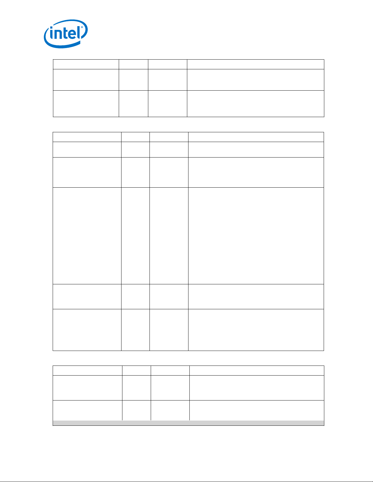
Name Direction Clock Domain Description
rx_syncstatus[<n><w>/
Output Asynchronous When asserted, indicates that the conditions required for
<s>-1:0]
Table 73. Word Aligner and Bitslip
Name Direction Clock Domain Description
tx_std_bitslipboundary
sel[5 <n>-1:0]
rx_std_bitslipboundary
sel[5 <n>-1:0]
rx_std_wa_patternalig
n[<n>-1:0]
rx_std_wa_a1a2size[<n>
-1:0]
rx_bitslip[<n>-1:0]
Input Asynchronous Bitslip boundary selection signal. Specifies the number of
Output Asynchronous This port is used in deterministic latency word aligner mode.
Input Synchronous
to rx_clkout
Input Asynchronous Used for the SONET protocol. Assert when the A1 and A2
Input Asynchronous Used when word aligner mode is bitslip mode. When the
2. Implementing Protocols in Arria 10 Transceivers
UG-01143 | 2018.06.15
rx_parallel_data. For each 128-bit word,
rx_patterndetect corresponds to
rx_parallel_data[12].
synchronization are being met. rx_syncstatus is a part of
rx_parallel_data. For each 128-bit word,
rx_syncstatus corresponds to rx_parallel_data[10].
bits that the TX bit slipper must slip.
This port reports the number of bits that the RX block
slipped. This port values should be taken into consideration
in either Deterministic Latency Mode or Manual Mode of
Word Aligner.
Active when you place the word aligner in manual mode. In
manual mode, you align words by asserting
rx_std_wa_patternalign. When the PCS-PMA Interface
width is 10 bits, rx_std_wa_patternalign is level
sensitive. For all the other PCS-PMA Interface widths,
rx_std_wa_patternalign is positive edge sensitive.
You can use this port only when the word aligner is
configured in manual or deterministic latency mode.
When the word aligner is in manual mode, and the PCS-PMA
interface width is 10 bits, this is a level sensitive signal. In
this case, the word aligner monitors the input data for the
word alignment pattern, and updates the word boundary
when it finds the alignment pattern.
For all other PCS-PMA interface widths, this signal is edge
sensitive.This signal is internally synchronized inside the
PCS using the PCS parallel clock and should be asserted for
at least 2 clock cycles to allow synchronization.
framing bytes must be detected. A1 and A2 are SONET
backplane bytes and are only used when the PMA data
width is 8 bits.
Word Aligner is in either Manual (PLD controlled),
Synchronous State Machine or Deterministic Latency ,the
rx_bitslip signal is not valid and should be tied to 0.
For every rising edge of the rx_std_bitslip signal, the
word boundary is shifted by 1 bit. Each bitslip removes the
earliest received bit from the received data.
Table 74. Bit Reversal and Polarity Inversion
Name Direction Clock Domain Description
rx_std_byterev_ena[<n>
-1:0]
rx_std_bitrev_ena[<n>1:0]
Intel® Arria® 10 Transceiver PHY User Guide
90
Input Asynchronous This control signal is available when the PMA width is 16 or
Input Asynchronous When asserted, enables bit reversal on the RX interface. Bit
20 bits. When asserted, enables byte reversal on the RX
interface. Used if the MSB and LSB of the transmitted data
are erroneously swapped.
order may be reversed if external transmission circuitry
transmits the most significant bit first. When enabled, the
continued...
Page 91
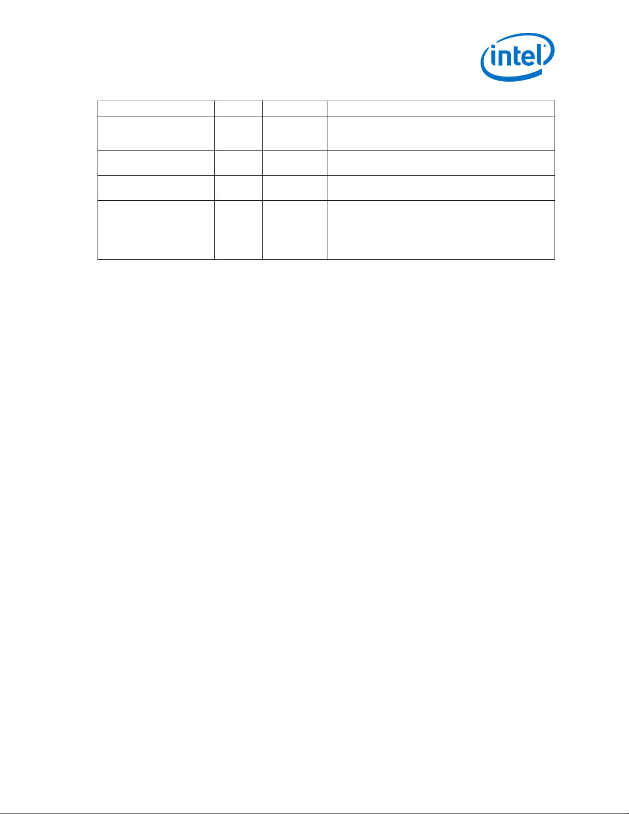
2. Implementing Protocols in Arria 10 Transceivers
UG-01143 | 2018.06.15
Name Direction Clock Domain Description
tx_polinv[<n>-1:0]
rx_polinv[<n>-1:0]
rx_std_signaldetect[<n
>-1:0]
Input Asynchronous When asserted, the TX polarity bit is inverted. Only active
Input Asynchronous When asserted, the RX polarity bit is inverted. Only active
Output Asynchronous When enabled, the signal threshold detection circuitry
Related Information
• ATX PLL IP Core on page 354
• CMU PLL IP Core on page 370
• fPLL IP Core on page 362
• Ports and Parameters on page 535
• Transceiver PHY Reset Controller Interfaces on page 437
• Analog Parameter Settings on page 585
receive circuitry receives all words in the reverse order. The
bit reversal circuitry operates on the output of the word
aligner.
when TX bit polarity inversion is enabled.
when RX bit polarity inversion is enabled.
senses whether the signal level present at the RX input
buffer is above the signal detect threshold voltage. You can
specify the signal detect threshold using a Quartus Prime
Settings File (.qsf) assignment. This signal is required for
the PCI Express, SATA and SAS protocols.
2.4.11. IP Core File Locations
When you generate your Transceiver Native PHY IP, the Quartus® Prime software
generates the HDL files that define your instance of the IP. In addition, the Quartus
Prime software generates an example Tcl script to compile and simulate your design in
the ModelSim* simulator. It also generates simulation scripts for Synopsys* VCS,
Aldec* Active-HDL, Aldec Riviera-Pro, and Cadence* Incisive Enterprise.
Intel® Arria® 10 Transceiver PHY User Guide
91
Page 92

Figure 26. Directory Structure for Generated Files
<Project Directory>
<your_ip_or_system_name>.qsys - Top-level IP variation file
<your_ip_or_system_name>.sopcinfo
<your_ip_name> - IP core variation files
<your_ip_name>.cmp - VHDL component declaration file
<your_ip_name>_bb - Verilog HDL black-box EDA synthesis file
<your_ip_name>_inst - IP instantiation template file
<your_ip_name>.ppf - XML I/O pin information file
<your_ip_name>.qip - Lists IP synthesis files
<your_ip_name>.sip - Lists files for simulation
<your_ip_name>.v or .vhd - Greybox timing netlist
synth - IP synthesis files
<your_ip_name>.v or .vhd - Top-level IP synthesis file
sim - IP simulation files
<your_ip_name>.v or .vhd - Top-level simulation file
aldec- Simulator setup scripts
<IP subcore> - IP subcore files
<HDL files>
sim
cadence - Simulator setup scripts
mentor - Simulator setup scripts
synopsys - Simulator setup scripts
<HDL files>
synth
2. Implementing Protocols in Arria 10 Transceivers
UG-01143 | 2018.06.15
Table 75. Transceiver Native PHY Files and Directories
<project_dir> The top-level project directory.
<your_ip_name> .v or .vhd The top-level design file.
<your_ip_name> .qip A list of all files necessary for Quartus Prime compilation.
The following table describes the directories and the most important files for the
parameterized Transceiver Native PHY IP core and the simulation environment. These
files are in clear text.
File Name Description
continued...
Intel® Arria® 10 Transceiver PHY User Guide
92
Page 93

2. Implementing Protocols in Arria 10 Transceivers
UG-01143 | 2018.06.15
File Name Description
<your_ip_name> .bsf A Block Symbol File (.bsf) for your Transceiver Native PHY
<project_dir>/<your_ip_name>/ The directory that stores the HDL files that define the
<project_dir>/sim The simulation directory.
<project_dir>/sim/aldec Simulation files for Riviera-PRO simulation tools.
<project_dir>/sim/cadence Simulation files for Cadence simulation tools.
<project_dir>/sim/mentor Simulation files for Mentor simulation tools.
<project_dir>/sim/synopsys Simulation files for Synopsys simulation tools.
<project_dir>/synth The directory that stores files used for synthesis.
instance.
Transceiver Native PHY IP.
The Verilog and VHDL Transceiver Native PHY IP cores have been tested with the
following simulators:
• ModelSim SE
• Synopsys VCS MX
• Cadence NCSim
If you select VHDL for your transceiver PHY, only the wrapper generated by the
Quartus Prime software is in VHDL. All the underlying files are written in Verilog or
SystemVerilog. To enable simulation using a VHDL-only ModelSim license, the
underlying Verilog and SystemVerilog files for the Transceiver Native PHY IP are
encrypted so that they can be used with the top-level VHDL wrapper without using a
mixed-language simulator.
For more information about simulating with ModelSim, refer to the Mentor Graphics
ModelSim and QuestaSim Support chapter in volume 3 of the Quartus Prime
Handbook.
The Transceiver Native PHY IP cores do not support the NativeLink feature in the
Quartus Prime software.
Related Information
• Simulating the Transceiver Native PHY IP Core on page 325
• Mentor Graphics ModelSim and QuestaSim Support
2.4.12. Unused Transceiver RX Channels
To prevent performance degradation of unused transceiver RX channels over time, the
following assignments must be added to an Arria 10 device QSF. You can either use a
global assignment or per-pin assignments.
set_global_assignment -name PRESERVE_UNUSED_XCVR_CHANNEL ON
or
set_instance_assignment -name PRESERVE_UNUSED_XCVR_CHANNEL ON -to
pin_name
Intel® Arria® 10 Transceiver PHY User Guide
93
Page 94

When you perform this procedure, the Intel Quartus Prime software instantiates the
clock data recovery (CDR) PLL corresponding to each unused receiver channel. The
CDR uses CLKUSR as reference clock and is configured to run at 1 Gbps. To use
CLKUSR as reference clock, the pin must be assigned a 100- to 125 MHz clock. When
you implement these assignments, it causes a power consumption increase per
receiver channel. Please contact your local support center for details.
Related Information
Unused/Idle Clock Line Requirements on page 389
2.4.13. Unsupported Features
Native PHY should not be included in QXP.
2.5. Interlaken
Interlaken is a scalable, channelized chip-to-chip interconnect protocol.
The key advantages of Interlaken are scalability and low I/O count compared to earlier
protocols such as SPI 4.2. Other key features include flow control, low overhead
framing, and extensive integrity checking. Interlaken operates on 64-bit data words
and 3 control bits, which are striped round-robin across the lanes. The protocol
accepts packets on 256 logical channels and is expandable to accommodate up to
65,536 logical channels. Packets are split into small bursts that can optionally be
interleaved. The burst semantics include integrity checking and per logical channel
flow control.
2. Implementing Protocols in Arria 10 Transceivers
UG-01143 | 2018.06.15
The Interlaken interface is supported with 1 to 48 lanes running at data rates up to
12.5 Gbps per lane on Arria 10 devices. Interlaken is implemented using the Enhanced
PCS. The Enhanced PCS has demonstrated interoperability with Interlaken ASSP
vendors and third-party IP suppliers.
Arria 10 devices provide three preset variations for Interlaken in the Arria 10
Transceiver Native PHY IP Parameter Editor:
• Interlaken 10x12.5 Gbps
• Interlaken 1x6.25 Gbps
• Interlaken 6x10.3 Gbps
Depending on the line rate, the enhanced PCS can use a PMA to PCS interface width of
32, 40, or 64 bits.
Intel® Arria® 10 Transceiver PHY User Guide
94
Page 95

Transmitter Enhanced PCSTransmitter PMA
Receiver PMA
Receiver Enhanced PCS
TX
Gearbox
tx_serial_data
Serializer
Interlaken
Disparity Generator
Scrambler
PRBS
Generator
PRP
Generator
rx_serial_data
Deserializer
CDR
Descrambler
Interlaken
Disparity Checker
Block
Synchronizer
Interlaken
Frame Sync
RX
Gearbox
PRBS
Verifier
Transcode
Decoder
KR FEC RX
Gearbox
KR FEC
Decoder
KR FEC
Block Sync
KR FEC
Descrambler
Parallel Clock (312.5 MHz)
Parallel Clock (312.5 MHz)
Parallel Clock
Serial Clock
Parallel and Serial Clocks
Clock Divider
Parallel and Serial Clocks
Clock Generation Block (CGB)
Serial Clock
Serial Clock (6.25 GHz)
(6.25 GHz) =
Data rate/2
Input Reference Clock
64 bits
data +
3 bits
control
64 bits
data +
3 bits
control
ATX PLL
fPLL
CMU PLL
64B/66B Decoder
and RX SM
10GBASE-R
BER Checker
PRP
rx_pma_div_clkout
tx_pma_div_clkout
Verifier
rx_coreclkin
rx_clkout
186.57 MHz
to 312.5MHz
186.57 MHz
to 312.5MHz
Enhanced PCS
TX FIFO
Enhanced PCS
RX FIFO
Interlaken
Frame Generator
Interlaken
CRC32 Generator
Interlaken
CRC32 Checker
64B/66B Encoder
and TX SM
FPGA
Fabric
tx_coreclkin
tx_clkout
KR FEC
TX Gearbox
KR FEC
Scrambler
KR FEC
Encoder
Transcode
Encoder
Div 40
40
40
2. Implementing Protocols in Arria 10 Transceivers
UG-01143 | 2018.06.15
Figure 27. Transceiver Channel Datapath and Clocking for Interlaken
This figure assumes the serial data rate is 12.5 Gbps and the PMA width is 40 bits.
Related Information
• Interlaken Protocol Definition v1.2
• Interlaken Look-Aside Protocol Definition, v1.1
2.5.1. Metaframe Format and Framing Layer Control Word
The Enhanced PCS supports programmable metaframe lengths from 5 to 8192 words.
However, for stability and performance, Intel recommends you set the frame length to
no less than 128 words. In simulation, use a smaller metaframe length to reduce
simulation times. The payload of a metaframe could be pure data payload and a
Burst/Idle control word from the MAC layer.
Intel® Arria® 10 Transceiver PHY User Guide
95
Page 96

Figure 28. Framing Layer Metaframe Format
Diagnostic
Synchronization
Scrambler State
SKP
Control and
Data Words
Diagnostic
Synchronization
Scrambler State
SKP
Metaframe Length
bx10 b011110 h0F678F678F678F6
bx10 b001010 Scrambler State
66 63 58 57 0
bx10 b000111
66 63 58
h21E57h1E48h1E47h1E40h1E h1E h1E
0
The framing control words include:
• Synchronization (SYNC)—for frame delineation and lane alignment (deskew)
• Scrambler State (SCRM)—to synchronize the scrambler
• Skip (SKIP)—for clock compensation in a repeater
• Diagnostic (DIAG)—provides per-lane error check and optional status message
2. Implementing Protocols in Arria 10 Transceivers
UG-01143 | 2018.06.15
To form a metaframe, the Enhanced PCS frame generator inserts the framing control
words and encapsulates the control and data words read from the TX FIFO as the
metaframe payload.
Figure 29. Interlaken Synchronization and Scrambler State Words Format
Figure 30. Interlaken Skip Word Format
The DIAG word is comprised of a status field and a CRC-32 field. The 2-bit status is
defined by the Interlaken specification as:
• Bit 1 (Bit 33): Lane health
— 1: Lane is healthy
— 0: Lane is not healthy
• Bit 0 (Bit 32): Link health
— 1: Link is healthy
— 0: Link is not healthy
Intel® Arria® 10 Transceiver PHY User Guide
96
Page 97

bx10 b011001
66 63 58
h000000
57 33
Status
32 31
CRC32
034
2. Implementing Protocols in Arria 10 Transceivers
UG-01143 | 2018.06.15
The tx_enh_frame_diag_status[1:0] input from the FPGA fabric is inserted into
the Status field each time a DIAG word is created by the framing generator.
Figure 31. Interlaken Diagnostic Word
2.5.2. Interlaken Configuration Clocking and Bonding
The Arria 10 Interlaken PHY layer solution is scalable and has flexible data rates. You
can implement a single lane link or bond up to 48 lanes together. You can choose a
lane data rate up to 17.4 Gbps for GX devices and 25.8 Gbps for GT devices. You can
also choose between different reference clock frequencies, depending on the PLL used
to clock the transceiver. Refer to the Arria 10 Device Datasheet for the minimum and
maximum data rates that Arria 10 transceivers can support at different speed grades.
You can use an ATX PLL or fPLL to provide the clock for the transmit channel. An ATX
PLL has better jitter performance compared to an fPLL. You can use the CMU PLL to
clock only the non-bonded Interlaken transmit channels. However, if you use the CMU
PLL, you lose one RX transceiver channel.
For the multi-lane Interlaken interface, TX channels are usually bonded together to
minimize the transmit skew between all bonded channels. Currently, xN bonding and
PLL feedback compensation bonding schemes are available to support a multi-lane
Interlaken implementation. If the system tolerates higher channel-to-channel skew,
you can choose to not bond the TX channels.
To implement bonded multi-channel Interlaken, all channels must be placed
contiguously. The channels may all be placed in one bank (if not greater than six
lanes) or they may span several banks.
Related Information
• Using PLLs and Clock Networks on page 398
For more information about implementing PLLs and clocks
• Arria 10 Device Datasheet
2.5.2.1. xN Clock Bonding Scenario
The following figure shows a xN bonding example supporting 10 lanes. Each lane is
running at 12.5 Gbps. The first six TX channels reside in one transceiver bank and the
other four TX channels reside in the adjacent transceiver bank. The ATX PLL provides
the serial clock to the master CGB. The CGB then provides parallel and serial clocks to
all of the TX channels inside the same bank and other banks through the xN clock
network.
Because of xN clock network skew, the maximum achievable data rate decreases
when TX channels span several transceiver banks.
Intel® Arria® 10 Transceiver PHY User Guide
97
Page 98
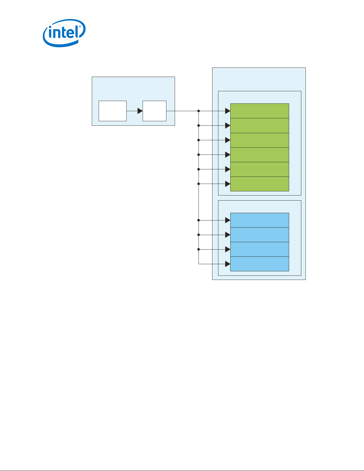
Figure 32. 10X12.5 Gbps xN Bonding
Transceiver PLL
Instance (6.25 GHz)
ATX PLL
Native PHY Instance
(10 Ch Bonded 12.5 Gbps)
TX Channel
TX Channel
TX Channel
TX Channel
TX Channel
TX Channel
TX Channel
Transceiver Bank 2
TX Channel
TX Channel
TX Channel
Master
CGB
xN
Transceiver Bank 1
2. Implementing Protocols in Arria 10 Transceivers
UG-01143 | 2018.06.15
2.5.2.2. TX Multi-Lane Bonding and RX Multi-Lane Deskew Alignment State Machine
Note:
Related Information
• Implementing x6/xN Bonding Mode on page 404
For detailed information on xN bonding limitations
• Using PLLs and Clock Networks on page 398
For more information about implementing PLLs and clocks
The Interlaken configuration sets the enhanced PCS TX and RX FIFOs in Interlaken
elastic buffer mode. In this mode of operation, TX and RX FIFO control and status port
signals are provided to the FPGA fabric. Connect these signals to the MAC layer as
required by the protocol. Based on these FIFO status and control signals, you can
implement the multi-lane deskew alignment state machine in the FPGA fabric to
control the transceiver RX FIFO block.
You must also implement the soft bonding logic to control the transceiver TX FIFO
block.
Intel® Arria® 10 Transceiver PHY User Guide
98
Page 99

2. Implementing Protocols in Arria 10 Transceivers
UG-01143 | 2018.06.15
2.5.2.2.1. TX FIFO Soft Bonding
The MAC layer logic and TX soft bonding logic control the writing of the Interlaken
word to the TX FIFO with tx_enh_data_valid (functions as a TX FIFO write enable)
by monitoring the TX FIFO flags (tx_fifo_full, tx_fifo_pfull,
tx_fifo_empty, tx_fifo_pempty, and so forth). On the TX FIFO read side, a read
enable is controlled by the frame generator. If tx_enh_frame_burst_en is asserted
high, the frame generator reads data from the TX FIFO.
A TX FIFO pre-fill stage must be implemented to perform the TX channel soft bonding.
The following figure shows the state of the pre-fill process.
Intel® Arria® 10 Transceiver PHY User Guide
99
Page 100
Figure 33. TX Soft Bonding Flow
Exit from
tx_digitalreset
Deassert all lanes tx_enh_frame_burst_en
Assert all lanes tx_enh_data_valid
Deassert all lanes
tx_enh_data_valid
All lanes
full?
no
yes
Any lane
send new frame?
tx_enh_frame
asserted?
no
yes
no
yes
All lanes
full?
TX FIFO pre-fill
completed
Wait for extra 16
tx_coreclkin cycles
2. Implementing Protocols in Arria 10 Transceivers
UG-01143 | 2018.06.15
The following figure shows that after deasserting tx_digitalreset, TX soft bonding
logic starts filling the TX FIFO until all lanes are full.
Intel® Arria® 10 Transceiver PHY User Guide
100
 Loading...