

Page 1

AN430TX Motherboard
Technical Product Specification
April, 1997
Order Number 282955-001
The AN430TX motherboard may contain design defects or errors known as errata which may cause the product to deviate from published specifications. Current characterized
errata are documented in the AN430TX Motherboard Specification Update.
Page 2

Revision History
Revision
-001
Revision History Date
First release of the AN430TX Motherboard Technical Product Specification. 4/97
This product specification applies only to standard AN430TX motherboards with BIOS
identifier AN430TX0.86A.
Changes to this specification will be published in the AN430TX Motherboard
Specification Update before being incorporated into a revision of this document.
Information in this document is provided in connection with Intel products. No license, express or implied, by estoppel or
otherwise, to any intellectual property rights is granted by this document. Except as provided in Intel’s Terms and Conditions of
Sale for such products, Intel assumes no liability whatsoever, and Intel disclaims any express or implied warranty, relating to
sale and/or use of Intel products including liability or warranties relating to fitness for a particular purpose, merchantability, or
infringement of any patent, copyright or other intellectual property right. Intel products are not intended for use in medical, life
saving, or life sustaining applications.
Intel retains the right to make changes to specifications and product descriptions at any time, without notice.
The AN430TX may contain design defects or errors known as errata which may cause the product to deviate from published
specifications. Current characterized errata are available on request.
Contact your local Intel sales office or your distributor to obtain the latest specifications before placing your product order.
†
Third-party brands and names are the property of their respective owners.
Copies of documents which have an ordering number and are referenced in this document, or other Intel literature, may be
obtained from:
Intel Corporation
P.O. Box 7641
Mt. Prospect, IL 60056-7641
or call in North America 1-800-879-4683, Europe 44-0-1793-431-155, France 44-0-1793-421-777,
Germany 44-0-1793-421-333, other Countries 708-296-9333.
Copyright 1997, Intel Corporation. All rights reserved.
Page 3

Contents
1 Motherboard Description
1.1 Overview...................................................................................................................... 7
1.2 Motherboard Manufacturing Options............................................................................9
1.3 Form Factor ...............................................................................................................10
1.4 I/O Shield...................................................................................................................11
1.5 Microprocessor...........................................................................................................12
1.5.1 Microprocessor Upgrade..............................................................................12
1.6 Memory......................................................................................................................13
1.6.1 Main Memory...............................................................................................13
1.6.2 Second Level Cache ...................................................................................14
1.7 Chipset.......................................................................................................................14
1.7.1 82439TX System Controller (MTXC) ...........................................................14
1.7.2 82371AB PCI ISA IDE Xcelerator (PIIX4) ....................................................15
1.7.3 Universal Serial Bus (USB) Support ............................................................16
1.7.4 IDE Support.................................................................................................16
1.8 Super I/O Controller ...................................................................................................17
1.8.1 Serial Ports..................................................................................................17
1.8.2 Parallel Port.................................................................................................18
1.8.3 Floppy Controller .........................................................................................18
1.8.4 Keyboard and Mouse Interface....................................................................18
1.8.5 Infrared Support...........................................................................................19
1.9 Graphics Subsystem..................................................................................................19
1.9.1 Graphics Controller......................................................................................19
1.9.2 VESA/ATI Multimedia Channel Connector ..................................................20
1.9.3 Brooktree Video Capture Processor ............................................................20
1.9.4 ImpacTV NTSC/PAL Encoder......................................................................21
1.10 Audio Subsystem.......................................................................................................22
1.10.1 Yamaha OPL4-ML.......................................................................................23
1.10.2 Audio Drivers and Utilities............................................................................23
1.10.3 Audio Connectors ........................................................................................23
1.10.4 CD-ROM audio connector............................................................................23
1.11 Motherboard Connectors ...........................................................................................24
1.11.1 Power Supply Connector .............................................................................29
1.11.2 Front panel Connectors ...............................................................................30
1.11.3 Back Panel Connectors ...............................................................................33
1.11.4 Optional TV/Video Riser Card Connectors ..................................................36
1.12 Add-in Board Expansion Connectors .........................................................................38
1.13 Jumper Settings.........................................................................................................41
1.13.1 Processor Configuration (J9C1-C, D) ..........................................................42
1.13.2 Password Clear (J9C1-A) ............................................................................43
1.13.3 Clear CMOS (J9C1-A).................................................................................43
1.13.4 BIOS Setup Access (J9C1-B)......................................................................43
1.13.5 BIOS Recovery (J8A1) ................................................................................43
1.13.6 Processor Voltage (J6M1) ...........................................................................43
iii
Page 4

AN430TX Motherboard Technical Product Specification
1.14 Reliability....................................................................................................................43
1.15 Environmental............................................................................................................44
1.16 Power Consumption...................................................................................................44
1.16.1 Power Supply Considerations......................................................................45
1.17 Regulatory Compliance..............................................................................................45
1.17.1 Safety ..........................................................................................................45
1.17.2 EMI..............................................................................................................46
1.17.3 Product Certification Markings.....................................................................46
2 Motherboard Resources
2.1 Memory Map..............................................................................................................47
2.2 DMA Channels...........................................................................................................47
2.3 I/O Map......................................................................................................................48
2.4 PCI Configuration Space Map....................................................................................50
2.5 Interrupts....................................................................................................................50
2.6 PCI Interrupt Routing Map .........................................................................................51
3 BIOS and Setup Program
3.1 Introduction................................................................................................................53
3.1.1 BIOS Flash Memory Organization ...............................................................53
3.1.2 BIOS Upgrades ...........................................................................................54
3.1.3 Plug and Play: PCI Auto-configuration ........................................................54
3.1.4 PCI IDE Support ..........................................................................................54
3.1.5 ISA Plug and Play........................................................................................55
3.1.6 ISA Legacy Devices.....................................................................................55
3.1.7 Desktop Management Interface...................................................................55
3.1.8 Advanced Power Management....................................................................56
3.1.9 Language Support .......................................................................................56
3.1.10 Boot Options................................................................................................57
3.1.11 OEM Logo or Scan Area..............................................................................57
3.1.12 USB Support................................................................................................57
3.1.13 BIOS Setup Access Jumper ........................................................................57
3.1.14 Recovering BIOS Data ................................................................................58
3.2 BIOS Setup Program .................................................................................................58
3.2.1 Overview of the Setup Menu Screens .........................................................58
3.2.2 Main Menu...................................................................................................59
3.2.3 Primary/Secondary IDE Master/Slave Configuration Submenus .................61
3.2.4 Advanced Menu...........................................................................................63
3.2.5 Security Menu..............................................................................................67
3.2.6 Power Menu ................................................................................................68
3.2.7 Boot Menu ...................................................................................................68
3.2.8 Exit Menu.....................................................................................................70
4 Error Messages
4.1 BIOS Error Messages ................................................................................................71
4.2 Port 80h POST Codes ...............................................................................................72
iv
Page 5

5 Specifications and Online Support
5.1 Specifications.............................................................................................................79
5.2 Online Support...........................................................................................................80
Figures
1. Motherboard Components ...........................................................................................8
2. Motherboard Dimensions...........................................................................................10
3. Back Panel I/O Shield Dimensions ............................................................................11
4. Motherboard Connectors ...........................................................................................24
5. Front Panel I/O Connectors .......................................................................................30
6. Back Panel I/O Connectors........................................................................................33
7. TV/Video Riser Card Connectors...............................................................................36
8. Jumper Locations.......................................................................................................41
Tables
1. ATI-264GT Rage II+ Maximum Refresh Rates at Different Resolutions ....................20
2. Standard CD-ROM Audio Connector (J2G2) .............................................................25
3. Optional ATAPI Audio Connector (J2G1)...................................................................25
4. Line-In Audio Input Connector (J2H3)........................................................................25
5. Telephony Connector (J2H4).....................................................................................25
6. Serial Port 2 Header (J2J1)........................................................................................25
7. CPU Fan Connector (J6M2).......................................................................................26
8. Floppy Drive Connector (J7L2) ..................................................................................26
9. Optional Video Capture Input Connector (J7B1) ........................................................26
10. GPIO Header (J9A1)..................................................................................................27
11. PCI IDE Connectors (J9H1, J10H1)...........................................................................27
12. System Fan Connector (J10A1).................................................................................27
13. Optional VESA/ATI Multimedia Channel Connector (J5F1) .......................................28
14. Optional Video Riser Header (J3F1) ..........................................................................28
15. Power Supply Connector (J7L1) ................................................................................29
16. Front Panel I/O Connectors .......................................................................................31
17. PS/2 Keyboard and Mouse Connectors .....................................................................34
18. USB Connectors ........................................................................................................34
19. Parallel Port Connector..............................................................................................34
20. Serial Port Connector.................................................................................................34
21. Optional VGA Video Monitor Connector ....................................................................35
22. MIDI / Game Port Connector......................................................................................35
23. S-Video Out Connector..............................................................................................36
24. RCA Composite Video Out Connector .......................................................................36
25. S-Video In and I2C Connector...................................................................................37
26. RCA Composite Video In Connector..........................................................................37
27. PCI Bus Connectors ..................................................................................................38
28. ISA Bus Connectors...................................................................................................39
29. Jumper Settings.........................................................................................................42
30. Jumper Settings for Processor and Bus Frequencies ................................................42
31. Motherboard Environmental Specifications ................................................................44
32. DC Voltage.................................................................................................................44
33. Power Usage for a static Windows 95 Desktop .........................................................44
34. Memory Map..............................................................................................................47
Contents
v
Page 6

AN430TX Motherboard Technical Product Specification
35. DMA Channels...........................................................................................................47
36. I/O Map......................................................................................................................48
37. PCI Configuration Space Map....................................................................................50
38. Interrupts....................................................................................................................50
39. PCI Interrupt Routing Map .........................................................................................51
40. Flash Memory Organization .......................................................................................53
41. Recommendations for Configuring an ATAPI Device.................................................55
42. Overview of the Setup Menu Screens........................................................................59
43. BIOS Error Messages ................................................................................................71
44. Port 80h Codes..........................................................................................................73
45. Compliance with Specifications..................................................................................79
vi
Page 7

1 Motherboard Description
1.1 Overview
The AN430TX motherboard supports Pentium processors and Pentium processors with MMX
technology. The motherboard features:
• ATX form factor
• Socket 7 Pentium OverDrive
Main Memory
• Two 168-pin DIMM sockets
• Support for up to 256 MB of:
extended data out (EDO) memory
unbuffered 4-clock synchronous DRAM (SDRAM) memory
• Up to 64 MB of main memory cacheable
Second Level Cache Memory
• 512 KB pipeline burst static RAM (PBSRAM) soldered to the motherboard
Chipset and PCI/IDE Interface
• Intel 82430TX PCIset
• Integrated PCI bus mastering controller
• Two fast IDE interfaces
• Support for up to four IDE drives or devices
• Support for Ultra DMA/33 drives
• Support for LS-120 removable media IDE drives
processor socket
I/O Features
• PC87307VUL I/O controller
• Integrates standard I/O functions: floppy drive interface, one multimode parallel port, two
FIFO serial ports, keyboard and mouse controller, IrDA
• Support for two Universal Serial Bus (USB) interfaces
Expansion Slots
• Standard version (without video option):
Three PCI
Two ISA
One shared PCI/ISA
• With optional video subsystem:
Three PCI
Three ISA
Video riser (required for TV-out and/or video capture)
†
-compatible interface
7
Page 8
AN430TX Motherboard Technical Product Specification
Audio Subsystem
• Yamaha OPL3-SA3 3-D audio codec soldered to the motherboard
• Yamaha OPL4-ML wavetable synthesizer soldered to the motherboard
Video Subsystem
• Optional ATI
†
-264GT Rage II+ 3-D graphics controller
• Optional Brooktree Bt829A video capture processor
• Optional ATI-ImpacTV
• Optional VESA
†
/ATI Multimedia Channel connector
†
NTSC/PAL TV-out encoder
Other features
• Plug and Play compatible
• Support for Advanced Power Management
Software drivers and utilities are available from Intel.
C FE
DBA
JJ
HH
GG
FF
EE
DD
CC
BB
AA
G
II
Z
Y
W T
X
U R
V
Sec.
Pri.
S
Q
H
I
J
K
L
M
N
O
P
OM06169
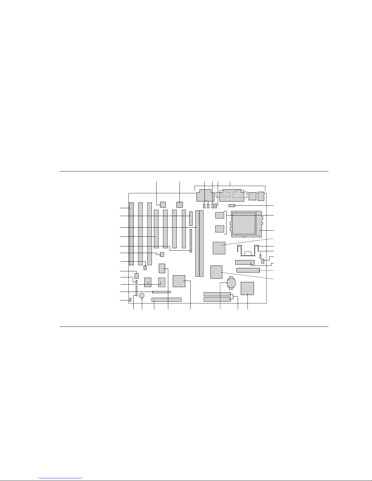
Figure 1. Motherboard Components
8
Page 9

Motherboard Description
A. Yamaha OPL3-SA3 audio codec S. Battery
B. Yamaha OPL4-ML component T. Optional ATI-264GT Rage II+ graphics controller
C. CD-ROM audio connector U. Optional Brooktree Bt829A video capture processor
D. Line-in audio input connector V. Front panel header
E. Telephony connector W. Onboard speaker
F. Back panel I/O connectors X. GPIO header
G. Serial port 2 header Y. System fan connector
H. 512 KB PBSRAM cache Z. Configuration jumper block
I. Socket 7 Pentium processor socket AA. Optional 2 MB of SGRAM video memory
J. 82430TX MTXC system controller BB. BIOS recovery jumper
K. Linear voltage regulator CC. 2 Mbit TSOP Flash memory device
L. Processor voltage jumper DD. Optional Video capture input connector
M. Fan connector EE. Optional ATI-ImpacTV NTSC/PAL TV-out device
N. Power connector FF. Optional VESA/ATI Multimedia Channel connector
O. Floppy drive connector GG. PCI connectors
P. 82430TX PIIX4 PCI ISA IDE Xcelerator HH. DIMM sockets
Q. PC87307VUL I/O controller II. Optional video riser card header
R. IDE connectors JJ. ISA connectors
1.2 Motherboard Manufacturing Options
• ATI-264GT Rage II+ 3-D graphics controller with 2 MB of SGRAM
• Brooktree Bt829A video capture processor
• ATI-ImpacTV NTSC/PAL TV-out encoder
• VESA/ATI Multimedia Channel connector
• Unshrouded floppy disk and IDE controller connectors
9
Page 10
AN430TX Motherboard Technical Product Specification
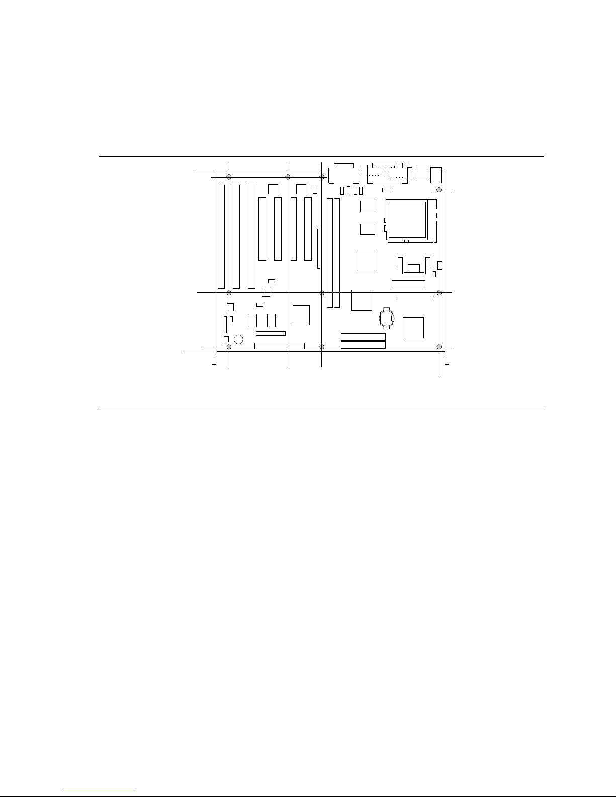
1.3 Form Factor
The motherboard is designed to fit into a standard ATX form factor chassis. Figure 2 illustrates the
form factor for the motherboard. The location of the I/O connectors and mounting holes are in
strict compliance with the ATX specification (see Section 5.1).
9.04
8.95
8.05
2.85
0.25
0.0
0.65
0.0
3.10
4.90
Figure 2. Motherboard Dimensions
11.35
11.10
OM06161
10
Page 11
Motherboard Description
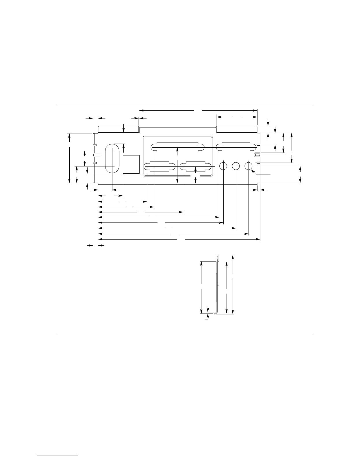
1.4 I/O Shield
The back panel I/O shield for the AN430TX motherboard must meet specific dimensional and
material requirements. Computers based on this motherboard need the back panel I/O shield in
order to pass certification testing. Figure 3 shows the critical dimensions for the I/O shield and
indicates the position of each cutout. The example shown is chassis-specific and will not
necessarily work with other chassis types.
4.610
1.590
0.295
1.955
0.133
0.597
0.200
0.478
1.407
0.458
0.768
1.158
0.671
0.395
0.553
0.990
1.911
2.184
3.327
4.735
4.899
0.193
Note: Material = 0.010 ±.0.001 Thick Stainless Steel, Half Hard
5.391
5.883
6.533
0.652
2.055
0.050
2.326
2.023
0.120
Left-end View
0.306 Dia (3)
0.666
OM05669
Figure 3. Back Panel I/O Shield Dimensions
11
Page 12
AN430TX Motherboard Technical Product Specification
OM05908
1.5 Microprocessor
The motherboard supports:
• Pentium processors operating at 90, 100, 120, 133, 150, 166, and 200 MHz
• Pentium processors with MMX technology operating at 166, and 200 MHz
An onboard voltage regulator derives the necessary voltage from the computer’s power supply and
enables use of standard or VRE-specified processors. The motherboard automatically detects the
type of processor (Pentium processor or Pentium processor with MMX technology).
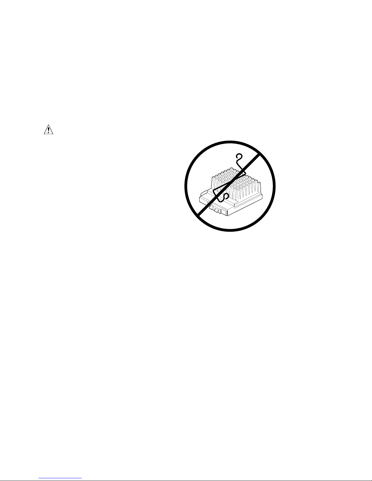
CAUTION
If you use clips to secure a heat sink
to the processor, do not use bail-wire
style heat sink clips, such as the type
shown in the figure to the right.
These clips have been known to
damage the motherboard when
installed or removed incorrectly.
1.5.1 Microprocessor Upgrade
The motherboard has a 321-pin Socket 7 zero insertion force (ZIF) microprocessor socket.
Socket 7 supports upgrades to higher performance Pentium OverDrive processors not supported by
Socket 5.
12
Page 13

Motherboard Description
1.6 Memory
1.6.1 Main Memory
The motherboard has two 168-pin DIMM sockets. Memory can be installed in one or two sockets.
Minimum memory size is 8 MB. Maximum memory size is 256 MB. The BIOS automatically
detects memory type, size, and speed so no jumper settings are required.
The motherboard supports the following:
• 168-pin 3.3 V DIMMs with tin-plated contacts
• 60 and 66 MHz bus speeds
• 60 ns 3.3V EDO DRAM
• 60 ns unrestricted CAS Latency 2 unbuffered 4-clock 3.3V SDRAM
• Caching for the first 64 MB of main memory
• 64-bit data path
• Single- or double-sided DIMMs in the following sizes:
DIMM Size Type Configuration Technology
8 MB 60 ns EDO 1M x 64 16 Mbit
16 MB 60 ns EDO 2M x 64 16 Mbit
32 MB 60 ns EDO 4M x 64 16 Mbit
64 MB 60 ns EDO 8M x 64 16 Mbit
8 MB CAS Latency 2 SDRAM 1M x 64 16 Mbit
16 MB CAS Latency 2 SDRAM 2M x 64 16 Mbit
32 MB CAS Latency 2 SDRAM 4M x 64 16 Mbit
64 MB CAS Latency 2 SDRAM 8M x 64 64 Mbit
128 MB CAS Latency 2 SDRAM 16M x 64 64 Mbit
Memory type, size, and speed can vary between sockets, so EDO and SDRAM can be installed on
the same motherboard. Parity (x 72) DIMMs can be installed but are not recommended for the
following reasons:
• The motherboard does not provide parity checking or ECC
• Parity DIMMs cause excessive capacitive loading on memory data and address lines
1.6.1.1 EDO DRAM
EDO DRAM improves memory read performance by holding the memory data valid until the next
CAS# falling edge, unlike fast page mode DRAM, which tri-states the memory data when CAS#
negates to precharge for the next memory cycle. With EDO DRAM, the CAS# precharge overlaps
the data-valid time, which allows CAS# to negate earlier while still satisfying the memory datavalid window.
13
Page 14

AN430TX Motherboard Technical Product Specification
1.6.1.2 SDRAM
Synchronous DRAM (SDRAM) is designed to improve main memory performance. Unlike fast
page or EDO DRAM, SDRAM is synchronous with the memory clock. This simplifies the timing
design and increases memory speed because all timing is dependent on the number of memory
clock cycles. SDRAM DIMM should meet the Intel 4-clock 66 MHz 64-bit unbuffered SDRAM
DIMM v1.0 specification.
CAUTION
The board does not support SDRAM DIMMs with an n x 4 DRAM base due to loading anomalies.
For example, a DIMM that uses sixteen 16 Mbit x 4 devices should not be used.
NOTE
✏
The AN430TX supports unbuffered, 4-clock 3.3V SDRAM DIMMs only. Buffered, 5V, or 2-clock
SDRAM DIMMs cannot be used.
1.6.2 Second Level Cache
The 512 KB direct-mapped write-back L2 cache consists of two 64K x 32 global write enable
(GWE) pipeline burst asynchronous RAMs (PBSRAMs) and a 32K x 8 external tag SRAM. These
devices are soldered to the motherboard.
1.7 Chipset
The Intel 82430TX PCIset consists of the 82439TX System Controller (MTXC) device and the
82371AB PCI ISA IDE Xcelerator (PIIX4) device.
1.7.1 82439TX System Controller (MTXC)
The MTXC integrates the cache and main memory DRAM control functions and provides bus
control to handle transfers between the processor, cache, main memory, and the PCI bus. The
MTXC allows PCI masters to achieve full PCI bandwidth by using the snoop ahead feature. For
increased system performance the MTXC integrates posted write and read prefetch buffers. The
MTXC comes in a 324-pin MBGA package that features:
• Microprocessor interface control
• Integrated L2 write-back cache controller
Supports pipeline burst SRAM
64 MB maximum DRAM cacheability
Direct mapped organization—write back only
Cache hit read/write cycle timings at 3-1-1-1
Back to back read/write cycles at 3-1-1-1-1-1-1-1
14
Page 15

Motherboard Description
• Integrated DRAM controller
8 MB to 256 MB main memory
64-Mbit DRAM/SDRAM technology support
3.3V EDO and unbuffered synchronous DRAM support
Non-parity (x64) support only
• Fully synchronous minimum latency PCI bus interface
PCI compliance (see Section 5.1 for compliance level)
30 and 33 MHz bus speeds
PCI to DRAM data throughput at greater than 100 MB/sec
Up to four PCI masters in addition to the PIIX4
• Power management control
Provides PCI CLKRUN# signal to control memory clock on the PCI bus (on/off)
Internal clock control (gated off if no host or PCI bus activity)
1.7.2 82371AB PCI ISA IDE Xcelerator (PIIX4)
The Intel 82371AB PCI ISA IDE Xcelerator (PIIX4) is a multifunction PCI device implementing a
PCI to ISA bridge, PCI IDE functionality, a Universal Serial Bus (USB) host/hub function, and
Enhanced Power Management. The PIIX4 comes in a 324-pin MBGA package that features:
• Multifunction PCI to ISA bridge
Supports the PCI bus at 30 and 33 MHz
PCI compliant (see section 5.1 for compliance level)
Full ISA or extended I/O (EIO) bus support
• USB controller
Two USB ports (see section 5.1 for compliance level)
Supports legacy keyboard and mouse
Supports UHCI design guide revision 1.1 interface
• Integrated dual-channel enhanced IDE interface
Support for up to four IDE devices
PIO Mode 4 transfers at up to 14 MB/sec
Supports “Ultra DMA/33” synchronous DMA mode transfers up to 33 MB/sec
Integrated 8 x 32-bit buffer for bus master PCI IDE burst transfers
Bus master mode
• Enhanced DMA controller
Two 8237-based DMA controllers
Supports PCI DMA with three PC/PCI channels and distributed DMA protocols
Fast type-F DMA for reduced PCI bus usage
• Interrupt controller based on 82C59
Support for 15 interrupts
Programmable for edge/level sensitivity
• Power management logic
Sleep/resume logic
Supports thermal alarm
Support for wake on modem through Ring Indicate input
15
Page 16

AN430TX Motherboard Technical Product Specification
• Real-Time Clock
256 byte battery-backed CMOS SRAM
Includes date alarm
• 16-bit counters/timers based on 82C54
1.7.3 Universal Serial Bus (USB) Support
The motherboard features two USB ports. The ports permit the direct connection of two USB
peripherals without an external hub. If more devices are required, an external hub can be
connected to either of the built-in ports. The motherboard fully supports the standard universal
host controller interface (UHCI) and uses standard software drivers that are UHCI-compatible.
Features of the USB include:
• Self-identifying, hot pluggable peripherals
• Automatic mapping of function to driver and configuration
• Support for isochronous and asynchronous transfer types over the same set of wires
• Support for up to 127 physical devices
• Guaranteed bandwidth and low latencies appropriate for telephony, audio, and other
applications
• Error handling and fault recovery mechanisms built into protocol
NOTE
✏
Computers that have an unshielded cable attached to the USB port might not meet FCC Class B
requirements, even if no device or a low speed (sub-channel) USB device is attached to the cable.
Use shielded cable that meets the requirements for high speed (fully rated) devices.
1.7.4 IDE Support
The motherboard has two independent bus mastering PCI IDE interfaces that support PIO Mode 3,
PIO Mode 4, ATA-33 (Ultra DMA/33), and ATAPI (e.g., CD-ROM) devices. The BIOS supports
Logical Block Addressing (LBA) and Extended Cylinder Head Sector (ECHS) translation modes.
IDE device transfer rate and translation mode are automatically detected by the BIOS.
Normally, programmed I/O operations require a substantial amount of processor bandwidth;
however, in true multi-tasking operating systems like Windows
mastering IDE can be devoted to other tasks while disk transfers are occurring.
1.7.4.1 LS-120 Support
LS-120 MB Diskette technology enables users to store 120 MB of data on a single, 3.5-inch
removable diskette. LS-120 technology is backward (both read and write) compatible with
1.44 MB and 720 KB DOS-formatted diskettes and is supported by Windows 95 and Windows
†
operating systems.
NT
The AN430TX motherboard allows connection of an LS-120 compatible drive and a standard
3.5-inch diskette drive. The LS-120 drive can be configured as a boot device, if selected in the
BIOS setup utility.
†
95, the bandwidth freed by bus
16
Page 17

Motherboard Description
NOTE
✏
If you connect an LS-120 drive to an IDE connector and configure it as the “A” drive and
configure a standard 3.5-inch floppy as a “B” drive, the standard floppy must be connected to the
floppy drive cable’s “A” connector (the connector at the end of the cable).
1.8 Super I/O Controller
The PC87307VUL Super I/O Controller from National Semiconductor is an ISA Plug and Play
compatible (see section 5.1 for compliance level), multifunction I/O device that provides the
following features:
• Serial ports:
Two 16450/16550A-software compatible UARTs
Send/receive 16-byte FIFO
Four 8-bit DMA options for the UART with Slow Infrared Support (USI)
Ring indicator support for both serial ports
• Multimode bidirectional parallel port
Standard mode, IBM
Enhanced Parallel Port (EPP) mode with BIOS and driver support
High-speed Extended Capabilities Port (ECP) mode
• Floppy disk controller
DP8473 and N82077 compatible
16 byte FIFO
PS/2
CMOS disk input and output logic
High performance digital data separator (DDS)
PC-AT
• Keyboard and mouse controller
Industry standard 8042A compatible
General purpose microcontroller
8 bit internal data bus
• Support for an IrDA and Consumer IR-compliant infrared interface
†
diagnostic register support
†
and PS/2 drive mode support
†
and Centronics† compatible
By default, the I/O controller interfaces are automatically configured during boot up. The I/O
controller can also be manually configured in the Setup program.
1.8.1 Serial Ports
The motherboard has one 9-pin D-Sub serial port connector located on the back panel, and one
keyed 10-pin header located on the motherboard for cabling to the back panel. The 16540 and
16550A compatible UARTs support data transfers at speeds up to 921.6 Kbits/sec, while the
extended UART mode supports data rates up to 1.5 Mbits/sec.
17
Page 18

AN430TX Motherboard Technical Product Specification
1.8.2 Parallel Port
The connector for the multimode bidirectional parallel port is a 25-pin D-Sub connector located on
the back panel of the motherboard. In the Setup program, there are four options for parallel port
operation:
• Compatible (standard mode)
• Bidirectional (PS/2-compatible)
• Bidirectional Enhanced Parallel Port (EPP) (see Section 5.1 for EPP specification compliance
level)
• Bidirectional Extended Capabilities Port (ECP)
1.8.3 Floppy Controller
The I/O controller is software compatible with the DP8473 and N82077 floppy drive controllers
and supports both PC-AT and PS/2 modes. In the Setup program, the floppy interface can be
configured for the following floppy drive capacities and sizes:
• 360 KB, 5.25-inch
• 1.2 MB, 5.25-inch
• 720 KB, 3.5-inch
• 1.2 MB, 3.5-inch (driver required)
• 1.25/1.44 MB, 3.5-inch
• 2.88 MB, 3.5-inch
1.8.4 Keyboard and Mouse Interface
PS/2 keyboard and mouse connectors are located on the back panel of the motherboard.
The 5 V lines to these connectors are protected with a PolySwitch
fuse, reestablishes the connection after an over-current condition is removed. While this device
eliminates the possibility of having to replace a fuse, power to the computer should be turned off
before connecting or disconnecting a keyboard or mouse.
NOTE
✏
You can plug the mouse and keyboard into either connector.
The keyboard controller contains the Phoenix keyboard and mouse controller code, which provides
the traditional keyboard and mouse control functions, and also supports Power On/Reset password
protection. A Power On/Reset password can be specified in the Setup program.
The keyboard controller also supports the following hot-key sequences:
• <Ctrl><Alt><Del> Software reset. This key sequence resets the computer’s software by
jumping to the beginning of the BIOS code and running the Power On Self Test (POST).
†
circuit that, like a self-healing
18
Page 19

Motherboard Description
1.8.5 Infrared Support
The motherboard has a 6-pin header that supports Hewlett Packard† HSDL-1000 compatible
infrared (IR) transmitters/receivers. In the Setup program, Serial Port 2 can be directed to a
connected IR device. The connection can be used to transfer files to or from portable devices like
laptops, PDAs and printers. The Infrared Data Association (IrDA) specification supports data
transfers of 115 Kbits/sec at a distance of 1 meter. See section 5.1 for IrDA specification
compliance level.
1.8.5.1 Consumer Infrared Support
The motherboard has a dedicated signal pin that supports Consumer Infrared (IR) devices (remote
controls). The signal pin supports receive only. Consumer IR devices can be used to control
telephony functions and multimedia operations like volume and CD track changes. In this mode,
data rates of up to 685.57 Kbits/sec are supported. A software and hardware interface is needed to
use this feature.
1.9 Graphics Subsystem
The optional onboard graphics subsystem features the ATI-264GT Rage II+ graphics controller.
1.9.1 Graphics Controller
The ATI-264GT Rage II+ provides the following features:
• Drawing coprocessor that operates concurrently with the host processor
• Optional video coprocessor that enables simultaneous display of 24 bits per pixel (bpp) video
and 8 bpp graphics
• VGA
• PCI compliant
• Support for power management
• Support for VESA Display Data Channel (DDC2B)
• Video scaler, color space converter, true color palette
• Triple-clock synthesizer
• Support for ATI multimedia feature connector
• 3-D graphics capability
• PCI bus master
1.9.1.1 Video Memory
The motherboard supports 2 MB of 66MHz (15 ns burst mode cycle time) SGRAM for video
memory, soldered to the board. There are no upgrade options for video memory.
†
and VESA compatibility
19
Page 20

AN430TX Motherboard Technical Product Specification
1.9.1.2 Resolutions and Refresh Rates
Table 1. ATI-264GT Rage II+ Maximum Refresh Rates at Different Resolutions
2 MB Memory Maximum Refresh Rate (Hz) At:
4-bit Color
Resolution
640 x 480 160 160 160 160
800 x 600 160 160 160 160
1024 x 768 160 160 160 not supported
1152 x 864 160 160 160 not supported
1280 x 1024 160 160 160 not supported
(16 Colors)
8-bit Color
(256 Colors)
16-bit Color
(64K Colors)
24-bit Color
(16M Colors)
1.9.1.3 Graphics Drivers and Utilities
Graphics drivers and common graphics utilities are available for Windows 3.x, Windows 95, and
Windows NT. Drivers and utilities are available from Intel’s World Wide Web site (see
Section 5.2).
1.9.2 VESA/ATI Multimedia Channel Connector
The motherboard has an optional 40-pin VESA/ATI Multimedia Channel connector that uses
26 pins for the VESA standard bus and 12 pins for the ATI Enhanced Visual Architecture bus. The
connector features a shared frame buffer interface and a Local Peripheral Bus (LPB) with a
bidirectional interface that supports video companion devices like MPEG/live video decoders.
1.9.3 Brooktree Video Capture Processor
The motherboard features an optional Brooktree Bt829A Video Capture Processor for digitizing
analog NTSC/PAL/SECAM input signals from TV tuners, VCRs, cameras, and other sources of
composite or Y/C video. The Bt829A has the mixed signal circuitry required to convert an analog
composite signal into a scaled digital video stream supporting several video formats, resolutions
and frame rates. The Bt829A features include:
• Single-chip composite/S-Video NTSC/PAL/SECAM to YCrCb digitizer
• Square pixel and CCIR601 resolution for NTSC, PAL, and SECAM
• Chroma comb filtering
• Horizontal and vertical filtered scaling
• Programmable hue, brightness, saturation, and contrast
• User-programmable cropping of the video window
• 2x oversampling
• Two-wire I
• 8- or 16-bit pixel interface
• Automatic NTSC/PAL format detection
• Automatic gain control
2
C bus interface
20
Page 21

Motherboard Description
The motherboard provides two inputs for video on the video riser card I/O panel: an RCA input
connector for composite video signals, and a 7-pin mini-DIN connector for S-Video signals and
2
Inter-Integrated Circuit (I
C) signals.
The Bt829A’s registers are accessed using the I
device. To reprogram the default settings, you must connect an I
2
C/S-Video connector. The I2C serial clock and data lines transfer data from the master device at
I
2
C interface. The Bt829A operates as an I2C slave
2
C master to the 7-pin mini-DIN
a rate of 100 Kbits/sec.
1.9.3.1 Video Capture Input Connector
A 1x4 pin connector is available on the motherboard for applying a composite video signal (from a
TV Tuner add-in card, for example) to the input of the Brooktree Bt829A Video Capture device.
2
Two pins are dedicated to external control capability via the I
C protocol using serial clock (SCL)
and serial data (SDA) pins.
1.9.3.2 Video Capture Drivers and Utilities
Video capture software and utilities are available from Intel’s World Wide Web site (see
Section 5.2).
1.9.4 ImpacTV NTSC/PAL Encoder
The optional ATI-ImpacTV NTSC/PAL Encoder is an ASIC that provides a TV-out interface for
the ATI-264GTB 3D Rage II+ multimedia graphics accelerators. Quality issues such as image
flicker, illegible text and low-definition graphics are controlled through on-chip circuitry for
scaling, flicker removal, and artifact suppression. Features include:
• Circuitry for producing interlaced images with flicker removed
• Circuitry for eliminating dot crawl
• Filters for bringing out detail in fine text while suppressing color artifacts
• Support for both NTSC and PAL formats
• Filters that ensure signal bandwidth does not exceed TV standards
• Fully programmable timing that enables NTSC or PAL signals to be generated from monitor
resolutions that include 320x200, 320x240, 320x350, 320x400, 360x200, 360x240, 360x400,
360x440, 512x384, 640x350, 640x400, 640x480, 720x350, 720x400, 720x480, and 800x600
• Simultaneous display of images on both a TV and a PC monitor
• Independent horizontal positioning of the TV image and the PC monitor image
• Independent vertical positioning of the TV image and the PC monitor image
• Independent horizontal scaling of the TV image and the PC monitor image
• Power management for full VESA DPMS and EPA Energy Star compliance
• Automatic power down of the ASIC at initialization if a TV is not detected
• Support for both composite and S-Video connectors
The motherboard provides two outputs for video on the video riser card I/O panel: an RCA
connector for composite video-out signals and a 4-pin mini-DIN connector for S-Video output
signals.
21
Page 22

AN430TX Motherboard Technical Product Specification
NOTE
✏
A video riser card is required for TV outputs and video capture inputs (shown in Figure 7).
1.10 Audio Subsystem
The onboard audio subsystem features the Yamaha OPL† YMF715, a 100-pin SQFP audio chip. It
integrates a 16-bit audio codec, OPL3 FM synthesis and its DAC, 3-D enhanced stereo controller,
and an interface for MPU-401 and a joystick. The YMF715 provides all the digital audio and
analog mixing functions needed for recording and playing sound on personal computers. It
features the following:
• Integrated 3-D enhanced stereo controller including all required analog components
• Stereo analog-to-digital and digital-to-analog converters
• Analog mixing, anti-aliasing, and reconstruction filters
• Support for 16-bit address decode
• Line, microphone, mono, and modem inputs
• ADPCM, A-law or µlaw digital audio compression/decompression
• Full digital control of all mixer and volume control functions
• Software switching between rear panel Mic In and Line In connectors
• Plug and Play compatibility
• Sound Blaster
• Pin compatible with the Yamaha YMF711
†
and Windows Sound System compatibility
The following table shows the IRQ, DMA channel, and base I/O address options for the audio
subsystem. These options are automatically chosen by the Plug and Play interface, so there are no
default settings.
IRQ
Resource
Sound Blaster
(DMA playback, DMA shared with
Windows Sound System capture)
Windows Sound System
(DMA playback)
MPU-401
(IRQ shared with Sound Blaster)
MIDI / Game Port 201h
†
AdLib
(Options)
5
7
9
10
11
5
7
9
10
11
DMA Channel
(Options)
0
1
3
0
1
3
I/O Address
(Options)
220h
240h
220-280h
530h
E80h
530-F48h
330h
300h
300-334h
201-211h
388h
388-3F8h
22
Page 23

Motherboard Description
1.10.1 Yamaha OPL4-ML
The Yamaha OPL4-ML wavetable is a ROM table containing live instrument sound samples.
Wave synthesis results in richer and more realistic sounds then that of FM synthesis.
1.10.2 Audio Drivers and Utilities
Audio software and utilities are available from Intel’s World Wide Web site (see Section 5.2).
1.10.3 Audio Connectors
The board has these audio connectors:
• Back panel audio jacks (Line In, Line Out, Mic In)
• CD-ROM audio connector (either standard CD or optional ATAPI styles provided)
• Telephony connector (ATAPI style only)
• Line-in audio input connector (ATAPI style only)
1.10.4 CD-ROM audio connector
A 1 x 4-pin connector is available for connecting the audio output of an internal CD-ROM
connector to the audio subsystem’s mixer. The connector is compatible with most cables supplied
with ATAPI CD-ROM headers designed to connect to audio add-in cards.
23
Page 24
AN430TX Motherboard Technical Product Specification
1.11 Motherboard Connectors
Figure 4 shows the connectors on the motherboard.
Video
Riser
(Optional)
VESA/ATI
Multimedia
Channel
(Optional)
2
24
1
25
27
J3F1
J5F1
1
23
2
28
Connectors(4)
J4C1, J4D1
J4E1, J4E2
ISA
Connectors(3)
J4A1, J4B1
J4B2
PCI
J2G2
1
4
CD-ROM
Audio
J2G1
4
1
ATAPI
Audio
(Optional)
Sec.
Pri.
J2H3
4
1
Line-in
Audio
J2H4
4
1
Serial Port 2
9
8
CPU
Fan
3
1
J6M2
1
11
Telephony
1
2
J2J1
J7L1
Power
10
20
39
J10A1
Chassis
1
3
Fan
40
J9A1
1
8
GPIO
J7B1
1
4
Video
Capture
Input
(Optional)
2
1
J9H1
J10H1
20
IDE(2)
Secondary
Primary
40
39
J7L2
234
1335
Floppy Drive
OM06165
Figure 4. Motherboard Connectors
24
Page 25

Table 2. Standard CD-ROM Audio
Connector (J2G2)
Pin Signal Name
1 Ground
2 CD audio left channel
3 Ground
4 CD audio right channel
Table 3. Optional ATAPI Audio Connector
(J2G1)
Pin Signal Name
1 CD audio left channel
2 Ground
3 Ground
4 CD audio right channel
Motherboard Description
Table 4. Line-In Audio Input Connector
(J2H3)
Pin Signal Name
1 Left channel audio in
2 Ground
3 Ground
4 Right channel audio in
Table 5. Telephony Connector (J2H4)
Pin Signal Name
1 Mono output
2 Ground
3 Ground
4 MIC input
Table 6. Serial Port 2 Header (J2J1)
Pin Signal Name Pin Signal Name
1 DCD# 2 DSR#
3 Serial In 4 RTS#
5 Serial Out 6 CTS#
7 DTR# 8 RI#
9 Ground 10 Key
25
Page 26

AN430TX Motherboard Technical Product Specification
Table 7. CPU Fan Connector (J6M2)
Pin Signal Name
1 Ground
2 +12 V
3 No connect
Table 8. Floppy Drive Connector (J7L2)
Pin Signal Name Pin Signal Name
1 Ground 2 DENSEL
3 Ground 4 Reserved
5 Key 6 FDEDIN#
7 Ground 8 FDINDX# (Index)
9 Ground 10 FDM00# (Motor enable A)
11 Ground 12 FDDS1# (Drive select B)
13 Ground 14 FDDS0# (Drive select A)
15 Ground 16 FDM01# (Motor enable B)
17 MSEN1 18 FDDIR#
19 Ground 20 FDSTEP#
21 Ground 22 FDWD# (Write data)
23 Ground 24 FDWE# (Write gate)
25 Ground 26 FDTRK0# (Track 0)
27 MSEN0 28 FDWPD# (Write protect)
29 Ground 30 FDRDATA# (Read data)
31 Ground 32 FDHEAD# (Side 1 select)
33 Ground 34 DSKCHG# (Diskette change)
Table 9. Optional Video Capture Input
Connector (J7B1)
Pin Signal Name
1 Composite Video In
2 Ground
3 SCL
4 SDA
26
Page 27

Motherboard Description
Table 10. GPIO Header (J9A1)
Pin Signal Name
1 No connect
2 Key
3 GPIO1_7
4 Ground
5 GPIO1_2
6 Ground
7 GPIO1_1
8 Ground
Table 11. PCI IDE Connectors (J9H1, J10H1)
Pin Signal Name Pin Signal Name
1 Reset IDE 2 Ground
3 Host data 7 4 Host data 8
5 Host data 6 6 Host data 9
7 Host data 5 8 Host data 10
9 Host data 4 10 Host data 11
11 Host data 3 12 Host data 12
13 Host data 2 14 Host data 13
15 Host data 1 16 Host data 14
17 Host data 0 18 Host data 15
19 Ground 20 Key
21 DDRQ0 [DDRQ1] 22 Ground
23 I/O write# 24 Ground
25 I/O read# 26 Ground
27 IOCHRDY 28 Vcc pull-up
29 DDACK0# [DDACK1#] 30 Ground
31 IRQ 14 [IRQ 15] 32 Reserved
33 Address 1 34 Reserved
35 Address 0 36 Address 2
37 Chip select 1P# [Chip select 1S#] 38 Chip Select 3P# [Chip select 3S#]
39 Activity# 40 Ground
NOTE: Signal names in brackets ([ ]) are for the secondary IDE connector
Table 12. System Fan Connector (J10A1)
Pin Signal Name
1 Ground
2 +12 V
3 Ground
27
Page 28

AN430TX Motherboard Technical Product Specification
Table 13. Optional VESA/ATI Multimedia Channel Connector (J5F1)
Pin Signal Name Pin Signal Name
1 Ground 2 Data 0
3 Ground 4 Data 1
5 Ground 6 Data 2
7 Data enable 8 Data 3
9 Sync enable 10 Data 4
11 PCLK enable 12 Data 5
13 SDA 14 Data 6
15 Ground 16 Data 7
17 Ground 18 DCLK
19 Ground 20 BLANK
21 VFCSNS 22 HSYNC
23 SCL 24 VSYNC
25 Key 26 Ground
27 Key 28 Key
29 VCC 30 SA
31 RST 32 SNRDY
33 SAD 34 VMASK
35 No connect 36 AMCREV
37 Ground 38 +12 V
39 No connect 40 No connect
Table 14. Optional Video Riser Header (J3F1)
Pin Signal Name Pin Signal Name
1NC 2NC
3 Ground 4 Composite in
5 Ground 6 Y in
7 Ground 8 SCL
9 Ground 10 SDA
11 Ground 12 C-In
13 Ground 14 +12 V
15 Ground 16 Composite out
17 Ground 18 Luma out
19 Ground 20 Chroma out
21 Ground 22 +5 V
23 NC 24 NC (Reserved)
28
Page 29

Motherboard Description
1.11.1 Power Supply Connector
When used with a power supply that supports remote power on/off, the motherboard can turn off
the computer’s power through software control. Pin 14 of the power supply connector lets the
motherboard recognize a power supply that supports this “soft-off” feature; the power supply must
tie pin 14 to ground.
When the BIOS receives the correct APM command from the operating system, the BIOS turns off
power to the computer. For example, in the Windows 95 Start menu, the user selects Shutdown to
turn off the power.
If power to the computer is interrupted by a power outage or a disconnected power cord, when
power resumes, the computer remains in the off state until the power on switch is pressed.
Table 15. Power Supply Connector (J7L1)
Pin Signal Name Pin Signal Name
1 +3.3 V 11 +3.3 V
2 +3.3 V 12 -12 V
3 Ground 13 Ground
4 +5 V 14 PS-ON# (Power Supply Remote
On/Off Control)
5 Ground 15 Ground
6 +5 V 16 Ground
7 Ground 17 Ground
8 PWRGD (Power Good) 18 -5 V
9 +5 VSB (Standby for real-time clock) 19 +5 V
10 +12 V 20 +5 V
29
Page 30

AN430TX Motherboard Technical Product Specification
1.11.2 Front panel Connectors
The front panel connector includes headers for these I/O connections:
• Speaker
• Reset switch
• Power LED
• Hard drive activity LED
• Infrared (IrDA) port
• Sleep switch
• Power switch
Speaker Reset Pwr LED HD LED Infrared Sleep Pwr On
27 1
OM06166
Figure 5. Front Panel I/O Connectors
30
Page 31

Table 16. Front Panel I/O Connectors
Pin Signal Name Connector
1 SW_ON# Power On
2 Ground
3 SLEEP Sleep/Resume
4 SLEEP_PU (pullup)
5 No connect none
6 +5 V IrDA
7 Key
8 IrRX
9 Ground
10 IrTX
11 CONIR (Consumer IR)
12 No connect none
13 HD_PWR +5 V HD LED
14 Key
15 HD Active#
16 HD_PWR
17 No connect/Key none
18 Ground Sleep/Power LED
19 Key
20 PWR_LED
21 No connect/Key none
22 Ground Reset
23 SW_RST
24 Ground Speaker
25 Key
26 PIEZO_IN
27 SPKR_HDR
Motherboard Description
1.11.2.1 Sleep/Resume
When advanced power management (APM) is enabled in the BIOS and the operating system’s
APM driver is loaded, the computer can enter Sleep (Standby) mode in one of two ways:
• Pressing the optional front panel Sleep/Resume button
• Prolonged inactivity; the timeout period is adjustable in the Setup program
A sleep/resume button is supported by the 2-pin header located on the front panel I/O connector.
The front panel sleep/resume switch must be a momentary SPST type that is normally open.
31
Page 32

AN430TX Motherboard Technical Product Specification
Closing the sleep/resume switch generates a system management interrupt (SMI) to the processor,
which immediately goes into system management mode (SMM). While the computer is in sleep
mode it is fully capable of responding to and servicing external interrupts (such as an incoming
fax) even though the monitor turns on only if a keyboard or mouse interrupt occurs. To reactivate
the computer, or resume, you must press the sleep/resume button again, or use the keyboard or
mouse.
1.11.2.2 Infrared connector
Serial Port 2 can be configured to support an IrDA module connected to this 6-pin header. After
configuring the IrDA interface, you can transfer files to or from portable devices such as laptops,
PDAs, and printers using application software.
1.11.2.3 Hard Drive (HD) LED
You can connect this header to an LED to provide a visual indicator that data is being read from or
written to an IDE hard drive. For the LED to function properly, the IDE drive must be connected
to the onboard IDE controller on the motherboard.
1.11.2.4 Sleep/Power LED
You can connect this header to an LED that will light when the computer is powered on. This
LED will also blink when the computer is in a power-managed state.
1.11.2.5 Reset
You can connect this header to a momentary SPST type switch that is normally open. When the
switch is closed, the board resets and runs the POST.
1.11.2.6 Speaker
A speaker may be installed on the motherboard as a manufacturing option. The speaker option
includes a jumper on pins 26-27 of the front panel connector. You can disable the onboard speaker
by removing the jumper, and you can connect an offboard speaker in its place. The speaker
(onboard or offboard) provides error beep code information during the Power-On Self Test (POST)
in the event that the computer cannot use the video interface. The speaker is not connected to the
audio subsystem, and does not receive output from the audio subsystem.
32
Page 33

1.11.3 Back Panel Connectors
Figure 6 shows the location of the back panel I/O connectors, which include:
• PS/2-style keyboard and mouse connectors
• Two USB connectors
• One parallel port
• One serial port
• Optional video monitor connector
• MIDI/game port
• External audio jacks: Line Out, Line In and Mic In
Motherboard Description
Keyboard
USB 1
Mouse Serial Port 1
USB 0
Figure 6. Back Panel I/O Connectors
Parallel Port
Video
(Optional)
MIDI/Game Port
Line Out Mic In
Line In
OM06167
33
Page 34

AN430TX Motherboard Technical Product Specification
Table 17. PS/2 Keyboard and Mouse
Connectors
Pin Signal Name
1 Data
2 No connect
3 Ground
4 +5 V (fused)
5 Clock
6 No connect
Table 18. USB Connectors
Pin Signal Name
1 Power
2 USBP0# [USBP1#]
3 USBP0 [USBP1]
4 Ground
Table 19. Parallel Port Connector
Pin Signal Name Pin Signal Name
1 Strobe# 14 Auto Feed#
2 Data bit 0 15 Fault#
3 Data bit 1 16 INIT#
4 Data bit 2 17 SLCT IN#
5 Data bit 3 18 Ground
6 Data bit 4 19 Ground
7 Data bit 5 20 Ground
8 Data bit 6 21 Ground
9 Data bit 7 22 Ground
10 ACK# 23 Ground
11 Busy 24 Ground
12 Error 25 Ground
13 Select
Table 20. Serial Port Connector
Pin Signal Name Pin Signal Name
1 DCD# 6 DSR#
2 Serial In 7 RTS#
3 Serial Out 8 CTS#
4 DTR# 9 RI#
5 Ground
34
Page 35

Table 21. Optional VGA Video Monitor Connector
Pin Signal Name Pin Signal Name
1 Red 9 +5 V fused
2 Green 10 Ground
3 Blue 11 No connect
4 No connect 12 Monitor ID 1
5 Ground 13 Horizontal Sync
6 Ground 14 Vertical Sync
7 Ground 15 Monitor ID 2
8 Ground
Table 22. MIDI / Game Port Connector
Pin Signal Name Pin Signal Name
1 Power 9 Power
2 Joystick button 0 10 Joystick button 2
3 Joystick X1 11 Joystick X2
4 Ground 12 MIDI out
5 Ground 13 Joystick Y2
6 Joystick Y1 14 Joystick button 3
7 Joystick button 1 15 MIDI in
8 Power
Motherboard Description
35
Page 36

AN430TX Motherboard Technical Product Specification
OM05670
S-Video Input
Composite Video Output
Composite Video Input
S-Video Output
1
2
3
4
1.11.4 Optional TV/Video Riser Card Connectors
Figure 7 shows the location of the connectors on the TV/video riser card, which include:
• S-Video input and output jacks
• RCA composite video input and output jacks
Figure 7. TV/Video Riser Card Connectors
Table 23. S-Video Out Connector
Pin Signal Name
1 Ground
2 Ground
3 Y (LUMA Out)
4 C (CHROMA Out)
Table 24. RCA Composite Video Out Connector
Pin Signal Name
1 (Sleeve) Ground
2 (Tip) COMPOUT
36
Page 37

Motherboard Description
1
2
34567
Table 25. S-Video In and I2C Connector
Pin Signal Name
1 Ground
2 Ground
3 Y (LUMA In)
4 C (CHROMA In)
5 IICCLK (I2C bus clock)
6 +12 V (fused)
7 IICDAT (I2C bus data)
Table 26. RCA Composite Video In
Connector
Pin Signal Name
1 (Sleeve) Ground
2 (Tip) COMPIN
37
Page 38

AN430TX Motherboard Technical Product Specification
1.12 Add-in Board Expansion Connectors
The motherboard contains three PCI slots, two ISA slots and one shared slot (for a PCI or ISA
card). The PCI bus supports up to four bus masters through the four PCI connectors (see
Section 5.1 for information about compliance with the PCI specification).
Table 27. PCI Bus Connectors
Pin Signal Name Pin Signal Name Pin Signal Name Pin Signal Name
A1 +5 V (TRST#)* B1 -12 V A32 AD16 B32 AD17
A2 +12 V B2 Ground (TCK)* A33 +3.3 V B33 C/BE2#
A3 +5 V (TMS)* B3 Ground A34 FRAME# B34 Ground
A4 +5 V (TDI)* B4 no connect (TDO)* A35 Ground B35 IRDY#
A5 +5 V B5 +5 V A36 TRDY# B36 +3.3 V
A6 INTA# B6 +5 V A37 Ground B37 DEVSEL#
A7 INTC# B7 INTB# A38 STOP# B38 Ground
A8 +5 V B8 INTD# A39 +3.3 V B39 LOCK#
A9 Reserved B9 PRSNT1# A40 SDONE B40 PERR#
A10 +5 V (I/O) B10 Reserved A41 SBO# B41 +3.3 V
A11 Reserved B11 PRSNT2# A42 Ground B42 SERR#
A12 Ground B12 Ground A43 PAR B43 +3.3 V
A13 Ground B13 Ground A44 AD15 B44 C/BE1#
A14 Reserved B14 Reserved A45 +3.3 V B45 AD14
A15 RST# B15 Ground A46 AD13 B46 Ground
A16 +5 V (I/O) B16 CLK A47 AD11 B47 AD12
A17 GNT# B17 Ground A48 Ground B48 AD10
A18 Ground B18 REQ# A49 AD09 B49 Ground
A19 Reserved B19 +5 V (I/O) A50 Key B50 Key
A20 AD30 B20 AD31 A51 Key B51 Key
A21 +3.3 V B21 AD29 A52 C/BE0# B52 AD08
A22 AD28 B22 Ground A53 +3.3 V B53 AD07
A23 AD26 B23 AD27 A54 AD06 B54 +3.3 V
A24 Ground B24 AD25 A55 AD04 B55 AD05
A25 AD24 B25 +3.3 V A56 Ground B56 AD03
A26 IDSEL B26 C/BE3# A57 AD02 B57 Ground
A27 +3.3 V B27 AD23 A58 AD00 B58 AD01
A28 AD22 B28 Ground A59 +5 V (I/O) B59 +5 V (I/O)
A29 AD20 B29 AD21 A60 REQ64C# B60 ACK64C#
A30 Ground B30 AD19 A61 +5 V B61 +5 V
A31 AD18 B31 +3.3 V A62 +5 V B62 +5 V
* These signals (in parentheses) are optional in the PCI specification and are not implemented on this motherboard
38
Page 39

Motherboard Description
Table 28. ISA Bus Connectors
Pin Signal Name Pin Signal Name
B1 Ground A1 IOCHK# (IOCHCK#)
B2 RESET (RESDRV) A2 SD7
B3 +5 V A3 SD6
B4 IRQ9 A4 SD5
B5 -5 V A5 SD4
B6 DRQ2 A6 SD3
B7 -12 V A7 SD2
B8 SRDY# (NOWS#) A8 SD1
B9 +12 V A9 SD0
B10 Ground A10 IOCHRDY (CHRDY)
B11 SMEMW# (SMWTC#) A11 AEN
B12 SMEMR# (SMRDC#) A12 SA19
B13 IOW# (IOWC#) A13 SA18
B14 IOR# (IORC#) A14 SA17
B15 DACK3# A15 SA16
B16 DRQ3 A16 SA15
B17 DACK1# A17 SA14
B18 DRQ1 A18 SA13
B19 REFRESH# A19 SA12
B20 BCLK A20 SA11
B21 IRQ7 A21 SA10
B22 IRQ6 A22 SA9
B23 IRQ5 A23 SA8
B24 IRQ4 A24 SA7
B25 IRQ3 A25 SA6
B26 DACK2# A26 SA5
B27 TC A27 SA4
B28 BALE A28 SA3
B29 +5 V A29 SA2
B30 OSC A30 SA1
B31 Ground A31 SA0
Key Key
D1 MEMCS16# (M16#) C1 SBHE#
D2 IOCS16# (IO16#) C2 LA23
D3 IRQ10 C3 LA22
Note: Items in parentheses are alternate versions of signal names
continued ☛
39
Page 40

AN430TX Motherboard Technical Product Specification
Table 28. ISA Bus Connectors (continued)
Pin Signal Name Pin Signal Name
D4 IRQ11 C4 LA21
D5 IRQ12 C5 LA20
D6 IRQ15 C6 LA19
D7 IRQ14 C7 LA18
D8 DACK0# C8 LA17
D9 DRQ0 C9 MEMR# (MRDC#)
D10 DACK5# C10 MEMW# (MWTC#)
D11 DRQ5 C11 SD8
D12 DACK6# C12 SD9
D13 DRQ6 C13 SD10
D14 DACK7# C14 SD11
D15 DRQ7 C15 SD12
D16 +5 V C16 SD13
D17 Master16# (MASTER#) C17 SD14
D18 Ground C18 SD15
Note: Items in parentheses are alternate versions of signal names
40
Page 41

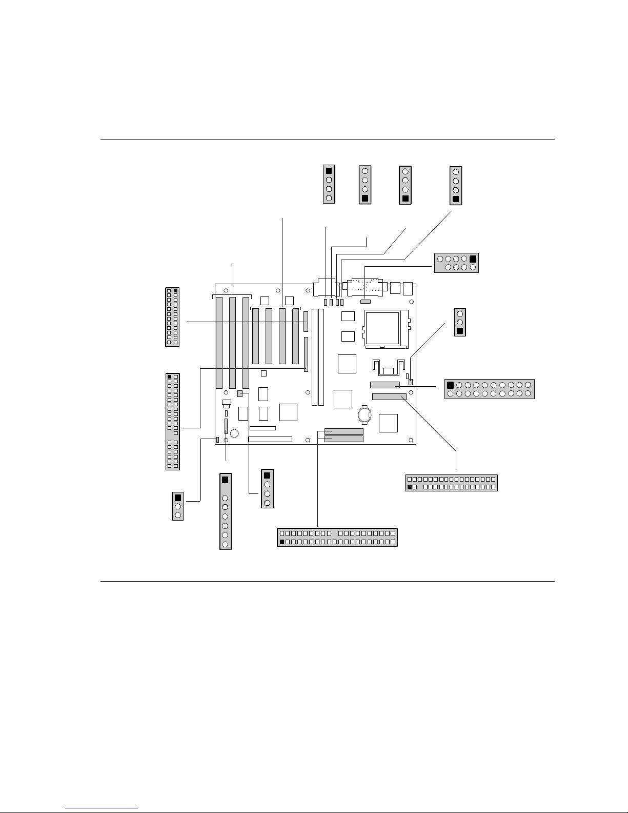
1.13 Jumper Settings
Figure 8 shows the location of jumper blocks on the motherboard.
J8A1
Normal/
Recovery
1
3
Motherboard Description
J6M1
1
STD/
VRE
3
A B C D
465
465
465
465
J9C1
321
321
321
321
OM06168
Figure 8. Jumper Locations
CAUTION
Do not move any of the jumpers with the power on. Always turn off the power and unplug the
power cord from the computer before changing jumpers.
41
Page 42

AN430TX Motherboard Technical Product Specification
Table 29. Jumper Settings
Function Jumper Configuration
Processor Voltage J6M1 1-2 Standard voltage
Password J9C1-A 1-2 Password enabled (Default)
CMOS (NVRAM and ESCD) Clear J9C1-A 4-5 Keep (Default)
BIOS Setup Access J9C1-B 1-2 Access enabled (Default)
Reserved J9C1-B 4-5 (Reserved)
Host Bus Frequency* J9C1-C See Table 30
Processor Frequency J9C1-D See Table 30
BIOS recovery J8A1 1-2 Normal (Default)
* These jumpers also set the PCI and ISA bus frequencies
2-3 VRE voltage (Default)
2-3 Password clear/disabled
5-6 Clear
2-3 Access denied
5-6 (Reserved)
2-3 Recovery
1.13.1 Processor Configuration (J9C1-C, D)
The motherboard must be configured for the frequency of the installed processor. Table 30 shows
the jumper settings for each frequency and the corresponding host bus, PCI bus, and ISA bus
frequencies.
Table 30. Jumper Settings for Processor and Bus Frequencies
Processor
Freq. (MHz)
200 5-6 1-2 and 5-6 66 33 8.33 3
166 5-6 2-3 and 5-6 66 33 8.33 2.5
150 4-5 2-3 and 5-6 60 30 7.5 2.5
133 5-6 2-3 and 4-5 66 33 8.33 2
120 4-5 2-3 and 4-5 60 30 7.5 2
100 5-6 1-2 and 4-5 66 33 8.33 1.5
90 4-5 1-2 and 4-5 60 30 7.5 1.5
NOTE
✏
There are no separate or additional jumpering requirements for Pentium processors with MMX
technology.
Jumpers
J9C1-C
Jumpers
J9C1-D
Host Bus
Freq. (MHz)
PCI Bus
Freq. (MHz)
ISA Bus
Freq. (MHz)
Bus/Processor
Freq. Ratio
42
Page 43

Motherboard Description
1.13.2 Password Clear (J9C1-A)
Use this jumper to clear the password if the password is forgotten. The default setting is pins 1-2
(password enabled). To clear the password, turn off the computer, move the jumper to pins 2-3,
and turn on the computer. Then, turn off the computer and return the jumper to pins 1-2 to restore
normal operation. If the jumper is in the 2-3 position (password disabled), you cannot set a
password.
1.13.3 Clear CMOS (J9C1-A)
This jumper resets the CMOS settings to the default values. This procedure must be done each
time the BIOS is updated. The default setting for this jumper is pins 4-5 (keep CMOS settings).
To reset the CMOS settings to the default values, turn off the computer, move the jumper to
pins 5-6, then turn on the computer. When the computer displays the message “NVRAM cleared
by jumper,” turn off the computer and return the jumper to pins 4-5 to restore normal operation.
1.13.4 BIOS Setup Access (J9C1-B)
This jumper enables or disables access to the Setup program. The default setting is pins 1-2
(access enabled). To disable access to the Setup program, move the jumper to pins 2-3.
1.13.5 BIOS Recovery (J8A1)
This jumper lets you recover the BIOS data from a diskette in the event of a catastrophic failure.
The default setting is pins 1-2 (normal operation). To recover the BIOS, turn off the computer,
move the jumper to pins 2-3, then turn on the computer to perform BIOS recovery. After recovery,
turn off the computer and return the jumper to pins 1-2 to restore normal operation. See
Section 3.1.12 for more details.
1.13.6 Processor Voltage (J6M1)
This jumper sets the output of the onboard voltage regulator. For processors that require Standard
voltage, place the jumper on pins 1-2. For processors that require VRE voltage, place the jumper
on pins 2-3. Voltage specifications are as follow:
• Standard = 3.3 - 3.465 V
• VRE = 3.465 - 3.63 V
CAUTION
When installing a processor in the motherboard for the first time or upgrading to a new processor,
check the processor’s documentation for the correct voltage setting. Operating the processor at
the wrong voltage can cause unreliable performance.
1.14 Reliability
The Mean-Time-Between-Failures (MTBF) data is calculated from predicted data at 55 oC.
Motherboard MTBF: 69,416 hours
43
Page 44

AN430TX Motherboard Technical Product Specification
1.15 Environmental
Table 31. Motherboard Environmental Specifications
Parameter Specification
Temperature
Non-Operating -40 oC to +70 oC
Operating 0 oC to +55 oC
Vibration
Unpackaged 5 Hz to 20 Hz : 0.01g² Hz sloping up to 0.02 g² Hz
20 Hz to 500 Hz : 0.02g² Hz (flat)
Packaged 10 Hz to 40 Hz : 0.015g² Hz (flat)
40 Hz to 500 Hz : 0.015g² Hz sloping down to 0.00015 g² Hz
1.16 Power Consumption
Tables 32 and 33 list voltage and current specifications for a computer that contains the
motherboard, a 200 MHz Pentium processor with MMX technology, 32 MB SDRAM, 256 KB
cache, 2 MB SGRAM graphics memory, a 3.5-inch floppy drive, a 1.6 GB hard drive, an 8X IDE
CD-ROM, and a 28.8 Kbps ISA faxmodem. This information is preliminary and is provided only
as a guide for calculating approximate power usage with additional resources added.
NOTE
✏
AC power measurements include all peripheral components mentioned above. DC current
measurements include only the motherboard components.
Table 32. DC Voltage
DC Voltage Acceptable Tolerance
+3.3 V ± 5%
+5 V ± 5%
-5 V ± 5%
+12 V ± 5%
-12 V ± 5%
Table 33. Power Usage for a static Windows 95 Desktop
APM Mode System AC (watts) Motherboard DC (amps)
APM disabled in BIOS 58 0.9 5.0 0.01 0.16 0.03
Maximum power savings 28 0.6 2.0 0.01 0.13 0.03
44
+3.3 V +5 V -5 V +12 V -12 V
Page 45

Motherboard Description
1.16.1 Power Supply Considerations
The motherboard is designed to operate with at least a 200 W ATX power supply for typical
configurations or a higher wattage supply for heavily loaded configurations. The power supply
must meet the following requirements:
• Rise time for power supply: 2 ms to 20 ms
• Minimum delay for Reset to Power Good: 100 ms
• Minimum Powerdown warning: 1 ms
• 3.3 V output must reach its minimum regulation level within ± 20 ms of the 5V output
reaching its minimum regulation level
1.17 Regulatory Compliance
This printed circuit assembly complies with the following safety and EMI regulations when
correctly installed in a compatible host system.
1.17.1 Safety
1.17.1.1 UL 1950 - CSA 950-95, 3rd edition, Dated 3-28-95
The Standard for Safety of Information Technology Equipment including Electrical Business
Equipment. (USA & Canada)
1.17.1.2 CSA C22.2 No. 950-93, 3rd Edition
The Standard for Safety of Information Technology Equipment including Electrical Business
Equipment. (Canada)
1.17.1.3 EN 60 950, 2nd Edition, 1992 (with Amendments 1, 2 & 3)
The Standard for Safety of Information Technology Equipment including Electrical Business
Equipment. (European Union)
1.17.1.4 IEC 950, 2nd edition, 1991 (with Amendments 1, 2 & 3)
The Standard for Safety of Information Technology Equipment including Electrical Business
Equipment. (International)
1.17.1.5 EMKO-TSE (74-SEC) 207/94
Summary of Nordic deviations to EN 60 950. (Norway, Sweden, Denmark & Finland)
45
Page 46

AN430TX Motherboard Technical Product Specification
1.17.2 EMI
1.17.2.1 FCC Class B
Title 47 of the Code of Federal Regulations, Parts 2 & 15, Subpart B, pertaining to unintentional
radiators. (USA)
1.17.2.2 CISPR 22, 2nd Edition, 1993
Limits and methods of measurement of Radio Interference Characteristics of Information
Technology Equipment. (International)
1.17.2.3 EN 55 022, 1995
Limits and methods of measurement of Radio Interference Characteristics of Information
Technology Equipment. (Europe)
1.17.2.4 EN 50 082-1 (1992)
Generic Immunity Standard; Currently compliance is determined via testing to IEC 801-2, -3 and
-4. (Europe)
1.17.2.5 VCCI Class 2 (ITE)
Implementation Regulations for Voluntary Control of Radio Interference by Data Processing
Equipment and Electronic Office Machines. (Japan)
1.17.2.6 ICES-003, Issue 2
Interference-Causing Equipment Standard, Digital Apparatus. (Canada)
1.17.3 Product Certification Markings
This printed circuit assembly has the following product certification markings:
• European CE Marking: Consists of a marking on the board or shipping container.
• UL Recognition Mark: Consists of the UL File No. E139761 on the component side of the
board and the PB No. on the solder side of the board. Board material flammability is 94V-1
or -0.
• Canadian Compliance: Consists of small c followed by a stylized backward UR on component
side of board.
46
Page 47

2 Motherboard Resources
NOTE
✏
For more detailed information about the resources used for onboard audio, see the Audio
Subsystem section in Chapter 1.
2.1 Memory Map
Table 34. Memory Map
Address Range
(decimal)
1024 K - 262144 K 100000 - 10000000 255 MB Extended Memory
960 K - 1024 K F0000 - FFFFF 64 K BIOS
944 K - 960 K EC000 - EFFFF 16 K Boot Block (available as UMB)
936 K - 944 K EA000 - EBFFF 8 K ESCD (Plug and Play configuration and
932 K - 936 K E9000 - E9FFF 4 K Reserved for BIOS
928 K - 932 K E8000 - E8FFF 4 K OEM Logo or Scan User Flash
896 K - 928 K E0000 - E7FFF 32 K POST BIOS (available as UMB)
800 - 896 K C8000 - DFFFF 96 K Available High DOS memory (open to ISA
640 K - 800 K A0000 - C7FFF 160 K Video memory and BIOS
639 K - 640 K 9FC00 - 9FFFF 1 K Extended BIOS data (movable by memory
512 K - 639 K 80000 - 9FBFF 127 K Extended conventional memory
0 K - 512 K 00000 - 7FFFF 512 K Conventional memory
2.2 DMA Channels
Table 35. DMA Channels
Address Range
(hex) Size Description
DMI)
and PCI bus)
manager software)
DMA Channel Number Data Width Resource
0 8- or 16-bits Audio
1 8- or 16-bits Audio / Parallel Port
2 8- or 16-bits Floppy Drive
3 8- or 16-bits ECP parallel port / Audio
4 Reserved - Cascade Channel
5 16-bits Open
6 16-bits Open
7 16-bits Open
47
Page 48

AN430TX Motherboard Technical Product Specification
2.3 I/O Map
Table 36. I/O Map
Address (hex) Size Description
0000 - 000F 16 bytes PIIX4 - DMA 1
0020 - 0021 2 bytes PIIX4 - Interrupt Controller 1
002E - 002F 2 bytes Super I/O Controller Configuration Registers
0040 - 0043 4 bytes PIIX4 - Counter/Timer 1
0048 - 004B 4 bytes PIIX4 - Counter/Timer 2
0060 1 byte Keyboard Controller Byte - Reset IRQ
0061 1 byte PIIX4 - NMI, Speaker Control
0064 1 byte Keyboard Controller, CMD/STAT Byte
0070, bit 7 1 bit PIIX4 - Enable NMI
0070, bits 6:0 7 bits PIIX4 - Real Time Clock, Address
0071 1 byte PIIX4 - Real Time Clock, Data
0078 1 byte Reserved - Board Configuration
0079 1 byte Reserved - Board Configuration
0081 - 008F 16 bytes PIIX4 - DMA Page Registers
00A0 - 00A1 2 bytes PIIX4 - Interrupt Controller 2
00B2 - 00B3 2 bytes APM Control
00C0 - 00DE 31 bytes PIIX4 - DMA 2
00F0 1 byte Reset Numeric Error
0170 - 0177 8 bytes Secondary IDE Channel
01F0 - 01F7 8 bytes Primary IDE Channel
0200 - 0207 8 bytes Audio / Game Port
0220 - 022F 16 bytes Audio (Sound Blaster compatible)
0240 - 024F 16 bytes Audio (Sound Blaster compatible)
0278 - 027F 8 bytes LPT2
02E8 - 02EF 8 bytes COM4 / Video (8514A)
02F8 - 02FF 8 bytes COM2
0300 - 0301 2 bytes MPU-401 (MIDI)
0330 - 0331 2 bytes MPU-401 (MIDI)
0332 - 0333 2 bytes MPU-401 (MIDI)
0334 - 0335 2 bytes MPU-401 (MIDI)
0376 1 byte Secondary IDE Channel Command Port
0377 1 byte Floppy Channel 2 Command
0377, bit 7 1 bit Floppy Disk Change, Channel 2
0377, bits 6:0 7 bits Secondary IDE Channel Status Port
0378 - 037F 8 bytes LPT1
0388- 038D 6 bytes AdLib (FM synthesizer)
48
continued ☛
Page 49

Table 36. I/O Map (continued)
Address (hex) Size Description
03B4 - 03B5 2 bytes Video (VGA)
03BA 1 byte Video (VGA)
03BC - 03BF 4 bytes LPT3
03C0 - 03CA 11 bytes Video (VGA)
03CC 1 byte Video (VGA)
03CE - 03CF 2 bytes Video (VGA)
03D4 - 03D5 2 bytes Video (VGA)
03DA 1 byte Video (VGA)
03E8 - 03EF 8 bytes COM3
03F0 - 03F5 6 bytes Floppy Channel 1
03F6 1 byte Primary IDE Channel Command Port
03F7 (Write) 1 byte Floppy Channel 1 Command
03F7, bit 7 1 bit Floppy Disk Change Channel 1
03F7, bits 6:0 7 bits Primary IDE Channel Status Port
03F8 - 03FF 8 bytes COM1
04D0 - 04D1 2 bytes Edge/level triggered PIC
0530 - 0537 8 bytes Windows Sound System
0604 - 060B 8 bytes Windows Sound System
LPTn + 400h 8 bytes ECP port, LPTn base address + 400h
0CF8 - 0CFB* 4 bytes PCI Configuration Address Register
0CF9** 1 byte Turbo and Reset Control Register
0CFC - 0CFF 4 bytes PCI Configuration Data Register
0E80 - 0E87 8 bytes Windows Sound System
0F40- 0F47 8 bytes Windows Sound System
0F86 - 0F87 2 bytes Yamaha OPL3-SA Configuration
FF00 - FF07 8 bytes IDE Bus Master Register
FFA0 - FFA7 8 bytes Primary Bus Master IDE Registers
FFA8 - FFAF 8 bytes Secondary Bus Master IDE Registers
Dynamically
allocated in PCI
I/O space
* DWORD access only
** Byte access only
32 bytes USB
Motherboard Resources
NOTE
✏
See the Audio section(s) in Chapter 1 for specific I/O addresses that can be used by the audio
components on your motherboard. This table does not list I/O addresses that may be used by addin cards in the computer.
49
Page 50

AN430TX Motherboard Technical Product Specification
2.4 PCI Configuration Space Map
Table 37. PCI Configuration Space Map
Bus
Number (hex)
00 00 00 Intel 82430TX (MTXC)
00 07 00 Intel 82430TX (PIIX4 ) PCI/ISA bridge, function 0
00 07 01 Intel 82430TX (PIIX4 ) IDE Bus Master, function 1
00 07 02 Intel 82430TX (PIIX4 ) USB, function 2
00 07 03 Intel 82430TX (PIIX4) Power Management, function 3
00 08 00 ATI VGA Graphics
00 0D 00 PCI Expansion Slot #1 (J4E2)
00 0E 00 PCI Expansion Slot #2 (J4E1)
00 0F 00 PCI Expansion Slot #3 (J4D1)
00 10 00 PCI Expansion Slot #4 (J4C1)
Device
Number (hex)
2.5 Interrupts
Table 38. Interrupts
IRQ System Resource
NMI I/O Channel Check
0 Reserved, Interval Timer
1 Reserved, Keyboard Buffer Full
2 Reserved, Cascade Interrupt From Slave PIC
3 COM2*
4 COM1*
5 LPT2 (Plug and Play option) / Audio / User available
6 Floppy Drive
7 LPT1*
8 Real Time Clock
9 User available
10 User available / USB
11 Windows Sound System* / User available
12 Onboard Mouse Port (if present, else user available)
13 Reserved, Math Coprocessor
14 Primary IDE (if present, else user available)
15 Secondary IDE (if present, else user available)
* Default, but can be changed to another IRQ
Function
Number (hex) Description
50
Page 51

Motherboard Resources
2.6 PCI Interrupt Routing Map
The PCI specification allows for sharing of interrupts between devices attached to the PCI bus. In
most cases, the small amount of latency added by interrupt sharing does not affect the normal
operation or throughput of the devices. However, in some special cases where maximum
performance is needed from a device, you may want to ensure that it does not share an interrupt
with other PCI devices.
This section describes the interrupt sharing mechanism and how the interrupt signals are connected
between the motherboard’s PCI expansion slots and onboard PCI devices. Use this information to
avoid sharing an interrupt for a PCI add-in card.
PCI devices are categorized as follows to specify their interrupt grouping:
• INTA: By default, all add-in cards that require only one interrupt are in this category. For
almost all cards that require more than one interrupt, the first interrupt on the card is also
classified as INTA.
• INTB: Generally, the second interrupt on add-in cards that require two or more interrupts is
classified as INTB. (This is not an absolute requirement.)
• INTC and INTD: Generally, a third interrupt on add-in cards is classified as INTC and a
fourth interrupt is classified as INTD.
The PIIX4 PCI-to-ISA bridge has four Programmable Interrupt Request (PIRQ) input signals. Any
PCI interrupt source (either onboard or from a PCI add-in card) connects to one of these PIRQ
signals. Because there are only four signals, some PCI interrupt sources are mechanically tied
together on the motherboard and therefore share the same interrupt. Table 39 lists the PIRQ
signals and shows how the signals are connected to the PCI expansion slots and to onboard PCI
interrupt sources.
Table 39. PCI Interrupt Routing Map
First PCI
PIIX4 PIRQ
Signal
PIRQA INTA INTD INTC INTB
PIRQB INTB INTA INTD INTC
PIRQC INTC INTB INTA INTD
PIRQD INTD INTC INTB INTA X X
Expansion
Slot: J4E2
Second PCI
Expansion
Slot: J4E1
Third PCI
Expansion
Slot: J4D1
Fourth PCI
Expansion
Slot: J4C1
Onboard
Video USB
For example, assume that you plug an add-in card that has one interrupt (group INTA) into the
fourth PCI slot. In this slot, an interrupt source from group INTA connects to the PIRQD signal,
which is already connected to the onboard video and USB PCI sources. The add-in card shares an
interrupt with these onboard interrupt sources. The PCI interrupts will dynamically configure an
available interrupt on the interrupt controller contained within the PIIX4.
51
Page 52

AN430TX Motherboard Technical Product Specification
Now, however, plug an add-in card that has one interrupt (group INTA) into the first PCI slot.
Plug a second add-in card that has two interrupts (groups INTA and INTB) into the second PCI
slot. INTA in the first slot is connected to signal PIRQA. INTA in the second slot is connected to
signal PIRQB, and INTB is connected to signal PIRQC. With no other cards added, the three
interrupt sources on the first two cards each have a PIRQ signal to themselves. Typically, they will
not share an interrupt.
NOTE
✏
The PIIX4 can connect each PIRQ line internally to one of the IRQ signals (3,4,5,7,9,11,14,15).
Typically, a device that does not share a PIRQ line will have a unique interrupt. However, in
certain interrupt-constrained situations, it is possible for two or more of the PIRQ lines to be
connected to the same IRQ signal.
52
Page 53

3 BIOS and Setup Program
3.1 Introduction
The motherboard uses an Intel BIOS, which is stored in Flash EEPROM and can be upgraded
using a floppy disk-based program. In addition to the BIOS, the Flash EEPROM contains the
Setup program, Power-On Self Tests (POST), advanced power management (APM), the PCI autoconfiguration utility, and Windows 95-ready Plug and Play. See Section 5.1 for the supported
versions of these specifications.
This motherboard supports BIOS shadowing, allowing the BIOS to execute from 64-bit onboard
write-protected DRAM.
The BIOS displays a sign-on message during POST identifying the type of BIOS and a revision
code. The initial production BIOS on the motherboard is identified as AN430TX0.86A.
3.1.1 BIOS Flash Memory Organization
The Intel PA28FB200BX 2 Mbit Flash component is organized as 256K x 8 (256 KB). The Flash
device is divided into areas as described in Table 40. The table shows the addresses in the ROM
image in normal mode (the addresses change in BIOS Recovery Mode).
Table 40. Flash Memory Organization
Address (Hex) Size Description
FFFF0000 - FFFFFFFF 64 KB Main BIOS *
FFFEC000 - FFFEFFFF 16 KB Boot Block
FFFEA000 - FFFEBFFF 8 KB Virtual Product Data (VPD) Extended System Configuration Data
(ESCD) (DMI configuration data / Plug and Play data)
FFFE9000 - FFFE9FFF 4 KB Used by BIOS (e.g., for Event Logging)
FFFE8000 - FFFE8FFF 4 KB OEM logo or Scan Flash Area
FFFC0000 - FFFE7FFF 160 KB Main BIOS Block
* At runtime, only this section is shadowed into RAM below the 1 MB address
53
Page 54

AN430TX Motherboard Technical Product Specification
3.1.2 BIOS Upgrades
Flash memory simplifies distributing BIOS upgrades. You can install a new version of the BIOS
from a diskette. BIOS upgrades are available to be downloaded from the secure section on the
Intel bulletin board or from Intel’s FTP or World Wide Web sites (see Section 5.2).
The disk-based Flash upgrade utility, IFLASH.EXE, has three options for BIOS upgrades:
• Update the Flash BIOS from a file on a disk
• Copy the current BIOS code from the Flash EEPROM to a disk file as a backup, in the event
that an upgrade cannot be successfully completed
• Compare the BIOS in the Flash device with a file to make sure the computer has the correct
version
The upgrade utility ensures that the upgrade BIOS extension matches the target computer to
prevent accidentally installing a BIOS for a different type of computer.
3.1.3 Plug and Play: PCI Auto-configuration
The PCI auto-configuration utility operates in conjunction with the Setup program to let you insert
and remove PCI cards without user configuration (Plug and Play). When you turn on the computer
after adding a PCI card, the BIOS automatically configures interrupts, I/O space, and other
parameters. Any interrupts set to “available” in Setup are considered free for use by PCI add-in
cards. PCI interrupts are distributed to available ISA interrupts that have been not been assigned to
an ISA card or to system resources. The assignment of PCI interrupts to ISA IRQs is
nondeterministic. An ISA device cannot share an interrupt allocated to PCI.
PCI configuration information is stored in ESCD format. You can clear the ESCD data by moving
the CMOS Clear jumper (see Section 1.13.3).
For information about the version of PCI and Plug and Play supported by this BIOS, see
Section 5.1. You can obtain copies of the specifications from the Intel World Wide Web site (see
Section 5.2). Peer-to-peer hierarchical PCI Bridge is supported, and by using an OEM-supplied
option ROM or TSR, a PCI-to-PCMCIA bridge capability is possible as well.
3.1.4 PCI IDE Support
If you select “Auto” in Setup, the BIOS automatically sets up the two local bus IDE connectors
with independent I/O channel support. The IDE interface supports hard drives up to PIO Mode 4
and recognizes any ATAPI devices, including CD-ROM drives and tape drives (see Section 5.1 for
the supported version of ATAPI). The BIOS determines the capabilities of each drive and
configures them to optimize capacity and performance. To take advantage of the high capacities
typically available today, hard drives are automatically configured for Logical Block Addressing
(LBA) and to PIO Mode 3 or 4, depending on the capability of the drive. You can override the
auto-configuration options by specifying manual configuration in Setup. The ATAPI Specification
recommends that ATAPI devices be configured as shown in Table 41.
54
Page 55

BIOS and Setup Program
Table 41. Recommendations for Configuring an ATAPI Device
Primary Cable Secondary Cable
Drive 0 Drive 1 Drive 0 Drive 1
Normal, no ATAPI ATA
Disk and CD-ROM for enhanced IDE systems ATA ATAPI
Legacy IDE System with only one cable ATA ATAPI
Enhanced IDE with CD-ROM and a tape or two CD-ROMs ATA ATAPI ATAPI
3.1.5 ISA Plug and Play
If you select in Setup to boot with a Plug and Play OS (see Section 3.2.4.1), the BIOS autoconfigures only ISA Plug and Play cards that are required for booting (IPL devices). If you select
to not boot with a Plug and Play OS, the BIOS auto-configures all Plug and Play ISA cards.
3.1.6 ISA Legacy Devices
Since ISA legacy devices are not auto-configurable, the resources for them must be reserved. You
can reserve resources in the Setup program or with an ISA configuration utility (see Section 5.2 for
a Web site address).
The computer’s configuration information is stored in ESCD format. You can clear the ESCD data
by moving the CMOS Clear jumper (see Section 1.13.3).
3.1.7 Desktop Management Interface
Desktop Management Interface (DMI) is a method of managing computers in an enterprise. The
main component of DMI is the Management Information Format (MIF) database, which contains
information about the computer and its components. Using DMI, a system administrator can
obtain the system types, capabilities, operational status, installation date and other information
about the computer’s components. The DMI specification requires that certain information about
the computer’s motherboard be made available to an applications program. This information is
located in a series of data structures which are accessed in various ways by the DMI service layer.
Component instrumentation allows the service layer to gain access to information stored in the
general-purpose area of non-volatile RAM. The MIF database defines the data and provides the
method for accessing the information.
The BIOS support for DMI enables the maximum benefit from applications such as LANDesk
Client Manager from Intel. The BIOS stores and can report on the following types of DMI
information:
• BIOS data, such as the BIOS revision level
• Fixed information, such as data about the motherboard, peripherals, serial numbers and asset
tags, etc.
• Information discovered during bootup, such as memory size, cache size, processor speed, etc.
• Dynamic information, such as event detection
55
Page 56

AN430TX Motherboard Technical Product Specification
An OEM can use a utility that makes DMI calls to program system and chassis-related information
into the Flash memory, so the BIOS can also report that information. Once this information is
written, it is locked (read-only).
Intel can provide a utility for making DMI calls to the BIOS. The latest DMI specification is
available from Intel (see Section 5.2) and other sites.
DMI does not work directly under non-Plug and Play operating systems (e.g., Windows NT).
However, the BIOS supports a DMI table interface for such OSs. Using this support, a DMI
service-level application running on a non-Plug and Play OS can access the DMI BIOS
information.
3.1.8 Advanced Power Management
The BIOS supports Advanced Power Management (APM); see Section 5.1 for the version
supported. You can initiate the energy saving Standby mode in two ways:
• Pressing the optional front panel Sleep/Resume button
• Prolonged inactivity; the timeout period is adjustable in the Setup program
When in Standby mode, the motherboard reduces power consumption by using the processor’s
System Management Mode (SMM) capabilities and by spinning down hard drives and reducing
power to or turning off VESA DPMS-compliant monitors. In Setup you can select the DPMS
mode to use for the monitor: Standby, Suspend, Sleep, or Disabled.
While in Standby mode, the computer retains the ability to respond to external interrupts; it can
service requests such as incoming faxes or network messages while unattended. Any keyboard or
mouse activity brings the computer out of Standby mode and immediately restores power to the
monitor.
APM is disabled in the BIOS by default; however, the computer must be configured with an
OS-dependent APM driver for the power-saving features to take effect. For example, Windows 95
enables APM automatically upon detecting the presence of the APM BIOS.
3.1.9 Language Support
The BIOS Setup program and help messages can be supported in 32 languages. Five languages are
available at this time: American English, German, Italian, French, and Spanish. The BIOS
includes extensions to support the Kanji character set and other non-ASCII character sets.
Translations of other languages may become available at a later date.
The default language is American English, which is always present unless another language is
programmed into the BIOS using the Flash Memory Update Program (IFLASH.EXE). See
Section 5.2 for information about downloading IFLASH and other utilities.
56
Page 57

BIOS and Setup Program
3.1.10 Boot Options
Booting from CD-ROM is supported in adherence to the “El Torito” bootable CD-ROM format
specification developed by Phoenix Technologies and IBM. Under the Boot Options field in
Setup, CD-ROM is one of four possible boot devices, which are defined in priority order. The
default settings are:
• First boot device - Removable devices (floppy drive)
• Second boot device - Hard drive
• Third boot device - CD-ROM
• Fourth boot device - Network
If you select CD-ROM as the boot device, it must be the first device.
NOTE
✏
A copy of the “El Torito” specification is available on the Phoenix Web site
http://www.ptltd.com/techs/specs.html.
In Setup you can also select the network as a boot device, which allows booting from a network
add-in card with a remote boot ROM installed.
3.1.11 OEM Logo or Scan Area
The motherboard supports a 4 KB programmable Flash user area at memory location
E8000-E8FFF. You can use this area to display a custom OEM logo during POST, or can insert a
binary image that executes at certain times during the POST. A utility is available from Intel to
assist with installing a logo into Flash for display during POST.
3.1.12 USB Support
The USB connector on the motherboard allows you to attach any of several USB devices as they
become available. Typically, the device driver for USB devices will be managed by the OS.
However, because keyboard and mouse support may be needed in the Setup program before the OS
boots, the BIOS supports USB legacy keyboards and mice. You can disable this support if
necessary.
3.1.13 BIOS Setup Access Jumper
You can move the Setup Access jumper on the motherboard to enable or disable access to the
Setup program. The default is for access to be enabled. See Section 1.13.4 for the specific pins on
which to place the jumper.
57
Page 58

AN430TX Motherboard Technical Product Specification
3.1.14 Recovering BIOS Data
Some types of failure can destroy the BIOS data. For example, the data could be lost if a power
outage occurs while your are updating the BIOS in Flash memory. You can recover the BIOS data
from a diskette by changing the setting of the BIOS Recovery jumper (see Section 1.13.5).
To create a BIOS recovery diskette, you must make a bootable DOS diskette and place the
recovery files on it. The recovery files are available from Intel.
To recover the BIOS, turn off the computer and move the jumper to the BIOS recovery setting.
Insert the bootable BIOS recovery diskette in drive A:. Boot the computer to recover the BIOS.
Two beeps and the end of floppy access to drive A: indicate a successful BIOS recovery. After a
successful recovery, turn off the computer by pressing the power switch for at least 4 seconds, and
return the jumper to the original pins to restore normal operation. A series of continuous beeps
indicates that the recovery operation failed.
NOTE
✏
No video is displayed during the recovery process.
3.2 BIOS Setup Program
The Setup program lets you modify the configuration for most basic changes without opening the
computer. Setup is accessible only during the Power-On Self Test (POST). To enter Setup, press
the <F2> key after the POST memory test has begun and before boot begins. See Section 1.13.4
for information on placing the jumper that prevents user access to Setup for security purposes.
3.2.1 Overview of the Setup Menu Screens
Table 42 lists the screens displayed by the Setup program. Setup initially displays the Main menu
screen. In each screen there are options for modifying the computer’s configuration. Select a
menu screen by pressing the left <←> or right <→> arrow keys. Use the up <↑> or down <↓>
arrow keys to select items in a screen. Use the <Enter> key to select a sub-menu. After you have
selected an item, use the <+> and <−> keys to modify the setting.
58
Page 59

BIOS and Setup Program
Table 42. Overview of the Setup Menu Screens
Setup Menu Screen Description
Main Set up and modify some of the basic options of a PC, such as time, date,
diskette drives, and hard drives.
Advanced Modify the more advanced features of a PC, such as peripheral configuration
and advanced chipset configuration.
Security Specify passwords that can be used to limit access to the computer.
Power Access and modify Power Management options.
Boot Modify options that affect boot up, such as the boot sequence.
Exit Save or discard changes.
Setup Subscreens Description
Floppy Options Used to configure diskette drive interface.
Primary IDE Master Used to configure the primary master IDE drive.
Primary IDE Slave Used to configure the primary slave IDE drive.
Secondary IDE Master Used to configure the secondary master IDE drive.
Secondary IDE Slave Used to configure the secondary slave IDE drive.
Resource Configuration Used to reserve memory blocks and specific IRQs.
Peripheral Configuration Used to configure peripherals.
Keyboard Configuration Used to configure keyboard options.
Video Configuration Used to configure onboard video resources.
DMI Event Logging View and modify DMI event logs.
Hard Drive Used to select hard drive.
Removable Devices Used to select removable devices.
3.2.2 Main Menu
3.2.2.1 Processor Type
Displays processor type.
3.2.2.2 Processor Speed
Displays processor speed.
3.2.2.3 Cache RAM
Displays size of L2 cache.
3.2.2.4 Total Memory
Displays the total amount of RAM on the motherboard.
3.2.2.5 BIOS Version
Displays the version of the BIOS.
59
Page 60

AN430TX Motherboard Technical Product Specification
3.2.2.6 Language
Selects the current default language used by the BIOS. The options are:
• English (US) (default)
• Italiano
• Français
• Deutsch
• Español
3.2.2.7 System Time
Specifies the current time.
3.2.2.8 System Date
Specifies the current date. Select the month, day, and year from a pop-up menu.
3.2.2.9 Floppy Options Submenu
When selected, this is used to configure the diskette drives.
3.2.2.9.1 Diskette A:
Specifies the capacity and physical size of diskette drive A:. The options are:
• Disabled
• 360 KB, 5.25 inch
• 1.2 MB, 5.25 inch
• 720 KB, 3.5 inch
• 1.44/1.25 MB, 3.5 inch (default)
• 2.88 MB, 3.5 inch
3.2.2.9.2 Diskette B:
Specifies the capacity and physical size of diskette drive B:. The options are:
• Disabled (default)
• 360 KB, 5.25 inch
• 1.2 MB, 5.25 inch
• 720 KB, 3.5 inch
• 1.44/1.25 MB, 3.5 inch
• 2.88 MB, 3.5 inch
3.2.2.9.3 Floppy Write Protect
Disables or enables write protect for the diskette drive(s). The options are:
• Disabled (default)
• Enabled
60
Page 61

BIOS and Setup Program
3.2.2.10 Primary IDE Master
Reports size of a connected IDE device. When selected, this displays the device configuration
subscreen for the Primary IDE master interface.
3.2.2.11 Primary IDE Slave
Reports size of a connected IDE device. When selected, this displays the device configuration
subscreen for the Primary IDE slave interface.
3.2.2.12 Secondary IDE Master
Reports size of a connected IDE device. When selected, this displays the device configuration
subscreen for the Secondary IDE master interface.
3.2.2.13 Secondary IDE Slave
Reports size of a connected IDE device. When selected, this displays the device configuration
subscreen for the Secondary IDE slave interface.
3.2.3 Primary/Secondary IDE Master/Slave Configuration Submenus
Used to manually configure the hard drive or have the computer automatically configure it.
3.2.3.1 Type
Selects the drive type that corresponds to the drive installed in your system. If set to User, the
number of Cylinders, Heads, and Sectors can be modified. The options are:
• None
• ATAPI Removable
• IDE Removable
• CD-ROM
• User
• Auto (default)
3.2.3.2 Cylinders
If device configuration is set to Auto, this field reports the number of cylinders for your hard disk
and cannot be modified. If IDE Device Configuration is set to User Definable, you must type the
correct number of cylinders for your hard disk.
3.2.3.3 Heads
If device configuration is set to Auto, this field reports the number of heads for your hard disk and
cannot be modified. If IDE Device Configuration is set to User Definable, you must type the
correct number of heads for your hard disk.
61
Page 62

AN430TX Motherboard Technical Product Specification
3.2.3.4 Sectors
If device configuration is set to Auto, this field reports the number of sectors for your hard disk and
cannot be modified. If IDE Device Configuration is set to User Definable, you must type the
correct number of sectors for your hard disk.
3.2.3.5 Maximum Capacity
Reports the maximum capacity of your hard disk, which is calculated from the number of
cylinders, heads, and sectors. There are no options.
3.2.3.6 Multi-Sector Transfers
Determines the number of sectors per block for multiple sector transfers. The options are:
• Disabled
• 2 Sectors
• 4 Sectors
• 8 Sectors
• 16 Sectors (default)
Check the specifications for your hard disk drive to determine which setting provides optimum
performance for your drive.
3.2.3.7 LBA Mode Control
Specifies the IDE translation mode. LBA causes logical block addressing to be used in place of
Cylinders, Heads, and Sectors. The options are:
• Disabled
• Enabled (default)
CAUTION
Do not change the IDE translation mode from the option selected when the hard drive was
formatted. Changing the option after formatting can result in corrupted data.
3.2.3.8 32 Bit I/O
Enables or disables 32 bit IDE data transfers. The options are:
• Disabled (default)
• Enabled
3.2.3.9 Transfer Mode
Sets how fast the transfers occur on the IDE interface. The options are:
• Standard
• Fast PIO 1
• Fast PIO 2
• Fast PIO 3
• Fast PIO 4 (default)
62
Page 63

3.2.3.10 Ultra DMA
Sets the Ultra DMA mode for the hard disk drive. The options are:
• Disabled (default)
• Mode 0
• Mode 1
• Mode 2
3.2.4 Advanced Menu
3.2.4.1 Plug & Play O/S
Select Yes if a Plug and Play operating system is being used. The options are:
• No
• Yes (default)
3.2.4.2 Reset Configuration Data
Used to clear the computer’s configuration data. The options are:
• No (default)
• Yes
BIOS and Setup Program
3.2.4.3 Memory Cache
The options are:
• Disabled
• Enabled (default)
3.2.4.4 Memory Bank 0
This status field reports the size and type of memory module in bank 0. There are no options.
3.2.4.5 Memory Bank 1
This status field reports the size and type of memory module in bank 1. There are no options.
3.2.4.6 Resource Configuration Submenu
3.2.4.6.1 Memory Reservation
Reserves specific upper memory blocks for use by legacy ISA devices. The options are:
• D000 - D3FF Available (default) | Reserved
• D400 - D7FF Available (default) | Reserved
• D800 - DBFF Available (default) | Reserved
• DC00 - DFFF Available (default) | Reserved
• Memory hole Disabled (default) | Conventional | Extended
63
Page 64

AN430TX Motherboard Technical Product Specification
3.2.4.6.2 IRQ Reservation
Reserve specific IRQs for use by legacy ISA devices. The options are:
• IRQ3 Available | Reserved
• IRQ4 Available | Reserved
• IRQ5 Available | Reserved
• IRQ7 Available | Reserved
• IRQ9 Available | Reserved
• IRQ10 Available | Reserved
• IRQ11 Available | Reserved
An * (asterisk) next to an IRQ indicates an IRQ conflict.
3.2.4.7 Peripheral Configuration Submenu
3.2.4.7.1 Serial Port A
Used to configure Serial Port A. The options are:
• Disabled
• Enabled
• Auto (Setup assigns the first free COM port, normally COM1, 3F8h, IRQ4) (default)
An * (asterisk) indicates a conflict with another device.
3.2.4.7.2 Serial Port B
Used to configure Serial Port B. The options are:
• Disabled
• Enabled
• Auto (Setup assigns the first free COM port, normally COM2, 2F8h, IRQ3) (default)
An * (asterisk) indicates a conflict with another device.
3.2.4.7.3 Mode
Sets the mode for Serial Port B: for normal (COM 2) or infrared applications. The options are:
• Normal (default)
• IrDA
• ASK-IR
3.2.4.7.4 Parallel Port
Used to configure the parallel port. The options are:
• Disabled
• Enabled
• Auto (Setup assigns LPT1, 378h, IRQ7) (default)
An * (asterisk) indicates a conflict with another device.
64
Page 65

3.2.4.7.5 Mode
Selects the mode for the parallel port. The options are:
• Output only (operates in AT
†
-compatible mode)
• Bi-directional (operates in bidirectional PS/2-compatible mode) (default)
• EPP (Extended Parallel Port, a high-speed bidirectional mode)
• ECP (Enhanced Capabilities, a high-speed bidirectional mode)
3.2.4.7.6 Floppy disk controller
Configures the floppy disk controller. The options are:
• Disabled
• Enabled (default)
3.2.4.7.7 IDE Controller
Configures the IDE controller. The options are:
• Disabled
• Primary
• Secondary
• Both (primary and secondary) (default)
BIOS and Setup Program
3.2.4.7.8 Audio
Enables or disables the onboard audio subsystem. The options are:
• Disabled
• Enabled (default)
3.2.4.8 Keyboard Features Submenu
3.2.4.8.1 Numlock
Sets the power on state of the Numlock feature on the numeric keypad of your keyboard. The
options are:
• Auto (default)
• On
• Off
3.2.4.8.2 Key Click
Enables the key click option. The options are:
• Disabled (default)
• Enabled
65
Page 66

AN430TX Motherboard Technical Product Specification
3.2.4.8.3 Keyboard Auto-repeat Rate
Selects the key repeat rate. The options are:
• 30/sec (default)
• 26.7/sec
• 21.8/sec
• 18.5/sec
• 13.3/sec
• 10/sec
• 6/sec
• 2/sec
3.2.4.8.4 Keyboard Auto-repeat Delay
Selects the delay before key repeat. The options are:
• ¼ sec
• ½ sec (default)
• ¾ sec
• 1 sec
3.2.4.9 Video Configuration Subscreen
3.2.4.9.1 Palette Snooping
Controls the ability of a primary PCI graphics controller to share a common palette with an ISA
add-in video card. The options are:
• Disabled (default)
• Enabled
3.2.4.9.2 Video Monitor Type
Selects the type of video monitor being used. (Available only with the ATI-ImpacTV option.) The
options are:
• VGA
• VGA and TV Out (default)
3.2.4.9.3 TV Out Signal Type
Selects the type of TV Out signal to be used. (Available only with the ATI-ImpacTV option.) The
options are:
• NTSC (North America) (default)
• PAL (Europe)
• PAL-M (South America)
66
Page 67

BIOS and Setup Program
3.2.4.10 DMI Event Logging Sub-menu
3.2.4.10.1 Event Log Capacity
Indicates if there is space available in the event log. There are no options.
3.2.4.10.2 Event Log Validity
Indicates if the contents of the event log are valid. There are no options.
3.2.4.10.3 View DMI event log
Enables viewing of DMI event log. Press <Enter> to view the event log. If there are no event logs
stored, the screen will read “No unread events”.
3.2.4.10.4 Clear all DMI event logs
Clears the DMI Event Log after rebooting. The options are:
• No (default)
• Yes
3.2.4.10.5 Event Logging
Enables Logging of DMI events. The options are:
• Disabled
• Enabled (default)
3.2.4.10.6 Mark DMI Events as read
Used to mark all DMI events as read. Press <Enter> to access the confirmation dialog box.
3.2.5 Security Menu
3.2.5.1 User Password Is
Reports if there is a User password set. There are no options.
3.2.5.2 Supervisor Password Is
Reports if there is a Supervisor password set. There are no options.
3.2.5.3 Set User Password
Sets the User password. The user will be asked to enter the new password and confirm the new
password. The password can be up to seven alphanumeric characters.
3.2.5.4 Set Supervisor Password
Sets the Supervisor password. The user will be asked to enter the new password and confirm the
new password. The password can be up to seven alphanumeric characters.
67
Page 68

AN430TX Motherboard Technical Product Specification
3.2.5.5 Unattended Start
When enabled, the computer will boot; however, if the computer is password protected, the
keyboard will be locked. Enter the user password to unlock the computer. The user password is
also required to boot from the floppy drive. The options are:
• Disabled (default)
• Enabled
3.2.6 Power Menu
3.2.6.1 Power Management
Enables or disables the BIOS Advanced Power Management feature. When set to disabled, fields
for Inactivity Timer, Hard Drive, and Video will not appear. The options are:
• Disabled (default)
• Enabled
3.2.6.2 Inactivity Timer
Sets the amount of time before the computer enters standby mode. The options are:
• Off (default)
• 1 Minute
• 2 Minutes
• 4 Minutes
• 6 Minutes
• 8 Minutes
• 12 Minutes
• 16 Minutes
3.2.6.3 Hard Drive
Enables the hard drive to be power managed during Standby and Suspend. The options are:
• Disabled
• Enabled (default)
3.2.6.4 Video
Enables video to be power managed during Standby and Suspend. The options are:
• Disabled
• Enabled (default)
3.2.7 Boot Menu
3.2.7.1 Scan User Flash Area
Allows BIOS to scan the flash memory for user binaries. The options are:
• Disabled (default)
• Enabled
68
Page 69

BIOS and Setup Program
3.2.7.2 First Boot Device
This status field reports the category of bootable device. The options are one (and only one) of the
following:
• Removable devices
• Hard Drive
• ATAPI CD-ROM devices
• Network boot
3.2.7.3 Second Boot Device
This status field reports the category of bootable device. The options are one (and only one) of the
following:
• Removable devices
• Hard Drive
• ATAPI CD-ROM devices
• Network boot
3.2.7.4 Third Boot Device
This status field reports the category of bootable device. The options are one (and only one) of the
following:
• Removable devices
• Hard Drive
• ATAPI CD-ROM devices
• Network boot
3.2.7.5 Fourth Boot Device
This status field reports the category of bootable device. The options are one (and only one) of the
following:
• Removable devices
• Hard Drive
• ATAPI CD-ROM devices
• Network boot
3.2.7.6 Hard Drive
This screen lists the available hard drive devices. The computer attempts to boot the operating
system from the first hard-drive in this list. If no operating system is found, the computer tries the
next drive listed until an operating system is found.
The options are any available hard drives. Press <Enter> for a list of available devices. To select
the boot device, use the up <↑> or down <↓> arrow keys. Press <+> to move the device up the
list, or <-> to move it down the list. Press <Esc> to exit this menu.
69
Page 70

AN430TX Motherboard Technical Product Specification
3.2.7.7 Removable Devices
This screen lists the available removable devices. The operating system assigns drive letters to
these devices in the order listed. You may change the sequence and therefore the drive lettering for
these devices by pressing the <+> or <-> keys.
The options are any available removable devices. Press <Enter> for a list of available devices. To
select the boot device, use the up <↑> or down <↓> arrow keys. Press <+> to move the device up
the list, or <-> to move it down the list. Press <Esc> to exit this menu.
3.2.8 Exit Menu
This section describes how to exit Setup with or without saving the changes you have made to
battery-backed CMOS RAM.
3.2.8.1 Exit Saving Changes
Exits Setup and saves the changes in CMOS RAM. You can also press the <F10> key anywhere
in the Setup program to do this.
3.2.8.2 Exit Discarding Changes
Exits Setup program without saving any changes. This means that any changes you have made
while in Setup are discarded and not saved. Pressing the <Esc> key in any of the four main screens
will also exit and discard changes.
3.2.8.3 Load Setup Defaults
Returns all of the Setup options to their defaults. The default Setup values are loaded from the
ROM table. You can also press the <F9> key anywhere in Setup to load the defaults.
3.2.8.4 Load Custom Defaults
Loads the setup settings from the Custom Defaults.
3.2.8.5 Save Custom Defaults
Normally, the BIOS reads the setup settings from battery backed CMOS RAM. If the CMOS
RAM fails, the BIOS uses the Custom Defaults (if you have set them). If no Custom Defaults are
set, the BIOS uses the factory defaults.
3.2.8.6 Discard Changes
Discards any changes made up to this point in Setup without exiting Setup. This selection loads
the CMOS RAM values that were present when the computer was turned on.
70
Page 71

4 Error Messages
4.1 BIOS Error Messages
Table 43. BIOS Error Messages
Error Message Explanation
Diskette drive A error or
Diskette drive B error
Extended RAM Failed at offset: nnnn Extended memory not working or not configured properly at offset
Failing Bits: nnnn The hex number nnnn is a map of the bits at the RAM address (in
Fixed Disk 0 Failure or
Fixed Disk 1 Failure or
Fixed Disk Controller Failure
Incorrect Drive A type - run SETUP Type of floppy drive A: not correctly identified in Setup.
Incorrect Drive B type - run SETUP Type of floppy drive B: not correctly identified in Setup.
Invalid NVRAM media type Problem with NVRAM (CMOS) access.
Keyboard controller error The keyboard controller failed test. Try replacing the keyboard.
Keyboard error Keyboard not working.
Keyboard error nn BIOS discovered a stuck key and displays the scan code nn for the
Keyboard locked - Unlock key switch Unlock the system to proceed.
Monitor type does not match CMOS -
Run SETUP
Operating system not found Operating system cannot be located on either drive A: or drive C:.
Parity Check 1 Parity error found in the system bus. BIOS attempts to locate the
Parity Check 2 Parity error found in the I/O bus. BIOS attempts to locate the
Press <F1> to resume, <F2> to
Setup
Drive A: or B: is present but fails the BIOS POST diskette tests.
Check to see that the drive is defined with the proper diskette type
in Setup and that the diskette drive is attached correctly.
nnnn.
System, Extended, or Shadow memory) which failed the memory
test. Each 1 (one) in the map indicates a failed bit.
Fixed disk is not working or not configured properly. Check to see
if fixed disk is attached properly. Run Setup be sure the fixed-disk
type is correctly identified.
stuck key.
Monitor type not correctly identified in Setup.
Enter Setup and see if fixed disk and drive A: are properly
identified.
address and display it on the screen. If it cannot locate the
address, it displays ????.
address and display it on the screen. If it cannot locate the
address, it displays ????.
Displayed after any recoverable error message. Press <F1> to
start the boot process or <F2> to enter Setup and change any
settings.
continued ☛
71
Page 72

AN430TX Motherboard Technical Product Specification
Table 43. BIOS Error Messages (continued)
Error Message Explanation
Previous boot incomplete - Default
configuration used
Real time clock error Real-time clock fails BIOS test. May require board repair.
Shadow Ram Failed at offset: nnnn Shadow RAM failed at offset nnnn of the 64k block at which the
System battery is dead - Replace and
run SETUP
System cache error - Cache disabled RAM cache failed the BIOS test. BIOS disabled the cache.
System CMOS checksum bad - run
SETUP
System RAM Failed at offset: nnnn System RAM failed at offset nnnn of in the 64k block at which the
System timer error The timer test failed. Requires repair of system board.
Previous POST did not complete successfully. POST loads default
values and offers to run Setup. If the failure was caused by
incorrect values and they are not corrected, the next boot will likely
fail. On systems with control of wait states, improper Setup settings
can also terminate POST and cause this error on the next boot.
Run Setup and verify that the wait-state configuration is correct.
This error is cleared the next time the system is booted.
error was detected.
The CMOS clock battery indicator shows the battery is dead.
Replace the battery and run Setup to reconfigure the system.
System CMOS has been corrupted or modified incorrectly, perhaps
by an application program that changes data stored in CMOS. Run
Setup and reconfigure the system either by getting the Default
Values and/or making your own selections.
error was detected.
4.2 Port 80h POST Codes
During POST (power-on self test), the BIOS generates diagnostic progress codes (POST codes) to
I/O port 80h. If the POST fails, execution stops and the last POST code generated is left at port
80h. This code is useful for determining the point where an error occurred.
Displaying the POST codes requires the use of an add-in card (often called a POST card). The
POST card can decode the port and display the contents on a medium such as a seven-segment
display. These cards can be purchased from JDR Microdevices or other sources.
The following table provides the POST codes that can be generated by the motherboard’s BIOS.
Some codes are repeated in the table because that code applies to more than one operation.
72
Page 73

Table 44. Port 80h Codes
Code Description of POST Operation Currently In Progress
02h Verify Real Mode
03h Disable Non-Maskable Interrupt (NMI)
04h Get CPU type
06h Initialize system hardware
08h Initialize chipset with initial POST values
09h Set IN POST flag
0Ah Initialize CPU registers
0Bh Enable CPU cache
0Ch Initialize caches to initial POST values
0Eh Initialize I/O component
0Fh Initialize the local bus IDE
10h Initialize Power Management
11h Load alternate registers with initial POST values
12h Restore CPU control word during warm boot
13h Initialize PCI Bus Mastering devices
14h Initialize keyboard controller
16h BIOS ROM checksum
17h Initialize cache before memory autosize
18h 8254 timer initialization
1Ah 8237 DMA controller initialization
1Ch Reset Programmable Interrupt Controller
20h Test DRAM refresh
22h Test 8742 Keyboard Controller
24h Set ES segment register to 4 GB
26h Enable A20 line
28h Autosize DRAM
29h Initialize POST Memory Manager
2Ah Clear 512 KB base RAM
2Ch RAM failure on address line
2Eh RAM failure on data bits
2Fh Enable cache before system BIOS shadow
30h RAM failure on data bits
32h Test CPU bus-clock frequency
33h Initialize POST Dispatch Manager
34h Test CMOS RAM
35h Initialize alternate chipset registers
36h Warm start shut down
37h Reinitialize the chipset (MB only)
xxxx
*
xxxx
* of low byte of memory bus
xxxx
* of high byte of memory bus
Error Messages
continued ☛
73
Page 74

AN430TX Motherboard Technical Product Specification
Table 44. Port 80h Codes (continued)
Code Description of POST Operation Currently In Progress
38h Shadow system BIOS ROM
39h Reinitialize the cache (MB only)
3Ah Autosize cache
3Ch Configure advanced chipset registers
3Dh Load alternate registers with CMOS values
40h Set Initial CPU speed new
42h Initialize interrupt vectors
44h Initialize BIOS interrupts
45h POST device initialization
46h Check ROM copyright notice
47h Initialize manager for PCI Option ROMs
(Rel. 5.1 and earlier)
48h Check video configuration against CMOS
49h Initialize PCI bus and devices
4Ah Initialize all video adapters in system
4Bh Display QuietBoot screen
4Ch Shadow video BIOS ROM
4Eh Display BIOS copyright notice
50h Display CPU type and speed
51h Initialize EISA board
52h Test keyboard
54h Set key click if enabled
56h Enable keyboard
58h Test for unexpected interrupts
59h Initialize POST display service
5Ah Display prompt "Press F2 to enter SETUP"
5Bh Disable CPU cache
5Ch Test RAM between 512 and 640 KB
60h Test extended memory
62h Test extended memory address lines
64h Jump to UserPatch1
66h Configure advanced cache registers
67h Initialize Multi Processor APIC
68h Enable external and CPU caches
69h Setup System Management Mode (SMM) area
6Ah Display external L2 cache size
6Ch Display shadow-area message
6Eh Display possible high address for UMB recovery
74
continued ☛
Page 75

Table 44. Port 80h Codes (continued)
Code Description of POST Operation Currently In Progress
70h Display error messages
72h Check for configuration errors
74h Test real-time clock
76h Check for keyboard errors
7Ah Test for key lock on
7Ch Set up hardware interrupt vectors
7Eh Initialize coprocessor if present
80h Disable onboard Super I/O ports and IRQs
81h Late POST device initialization
82h Detect and install external RS232 ports
83h Configure non-MCD IDE controllers
84h Detect and install external parallel ports
85h Initialize PC-compatible PnP ISA devices
86h Re-initialize onboard I/O ports
87h Configure Motherboard Configurable Devices
88h Initialize BIOS Data Area
89h Enable Non-Maskable Interrupts (NMIs)
8Ah Initialize Extended BIOS Data Area
8Bh Test and initialize PS/2 mouse
8Ch Initialize floppy controller
8Fh Determine number of ATA drives
90h Initialize hard-disk controllers
91h Initialize local-bus hard-disk controllers
92h Jump to UserPatch2
93h Build MPTABLE for multi-processor boards
94h Disable A20 address line (Rel. 5.1 and earlier)
95h Install CD-ROM for boot
96h Clear huge ES segment register
97h Fixup Multi Processor table
98h Search for option ROMs. One long, two short beeps on checksum failure
99h Check for SMART Drive
9Ah Shadow option ROMs
9Ch Set up Power Management
9Eh Enable hardware interrupts
9Fh Determine number of ATA and SCSI drives
A0h Set time of day
A2h Check key lock
A4h Initialize typematic rate
Error Messages
continued ☛
75
Page 76

AN430TX Motherboard Technical Product Specification
Table 44. Port 80h Codes (continued)
Code Description of POST Operation Currently In Progress
A8h Erase F2 prompt
AAh Scan for F2 key stroke
ACh Enter SETUP
AEh Clear IN POST flag
B0h Check for errors
B2h POST done - prepare to boot operating system
B4h One short beep before boot
B5h Terminate QuietBoot
B6h Check password (optional)
B8h Clear global descriptor table
B9h Clean up all graphics
BAh Initialize DMI parameters
BBh Initialize PnP Option ROMs
BCh Clear parity checkers
BDh Display MultiBoot menu
BEh Clear screen (optional)
BFh Check virus and backup reminders
C0h Try to boot with INT 19
C1h Initialize POST Error Manager (PEM)
C2h Initialize error logging
C3h Initialize error display function
C4h Initialize system error handler
The following are for boot block in Flash ROM
E0h Initialize the chipset
E1h Initialize the bridge
E2h Initialize the CPU
E3h Initialize system timer
E4h Initialize system I/O
E5h Check force recovery boot
E6h Checksum BIOS ROM
E7h Go to BIOS
E8h Set Huge Segment
E9h Initialize Multi Processor
EAh Initialize OEM special code
EBh Initialize PIC and DMA
ECh Initialize Memory type
EDh Initialize Memory size
76
continued ☛
Page 77

Table 44. Port 80h Codes (continued)
Code Description of POST Operation Currently In Progress
EEh Shadow Boot Block
EFh System memory test
F0h Initialize interrupt vectors
F1h Initialize Run Time Clock
F2h Initialize video
F3h Initialize beeper
F4h Initialize boot
F5h Clear Huge segment
F6h Boot to Mini DOS
F7h Boot to Full DOS
Error Messages
77
Page 78

Page 79

5 Specifications and Online Support
5.1 Specifications
The motherboard complies with the following specifications:
Table 45. Compliance with Specifications
Specification Description Revision Level
APM Advanced Power Management
BIOS interface specification
ATA-33 Synchronous DMA Transfer
Protocol specification (to be
proposed as Ultra DMA/33
standard)
ATX ATX form factor specification Revision 2.01, February 1997
DDC Display Data Channel standard Version 2, Revision 0, April 9, 1996
DMI Desktop Management Interface
BIOS specification
DPMS Display Power Management
Signaling
“El Torito” Bootable CD-ROM format
specification
EPP Enhanced Parallel Port IEEE 1284 standard, Mode [1 or 2]
Feature
Connector
IrDA Serial Infrared Physical Layer Link
PCI PCI Local Bus specification Revision 2.1, June 1, 1995
Plug and Play Plug and Play BIOS specification Version 1.0a, May 5, 1994
UHCI Universal Host Controller Interface Revision 1.0
USB Universal Serial Bus specification Revision 1.0, January 15, 1996
Advanced Feature Connector
(VAFC)
specification
Revision 1.2, February, 1996
Intel, Microsoft
Revision 0.7, May 21, 1996
Quantum document no. 70-108412-1
Video Electronics Standards Association
Version 2.0, October 16, 1995
American Megatrends Inc., Award Software
International Inc., Dell Computer Corporation, Intel,
Phoenix Technologies Ltd, SystemSoft Corporation
Revision 1.0
Video Electronics Standards Association
Version 1.0, January 25, 1995
Phoenix Technologies, IBM Corporation
Version 1.0, March 1994
Video Electronics Standards Association
Version 1.1, October 17, 1995
Infrared Data Association.
PCI Special Interest Group
Compaq Computer Corp, Phoenix Technologies, Intel
Compaq, Digital Equipment Corporation, IBM PC
Company, Intel, Microsoft, NEC, Northern Telecom
79
Page 80

AN430TX Motherboard Technical Product Specification
5.2 Online Support
Find information about Intel motherboards under “Product Info” or “Customer Support” at this
World Wide Web site:
http://www.intel.com/
or at this FTP site:
ftp://ftp.intel.com/pub/bios/
80
Page 81

Index
116450, 17
16550A, 17
A
AMI Megakey, 18
APM, 79
ATA-33, 79
ATI TractorBeam, 21
ATI-264GT Rage II+, 19
ATX, 79
B-C
battery, 18
BIOS, recovery jumper, 43
cache controller, 14
certification markings, 46
CISPR 22 compliance, 46
CSA compliance, 45
D
DDC2, 79
DMA controller, 15
DMI, 79
DPMS, 79
DRAM controller, 15
drivers, video capture, 21
E
ECP, 18
El Torito, 79
EMI regulations, 46
EMKO-TSE compliance, 45
EN 50 082-1 compliance, 46
EN 55 022 compliance, 46
EN 60 950 compliance, 45
EPP, 18, 79
error messages, port 80h codes, 72
expansion slots, 38
F
FCC compliance, 46
Feature Connector, 79
floppy drive controller, 18
form factor, 79
FTP site, 80
G-H
graphics controller, 19
heat sink, clips for, 12
hot key, 18
I
I/O controller, 17
I2C bus, 20
I2C connector, 37
ICES-003 compliance, 46
IDE interface, 15
IEC 950 compliance, 45
infrared, 19
interrupt controller, 15
interrupts, sharing PCI, 51
INTx PCI interrupt classification, 51
IrDA, 19, 79
ISA bus connectors, 39, 40
ISA Plug and Play, 17
J-M
jumpers, BIOS recovery, 43
keyboard interface, 18
mouse interface, 18
MPEG, 20
MTXC, 14
81
Page 82

AN430TX Motherboard Technical Product Specification
P
parallel port, 18
PC87307VUL, 17
PCI, 79
bus connectors, 38
bus interface, 15
expansion slots, 51
interrupt sharing, 51
PIIX4, 51
PIRQ signals, 51
Plug and Play, 79
port 80h codes, 72
POST (Power On Self Test), diagnostic
codes, 72
power management control, 15
product certification markings, 46
R-S
recovering BIOS data, 43
regulatory compliance, 45
safety regulations, 45
SECAM, 20
serial ports, 17
sharing interrupts, 51
slots for add-in cards, 38
specifications, 79
Super I/O controller, 17
S-Video, 21
S-video connector, 36, 37
T-U
TractorBeam, 21
TV-out, 21
UARTs, 17
UL compliance, 45
USB, 79
controller, 15
V-W
VCCI compliance, 46
VESA, 79
VESA connector, 20
video out, 21
video resolutions, 20
World Wide Web site, 80
82
 Loading...