

Page 1

21555 Non-Transparent PCI-toPCI Bridge
User Manual
July 2001
Order Number: 278321–002
Page 2

Information in this document is provided in connection with Intel® products. No license, express or implied, by estoppel or otherwise, to any intellectual
property rights is granted by this document. Except as provided in Intel’s Terms and Conditions of Sale for such products, Intel assumes no liability
whatsoever, and Intel disclaims any express or implied warranty, relating to sale and/or use of Intel products including liability or warranties relating to
fitness for a particular purpose, merchantability, or infringement of any patent, copyright or other intellectual property right. Intel products are not
intended for use in medical, life saving, or life sustaining applications.
Intel may make changes to specifications and product descriptions at any time, without notice.
Designers must not rely on the absence or characteristics of any features or instructions marked “reserved” or “undefined.” Intel reserves these for
future definition and shall have no responsibility whatsoever for conflicts or incompatibilities arising from future changes to the m.
The 21555 Non-Transparent PCI-to-PCI Bridge may contain design defects or errors known as errata which may cause the product to deviate from
published specifications. Current characterized errata are available on request.
This document and the software described in it are furnished under license and may only be used or copied in accordance with the terms of the
license. The i nf orm at i o n i n t h is do cum en t i s f ur n is he d f o r i nf o rm ati o na l u s e o nl y, is subject t o ch ang e w ith o ut n oti c e, an d s h ould not be construed as a
commitment by Intel Corporation. Intel Corporation assumes no responsibility or liability for any errors or inaccuracies that may appear in this
document or any software that may be provided in association with this document. Except as permitted by such license, no part of this document may
be reproduced, stored in a retrieval system, or transmitted in any form or by any means without the express written consent of Intel Corporation.
Contact your local Intel sales office or your distributor to obtain the latest specifications and before placing your product order.
Copies of documents which have an ordering number and are referenced in this document, or other Intel literature may be obtained by calling
1-800-548-4725 or by visiting Intel's website at http://www.intel.com.
Copyright © Intel Corporation, 2001
Intel is a trademark or registered trademark of Intel Corporation or its subsidiaries in the United States and other countries.
*Other names and brands may be cla imed as the property of others.
2 21555 Non-Transparent PC I-to-PCI Bridge User Manual
Page 3

Contents
Contents
1 Preface ..........................................................................................................................................11
1.1 Cautions and Notes ........................................................... ...... ....... ...... ....... ...... ....... ...... ....12
1.2 Data Units...........................................................................................................................12
1.3 Numbering ..........................................................................................................................12
1.4 Signal Nomenclature ..........................................................................................................13
1.5 Register Abbreviations........................................................................................................14
2 Introduction....................................................................................................................................15
2.1 Comparing a 21555 to a Transparent PPB.........................................................................15
2.2 Architectural Overview........................................................................................................18
2.2.1 Data Buffers...........................................................................................................18
2.2.2 Registers................................................................................................................18
2.2.3 Control Logic..........................................................................................................18
2.3 Special Applications............................................................................................................20
2.3.1 Primary Bus VGA Support.....................................................................................20
2.3.2 Secondary Bus VGA Support ................................................................................20
2.4 Programming Notes............................................................................................................20
2.4.1 Addressing.............................................................................................................20
2.4.2 Transaction Forwarding .........................................................................................21
2.4.3 ROM Access..........................................................................................................21
3 Signal Descriptions........................................................................................................................23
3.1 Primary PCI Bus Interface Signals .....................................................................................24
3.2 Primary PCI Bus Interface 64-Bit Extension Signals ..........................................................26
3.3 Secondary PCI Bus Interface Signals.................................................................................28
3.4 Secondary PCI Bus Interface 64-Bit Extension Signals .....................................................30
3.5 Miscellaneous Signals .......... ...... ....... ...... ....... ...... ...... ....................................... ....... ...... ... .31
4 Address Decoding .........................................................................................................................33
4.1 CSR Address Decoding......................................................................................................34
4.2 Expansion ROM Address Mapping (Decoding)..................................................................34
4.3 Memory 0 Transaction Address Decoding..........................................................................34
4.3.1 Using the BAR Setup Registers.............................................................................35
4.3.2 Direct Address Translation ....................................................................................36
4.3.3 Lookup Table Based Address Translation.............................................................37
4.3.4 Lookup Table Entry Format ...................................................................................40
4.3.5 Forwarding of 64-Bit Address Memory Transactions.............................................41
4.4 I/O Transaction Address Decoding.....................................................................................42
4.4.1 Indirect I/O Transaction Generation.......................................................................42
4.4.2 Subtractive Decoding of I/O Transactions ..... ....... ...... ....... ...... ....... .......................44
4.5 Configuration Accesses ......................................................................................................44
4.5.1 Type 0 Accesses to 21555 Configuration Space...................................................44
4.5.2 Initiation of Configuration Transactions by 21555..................................................45
4.6 21555 Bar Summary...... ....... ...... ....... ...... ....... ...... ....................................... ...... ....... ...... ....47
5 PCI Bus Transactions....................................................................................................................49
5.1 Transactions Overview .......................................................................................................49
21555 Non-Transparent PCI-to-PCI Bridge User Manual 3
Page 4

Contents
5.2 Posted Write Transactions ....... ...... ....... ...... ....... ...... ...... ....... ....................................... ...... .50
5.2.1 Memory Write Transactions...................................................................................51
5.2.2 Memory Write and Invalidate Transactions ....................................... ...... ....... ...... .51
5.2.3 64-bit Extension Posted Write Transaction............................................................52
5.2.4 Write Performance Tuning Options ............................................ ....... ...... ....... ...... .52
5.3 Delayed Write Transactions................................................................................................54
5.4 Delayed Read Transactions ...............................................................................................55
5.4.1 Nonprefetchable Reads.........................................................................................56
5.4.2 Prefetchable Reads ...............................................................................................57
5.4.3 Prefetchable Read Transactions Using the 64-bit Extension ................................57
5.4.4 Read Performance Features and Tuning Options.................................................57
5.5 64-Bit and 32-Bit Transactions Initiated by the 21555........................................................59
5.6 Target Terminations............................................................................................................60
5.6.1 Target Terminations Returned by the 21555.........................................................60
5.6.2 Transaction Termination Errors on the Target Bus................................................61
5.7 Ordering Rules....................................................................................................................61
6 Initialization Requirements ............................................................................................................65
6.1 Power Management, Hot-Swap, and Reset Signals...........................................................65
6.2 Reset Behavior ...................................................................................................................66
6.2.1 Central Function During Reset ..............................................................................68
6.3 21555 Initialization..............................................................................................................68
6.3.1 With SROM, Local, and Host Processors..............................................................69
6.3.2 Without Serial Preload................... ....... ...... ....................................... ...... ....... ...... .69
6.3.3 Without Local Processor... ....... ...... ....... ...... ...... ....... ...... ....... ...... ...........................70
6.3.4 Without Local Processor and Serial Preload .........................................................70
6.3.5 Without Host Processor........................ ...... ...... ....... ...... ....... .................................70
6.4 Power Management Support..............................................................................................70
6.4.1 Transitions Between Power Management States..................................................71
6.4.2 PME# Support .......................................................................................................71
6.4.3 Power Management Data Register................................ ....... ...... ....... ...... ....... ...... .72
6.5 CompactPCI Hot-Swap Functionality .................................................................................72
6.5.1 Overview of CompactPCI Controller Hardware Interface ......................................72
6.5.2 Insertion and Removal Process.............................................................................73
7 Clocking.........................................................................................................................................77
7.1 Primary and Secondary PCI Bus Clock Signals .................................................................77
7.2 21555 Secondary Clock Outputs........................................................................................78
7.3 66 MHz Support..................................................................................................................79
8 Parallel ROM Interface ..................................................................................................................81
8.1 Interface Signals.................................................................................................................81
8.2 Parallel and Serial ROM Connection..................................................................................84
8.3 PROM Read by CSR Access .............................................................................................84
8.4 PROM Write by CSR Access..............................................................................................86
8.5 PROM Dword Read............................................................................................................87
8.6 Access Time and Strobe Control........................................................................................88
8.7 Attaching Additional Devices to the ROM Interface............................................................89
9 Serial ROM Interface.....................................................................................................................91
9.1 SROM Interface Signals .....................................................................................................91
4 21555 Non-Transparent PC I-to-PCI Bridge User Manual
Page 5

Contents
9.2 SROMSROM Preload Operation........................................................................................91
9.3 SROM Configuration Data Preload Format ........................................................................92
9.4 SROM Operation by CSR Access ......................................................................................92
10 Arbitration ......................................................................................................................................97
10.1 Primary PCI Bus Arbitration Signals...................................................................................97
10.2 Secondary PCI Bus Arbitration Signals ..............................................................................97
10.3 Primary PCI Bus Arbitration................................................................................................98
10.4 Secondary PCI Bus Arbitration...........................................................................................98
10.4.1 Secondary Bus Arbitration Using the Internal Arbiter ............................................98
10.4.2 Secondary Bus Arbitration Using an External Arbiter..........................................100
11 Interrupt and Scratchpad Registers.............................................................................................101
11.1 Primary and Secondary PCI Bus Interrupt Signals...........................................................101
11.2 Interrupt Support...............................................................................................................101
11.3 Doorbell Interrupts ............................................................................................................103
11.4 Scratchpad Registers .......................................................................................................103
12 Error Handling .............................................................................................................................105
12.1 Error Signals.....................................................................................................................105
12.1.1 Primary PCI Bus Error Signals.............................................................................105
12.1.2 Secondary PCI Bus Error Signals........................................................................106
12.2 Parity Errors......................................................................................................................107
12.3 System Error (SERR#) Reporting.....................................................................................110
13 JTAG Test Port............................................................................................................................111
13.1 JTAG Signals....................................................................................................................111
13.2 Test Access Port Controller..............................................................................................112
13.2.1 Initialization..........................................................................................................112
14 I2O Support .................................................................................................................................113
14.1 Inbound Message Passing ...............................................................................................113
14.2 Outbound Message Passing.............................................................................................115
14.3 Notes ................................................................................................................................116
15 VPD Support................................................................................................................................119
15.1 Reading VPD Information .................................................................................................119
15.2 Writing VPD Information ...................................................................................................120
16 List of Registers........... ....... ...... ....... ...... ....... ...... ....... ...... ...... ....... ...... .........................................121
16.1 Register Summary............................................................................................................121
16.2 Configuration Registers ....................................................................................................122
16.3 Control and Status Registers............................................................................................126
16.4 Address Decoding ............................................................................................................130
16.4.1 Primary and Secondary Address ........................................................................130
16.4.2 Configuration Transaction Generation Registers.................................................140
16.5 PCI Registers....................................................................................................................147
16.5.1 Configuration Registers .......................................................................................147
16.5.2 Primary and Secondary Command Registers......................................................149
16.5.3 Device-Specific Control and Status Registers.....................................................156
16.6 I2O Registers....................................................................................................................165
21555 Non-Transparent PCI-to-PCI Bridge User Manual 5
Page 6

Contents
16.7 Interrupt Registers ............................................................................................................170
16.8 Scratchpad Registers . ...... ....... ...... ....... ...... ....... ...... ....................................... ...... ....... .....174
16.9 PROM Registers...............................................................................................................175
16.10 SROM Registers...............................................................................................................179
16.11 Arbiter Control............. ...... ....... ...... ....... ...... ....... ...... ...... ....... ...... ....... ...............................183
16.12 Error Registers..................................................................................................................183
16.13 Init Registers.....................................................................................................................185
16.14 JTAG Registers ................................................................................................................190
16.15 VPD Registers............................................ ....... ...... ...... ....... ...... ....... ...... ....... ...... ............192
Index .....................................................................................................................................................197
Figures
1 21555 Intelligent Controller Application......................................................................................16
2 21555 Microarchitecture .............................................................................................................19
3 BAR Setup Register Example ....................................................................................................35
4 Address Format..........................................................................................................................36
5 Direct Offset Address Translation...............................................................................................37
6 Downstream Address Translation Example ...............................................................................37
7 Address Translation Using A Lookup Table ...............................................................................39
8 Upstream Lookup Table Address Translation ............................................................................40
9 Lookup Table Entry Format ........................................................................................................41
10 Dual-Address Transaction Forwarding.......................................................................................42
11 CompactPCI Hot-Swap Connections .........................................................................................73
12 21555 Hot-Swap Insertion and Removal....................................................................................75
13 Synchronous Secondary Clock Generation................................................................................78
14 Parallel and Serial ROM Connections........................................................................................84
15 PROM Read Timing ...................................................................................................................85
16 PROM Write Timing....................................................................................................................87
17 Read and Write Strobe Timing ...................................................................................................88
18 Attaching Multiple Devices on the ROM Interface......................................................................90
19 SROM Write All Timing Diagram................................................................................................94
20 SROM Write Enable Timing Diagram.........................................................................................94
21 SROM Write Disable Timing Diagram........................................................................................94
24 SROM Check Status Timing Diagram........................................................................................95
22 SROM Erase Timing Diagram......... ...... ....... ...... ....... ...................................... ....... ...... ....... ...... .95
23 SROM Erase All Operation.........................................................................................................95
25 Secondary Arbiter Example........................................................................................................99
26 Signal trst_l States....................................................................................................................112
Tables
1 Signal Type Abbreviations..........................................................................................................13
2 Register Abbreviations ...............................................................................................................14
3 21555 and PPB Feature Comparison.........................................................................................17
4 Decoded and Not Decoded Addresses ......................................................................................20
5 Signal Pin Functional Groups.....................................................................................................23
6 Primary PCI Bus Interface Signals .............................................................................................24
6 21555 Non-Transparent PC I-to-PCI Bridge User Manual
Page 7

Contents
7 Primary PCI Bus Interface 64-Bit Extension Signals..................................................................26
8 Secondary PCI Bus Interface Signals.........................................................................................28
9 Secondary PCI Bus Interface 64-Bit Extension Signals .............................................................30
10 Miscellaneous Signals................................................................................................................31
11 Upstream Memory 2 Window Size ..... ....... ...... ....... ...... ...... ....... ...... ....... ...... ....... .......................38
12 Bar Summary..............................................................................................................................47
13 Delayed Write Transaction Target Termination Returns ............................................................55
14 Delayed Read Transaction Target Termination Returns............................................................56
15 Prefetch Boundaries ...................................................................................................................58
16 21555 Transaction Ordering Rules.............................................................................................62
17 Power Management, Hot-Swap, and Reset Signals...................................................................65
18 Reset Mechanisms .....................................................................................................................67
19 Power Management Actions.......................................................................................................71
20 Primary and Secondary PCI Bus Clock Signals.........................................................................77
21 PROM Interface Signals.............................................................................................................82
22 SROM Interface Signals.............................................................................................................91
23 Primary PCI Bus Arbitration Signals...........................................................................................97
24 Secondary PCI Bus Arbitration Signals ......................................................................................97
25 Arbiter Control Register............................................................................................................100
26 Primary and Secondary PCI Bus Interrupt Signals...................................................................101
27 Primary PCI Bus Error Signals .................................................................................................105
28 Secondary PCI Bus Arbitration Signals ....................................................................................106
29 Parity Error Responses.......... ....... ...... ....... ...... ....... ..................................................................107
30 JTAG Signals......................... ....... ...... ....... ...... ....................................... ...... ....... ...... .... ...........111
31 Register Cross Reference Table ..............................................................................................121
32 Configuration Space Address Register.....................................................................................122
33 CSR Address Map....................................................................................................................126
34 Primary CSR and Downstream Memory 0 Bar.........................................................................130
35 Secondary CSR Memory BARs................................................................................................131
36 Primary and Secondary CSR I/O Bars .....................................................................................132
37 Downstream I/O or Memory 1 and Upstream I/O or Memory 0 BAR........................................133
38 Downstream Memory 2 and 3 BAR, and Upstream Memory 1 BAR ........................................134
39 Upper 32 Bits Downstream Memory 3 Bar ...............................................................................135
40 Upstream Memory 2 Bar............... ...... ....... ...... ....... ...... ...... ....... ...............................................135
41 Downstream I/O or Memory 1 and Upstream I/O or Memory 0 Translated Base Register ......136
42 Downstream Memory 0, 2, 3, and Upstream Memory 1 Translated Base Register .................137
43 Downstream I/O or Memory 1 and Upstream I/O or Memory 0 Setup Registers .....................138
44 Downstream Memory 0, 2, 3, and Upstream Memory 1 Setup Registers ................................139
45 Upper 32 Bits Downstream Memory 3 Setup Register.............................................................140
46 Downstream and Upstream Configuration Address Registers.................................................141
47 Downstream Configuration Data and Upstream Configuration Data Registers........................142
48 Configuration Own Bits Register...............................................................................................142
49 Configuration CSR....................................................................................................................143
50 Downstream I/O Address and Upstream I/O Address Registers..............................................144
51 Downstream I/O Data and Upstream I/O Data Registers.........................................................145
52 I/O Own Bits Registers .............................................................................................................145
53 I/O CSR ....................................................................................................................................146
54 Lookup Table Offset Register...................................................................................................146
55 Lookup Table Data Register.....................................................................................................147
56 Upstream Memory 2 Lookup Table .... ....... ...... ....... ...... ...... ....... ...... ....... ..................................147
21555 Non-Transparent PCI-to-PCI Bridge User Manual 7
Page 8

Contents
57 Primary Interface Configuration Space Address Map ..............................................................148
58 Secondary Interface Configuration Space Address Map..........................................................148
59 Vendor ID Register...................................................................................................................148
60 Device ID Register....................................................................................................................148
61 Primary and Secondary Command Registers ..........................................................................149
62 Primary and Secondary Status Registers.................................................................................150
63 Revision ID (Rev ID) Register ..................................................................................................151
64 Primary and Secondary Class Code Registers ........................................................................152
65 Primary and Secondary Cache Line Size Registers.................................................................152
66 Primary Latency and Secondary Master Latency Timer Registers ..........................................153
67 Header Type Register ..............................................................................................................153
68 BiST Register ...........................................................................................................................153
69 Subsystem Vendor ID Register ................................................................................................154
70 Subsystem ID Register.............................................................................................................154
71 Enhanced Capabilities Pointe r Regis ter ....................................... ...... ....... ...... ....... ...... ............154
72 Primary and Secondary Interrupt Line Registers......................................................................154
73 Primary and Secondary Interrupt Pin Registers .......................................................................155
74 Primary and Secondary Minimum Grant Registers..................................................................155
75 Primary and Secondary Maximum Latency Registers..............................................................155
76 Device-Specific Control and Status Address Map....................................................................156
77 Chip Control 0 Register ............................................................................................................156
78 Chip Control 1 Register ............................................................................................................160
79 Chip Status Register.................................................................................................................162
80 Generic Own Bits Register .......................................................................................................164
81 I2O Outbound Post_List Status................................................................................................165
82 I2O Outbound Post_List Interrupt Mask ...................................................................................165
83 I2O Inbound Post_List Status...................................................................................................165
84 I2O Inbound Post_List Interrupt Mask......................................................................................166
85 I2O Inbound Queue..................................................................................................................166
86 I2O Outbound Queue ...............................................................................................................166
87 I2O Inbound Free_List Head Pointer........................................................................................167
88 I2O Inbound Post_List Tail Pointer...........................................................................................167
89 I2O Outbound Free_List Tail Pointer........................................................................................167
90 I2O Outbound Post_List Head Pointer .....................................................................................167
91 I2O Inbound Post_List Counter ................................................................................................168
92 I2O Inbound Free_List Counter................................................................................................168
93 I2O Outbound Post_List Counter .............................................................................................169
94 I2O Outbound Free_List Counter .............................................................................................169
95 Chip Status CSR ......................................................................................................................170
96 Chip Set IRQ Mask Register ....................................................................................................170
97 Chip Clear IRQ Mask Register .................................................................................................171
98 Upstream Page Boundary IRQ 0 Register ...............................................................................171
99 Upstream Page Boundary IRQ 1 Register ...............................................................................172
100 Upstream Page Boundary IRQ Mask 0 Register......................................................................172
101 Upstream Page Boundary IRQ Mask 1 Register......................................................................172
102 Primary Clear IRQ and Secondary Clear IRQ Registers..........................................................173
103 Primary Set IRQ and Secondary Set IRQ Registers ................................................................173
104 Primary Clear IRQ Mask and Secondary Clear IRQ Mask Registers.......................................174
105 Primary Set IRQ Mask and Secondary Set IRQ Mask Registers.............................................174
106 Scratchpad 0 Through Scratchpad 7 Registers........................................................................174
8 21555 Non-Transparent PC I-to-PCI Bridge User Manual
Page 9

Contents
107 Primary Expansion ROM BAR..................................................................................................175
108 Primary Expansion ROM Setup Register .................................................................................176
109 ROM Setup Register.................................................................................................................177
110 ROM Data Register ..................................................................................................................177
111 ROM Address Register.............................................................................................................178
112 ROM Control Register ..............................................................................................................178
113 Mode Setting Configuration Register........................................................................................179
114 Serial Preload Sequence.............. ...................................... ....... ...... ....... ...... ....... ...... ....... ........180
115 Arbiter Control Register............................................................................................................183
116 Primary SERR# Disable Register.............................................................................................184
117 Secondary SERR# Disable Register........................................................................................184
118 Power Management ECP ID and Next Pointer Register ..........................................................185
119 Power Management Capabilities Register................................................................................186
120 Power Management Control and Status Register ....................................................................187
121 PMCSR Bridge Support Extensions.........................................................................................187
122 Power Management Data Register...........................................................................................188
123 Reset Control Register .............................................................................................................188
124 CompactPCI Hot-Swap Capability Identifier and Next Pointer Register...................................189
125 CompactPCI Hot-Swap Control Register..................................................................................189
126 JTAG Instruction Register Options...........................................................................................190
127 Bypass Register........................................................................................................................191
128 Boundary-Scan Register.. ...... ....... ...... ....... ...... ....... ...................................... ....... ...... ....... ........191
129 Boundary Scan Order...............................................................................................................191
130 Vital Product Data (VPD) ECP ID and Next Pointer Register...................................................192
131 Vital Product Data (VPD) Address Register .............................................................................193
132 VPD Data Register ...................................................................................................................193
21555 Non-Transparent PCI-to-PCI Bridge User Manual 9
Page 10

Page 11

Preface 1
A brief description of the contents of this manual follows.
Chapter 1, “Preface” Provides information about the contents and organization of this book.
Chapter 2, “Introduction” Provides an overview of the 21555 functionality and architecture.
Chapter 3, “Signal Descriptions” Describes PCI signal pins grouped by function.
Chapter 4, “Address Decoding” Contains details about how addresses are decoded.
Chapter 5, “PCI Bus Transactions”
Chapter 6, “Initialization
Requirements”
Chapter 7, “Clocking” Describes 21555 clocking support.
Chapter 8, “Parallel ROM
Interface”
Chapter 9, “Serial ROM Interface” Describes the 21555 Serial ROM Interface.
Chapter 10, “Arbitration”
Chapter 11, “Interrupt and
Scratchpad Registers”
Chapter 12, “Error Handling” Describes parity error responses and system error reporting.
Chapter 13, “JTAG Test Port” Explains the implementation of JTAG test port.
Chapter 14, “I2O Support” Explains how the 21555 implements an I20 messaging unit.
Chapter 15, “VPD Support” Describes Vital Product Data support through SROM interface.
Chapter 16, “List of Registers”
Appendix A, “Acronyms” Definition of terms used in this book.
Describes how the 21555 implements
transactions.
Describes the reset operation and initialization requirements.
Describes the 21555 Parallel ROM Interface.
Explains how 21555 implements primary and secondary PCI bus
arbitration.
Describes interrupt support and scratchpad registers.
This chapter contains all of the 21555 register information and contains
a register summary.
the theory of operation about PCI
21555 Non-Transparent PCI-to-PCI Bridge User Manual 11
Page 12

Preface
1.1 Cautions and Notes
Caution: Cautions provid e in for mat ion to prevent damage to equipment or loss of data.
Note: Notes emphasize particularly important info rmation.
1.2 Data Units
This manual uses the following data-unit terminology.
Term Words Bytes Bits
Byte ½ 18
Word 1 2 16
Dword 2 4 32
Quadword 4 8 64
1.3 Numbering
All numbers are decimal unless appended with a radix specifier.
• “h” is the hexadecimal radix.
• “b” is the binary radix.
A range of (numbers, bits, bytes, addresses and so on) within a larger group of numbers is specified with colon (:).
The range may be enclosed in [square brackets] as well.
• The left number is upper limit of the range.
• The right number is the lower limit of the range.
For example: Primary byte offset: 13:10h.
12 21555 Non-Transparent PCI-to-PCI Bridge Use r Manual
Page 13

Preface
1.4 Signal Nomenclature
21555 device signal names are printed in lowercase typ e. Prefixes and s uffixes are tagged with a leading or trailing
letter and are delimited with an “_” underscore:
• The prefix “p_” denotes a primary bus signal. F or example: p_ad is the primary interface address/data bus.
• The prefix “s_” denotes a secondary bus signal. For example: s_ad is the secondary interface address/data bus.
• Other prefixes might appear. l_(load), pr_(parallel rom), and so on.
• The suffix “_l” means that the condition is qualified when that signal is low or approximately zero (0) volts.
For example: p_frame_l is a low-asserted signal.
• If no suffix is applied, it means that the condition is qualified when the signal is high or approximately equal to
vcc. For example: p_idsel is a high-asserted signal.
PCI signals that can be on either the primary interface or the secondary interface are printed in uppercase, normal
type. The names of low-asserted signals are followed by #. For example, “asserting FRAME#” can refer to the
assertion of the p_frame_l signal when the transaction is occurring on the primary bus or the assertion of the
s_frame_l signal when the transaction is occurring on the secondary bus.
Table 1 describes the Signal Type letter s th at ap pear in Table 6 through Table 10 in Chapter 3, “Signal
Descriptions”.
Table 1. Signal Type Abbreviations
Signal
Type
I Standard input only.
O Standard output only.
TS Tristate bidirectional.
STS
OD Standard open drain.
Description
Sustained tristate. Active low signal must be pulled high for one clock
cycle when deasserting.
21555 Non-Transparent PCI-to-PCI Bridge User Manual 13
Page 14

Preface
1.5 Register Abbreviations
When a register is associated with the primary interface, its name is preceded with Primary. When a register is
associated with the secondary interface, its name is preceded with Secondary. When a register is shared by both
interfaces, it is not preceded with Primary or Secondary. The byte offsets at which each register can be accessed
from each interface are listed in each register description.
Table 2 lists the register access abbreviations.
Table 2. Register Abbreviations
Access Type Description
DCA Downstream configuration address.
DCD Downstream configuration data.
DIA Downstream I/O address.
DID Downstream I/O data
R Read only. Writes have no effect.
R/W Read/Write.
R/W1TC Read. Write 1 to clear.
R/W1TS Read. Write 1 to set.
R0TS Read 0 to set.
R/(WS) Read. Write from secondary interface only. Primary bus writes have no effect.
R/(WP) Read. Write from primary interface only. Secondary bus writes have no effect.
UCA Upstream configuration address.
UCD Upstream configuration data.
UIA Upstream I/O address.
UID Upstream I/O data .
W1TL Write 1 to load.
14 21555 Non-Transparent PCI-to-PCI Bridge Use r Manual
Page 15

Introduction 2
The Intel® 21555 is a PCI peripheral devi ce t hat perf orm s P CI bridg i ng f unct ion s f or em bedd ed and i ntel lig ent I/O
applications. The 21555 has a 64-bit primary interface, a 64-bit secondary interface, and 66-MHz capability. In this
document the 21555 non-transparent device is compared to the related 21154 transparent devices. Both devices
have similar operating characteristic.
The 21555 is a “non-transparent” PCI-to-PCI Bridge (PPB) that acts as a gateway to an intelligent subsystem. It
allows a local processor to independently configu re and contr ol the local s ubsy stem. The 2 155 5 imp lem ents an I2 0
message unit that enables any local processor to function as an intelligent I/O processor (IOP) in an I20-capable
system. Since the 21555 is architecture independent, it works with any ho st an d local p rocess ors that s upp ort a PCI
bus. This architecture independence enables vendors to leverage existing investments while moving products to
PCI technology.
Unlike a transparent PPB, the 21555 is specifically designed to bridge between two processor domains. The
processor domain on the primary interface of the 21555 is referred to as the host domain, and its processor is the
host processor. The secondary bus interfaces to the local domain and the local processor. Special features include
support of:
• Independent primary and secondary PCI clocks. See Chapter 7.
• Independent primary and secondary address spaces.
• Address translation between the primary (host) and secondary (local) domains. See Chapter 4.
The 21555 allows add-in card vendors to pres ent a higher level of abstraction to the host system than is possible
with a transparent PPB. The 21555 uses a Type 0 configuration header, which presents the entire subsystem as a
single “device” to the host processor. This allows loading of a single device driver for the entire subsystem, and
independent local processor initialization and control of the subsystem devices. Since the 21555 uses a Typ e 0
configuration header, it does not require hierarchical PPB configuration code.
The 21555 forwards transactions between the primary and secondary PCI buses as does a transparent PPB. In
contrast to a transparent PPB, the 21555 can translate th e add ress o f a f orward ed tr ansa ction fr om a sy stem addr ess
to a local address, or vice versa. This mechanism allows the 21555 to hide subsystem resour ces from the host
processor and to resolve any resource conflicts that may exist between the host and local subsystems.
The 21555 operates at 3.3 V, but is also 5.0 -V I/ O to lera nt. A dap ter cards des i gned for th e 215 55 can be keyed as a
PCI universal card edge connector, permitting use in either a 5-V or 3-V slot.
2.1 Comparing a 21555 to a Transparent PPB
The 21555 is functionally similar to a transparent PPB in that both provide a connection path between devices
attached to two independent PC I buses. A 21555 and a PPB allow the electrical loading of devices on one PCI bus
to be isolated from the other bus while permitting concurrent operation on both buses. Since the PCI Local Bus
Specification restricts PCI option cards to a single electrical load, the ability of PPBs and the 21555 to spawn PCI
buses enables the design of multi-device PCI option cards. The key difference between a PPB and the 21555 is that
the presence of a PPB in a connection path between the host processor and a device is transparent to devices and
device drivers, while the presence of the 21555 is not. This difference enables the 21555 to provide features that
better support the use of intelligent controllers in the subsystem.
21555 Non-Transparent PCI-to-PCI Bridge User Manual 15
Page 16
Introduction
A primary goal of the PPB architecture is that PPB are transparent to devices and device drivers. For example, no
changes are needed to a device driver when a PCI peripheral is located behind a PPB. Once configured during
system initialization, a PPB operates without the aid of a device driver. A PPB does not require a device driver of its
own since it does not have any resources that must be managed by software dur ing run-time. This requirement for
transparency forced the usage of a flat addressing model across PPBs. This means that a given physical address
exists at only one location in the PCI bus hierarchy and that this location may be accessed by any d evice attached at
any point in the PCI bus hierarchy. As a consequence, it is not possible for a PPB to isolate devices or address
ranges from access by devices on the opposite interface of a PPB. The PPB architecture assumes that the resources
of any device in a PCI system are configured and managed by the host processor.
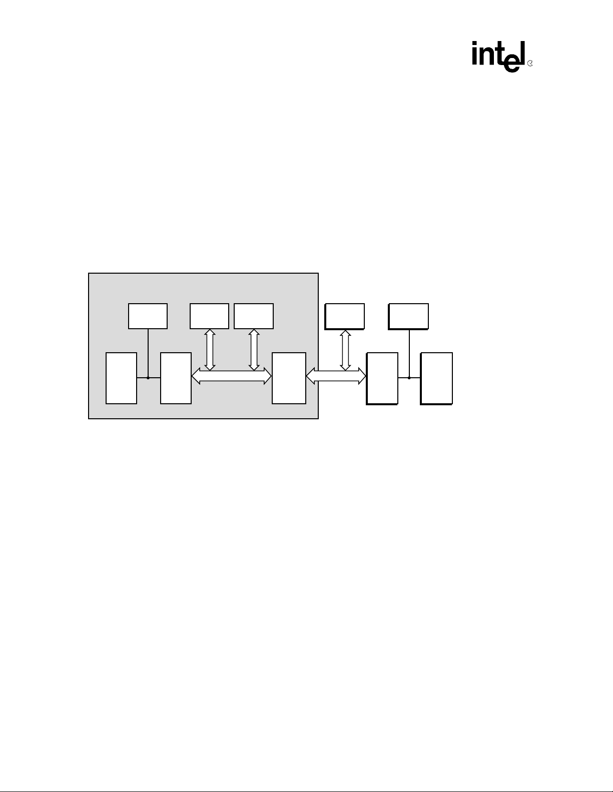
Figure 1 shows a hypothetical PCI add-in card used for an intelligent controller application. In some applications
the transparency of a PPB is not desired. For example,
Figure 1. 21555 Intelligent Controller Application
Intelligent Subsystem
Local
CPU
DRAM/
ROM
CPU-
PCI
Bridge
PCI
Device
PCI Bus
PCI
Device
Intel
21555
Device
PCI
Device
®
PCI Bus
Host
Core
Logic
Memory
Host
CPU
A8826-01
Assume:
• That the local processor on the add-in card is used to manage the resources of the devices attached to the add- in
card’s local PCI bus.
• That it is desirable to restrict access to these same resources from other PCI bus masters in the system and from
the host processor.
• That there is a need to resolve address conflicts that may exist between the hos t system and the local processor.
The non transparency of the 21555 is perfectly suited to this kind of configuratio n, where a transpar ent PPB woul d
be problematic.
Since the 21555 is non transparent, the device driver for the add-in card must be aware of the pres ence of the 21555
and manage its resources appropriately. The 21555 allows the entire subsystem to appear as a single virtual device
to the host. This enables configuration software to identify the appropriate driver for the subsystem.
With a transparent PPB, a driver does not need to know about the presence of the bridge and manage its resources.
The subsystem appears to the host system as individual PCI devices on a secondary PCI bus, not as a single virtual
device.
16 21555 Non-Transparent PCI-to-PCI Bridge Use r Manual
Page 17

Table 3 shows compares a 21555 and to a transparent PPB.
T a ble 3. 21555 and PPB Feature Comparison
Feature Non-Transparent PPB or 21555 Transparent PPB
Introduction
Transaction
forwarding
Address decoding
Address
translation
Configuration
-time resources
Run
Clocks
Secondary bus
central functions
• Adheres to PPB ordering rules.
• Uses posted writes and delayed
transactions.
• Adheres to PPB transaction error
and parity error guidelines,
although some errors may be
reported differently .
• Base address registers (BARs)
are used to define independent
downstream and upstream
forwarding windows.
• Inverse decoding is only used for
upstream transactions above the
4GB boundary.
Supported for both memory and I/O
transactions.
• Downstream devices are not
visible to host.
• Does not require hierarchical
configuration code (Type 0
configuration header).
• Does not respond to Type 1
configuration transactions.
• Supports configuration access
from the secondary bus.
• Implements separate set of
configuration registers for the
secondary interface.
Includes features such as doorbell
interrupts, I20 message unit, and so
on, that must be managed by the
device driver.
Generates secondary bus clock
output.
Asynchronous secondary clock input
is also supported.
Implements secondary bus arbiter.
This function can be disabled.
Drives secondary bus AD, C/BE#,
and PAR during reset. This function
can be disabled.
• Adheres to PPB ordering rules.
• Uses posted writes and delayed
transactions.
• Adheres to PPB transaction error and
parity error guidelines.
• PPB base and limit address registers are
used to define downstream forwarding
windows.
• Inverse decoding for upstream
forwarding.
None. Flat address model is assumed.
• Downstream devices are visible to host.
• Requires hierarchical configuration code
(Type 1 configuration header).
• Forwards and converts Type 1
configuration transactions.
• Does not support configuration access
from the secondary bus. Same set of
configuration registers is used to control
both primary and secondary interfaces.
Typically has only configuration registers; no
device driver is required.
Generates one or more secondary bus clock
outputs.
Implements secondary bus arbiter.
Drives secondary bus AD, C/BE#, and PAR
during reset.
21555 Non-Transparent PCI-to-PCI Bridge User Manual 17
Page 18

Introduction
2.2 Architectural Overview
This section describes the buffers, registers, and control logic of the 21555:
2.2.1 Data Buffers
Data buffers include the buffers along with the associated data path control logic. Delayed transaction buffers
contain the compare functionality for completing delayed transactions. The blocks also contain the watchdog timers
associated with the buffers. The data buffers are as follows:
• Four-entry downstream de layed trans action buffer.
• Four-entry upstream d elayed transaction buffer.
• 256-byte downstream posted write buffer.
• 256-byte upstream posted write buffer.
• 256-byte downstream read dat a buffer.
• 256-byte upstream read data buffer.
• T w o downs t ream I20 delayed transacti on ent rie s.
2.2.2 Registers
The following register blocks also contain address decode and translation logic, I20 message unit, and interrupt
control logic:
• Primary interface header Type 0 configuration registers.
• Secondary interface header Type 0 configuration registers.
• Device-specific configuration registers.
• Memory and I/O mapped control and status registers.
2.2.3 Control Logic
• The 21555 has the following control logic:
• Primary PCI target control logic.
• Primary PCI master control logic.
• Secondary PCI target control logic.
• Secondary PCI master control logic.
• ROM interface control logic for both serial and parallel ROM connections (interfaces between the ROM
registers and ROM signals).
• Secondary PCI bus arbiter interface to secondary bu s device request and grant lines, as well as the 21555
secondary master control logic.
• JTAG control logic.
18 21555 Non-Transparent PCI-to-PCI Bridge Use r Manual
Page 19
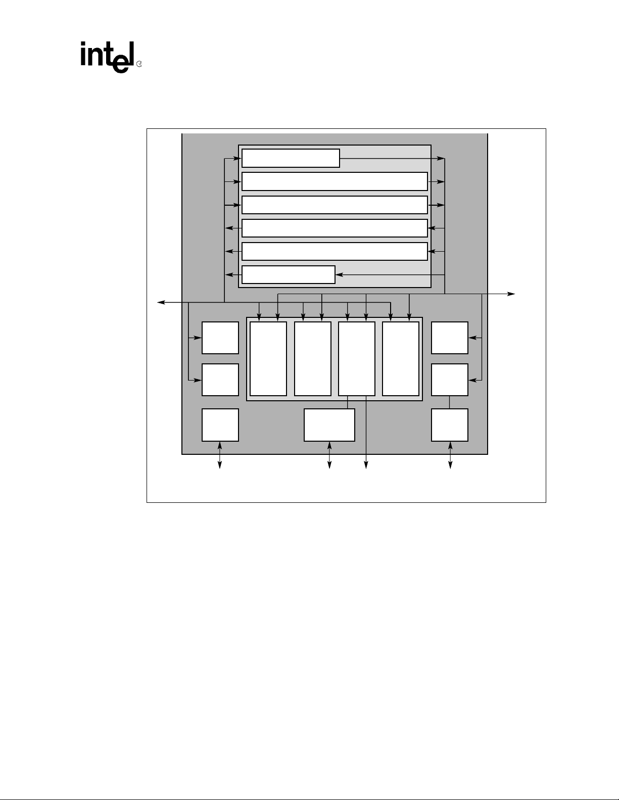
Figure 2 shows the 21555 microarchitecture.
Figure 2. 21555 Microarchitecture
21555
21555
Downstream Delayed Buffer
Downstream Posted Write Buffer
Upstream Read Data Buffer
Downstream Read Data Buffer
Upstream Posted Write Buffer
Introduction
rimary
PCI
Bus
Primary
Target
Control
Primary
Master
Control
JTAG
JTAG Signals
Upstream Delayed Buffer
Primary
Config
Registers
DeviceSpecific
Config
Registers
ROM Interface
ROM
Interface
Control
Signals
CSR
Registers
Interrupt
Signals
Secondary
Config
Registers
Secondary
PCI
Bus
Secondary
Target
Control
Secondary
Master
Control
Secondary
Bus
Arbiter
Secondary Arbiter
Signals
A7418-01
21555 Non-Transparent PCI-to-PCI Bridge User Manual 19
Page 20

Introduction
2.3 Special Applications
2.3.1 Primary Bus VGA Support
The 21555 provides hardware support that allows configuration of itself as a Video Graphics Adapter (VGA)
device. The primary class code should be preloaded through the serial ROM (SROM) or loaded by the local
processor with the value for a VGA device (Base Class 03h, Sub-Class 00h, Programming Interface 00h). This
allows the 21555 to present itself to the host as a VGA device.
The VGA Mode field in the Chip 0 Control register (see page 156) should be set to 01b to enable decoding of VGA
transactions on the primary bus for forwarding to the secondary bus. These bits can be set through SROM preload,
or either from a primary or secondary bus configuration write. Table 4 gives addresses that are decoded.
Table 4. Decoded and Not Decoded Addresses
Memory addresses [000BFFFFh : 000A0000h]
I/O addresses:
Bits not decoded.
AD[9:0]3BBh:3B0h
3DFh:3C0h
AD[31:16]000h
(No address translation is performed on these addresses.)
The 21555 cannot be enabled as a snooping agent on the primary bus. This is because the 21555 cannot guarantee
that it can buffer and forward all palette writes, since the 21555 has finite buffer space and no backoff mechanism
when snooping. The 21555 should not be configured to appear as a VGA device in those applications where it may
try to configure the 21555 as a snooping agent.
The parallel ROM can be used to store VGA BIOS code, which is mapped through the Primary Expansion ROM
BAR.
2.3.2 Secondary Bus VGA Support
The 21555 can be enabled to decode VGA transactions on the secondary bus for forwarding to the primary bus.
This is done by setting the VGA Enable field in the Chip Control 0 register to 10b. The addres ses that are decoded
are the same as for the primary VGA decode, and again the addresses are not translated.
Upstream forwarding of VGA transactions can be useful for applications that want to allow access to a primary bus
VGA device frame buffer by local processors in intelligent I/O or embedded subsystems.
Note: VGA decoding must not be enabled for both the pr imary and secondary interface. The value 11b is
illegal for the VGA Enable field and can yield unpredictable results.
2.4 Programming Notes
2.4.1 Addressing
The non-transparent addressing model that the 21555 uses can cause problems if not programmed properly.
Programming errors include:
20 21555 Non-Transparent PCI-to-PCI Bridge Use r Manual
Page 21

Introduction
• Setting a translated base address for a downstream range to fall within an address range defined for upstream
forwarding. This would cause the 21555 to respond as a target on the secondary bus to a downstream
transaction that it has initiated as a master. The transaction would then be forwarded back to the primary bus.
The address on the primary bus depends on the translated base address value for that upstream range.
• Setting a translated base address for an upstream range to fall within an add ress r a nge for down stream
forwarding. This results i n similar behavior described in the previous condition, but in the opposite direction.
• Enabling I/O subtractive decoding in both directions. When an I/O transaction is subtractively decoded on the
primary bus and forwarded downst r eam by t he 2 155 5, and no t arget responds on the secondary bus, the 21555
subtractively decodes the transaction on the secondary bus and forwards it back upstream. Since there is no
address translation for subtractively decoded I/O trans actions, this results in the 21555 forwarding the
transaction downstream and upstream forever.
• Enabling VGA decoding in both directions. Refer to subtractive I/O decoding in the previous bullet. Again,
there is the case of a non translated I/O address decoded by the 21555 on both interfaces as a target and
forwarded to the opposite interface.
2.4.2 Transaction Forwarding
When using the indirect I/O transaction generation mechanism, the low tw o bits of the I/O address in the I/O
Address register must match the byte enables as described in the PCI Local Bus Specification, Revision 2.2. The
21555 does not correct any discrepancies between the byte enables and address bits [1:0].
2.4.3 ROM Access
Parallel and SROM access mechanisms do not accommodate multiple masters. That is, when more than one master
attempts to access the ROM during the same time period, wrong data may be returned or written to the ROM. There
is no semaphore method to guarantee atomicity of the ROM address, data, and control register accesses.
This also applies to a parallel ROM access through the Primary Expansion ROM BAR at the same time a secondary
bus master might be accessing ROM registers.
21555 Non-Transparent PCI-to-PCI Bridge User Manual 21
Page 22

Page 23

Signal Descriptions 3
This chapter presents the theory of operation info rmation about the PCI sign al interface. See Chapter 16 for specific
information about PCI registers. Table 5 describes the PCI signal groups, function, and provides a page reference.
Table 5. Signal Pin Functional Groups
Group by Signal Pin Description See Page
All PCI pins required by the PCI Local
Primary Bus and
Extension interface
Signal Pins
Secondary Bus and
Extension Interface
Signal Pins
Miscellaneous Signal
Pins
Timing
Optional configuration
and expansion
memory.
Arbitration Primary PCI Bus Arbitration Signals Section 10.1 on page 97
Interrupt
Error Error Signals Section 12.1 on page 105
Test Access Port JTAG Signals Section 13.1 on page 111
Bus Specification, Revision 2.2.
All PCI 64-bit extension pins required
by the PCI Local Bus Specification,
Revision 2.2.
All PCI pins required by the PCI Local
Bus Specification, Revision 2.2.
All PCI 64-bit extension pins required
by the PCI Local Bus Specification,
Revision 2.2.
Two input voltage signaling pins. Section 3.5 on page 31
Power Management, Hot-Swap, and
Reset Signals
Primary and Secondary PCI Bus
Clock Signals
Interface Signals Section 8.1 on page 81
SROM Interface Signals Section 9.1 on page 91
Primary and Secondary PCI Bus
Interrupt Signals
Section 3.1 on page 24
Section 3.2 on page 26
Section 3.3 on page 28
Section 3.4 on page 30
Section 6.1 on page 65
Section 7.1 on page 77
Section 11.1 on page 101
21555 Non-Transparent PCI-to-PCI Bridge User Manual 23
Page 24

Signal Descriptions
3.1 Primary PCI Bus Interface Signals
Table 6 describes the primary PCI bus interface signals. The letters in the “Type” column are described in Table 1.
T able 6. Primary PCI Bus Interface Signals (Sheet 1 of 2)
Signal Name Type Description
Primary PCI interface address and data. These signals are a 32-bit multiplexed
address and data bus. During the address phase or phases of a transaction, the
p_ad[31:0] TS
p_cbe_l[3:0] TS
p_devsel_l STS
p_frame_l STS
p_idsel I
p_irdy_l STS
initiator drives a physical address on p_ad[31:0].
During the data phases of a transaction, the initiator drives write data, or the target
drives read data, on p_ad[31:0]. When the primary PCI bus is idle, the 21555 drives
p_ad to a valid logic level when p_gnt_l is asserted.
Primary PCI interface command and byte enables. These signals are a multiplexed
command field and byte enable field. During the address phase or phases of a
transaction, the initiator drives the transaction type on p_cbe_l[3:0].
When there are two address phases, the first address phase carries the
dual-address command and the second address phase carries the transaction type.
For both read and write transactions, the initiator drives byte enables on
p_cbe_l[3:0] during the data phases. When the primary PCI bus is idle, the 21555
drives p_cbe_l to a valid logic level when p_gnt_l is asserted.
Primary PCI interface DEVSEL#. Signal p_devsel_l is asserted by the target,
indicating that the device is responding to the transaction. As a target, the 21555
decodes the address of a transaction initiated on the primary bus to determine
whether to assert p_devsel_l.
As an initiator of a transaction on the primary bus, the 21555 looks for the assertion
of p_devsel_l within five clock cycles of p_frame_l assertion; otherwise, the 21555
terminates the transaction with a master abort.
Upon completion of a transaction, p_devsel_l is driven to a deasserted state for one
clock cycle and is then sustained by an external pull-up resistor.
Primary PCI interface FRAME#. Signal p_frame_l is driven by the initiator of a
transaction to indicate the beginning and duration of an access on the primary PCI
bus. Signal p_frame_l assertion (falling edge) indicates the beginning of a PCI
transaction. While p_frame_l remains asserted, data transfers can continue. The
deassertion of p_frame_l indicates the final data phase requested by the initiator.
Upon completion of a transaction, p_frame_l is driven to a deasserted state for one
clock cycle and is then sustained by an external pull-up resistor.
Primary PCI interface IDSEL. Signal p_idsel is used as the chip select line for Type
0 configuration accesses to 21555 configuration space from the primary bus. When
p_idsel is asserted during the address phase of a Ty pe 0 configuration transaction,
the 21555 responds to the transaction by asserting p_devsel_l.
Primary PCI interface IRDY#. Signal p_irdy_l is driven by the initiator of a
transaction to indicate the initiator’s ability to complete the current data phase on the
primary PCI bus.
During a write transaction, assertion of p_irdy_l indicates that valid write data is
being driven on the p_ad bus.
During a read transaction, assertion of p_irdy_l indicates that the initiator is able to
accept read data for the current data phase. Once asserted during a given data
phase, p_irdy_l is not deasserted until the data phase completes.
Upon completion of a transaction, p_irdy_l is driven to a deasserted state for one
clock cycle and is then sustained by an external pull-up resistor.
24 21555 Non-Transparent PCI-to-PCI Bridge Use r Manual
Page 25

T able 6. Primary PCI Bus Interface Signals (Sheet 2 of 2)
Signal Name Type Description
Primary PCI interface parity. Signal p_par carries the even parity of the 36 bits of
p_ad[31:0] and p_cbe_l[3:0] for both address and data phases. Signal p_par is
driven by the same agent that drives the address (for address parity) or the data (for
data parity). Signal p_par contains valid parity one clock cycle after the addres s is
valid (indicated by assertion of p_frame_l), or one clock cycle after the data is valid
p_par TS
p_req_l TS
p_stop_l STS
p_trdy_l STS
(indicated by assertion of p_irdy_l for write transactions and p_trdy_l for read
transactions). Signal p_par is tristated one clock cycle after the p_ad lines are
tristated.
The device receiving data samples p_par as an inpu t to check for possible parity
errors. When the primary PCI bus is idle, the 21555 drives p_par to a valid logic
level when p_gnt_l is asserted (one clock cycle after the p_ad bus is pa r ked).
Primary PCI bus REQ#. Signal p_req_l is asserted by the 21555 to indicate to the
primary bus arbiter that it wants to start a transaction on the primary bus. Signal
p_req_l is tristated during the assertion of chip reset.
Primary PCI interface STOP#. Signal p_stop_l is driven by the target of a
transaction, indicating that the target is requesting the initiator to stop the transaction
on the primary bus.
• When p_stop_l is asserted in conjunction with p_trdy_l and p_devsel_l
assertion, a disconnect with data transfer is being signaled.
• When p_stop_l and p_devsel_l are asserted, but p_trdy_l is deasserted, a
target disconnect without data transfer is being signaled. When this occurs on
the first data phase, that is, no data is transferred during the transaction, this is
referred to as a target retry.
• When p_stop_l is asserted and p_devsel_l is deasserted, the target is
signaling a target abort.
Upon completion of a transaction, p_stop_l is driven to a deasserted state for one
clock cycle and is then sustained by an external pull-up resistor.
Primary PCI interface TRDY#. Signal p_trdy_l is driven by the tar get of a
transaction to indicate the target's ability to complete the current data phase on the
primary PCI bus.
During a write transaction, assertion of p_trdy_l indicates that the target is able to
accept write data for the current data phase.
During a read transaction, assertion of p_trdy_l indicates that the target is driving
valid read data on the p_ad bus. Once asserted during a given data phase, p_trdy_l
is not deasserted until the data phase completes.
Upon completion of a transaction, p_trdy_l is driven to a deasserted state for one
clock cycle and is then sustained by an external pull-up resistor.
Signal Descriptions
21555 Non-Transparent PCI-to-PCI Bridge User Manual 25
Page 26

Signal Descriptions
3.2 Primary PCI Bus Interface 64-Bit Extension Signals
Table 7 describes the primary PCI bus interface 64-bit extension signals. The letters in the “Type” column are
described in Table 1.
T able 7. Primary PCI Bus Interface 64
Signal Name Type Description
Primary PCI interface acknowledge 64-bit transfer.
Signal p_ack64_l should never be driven when p_req64_l is not driven.
p_ack64_l STS
p_ad[63:32] TS
p_cbe_l[7:4] TS
Signal p_ack64_l is asserted by the target only when p_req64_l is asserted by the
initiator, to indicate the target’s ability to transfer data using 64 bits.
Signal p_ack64_l has the same timing as p_devsel_l.
When deasserting, p_ack64_l is driven to a deasserted state for one clock cycle
and is then sustained by an external pull-up resistor.
Primary PCI interface address and data upper 32 bits.
The 21555 does not bus park these pins. These pins are tristated during the
assertion of p_rst_l. Signals p _ad[63:32] are driven to a valid value when the 64-bit
extension is disabled (p_req64_l is deasserted during p_rst_l assertion).
This multiplexed address and data bus provides an additional 32 bits to the primary
interface. During the address phase or phases of a transaction, when the
dual-address command is used and p_req64_l is asserted, the initiator drives the
upper 32 bits of a 64-bit address; otherwise, these bits are unde fined, and the
initiator drives a valid logic level onto the pins.
During the data phases of a transaction, the initiator drives the upper 32 bits of
64-bit write data, or the target drives the upper 32 bits of 64-bit read data, when
p_req64_l and p_ack64_l are both asserted.
When not driven, signals p_ad[63:32] are pulled up to a valid logic level through
external resistors.
Primary PCI interface command and byte enables upper 4 bits.
The 21555 does not bus park these pins. These pins are tristated during the
assertion of p_rst_l. Signals p_cbe_l[7:4] are driven to a valid value when the
64-bit extension is disabled (p_req64_l is deasserted during p_rst_l assertion).
These signals are a multiplexed command field and byte enable field. During the
address phase or phases of a transaction, when the dual-address command is used
and p_req64_l is asserted, the initiator drives the transaction type on p_cbe_l[7:4];
otherwise, these bits are undefined, and the initiator drives a valid logic level onto
the pins.
For both read and write transactions, the initiator drives byte enables for the
p_ad[63:32] data bits on p_cbe_l[7:4] during the data phases, when p_req64_l
and p_ack64_l are both asserted.
When not driven, signals p_cbe_l[7:4] are pulled up to a valid logic level through
external resistors.
-Bit Extension Signals (Sheet 1 of 2)
26 21555 Non-Transparent PCI-to-PCI Bridge Use r Manual
Page 27

T able 7. Primary PCI Bus Interface 64-Bit Extension Signals (Sheet 2 of 2)
Signal Name Type Descrip tion
Primary PCI interface upper 32 bits parity.
The 21555 does not bus park this pin. This pin is tristated during the assertion of
p_rst_l. Signal p_par64 is driven to a valid value when the 64-bit extension is
disabled (p_req64_l is deasserted during p_rst_l assertion).
Signal p_par64 carries the even parity of the 36 bits of p_ad[63:32] and
p_cbe_l[7:4] for both address and data phases. Signal p_par64 is driven by the
initiator and is valid one clock cycle after the first address phase when a
dual-address command is used and p_req64_l is asserted. Signal p_par64 is also
p_par64 TS
p_req64_l STS
valid one clock cycle after the second address phase of a dual-address transaction
when p_req64_l is asserted. Signal p_par64 is valid one clock cycle after valid data
is driven (indicated by assertion of p_irdy_l for write data and p_trdy_l for read
data), when both p_req64_l and p_ack64_l are asserted for that data phase. Signal
p_par64 is tristated by the device driving read or write data one clock cycle after the
p_ad lines are tristated.
Devices receiving data sample p_par64 as an input to check for possible parity
errors during 64-bit transactions.
When not driven, p_par64 is pulled up to a valid logic level through external
resistors.
Primary PCI interface request 64-bit transfer.
Signal p_req64_l is sampled at secondary reset to enable the 64-bit extension on
the primary bus. When sampled low, the 64-bit extension is enabled.
Signal p_req64_l is asserted by the initiator to indicate that the initiator is requesting
64-bit data transfer. Signal p_req64_l has the same timing as p_frame_l. When
deasserting, p_req64_l is driven to a deasserted state for one clock cycle and is
then sustained by an external pull-up resistor.
The 21555 samples p_req64_l during primary bus reset to enable the 64-bit
extension signals. When p_req64_l is sampled high during reset, the primary 64-bit
extension is disabled and assumed not connected. The 21555 then drives
p_ad[63:32], p_cbe_l[7:4], and p_par64 to valid logic levels.
Signal Descriptions
21555 Non-Transparent PCI-to-PCI Bridge User Manual 27
Page 28

Signal Descriptions
3.3 Secondary PCI Bus Interface Signals
Table 8 describes the secondary PCI bus interface signals. The letters in the “Type” column are described in
Table 1.
Table 8. Secondary PCI Bus Interface Signals (Sheet 1 of 2)
Signal Name Type Description
Secondary PCI interface address and data. These signals are a 32-bit multiplexed
address and data bus. During the address phase or phases of a transaction, the
initiator drives a physical address on s_ad[31:0]. During the data phases of a
s_ad[31:0] TS
s_cbe_l[3:0] TS
s_devsel_l STS
s_frame_l STS
s_idsel I
s_irdy_l STS
transaction, the initiator drives write data, or the target drives read data, on
s_ad[31:0].
When the secondary PCI bus is idle, the 21555 drives s_ad to a valid logic level
when its secondary bus grant is asserted.
Secondary PCI interface command and byte enables. These signals are a
multiplexed command field and byte enable field. During the address phase or
phases of a transaction, the initiator drives the transaction type on s_cbe_l[3:0].
When there are two address phases, the first address phase carries the
dual-address command and the second address phase carries the transaction type.
For both read and write transactions, the initiator drives byte enables on
s_cbe_l[3:0] during the data phases.
When the secondary PCI bus is idle, the 21555 drives s_cbe_l to a valid logic level
when its secondary bus grant is asserted.
Secondary PCI interface DEVSEL#. Signal s_d evsel _l is asserted by the target,
indicating that the device is responding to the transaction. As a target, the 21555
decodes the address of a transaction initiated on the secondary bus to determine
whether to assert s_devsel_l. As an initiator of a transaction on the secondary bus,
the 21555 looks for the assertion of s_devsel _l within five clock cycles of
s_frame_l assertion; otherwise, the 21555 terminates the transaction with a master
abort.
Upon completion of a transaction, s_devsel_l is driven to a deasserted state for one
clock cycle and is then sustained by an external pull-up resistor.
Secondary PCI interface FRAME#. Signal s_frame_l is driven by the initiator of a
transaction to indicate the beginning and duration of an access on the secondary
PCI bus. Signal s_frame_l assertion (falling edge) indicates the beginning of a PCI
transaction. While s_frame_l remains asserted, data transfers can continue. The
deassertion of s_frame_l indicates the final data phase requested by the initiator.
Upon completion of a transaction, s_frame_l is driven to a deasserted state for one
clock cycle and is then sustained by an external pull-up resistor.
Secondary PCI interface IDSEL. Signal s_idsel is used as the chip select line for
Type 0 configuration accesses to 21555 configuration space from the secondary
bus. When s_idsel is asserted during the address phase of a Type 0 configuration
transaction, the 21555 responds to the transaction by asserting s_devsel_l.
Secondary PCI interface IRDY#. Signal s_irdy_l is driven by the initiator of a
transaction to indicate the initiator’s ability to complete the current data phase on the
secondary PCI bus.
During a write transaction, assertion of s_irdy_l indicates that valid write data is
being driven on the s_ad bus.
During a read transaction, assertion of s_irdy_l indicates that the initiator is able to
accept read data for the current data phase. Once asserted during a given data
phase, s_irdy_l is not deasserted until the data phase completes.
Upon completion of a transaction, s_irdy_l is driven to a deasserted state for one
clock cycle and is then sustained by an external pull-up resistor.
28 21555 Non-Transparent PCI-to-PCI Bridge Use r Manual
Page 29

Table 8. Secondary PCI Bus Interface Signals (Sheet 2 of 2)
Signal Name Type Descrip tion
Secondary PCI interface parity. Signal s_par carries the even parity of the 36 bits of
s_ad[31:0] and s_cbe_l[3:0] for both address and data phases. Signal s_par is
driven by the same agent that drives the address (for address parity) or the data (for
data parity). Signal s_par contains valid parity one clock cycle after the address is
valid (indicated by assertion of s_frame_l), or one clock cycle after the data is valid
s_par TS
s_stop_l STS
s_trdy_l STS
(indicated by assertion of s_irdy_l for write transactions and s_trdy_l for read
transactions). Signal s_par is tristated one clock cycle after the s_ad lines are
tristated. The device receiving data samples s_par as an input to check for possible
parity errors.
When the secondary PCI bus is idle, the 21555 drives s_par to a valid logic level
when its secondary bus grant is asserted (one clock cycle after the s_ad bus is
parked).
Secondary PCI interface STOP#. Signal s_stop_l is driven by the tar get of a
transaction, indicating that the target is requesting the initiator to stop the
transaction on the secondary bus.
When s_stop_l is asserted in conjunction with s_trdy_l and s_devsel_l assertion,
a disconnect with data transfer is being signaled.
When s_stop_l and s_devsel_l are asserted, but s_trdy_l is deasserted, a target
disconnect without data transfer is being signaled. When this occurs on the first data
phase, that is, no data is transferred during the transaction, this is referred to as a
target retry.
When s_stop_l is asserted and s_devsel_l is deasserted, the target is signaling a
target abort.
Upon completion of a transaction, s_stop_l is driven to a deasserted state for one
clock cycle and is then sustained by an external pull-up resistor.
Secondary PCI interface TRDY#. Signal s_trdy_l is driven by the target of a
transaction to indicate the target’s ability to complete the current data phase on the
secondary PCI bus.
During a write transaction, assertion of s_trdy_l indicates that the target is able to
accept write data for the current data phase.
During a read transaction, assertion of s_trdy_l indicates that the target is driving
valid read data on the s_ad bus. Once asserted during a given data phase, s_trdy_l
is not deasserted until the data phase completes.
Upon completion of a transaction, s_trdy_l is driven to a deasserted state for one
clock cycle and is then sustained by an external pull-up resistor.
Signal Descriptions
21555 Non-Transparent PCI-to-PCI Bridge User Manual 29
Page 30

Signal Descriptions
3.4 Secondary PCI Bus Interface 64-Bit Extension
Signals
Table 9 describes the secondary PCI bus interface 64-bit extension signals. The letters in the “Type” column are
described in Table 1.
T able 9. Secondary PCI Bus Interface 64
Signal Name Type Description
Secondary PCI interface acknowledge 64-bit transfer.
Signal s_ack64_l should never be driven when s_req64_l is not driven.
s_ack64_l STS
s_ad[63:32] TS
s_cbe_l[7:4] TS
Signal s_ack64_l is asserted by the target only when s_req64_l is asserted by the
initiator, to indicate the target’s ability to transfer data using 64 bits.
Signal s_ack64_l has the same timing as s_devsel_l. When deasserting,
s_ack64_l is driven to a deasserted state for one clock cycle and is then sustained
by an external pull-up resistor.
Secondary PCI interface address and data upper 32 bits.
The 21555 does not bus park these pins. These pins are tristated during the
assertion of s_rst_l. Signals s_ad[63:32] are driven to a valid value when the 64-bit
extension is disabled (s_req64_l is deasserted during s_rst_l assertion).
This multiplexed address and data bus provides an additional 32 bits to the
secondary interface. During the address phase or phases of a transaction, when the
dual-address command is used and s_req64_l is asserted, the initiator drives the
upper 32 bits of a 64-bit address; otherwise, these bits are unde fined, and the
initiator drives a valid logic level onto the pins. During the data phases of a
transaction, the initiator drives the upper 32 bits of 64-bit write data, or the target
drives the upper 32 bits of 64-bit read data, when s_req64_l and s_ack64_l are
both asserted.
When not driven, signals s_ad[63:32] are pulled up to a valid logic level through
external resistors.
Secondary PCI interface command and byte enables upper 4 bits.
The 21555 does not bus park these pins. These pins are tristated during the
assertion of s_rst_l. Signals s_cbe_l[7:4] are driven to a valid value when the
64-bit extension is disabled (s_req64_l is deasserted during s_rst_l assertion).
These signals are a multiplexed command field and byte enable field. During the
address phase or phases of a transaction, when the dual-address command is used
and s_req64_l is asserted, the initiator drives the transaction type on s_cbe_l[7:4];
otherwise, these bits are undefined, and the initiator drives a valid logic level onto
the pins. For both read and write transactions, the initiator drives byte enables for
the s_ad[63:32] data bits on s_cbe_l[7:4] during the data phases, when s_req64_l
and s_ack64_l are both asserted.
When not driven, signals s_cbe_l[7:4] are pulled up to a valid logic level through
external resistors.
-Bit Extension Signals (Sheet 1 of 2)
30 21555 Non-Transparent PCI-to-PCI Bridge Use r Manual
Page 31

Signal Descriptions
Table 9. Secondary PCI Bus Interface 64-Bit Extension Signals (Sheet 2 of 2)
Signal Name Type Descrip tion
Secondary PCI interface upper 32 bits parity.
The 21555 does not bus park this pin. This pin is tristated during the assertion of
s_rst_l. Signal s_par64 is driven to a valid value when the 64-bit extension is
disabled (s_req64_l is deasserted during s_rst_l assertion).
Signal s_par64 carries the even parity of the 36 bits of s_ad[63:32] and
s_cbe_l[7:4] for both address and data phases. Signal s_par64 is driven by the
initiator and is valid one clock cycle after the first address phase when a
dual-address command is used and s_req64_l is asserted. Signal s_ par64 is also
s_par64 TS
s_req64_l STS
valid one clock cycle after the second address phase of a dual-address transaction
when s_req64_l is asserted. Signal s_par64 is valid one clock cycle after valid data
is driven (indicated by assertion of s_irdy_l for write data and s_trd y_l for read
data), when both s_req64_l and s_ack64_l are asserted for that data phase. Signal
s_par64 is tristated by the device driving read or write data one clock cycle after the
s_ad lines are tristated.
Devices receiving data sample s_par64 as an input to check for possible parity
errors during 64-bit transactions.
When not driven, s_par64 is pulled up to a valid logic level through external
resistors.
Secondary PCI interface request 64-bit transfer.
Signal s_req64_l is sampled at secondary reset to enable the 64-bit extension on
the secondary bus. When sampled low, the 64-bit extension is enabled. W hen
designated as a secondary bus central function, the 21555 asserts this signal during
secondary bus reset.
Signal s_req64_l is asserted by the initiator to indicate that the initiator is requesting
64-bit data transfer. Signal s_req64_l has the same timing as s_frame_l. When the
21555 is the secondary bus central function, it will assert s_req64_l low during
secondary bus reset to indicate that a 64-bit bus is supported. When deasserting,
s_req64_l is driven to a deasserted state for one clock cycle and is then sustained
by an external pull-up resistor. The 21555 samples s_req64_l during secondary bus
reset to enable the 64-bit extension signals. When s_req64_l is sampled high
during reset, the secondary 64-bit extension is disabled and assumed not
connected. The 21555 then drives s_ad[63:32], s_cbe_l[7:4], and s_par64 to valid
logic levels.
3.5 Miscellaneous Signals
Table 10 describes th e mi scellaneous signals. The letters in the “Type” column are described in Table 1.
Table 10. Miscellaneous Signals
Signal Name Type Description
Primary interface I/O voltage. This signal must be tied to either 3.3 V or 5.0 V,
p_vio I
s_vio I
21555 Non-Transparent PCI-to-PCI Bridge User Manual 31
corresponding to the signaling environment of the primary PCI bus as described in
the PCI Local Bus Specification, Revision 2.2. When any device on the primary PCI
bus uses 5-V signaling levels, tie p_vio to 5.0 V. Signal p_vio is tied to 3.3 V only
when all the devices on the primary bus use 3.3-V signaling levels.
Secondary interface I/O voltage. This signal must be tied to either 3.3 V or 5.0 V,
corresponding to the signaling environment of the secondary PCI bus as described
in the PCI Local Bus Specification, Revision 2.2. When any device on the
secondary PCI bus uses 5-V signaling levels, tie s_vio to 5.0 V. Signal s_vio is tied
to 3.3 V only when all the devices on the secondary bus use 3.3-V signaling levels.
Page 32

Page 33

Address Decoding 4
This chapter presents the theory of operation information abo ut add res s mapping and deco ding. See Chapter 16 for
specific information about addressing registers. The following areas are covered:
• Section 4.1, “CSR Address Decoding” on page 34.
• Section 4.2, “Expansion ROM Addre s s Mapping (Decoding)” on page 34.
• Section 4.3, “Memory 0 Transaction Address Decoding” on page 34 .
• Section 4.4, “I/O Transaction Address Decoding” on page42.
• Section 4.5, “Configuration Accesses” on page 44.
The 21555 implements separate Base Address Regis ters (BARs) on both the pr imary and s econdary interfaces. The
BARs denotes address ranges for downstream and upstream forwarding. This addressing is unlike the transparent
PCI-to-PCI Bridge (PPB), discussed in Chapter 2, which implements a flat address map encompassing both the
primary and secondary interfaces.
The 21555 BARs denote interface ranges for Co ntrol and Status Registers (CSR) access.
• Primary Interface – The 21555 responds t o those transact ions whose addr esses fall into one of its pri mary BAR
ranges. All other I/O and memory transactions on the primary bus are ignored by the 21555. The address
ranges defined by the primary BARs reside in the primary, or system, address map.
• Secondary Interface – The 21555 responds to those transactions whose addresses reside in one of the
secondary BAR ranges. All other transactions on the secondary bus are ignored by the 21555. The address
ranges defined by the secondary BARs reside in the secondary, or local, address map.
The system and local address maps are independent of each other . The 21555 supports addres s translations between
the two address maps when forw arding transactions upstream or downstream.
Note: When enabled as a target, the 21555 ignores any transactions that it initiates as a master with the
exception of type 0 configuration transactions.
21555 Non-Transparent PCI-to-PCI Bridge User Manual 33
Page 34

Address Decoding
4.1 CSR Address Decoding
The 21555 implements a set of CSRs that are mapped in memory or in I/O space. The registers are mapped
independently on the primary and secondary interfaces. The following BARs are used for CSR mapping:
• The primary CSR and:
— Downstream Memory 0 BAR is for mapping in primary bus memory address space. The Lower 4KB of
this range used to map the 21555 CSRs.
— I/O BAR is for mapping i n primary bus I/O space.
• The secondary CSR:
— Memory BAR is for mapping in secondary bus memory address space.
— I/O BAR is for mapping i n secondary bus I/O space.
The primary BARs are located in the 21555 primary bus configuration space, and the secondary BARs are located
in the 21555 secondary bus configuration space. The memory BARs reques t 4 KB each (minimum size for Primary
CSR and Downstream Memory 0 BAR), and t he I/O BARs request 256 bytes each.
4.2 Expansion ROM Address Mapping (Decoding)
The 21555 implements one BAR, the Primary Expansion Read Only Memory (ROM) BAR, to map the expansion
ROM that can be attached to the 21555. The Expansion ROM can be mapped into primary bus address space only,
and is not accessible through a BAR from the secondary bus. The size of the Primary Expansion ROM BAR is
programmable through the Primary Expansion ROM Setup register in device-s pecific configuration space. The size
may vary from 4 KB to 16 MB by powers of 2. The Primary Expansion ROM BAR can also be disabled through
theSetup register so that it does not request space when the expansion ROM is not implemented.
4.3 Memory 0 Transaction Address Decoding
The BARs can be enabled to decode and forward memory transactions to the opposite interface. The 21555
implements primary interface and secondary interface BARs:
• The downstream BARs are in primary configuration space. The BARs decode transactions on the primary bus
to be forwarded to the secondary bus.
— Primary CSR and Downstream Memory 0.
— For addresses above the low 4 KB in this address range.
— Upstream I/O or Memory 0.
— Upstream Memory 1.
— Upstream Memory 2.
• The upstream BARs are in secondary confi guration space. The BARs decode transactions on the secondary
bus to be forwarded to th e primary bus.
— Downstream I/O or Memory 1.
— Downstream Memory 2.
— Downstream Memory 3.
34 21555 Non-Transparent PCI-to-PCI Bridge Use r Manual
Page 35

Address Decoding
4.3.1 Using the BAR Setup Registers
All downstream and upstream BARs have programmable sizes, and can be disabled so that they request no space.
The Primary CSR and Downstream Memory 0 BAR canno t be totally disabled, as the 21555 CSRs are always
mapped in the bottom 4KB. The forwarding part of the range can be disabled by requesting only 4KB of memory
Table 12 on page 47 summarizes the minimum and maximum range for each address range). In addition, the
Downstream Memory 3 BAR can be configured to be mapped in 64-bit address space. The register then compris es
two 32-bit registers and can be used for forwarding DACs downstream. 64-bit addressing support is discussed
further in Section 4.3.5 on page 41. These BARs can also be programmed to be prefetchable or non-prefetchable.
Programming of all the forwarding BARs with the exception of the Upstream Memory 2 BAR is done through
corresponding device-specific Setup configuration registers. The Primary Expansion ROM BAR also has a Setup
register. Setup registers are preloaded by the serial ROM and can also be written from the secondary interface. Each
bit of the Setup register corresponds to the same bit of its respective BAR.
Bit 0 of the Downstream I/O or Memory 1 Setup register and Upstream I/O or Memory 0 Setup register (see
Section 16 on page 121) should be written with:
• A zero (0) to select a memory BAR.
• A one (1) to select an I/O BAR. Bits [2:1] are writable to select the type of memory mapping. The Downstream
Memory 3 Setup registers bits [2:1] may be set to 10b to select 64-bit addressing.
A mask is used to set the size of the BAR for the remaining read/write bits of the Setup register. Writing a 1 sets the
corresponding bit in that Setup register’s BAR to be read/write. Writing a 0 (zero) sets the corresponding bit in that
Setup register’s BAR to be read only as 0. Therefore, the size is set by writing the appropriate number of most
significant bits to a 1, and the remaining bits to a 0. When all of the zeros and ones in the size field are not
contiguous, this is illegal and unpredictable results may occur. When the most significant writable bit of the Setup
register is a 0, the corresponding BAR is disabled and requests no space.
Figure 3 shows an example of using a Setup regis ter to program a BAR to request 1 MB of memory space.
Figure 3. BAR Setup Register Example
31 20 19
111111111111
31 0
bbbbbb
R/W (Base Address)
bbbbbb
Setup Register
0000000000000001001
20 19
000000000000000010001
Read Only
Base Address Register
0
A7461-01
21555 Non-Transparent PCI-to-PCI Bridge User Manual 35
Page 36

Address Decoding
4.3.2 Direct Address Translation
With the exception of secondary bus transactions falling into the Upstream Memory 2 address
range (see Section 4.3.3) and all dual address transactions (Section 4.3.5), the 21555 uses direct address translation
when forwarding memory transactions from one interface to the other. Note that since transactions addressing the
bottom 4 KB of the Primary CSR and Downstream Memory 0 BAR are targeted at the 21555 CSRs, no forwarding
and therefore no address translation is performed. Direct address translation is used for transactions in that range
above the low 4 KB boundary.
A memory address may be thought of as a base address (as programmed in the Downstream and Upstream BARs)
with an offset from the base address, as shown in Figure 4.
Figure 4. Address Format
Address Map
Address
Offset
Base Address
Base Offset
A7462-01
When a memory transaction is forwarded downstream from the primary bus to the secondary bus, the primar y bus
address can be mapped to another address in the secondary bus domain. The mapping is performed by substituting
a new base address for the base of the original address, as shown in Figure 5.
36 21555 Non-Transparent PCI-to-PCI Bridge Use r Manual
Page 37

Address Decoding
This new base address, also called the translated base address, references a new location in the
secondary bus address map. The offset is not affected. The process is similar for transactions
forwarded from the secondary bus to the primary bus.
Figure 5. Direct Offset Address Translation
Base
Translated Base
Offset
Offset
Original Address
Translated Address
A7463-01
Each memory address range using direct offset address translation has its own translated base. The translated base
addresses are programmable in registers corresponding to each BAR. These registers are mapped both in
device-specific configuration space and in CSR space. The number of bits of the translated base address
corresponds to the number of writable bits in the respective BAR. Likewise, the number of bits of t he offset also
varies and depends on the size of the BAR. Figure 6 shows an example of address translation of downstream
memory transactions. Again, upstream transactions are treated similarly.
Figure 6. Downstream Address Translation Example
Primary Address Map Secondary Address Map
Base + Offset
Translated
Base + Offset
A7464-01
4.3.3 Lookup Table Based Address Translation
As mentioned in Section 4.3.2, Upstream Memory 2 addr ess translation is treated dif f erently than the other ranges.
The 21555 uses a page size based lookup table to perform address translation for transactions falling into this range.
A lookup table provides a flexible way of translating secondary bus local addresses to primary bus system
addresses.
21555 Non-Transparent PCI-to-PCI Bridge User Manual 37
Page 38

Address Decoding
The Upstream Memory 2 address range consists of a fixed number (64) of pages. The page size is
programmable in the Chip Control 1 configuration register. Therefore, the size of the Upstream
Memory 2 BAR is dependent on the page size. The page size varies between 256 bytes to 32 MB
by powers of 2. This results in a window size that varies from 16 KB to 2 GB. This BAR can also
be disabled.
Each page of the upstream window has a corresponding translated base address.
The size of the translated base address varies with the page size and window size. The translated base address
replaces both the original base address and the lookup table index bits. The address bits used for the original base
address for a given page and window size are listed in Table 11, as well as the locations of the six address bits
needed to select one of the 64 entries in th e loo kup table. The offset of the address, which is not translated, consists
of the remaining lower order address bits. Table 11 shows the Upstream Memory 2 window size, with base address,
index, and offset fields.
Table 11. Upstream Memory 2 Window Size
Page Size
(bytes)
256 16K [31:14] [13:8] [7:0]
512 32K [31:15] [14:9] [8:0]
1K 64K [31:16] [15:10] [9:0]
2K 128K [31:17] [16:11] [10:0]
4K 256K [31:18] [17:12] [11:0]
8K 512K [31:19] [18:13] [12:0]
16K 1M [31:20] [19:14] [13:0]
32K 2M [31:21] [20:15] [14:0]
64K 4M [31:22] [21:16] [15:0]
128K 8M [31:23] [22:17] [16:0]
256K 16M [31:24] [23:18] [17:0]
512K 32M [31:25] [24:19] [18:0]
1M 64M [31:26] [25:20] [19:0]
2M 128M [31:27] [26:21] [20:0]
4M 256M [31:28] [27:22] [21:0]
8M 512M [31:29] [28:23] [22:0]
16M 1G [31:30] [29:24] [23:0]
32 2G [31] [30:25] [24:0]
Window Size
(bytes)
Base Address
(bits)
Lookup Table Index
(bits)
Offset
(bits)
38 21555 Non-Transparent PCI-to-PCI Bridge Use r Manual
Page 39

Address Decoding
Figure 7 shows how a translated address is built using the lookup table, assuming a page size of 4 KB.
Figure 7. Address Translation Using A Lookup Table
Translated Base Look-up Table
3F
3E
3D
3C
3B
3A
39
Translated Base Address [3F]
Translated Base Address [3E]
Translated Base Address [Index]
7
6
5
4
3
2
1
0
Translated Base Address [1]
Translated Base Address [0]
31 18 17 0
Base Index Offset
31 0
Translated Base
12 11
12 11
Offset
A7465-01
Figure 8 shows an example of how different address regions might be forwarded upstream using the lookup table
address translation.
The lookup table is implemented on-chip and no external memory is needed. The lookup table is part of the
memory space that the 21555 requests with its Primary CSR Memory BAR and Secondary CSR Memory BAR.
The lookup table is also indirectly accessible in I/O or memory space at offsets 24h and 28h.
21555 Non-Transparent PCI-to-PCI Bridge User Manual 39
Page 40

Address Decoding
Note: The indirect access mechanism must be used only by one interface at a time. When access to the
lookup table by multiple masters is possible, it is strongly recommended that the Generic Own bits
or some other semaphore mechanism be used to restrict access to one master at a time.
Figure 8. Upstream Lookup Table Address Translation
Primary Address Map Secondary Address Map
Translated
Base + Offset
Base + Offset
A7466-01
The 21555 conditionally asserts s_inta_l when an upstream memory transaction transfers data addressing the last
Dword in a page. This interrupt alerts the local proces sor that the page entry may need updating. The 21555
implements an event bit and interrupt mask bit for each of the 64 pages (entries) in the upstream window.
Note: The page entry of the lookup table should not be updated while th e initiator is still performing
transactions addressing that page.
4.3.4 Lookup Ta ble Entry Format
Figure 9 shows the format for an entry in the lookup table. The number of bits of the entry used for the new
translated base address is variable and is listed in Table 11. The maximum number of bits used are bits [31:8],
corresponding to a 256-byt e page size, while the minimum number of bits used is bit [31], corresponding to a 32
Mbyte page size. The next 4 to 27 bits, depending on the number of bits used for the base address, are reserved. The
low 4 bits are used for control. Two control bits are defined, one indicating whether the entry is a valid entry, and
one indicating whether prefetchable behavior should be used on memory reads. When the entry is not valid, the
21555 treats the transaction addressing that page as if a master abort were detected on the target interface.
For writes, the 21555 discards memo ry wr ite data an d asser ts s_serr_l, when the SERR# Disable for Master Abort
during Posted Write bit is 0. For reads, the 215 55 ret urns FFFFFF FFh on reads if the Master Abort Mode bit is 0, or
returns a target abort if the Master Abort Mode bit is a 1.
40 21555 Non-Transparent PCI-to-PCI Bridge Use r Manual
Page 41

Address Decoding
Note: The lookup table is not cleared by reset. The lookup table must be initialized by the local processor
before the Upstream Memory 2 Address range is used.
Figure 9. Lookup Table Entry Format
31 18 17 8 7 3 2410
Translated Base Address
Translated Base Address
or Reserved
Prefetchable
Reserved
Reserved
Reserved
Valid
A7467-01
4.3.5 Forwarding of 64-Bit Address Memory Transactions
The 21555 considers the host and local memory space above the 4 GB boundary to be shared. This means that the
21555 uses a flat address map in this space. Dual-address cycle (DAC) transactions are used for addressing above
the 4 GB boundary. The 21555 can forward dual-address cycle transactions both upstream and downstream. The
Downstream Memory 3 BAR is used to designate the address range for downstream DACs. Inverse decoding is
used for upstream DACs.
The Downstream Memory 3 BAR may be configured to be a 64-bit BAR by preloading the Downstream Memory 3
Upper 32 Bits Setup reg ister b i t [31 ] to a one. The Downstream Memory 3 Setup register bits [2:1 ] s ho uld b e s et to
10b. This implies that the memory range can be located anywhere in 64-bit address space. When this 64-bit
addressing option is used, the maximum window size changes from 2 GB (in the 32-bit case) to 2
63
bytes.
When the preloaded window size for a 64-bit BAR is 2 GB or less, the space requested may be mapped either in
32-bit address space or 64-bit address space. In the former case, the upper 32 bits of the base address is zero and
transactions are forwarded as described in the previous section using direct offset address translation. When the
upper 32-bit base address is non-zero, the memory range is located above the 4 GB boundary.
When the Downstream Memory 3 Range is mapped above the 4 GB boundary , primary bus transactions falling into
this address range are forwarded downstream with no address translation performed. Any 64-bit address
transactions on the secondary bus falling outside of the Downstream Memory 3 address range are forwarded
upstream, again with no address translation. This is similar to the forwarding mechanisms of a transparent PPB
(21154) and is illustrated in Figure 10.
Note: Since the use of BARs restricts the alignment of the address range to the window size, the
Downstream Memory 3 address range can never straddle the 4 GB boundary. The base addres s of
21555 Non-Transparent PCI-to-PCI Bridge User Manual 41
Page 42

Address Decoding
the Downstream memory 3 address range must be set to a non-zero value when the upper 32 bits
.
are enabled (a base address of 0 is not allowed).
Figure 10. Dual
-Address Transaction Forwarding
Base + Offset
64
Byte Boundary
2
4GB Boundary
Translated
Base + Offset
Primary Address Map Secondary Address Map
A7468-01
4.4 I/O Transaction Address Decoding
The 21555 provides a mechanism where one BAR on each interface can be configured to be an I/O BAR instead of
a memory BAR. The Downstream I/O or Memory 1 BAR in pr imary conf iguration s pace is used to decode primary
bus I/O transactions for forwarding to the secondary bus. The Upstream I/O or Memory 0 BAR in secondary
configuration space is used to decode secondary bus I/O transactions for forwarding to the primary bus. (See
Table 37 on page 133.)
The 21555 performs direct offset address translation when forwarding I/O transactions in much the same manner
that it translates memory addresses. The size of the I/O BARs can be configured to be 64 bytes, 128 bytes, or 256
bytes. Accordingly, the base address can consist of 26, 25, or 24 bits. The 21555 hardware does not restrict setting
up larger I/O windows, although requ est ing more than 256 bytes of I/O space is a violation of the PCI Local Bus
Specification, Revision 2.2. The upper bits comprising the base address of the I/O addr ess on the primary bus is
replaced with the base address written in the Downstream I/O or Memory 1 Translated BAR when initiated on the
secondary bus. Similarly, the Upstream I/O or Memory 0 Translated BAR is used for upstream I/O transactions.
These translated base registers are mapped in both device-specific configuration space and the 21555 CSR space.
4.4.1 Indirect I/O Transaction Generation
The 21555 implements a CSR mechanism that allows access to any I/O address in the secondary or local I/O
address map from the primary interface, or any I/O address in the primary or host I/O address map from the
secondary interface. A pair of device-specific CSR registers contain the address and data used to initiate the I/O
42 21555 Non-Transparent PCI-to-PCI Bridge Use r Manual
Page 43

Address Decoding
transaction. One pair is used for downstream I/O transactions and one pair is used for upstream I/O transactions.
The downstream registers can only be accessed from the primary interface, and the upstream registers can only be
accessed from the secondary interface. Their function is similar, so only the downstream case is discussed.
The Downstream I/O Address register contains the address used when the transaction is initiated on the secondary
bus. When the Downstream I/O Data register is read or written from the primary interface, the 21555 initiates the
transaction on the secondary bus. For writes, the Downstream I/O Data register contains the write data to be
written. For reads, the read data is placed in this register upon completion of the secondary bus I/O read.
The I/O Data register must be accessed with an I/O transaction on the primary interface to in itiate the secondary bus
I/O transaction. Otherwise, this register appears as reserved for both memory accesses or accesses from the
secondary interface. The Downstream I/O Control bit in the I/O CSR must be set to enable downstream I/O
transaction generation; otherwise, I/O Data register accesses are treated as reserv ed accesses.
The 21555 uses the same byte enables that the initiator used to read or write the register.
Note: The low bits of the I/O address in the I/O Address register must match t he byte enables as
described in the PCI Local Bus Specification, Revision 2.2. The 21555 will not correct
discrepancies between byte enables and address bits [1:0].
The 21555 responds to read or write access of Downstream I/O Data register with a target retry until the access is
completed on the secondary bus. This I/O access is treated as a delayed transaction by the 21555. This delayed
transaction is entered into the 21555’s downstream delayed transaction queue and is ordered with respect to all
other downstream transactions. When ordering rules permit, the 21555 initiates I/O write or read on the secondary
bus. When the I/O transaction completes, the 21555 returns target termination and, if a read, returns read data when
the initiator repeats the transaction.
The 21555 provides a semaphore method that may be used to guarantee atomicity of the Downstream I/O Address
and Downstream I/O Data register accesses using the Downstream I/O Own bit. Atomicity of these accesses is not
hardware-enforced. An Upstream I/O Own bit is provided for upstream I/O transactions. The following procedure
should be used for downstream
I/O transactions:
1. The initiator of the transaction reads the Downstream I/O Own bit. When the bit reads as zero, the initiator can
proceed with the indirect I/O transaction sequence. When t he bit reads as a 1, the initiator should not proceed
until a subsequent read of the own bit returns a 0 (zero). The 21555 automatically sets the own bit to a 1after it
is read from the primary interface.
2. The initiator writes the target I/O address in the Downstream I/O Address register.
3. The initiator should write or read the data in the Downstream I/O Data register until a response other than
target retry is received.
4. Upon returning the completion of the I/O transaction to the initiator, the 21555 automatically clears the bit to a
0.
The same procedure should be used for upstream I/O transactions using the Upstream I/O Address register,
Upstream I/O Data register, and Upstream I/O Own bit. To read the state of the Downstream and Upstream I/O
Own bits without side effects, a read-only copy of the I/O Own bit states is kept in the I/O CSR. Byte access of the
I/O Own bits and their
read-only copies should be used to avoid setting the I/O Own bit for the opposite interface.
21555 Non-Transparent PCI-to-PCI Bridge User Manual 43
Page 44

Address Decoding
4.4.2 Subtractive Decoding of I/O Transactions
The 21555 can be enabled to subtractively decode I/O transactions and forward these transactions to the opposite
bus. No address translation is performed on subtractively decode d I/O transactions. The transaction is treated by the
21555 as a delayed transaction.
Note: Even when a subtractively-decoded delayed transaction is queued, the 21555 continues to respond
to the transaction on the initiator bus with subtractive timing.
To enable subtractive decoding of I/O transactions on the primary bus, the Subtractive Decode Enable bits in the
Chip Control 1 configuration register must be set to 01b. To enable subtractive decoding of I/O transactions on the
secondary bus, the Subtractive Decode Enable bits must be set to 10b.
There can be only one subtractive decoding agent on a PCI bus. Subtractive decoding should not be enabled for
both the primary and secondary interfaces.
4.5 Configuration Accesses
The 21555 responds to Type 0 configuration transactions on both its primary and secondary interfaces. The 21555
has two sets of configuration registers, one for the primary interface and one for the secondary interface. Both sets
are accessible from either interface. The 21555 can act as an initiator of Type 0 or Type 1 configuration transactions
on the primary or secondary bus using the indirect configuration transaction mechanism.
4.5.1 Type 0 Accesses to 21555 Configuration Space
The 21555 responds as a target to Type 0 configuration transactions on both its primary and secondary interfaces
when the IDSEL pin for that interface is asserted. The 21555 is a single function device so it does not decode the
function number. The 21555 can respond to configuration transactions regardless of the state of the posted write
and delayed transaction queues. Because the 21555 is not a transparent PPB (211 54), it does not respond to Type 1
configuration transactions.
Access to the 21555 configuration space may be restricted during different phases of initialization:
• Reset:
No access to the 21555 configuration space from either interface.
• Serial preload:
No access to the 21555 configuration space from either interface. the 21555 returns target retry.
• Optional primary lockout:
Access to the 21555 configuration space is allowed from the secondary interface only, until the Primary
Lockout Bit in the Chip Control 0 register is cleared. The 21555 returns target retry to all accesses initiated on
the primary bus, with the exception of accesses to the Table 123, “Reset Co ntrol Register” on page 188 at
Dword D8h.
• Normal configuration and operation:
Access to the 21555 configuration space is allowed from both the primary and secondary interfaces.
See Chapter 2 for a more detailed description of the initialization process.
During normal configuration and operation, when th e 215 55 d ecod es a configu ration access on one interface while
an access to a configuration register is already ongoing on the other interface, the 21555 holds the second initiator
in wait states until the first transaction is complete, and then completes the second transaction.
44 21555 Non-Transparent PCI-to-PCI Bridge Use r Manual
Page 45

Address Decoding
Accesses to the 21555 configuration s pace are not o rdered with respect to tr ansactions in the 2155 5 queues. T hat is,
the 21555 responds immediately to configuration transactions regardless of what transactions exist in the upstream
and downstream queues. Exceptions to this are configuration accesses that result in the initiation of config uratio n
and I/O transactions by the 21555. Thes e transactions are entered in the delayed transaction queue and ordered
appropriately with respect to other delayed transactions and posted writes in the 21555 queues.
4.5.2 Initiation of Configuration Transactions by 21555
Usually, the host processor configures primary bus devices and the local processor configures secondary bus
devices, so forwarding of configuration transactions is not typically necessary. However, to support other
configuration methods, the 21555 implements a mechanism that enables initiatio n of Type 0 or Type 1
configuration accesses on either the primary bus or the secondary bus. This mechanism is different from the
hierarchical mechanisms supported by PPBs. Instead, two pairs o f device-s pecific r egis ters contain the address and
data that are used to initiate the configuration transaction. One pair is used to generate transactions on the primary
interface; the other is used to generate transactions on the s econdary interface:
• The Upstream Configuration Address and Upstream Configuration Data register s cont ain the addr ess and data
of the configuration transaction to be initiated on the primary bus.
• the Downstream Configuration Address and Downst ream Configur ation Data registers contain the add ress and
data of the configuration transaction to be initiated on the secondary bus.
In addition, the Configuration CSR and Configuration Own Bits register ar e us ed for config uratio n transaction
generation. All of these registers are mapped into both device specific configuration space and the 21555 CSR
space. The upstream address and data registers can be written from the secondary interface only, and the
downstream address and data registers can be written from the primary interface only. Downstream and upstream
configuration address registers can be read from either interface. Otherwise, these registers respond as reserved.
To generate a configuration transaction, the correspond ing Upstream or Downstream Configuration Control bit in
the Configuration CSR must be set. Otherwise, the corresponding Configuration Data registers are treated as
reserved registers. The Configuration Data registers are also treated as reserved registers in memory space.
The Upstream or Downstream Configuration Address register must be written with the address to be driven before
the corresponding data register is accessed. This address is driven on the AD lines exactly as written in the register.
Therefore, a Type 0 format must be used to generate a
Ty pe 0 con fi gurat ion t rans acti on, and a Type 1 format must be used to generate a Type 1 configuration transaction.
The upper 21 bits of a Type 0 address format are used as IDSEL signals and are specific to the motherboard or
add-in card application.
The configuration transaction is initiated by the 21555 when the Upstream or Downstream Configuration Data
register is either read or written from the secondary or primary interface, respectively. These registers must be
accessed by either a configuration transaction or an I/O transaction to initiate the transaction. The 21555 uses the
same byte enables that the initiator used to read or write the register. The 21555 responds to the access of the
Upstream or Downstream Configuration Data register with a target retry until the access is completed on the target
bus. When the access is completed, the 21555 returns the corresponding target termination and, if a read, the read
data on a subsequent attempt of the transaction by the initiator . Wh en the Delayed T ransaction Target Retry Counter
expires, that is, 2
Delayed Transact ion Target Retry Counter may be dis abled, and thus does not limit the number of retries , by setti ng
the Retry Counter Disabl e bit in the Chip Control 0 configuration register.
The 21555 can be enabled to respond to configuration transactions that it generates by setting the appropriate
Downstream/Upstream Self-Response Enable bit in the Configuration CSR. For the 21555 to respond, the
transaction must assert the 21555’s IDSEL signal on that interface, and it must be a Type 0 configuration
transaction. When this bit is not set, the 21555 will not respond to any configuration transactions that it generates,
and these transactions may end in master abort.
24
target retries are received from the target, the 21555 returns a target abort to the initiator. The
21555 Non-Transparent PCI-to-PCI Bridge User Manual 45
Page 46

Address Decoding
The 21555 provides a semaphore method that may be used to guarantee atomicity of the address and data register
accesses using the Upstream Configuration Own bit and Downstream Configuration Own bit. Atomicity of these
accesses is not guaranteed in hardware. When the corresponding Configuration Enable b it is not set, the Own bit is
treated as reserved. The following procedure should be used for downstream transactions:
1. The initiator of the transaction should read the Downstream Configuration Own bit for initiation of
transactions on the secondary bus. When the bit reads as zero, the initiator may proceed with the configuration
transaction sequence. When the bit reads as a one, the initiator should not proceed until a subsequent read of
the own bit returns a 0 (zero). The 21555 automatically sets the own bit to a 1 after it is read.
2. The initiator should write the target configuration address in the Downstream Configuration Address r egister.
3. The initiator should write or read the data in the Downstream Configuration Data register until a response other
than target retry is received.
4. Upon completion of the configuration transaction on the initiator bus, the 21555 automa tically clears the
Downstream Configuration Own bit to a 0.
Upstream configuration transactions should us e a similar process. To check the status of the own bits without read
side effects, read only copies of these bits are located in the Configuration CSR. Byte access of the Configuration
Own bits and their read-only copies should be used to avoid setting the Configuration Own bi t for the oppo site
interface.
46 21555 Non-Transparent PCI-to-PCI Bridge Use r Manual
Page 47

4.6 21555 Bar Summary
Table 12 shows a summary of the 21555 BARs.
T a ble 12. Bar Summary
Bar Size Address Translation
Primary CSR and Downstream
Memory 0
Primary CSR I/O 256 byt es —
Secondary CSR Memory 4 KB —
Secondary CSR I/O 256 bytes —
Primary Expansion ROM 4 KB to 16 MB —
Downstream I/O or Memory 1
Downstream Memory 2 4 KB to 2 GB Direct Offset
Downstream Memory 3 4 KB to 2
Upstream I/O or Memory 0
Upstream Memory 1 4 KB to 2 GB Direct Offset
Upstream Memory 2 64 KB to 16 MB Lookup Table
4KB to 2GB
64 bytes to 256 bytes (I/O) or
4 KB to 2 GB (memory)
64 bytes to 256 bytes (I/O) or
4 KB to 2 GB (memory)
63
bytes
Address Decoding
Low 4 KB: None
Above 4KB boundary: Direct Offset
Direct Offset
Direct Offset ( < 4 GB)
None (Š4GB)
Direct Offset
21555 Non-Transparent PCI-to-PCI Bridge User Manual 47
Page 48

Page 49

PCI Bus Transactions 5
This chapter presents the theory of operation information about PCI transactions. See Chapter 16 for specific
information about PCI registers. The following sections are discussed:
• Section 5.2, “Posted Write Tr ansactions” on page 50.
• Section 5.3, “Delayed Write Transactions” on page 54.
• Section 5.4, “Delayed Read Transactions” on page 55.
• Section 5.5, “64-Bit and 32-Bit Transactions Initiated by the 21555” on page59.
• Section 5.6, “Target Terminations” on page 60.
• Section 5.7, “Ordering Rules” on page 61.
5.1 Transactions Overview
The 21555 responds to t ransactions using these commands as a target on both interfaces. The 21555 does not
respond to transactions using any other PCI commands.
• All memory commands.
• Dual-address commands.
• I/O read and write commands.
• Type 0 configuration commands.
The 21555 can initiate transactions using the Type 0 and Type 1configuration commands on either interface.
The 21555:
• Responds to transactions by asserting DEVSEL# with medium timing.
• Can subtractively decode I/O transactions in the primary direction only.
• Supports linear increment address mode only and discon nects memory transactions whose low two address bits
are not 00b after a single Dword.
21555 Non-Transparent PCI-to-PCI Bridge User Manual 49
Page 50

PCI Bus Transactions
5.2 Posted Write Transactions
This section discusses the following Posted Write Transactions:
• Section 5.2.1, “Memory Write Trans actions ” on page 51.
• Section 5.2.2, “Memory Write and Invalidate Transactions” on page 51.
• Section 5.2.3, “64-bit Extension Posted Write Tr ans action” on page 52.
• Section 5.2.4, “Write Performance Tuning Options” on page52.
The 21555 posts all memory write and Memory Write and Invalidate (MWI) transactions that are to be forwarded
from one interface to the other. The 21555 accepts write data into its buffers without wait states until one of the
following conditions occur:
• The initiator ends the transaction.
• An aligned address boundary is reached.
• The posted write queue fills.
Aligned address disconnect boundaries for memory write and MWI transactions are listed in Section 5.2.1 and
Section 5.2.2.
The 21555 does not initiate a memory write transaction on the target bus until at least a cache line amount of data is
posted. When the transaction consists of less than a cache line, the 21555 waits until the entire burst is posted. For
all posted write behavior dependent on the cache line size (CLS), the 21555 uses the cache line value correspo nding
to the target interface. For downstream transactions the secondary bus cache line size is used, and for upstream
transactions the primary cache line size is used. When the cache line size corresponding to the target bus is not set
to a valid value, the 21555 uses a value of 8 Dwords for this purpose. Possible valid values are 8, 16 and 32
Dwords.
Note: A cache line amount of data refers to the number of Dwords only, no address alignmen t is inferred .
The 21555 continues the transaction to the target as long as write data is available or the transaction has terminated
on the initiator bus. Otherwise, the 21555 ends the transaction when a queue-empty condition is detected or when
all write data has been delivered for this transaction. The 21555 does not insert master wait states when ini tiating
posted writes.
Note: A queue empty condition occurs when less than a cache line amount of data exists in the posted
write buffers. This does not imply any address alignment; in this context cache line refers only to
the number of Dwords, and the transaction is not necessarily ended on a cache line boundary.
When the 21555 receives 2
the 21555 discards the posted write transaction and conditionally asserts SERR# on the initiator bus (see
Chapter 12). This retry counter can be disabled by setting the retry counter disable bit in the Chip Control 0
configuration register. The 21555 also conditionally asserts SERR# on the initiator bus when a target abort or
master abort is detected on the targ et bus in response to the posted write.
24
consecutive target retries from the target when attempting to deliver posted write data,
50 21555 Non-Transparent PCI-to-PCI Bridge Use r Manual
Page 51

PCI Bus Transactions
5.2.1 Memory Write Transactions
As a target, the 21555 disconnects memory write transactions at the following address boundaries:
• An aligned 4KB address boundary.
• An aligned page address boundary for upstream transactions falling in the Upstream Memory 2 address range.
• An aligned cache line boundary, when the MW disconnect bit is set in configuration space.
When the posted write queue fills before the master terminates the transaction, the 21555 returns a target disconnect
when the last queue entry is filled. The 21555 does not disconnect on an aligned address boundary, other than those
noted in the previous paragraph, when the write queue i s almost full. That is, the memory write queue full
disconnect condition is optimized for burst length and not alignment.
As an initiator, when the 21555 has posted write data to deliver and the conditions listed in Section 5.2.2 for
initiating an MWI transaction are not met, the 21555 uses the memory write command to deliver posted memory
write data. The 21555 terminates the memory write burst when the last piece of data in the trans action is deliver ed,
or if the transaction is in flow-through mode, when a queue empty condition is detected. In the latter case, the
21555 master terminates the transaction on the target bus, and then initiates a new transaction when a cache line
amount of data is accumulated.
5.2.2 Memory Write and Invalidate Transa ctions
As a target, the 21555 disconnects MWI transactions at the following address boundaries:
• An aligned 4 KB address boundary.
• An aligned page address boundary, for upstream transactions falling in the Upstream Memory 2 address range.
• An aligned cache line boundary, for MWI transactions when less than a cache line of available space remains
in the posted write queue.
The 21555 disconnects an MWI on a cache line boundary when less than a cache line remains free in the posted
write buffer. This is a different queue full disconnect behavior than that used for the memory write command. In
this case, alignment is preserved at the expense of maximizing burst length.
When a master initiates an MWI transaction, it guarantees that it will supply one full cache line of data, or some
multiple thereof. The 21555 initiates an MWI transaction on the target bus, regardless of whether the bus command
was a memory write or an MWI on the initiator bus, when all of the following conditions are met:
• The MWI Enable bit is set in the Command register corresponding to the target interface.
• The target bus Cache Line Size is set to a valid value (8, 16, or 32 Dwords).
• At least one aligned cache line of data has been posted.
• All byte enables for the posted cache line are turned on.
21555 Non-Transparent PCI-to-PCI Bridge User Manual 51
Page 52

PCI Bus Transactions
When any of these conditions is not met, the 21555 uses the memory write command. When a subsequent cache
line in the transaction does not have all bytes enabled, the 21555 terminates the MWI transaction and delivers the
remaining data using a memory write command.
The 21555 continues the MWI transaction as long as a full cache line is posted in the posted write queue. A a full
cache line corresponds to the cache line size of the target bus. When the 21555 is within one data phase of
delivering a complete cache line and there is not another full cache line posted in the queues, the 21555 master
terminates the transaction at the cache line boundar y. For example: 1 Dword for 32-bit transactions or 2 Dwords for
64-bit transactions. This can occur because:
• The transaction has terminated on the initiator bus at a non-cache line boundary.
• The write data is being pulled from the queue faster than it is being posted. In this, a full cache line is not
posted soon enough to continue the MWI.
When the 21555 terminates an MWI transaction before all write data is delivered, it initiates another write
transaction to finish delivery of the write data. When a fraction of a cache line remains, the 21555 initiates the
transaction with the memory write command. When at least a complete cache line was subsequently posted, then
the 21555 once again initiates the transaction with an MWI command.
5.2.3 64-bit Extension Posted Write Transaction
The 21555 uses the 64-bit extension signals, when implemented, for accepting and delivering posted write data.
As a target, the 21555 asserts ACK64# in response to the initiator’s assertion of REQ64# for memory writes and
MWI commands if the address is Quadword aligned (address bit AD[2] is zero). The 21555 then accepts 64 bits of
data per data phase without inserting target wait states.
As an initiator, the 21555 asserts REQ64# when delivering posted write data as long as the burst consis ts of a
minimum of 4 Dwords, and the original address is Quadword (64-bit) aligned. When the target asserts ACK64#,
write data is delivered 64 bits per data phase without inserting master wait states. When the burst ends on an odd
Dword address boundary, the 21555 forces the high four byte enables of the last data phase in the burst to be
deasserted.
5.2.4 Write Performance Tuning Options
The 21555 implements several features and opti ons that affect write performance when forwarding posted write
transactions
5.2.4.1 Memory Write and Invalidate
When the MWI Enable bit in configuration space is set for that corresponding interface, the 21555 is enabled to
initiate MWI transactions as described in Section 5.2.2.
5.2.4.2 Fast Back-to-Back
The 21555 may be enabled to initiate fast back-to-back transactions. The 21555 must have the bus grant the clock
cycle before it asserts FRAME# for the second transaction, and the Fast Back-to-Back Enable bit must be set for
the interface on which the 21555 is initiating the transaction. When both of these conditions exist, the 21555 may
initiate the second transaction with fast back-to-back timing following a write transact ion th at is not terminated
with STOP#.
52 21555 Non-Transparent PCI-to-PCI Bridge Use r Manual
Page 53

PCI Bus Transactions
5.2.4.3 Write-Through
When the 21555 is able to obtain access to the target bus and start transferring write data to the target before the
transaction has been terminated on the initiator bus, it automatically enters flow-through mode. In flow-through
mode, the 21555 can sustain long write bursts as long as a queue-emp ty condition is detected in po sted write buf fers
or until an aligned disconnect boundary is reached. A queue-empty condition exists when the number of Dwords
left in the posted write buffer is less than an unaligned cache line amount. When the queue-empty condition is
detected, the 21555 master terminates the transaction on the target bus. When an aligned disconnect boundary is
reached, the 21555 returns a target disconnect on the initiator bus. Flow-through mode behavior is used for both
memory write and MWI commands.
5.2.4.4 Memory Write Disconnect Mode
The 21555 implements a Memory Write Disconnect Mode bit in device specific configuration space. When
enabled, the 21555 disconnects memory writes on aligned cache line boundaries, using the cache line size
corresponding to the target bus
5.2.4.5 Posted Write Queue Tuning
The 21555 implements a posted write queue management control bit for each posted write queue in the Chip
Control 1 configuration register. This bit specifies at what threshold the 21555 returns a target retry instead of
accepting write data. Setting this bit can minimize fragmentation of posted write transactions and can prevent bursts
from being broken into sub-cache line bursts. The tuning options are as follows:
• Target retry is returned when less then a cache line is free.
For a posted write starting on an odd Dword address, the threshold is CLS-1 Dword entries free.
• Target retry is returned when less then half a cache line is free, for CLS = 8, 16, or 32 Dwords.
When the posted write queue is designated as full, the 21555 returns a target retry to the initiator and does not post
any write data. The 21555 uses the Cache Line Size corresponding to the target bus for the target retry threshold.
21555 Non-Transparent PCI-to-PCI Bridge User Manual 53
Page 54

PCI Bus Transactions
5.3 Delayed Write Transactions
The 21555 uses delayed transactions when forwarding I/O writes from one PCI interface to the other. Delayed
transactions are also used for CSR or configuration register writes that cause the 21555 to initiate a transaction on
the opposite interface, such as:
• CSR or configuration register write access that causes the 21555 to initiate a configuration write transaction.
• CSR write access that causes the 21555 to initiate an I/O write transaction.
When an I/O write intended for the opposite PCI bus is first initiated, the 21555 returns a target retry. When the
delayed transaction queue is not full and if a transaction having the same address and bus command does not
already exist in the delayed transaction queue, the 21555 queues the transaction information:
• Including address.
• Bus command.
• Write data.
• Byte enables.
Note: The byte enables are not checked when the 21555 decides whether to queue a delayed write
transaction.
• When the transaction queued is a result of an I/O Configuration Data register write, the 21555 queues the
appropriate data based on the type of access des ired, the address and data contained in the corresponding
registers, and the byte enables used fo r the register access. This phase of the delayed transaction is called a
delayed write request (DWR).
• The 21555 requests the target bus and initiates the delayed write transaction as soon as the 21555 ordering
rules allow. (See Section 5.7). The 21555 always performs a single 32-bit d ata p hase w hen in i tiati ng a dela yed
write transaction. The 21555 completes the transaction on the target bus and adds the completion status to the
queue. Completion status contains the type of termination (TRDY#, target abort, master abort) and whether
PERR# assertion was detected. This phase of the delayed transaction is called the delayed write comple tion
(DWC).
When the 21555 receives 2
conditionally asserts SERR# on the initiator bus. See Chapter 12. This retry counter may be disabled by setting the
retry counter disable bit in the Chip Control 0 Configuration register. When the transaction is discarded before
completion, the 21555 returns a target abort to the initiator.
24
consecutive target retries from the target, it discards the delayed write request and
54 21555 Non-Transparent PCI-to-PCI Bridge Use r Manual
Page 55

PCI Bus Transactions
When the initiator repeats the transaction using the same address, bus command, write data, and byte enables, then
the 21555 returns the appropriate target termination when ordering rules allow. Otherwise, the 21555 continues to
return target retry. The target terminations are list ed in Table 13.
T able 13. Delayed Write Transaction Target Termination Returns
Target Bus Response Initiator Bus Response
TRDY# TRDY# and STOP# when multiple data phases are requested.
Target abort Target abort
Master abort
When the 21555 has a delayed completion to return to an initiator, and the initiator does not repeat the transaction
before the Master Time-Out Counter for that interface expires, it discards the delayed completion transaction.
When enabled to do so, the 21555 ass erts SERR# on the initiator bus. The Master Time-Out Counter expiration
value is either 2
Time-Out Counter is disabled when the Master T ime-Out Disable bit in the Chip Control 0 configur ation register is
zero.
10
or 215 PCI clock cycles, programmable in the Chip Control 0 configuration register. The Master
• TRDY# when Master Abort Mode bit = 0
• Target abort when Master Abort Mode bit = 1
5.4 Delayed Read Transactions
This section discusses the these Delayed Read Transactions:
• Section 5.4.1, “Nonprefetchable Reads” on page 56.
• Section 5.4.2, “Prefetchable Reads” on page 57.
• Section 5.4.3, “Prefetchable Read Transactions Using the 64-bit Extension” on page 57.
• Section 5.4.4, “Read Performance Features and Tuning Op tions” on page 57.
The 21555 uses delayed transactions when forwardi ng any type of read from one PCI interface to the other. Read
types are I/O, memory, memory read line, and memory read multiple.
Delayed transactions are also used for parallel ROM reads and CSR or configuration register reads that cause the
21555 to initiate a PCI read transaction, such as:
• CSR or configuration register read access that causes the 21555 to initiate a configuration read transaction.
• CSR read access that causes the 21555 to initiate an I/O read transaction.
The delayed read transaction protocol is similar to that of delayed write transactions, with the exception that 64-bit
transfers may be used for delayed-memory read transactions. When an I/O or memory read intended for the other
PCI bus is first initiated, the 21555 returns a target retry. The 21555 queues the transaction information if the
delayed transaction queue is not full and a transaction having the same address and bus command does not already
exist in the delayed transaction queue. This includes address, bus command, byte enables for nonprefetchable
reads.
Note: The byte enables are not checked when the 21555 decides whether to queue a delayed write
transaction.
When the transaction queued is a result of a CSR or configuration register read, the 21555 queues the appropriate
data based on the type of access desired, the address contained in the regi ster, and the byte enables used for the data
register access. This phase of the delayed transaction is called a Delayed Read Request (DRR).
21555 Non-Transparent PCI-to-PCI Bridge User Manual 55
Page 56

PCI Bus Transactions
The 21555 requests the target bus and initiates the delayed read transaction as soon as the 21555 ordering rules
allow. See Section 5.7. When the transaction is a nonprefetchable read as described in Section 5.4.1, the 21555
requests only a single Dword of data. When the transaction is a memory read, the 21555 follows the prefetch rules
outlined in Section 5.4.2. The 21555 completes the transaction on the target bus and adds the read data and parity to
the read data queue and the completion status to t he delayed transaction queue. This phase of the delayed
transaction is called the Delayed Read Completion (DRC). When the 21555 receives 2
24
consecutive target retries
from the target, the 21555 discards the delayed read transaction and conditionally asserts SERR# on the initiator
bus. See Chapter 12. This retry counter may be disabled by setting the Retry Counter Disable bit in the Chip
Control 0 Configuration register. If the transaction is discarded before completion, the 21555 returns a target abort
to the initiator.
When the initiator repeats the transaction using the same address, bus command, and byte enables, then the 21555
returns the read data, parity , a nd appropriate targe t termination when ordering rules allow. For all memory read type
transactions, the 21555 aliases the memory read, memory read line, and memory read multiple commands when
comparing a transaction in the delayed transaction queue to one initiated on the PCI bus. Regardless of the exact
command used, when the addres s matches and b oth comman ds are an y type of memo ry read , the 21 555 co nsiders it
a match. When there is no match, the 21555 is discarding data. When the ordering rules prevent returning the
completion at that point, the 21555 returns target retry. The target terminations are listed in Table 14.
T able 14. Delayed Read Transaction Target Termination Returns
Target Bus Response Initiator Bus Response
TRDY# TRDY# and STOP# when returning last data and FRAME# is asserted
Target abort Target abort
Master abort
TRDY# and FFFFFFFFh when Master Abort Mode bit = 0.
Target abort when Master Abort Mode bit = 1.
When the 21555 has a delayed completion to return to an initiator, and the initiator does not repeat the transaction
before the Master Time-out Counter for that interface expires, then the 21555 discards the delayed completion
transaction. When enabled to do so, the 21555 asserts SERR# on the initiator bus. The Master Time-out Counter
expiration value is either 2
10
or 215 PCI clock cycles, programmable in the Chip Control 0 configuration register.
The Master Time-out Counter is disabled when the Mas ter T ime-out Disable bit in the Chip Control 0 configuration
register is zero.
5.4.1 Nonprefetchable Reads
The following transactions are considered by the 21555 to be nonprefetchable:
• I/O transactions.
• Configuration transactions.
• Transactions usi ng the memory read command that address a range configured as nonprefetchable.
• Primary bus memory reads to the Expansion ROM BAR.
When initiating a nonprefetchable read, the 21555 requests only a single Dword of read data from the target. The
21555 uses the same byte enables driven by the initiator of the transaction.
When the 21555 returns the read data to the initiator, it asserts STOP# with TRDY# when the initiator is requesting
multiple Dwords.
56 21555 Non-Transparent PCI-to-PCI Bridge Use r Manual
Page 57

PCI Bus Transactions
5.4.2 Prefetchable Reads
The following transactions are considered by the 21555 to be prefetchable read transactions:
• Transactions using the memory read line command.
• Transactions using the memory read multiple command.
• Transactions using the memory read command that address a range configured as prefetchable.
During a prefetchable read, the 21555 speculatively reads data from the target before the initiator explicitly requests
it. The amount of data read depends on the read command, the cache line size corresponding to the initiator bus, and
whether the 21555 is in flow-through mode, as described in Table 15. The 21555 drives the byte enables to 0h for
all data phases, regardless of the byte enables driven by the initiator of the transaction.
When the 21555 returns prefetchable read data to the i nitiator, it continues to return read data until the master
deasserts FRAME# and IRDY# ending the transaction, or until the 21555 runs out of read data and the target
disconnect is returned. When the master terminates the transaction, the 21555 discards the unconsumed read
prefetch data. Read data is discarded at a rate of 8 Dwords per clock cycle. During read data discard, the 21555 is
unable to return any other delayed transaction completions on the initiator bus or enqueue new delayed requests.
5.4.3 Prefetchable Read Transactions Using the 64-bit Extension
The 21555 uses the 64-bit extension signals when implemented, to initiate and complete prefetchable read
transactions.
As a target, the 21555 asserts ACK64# in response to the initiator’s assertion of REQ64# for prefetchable memory
read transactions where the 21555 has more than 1 Dword of data to return. The 21555 returns 64 bits of data per
data phase without inserting target wait states, with the exception of a temporary queue-empty condition during
flow-through. When the 21555 has an odd number of Dwords to return to the initiator, it disconnects before
delivering the last Dword. The last Dword is discarded.
As an initiator, the 21555 asserts REQ64# for all prefetchable memory reads that have a starting address on an
aligned Quadword boundar y (th at is, addres s bit AD[2] = 0). T his prevents the 215 55 fro m accidentally pr efetching
over an aligned prefetch address boundary. The 21555 then accepts 64 bits of read data per data phase without
inserting master wait states.
5.4.4 Read Performance Features and Tuning Options
The 21555 implements several features and op tions that affect read performance when forwarding prefetchable
read transactions.
5.4.4.1 Read Flow-Through
When the bandwidth of the initiator PCI interface is less than or equal to the bandwidth of the target PCI interface,
the 21555 may use flow-th rou gh, or s t reamin g, operation when returning read data. When the initiat o r of a del ay ed
prefetchable read transaction repeats the transaction, and the 21555 starts delivering read data on the initiator bus
while it is still accepting data for that transaction on the target bus, the 21555 enters read flow-through mode. When
in flow-through mode, the 2155 5 can sust ain long read bur sts up to a 4 KB aligned add ress bound ary, or up to a page
address boundary for upstream transactions falling into Memory Range 2. The 21555 always stops the prefetching
of reads at 4KB address boundaries. When the read data queue empties while th e 21555 is in flow-through mode,
the 21555 waits up to seven cycles and then disconnects if read data is still not available.
21555 Non-Transparent PCI-to-PCI Bridge User Manual 57
Page 58

PCI Bus Transactions
When using the Quadword boundary, REQ64# asserts every time the transaction is Quadword-aligned (AD[3:0] =
x000b). In some cases, the address is only 2 Dwords away from a cache line boundary, or a 4KB boundary. This
means that if an ACK64# is not received from the target, another transaction may be necessary to get the high
Dword (since FRAME# is only asserted for one cycle, indicating a single data phase).
However, when REQ64# is only asserted when the address is octaword-aligned, instances occur where REQ64#
does not assert, but the address is several Dwords from a disconnect or prefetch boundary. For example, when the
cache line size is 16 Dwords (32 bytes) but the address is Quadword-aligned on Dword address 2 (xxxx xx08h),
there are still 14 Dwords to deliver before the end of a cache line is reached.
Assuming an even distribution of un aligned addr esses (which are a mino rity o f all tr ans actions ), it is mo re efficient
to optimize for the 64-bit behavior and assert REQ64# on Quadword-aligned accesses , while losing some
efficiency on those Quadword-aligned transactions near a boundary where ACK64# is not asserted.
When the bandwidth of the initiator interface is twice that of the target interface, then limited flow-through is
allowed. For example, when the initiator is performing a 64-bit transaction, but the corresponding transaction to the
target is a 32-bit transaction. In this case, for cache line sizes of 16 and 32 Dwords, flow-through is allowed only
when a full cache line is accumulated in the read data buffer for memory read multiple transactions, or when half a
cache line is accumulated for memory read line and prefetchable memory read transactions. For cache line sizes of
8 Dwords, flow-through is allowed when 2 Dwords have been accumulated. In limited flow-through only the
standard prefetch boundaries described in Prefetching are used, that is, longer bursts are not accommodated.
However, limited flow-through mi nimizes the latency when returning read data with a 2:1 bandwidth mismatch.
When the read data queue empties while the 21555 is in limited flow-through mode, the 21555 waits up to seven
cycles and then disconnects if read data is still not available.
When the bandwidth of an initiator interface is four times that of the target (e.g., the initiator is performing a 66
MHz, 64-bit operation) , an d t he ta r g et is op erat ing at 33 MHz, 32-bit operation, no flow-throug h i s p erfo rmed. The
read operation must complete at the target before read data is returned to the initiator. This is to prevent inserting
wait states and possible early disconnects on the initiator bus.
5.4.4.2 Prefetching
The 21555 prefetches read data to the aligned address boundaries listed in Table 15.
Table 15. Prefetch Boundaries
Non
Read Command
Memory Read 1 Dword 1 cache line
Memory Read Line 1 cache line 1 cache line
Memory Read
Multiple
-prefetchable
Range
2 cache lines 2 cache lines
Prefetchable
Range
-Through Mode
In Flow
Page boundary for transactions in Upstream
Memory 2 range
4KB boundary
Initiator deasserts FRAME#
Page boundary for transactions in Upstream
Memory 2 range
4 KB boundary
Initiator deasserts FRAME#
Page boundary for transactions in Upstream
Memory 2 range
4 KB boundary
Initiator deasserts FRAME#
The cache line size corresponding to the initiator bus is used for determining prefetch boundaries.
58 21555 Non-Transparent PCI-to-PCI Bridge Use r Manual
Page 59

PCI Bus Transactions
5.4.4.3 Read Queue Full Threshold Tuning
The 21555 implements read queue management control bits for each read data queue in the Chip Control 1
configuration register. These bits specify at what read-queue threshold the 21555 initiates a delayed prefetchable
read transaction on the target bus. Use of t hese bits can minimize fragmentation of prefetchable read bursts. The
encoding and behavior of these bits are as follows:
• 00b: at least eight Dwords free in read data queue for all memory read commands.
• 01b: at least eight Dwords free for all memory read commands (same as 00b).
• 10b: at least one cache line free for MRL and MRM, eight Dwords free for memory read.
• 11b: at least one cache line free for all memory read commands .
In these cases, the initiator bus cache line size is used. When the cache line size is not set to a valid value, 8 Dwords
is used for the read queue threshold.
For non-prefetchable memory reads, a threshold of 8 Dwords (one read queue block) is always used.
5.5 64-Bit and 32-Bit Transactions Initiated by the 21555
The 21555 requests a 64-bit transaction on the primary or secondary bus 64-bit PCI extension by asserting
p_req64_l on the primary bus or s_req64_l on the secondary bus, respectively, during the address phase.
The 21555 asserts and deasserts REQ64# during the same cycles in which it asserts and deasserts FRAME#,
respectively.
Under the following specific circumstances, the 21555 does not use the 64-bit extension when initiating
transactions and therefore does not assert REQ64#:
• Signal p_req64_l was not asserted by the primary bus central function during reset for upstream transactions
only. The 64-bit extension is not supported on primary PCI bus.
• The 21555 is initiating an I/O transaction.
• The 21555 is initiating a configuration transaction.
• The 21555 is initiating a nonprefetchable memory read transaction.
• The 21555 is initiating a special cycle transaction.
• The address is not Quadword aligned (AD[2] = 1).
• 3 Dwords or less in posted right buffer.
• The 21555 is resuming a memory write transaction after a target disconnect, and ACK64# was not a s se rted by
the target in the previous transaction. (This does not apply when the previous target termination was a target
retry.)
• A single Dword read transaction is being performed.
• The address is near the top of a cache line (AD[3] = 1) applies to prefetchable read transactions.
21555 Non-Transparent PCI-to-PCI Bridge User Manual 59
Page 60

PCI Bus Transactions
5.6 Target Terminations
This section describes the following target retries, targ et disconnects, an d tar get aborts received and retu rned by th e
21555.
• Section 5.6.1, “Target Termin atio ns Returned by the 21555” on page 60.
• Section 5.6.2, “Transaction Termination Errors on the Target Bus” on page 61.
• Section 5.6.2, “Transaction Termination Errors on the Target Bus” on page 61.
5.6.1 Target Terminations Returned by the 21555
The 21555 returns a target retry under the following circumstances:
• Queue is full for posted memory writes.
• Delayed transaction is queued but response is not ready.
• Queue is full for delayed transactions. The delayed transaction is not queued.
• Serial preload is ongoi ng.
• Primary Lockout Bit is set for primary bus transactions.
• Transaction is in progress for CSR generation of I/O or Configuration Access (delayed transaction no t ready).
• The 21555 is discarding read data.
Target disconnects by the 21555 always consist of STOP# asserted and TRDY# deasserted (that is, a target
disconnect without data transfer). The 21555 returns a target disconnect under the following circumstances:
• Queue fills during posted write.
• Cache line boundary is reached for MWI transaction and the 21555 cannot buffer another cache line.
• Cache line boundary is reached for memory write transaction and the Memory Write
Disconnect bit is set.
• The 21555 runs out of read data during completion of delayed transaction to the initiator.
• The 21555 is responding to a nonprefetchable Read transaction if multiple data phases are requested by the
initiator.
• Multiple data phases requested by the initiator for an I/O or configuration access.
• Low two address bits of the transaction are non-zero.
The 21555 returns a target abort and s ets the Signaled Target Abort bit in the Primary and Secondary St atus register
under the following circumstances:
• Target abort is detected during a delayed transaction completion on the target bus.
• Master abort is detected in response to a delayed transaction on the target bus when the Master Abort Mode bit
is set to a 1. See Table 77, “Chip Control 0 Register” on page 156.
• Delayed transaction request is discarded after 2
24
target retries received from the target.
• Invalid lookup table entry is encountered wh en forwarding upstream transactio ns in Upstream Memo ry 2 range
and the Master Abort Mode bit is set to a 1.
60 21555 Non-Transparent PCI-to-PCI Bridge Use r Manual
Page 61

PCI Bus Transactions
5.6.2 Transaction Termination Errors on the Target Bus
When the 21555 detects a target abort on the target bus, the 21555 sets the Received Target Abort in the Primary
and Secondary Status register. See Table 62, “Primary and Secondary Status Registers” on page 150. In addition,
the 21555:
• For delayed transactions, returns a target abort to the initiator and sets the Signaled Target Abort bit in the
Primary and Secondary Status register.
• For posted write transactions, asserts SERR# on the initiator bus if the SERR# Enable for that interface is set,
and sets the Signaled System Error bit in the Primary and Secondary Status register.
When the 21555 detects a master abort on the target bus, the 21555 always sets Received Master Abort bit in
Primary and Secondary Status register. In addition, the 21555:
• For delayed transactions when the Master Abort Mode bit is 0, returns TRDY# and, for reads, FFFFFFFFh to
the initiator. See Table 77, “Chip Control 0 Register” on page 156.
• For delayed transactions when the Master Abort Mode bit is 1, returns a target abort and sets the Signaled
Target Abort bit in the Primary and Secondary Status register.
• For posted write transactions, assert SERR# and set the Signaled System Error bit on the initiator bus if the
SERR# Enable for that interface is set and the SERR# Disable for Master Abort during Posted Write is clear.
5.7 Ordering Rules
The 21555 can queue and forward multiple transactions at once. Therefore, at any one time the 21555 has multiple
posted write and multiple delayed transaction requests and completions queued and traveling in the same and
opposite directions. The 21555 uses a set of ordering rules to dictate the order in which it initiates posted writes,
initiates delayed transaction requests, and returns delayed transaction completion status. These rules reflect both the
ordering constraints outlined in the PCI Local Bus Specification, Revision 2.2 as well as implementation choices
specific to the 21555.
Independent transactions on the primary and secondary buses only have a relationship when those transactions
cross the 21555. General ordering guidelines for transactions crossing the 21555 are:
• The ordering relationship of a transaction with respect to other transactions is determined when the transaction
completes; that is, when a transaction ends with a termination other than target retry.
• Requests terminated with target retry may be accepted and completed in any order with respect to other
transactions that have been terminated with target retry. When the order of completion of delayed requests is
important, the initiator should not start a second delayed transaction until the first one has been completed.
When more than one delayed transaction is initiated, the initiator sho uld repeat all the delayed transaction
requests using some fairness algorithm; that is, reattempting a delayed transaction cannot be contingent on
completion of another delayed transaction, otherwise a deadlock can occur. This deadlock is avoided with an
out-of-order delivery and completion.
• Write transactions flowing in one direction have no ordering requirements with respect to write transactions
flowing in the other direction. The 21555 can accept posted writes on both interfaces at the same time, as well
as initiate posted writes on both interfaces at the same time.
• The acceptance of a posted memory write as a target can never be contingent on the completion of a
non-posted transaction as a master. This is true of the 21555 and must also be true of other bus agents;
otherwise, a deadlock can occur.
• The 21555 accepts posted writes regardless of the state of completion of any delayed transactions being
forwarded across the bridge.
21555 Non-Transparent PCI-to-PCI Bridge User Manual 61
Page 62

PCI Bus Transactions
• A target retry in response to a posted write is allowed, but only due to temporary conditions,
such as a buffer-full condition.
The ordering rules apply to transactions crossing the bridge in the same direction.
— A posted write.
— A delayed write and read requ est.
— A delayed write and read completion.
Delayed completions cross the bridge in the opposite direction of its respective delayed request. Table 16 lists the
21555 transaction ordering rules.
T a ble 16. 21555 Transaction Ordering Rules
↓ Pass→
Posted Write No Yes Yes Yes Yes
Delayed Read
Request
Delayed Write
Request
Delayed Read
Completion
Delayed Write
Completion
† Dependent on the state of the Delayed Transaction Ordering bit.
Posted
Write
No Yes/No
No Yes/No
No Yes Yes Yes Yes
Yes Yes Yes Yes Yes
Delayed Read
Request
†
†
Delayed Write
Request
†
Yes/No
†
Yes/No
Delayed Read
Completion
Yes Yes
Yes Yes
Delayed Write
Completion
The only ordering restriction the 21555 enforces is ordering with respect to posted writes. No other transaction
other than a delayed write completion can pass a posted write. Posted writes are delivered in the order in which they
are accepted.
Delayed transactions may be initiated by the 21555 in any order, and are not necessarily initiated in the order in
which they are received. When the 21555 initiates a delayed transaction, the 21555 can do the following:
• When the Delayed Transaction Order Control configuration bit is not set, the 21555 uses a rotating fairness
algorithm to select which delayed transaction it initiates next, regardless of the typ e of target termination is
returned (retry, TRDY#, etc.).
• When the Delayed Transaction Order Control configuration bit is set, the 21555 continues to initiate the same
transaction until a response other than target retry is received.
62 21555 Non-Transparent PCI-to-PCI Bridge Use r Manual
Page 63

PCI Bus Transactions
Note: Performance may be affected if the Delayed Transaction Order Control bit is set, as the 21555
deasserts the PCI request signal between transactions. When the Delayed Transaction Order
Control bit is zero, the 21555 may keep REQ# asserted after a target retry or target disconnect if
another transaction is pending. See Table 77, “Chip Control 0 Register” on page 156.
Delayed completions are returned to the initiator when ready, regardless of the order in which corresponding
delayed requests were queued. A delayed read completion may not be returned to the initiator (the initiator receives
a target retry) when a posted write is ahead of the delayed completion in the queues. That is, the write was posted in
the direction of the completion, but before the read data was queued. In this case, the write must be delivered before
the read data can be returned to the initiator.
21555 Non-Transparent PCI-to-PCI Bridge User Manual 63
Page 64

Page 65

Initialization Requirements 6
This chapter presents the theory of operation information about the 21555 initialization requirements. See
Chapter 16 for specific information about the initialization registers.
6.1 P ower Management, Hot-Swap, and Reset Signals
Table 17 describes the power management, hot-swap, and reset signals.
Table 17. Power Management, Hot-Swap, and Reset Signals (Sheet 1 of 2)
Signal Name Type Description
CompactPCI hot-swap local status pin. As an input to the 21555, this signal indicates
the sense of the ejector switch and therefore the state of the LED in a Com pactPCI
l_stat TS
p_enum_l OD
p_pme_l OD
p_rst_l I
card supporting distributed hot-swap. As an output from the 21555, it controls the LED.
When CompactPCI hot-swap is not supported by the add-in card, this signal should be
tied low with a 1k resistor.
Primary bus CompactPCI hot-swap event. Conditionally asserted by the 21555, this
signal indicates either that the card has been inserted and is ready for configuration, or
that the card is about to be removed. This signal is deasserted when the
corresponding insertion or removal event bit is cleared.
This signal should be pulled up by an external resistor.
Primary bus power management event. Provides power management signaling
capability on behalf of the subsystem. The 21555 asserts p_pme_l when all of the
following are true:
• S ignal s_pme_l is asserted low.
• S ignal p_pme_l is supported in the current power state.
• PME_EN bit is set. (See Table 120, “Power Mana gement Control and Status
Register” on page 187 .)
Once asserted, p_pme_l is deasserted when the PME status bit or the PME_EN bit is
cleared. If the PME# isolation circuitry is needed, it must be implemented externally.
Primary PCI bus RST#. Signal p_rst_l forces the 21555 to a known state. All register
state is cleared, and all PCI bus outputs are tristated, with the exception of s_ad,
s_cbe_l, and s_par if the 21555 is designated as the central function.
Tristated signals are:
• p_perr_l
• p_serr_l
• p_inta_l
• p_en um _l
• p_pme_l
• p_req_l
• s_perr_l
• s_serr_l
• s_inta_l
• s_gn t_l [8:0].
Signal p_rst_l is asynchronous to p_clk.
21555 Non-Transparent PCI-to-PCI Bridge User Manual 65
Page 66

Initialization Requirements
Table 17. Power Management, Hot-Swap, and Reset Signals (Sheet 2 of 2)
Signal Name Type Description
Secondary bus power management event. The subsystem asserts this signal to the
21555 to indicate that it is signaling a power management event. The 21555
conditionally asserts p_pme_l when s_pme_l is asserted low.
s_pme_l I
s_rst_in_l I
s_rst_l O
When the subsystem does not generate power management events, this signal can
also be used for a subsystem status signal. A deasserting (rising) edge on this signal
can conditionally cause the 21555 to assert p_inta_l.
When this signal is not used, it should be tied high with a 1k resistor.
Alternate reset input for the 21555. Asserting s_rst_in_l is the same as asserting
p_rst_l. These two signals are ORed on the 21555. All configuration modes are
captured on this edge. Signal s_rst_in_l allows for either a reset to be initiated from
the secondary bus or a board reset for a hot-swap.
Secondary PCI bus RST#. Signal s_rst_l is driven by the 21555 and acts as the PCI
reset for the secondary bus. The 21555 asserts s_rst_l when any of the following
conditions are met:
• Signal p_rst_l is asserted.
• The secondary reset bit in the Table 123, “Reset Control Register” on page 188 in
configuration space is set.
• The chip reset bit in the Table123, “Reset Control Register” on page 188 in
configuration space is set.
• Power management transition from D3
When the 21555 asserts s_rst_l, it tristates all secondary control signals and, when
designated as the secondary bus central resource, asserts s_req64_l and drives
zeros on s_ad, s_cbe_l, and s_par.
Signal s_rst_l remains asserted until p_rst_l is deasserted, and the secondary reset
bit is clear. Deassertion of s_rst_l occurs automatically based on internal timers when
s_rst_l assertion is caused by setting the chip reset bit or a power management
transition.
Assertion of s_rst_l by itself does not clear register state, and configuration registers
are still accessible from the primary PCI interface.
to D0 occurs.
hot
6.2 Reset Behavior
The 21555 implements a primary reset input, p_rst_l, a secondary reset input s_rst_in_l, and a secondary reset
output, s_rst_l. The 21555 also implements a Chip Reset bit and a Secondary Reset bit in the Table 123, “Reset
Control Register” on page 188.
The device is reset when one of the following occurs:
• The signal p_rst_l is asserted.
• The signal s_rst_in_l is asserted.
• The Chip Reset bit is written with a 1.
• A power management transition from D3
When the Chip Reset bit is written with a 1, the chip reset bit is cleared 7 clocks after it is set. The actual chip reset
signal is internally delayed to allow the configuration cycle to complete normally. Chip reset causes all the register
values to be reset, and all the queues to be cleared. The primary PCI bus and control signals are tristated as long as
either chip reset is occurring or p_rst_l is asserted.
66 21555 Non-Transparent PCI-to-PCI Bridge Use r Manual
to D0 occurs (see Section 6.4.1).
hot
Page 67

Initialization Requirements
The secondary reset output, s_rst_l, is asserted and remains asserted when any of the following are true:
• The 21555 primary reset input, p_rst_l, is asserted.
• The 21555 secondary reset input, s_rst_in_l, is asserted.
• The Secondary Reset bit in the Table 123, “Reset Control Register” on page 188 is set to a 1.
• The Chip Reset bit in the Table 123, “Res e t Control Registe r” on page 188 is set to a 1.
• A power management transition from D3
to D0 occurs (see Section 6.4.1).
hot
A power management transition from D3
to D0 or setting the Chip Reset bit causes the Secondary Reset bit to set
hot
automatically . When set automatically, the Secondary Reset bit also clears automatically and s_rst_l deasserts after
greater than 100
µs following s_rst_l assertion.
Assertion of s_rst_l by setting the secondary reset bit does not cause the 21555 register state to be reset. However,
all the 21555 data buffers are reset.
Note: A configuration write is required to clear the secondary reset bit if the bit is set by a configuration
write. Care must be taken when this bit is asserted from the secondary interface.
Table 18 summarizes the various 21555 reset mechanisms.
Note: The signal s_rst_l is asserted for all reset mechanisms, but how s_rst_l deasserts and whether the
device is reset varies from case to case.
Table 18. Reset Mechanisms
Reset Mechanism
p_rst_l Yes No On p_rst_l deassertion
s_rst_in_l Yes No On s_rst_in_l deassertion
Chip Reset Bit set Yes Yes
Secondary Reset Bit set
Transition from D3
D0 (see Section 6.4.1).
hot
Reset 21555 Buffers
and State
Reset data buffers and
primary master state
machine
to
Yes Yes
Assert Secondary
Reset Bit
Yes
Deassertion of s_rst_l
Automatically after >100 ms
(Secondary Reset bit also
clears automatically)
On clearing of Secondary
Reset bit
Automatically after >100 ms
(Secondary Reset bit also
clears automatically)
21555 Non-Transparent PCI-to-PCI Bridge User Manual 67
Page 68

Initialization Requirements
6.2.1 Central Function During Reset
The 21555 is selected to be the secondary bus central function when it detects pr_ad[6] low when s_rst_l is
asserted. When the 21555 detects this condition, it immediately drives s_ad, s_cbe_l, and s_par low and tristates
secondary bus control signals for the duration of secondary bus reset. When the 21555 implements a 64-bit
secondary interface, it also asserts s_req64_l, but tristates all other secondary bu s 64-bit extension signals.
When pr_ad[6] is detected high during s_rst_l assertion, another device is acting as a central function on the
secondary bus. The 21555 tristates all secondary PCI signals, including s_ad, s_cbe_l, and s_par for the duration
of secondary bus reset. The 21555 does not assert s_req64_l during reset and an external agent must assert
s_req64_l to enable the 21555’s secondary interface 64-bit extension.
Note: The signal s_rst_in_l assertio n causes s_rst_l to asynchronously assert. When secondary bus
central functions are enabled, these functions continue to activate upon assertion of s_rst_l.
6.3 21555 Initialization
The 21555 supports the following mechanisms for initialization and configuration:
• Preconfiguration using the SROM interface, this is also called SROM preload.
• Configuration by the local processor through the secondary interface.
• Configuration by the host processor through the primary interface.
Initialization may use all of these mechanisms, or only a subset. Initialization must take place:
• After a hardware reset caused by p_rst_l or s_rst_in_l assertion.
• After device reset caused by setting the Chip Reset bit in the Table 123, “Reset Control Register” on page 188.
• After device reset caused by a power management transition from D3
The 21555 reset consists of the following sequence:
1. Signal p_rst_l or s_rst_in_l asserts or the device is reset. The 21555 tristates all PCI outputs and asserts
s_rst_l.
2. Signal p_clk and s_clk start; s_clk_o is a buffered version of p_clk.
3. When pr_ad[6] is low, the 21555 drives s_ad, s_par, and s_cbe_l low for the remainder of s_rst_l assertion,
and asserts s_req64_l.
4. Upon deassertion of p_rst_l or s_rst_in_l, or on the 1st clock cycle following the completion of chip reset:
— The value of pr_ad[3] specifies the value of the
completion of reset.
— When pr_ad[4] is low, the 21555 switches into synchronous mode.
— When pr_ad[5] is low, s_clk_o is disabled and driven low.
— When pr_ad[7] is low, the internal arbiter is disabled.
Primary Lockout Reset Value configuration bit upon
to D0.
hot
5. The 21555 deasserts s_rst_l after p_rst_l or s_rst_in_l deassertion, or after 100
68 21555 Non-Transparent PCI-to-PCI Bridge Use r Manual
µs following s_rst_l assertion.
Page 69

Initialization Requirements
6.3.1 With SROM, Local, and Host Processors
The following is the 21555 initialization procedure using all configuration mechanisms:
1. Serial Preload
Upon deassertion of p_rst_l or completion of chip reset, the 21555 automatically starts the serial load
sequence when a SROM is present. The serial load takes approximately 18700 primary bus clock (p_clk)
cycles (550 SROM clock cycles). During this time, the 21555 returns a target retry to any configuration
transaction access from either interface.
The serial load can overwrite selected PCI read-only registers, program forwarding BAR types and sizes,
and configure device-specific configuration registers.
2. Local Processor Initialization
When the serial load is complete, the 21555 configuration registers are now accessible by the local
processor from the secondary interface.
When the Primary Lockout Reset Value bit is set, the 21555 continues to return target retry to any
configuration accesses from the primary interface (with the exception of the Reset Control configuration
register at offset D8h). The local processor can write selected locations that are loadable from the SROM,
and therefore can be used to change parameters loaded during SROM preconfiguration. The local
processor can also perform standard PCI configuration of the secondary interface configuration registers.
Once the base address registers are mapped and the secondary enables set, the 21555 may accept memo ry
or I/O transactions to its CSR registers.
When local processor initialization is complete, the local processor should clear the Primary Lockout
Reset Value bit to allow host initialization. When the Primary Lockout Reset Value bit is clear after serial
preload, the host processor and local pro cessor can acces s the 2 155 5 concu rren tly immed iately after s erial
preload is complete. The local processor should not change any primary interface preload values that can
affect host configuration.
This mode of initialization is not recommended unless special care is taken that registers are accessed and
initialized in their proper sequence.
3. Host In itialization
After the serial preload and Primary Lockout Reset Value bit is clear, the host may perform the standard
PCI device configuration. Device-specific expansion ROM code can be accessed through the Primary
Expansion ROM Base Address register.
4. Normal Operation
6.3.2 Without Serial Preload
A SROM is supported, but not required, for the 21555 preinitialization. In the case where a SROM is not connected
to the 21555 or when the first data bits read do es not contain 10b, the 21555 terminates the SROM read and
configuration space is then available for local processor configuration. The
be set to a 1 by pulling pr_ad[3] high during chip reset. All primary bus configuration accesses (with the exception
of location D8h) then receive target retry until the local processor clears the
The local processor first must preconfigure registers that would have been preloaded by the SROM. This is
particularly true of the size and types of the base address registers for forwarding transactions, which upon
completion of reset are disabled and request no address space.
Once the local processor preconfigures the necessary registers, normal PCI configuration of the
secondary configuration registers can proceed. The local processor then must clear the Primary
Lockout Reset Value bit to allow access from th e prim ary b us, un less the Primary Lockout Reset
Value reset value was designated to be low by pulling pr_ad[3] low during reset.
Primary Lockout Reset Value bit can
Primary Lockout Reset V alue bit.
21555 Non-Transparent PCI-to-PCI Bridge User Manual 69
Page 70

Initialization Requirements
The remainder of the 21555 configuration proceeds as described in Section 6.3.1.
6.3.3 Without Local Processor
Initialization of the 21555 is possible without a local processor, or without local processor intervention. Serial
preload is still performed as described in (Section 16.10). However, the serial load must clear the Primary Lockout
Reset Value bit to allow access of configuration registers from the primary interface. The serial preload must
successfully preconfigure the forwarding BAR setup registers, as well as overwrite primary read-only registers as
necessary.
Upon completion of the serial preload, all configu ration regist ers are accessible for PCI configu ration fro m the host
on the primary bus. The host is then also responsible for configuring the secondary interface and device-specific
configuration registers.
6.3.4 Without Local Processor and Serial Preload
When neither the SROM nor a local processor is present, only the reset values of all the read-only registers are
used, and all forwarding BARs are disabled and do not request space (since all these registers are set up from the
secondary side only). The 21555 configuration registers are accessible, and the 21555 CSR registers can still be
mapped into memory or I/O space. However, the Table 107, “Primary Expansion ROM BAR” on page 175 is
disabled. A parallel ROM (PROM) can still be accessed through the CSR mechanism. Configuration and I/O
transactions can be forwarded through the indirect CSR mechanism; the I20 message unit, doorbell registers, and
scratchpad registers are all accessible. The 21555 configuration registers that are accessible only from the
secondary interface can be written using the downstream indirect configuration mechanism.
6.3.5 Without Host Processor
Initialization of the 21555 can be per formed witho ut a host pr ocessor. In this case, the local processor must perform
the initialization of the primary configuration registers from the secondary interface.
6.4 Power Management Support
The 21555 implements the PCI Power Management interface on behalf of the subsystem. The 21555 Power
Management interface is designed to be flexible to meet the varying needs of different types of subsystem
functions. To fully understand the PCI Power Management interface, please refer to the PCI Power Management
Specification, Rev 1.0. Some functions may need minimal power management support: the D0 and D3
states, without PME# support. Other functions may need all four power states and PME# support. Power
management setup is done by SROM preload.
The SROM preload allows the following power management parameters to be defined:
• Power Management revision number.
• D1 power management state support.
• D2 power management state support.
• PME# support.
• Power Management Data register support.
• Device Specific Initialization status bit.
power
hot
70 21555 Non-Transparent PCI-to-PCI Bridge Use r Manual
Page 71

Initialization Requirements
6.4.1 Transitions Between Po wer Managem ent States
The 21555 is put into a different power state by writing the Power State bits in the Power Management Control and
Status configuration register. Table 19 sh ows the acti ons that the 21555 takes when transitioning between power
states. Although any transition to a lower power state is allowed, all transitions to a higher power state must go to
D0.
Table 19. Power Management Actions
Original Power State Next Power State Action
D0 D1 No action. Subsystem should have been notified by driver.
D0, D1 D2 No action. Subsystem should have been notified by driver.
D0, D1, D2 D3
Any State D3
D1, D2 D0
D3
hot
D3
cold
† To adhere to the D3
processor may have to initialize the 21555 and clear the Primary Lockout Reset Value bit early in the
subsystem initialization process.
hot
cold
D0
D0 Power on. Primary bus reset asserts. No special action needed.
to D0 recovery time stated in the Power Management Spec ification, the local
hot
No action. Subsystem should have been notified by driver.
No action. Powered off.
Set “Transition to D0” status bit and assert s_inta_l when not
masked for that event.
The 21555 performs a chip reset and asserts s_rst_l for 100 ms.
The 21555 performs a serial preload as soon as chip reset is
complete.
†
6.4.2 PME# Support
The 21555 provides opt ional PME# support. Since the 21555 provides the subsystem Power Manag ement Interface
registers, the 21555 must also be the source of the PME# signal for the subsys tem. The 21555 implements a
primary bus PME# output signal, p_pme_l, that is asserted when the subsystem wants to generate a power
management event. The 21555 implements a secondary bus power management input signal, s_pme_l, that the
subsystem asserts to notify the 21555 of this power management event.
The 21555 asserts p_pme_l when all of the fol lowing are true:
• The 21555 detects s_pme_l asserted low.
• PME# support for the current power state of the 21555 is enabled, as indicated in the Power Management
Capabilities register.
• The PME_En bit is set to a 1 in the Power Management Control and Status register.
When the first two conditions have both been met, the 21555 sets the PME Status bit in the Power Management
Control and Status register.
Once p_pme_l has been asserted, the 21555 deasserts the signal if either of the following conditions are true:
• The PME Status bit is cleared in the Power Management Control and Status register.
• The PME_En bit is cleared in the Power Management Control and Status register.
The 21555 assumes that s_pme_l is deasserted before the PME_Status bit is cleared in the Power Management
Control and Status register. Otherwise, multiple assertions of p_pme_l may occur. When PME# isolation circuitry
is required on the primary interface, it must be implemented externally.
21555 Non-Transparent PCI-to-PCI Bridge User Manual 71
Page 72

Initialization Requirements
6.4.3 Power Management Data Register
The PCI Power Management specification defines an optional data register that can be used for static or dynamic
data reporting. A Data Select field in the Power Management Control and Status register selects the type of data to
be reported. A Data Scale register provides the scale factor for this data. The 21555 allows implementation of this
Data register for static data reporting for the subsystem. The Data Scale value and eight possible data values are
loaded into the 21555 through the SROM preload operation. The Power Management Data Enable bit in the serial
preload sequence enables the use of these data values; otherwise the Data register reads as 0. The value contained in
the Data Select field selects which data byte is to be returned when the Power Management Data register is read.
6.5 CompactPCI Hot-Swap Functionality
The 21555 implements hot-swap functionality that allows it to function as a CompactPCI hot-swap controller. This
means that the software connection control interface fo r CompactPCI hot-swap is implemented. However, bus
precharge is not implemented. Please refer to the CompactPCI Hot-Swap Specification for more information on
CompactPCI hot-swap.
The basic components of a CompactPCI Hot-Swap device are:
• Table 125, “CompactPCI Hot-Swap Contro l Register” on page 189, at offset ECh.
— ENUM# Interrupt Mask. Must be clear to enable the assertion of p_enum_l.
— LOO (LED On/Off), LED software control bit. When set, the 21555 drives l_stat high, causing the LED
to turn on. When clear, the 21555 drives l_stat low, causing the LED to turn off.
Note: The 21555 periodically tristates l_stat for a few cycles to sample the state of the microswitch.
— INS_STAT, Insert i on stat us bit.
— REM_STAT, removal status bit.
• Support of the hot-swap event pin, p_enum_l. This signal is routed to the host CPU through the CompactPCI
connector. This signal informs the CPU that the configuration of the system has changed; that is, the card has
been inserted or is about to be removed.
• Support bi-directional pin, l_stat. This signal fun ct ions as bot h a micro-switch sensor input and a LED control
output.
Note: 2 ms of debounce is implemented on the l_stat pin
.
6.5.1 Overview of CompactPC I Contr o ller Hardware Interface
On the connector side, a CompactPCI hot-swap board has a staggered pin arrangement to allow
power/ground, signal, and a board inserted indicator to be connected and disconnected in stages.
Power and ground are 1
The board inserted signal (BDSEL#), which is routed to the power conditioning and local reset
logic, is last (3
On the board handle side, a card ejector handle controls a micro-switch on the card. When a seated card is removed,
the first thing that occurs is that the ejector handle is opened. This causes the micro-switch to close. Similarly, when
a card is inserted, the ejector handle is initially open, and then closed when the board is seated. When the ejector
handle is closed, the micro-switch on the card opens. The micro-switch state is an input to the CompactPCI
hot-swap controller.
rd
) make, 1st break.
st
make, last (3rd) break pins. The signal pins are 2nd make, 2nd break pins.
72 21555 Non-Transparent PCI-to-PCI Bridge Use r Manual
Page 73

Initialization Requirements
A CompactPCI hot-swap card also implements an indicator LED. When the LED is on, this ind icates that the boar d
can be removed from the slot. Software may choose to flash the LED to indicate an intermediate state as well. The
CompactPCI hot-swap controller controls the state of the LED.
The 21555 multiplexes the microswitch state input and the LED control output onto a single shared pin, l_stat. The
21555 both samples this signal to determine the micro-switch state and drives this signal to control the LED. It is
assumed that onboard debouncing circuitry is used to ensure that a clean edge is provided for the l_stat signal.
Figure 11 on page 73 shows how the l_stat signal can be used on a CompactPCI hot-swap card. Wh enever the
21555 drives l_stat, usually when the LOO bit is set, but also in the Signal Removal state, it automatically and
periodically tristates the l_stat signal to sample the state of the micro-switch. Every 1 ms, the 21555 tristates for 8
primary PCI clock cycles to sample its state, when the primary clock is 33 MHz. When the primary clock is faster
than 33 MHz (p_m66ena is asserted), then the number of cycles for tristated and driving is doubled.
The card’s local reset signal, which is asserted upon card removal or insertion, may be OR’ed with the primary bus
reset on the card, and then input to the 21555’s p_rst_l reset input. Alternatively, the secondary reset input
s_rst_in_l can be used as a local reset input. However , if s_rst_in_l is used, p_req64_l is not sampled to determine
whether to enable the 64-bit extension. Instead, pr_ad[1] is sampled and must be pulled up or down to disable or
enable the primary bus 64-bit extension.
.
Figure 11. CompactPCI Hot
-Swap Connections
21555
p_enum_l
LRST#
RST#
(Primary)
p_rst_l
l_stat
1.3 KΩ
332 Ω
A9079-01
6.5.2 Insertion and Removal Process
Figure 12 is the 21555 Hot-Swap the insertion and removal process. The flow begins from card insertion. This
occurs when reset: either p_rst_l or s_rst_in_l, is asserted and l_stat is s ampled hi gh.
In the Local Reset state, all outputs are tristated, except the secondary reset output, s_rst_l, and (conditionally)
s_req64_l which are driven low. The secondary bu s AD[31:0] contents are tristated if CFN is not strapped du r ing
reset. The state of the micro-switch controls the state of the LED in the Local Reset state. As long as the
micro-switch is closed in this state, pulling l_stat high, the LED is on. the 21555 does not drive l_stat in this state.
When both of the reset input signals are detected high (deasserted), the 21555 enters the Serial Pr el oad state. In this
state, the 21555 responds to all transactions with target retry. As long as the micro-switch is closed in this state,
pulling l_stat h igh, the LED is on. When the micro -switch closes, l_stat is pulled low and the LED turns off. When
the serial preload completes but the lockout bit is still set, the 21555 remai ns in the Serial Preload state. The
Hot-Swap Control register is still not accessible from the primary side, but can be accessed from the secondary
side. Therefore, it is possible to control the LOO bit, and force the LED on, from the secondary side.
21555 Non-Transparent PCI-to-PCI Bridge User Manual 73
Page 74

Initialization Requirements
The 21555 enters the Signal Insertion state from the Serial Preload state when the following conditions are
satisfied:
• Serial preload is complete.
• Primary Lockout Reset Value bit cleared.
• Ejector handle is closed (micro-switch opens, and l_stat is sampled low).
The card has now been completely seated and the local initialization is complete. The card is ready for host
configuration and initialization. The 21555 sets the INS_STAT bit and asserts p_enum_l to th e host. Upon
detecting p_enum_l asserted the host processor initializes the card. When th e init ialization is complete, the host
clears the INS_STAT bit.
74 21555 Non-Transparent PCI-to-PCI Bridge Use r Manual
Page 75

Initialization Requirements
When the INS_STAT bit is cleared, the card is ready for normal operation. When l_stat continues
to be sampled low, that indicates that the ejector handle is closed (and the micro-switch is open),
meaning the card remains fully inserted. The 21555 enters the Normal Operation state.
Figure 12. 21555 Hot
-Swap Insertion and Removal
LOCAL_PCI_RST#
Asserted (anytime)
LOCAL_PCI_RST# asserted
at any time and at any state
puts the interface in State 0
Software
clears EXT,
ENUM# may
go to Z
momentarily.
4b Insertion
INS = 0 (Armed) DETECT
EXT = 1
LOO =1/0
LED = LOO
EIM = 1/0
ENUM# = EIM
Switch = Unlatched
Software clears INS
Switch = Latched
Switch =
UnLatched
Switch =
Latched
0 H/W Disconnected
Board (and HS_CSR)
Invisible via PCI
LOCAL_PCI_RST# = Deasserted AND
HEALTHY# = Asserted
1 H/W Connected
INS = 0 (Armed)
EXT = 0 (Not Armed)
LOO = Initially 0
LED = LOO
EIM = Initially 0
ENUM# = Z
Switch = Latched
2a INS ENUM#
INS = 1
EXT = 0 (Not Armed)
LOO = 1/ 0
LED = LOO
EIM = 1/ 0
ENUM# = EIM
3 Installed
INS = 0 (Not Armed)
EXT = 0 (Armed)
LOO = 1/ 0
LED = LOO
EIM = 1/ 0
ENUM# = Z
Switch = Unlatched
4a EXT ENUM#
INS = 0 (Not Armed)
EXT = 1
LOO = 1/ 0
LED = LOO
EIM = 1/ 0
ENUM# = EIM
Software clears EXT
Switch =
UnLatched
Switch =
Latched
2b Extraction
INS = 1 DETECT
EXT = 0 (Armed)
LOO = 1/ 0
LED = LOO
EIM = 1/ 0
ENUM# = EIM
Software
clears INS,
ENUM# may
go to Z
momentarily.
5 Extracted
Switch = Unlatched
A8068-01
Switch = Latched
INS = 0 (Armed)
EXT = 0 (Not Armed)
LOO = 1/ 0
LED = LOO
EIM = 1/ 0
ENUM# = Z
21555 Non-Transparent PCI-to-PCI Bridge User Manual 75
Page 76

Initialization Requirements
However, when the 21555 samples l_stat high once the INS_STAT bit is cleared, this indicates that the ejector
handle has been opened. This is interpreted as a removal event, and the 21555 enters the Signal Removal state
instead. The same is true when the 21555 samples l_stat high while in the Normal Operation state.
When the 21555 enters the Signal Removal state, the REM_STAT bit is set and p_enum_l is asserted to indicate
that a removal request i s be ing ma de. Since the ca rd is not y et read y for r emoval , the 215 55 drives l_stat low in this
state to force the LED off. When desired, the LED can be turned on by setting the LOO bit. Clearing the LOO bit
causes the 21555 to drive l_stat low in this state.
After the software determines that the card is quiesced, or no longer performing or scheduling transactions, the host
clears the REM_STAT bit. the 21555 deasserts p_enum_l and stops driving l_stat low. When the LOO bit is set,
the 21555 continues to drive l_stat high. As long as the ejector handle stays open (l_stat sampled high), the LED
will be on, indicating that it is OK to remove the card. The 21555 is now in the Removal OK state.
When l_stat is sampled low either upon clearing of REM_STAT, or anytime during the Removal OK state, this
indicates that the ejector handle has been closed and the card is reseated. The 21555 enters the Signal Insertion
state, setting the INS_STAT bit and asserting p_enum_l. Since no local state has been lost, serial preload and
Primary Lockout Reset Value is not performed.
76 21555 Non-Transparent PCI-to-PCI Bridge Use r Manual
Page 77

Clocking 7
The 21555 supports two clock inputs, p_clk and s_clk. The signal p_clk corresponds to the primary interface and
s_clk corresponds to the secondary interface. Both clocks must adhere to the PCI Local Bus specification.
The 21555 may operate in either synchronous or asynchronous mode. The 21555 starts in asynchronous mode
during reset, but can switch to synchronous mode after reset when pr_ad[4] is sampled low during reset.
In asynchronous mode, p_clk and s_clk can be asynchronous to each other. They can have any phase relationship
and can differ in frequency.
When the 21555 operates in synchronous mode, p_clk and s_clk must operate at the same frequency and have a
fixed phase relationship. Operation in synchronous mode saves at least on e clock cycle of latency for transactions
crossing the bridge. In this mode, the skew between p_clk and s_clk rising edges should be no less than 2 ns and no
more than 13 ns (for 66 MHz). Therefore, the s_clk rising edges should never come before p_clk risin g edges , and
s_clk rising edges should not follow p_clk rising edges by more than 13 ns.
7.1 Primary and Secondary PCI Bus Clock Signals
Table 20 describes the primary and secondary PCI bus clock and 66 MHz enable signals.
Table 20. Primary and Secondary PCI Bus Clock Signals (Sheet 1 of 2)
Signal Name I/O Description
Primary interface PCI CLK. This signal provides timing for all transactions on the
primary PCI bus. All primary PCI inputs are sampled on the rising edge of p_clk, and
p_clk I
p_m66ena I
all primary PCI outputs are driven from the rising edge of p_clk. The 21555 operates
in a frequency range from 0 MHz to 66 MHz in synchronous mode. In asynchronous
mode the 21555 supports a clocking ratio (defined p_clk : s_clk or s_clk : p_clk) of a
maximum ratio 2.5 : 1 with the upper frequency limit for either clock input being
66MHz.
Primary interface at 66 MHz. Signal p_m66ena asserted high indicates that the
primary interface is operating at 66 MHz.
21555 Non-Transparent PCI-to-PCI Bridge User Manual 77
Page 78

Clocking
Table 20. Primary and Secondary PCI Bus Clock Signals (Sheet 2 of 2)
Signal Name I/O Description
Secondary interface PCI CLK. This signal provides timing for all transactions on the
secondary PCI bus. All secondary PCI inputs are sampled on the rising edge of s_clk,
s_clk I
s_clk_o O
s_m66ena I/OD
and all secondary PCI outputs are driven from the rising edge of s_clk. The 21555
operates in a frequency range from 0 MHz to 66 MHz in synchronous mode. In
asynchronous mode the 21555 supports a clocking ratio (defined p_clk : s_clk or
s_clk : p_clk) of a maximum ratio 2.5 : 1 with the upper frequency limit for either clock
input being 66MHz
Secondary interface PCI CLK output.
Signal s_clk_o is a buffered version of p_clk. The 21555 divides p_clk by two to
generate s_clk_o when p_m66ena is asserted high and s_m66ena is asserted low
(the primary is operating at 66 MHz and the secondary is operating at 33 MHz).
This signal is generated from the primary interface clock input, p_clk. This clock
operates at the same frequency of p_clk and may be externally buffered to create
secondary bus device clock signals. When buffered clocks are used, one of the clock
outputs must be fed back to the secondary clock input, s_clk. This clock output can
be disabled by writing the secondary clock disable bit in configuration space, or by
pulling pr_ad[5] low during reset.
Secondary interface at 66 MHz. Signal s_m66ena asserted high indicates that the
secondary interface is operating at 66 MHz. The 21555 pulls this signal down when
the primary interface is operating at 33 MHz (p_m66ena low) and the secondary
clock output s_clk_o is enabled.
7.2 21555 Secondary Clock Outputs
When the secondary clock is not s upplied ind ependently, the secondary clock output implemen ted on the 215 55 can
be used in either s ynchron ous or as ynchro nous mode . The 21 555 secon dary cl ock ou tput, s_clk_o, may be buffered
externally for use with secondary bus devices and the 21555 secondary interface clock input, as shown in
Figure 13. When s_clk_o is used for secondary bus devices, one of the externally buffered clock outputs must be
used for the 21555 secondary clock input , s_clk. This clock output i s a buffered version of p_clk and therefore has
the same clock frequency as p_clk. An exception is when the primary bus is operating at 66 MHz and the secondary
bus operates at 33 MHz, then the 21555 divides s_clk_o by 2 to generate a 33 Mhz clock (See Section 7.3).
Signal s_clk_o is disabled and driven low when the 21555 samples pr_ad[5] low during reset. Signal s_clk_o may
also be disabled by setting the s_clk_o Disable bit in the Chip Control 0 configuration register.
.
Figure 13. Synchronous Secondary Clock Generation
Low-Skew Clock Buffer
21555
s_clk_o
s_clk
To Secondary Bus
Device Clock Inputs
A7497-01
78 21555 Non-Transparent PCI-to-PCI Bridge Use r Manual
Page 79

Clocking
7.3 66 MHz Support
The 21555 supports 66 MHz operation. It has two pins, p_m66ena and s_m66ena, that indicate whether the
primary and secondary bus are operating at 66 MHz, respectively. Signal p_m66ena is an input-only pin.
• When sampled high, the primary bus is assumed to be operating at 66 MHz.
• When sampled low, the primary bus must be operating at or below 33 MHz. Signal s_m66ena is an input/
open-drain pin.
• When sampled high, the secondary bus is assumed to be operating at 66 MHz.
• When sampled low, the secondary bus must be operating at or below 33 MHz.
The 21555 pulls s_m66ena low when the primary bus is operating at 33 MHz (p_m66ena low) and s_clk_o is
enabled. When s_clk_o is enabled, it is assumed that the 21555 is controlling the clocking of the s econdary bus and
since s_clk_o is a buffered version of p_clk, it must operate at
33 MHz.
When p_m66ena is sampled high, s_m66ena is sampled low, and s_clk_o is enabled, the 21 555 divid es s_clk_o by
2 to generate a 33Mhz clock.
The 21555 can handle any combination of clock frequencies between primary and secondary buses with the
maximum clock ratio between primary and secondary buses being 2.5:1 (for example 25 MHz on one bus and 66
MHz on the other), and a maximum frequency of 66 MHz.
21555 Non-Transparent PCI-to-PCI Bridge User Manual 79
Page 80

Page 81

Parallel ROM Interface 8
This chapter presents the theory of operation information about the 21555 Parallel ROM (PROM) interface. See
Chapter 16 for specific information about the PROM registers.
The 21555 supports the attachment of a standar d PROM or EPROM with the addi tion of a small amou nt of external
logic. Flash ROMs compatible with Intel’s 28F00x can be used with this interface. The 21555 supports a PCI
expansion ROM BAR on its primary interface with ROM sizes of 4KB to 16M B. Using these features the 21555
can provide the PCI expansion ROM interface fo r the subs ys tem. When th e local s ub system d oes no t requ ire a PC I
expansion ROM, the expansion ROM BAR can be disabled.
When the host completes the configuration of the primary PCI interface, the PROM may be accessed by the host in
the memory address range assigned by the PCI expansion ROM BAR. The PROM is not directly accessible in the
memory address space of the secondary PCI interface. However, the PROM can be indirectly accessed from both
the primary and secondary PCI interfaces through the 21555 CSRs.
Note: The PROM cannot support simultaneous access using the Table 107, “Primary Expan sion ROM
BAR” on page 175 and the Table 112, “ROM Control Re gist er” on page 178 at the same time. The
results are unpredictable. Additionally, the ROM should not be accessed simultaneously from the
primary and secondary interface using the
Table 112, “ROM Control Register” on page 178, otherwise the results are unpredictable.
8.1 I nterface Signals
The 21555 expansion ROM interface signals are listed in Table 21. The ROM address is driven out on the 8-bit data
bus in three consecutive cycles. External octal D regi sters with active low enab les ar e requ ired to capture the ROM
address.
The serial ROM data and clock signals are multiplexed with the ROM signals. A description of t he serial ROM
interface is given in Chapter 9. The PROM can also be used to interface other slave-only devices to the ROM address
and data bus. This configuration is described in Section 8.7.
21555 Non-Transparent PCI-to-PCI Bridge User Manual 81
Page 82

Parallel ROM Interface
Table 21. PROM Interface Signals (Sheet 1 of 2)
Signal
Name
pr_ad[7:0] TS
Type Descriptio n
These signals interface to both the serial and parallel external ROM circuitry and
have multiple functions.
The signals pr_ad[7:0] serve as multiplexed address/data for the PROM and are
latched externally in the following sequence:
• Address [23:16] during the first address cycle.
• Address [15:8] during the second address cycle.
• Address [7:0] during the third address cycle.
• Data [7:0] during the data cycle.
The signals pr_ad[2:0] also serve as serial ROM signals, with no external logic
required:
• pr_ad[2]: sr_do, the serial ROM data output.
• pr_ad[1]: sr_di, the serial ROM data input.
• pr_ad[0]: sr_ck, the serial ROM clock output.
The value of pr_ad[7:1] signals during chip reset specifies the configuration options
in the bit descriptions that follow. The values of these configuration options may be
read from the Table 113, “Mode Setting Configuration Register” on page 179.
pr_ad[7]
Arbiter enable (active high). When low, the secondary bus arbiter is disabled,
s_gnt_l[0] is used for 21555 secondary bus request, and s_req_l[0] is used for
21555 secondary bus grant. When high, the internal arbiter is enabled for use.
pr_ad[6]
Central function enable (active low). When low, the 21555 drives s_ad, s_cbe_l, and
s_par low during secondary reset. When the secondary PCI interface is 64 bits, the
21555 also drives s_req64_l low. When high, the 21555 tristates s_req64_l, s_ad,
s_cbe_l, and s_par during secondary reset.
pr_ad[5]
Signal s_clk_o enable (active high). When low, s_clk_o is turned off and driven low.
When high, s_clk_o is turned on and is a buffered version of p_clk.
pr_ad[4]
Synchronous enable (active low). When high, the 21555 assumes asynchronous
primary and secondary interfaces. When low, the 21555 assumes synchronous
primary and secondary interfaces.
pr_ad[3]
Primary lockout bit reset value. When high, the primary lockout bit is set high upon
completion of chip reset, causing the 2155X to return target retry to primary bus
transactions until the bit is cleared. When low, the primary lockout bit is cleared low
upon completion of reset, allowing immediate access to configuration registers.
pr_ad[2]
When the serial ROM is not connected, this pin should be pulled either high or low to
disable the register preload. When the preload sequence 10b is not detected during
the first read, the serial ROM preload is terminated after the first two bits are read and
the 21555 registers remain at their reset values. This is not actually sampled at reset,
but during the first serial ROM read.
pr_ad[1]
When the s_rst_in_l signal is used to reset the chip, sampling this signal low upon
deassertion of s_rst_in_l enables the primary bus 64-bit extension. Sampling this
signal high upon deassertion of s_rst_in_l disables the primary bus 64-bit extension,
and those signals are then driven to valid logic values.
82 21555 Non-Transparent PCI-to-PCI Bridge Use r Manual
Page 83

T able 21. PROM Interface Signals (Sheet 2 of 2)
Parallel ROM Interface
Signal
Name
pr_ale_l O
pr_clk O
pr_cs_l/
pr_rdy
pr_rd_l O
pr_wr_l O
sr_cs O
Type Description
O/I
PROM address latch enable/chip select decoder enable. The signal pr_ale_l is used
to enable the PROM address latches. The 21555 asserts pr_ale_l low when it drives
the first eight bits of the 24-bit address on pr_ad[7:0], and keeps it asserted until the
last eight bits of the address are driven. The address is shifted t hrough th ree octal
D-registers while pr_ale_l is low. Whe n in multiple device mode, pr_ale_l is also
used for a chip select enable. When pr_ale_l is high, the upper latched address lines
are decoded with external circuitry to assert device chip enables.
PROM address latch clock output. The signal pr_clk is used to clock the three
address registers needed to demultiplex the address. Signal pr_clk is divided by two
when 33 MHz or pr_clk is divided by four when 66 MHz.
PROM chip select or device ready. For a single device attachment, pr_cs_l is used
for the PROM chip select. The 21555 asserts pr_cs_l low after the address is shifted
out and demultiplexer through the three external octal registers. The 21555 deasserts
pr_cs_l according to the access time specified in the Table 112, “RO M Control
Register” on page 178. When in multiple device mode, pr_cs_l is reconfigured as a
device ready (pr_rdy) input. When pr_cs_l is driven low while the read or write strobe
is asserted, the assertion time of the read or write strobe is extended by the amount
of time the device ready signal is held low.
PROM read strobe. This signal controls the output enable signal of the PROM. The
21555 asserts pr_rd_l to enable the ROM to drive read data on pr_ad[7:0]. The
21555 samples this read data on the deasserting (rising) edge of pr_rd_l. The timing
of pr_rd_l with respect to the chip select is dictated by the read strobe mask.
PROM write strobe. This signal controls the write enable signal of the PROM. The
21555 asserts pr_wr_l when it drives write data to the ROM on pr_ad[7:0]. Write
data is held stable until the deasserting (rising) edge of pr_wr_l. The timing of
pr_wr_l with respect to the chip select is dictated by the write strobe mask.
Serial ROM chip select. The 21555 drives this signal high to enable the serial ROM
for a read or write. The serial ROM operation uses pins pr_ad[2:0] for data in, data
out, and clock.
21555 Non-Transparent PCI-to-PCI Bridge User Manual 83
Page 84

Parallel ROM Interface
8.2 Parallel and Serial ROM Connection
Figure 14 shows how a parallel and serial ROM can be connected to the 21555. This figure illustrates the
connection of a 16MB ROM. When a smaller ROM is used, the address registers corresponding to the upper
address bits can be eliminated, as those upper address bits are ignored.
.
Figure 14. Parallel and Serial ROM Connections
21555
sr_cs
pr_ad[7:0]
pr_wr_l
pr_rd_l
pr_ale_l
pr_clk
pr_cs_l
pr_ad[0]
pr_ad[1]
pr_ad[2]
en
8-bit register
en
8-bit register
en
8-bit register
sr_cs
sr_ck
sr_di
sr_do
d[7:0]
WE#
OE#
a[7:0]
a[15.8]
a[23:16]
CE#
Serial
ROM
Parallel
ROM
A7491-01
8.3 PROM Read by CSR Access
Byte reads of the PROM may be performed by CSR access of the ROM Control, Address, and Data registers. A
byte read is performed as follows:
1. The initiator writes the byte address offset to the ROM Address register.
2. The initiator writes the PROM Start bit to a 1, Serial ROM Start bit to a 0, and the ROM Read/Write Control bit
to a 0 in the Table 112, “ROM Control Register” on page 178.
3. When the initiator reads the PROM Start bit in the Table 112, “ROM Control Register” on page 178 as a 0, the
ROM operation is complete and the initiator can obtain the read data from the ROM Data register.
84 21555 Non-Transparent PCI-to-PCI Bridge Use r Manual
Page 85

Parallel ROM Interface
When a byte read of the PROM is performed, the 2 1555 follows this sequence on the ROM interface, als o shown in
Figure 15.
1. The 21555 drives address bits [23:16] on the pr_ad[7:0] pins and asserts pr_ale_l to enable the address
registers.
2. The 21555 drives pr_clk high, latching address bits [23:16] into the first external register.
3. The 21555 drives pr_clk low.
4. The 21555 drives address bits [15:8] on the pr_ad[7:0] pins.
5. The 21555 drives pr_clk high, latching address bits [15:8] into the first external register, and address bits
[23:16] into the second external register.
6. The 21555 drives pr_clk low.
7. The 21555 drives address bits [7:0] on the pr_ad[7:0] pins.
8. The 21555 drives pr_clk high, latching address bits [7:0] into the first external register, address bits [15:8] into
the second external register, and address bits [23:16] into the third external register. All the ROM address bits
are now driven to the appropriate ROM pins.
9. The 21555 deasserts the address register enable, pr_ale_l.
10. The 21555 asserts the pr_cs_l and pr_rd_l pins according to the strobe setup timing specified by the Strobe
Mask in the ROM Setup register.
11. The PROM drives read data onto the pr_ad[7:0] pins.
12. The 21555 samples the read data and deasserts pr_rd_l as specified by the strobe mask. The 21555 also
deasserts pr_cs_l according to the access time specified in the ROM Setup register.
13. The 21555 clears the PROM Start bit in the Table 112, “ROM Control Register” on page 178.
14. Valid data can now be read from the ROM Data register.
.
Figure 15. PROM Read Timing
p_clk
pr_clk
pr_ad[7:0]
d[7:0]
pr_cs_l
pr_rd_l
pr_ale_l
a[7:0]
a[15:8]
A3 A2
A3 A2 A1 = Address[7:00]
A1
A3 A2 = Address[15:8]
Read Data [7:0]
a[23:16]
A3 = Address[23:16]
A7456-01
21555 Non-Transparent PCI-to-PCI Bridge User Manual 85
Page 86

Parallel ROM Interface
8.4 PROM Write by CSR Access
Byte writes of the PROM can be performed by CSR access of the Table 112, “ROM Control Register” on page 178,
Table 111, “ROM Address Register” on page 178, and Table 110, “ROM Data Register” on page 177. A byte write
is performed as follows:
1. The initiator writes the byte address offset to the ROM Address register.
2. The initiator writes one byte of write data into the ROM Data register.
3. The initiator writes the PROM Start bit to a 1, Serial ROM Start bit to a 0, and the ROM Read/Write Control bit
to a 1 in the
Table 112, “ROM Control Register” on page 178 This can be done with the same CSR access.
4. When the initiator reads the PROM Start bit in the
Table 112, “ROM Control Register” on page 178 as a 0, the access
is complete.
When a byte write to the PROM is performed, the 21555 follows this sequence on the ROM interface, also shown
in Figure 16:
1. The 21555 drives address bits [23:16] on the pr_ad[7:0] pins and asserts the address register enable, pr_ale_l .
2. The 21555 drives pr_clk high, latching address bits [23:16] into the first external register.
3. The 21555 drives pr_clk low.
4. The 21555 drives address bits [15:8] on the pr_ad[7:0] pins.
5. The 21555 drives pr_clk low, latching address bits [15:8] into the first external register, and address bits
[23:16] into the second external register.
6. The 21555 drives pr_clk low.
7. The 21555 drives address bits [7:0] on the pr_ad[7:0] pins.
8. The 21555 drives pr_clk high, latching address bits [7:0] into the first external register, address bits [15:8] into
the second external register, and address bits [23:16] into the third external register. All the ROM address and
control bits are now driven to the appropriate ROM pins.
9. The 21555 deasserts the address register enable, pr_ale_l.
10. The 21555 drives the write data on pr_ad[7:0].
11. The 21555 asserts the pr_cs_l and pr_wr_l pins according to the strobe setup timing specified by the Strobe
Mask in the ROM Setup register.
12. The 21555 deasserts pr_wr_l according to the strobe timing in the ROM Setup register, and deasserts the
pr_cs_l according to the access time in the ROM Setup register.
13. The 21555 clears the PROM Start bit in the
86 21555 Non-Transparent PCI-to-PCI Bridge Use r Manual
Table 112, “ROM Control Register” on page 178.
Page 87

.
Figure 16. PROM Write Timing
p_clk
pr_clk
Parallel ROM Interface
pr_ad[7:0]
d[7:0]
pr_cs_l
pr_wr_l
pr_ale_l
a[7:0]
a[15:8]
a[23:16]
A3 A2
A1
A3 A2 A1 = Address[7:00]
A3 A2 = Address[15:8]
A3 = Address[23:16]
Write Data [7:0]
A7471-01
8.5 PROM Dword Read
A Dword read is performed on the PROM interface when a read is initiated on the primary bus whose address falls
into the address range defined by the Table 107, “Primary Exp ansion ROM BAR” on page 175. The 21555 treats a
memory read through the Table 107, “Primary Expansion RO M BAR” on page 175 as a delayed read and returns a
target retry to the initiator. The 21555 perform s four consecutive byte reads of the ROM. When the four byte reads
are complete, the 21555 returns the read data to the initiator on the next read attempt to that address to complete the
delayed transaction. The 21555 automatically sets the PROM Start/Busy bit upon initiation of the read and clears
the bit when the ROM read is complete.
Note: The 21555 uses the ROM Address CSR to hold for comparison the addres s decoded in th e Primary
Expansion ROM address space. The CSR access method should not be used for the PROM when
reads to the PROM through the Table 107, “Primary Expansion ROM BAR” on page 175 are
taking place, because the address for the CSR access can become corrupted by a Expansion ROM
BAR read.
The delayed transaction mechanism for the expansion ROM BAR does not support multiple masters. Assume the
21555 completes a ROM Dword read on the ROM interface, but before the data is returned to the master a
transaction using a different offset in the expansion ROM BAR range is initiated. The 21555 discards the current
completed transaction and queues the second transaction. When the first transaction had not been completed on the
ROM interface, a target retry would have been returned.
21555 Non-Transparent PCI-to-PCI Bridge User Manual 87
Page 88

Parallel ROM Interface
8.6 Access Time and Strobe Control
The 21555 controls both the access time and the read and write strobe timing through the ROM Setup CSR.
The access time is specified as a multiple of the p_clk signal and must be set to 8, 16, 6 4, or 256 times t he len gth o f
a p_clk cycle when p_clk is operating at 33 MHz or below , and 16, 32,1 28, or 512 times the l ength of a p_clk cycle
when p_clk is operating above 33 MHz. This specifies the number of p_clk cycles that the 21555 asserts pr_cs_l.
The reset value is 8 times the 33 MHz p_clk cycle time or 16 ti mes the 66 MHz p_clk cycle time.
The read and write strobe timing of pr_rd_l and pr_wr_l is given as an 8-bit mask. Each bit corresponds to one
eighth of the access time, which can be 1, 2, 8, or 32 p_clk cycles when p_clk is operating at 33 MHz or below and
2, 4, 16, or 64 p_clk cycles when p_clk is operating above 33MHz. B it 0 corres ponds to the firs t cycle. When a bit
is a 0 (zero), the read or write strobe is deasserted. When the bit is a 1, the read or write strobe is asserted. Signal
pr_cs_l is asserted at the beginning of the first cycle and deass erted at the end of the last cycle. The reset value for
the strobe mask is 01111110b. Since the reset value of the access time is either 8 each 33 MHz p_clk cycles or 16
each 66 MHz p_clk cycles, this means a read or write access has the following timing (at
33 MHz), also shown in Figure 17:
• Cycle 1: assert pr_cs_l.
• Cycle 2 through 7: both pr_cs_l and pr_rd_l or pr_wr_l asserted.
• Cycle 8: deassert pr_rd_l or pr_wr_l.
• Cycle 9: deassert pr_cs_l.
Figure 17. Read and Write Strobe Timing
p_clk
pr_cs_l
pr_wr_l
pr_rd_l
1
34567
2
Access Time
89
A7472-01
88 21555 Non-Transparent PCI-to-PCI Bridge Use r Manual
Page 89

Parallel ROM Interface
8.7 Attaching Additional Devices to the ROM Interface
The 21555 allows additional devices to be attached to the R OM interface. Two ROM interface signals are slightly
redefined to support multiple devices by setting the Multiple Device Enable bit in the Chip Control 0 configuration
register. In this mode, the maximum ROM size is reduced becaus e the upper address lines are used to decode d evice
select lines.
For this mode of operation, an external decoder i s needed to decode the upper address bits into device select lines.
The pr_ale_l signal is used to enable the device select decoder, in addition to enabling the clocking of the address
registers. When pr_ale_l is low, the address registers are enabled, and when pr_ale_l is high, the device select
decoder is enabled.
Note: Signal pr_ale_l must be driven low when the serial ROM is used to disable all other device select
lines when an external decoder is used.
In addition, in this mode the pr_cs_l output pin is redefined to be a device ready input (pr_rdy). When pr_rdy is
deasserted, the device select signal (controlled by pr_ale_l) and read or write strobe assertions are extended until
pr_rdy is asserted again. The read and write strobes are deasserted upon detection of chip select deassertion (fall
time for pr_ale_l) with the hold time specified by the strob e mas k.
Note: When multiple devices are attached and multiple device mode is used, signal pr_cs_l should be
pulled up through an external resistor.
Figure 18 illustrates how the interface is connected for use with multiple devices.
21555 Non-Transparent PCI-to-PCI Bridge User Manual 89
Page 90

Parallel ROM Interface
.
Figure 18. Attaching Multiple Devices on the ROM Interface
21555
sr_cs sr_cs
pr_ad[7:0]
pr_wr_l
pr_rd_l
pr_ale_l
pr_clk
pr_cs_l(pr_rdy)
pr_ad[0]
pr_ad[1]
pr_ad[2]
en
8-bit register
en
8-bit register
en
8-bit register
a21
a22
a23
en
decoder
sr_ck
sr_di
sr_do
d[7:0]
WE#
OE#
a[7:0]
a[15.8]
a[20:16]
CE#
Other
Device
Selects
Serial
ROM
Parallel
ROM
Other Device Read Strobe
Other Device Write Strobe
Other Device Data
Other Device Ready Line
A7473-01
90 21555 Non-Transparent PCI-to-PCI Bridge Use r Manual
Page 91

Serial ROM Interface 9
This chapter presents the theory of operation information about the 21555 Serial ROM (SROM) interface. See
Chapter 16 for specific information about the SROM registers.
The serial ROM interface is used to preload data into the 21555 configuration registers with vendor-specific values.
The format for the serial ROM data is given in Section 9.3. The SROM can be support the Vital Product Data
(VPD) interface as described in Chapter 15.
The SROM interface works with the Microchip 93LC66A* or compatible SROM, which is a byte-organized
Microwire SROM with 4 Kb (512 bytes) of storage. The clock input to the SROM is the primary clock input, p_clk,
operating at a maximum clock frequency of 33 MHz divided by 34. When p_clk is operating above 33 MHz, it is
divided by 68 to generate the SROM clock input. The duty cycle is approximately 50%.
9.1 SROM Interface Signals
The SROM interface consists of four signals, as shown in Table 22. The chip select, sr_cs, has a dedicated pin. The
other signals are multiplexed with the PROM (PROM) interface signals (refer to Table 21). The SROM may be
attached directly to the SROM pins without additional external logic.
T able 22. SROM Interface Signals
Name Type Description 21555 Pin
sr_cs O Serial ROM Chip Select sr_cs
sr_ck O Serial ROM Clock pr_ad[0]
sr_di O Serial ROM Data In pr_ad[1]
sr_do I Serial ROM Data Out pr_ad[2]
9.2 SROMSROM Preload Operation
The SROM interface is used to preload the 21555 configuration registers whenever the 21555 configuration
registers are reset, either through assertion of p_rst_l or s_rst_l, by setting the Chip Reset bit in the Chip Control
Register or after a power management transition from D3
Once reset is complete, the 21555 automatically starts a serial read from the ROM by detecting that p_rst_l and
s_rst_l are deasserted and the Chip Reset bit reset to 0 (zero). All of the 21555 initialization data is loaded with a
single read operation by keeping the chip select asserted and toggling the clock. The 21555 returns a target retry to
all configuration accesses until the preload operation is complete. The preload operation takes approximately 550
SROM clock cycles.
When the SROM is not present, the sr_do (pin pr_ad[2]) should be pulled up throug h an external resis tor. When the
SROM is present but register preload is not desired, bits [7:6] of the first byte (the first two bits read) can be any
value except the preload enable sequence 10b. When the 21555 does not detect the preload enable sequence when
reading the first byte, it stops the preload operation. In this case, all configuration regist ers prelo aded with the
SROM remain at their reset value and should be initialized by the local processor before host access.
hot
to D0.
21555 Non-Transparent PCI-to-PCI Bridge User Manual 91
Page 92

Serial ROM Interface
9.3 SROM Configuration Data Preload Format
Some fields of the 21555 configuration registers may be preloaded using the SROM interface. The first two bits
read from the SROM after the completion of chip reset indicate whether a register preload should be performed.
When the first two bits read as 10b, an auto-load sequence is initiated. The SROM is sequentially read and the data
is shifted along a scan register chain to load the registers listed in Table 114, “Serial Preload Sequence” on
page 180.
9.4 SROM Operation by CSR Access
The 21555 allows SROM access through CSR control. A SROM operation consists of the following three phases:
1. Command phase of 3 bits
2. Address phase of 9 bits
3. Data phase of 8 or more bits
— Read operations may consist of any number of data bits.
— Write operations always consist of 8 data bits.
For a read type operation, the data is driven from the SROM to the 21555 on signal sr_do. For a write operation,
the data is driven from the 21555 to the SROM on signal sr_di.
To perform a SROM access, the initiator sh ould make su re that both the parallel and SROM Start/Busy bits are
clear in the ROM Control CSR. The SROM byte address and the SROM opcode are then written to the ROM
Address CSR. Defined opcodes are:
00 Write enable, write disable, write all, erase all
01 Write
10 Read
11 Erase
For opcode 00, a byte address is not used and the two most significant address bits [8:7] distinguish between the
four commands:
00 Write disable
01 Write all
10 Erase all
11 Write enable
92 21555 Non-Transparent PCI-to-PCI Bridge Use r Manual
Page 93

Serial ROM Interface
Prior to a SROM write or write all transaction, the 8-bit write data must be written in the ROM Data CSR.
To initiate the SROM access, the SROM Start bit in the ROM Control CSR is written with a 1 (the PROM Start bit
must be written to a 0 with this access). The 21555 then initiates the SROM access. When the SROM access is
complete, the 21555 automatically clears the SROM Start bit. When the operation is a read, the data then can be
read from the ROM Data register.
The write, write all, erase, and erase all commands may take 10 ms or more to complete, internal to the ROM. A
poll of the SROM must be performed to discover whether these operations are complete. For these commands,
when the SROM access is initiated, the 21555 also sets the SROM_POLL bit in the Table 112, “ROM Contr ol
Register” on page 178. This bit remains asserted after the 21555’s access to the SROM completes. The SROM must
be polled by CSR access and return a ready indication to clear the SROM_POLL bit.
The SROM is polled by the 21555 when the SROM Start bit is written with a 1 when the SROM_POLL bit is set.
The 21555 asserts sr_cs and drives sr_di (pin pr_ad[1]) low. When the SROM drives sr_do (pin pr_ad[2]) high in
response, it has completed the operation internally and the 21555 clears the SROM_POLL bit. The SROM is now
ready for another access.
Note: The SROM_POLL bit must be set for the 21555 to poll the SROM, otherwise the 21555 in itiates
another SROM access if the SROM Start bit is written.
A summary of the actions needed for a SROM read access follows:
1. The initiator writes the byte address and the opcode in the ROM Address CSR.
2. The initiator writes the SROM Start bit to a 1 and the PROM Start bit to a 0 in the ROM Control CSR.
3. When the SROM Start bit in the ROM Control CSR is read as a zero, the initiator may read the 8-bit data from
the ROM Data register.
A summary of the actions needed for a write operation follows:
1. The initiator writes the byte address and the opcode in the ROM Address CSR.
2. The initiator writes the 8-bit data in the ROM Data CSR.
3. The initiator writes the SROM Start bit to a 1 and the PROM Start bit to a 0 in the ROM Control CSR in the
same CSR access.
4. When the SROM Start bit in the ROM Control CSR is read as a zero, the initiator polls the SROM to test for
write completion by writing the SROM Start bit to a 1.
5. When the SROM Start bit in the ROM Control CSR is read as a zero, the SROM_POLL bit indicates the status
of the polling operation. When SROM_POLL is read as a one, the SROM should be polled again. When
SROM_POLL is read as a 0, the operation is complete.
The erase, erase all, write enable, and write disable all use write protocol. For all of these operations, however, the
ROM Data register does not need to be written. In addition, the write enable and write disable operations do not
require polling for completion. Figure 19 through Figure 24 show the timing diagrams for SROM read, write, write
all, write enable, write disable, erase, erase all, and check status (polling) operations.
21555 Non-Transparent PCI-to-PCI Bridge User Manual 93
Page 94

Serial ROM Interface
Note: When a SROM access using the CSR mechanism is attempted when the SROM is not
implemented, the ROM interface may hang. This prev ents access to any PROMs that may be
.
present. A chip reset may be needed to put the ROM interface in an operational state
Figure 19. SROM Write All Timing Diagram
pr_ad[0]
(sr_ck)
sr_cs
pr_ad[1]
(sr_di)
1100
0
pr_ad[2]
(sr_do)
Figure 20. SROM Write Enable Timing Diagram
pr_ad[0]
(sr_ck)
sr_cs
pr_ad[1]
(sr_di)
1
Figure 21. SROM Write Disable Timing Diagram
pr_ad[0]
(sr_ck)
X X
100 1
D0
D1D7
A7476-01
X
X
A7477-01
sr_cs
pr_ad[1]
(sr_di)
1
00 0
0
X
X
A7478-01
94 21555 Non-Transparent PCI-to-PCI Bridge Use r Manual
Page 95

Figure 22. SROM Erase Timing Diagram
pr_ad[0]
(sr_ck)
sr_cs
Serial ROM Interface
pr_ad[1]
(sr_di)
111
Figure 23. SROM Erase All Operation
pr_ad[0]
(sr_ck)
sr_cs
pr_ad[1]
1100 0
(sr_di)
Figure 24. SROM Check Status Timing Diagram
pr_ad[0]
(sr_ck)
A8 A0
A7479-01
A7480-01
sr_cs
pr_ad[2]
(sr_di)
busy
ready
A7481-01
21555 Non-Transparent PCI-to-PCI Bridge User Manual 95
Page 96

Page 97

Arbitration 10
This chapter describes the arbitration signals. It also describes how the 21555 implements primary and secondary
PCI bus arbitration. See Chapter 16 for specific information about the Arbiter registers.
10.1 Primary PCI Bus Arbitration Signals
Table 23 describes the primary PCI bus arbitration signals.
T able 23. Primary PCI Bus Arbitration Signals
Signal Name Type Description
Primary PCI bus GNT#. When asserted, p_gnt_l indicates to the 21555 that access
p_gnt_l I
p_req_l TS
10.2 Secondary PCI Bus Arbitration Signals
to the primary bus is granted. The 21555 can start a transaction on the primary bus
when the bus is idle and p_gnt_l is asserted. When the 21555 has not requested use
of the bus and p_gnt_l is asserted, the 21555 drives p_ad, p_cbe_l, and p_par to
valid logic levels.
Primary PCI bus REQ#. Signal p_req_l is asserted by the 21555 to indicate to the
primary bus arbiter that it wants to start a transaction on the primary bus.
Table 24 describes the secondary PCI bus arbitration signals.
Table 24. Secondary PCI Bus Arbitration Signals
Signal Name Type Description
Secondary PCI interface GNT#s. The 21555 secondary bus arbiter can assert one of
nine secondary bus grant outputs, s_gnt_l[8:0], to indicate that an initiator can start a
s_gnt_l[8:0] TS
s_req_l[8:0] I
transaction on the secondary bus if the bus is idle. The 21555’s secondary bus grant
is an internal signal. A programmable two-level rotating priority algorithm is used.
When the internal arbiter is disabled, s_gnt_l[0] is reconfigured to be an external
secondary bus request output for the 21555. The 21555 asserts this signal whenever
it wants to start a transaction on the secondary bus.
Secondary PCI interface REQ#s. The 21555 accepts nine request inputs,
s_req_l[8:0], into its secondary bus arbiter. The 21555’s request input to the arbiter is
an internal signal. Each request input can be programmed to be in either a
high-priority rotating group or a low-priority rotating group. An asserted level on an
s_req_l pin indicates that the corresponding master wants to initiate a transaction on
the secondary PCI bus. When the internal arbiter is disabled, s_req_l[0] is
reconfigured to be an external secondary grant input for the 21555. In this case, an
asserted level on s_req_l[0] indicates that the 21555 can start a transaction on the
secondary PCI bus when the bus is idle.
21555 Non-Transparent PCI-to-PCI Bridge User Manual 97
Page 98

Arbitration
10.3 Primary PCI Bus Arbitration
The 21555 implements primary PCI bus request and grant pins, p_req_l and p_gnt_l, that interface to an external
primary bus arbiter. These pins are used when the 21555 wants to initiate a transaction on the primary PCI bus.
The 21555 asserts p_req_l when a posted write or delayed transaction is queued in upstream buffers. Signal
p_req_l remains asserted as long as the posted write and delayed trans action queues contain pending transactions;
otherwise, p_req_l is deasserted two cycles after the address phase. However, when the 21555 keeps p_req_l
asserted and the 21555 detects a target retry or target disconnect in response to an ongoing transaction, it deasserts
p_req_l one cycle after detecting that p_stop_l is asserted before reattempting arbitration for that transaction. The
signal p_req_l is deasserted for two clock cycles.
When a prefetchable read is ongoing on the primary bus when another del ayed read is queued behind it, the 21555
delays the assertion of p_req_l. The assertion of p_req_1 is delayed until the 21555 is ensured that there is room in
the read data queue for the second delayed read transaction.
When p_gnt_l is asserted when p_req_l is not asserted, the 21555 parks p_ad, p_cbe_l, and p_par by driving
them to valid logic levels. The 64-bit extension signals are not parked. When the primary bus is parked at the
21555, and the 21555 has a transactio n to initiate on the primar y bus, it starts the tr ansaction immediat ely as long as
p_gnt_l was asserted during the previous clock cycle.
10.4 Secondary PCI Bus Arbitration
The 21555 implements an internal secondary PCI bus arbiter supporting nine secondary bus masters, plus the
21555. The internal arbiter may be disabled and an external arbiter used for secondary bus arbitration.
The behavior of the 21555 secondary request is identical to the behavior of the 21555’s primary bus request.
10.4.1 Secondary Bus Arbitration Using the Internal Arbiter
The 21555 enables the secondary bus arbiter when it detects pr_ad[7] high during reset. The 21555 has nine
secondary bus request input pins, s_req_l[8:0], and nine secondary bus output grant pins, s_gnt_l [8:0], to support
external secondary bus masters. The 21555 secondary bus request and grant signals are connected internally to the
arbiter and are not brought out to external pins when the arbiter is enabled. The minimum latency between
secondary bus request assertion and s econdary bus grant assertion is two clock cycles.
The secondary arbiter supports a programmable two level rotating priority algorithm. Two groups of masters are
assigned, a high priority group and a low priority group. The low priority group as a whole represents one entry in
the high priority group. That is, when the high priority group consists of N masters, then in at least every N+1
transactions the highest priority is assigned to the low priority group. Priority rotates evenly among the low priority
group. Therefore, members of the high priority gro up can be serviced N transactions out of N+1, while one member
of the low priority group is serviced once every N+1 transactions.
Figure 25 is an example where four masters, including the 21555 , are in the hig h pr iority g rou p and six mas ters are
in the low priority group.
When all requests are asserted, the highest priority rotate among the masters in the following fashion (high priority
members in italics, low priority members in bold):
B, m0, m1, m2, m3, B, m0, m1, m2, m4, B, m0, m1, m2, m5, B, m0, m1, m2, m6, B, m0, m1,... etc.
98 21555 Non-Transparent PCI-to-PCI Bridge Use r Manual
Page 99

.
Figure 25. Secondary Arbiter Example
m1
Arbitration
m2
lpg
m0
B = 21555
mx = master # x
lpg = low priority group
Arbiter Control Register = 1000000111b
B
m3
m8
m7
m4
m5
m6
A7492-01
Each bus master, including the 21555, may be configured to be in either the low priority group or the high priority
group by setting the corresponding priority bit in the Arbiter Control register in device-specific configuration space.
When the bit is set to a one, the master is assigned to the high priority group. When the bit is set to a zero, the
master is assigned to the low priority group. When all the mas ters are as signed to on e gro up, the algo rithm defau lts
to a straight rotating priority among all the masters. After reset, all external masters are assigned to the low priority
group and the 21555 is assigned to the high priority group. The 21555 receives highest priority on the target bus
every other transaction, and priority rotates evenly among the other masters.
Priorities are reevaluated every time s_frame_l is asserted, at the start of each new transaction on the secondary
PCI bus. From this point until the time that the next transaction starts, the arbiter asserts the grant signal
corresponding to the highest priority request that is asserted. When a grant for a particular request is asserted and a
higher priority request subsequently asserts, the arbiter deasserts the asserted grant signal and asserts the grant
corresponding to the new higher priority requ est on the next PCI clock cycle. The 21555 allocates a two-cycle
minimum assertion time during bus idle once a grant is asserted to a bus master. When priorities are reevaluated,
the highest priority is assigned to the next highest priority master rel a tive to the master that initiated the previous
transaction. The master that initiated the last transaction has the lowest priority in its group.
When the 21555 detects that a master has failed to assert s_frame_l after 16 cycles of both grant assertion and a
secondary idle bus condition, the arbiter deasserts the grant. That master does not receive any more gr ants until it
deasserts its request for at least one PCI clock cycle.
To prevent bus contention, when secondary FRAME# is deasserted, the arbiter does not assert one grant signal in
the same PCI cycle as it deasserts another. It deasserts one grant, and then asserts the next grant no earlier than one
PCI clock cycle later. When s_frame_l is asserted, the arbiter can deassert one grant and assert another grant dur ing
the same PCI clock cycle.
21555 Non-Transparent PCI-to-PCI Bridge User Manual 99
Page 100

Arbitration
The 21555’s internal arbiter may be programmed to park the secondary PCI bus either at the last master to use the
bus, or always on the 21555 . In the for mer cas e, an in itiator' s seco ndar y b us gr ant rem ains asserted un less and un til
another initiator has asserted its secondary bus request. In the latter case, when no requests are asserted once a
transaction has been initiated, the bus grant is withdrawn from the last master and is asserted internally to the
21555. After reset, the internal arbiter always parks the secondary bus at the 21555.
For secondary bus internal arbitration, 21555 internal arbitration signal pairs [5:8] are disabled for 66 MHz
operation.
10.4.2 Secondary Bus Arbitration Using an External Arbiter
The internal arbiter is disabled when pr_ad[7] is detected low during reset. An external arbiter must then be used.
When the internal arbiter is disabled, the 21555 redefines two pins to be external request and grant pins. The
s_gnt_l[0] pin is redefined to be the 21555's external request pin, since it is an output. The s_req_l[0] pin is
redefined to be the external grant pin, since it is an input. The unused second ary bus grant outputs, s_gnt_l[8:1], are
driven high. Unused secondary bus request input s , s_req_l[8:1], should be pulled high through external resistors.
When s_req_l[0] is asserted and the 21555 has not asserted s_gnt_l[0], the 21555 parks the s_ad, s_cbe_l, and
s_par pins by driving them to valid logic levels. The 64-bit extension signals on th e 21555 are not bus parked.
Table 25. Arbiter Control Register
Bit Name R/W Description
Each bit controls whether a secondary bus master is assigned to the high
priority arbiter ring or the low priority arbiter ring. Bits [8:0] correspond to
request inputs s_req_l[8:0], respectively. Bit [ 9] corresponds to the internal
9:0 Arbiter Control R/W
Bus Parking
10
Control
15:11 Reserved R Reserved. Returns 0 when read.
21555 secondary bus request.
When 0, Indicates that the master belongs to the low priority group.
When 1: Indicates that the master belongs to the high priority group.
Reset value: 10 0000 0000b.
Controls whether the 21555 parks on itself or on the last master to use the
bus.
When 0, During bus idle, the 21555 parks the bus on the last master to use
the bus.
R/W
When 1: During bus idle, the 21555 parks the bus on itself. The bus grant is
removed from the last master and internally asserted to the 21555.
Reset value: 0b.
100 21555 Non-Transparent PCI-to-PCI Bridge Use r Manual
 Loading...