

Page 1

21555 PCI-to-PCI Bridge Evaluation Board
User’s Guide
November 2002
Order Number: 278359-002
Page 2

Information in this document is provided in connection with Intel® products. No license, express or implied, by estoppel or otherwise, to any
intellectual property rights is granted by this document. Except as provided in Intel's Terms and Conditions of Sale for such products, Intel assumes no
liability whatsoever, and Intel disclaims any express or implied warranty, relating to sale and/or use of Intel products including liability or warranties
relating to fitness for a particular purpose, merchantability, or infringement of any patent, copyright or other intellectual property right. Intel products are
not intended for use in medical, life saving, or life sustaining applications.
Intel may make changes to specifications and product descriptions at any time, without notice.
Designers must not rely on the absence or characteristics of any features or instructions marked “reserved” or “undefined.” Intel reserves these for
future definition and shall have no responsibility whatsoever for conflicts or incompatibilities arising from future changes to them.
Contact your local Intel sales office or your distributor to obtain the latest specifications and before placing your product order.
Copies of documents which have an ordering number and are referenced in this document, or other Intel literature may be obtained by calling 1-800-
548-4725 or by visiting Intel's website at http://www.intel.com.
Copyright © Intel Corporation, 2002
Intel is a trademark or registered trademark of Intel Corporation or its subsidiaries in the United States and other countries.
*Third-party brands and names are the property of their respective owners.
21555 PCI-to-PCI Bridge Ev aluation Board User’s Guide
Page 3

Contents
1 Introduction.........................................................................................................................5
1.1 Overview ...............................................................................................................5
1.2 Features................................................................................................................5
1.3 Major Components.......................... ...... ...... ....... ...... ....... ...... ....... .........................6
1.3.1 Connectors...........................................................................................6
1.3.2 Switches and Jumper...........................................................................7
1.3.3 Devices.................................................................................................7
1.4 Switch Settings............ ....... ...... ....... ...... ....................................... ...... ....... ...... ......8
1.5 Stake-Pin Jumper..................................................................................................9
1.6 Resistor Jumpers ................................................................................................10
1.6.1 Clock Configuration ............................................................................11
1.6.2 Clamping Voltage...............................................................................11
1.7 Secondary Slot Numbering and IDSEL Mapping................................................12
1.8 Interrupt Routing..................................................................................................13
1.9 Typical Configurations.........................................................................................14
2 Operations and Installation...............................................................................................17
2.1 Specifications ......................................................................................................17
2.2 Hardware Requirements .....................................................................................17
2.3 Software Requirements.......................................................................................17
2.3.1 Programming the SROM ....................................................................18
2.3.2 Programming the Flash ROM.............................................................18
2.4 Installation Procedure..........................................................................................19
2.5 Interrupt Routing..................................................................................................20
3 Optional Configurations....................................................................................................21
3.1 PICMG Configuration ..........................................................................................21
3.2 Central Function and Arbiter Control...................................................................21
3.3 Asynchronous Clocking.......................................................................................22
Figures
1 Major Components.......................... ...... ...... ....... ...... ....... ...... ....... .........................6
2 Switches................................................................................................................8
3 Jumper Resistors ...............................................................................................10
4 Local PCI Slot Numbering...................................................................................12
5 DE1B55503 with One Local Bus Option Card.....................................................14
6 DE1B55503 with Two Local Bus Option Cards...................................................15
21555 PCI-to-PCI Bridge Evaluation Board User’s Guide iii
Page 4

Tables
1 DIP Switch Operation............................................................................................9
2 Stake-Pin Jumper .................................................................................................9
3 Clock Configuration Jumpers..............................................................................11
4 Voltage Clamp.....................................................................................................11
5 Slot and IDSEL Mapping.....................................................................................12
6 Interrupt ORing....................................................................................................13
7 Switch Operation for SROM programming..........................................................18
8 Switch Operation for FLASH programming.........................................................19
9 Interrupt ORing....................................................................................................20
10 J9 PICMG Switches .............................................. ...... ....... ...... ....... ...... ....... ...... .21
11 Clock Routing Zero Ohm Resistors.....................................................................21
12 External Arbiter Switch Option ............................................................................22
13 J21 Switch Operations for Central Function and Arbiter Control ........................22
14 Switch Operations for Synchronous or Asynchronous Clock Control .................22
iv 21555 PCI-to-PCI Bridge Ev aluation Board User’s Guide
Page 5

Introduction 1
This User’s Guide describes the 21555 PCI-to -PCI non transpar ent Bridge Evalu ation Board which
is referred to as the DE1B55503.
1.1 Overview
The DE1B55503 is a PCI expansion board that is used to evaluate the o peration of the 21 555 when
it is used as a gateway to an intelligent subsystem. The subsystem can use a variety of PCI devices
and local processors. The DE1B55503 can be used to:
• Develop initialization code to configure the 21555 and associated logic and devices on the
local PCI bus as an intelligent controller.
• Evaluate the operation of the 21555 with a variety of PCI devices configured in an intelligent
subsystem.
• Build and evaluate a system using synchronous and asynchronous clocking.
• Test features:
— Intelligent Input/Output (I2O) transactions.
— Power management features.
— Vital Product Data (VPD) support.
1.2 Features
The DE1B55503:
• Complies fully with the protocol and electrical standards of the PCI Local Bus Specification,
Revision 2.3.
• Includes a 21555 “nontransparent” PCI-to-PCI Bridge that provides bridging between two
processor domains.
• Includes a host PCI interface that plugs into any 5V PCI option card slot.
• Provides three local bus 5V PCI bus option card slots. Slot 1 (see Figure 1 on page 6) may be
used as a local processor or system slot.
• Includes support, products, and documentation.
21555 PCI-to-PCI Bridge Evaluation Board User’s Guide 5
Page 6
Introduction
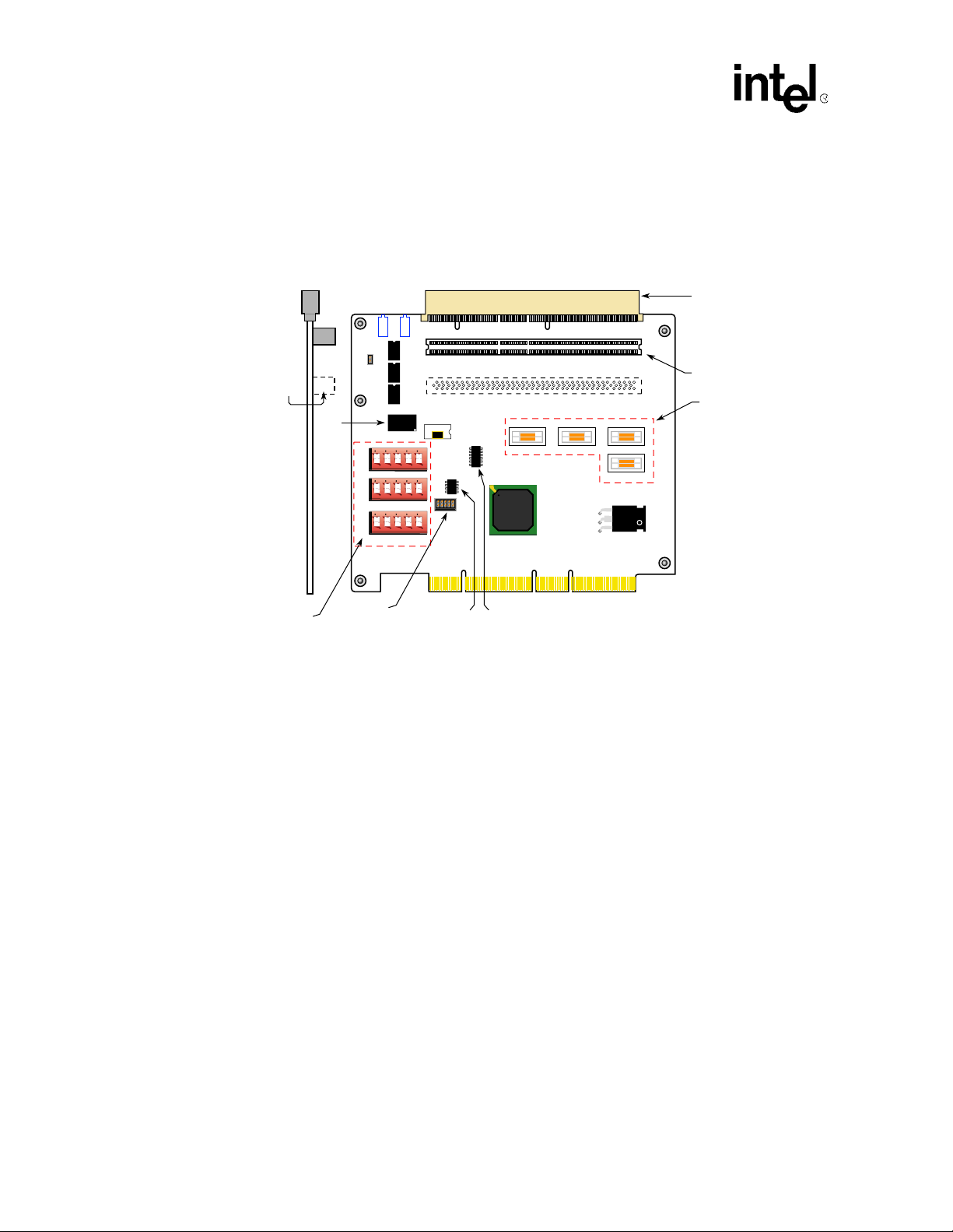
1.3 Major Components
Figure 1 on page6 shows the major components on the DE1B55503.
Figure 1. Major Components
2
1
OPTIONAL
SLOT
Parallel
ROM
Initialization
Switches
1.3.1 Connectors
J8
J21
J20
J9
JTAG
Connector
L2
L1+
E9
E8
E7
1 2 3 4 5
1 2 3 4 5
1 2 3 4 5
SLOT 2
SLOT 1
Y1
E4
OPTIONAL SLOT
J4 J6 J2
E3
E2
21555
Clock Buffer
E5
J1
Serial
ROM
J7
J101
J102
J5
E1
PCI option and slot
PCI option and PICMG
slot
Mictor Connectors for
logic analyzers and
oscilloscopes
A8408-01
• J1 is the 10-pin JTAG connector. See Table A-5 on page 26.
• J7 and J101 (slot 2 and slot 1) are local (secondary bus) PCI option slots.
— J101 (slot 1) can be used for a local processor with the insertion of a PCI Indu strial
Computer Manufacturers Group
(PICMG) Single Board Computer. It is the PCI portion
of the PCI-ISA card edge connector. See Section 1.7 and Section 1.9.
• J102 (secondary bus) is the optional and connector-less slot. The optional slot is for a third
64-bit PCI connector. The through-holes are p rov id ed fo r ins talla ti on o f a local bus conn ect or.
The default build for this board is for two option cards on the local bus. 66MHz operation is
limited to two (2) loads on the PCI bus. All connectors are 64-bit.
• The J2 and J4 Mictor* (scope pod) connectors provide test points for the all the 64-bit S_AD
signals.
• The J5 and J6 Mictor connectors are for other PCI control signals, such as C/BE, REQ, and
GNT. J6 provides test points for parallel ROM data and address lines.
6 21555 PCI-to-PCI Bridge Ev aluation Board User’s Guide
Page 7

Note: See Table A-2 on page 24 for Mictor pinouts.
1.3.2 Switches and Jumper
The DE1B55503 uses a combination of DIP switch, stake-pin and zero ohm resistor jumpers to
control the various configuration options. See Section 1.4, Section 1.5, and Section 1.6 for
information.
• J8 is a single stake pin jumper. See Section 1.5 for information.
• J9, J20, and J21 are five-sw itch switch pack s. The du al-pole switch es are labeled S W1 through
SW5. They control the options at power up such as the d irection of the REQ# and GNT# lines,
the on-board parallel ROM functions, and the enabling of the asynchronous clock options for
the local bus. See Section 1.4 for informat ion.
• Figure 3 on page 10 identifies the location of each configuration jumper.
1.3.3 Devices
• E1 is the voltage regulator that produces the 3.3 and 5 V clamping signal. See Section 1.6.2.
• E2 is the 21555 PCI-to-PCI Bridge.
Introduction
• E3 is the clock buffer.
• E4 is the serial ROM (SROM).
• Y1 is a 33.333 MHz crystal oscillator that can be used for an independent local clock signal.
• E5 is the Parallel ROM. This device is nonvolatile EEPROM. See Section 2.3.2,
“Programming the Flash ROM” on page 18.
• E7, E8, and E9 are address latches.
• E6 (not shown) is the empty socket for attaching a ROM emulator.
• L1 is a LED that indicates the status of the LOO bit (LED On or Off bit) which is switched
through software. This LED can light if jumper J8 is installed.
• L2 is a LED that indicates DE1B55503 5Vdc power status.
21555 PCI-to-PCI Bridge Evaluation Board User’s Guide 7
Page 8
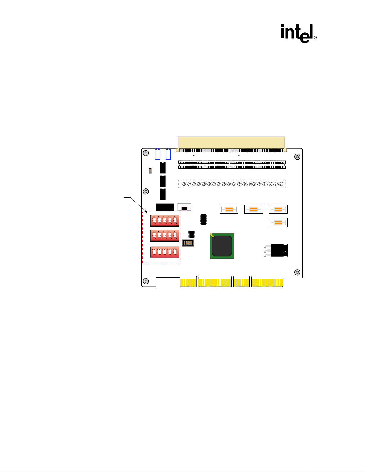
Introduction
1.4 Switch Settings
Figure 2 shows the th ree initialization switch packs, and Table 1 on page 9 gives a high-level
description of each switch. The switches are read at DE1B55503 power up. Further details on the
operation of these swi tches can b e found i n Chapter 3, “Optional Configurations”. Th e switches are
in dual-in-line (DIP) packs designated J9, J20, and J21. Each switch pack contains SW1 through
SW5.
Figure 2. Switches
Initialization
Switches
J8
J21
J20
J9
L2
L1+
E9
E8
E7
E5
1 2 3 4 5
1 2 3 4 5
1 2 3 4 5
SLOT 2
J7
J101
SLOT 1
J102
OPTIONAL SLOT
Y1
E3
E2
E4
J1
J4 J6 J2
J5
21555
E1
A8409-01
8 21555 PCI-to-PCI Bridge Ev aluation Board User’s Guide
Page 9

T a ble 1. DIP Switch Operation
Introduction
Switch
Pack
Switch The Switch Controls Reference Information
SW1, 2, 3 PICMG configurations. (See Chapter 3). Table 10 on page 21
J9
SW4 PR_AD1 strapping option.
SW5 PR_CS to either Flash or optional ROM socket. Table 8 on page 19
SW1 PR_AD2 for SROM operation.
J20
SW2 PR-AD3 for lockout bit control.
SW3 PR_AD4 for synch ronous or async h ronous clock ing.
SW4 PR_AD5 for S_CLKO operation.
SW5 PR_AD6 for Central function selection. Table 12 on page 22
SW#
J21
(1,2,3,4,5)
The REQ/GNT lines for Arbiter control.
1.5 Stake-Pin Jumper
Table 2 shows the configuration and the function of the single stake-pin jumper. J8 enables the
DE1B55503 hot-swap functionality, controls operation of LED L1, and connects the l_stat signal
to a pullup resistor.
Table 2. Stake-Pin Jumper
a
21555 Non Transparent
PCI-to-PCI Bridge User’s
Manual
Table 7 on page 18
Table 14 on page 22
Table 12 on page 22
Table 13 on page 22
Jumper Function
• When removed, the hot-swap functionality is enabled, and L1 will light.
J8
a. No jumper is installed by the Factory default.
• When installed, hot-swap functionality is disabled and the L1 LED is
extinguished.
21555 PCI-to-PCI Bridge Evaluation Board User’s Guide 9
Page 10
Introduction
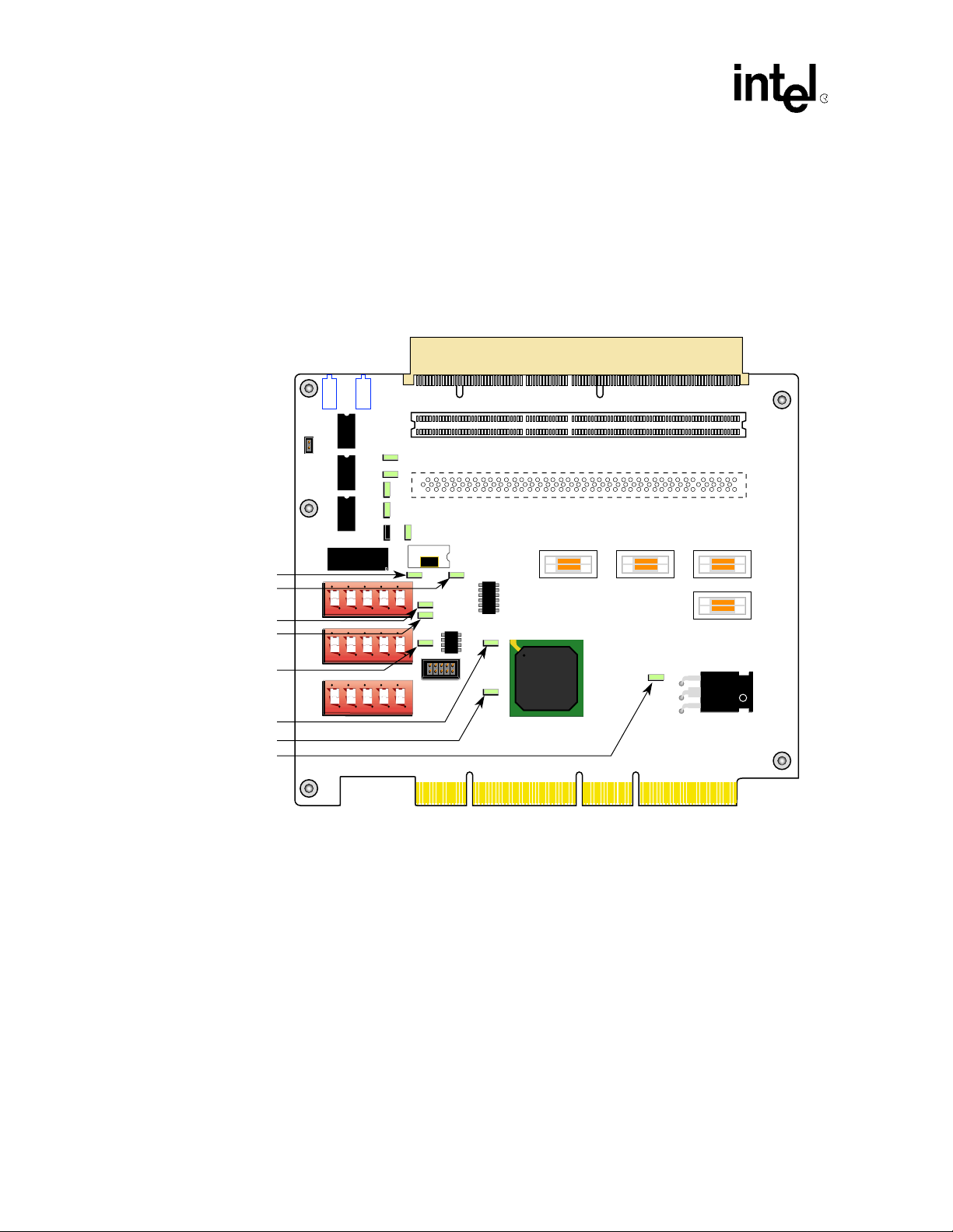
1.6 Resistor Jumpers
Figure 3 shows the lo cation of the zero (0) ohm resistor configuration jumpers. They control the
clock configuration and the clamping voltage. To alter the factory configuration of the
DE1B55503, the jumpers must be soldered on or off the DE1B55503 board. See Appendix A,
“Signal and Default Information”.
Figure 3. Jumper Resistors
R93
R100
R73
R66
R68
R65
R97
R95
J8
E5
J21
J20
J9
L2
L1+
E9
R72
E8
R69
E7
R91 R115
1 2 3 4 5
1 2 3 4 5
1 2 3 4 5
R116
R92
SLOT 2
J7
J101
SLOT 1
J102
OPTIONAL SLOT
Y1
E3
E2
E4
J1
J4 J6 J2
J5
21555
E1
A8410-01
10 21555 PCI-to-PCI Bridge Evaluation Boar d User’s Guide
Page 11

1.6.1 Clock Configuration
Table 3 describes the resistor jumpers to install that connect p_clk and s_clk_o to the Mictor
connectors. To improve signal integrity and minimize noise, these signals are not wired to the
Mictor connectors. Resistor jumpers also control the selection of clock signals. See Figure 3 on
page 10 for the resistor jumper locations. See Table A-3 on page 24 for Mictor pinouts.
Table 3. Clock Configuration Jumpers
Clock Source Installed Removed
Introduction
Use the s_clk_o signal from the 21555 as the local
clock.
Use the s_clk_i that is the output of the clock buffer
as the local clock.
Use the system slot to drive the 21555 s_clk_i. R68 R73
Use an oscillator as the asynchronous local clock. R93 R65, R68
Use the system slot to provide the local clock. R92, R116, R69 R91, R115, R72
Use the clock buffer to provide the local clock. R91, R115, R72 R92, R116, R69
1.6.2 Clamping Voltage
Table 4 gives the clamping voltage resistor jumper configurations. These jumper resistors
designate the DE1B55503 as a 3.3V or a 5V PCI devi ce. A mix of 3.3 and 5 V cards is no t allowed.
The E1 regulator provides the 3.3V or 5 V clamping voltage for the local bus. The resistor jumpers
connect s_vio to either 3.3V or 5V. Figure 4 on page 12 shows the location of the resistor jumpers.
Table 4. Voltage Clamp
Function Installed Removed
s_vio is 3.3V R95 R97
s_vio is 5V R97 R95
a. Only one jumper resistor (R95 or R97) may be installed at
a time. Installing both or no jumper resistors is not allowed.
R65, R73 R68, R93
R73 R68
a
21555 PCI-to-PCI Bridge Evaluation Board User’s Guide 11
Page 12

Introduction
1.7 Secondary Slot Numbering and IDSEL Mapping
Figure 4 gives the bus slot numbering. Table 5 shows how a Product Nam e numbers the Local
slots in response to a Type 0 or Type 1 configuration cycle. The local bus lines s_ad<24> and
s_ad<31:28> are used as local Initilization Device Select (IDSEL) lines.
Figure 4. Local PCI Slot Numbering
PCI option and slot
Device 20/Zero (0)
PCI option and PICMG
slot - Device 13/13
Device 8/8
Device None/17
OPTIONAL
SLOT
2
L2
L1+
E9
J8
1
E8
E7
E5
1 2 3 4 5
J21
1 2 3 4 5
J20
1 2 3 4 5
J9
Y1
E4
J1
SLOT 2
SLOT 1
OPTIONAL SLOT
E3
E2
21555
J7
J101
J102
J4 J6 J2
J5
E1
The 21555 cannot respond to Type 1 but does respond to Type 0 configuration cycles. During a
Type 0 configuration from a Local processor in the PICMG slot, the numbers change so that J7 is
counted one way but reflected as zero the other way.
Table 5. Slot and IDSEL Mapping
Physical Connector
Numbering
J7 (Slot 2) S_AD31 20 zero (0)
J102 (Opt. Slot) S_AD24 8 8
J101 (Slot 1) S_AD29 13 13
E2
(21555)
A8411-01
Device Configuration Numbering
IDSEL Lines Type 1 Type 0
S_AD28 (no response) 17
12 21555 PCI-to-PCI Bridge Evaluation Boar d User’s Guide
Page 13

1.8 Interrupt Routing
Table 6 shows the ORing of interrupts. 12 interrupts are connected to each of three secondary bus
PCI slots but four (4) interrupts are driven to the card edge. The 12 incoming interrupts must be
combined. Interrupt ORing is in accordan ce with the PCI-to-PCI Bridge Ar chitectur e Specification
revision 1.1.
Table 6. Interrupt ORing
Introduction
Device Number
5
(Optional slot J101)
6
(PICMG slot J101)
7
(Top slot J7)
Interrupt Pin on
Device
INTA#
INTB#
INTC#
INTD#
INTA#
INTB#
INTC#
INTD#
INTA#
INTB#
INTC#
INTD#
Interrupt Pin on Board
Connector
INTB#
INTC#
INTD#
INTA#
INTA#
INTB#
INTC#
INTD#
INTD#
INTA#
INTB#
INTC#
21555 PCI-to-PCI Bridge Evaluation Board User’s Guide 13
Page 14

Introduction
1.9 Typical Configurations
Figure 5 shows the DE1B55503 with one local bus option card. The option card can be either
32-bit or 64-bit.
Figure 5. DE1B55503 with One Local Bus Option Card
L2
L1+
J8
ADD-IN CARD
J7
1 2 3 4 5
1 2 3 4 5
1 2 3 4 5
21555
A8412-01
14 21555 PCI-to-PCI Bridge Evaluation Boar d User’s Guide
Page 15

Figure 6 shows the DE1B55503 with two local bus option cards.
Figure 6. DE1B55503 with Two Local Bus Option Cards
L2
L1+
Introduction
ADD-IN CARD
J7
1 2 3 4 5
1 2 3 4 5
1 2 3 4 5
21555
A8413-01
21555 PCI-to-PCI Bridge Evaluation Board User’s Guide 15
Page 16

Page 17

Operations and Installation 2
This chapter provides DE1B555 03 specificati ons and informati on about the hardwa re and software
requirements for using the DE1B55503. It also describes how to install the DE1B55503.
2.1 Specifications
This sections describes some overall specifications for the DE1B55503 board:
Physical dimensions:
• Height: 15.2 cm (6.0 in)
• Width: 17.8 cm (7.0 in)
Power requirements:
• DC amps @ 5 V: 2 A (maximum)
• On Board 3.3V regulator for S_VIO and Vdd 5A (Maximum)
2.2 Hardware Requirements
To operate the DE1B55503, the following equipment is needed:
• A computer system equipped with PCI option slots.
• A PCI expansion slot on the motherboard that is equipped for the 5V PCI environment.
• PCI option cards used to create the local subsystem.
• An optional local processor to control the subsystem. Install the local processor in any of the
three PCI slots. The top PCI slot is configurable as a PICMG (PCI Industrial Computer
Manufacturers Group) CPU slot.
2.3 Software Requirements
The DE1B55503 is shipped with the Serial ROM (SROM) and parallel ROM programmed. The
factory program prints a 21555 banner to the screen during system boot.
The DE1B55503 kit provides DOS utilities that can be used to configure the program in the SROM
and parallel ROM. The diskettes included in the DE1B55503 kit contain:
• PVIEW.EXE to read all PCI configuration space registers.
• CDEBUG, a version of DOS DEBUG that reads memory locations directly.
• DOS4GW.EXE is a DOS32 extender. It must be in the same directory when running the
utilities.
• DBFLASH.EXE an executable utility for erasing and updating the flash ROM memory.
21555 PCI-to-PCI Bridge Evaluation Board User’s Guide 17
Page 18

Operations and Installation
• MSKROM.EXE an executable utility for programming the SROM.
• The software diskettes are standard 3.5 inch floppy disks. Follow the installation procedure
printed on the inside of the shipping package. Be certain that the target system meets the
minimum system requirements.
2.3.1 Programming the SROM
To program the SROM on the DE1B55503, use the MKSROM.EXE utility. Use a text editor to
create an ASCII data file.
MSKSROM file.dat
Where: MSKROM Executes the MSKROM utility.
file.dat Specifies the file to load into the SROM.
To program a blank SROM:
1. Set SW1 and S W2 to “down” during initialization of the system.
2. After the system initializes, toggle SW1 to “up”.
3. Use the MKSROM.EXE utility. For example:
mksrom.exe sromfile.dat
4. Set SW2 to “up” position and reboot system .
Table 7 shows the two SROM enable and lockout switches.
Table 7. Switch Operation for SROM programming
Switch
Pack
J20
Switch
SW1
SW2
Switch
Down
SROM
Output
disabled
No lockout
(debug)
Switch Up Description
SROM
Output
enabled
Lockout
(normal
operation)
The initialization is read from the SROM on
pr_ad<2>:sr_do
Controls the primary lockout bit Reset Value on pr_ad<3>
2.3.2 Programming the Flash ROM
Dbflash.exe is an MSDOS based program that allows the flash ROM attached to the 21555 to be
erased and updated with new images. When dbflash.exe is run on a system that has a 21555
installed on the PCI bus, the program will scan all the PCI buses looking for the 21555 component.
When found, the program will identify the 21555’s PCI location and start the update process that
was selected on the command line.
18 21555 PCI-to-PCI Bridge Evaluation Boar d User’s Guide
Page 19

2.3.2.1 Board Setup
Table 8 gives the DE1B55503 switch configuration for using the DBFLASH.EXE utility.
Table 8. Switch Operation for FLASH programming
Operations and Installation
Switch
Pack
J9 SW5 ROM Socket pr_cs
a. Default configuration.
Switch Switch Down Switch Up
2.3.2.2 Running DbFlash.exe
Make sure that both DBFLASH.EXE and DOS4GW .EXE ar e in the same directory or environment
path. The user must specify the flash block to update and the new image to use. The following will
flash image ‘NewRomImage.bin’ into block zero (0) of the 21554 expansion ROM. During the
next boot of the PC, the BIOS will find this image in the ROM.
Dbflash /b0 NewRomImage.bin
If the BIOS has a PCI compliant Expansion ROM header, the image is loaded and executed by the
system BIOS during POST. For more information, read the PCI Local Bus Specification Revision
2.3.
Dbflash /bx image.bin
Where: Dbflash Runs the dbflash utility from the current directory.
/bx
image.bin
Specifies the starting block to write the program into.
If x=e then all blocks will be erased.
This is the name of the file to load. The file must be in the current directory or
folder. If image is larger than 1 block, the program will continue into the next
block until the entire image is loaded.
a
Program and access
memory using
DBFLASH.EXE.
Description
Enables DBFLASH access to the ROM
Socket or to the flash memory. See
Figure 1 on page 6.
Note: Any other application software is the responsibility of the user.
2.4 Installation Procedure
Figure 2 on page 8 shows the location of components referred to in this section. Follow these steps
to install the DE1B55503:
1. Power down the host system that will contain the DE1B55503.
2. Place the motherboard and the associated support devices on a work bench to allow testing of
the DE1B55503.
3. Before applying power, verify that the DIP switches are set to the desired positions. (The DIP
switch positions are only read during system power up.)
4. Insert the card edge of the DE1B55503 into a PCI slot.
5. Load up the DE1B55503 with the PCI option cards to be tested. Either the 5V or universal
type PCI cards can be installed but card types cannot be mixed. There are two (2) pro vided slot
21555 PCI-to-PCI Bridge Evaluation Board User’s Guide 19
Page 20

Operations and Installation
connectors and one (1) connector-less slot. Section 1.9, “Typical Configurations” on page 14
shows examples of typical PCI configurations.
6. Apply power to the system.
7. Verify the auto-configuration of the 21555 and other options.
a. If the on-board ROM is preloaded the 21555 banner displays.
b. Verify that system BIOS or firmware detects and configures the 21555.
c. To verify the loading of the SROM, run the MKSROM utility without an SROM file as an
input. See Section 2.3.1, “Programming the SROM” on page 18.
8. PCI bus data, address, and control signals are monitored by connecting a logic analyzer to
Mictor connectors J2, J4, J5, and J6. See Appendix A, “Signal and Default Inform atio n”
2.5 Interrupt Routing
Table 9 shows the ORing of interrupts. A total of 12 interrupts are connected to each of three
secondary bus PCI slots but fou r i nterru pt s are driven to t he card ed ge. The 12 incoming interrupts
must be combined. Interrupt ORing is in accordance with the PCI-to-PCI Bridge Architecture
Specification V2.x.
In accordance with the PCI Bridge Architecture Specification, the interrupts of the devices on the
secondary slots are wire ORed and routed to PCI fingers of the DE1B55503.
Table 9. Interrupt ORing
Device Number
5
(Optional Slot J101)
6
(PICMG slot J101)
7
(Top slot J7)
Interrupt Pin on
Device
INTA#
INTB#
INTC#
INTD#
INTA#
INTB#
INTC#
INTD#
INTA#
INTB#
INTC#
INTD#
Interrupt Pin on Board
Connector
INTB#
INTC#
INTD#
INTA#
INTA#
INTB#
INTC#
INTD#
INTD#
INTA#
INTB#
INTC#
20 21555 PCI-to-PCI Bridge Evaluation Boar d User’s Guide
Page 21

Optional Configurations 3
3.1 PICMG Configuration
This section describes how to configure the DE1B55503 to have a Single Board Computer (SBC)
with a PCI interface as defined in the PICMG PCI-ISA Interface Specification. See Section 1.3.1,
“Connectors” on page 6.
The DE1B55503 can have an intelligent subsystem installed that supports the local bus. The
intelligent subsystem is architecture independent. The 21555 can interface to any intelligent
subsystem that has a PCI interface. Connector J101 can accept an intelligent controller and operate
in the PICMG mode. See Figure 2 on page 8.
Table 10 gives the switch configuration to enable PICMG mode operation.
T able 10. J9 PICMG Switches
Switch
Pack
J9
a. J9 positions SW1, SW2, and SW3 must be down for normal PCI operation. The switches define where the RESET,
Switch Switch Down
SW1 PICMG slot DB66 Secondary reset originates
SW2
SW3 PICMG PCI (S_PME#)
ID-SEL, and PME originate.
PICMG
(becomes GNT2)
a
Switch Up Description
PCI
(S_AD24 becomes DSEL)
S_AD24 (IDSEL) originates
Table 11 identifies the zero ohm resistors to remove or install for the s yst em sl ot to act as the clock
source. See Figure 3 on page 10. To operate an SBC controller on the local bus, the clock s mus t be
routed accordingly.
Table 11. Clock Routing Zero Ohm Resistors
Function Installed Removed
System slot drives s_clk_i on the 21555 R68 R73, R65
System slot provides local clock R92, R116, R69 R91, R115, R72
3.2 Central Function and Arbiter Control
T able 12 on page 22 shows the configuration of the DE1B55503 for internal or external arbitratio n.
Arbiter control can be programmed on the evaluation board by switching SW1 J21.
• In one configuration, the internal arbitration logic of the 21555 is the central function.
21555 PCI-to-PCI Bridge Evaluation Board User’s Guide 21
Page 22

Optional Configurations
• In the other configuration, the central function is controlled by the intelligent subsys tem
through the J1 connector.
T a ble 12. External Arbiter Switch Option
Switch
Pack
J20 SW5
J21 SW1
Switch Switch Down Switch Up Description
Enable the 21555
as central arbiter
Disable the 21555
as central arbiter
System slot (J102) as
Central Function
System slot (J102) as
external arbiter.
Central Function Mode(pr_ad<6>)
Disable 21555 arbiter.
Table 13 shows how the req# and gnt # lines must be configured for PICMG operation.
Table 13. J21 Switch Operations for Central Function and Arbiter Control
Switch
Pack
J21
Switch
SW2 req#0 PICMG GNT becomes slot grant req=req
SW3 gnt#0 PICMG REQ becomes slot grant gnt=gnt
SW4 req#1 REQ1 from PICMG slot REQ1 from drawbridge
SW5 gnt#1 GNT1 from PICMG slot GNT1 from drawbridge
Request/
Grant
Switch Do wn
System slot (J102) as arbiter
3.3 Asynchronous Clocking
Table 14 shows how to configure the J20 switches for synchronous or asynchronous operations of
the local bus. If the PICMG slot is the source of the clocks, the resistor strapping options must be
followed as described in Section 3.1. In addition, J20 SW3 must be set for asynchronous clocking
and s_clk_o needs to be disabled from the 21555.
Switch Up
21555 as arbiter
Table 14. Switch Operations for Synchronous or Asynchronous Clock Control
Switch
Pack
J20
22 21555 PCI-to-PCI Bridge Evaluation Boar d User’s Guide
Switch Switch Down Switch Up Description
SW3
SW4 Disable 21555 (s_clk_o) Enable 21555 (s_clk_o)
Synchronous host and
local clock domains
Asynchronous host and
local clock domains
Selects synchronous or
asynchronous operation.
(pr_ad<4>)
s_clk_o
(pr_ad<5>)
Page 23

Signal and Default Information A
A.1 J2 J4, J5, and J6 Connector Pinouts
Table A-1 gives the Mictor connectors pin assignment and DE1B55503 schematic signal names.
See Figure 1 on p age 6 for the location of this connector.
Table A-1. J2 Connector Secondary AD Signals
Schematic
Signal Name
+5V 1 2 SCL
GND 3 4 SDA
S_CLK0_2
CLK
S_AD63 7 8 S_AD47
S_AD62 9 10 S_AD46
S_AD61 11 12 S_AD45
S_AD60 13 14 S_AD44
S_AD59 15 16 S_AD43
S_AD58 17 18 S_AD42
S_AD57 19 20 S_AD41
S_AD56 21 22 S_AD40
S_AD55 23 24 S_AD39
S_AD54 25 26 S_AD38
S_AD53 27 28 S_AD37
S_AD52 29 30 S_AD36
S_AD51 31 32 S_AD35
S_AD50 33 34 S_AD34
S_AD49 35 36 S_AD33
S_AD48 37 38 S_AD32
Mictor
Pin Number
56
Mictor
Pin Number
Schematic
Signal Name
S_CLK0_3
CLKB
21555 PCI-to-PCI Bridge Evaluation Board User’s Guide 23
Page 24

Signal and Default Information
Table A-2 gives the Mictor connectors pin assignment and DE1B55503 schematic signal names.
T able A-2. J4 Pin Assignments
Schematic
Signal Name
+5V 1 2 SCL
GND 3 4 SDA
S_CLK0_2
CLK
S_AD31 7 8 S_AD15
S_AD30 9 10 S_AD14
S_AD29 11 12 S_AD13
S_AD28 13 14 S_AD12
S_AD27 15 16 S_AD11
S_AD26 17 18 S_AD10
S_AD25 19 20 S_AD9
S_AD24 21 22 S_AD8
S_AD23 23 24 S_AD7
S_AD22 25 26 S_AD6
S_AD21 27 28 S_AD5
S_AD20 29 30 S_AD4
S_AD19 31 32 S_AD3
S_AD18 33 34 S_AD2
S_AD17 35 36 S_AD1
S_AD16 37 38 S_AD0
Mictor
Pin Number
56
Mictor
Pin Number
Schematic
Signal Name
S_CLK0_3
CLKB
Table A-3 gives the Mictor connectors pin assignment and DE1B55503 schematic signal names.
T able A-3. J5 CBE, REQ, and GNT
Schematic
Signal Name
+5V 1 2 SCL
GND 3 4 SDA
S_CLK0_2
CLK
S_CBE7
S_CBE6 910S_GNT8
S_CBE5 11 12 S_GNT7
S_CBE4 13 14 S_GNT6
S_CBE3 15 16 S_GNT5
S_CBE2 17 18 S_GNT4
S_CBE1 19 20 S_GNT3
S_CBE0 21 22 S_GNT2
24 21555 PCI-to-PCI Bridge Evaluation Boar d User’s Guide
Mictor
Pin Number
56
78S_REQ0
Mictor
Pin Number
Schematic
Signal Name
S_CLK0_3
CLKB
Page 25

Table A-3. J5 CBE, REQ, and GNT
Signal and Default Information
Schematic
Signal Name
S_REQ8 23 24 S_G NT1
S_REQ7 25 26 S_G NT0
S_REQ6 27 28 S_M 66ENA
S_REQ5
S_REQ4 31 32
S_REQ3
S_REQ2
S_REQ1
Mictor
Pin Number
29 30 S _PNE
33 34 S_CLKI
35 36 SCLK_O
37 38
Mictor
Pin Number
Schematic
Signal Name
Table A-4 gives the Mictor connectors pin assignment and DE1B55503 schematic signal names.
Table A-4. J6, Parallel ROM and Control
Schematic
Signal Name
+5V 1 2 SCL
GND 3 4 SDA
S_CLK0_2
CLK
PR_AD7 7 8 S_FRAME
PR_AD6 9 10 S_IRDY
PR_AD5 11 12 S_DEVSEL
PR_AD4 13 14 S_TRDY
PR_AD3 15 16 S_STOP
PR_AD2 17 18 S_PAR
PR_AD1 19 20 S_SERR
PR_AD0 21 22 S_PERR
DB_SAC5 23 24 S_REQ64
PR_CS 25 26 S_ACK64
PR_CLK 27 28 S_PAR54
PR_ALE 29 30
PR_RD
PR_WR 33 34 PICMG_RST
Mictor
Pin Number
56
31 32 S_RST
35 36 L_STAT
37 38 P_ENUM
Mictor
Pin Number
Schematic
Signal Name
S_CLK0_3
CLKB
21555 PCI-to-PCI Bridge Evaluation Board User’s Guide 25
Page 26

Signal and Default Information
A.2 JATAG Connector Pinout
Table A-5 gives the pin assignments between the DE1B55503 schematic and the ten-pin JTAG
connector. See Figure 1 on page 6 for the location of this connector.
T able A-5. J1 JATAG Connector
Schematic
Number
TRST
TDI 3 4 GND
TD0 5 6 GND
TMS 7 8 GND
TCK 9 10 GND
Mictor
Pin Number
12GND
Mictor
Pin Number
Schematic
Number
A.3 Factory Default Switch and Jumper Configuration
The DE1B55503 is configured at the factory for normal or typical operation.
• J8, the stake pin jumper, is not installed
• Table A-6 gives the factory configuration for the switch pack switches.
T able A-6. Switch Pack Factory Defaults
Switches on Are set at the Factory.
J9 all switches are in the up position.
J20
J21 all switches are in the up position.
SW1, SW2, and SW4 are n the up position
SW3 and SW5 are down.
a
a. The UP position leaves the switch lever pointing towards the
local option sockets.
• Table A-7 gives the configuration of the zero-ohm resistor jumpers.
Table A-7. Resistor Jumper Factory Defaults
Resistor
Jumper
R65 IN R92 OUT
R68 OUT R93 OUT
R69 OUT R95 OUT
R72 IN R97 IN
R73 IN R115 IN
R91 IN R116 OUT
26 21555 PCI-to-PCI Bridge Evaluation Boar d User’s Guide
In/Out
Resistor
Jumper
In/Out
 Loading...