

Page 1

Intel® Stratix® 10 DX FPGA
Development Kit User Guide
Subscribe
Send Feedback
UG-20255 | 2020.11.16
Latest document on the web: PDF | HTML
Page 2

Contents
Contents
1. Getting Started............................................................................................................... 4
1.1. About this Document..............................................................................................4
1.2. Installing the Intel Quartus® Prime Pro Edition Software............................................. 4
1.2.1. Activating Your License...............................................................................4
1.3. Downloading the Board Package.............................................................................. 4
1.4. Installing the Driver for Intel FPGA Download Cable II................................................ 5
2. Development Kit Overview..............................................................................................6
2.1. Supported Features............................................................................................... 7
2.2. Recommended Operating Conditions........................................................................ 7
2.3. Handling the Board................................................................................................ 8
3. Power Up the Development Kit....................................................................................... 9
3.1. Default Switch Settings.......................................................................................... 9
3.2. Connectors and LEDs............................................................................................12
3.3. Performing Board Restore through Board Test System (BTS) .....................................13
3.4. Controlling On-board Clock....................................................................................14
4. Board Test System (BTS).............................................................................................. 15
4.1. Preparing the Development Kit.............................................................................. 16
4.2. Running the Board Test System............................................................................. 16
4.3. Using the Board Test System.................................................................................17
4.3.1. Configure Menu....................................................................................... 17
4.3.2. Sys Info Tab............................................................................................18
4.3.3. GPIO Tab................................................................................................ 19
4.3.4. QSFP Tab................................................................................................20
4.3.5. Component DDR4 CH0 Tab........................................................................23
4.3.6. Component DDR4 CH1 Tab........................................................................24
4.3.7. DDR4 DIMM CH0 Tab................................................................................26
4.3.8. DDR4 DIMM CH1 Tab................................................................................27
4.3.9. Power Monitor......................................................................................... 29
4.3.10. Clock Controller..................................................................................... 30
4.4. Smart VID Setting............................................................................................... 32
5. Development Kit Hardware and Configuration.............................................................. 34
5.1. FPGA Configuration.............................................................................................. 34
5.2. Programming the FPGA Over Intel FPGA Download Cable.......................................... 34
5.3. Configuration Modes.............................................................................................35
5.3.1. Avalon Streaming Interface x8 Mode.......................................................... 35
5.3.2. JTAG Mode..............................................................................................40
6. Document Revision History for Intel Stratix 10 DX FPGA Development Kit User Guide..42
A. Development Kit Components....................................................................................... 43
A.1. Components Overview..........................................................................................44
A.2. Power, Thermal, and Mechanical Considerations....................................................... 47
A.2.1. Power Guidelines..................................................................................... 47
A.2.2. Thermal Requirements............................................................................. 53
A.2.3. Mechanical Requirements..........................................................................54
Intel® Stratix® 10 DX FPGA Development Kit User Guide
2
Send Feedback
Page 3

Contents
A.3. Clock Circuits...................................................................................................... 56
A.4. Memory Interface................................................................................................ 58
A.5. PCIe Interface..................................................................................................... 59
A.6. UPI Interface...................................................................................................... 59
A.7. Transceiver Signals: PCIe and UPI Interface............................................................ 60
A.8. SlimSAS Connector.............................................................................................. 63
A.9. QSFP Network Interface........................................................................................64
A.9.1. Dual Port Controller .................................................................................65
A.10. I2C Interface..................................................................................................... 66
A.11. QSPI Flash Memory............................................................................................ 67
A.11.1. Configuration QSPI Flash Memory.............................................................67
A.11.2. NIOS QSPI Flash Memory........................................................................67
B. Safety and Regulatory Information...............................................................................69
B.1. Safety Warnings.................................................................................................. 69
B.2. Safety Cautions................................................................................................... 71
C. Compliance and Conformity Information...................................................................... 73
Send Feedback
Intel® Stratix® 10 DX FPGA Development Kit User Guide
3
Page 4
UG-20255 | 2020.11.16
Send Feedback
1. Getting Started
1.1. About this Document
This document provides comprehensive guidelines for designing with Intel® Stratix
10 DX FPGA Development Kit. It covers information about the software installation,
board components, and configuration.
Table 1. Ordering Information
Product Ordering Code Device Part Number
Intel Stratix 10 DX FPGA Development Kit
(Production version)
1.2. Installing the Intel Quartus
The Intel Quartus® Prime Pro Edition software includes everything you need to design
for Intel Stratix 10 FPGA from design entry and synthesis to optimization, verification,
and simulation. For more information about downloading the Intel Quartus Prime Pro
Edition software, refer to the Download Center for Intel FPGAs.
1.2.1. Activating Your License
Before using the Intel Quartus Prime Pro Edition software, you must activate your
license. If you already have a licensed version installed, you can use that license file
with this development kit. Otherwise, follow these steps:
1. Log into your My Intel account.
2. Click on the Intel FPGA Self Service Licensing Center.
3. Locate the serial number printed on the side of the development kit box below the
bottom bar code. The number consists of alphanumeric characters and does not
contain hyphens.
4. On the Intel FPGA Self Service Licensing Center page, click the Find it with
your License Activation Code link.
5. In the Find/Activate Products dialog box, enter your development kit serial
number and click Search.
DK-DEV-1SDX-P-A 1SD280PT2F55E1VG
®
Prime Pro Edition Software
®
1.3. Downloading the Board Package
Download the appropriate board package for your Intel Stratix 10 DX FPGA
Development Kit from the Intel FPGA Development Kits webpage. Unzip the package.
Intel Corporation. All rights reserved. Agilex, Altera, Arria, Cyclone, Enpirion, Intel, the Intel logo, MAX, Nios,
Quartus and Stratix words and logos are trademarks of Intel Corporation or its subsidiaries in the U.S. and/or
other countries. Intel warrants performance of its FPGA and semiconductor products to current specifications in
accordance with Intel's standard warranty, but reserves the right to make changes to any products and services
at any time without notice. Intel assumes no responsibility or liability arising out of the application or use of any
information, product, or service described herein except as expressly agreed to in writing by Intel. Intel
customers are advised to obtain the latest version of device specifications before relying on any published
information and before placing orders for products or services.
*Other names and brands may be claimed as the property of others.
ISO
9001:2015
Registered
Page 5
<package rootdir>
board_design_files
demos
documents
examples
factory_recovery
1. Getting Started
UG-20255 | 2020.11.16
Figure 1. Directory Structure
Table 2. Directory Description
Directory Content Description
board_design_files
demos
documents
examples
factory_recovery
Contains schematic, layout, assembly, and bill of material board design files. Use
these files as a starting point for a new prototype board design.
Contains demonstration applications when available.
Contains documentation.
Contains sample design files for this development kit.
Contains the original data programmed onto the board before shipment. Use this
data to restore the board to its original factory settings.
1.4. Installing the Driver for Intel FPGA Download Cable II
The development board includes integrated Intel FPGA Download Cable circuits for
FPGA programming. However, for the host computer and board to communicate, you
must install the Intel FPGA Download Cable II driver on the host computer.
Installation instructions for the Intel FPGA Download Cable II driver for your operating
system are available on the Cable and Adapter Drivers Information webpage.
Send Feedback
Intel® Stratix® 10 DX FPGA Development Kit User Guide
5
Page 6
3D
UPI_1
TX
x4
QSFP-2
QSFP-1
25G x4 or 56G x2
x4
25G x4 or 56G x2
x20
TX
x20
TX
x20
RX
x20
RX
SlimSAS x2
UPI/PCle EP/RP
UPI_1RXUPI_2TXUPI_2
RX
SlimSAS x2
UPI/PCle EP/RP
X72
X72
X72
QSPI
2Gb Flash
USB
PHY
USB
JTAG HDR
Current
Sense
JTAG
JTAG
AVST x8
QSPI x4
Config
GPIO
Temp
Sense
PWR in
CTRL
Aux_2
12V
Voltage
Regulators &
Discharge CKT
NIOS
FLASH
Clock
I2C
Pwr Seq CTRL
I2C
Current Sense
Inputs
Temp Diodes
All Clocks
+12V
+12V from PCle
Gold Finger
Voltage Sense
Inputs
All
Voltages
Intel
MAX 10
System
Control
DDR4
512Mx16 X5
DDR4_CH1
DDR4
512Mx16 X5
DDR4_CH0
X72
2K
2L
2M
2N
2J
2I
3I
3D
E-Tile
9A
3C
3B
3A
2A
RX
AVSTx8
TX
x16
x16
RX
TX
x20
x20
2B
2C
2F
3J
3K
3L
3H
P-Tile
11B
P-Tile
11C
P-Tile
10A
P-Tile
10B
UPI_0
RX
UPI/PCIe EP/RP
SlimSAS x2
UPI_0
TX
Intel Stratix 10 DX
FPGA Development Kit
DIMM_CH0
DDR4/DDR-T
DIMM_CH1
DDR4/DDR-T
PCIe Gen4 X16 Edge Conn
SDM
UG-20255 | 2020.11.16
Send Feedback
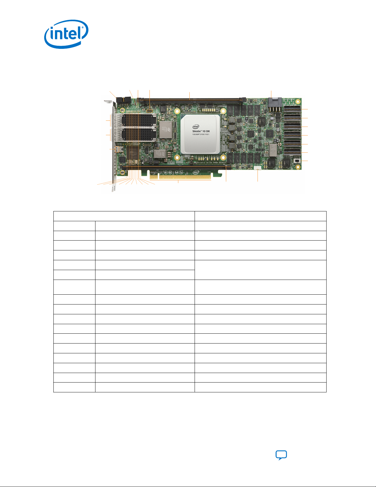
2. Development Kit Overview
The Intel Stratix 10 DX FPGA Development Kit allows you to evaluate the
performance, features, and operation of the Intel Stratix 10 DX device in the F2912
BGA package. It features P-tile transceivers with PCIe Gen4 x16 and Intel Ultra Path
Interconnect (UPI) interfaces and E-tile transceivers with 25Gx4 or 56Gx2 quad small
form-factor pluggable (QSFP) interfaces. It also supports 4xDDR4 x72 channels with
two channels supporting the Intel Optane® DC Persistent memory module.
The UPI functionality is enabled by a combination of the appropriate P-Tile settings
and UPI protocol IP core. The FPGA interface to Intel Optane DC Persistent memory
module requires an Intel memory controller IP core. Both IP cores are available in
Intel Quartus Prime Pro Edition software (additional licensing and enablement may
apply).
Figure 2. Intel Stratix 10 DX FPGA Development Kit Block Diagram
Intel Corporation. All rights reserved. Agilex, Altera, Arria, Cyclone, Enpirion, Intel, the Intel logo, MAX, Nios,
Quartus and Stratix words and logos are trademarks of Intel Corporation or its subsidiaries in the U.S. and/or
other countries. Intel warrants performance of its FPGA and semiconductor products to current specifications in
accordance with Intel's standard warranty, but reserves the right to make changes to any products and services
at any time without notice. Intel assumes no responsibility or liability arising out of the application or use of any
information, product, or service described herein except as expressly agreed to in writing by Intel. Intel
customers are advised to obtain the latest version of device specifications before relying on any published
information and before placing orders for products or services.
*Other names and brands may be claimed as the property of others.
ISO
9001:2015
Registered
Page 7
2. Development Kit Overview
UG-20255 | 2020.11.16
2.1. Supported Features
Table 3. Supported Features
Category Features
• 0.85-0.89V/VID-adjustable VCC core, 2912 pin BGA package
Intel Stratix 10 DX FPGA
FPGA configuration
Programmable clock sources
Transceiver interfaces
Memory interfaces
Communication ports
Buttons, Switches, and LEDs
Heatsink and Fan
Power
Mechanical
• P-Tile transceivers supporting PCIe Gen4 or UPI
• E-Tile transceivers supporting 28Gbps NRZ and 56Gbps PAM4
• Partial reconfiguration support
• CVP configuration support
• 2Gb QSPI Flash
• Storage for one configuration image in flash
• JTAG header for device programming
• Built-in Intel FPGA Download Cable for device programming
• 312.53125 Mhz and 156.25 MHz Differential LVDS for QSFP
• 100 Mhz Differential LVDS for PCIe
• 133 Mhz Differential LVDS for Memory
• 125 Mhz Configuration clock
• 100 Mhz Differential LVDS for IO banks
• PCIe x16 interface supporting Gen4 End-Point mode connected to a x16 PCIe edge
connector (gold edge fingers)
• 2x standard QSFP56 optical module interfaces connected to the E-tile transceivers
• 3x UPI or PCIe interface supporting UPI x20 at 11.2Gbps or PCIe x16 at 16Gbps via
SlimSAS connectors (cables shipped separately)
• Two on-board independent single rank DDR4 x72 (ECC) channels operating at 1200 MHz
(DDR4-2400)
• Two DIMM sockets supporting DDR4 DIMM or Intel’s Optane DC Persistent memory
module
• 2xQSFP28 optical interface port
• JTAG header
• USB (Micro USB) on-board Intel FPGA Download Cable II
• System I2C header
• System Reset Push button
• CPU Reset Push button
• PCIe Reset Push button
• Four dedicated User LEDs
• Link LED of each QSFP28 port to indicate the link and data transceiver
• Two dedicated configuration status LEDs
• Air-cooled heatsink assembly
• Red Over-Temperature Warning LED Indicator
• PCIe input power including required 2x4 AUX power connector
• Blue Power-On LED
• On/Off Slide Power Switch for benchtop operation
• On board power and temperature measurement circuitry
• PCIe standard height form factor
• 4.376” x 10.0” board size
• 2 Slots height with heatsink
2.2. Recommended Operating Conditions
Follow these operating range or limit for different physical parameters:
Send Feedback
Intel® Stratix® 10 DX FPGA Development Kit User Guide
7
Page 8

2. Development Kit Overview
UG-20255 | 2020.11.16
• Ambient operating temperature range: 0°C to 35°C
• Maximum ICC load current: 192 A
• Maximum ICC load transient percentage: 30%
• FPGA maximum power supported by the supplied heatsink/fan: 192 W
2.3. Handling the Board
When handling the board, it is important to observe static discharge precautions.
Caution: Without proper anti-static handling, the board can be damaged. Therefore, use anti-
static handling precautions when touching the board.
Important: This development kit should not be operated in a vibrating environment.
Intel® Stratix® 10 DX FPGA Development Kit User Guide
8
Send Feedback
Page 9

UG-20255 | 2020.11.16
Send Feedback
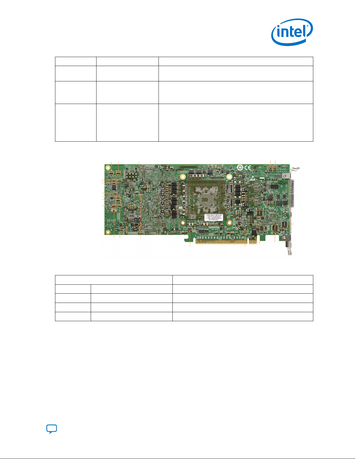
3. Power Up the Development Kit
The Intel Stratix 10 DX FPGA development kit is designed to operate in two modes:
• As a PCIe* add-in card
• Bench-top mode
When operating the card as a PCIe system, insert the card into an available PCIe slot
and connect a 2x4 pin PCIe power cable from the system to power connectors at J42
of the board.
Note: When operating as a PCIe add-in card, the board does not power on unless power is
supplied to J42.
In Bench-top mode, you must supply the board with 240 W of power supply connected
to the power connector J42.
This development kit ships with its switches preconfigured to support the design
examples in the kit. If you suspect that your board may not be correctly configured
with the default settings, refer to the Default Switch and Jumper Settings section of
this chapter.
Follow these instructions:
1. Connect the supplied power supply to an outlet and the DC Power Jack (J42) on
the FPGA board.
Note: Use only the supplied power supply. Power regulation circuits on the board
can be damaged by power supplies with greater voltage.
2. Set the power switch (SW31) to the ON position.
When the board powers up, the blue LED illuminates and the board is ready for use.
The Orange LED (D56) should also illuminate indicating that all the power rails on the
board are good. If the POWER GOOD LED (D56) is not illuminated, it indicates that the
power supply is malfunctioned and the board will not power up.
Note: The standby powers are always present as soon as the AUX power is applied to J42.
Use power switch SW31 to start the board.
3.1. Default Switch Settings
This development kit ships with its switches preconfigured to support the design
examples in the kit. If you suspect that your board may not be correctly configured
with the default settings, refer to the following table to return to its factory settings
before proceeding.
Intel Corporation. All rights reserved. Agilex, Altera, Arria, Cyclone, Enpirion, Intel, the Intel logo, MAX, Nios,
Quartus and Stratix words and logos are trademarks of Intel Corporation or its subsidiaries in the U.S. and/or
other countries. Intel warrants performance of its FPGA and semiconductor products to current specifications in
accordance with Intel's standard warranty, but reserves the right to make changes to any products and services
at any time without notice. Intel assumes no responsibility or liability arising out of the application or use of any
information, product, or service described herein except as expressly agreed to in writing by Intel. Intel
customers are advised to obtain the latest version of device specifications before relying on any published
information and before placing orders for products or services.
*Other names and brands may be claimed as the property of others.
ISO
9001:2015
Registered
Page 10
Table 4. Default Switch Settings
Switch Default Position Description
SW1[1:4] ON/OFF/OFF/X
SW33[1:4] OFF/X/ON/ON
SW2[1:4] ON/ON/ON/ON
3. Power Up the Development Kit
UG-20255 | 2020.11.16
Configuration mode setting bits:
Mode MSEL0 MSEL1 MSEL2
JTAG OFF (Open) OFF (Open) OFF (Open) X
Avalon-ST ON (Close) OFF (Open) OFF (Open) X
JTAG, MAX10, UPI controls:
SW33 ON (Close) OFF (Open)
1 - JTAG Debug
2 - JTAG SOURCE Not used Not used
3 - UPI Mode 2 Sockets 4 Sockets
4 – M10 JTAG EN M10 JTAG Enabled M10 JTAG Disabled
PCIe PRSNT X1/x4/x8/x16 settings:
PCIe PRSNT X1 PCIe PRSNT X4 PCIe PRSNT X8
ON (Close) ON (Close) ON (Close) ON (Close)
JTAG Header (J2)
dedicated for Max10
Normal JTAG (Default)
QSPI_AVST
_SEL
PCIe PRSNT
X16
PCIe Edge connector PERSTn selection:
SW28 ON (Close)
SW27 ON (Close)
SW16 ON (Close)
SW24 ON (Close)
SW17 ON (Close)
SW25 ON (Close)
SW18 ON (Close)
SW26 ON (Close) UPI2 PERSTn selection - FPGA side:
• ON: Endpoint (Default)
• OFF: Root Port
Intel Stratix 10 DX PERSTn selection:
• ON: Endpoint (Default)
• OFF: Root Port
UPI0 PERSTn selection - UPI0 connector side:
• ON: PERSTn from PCIe Edge connector to FPGA
• OFF: PERSTn from FPFA to CPU (Default)
UPI0 PERSTn selection - FPGA side:
• ON: PERSTn from FPGA to CPU (Default)
• OFF: PERSTn from PCIe Edge connector to FPGA
UPI1 PERSTn selection - UPI1 connector side:
• ON: PERSTn from PCIe Edge connector to FPGA
• OFF: PERSTn from FPFA to CPU (Default)
UPI1 PERSTn selection - FPGA side:
• ON: PERSTn from FPGA to CPU (Default)
• OFF: PERSTn from PCIe Edge connector to FPGA
UPI2 PERSTn selection - UPI2 connector side:
• ON: PERSTn from PCIe Edge connector to FPGA
• OFF: PERSTn from FPFA to CPU (Default)
continued...
Intel® Stratix® 10 DX FPGA Development Kit User Guide
10
Send Feedback
Page 11
SW25
SW20
SW18
SW20
SW27
SW16
SW19
S4 SW17
SW14
S3
SW28
SW2
SW33
SW1
S1 S2
SW24 SW26
3. Power Up the Development Kit
UG-20255 | 2020.11.16
Switch Default Position Description
• ON: PERSTn from FPGA to CPU (Default)
• OFF: PERSTn from PCIe Edge connector to FPGA
PCIe REFCLK source selection:
SW14 ON (Close)
SW31 ON (Close) or OFF (Open)
•
ON: 100MHz REFCLK internal generated
•
OFF: 100MHz REFCLK from PCIe Edge Connector (Default)
Power switch:
• ON: Turn on power (set to this position for use in PCIe slot)
• OFF: Turn off power
This switch must be ON when the card is plugged into a PCIe slot
(with 2x4 Aux power connected) or on the bench with external
Note:
ATX power supply.
Figure 3. Location of Switches and Push Buttons
Table 5. Push Buttons
Push Buttons Descriptions
S1 PCIe Reset Push to reset PCIe bus
S2 MAX10 Reset Push to reset Max10
S3 CPU Reset Push to reset FPGA
S4 USER Push Button Push button for user assigned function
Send Feedback
Intel® Stratix® 10 DX FPGA Development Kit User Guide
11
Page 12
3.2. Connectors and LEDs
J2
J18
J15
CN1
D9 D10 D14 D15 D18 D20 D22 D21 D13 D40
J9
J74
SW31
J65
J55
J41
J40
J39
J38
J42
D57 D56 J17
J73
J24
Figure 4. Location of Connectors and LEDs
Table 6. Connectors
3. Power Up the Development Kit
UG-20255 | 2020.11.16
Connector Description
J2 External JTAG connector For use with Intel FPGA Download Cable
J42 AUX Power connector For external 12V AUX power supply or power adapter
J97 I2C/PMBus connector For accessing the core power controller
J17 I2C connector To access I2C bus
J15 QSFP 1 connector
J18 QSFP 2 connector
CN1 USB connector
J73 DIMM 0 connector For DDR4/DDR-T memory channel 0
J74 DIMM 1 connector For DDR4/DDR-T memory channel 1
J9 PCIe x16 Gold Finger For using the PCIe interface
J38 UPI 1 Transmit For UPI Link 1 connection from FPGA to CPU
J40 UPI 1 Receive For UPI Link 1 connection from CPU to FPGA
J39 UPI 2 Transmit For UPI Link 2 connection from FPGA to CPU
J41 UPI 2 Receive For UPI Link 2 connection from CPU to FPGA
J55 UPI 0 Transmit For UPI Link 0 connection from FPGA to CPU
J65 UPI 0 Receive For UPI Link 0 connection from CPU to FPGA
J24 Fan connector For connecting to the heatsink cooling fan
For using the QSFP interface
For programming FPGA using on-board Intel FPGA
Download Cable
Intel® Stratix® 10 DX FPGA Development Kit User Guide
12
Send Feedback
Page 13
3. Power Up the Development Kit
UG-20255 | 2020.11.16
Table 7. LEDs
LEDs Description
D18 QSFP 1 Link LED for 25G
D20 QSFP 1 Link LED for 10G
D22 QSFP 2 Link LED for 25G
D21 QSFP 2 Link LED for 10G
D9 USER LED 0 Green LED for USER LED 0
D10 USER LED 1 Green LED for USER LED 1
D14 USER LED 2 Green LED for USER LED 2
D15 USER LED 3 Green LED for USER LED 3
D56 POWER GOOD LED
D57 CONFIG DONE LED
D13 MAX10 CONFIG DONE LED
D40 Over Temp LED
D53 POWER LED
Green LED:
• ON: link
• Blinks: Activities
Yellow LED:
• ON: link
• Blinks: Activities
Green LED:
• ON: link
• Blinks: Activities
Yellow LED:
• ON: link
• Blinks: Activities
Yellow LED:
• ON: All power is good
• OFF: Power failure
Green LED:
• ON: FPGA configuration successful
• OFF: FPGA configuration failed
Green LED:
• ON: MAX10 configuration successful
• OFF: MAX10 configuration failed
Red LED:
• ON:
• OFF:
Blue LED:
• ON: Devkit power is on
• OFF: Devkit power is off
3.3. Performing Board Restore through Board Test System (BTS)
The development kit ships with FPGA design examples stored in the QSPI flash device
and pre-programmed Intel MAX® 10 system. If you want to restore the board QSPI
flash with the default factory image, follow these steps:
1. Connect USB cable between CN1 USB connector and your computer.
2. Open Intel Quartus Prime Pro Edition Programmer.
3. Detect JTAG chain and attach factory default image on system Intel MAX 10
device.
4. Select programming options and click Program button.
Send Feedback
Intel® Stratix® 10 DX FPGA Development Kit User Guide
13
Page 14

3.4. Controlling On-board Clock
The clock controller application can change the on-board Si53XX programmable
oscillators to any customized frequency between 0.2 MHz and 800 MHz.
The clock control application (ClockControl.exe) runs as a stand-alone application
and resides in the location <package dir>\examples\board_test_system.
The clock control application communicates with the system Intel MAX 10 device
through either USB port CN1 or 10pin JTAG header J2. The system Intel MAX 10
device controls these programmable clock parts through a two-wire serial bus.
3. Power Up the Development Kit
UG-20255 | 2020.11.16
Intel® Stratix® 10 DX FPGA Development Kit User Guide
14
Send Feedback
Page 15
UG-20255 | 2020.11.16
Send Feedback
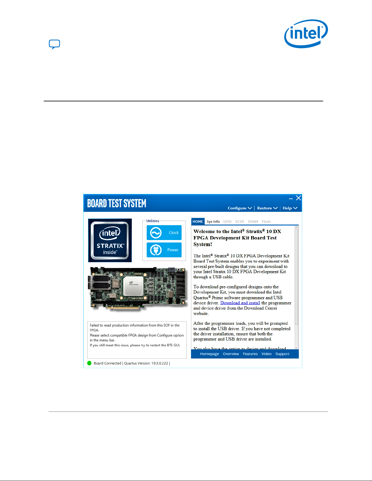
4. Board Test System (BTS)
The Intel Stratix 10 DX FPGA Development Kit includes an application called Board
Test System (BTS) to test the functionality of this board. The BTS provides an easy-touse Graphical User Interface (GUI) to alter functional settings and observe results. You
can use the BTS to test board components, modify functional parameters, observe
performance, and measure power usage.
The BTS communicates over the JTAG bus to a test design running in the Intel Stratix
10 DX FPGA device. You can use the BTS to reconfigure the FPGA with test designs
specific to the functionality that you are testing.
The BTS is also useful as a reference for designing systems.
Figure 5. BTS GUI Home
Intel Corporation. All rights reserved. Agilex, Altera, Arria, Cyclone, Enpirion, Intel, the Intel logo, MAX, Nios,
Quartus and Stratix words and logos are trademarks of Intel Corporation or its subsidiaries in the U.S. and/or
other countries. Intel warrants performance of its FPGA and semiconductor products to current specifications in
accordance with Intel's standard warranty, but reserves the right to make changes to any products and services
at any time without notice. Intel assumes no responsibility or liability arising out of the application or use of any
information, product, or service described herein except as expressly agreed to in writing by Intel. Intel
customers are advised to obtain the latest version of device specifications before relying on any published
information and before placing orders for products or services.
*Other names and brands may be claimed as the property of others.
ISO
9001:2015
Registered
Page 16
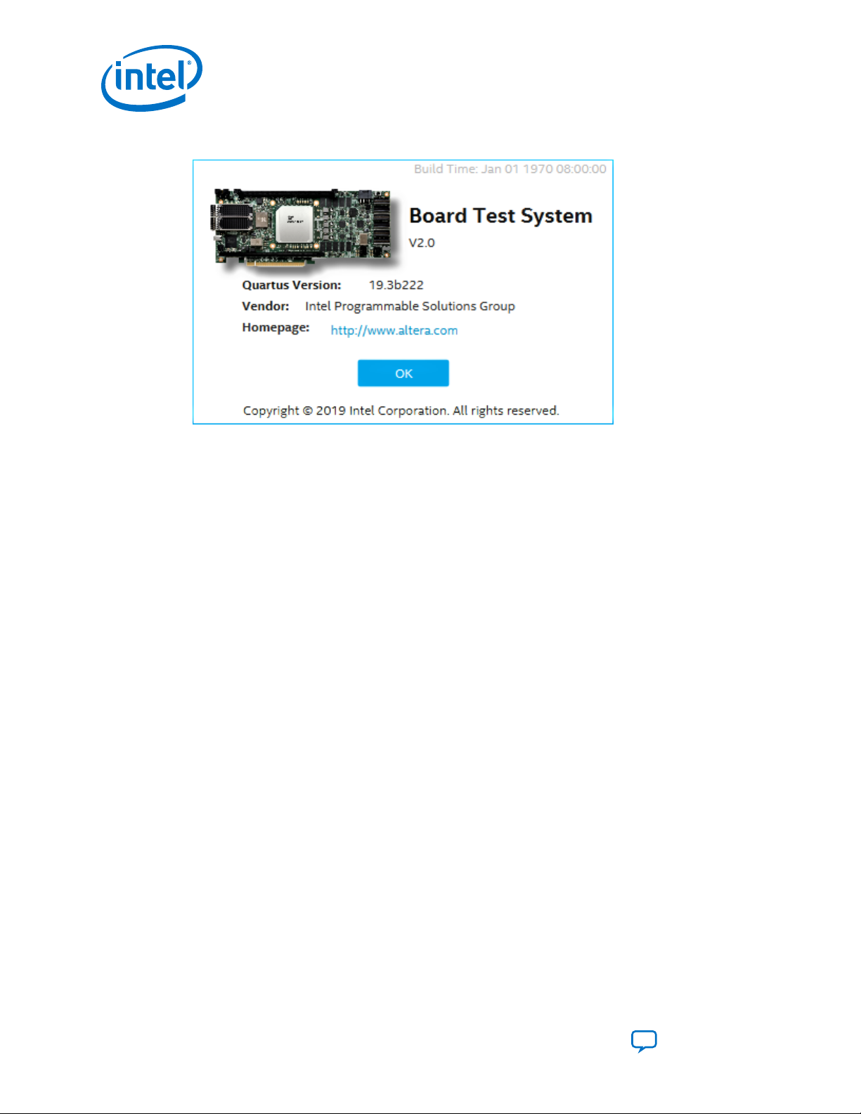
Figure 6. About BTS
4.1. Preparing the Development Kit
4. Board Test System (BTS)
UG-20255 | 2020.11.16
Several designs are provided to test the major board features. Each design provides
data for one or more tabs in the application. The Configure Menu identifies the
appropriate design to download to the FPGA for each tab.
After successful FPGA configuration, an appropriate tab appears that allows you to
exercise the related board features. Highlights appear in the board picture around the
corresponding components.
The BTS communicates over the JTAG bus to a test design running in the FPGA. The
BTS and Power Monitor share the JTAG bus with other applications like the Nios® II
debugger and the Signal Tap II Embedded Logic Analyzer. Because the BTS is designed
based on the Intel Quartus Prime software, be sure to close other applications before
you use the BTS.
The BTS relies on the Intel Quartus Prime software's specific library. Before running
the BTS, open the Intel Quartus Prime software to automatically set the environment
variable $QUARTUS_ROOTDIR. The BTS uses this environment variable to locate the
Intel Quartus Prime library. The version of Intel Quartus Prime software set in the
QUARTUS_ROOTDIR environment variable should be newer than version 14.1. For
example, the Development Kit Installer version 15.1 requires that the Intel Quartus
Prime software 14.1 or later version is installed.
Additionaly, to ensure that the FPGA is configured successfully, you should install the
latest Intel Quartus Prime software that can support the silicon on the development
kit. For this board, Intel recommends installing the Intel Quartus Prime version 19.3
b222.
Refer to the README.txt file under \examples\board_test_system directory.
4.2. Running the Board Test System
With the power to the board turned off, follow these steps:
Intel® Stratix® 10 DX FPGA Development Kit User Guide
16
Send Feedback
Page 17
4. Board Test System (BTS)
UG-20255 | 2020.11.16
1. Connect the USB cable to your PC and the board.
2. Check whether the board switches and jumpers are set according to your
preferences.
3. Turn on the power to the board.
To ensure operating stability, keep the USB cable connected and the board powered on
when running the demonstration application. The BTS cannot run correctly unless the
USB cable is attached and the board is powered on.
To run the BTS, navigate to the <package dir>\examples\board_test_system
directory and run the BoardTestSystem.exe application. A GUI appears, displaying
the application tab corresponding to the design running in the FPGA. If the design
loaded in the FPGA is not supported by the BTS GUI, you will receive a message
prompting you to configure your board with a valid BTS design. Refer to the Configure
Menu on page 17 for configuring your board.
If some design is running in the FPGA, the BTS GUI loads the design file (.sof) in
the image folder to check the current running design in the FPGA. Therefore, the
design running in the FPGA must be the same as the design file in the image folder.
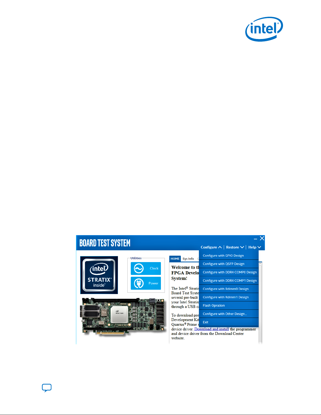
4.3. Using the Board Test System
This section describes each tab in the BTS.
4.3.1. Configure Menu
Use the Configure menu to select the design you want to use. Each design example
tests different board features. Select a design from this menu and the corresponding
tabs become active for testing.
Figure 7. Configure Menu
To configure the FPGA with a test system design, perform the following steps:
Send Feedback
Intel® Stratix® 10 DX FPGA Development Kit User Guide
17
Page 18
4. Board Test System (BTS)
UG-20255 | 2020.11.16
1. On the Configure menu, click the configure command that corresponds to the
functionality you want to test.
2. In the dialog box that appears, click Configure to download the corresponding
design to the FPGA.
When configuration finishes, close the Intel Quartus Prime software GUI if it's already
open. The design begins running in the FPGA. The corresponding GUI application tabs
that interface with the design are now enabled.
Note: If you use the Intel Quartus Prime Programmer for configuration rather than the BTS
GUI, you may need to restart the GUI.
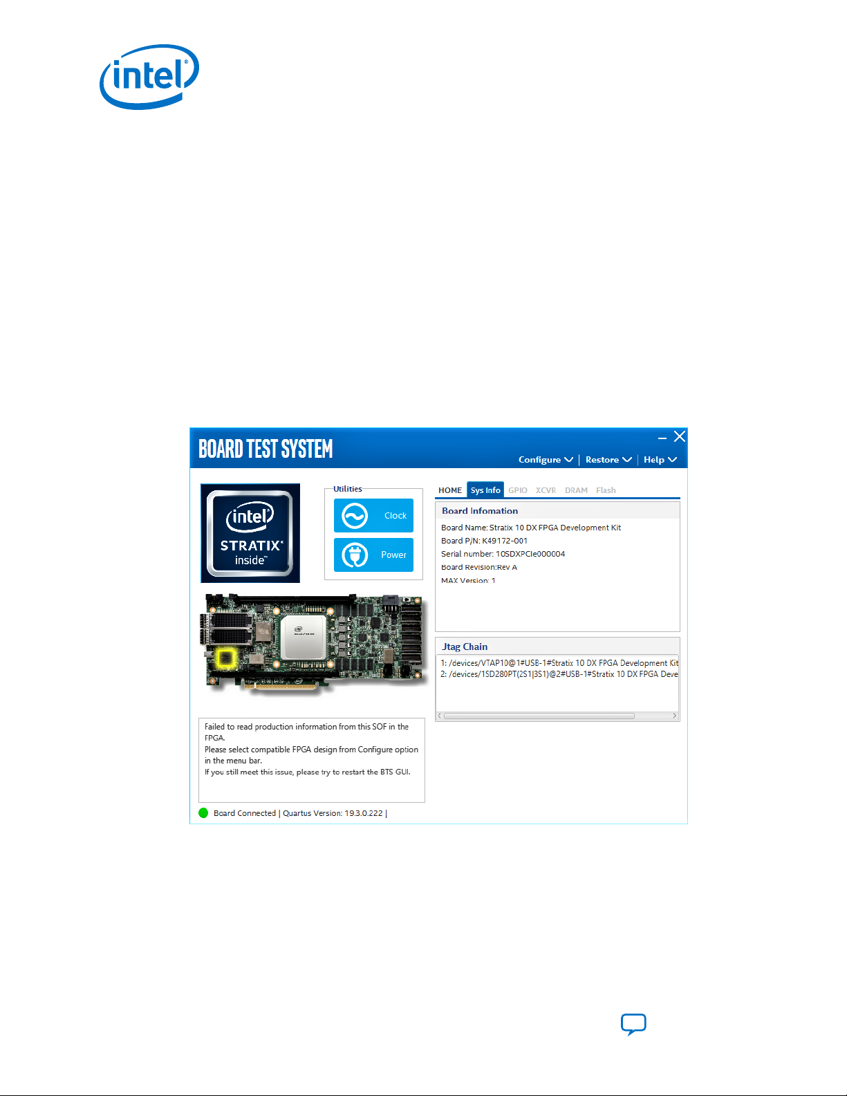
4.3.2. Sys Info Tab
The Sys Info tab shows the board's current configuration. The tab displays the
contents of the Intel MAX 10 registers, the JTAG chain, the Ethernet port numbers,
and other details stored on the board.
Figure 8. Sys Info Tab
The following sections describe the controls of the Sys Info tab.
Board Information
Displays static information about your board:
Intel® Stratix® 10 DX FPGA Development Kit User Guide
18
Send Feedback
Page 19
4. Board Test System (BTS)
UG-20255 | 2020.11.16
• Board Name: Indicates the official name of the board given by the BTS.
• Board P/N: Indicates the part number of the board.
• Serial Number: Indicates the serial number of the board.
• Board Revision: Indicates the revision of the board.
• MAX Version: Indicates the version of Intel MAX 10 code currently running on
the board.
JTAG Chain
Shows devices which are currently in the JTAG chain.
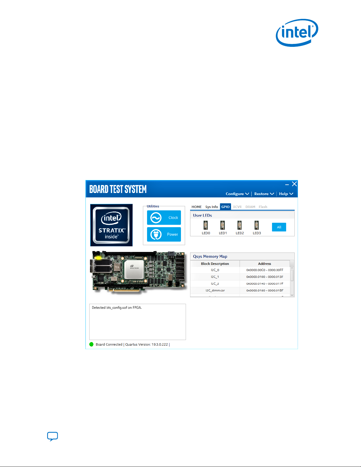
4.3.3. GPIO Tab
The GPIO tab allows you to interact with all the genral purpose user I/O components
on your board. You can turn LEDs on or off.
Figure 9. GPIO Tab
The following sections describe the controls on the GPIO tab:
User LEDs
Displays the current state of user LEDs. Toggle the LED buttons to turn the board LEDs
on and off.
Send Feedback
Intel® Stratix® 10 DX FPGA Development Kit User Guide
19
Page 20
Qsys Memory Map
Shows the memory map of the GPIO or FLASH Platform Designer system on your
board.
4.3.4. QSFP Tab
This tab allows you to perform loopback tests on the QSFP ports.
Figure 10. QSFP Tab
4. Board Test System (BTS)
UG-20255 | 2020.11.16
The following sections describe the controls on the QSFP tab:
Status
Displays the following status information during a loopback test:
Intel® Stratix® 10 DX FPGA Development Kit User Guide
20
Send Feedback
Page 21
4. Board Test System (BTS)
UG-20255 | 2020.11.16
• PLL Lock: Shows the PLL locked or unlocked state.
• Pattern sync: Shows the pattern synced or not synced state. The pattern is
considered synced when the start of the data sequence is detected.
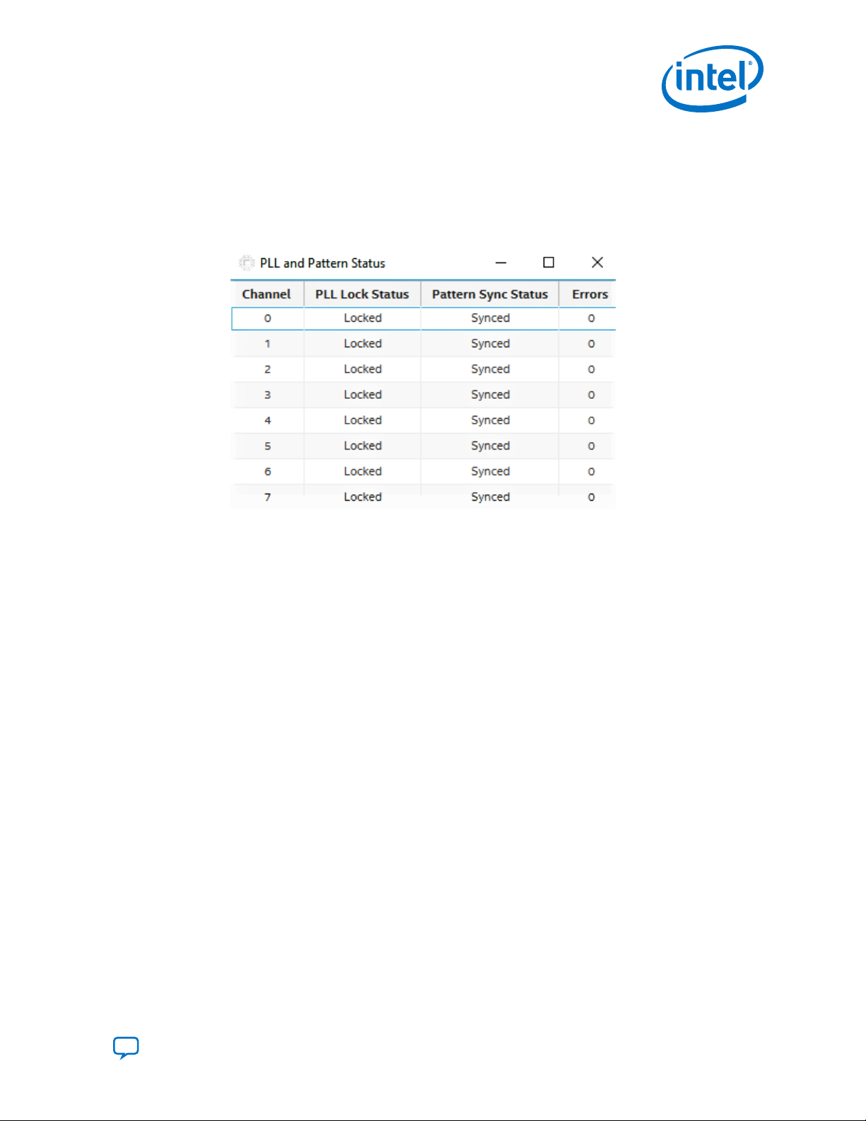
• Details: Shows the PLL lock and pattern sync status:
Figure 11. PLL and Pattern Status
Port
Allows you to specify which interface to test. The following port tests are available:
• QSFP x8
PMA Setting
Allows you to make changes to the PMA parameters that affect the active transceiver
interface. The following settings are available for analysis:
• Serial Loopback: Routes signals between the transmitter and the receiver.
• VOD: Specifies the voltage output differential of the transmitter buffer.
• Pre-emphasis tap:
— Pre-tap 1: Specifies the amount of pre-emphasis on the first pre-tap of the
transmitter buffer.
— Pre-tap 2: Specifies the amount of pre-emphasis on the second pre-tap of
the transmitter buffer.
— Pre-tap 3: Specifies the amount of pre-emphasis on the third pre-tap of the
transmitter buffer.
— Post-tap 1: Specifies the amount of pre-emphasis on the post-tap of the
transmitter buffer.
• Equalizer: Specifies the RX tuning mode for receiver equalizer.
Send Feedback
Intel® Stratix® 10 DX FPGA Development Kit User Guide
21
Page 22
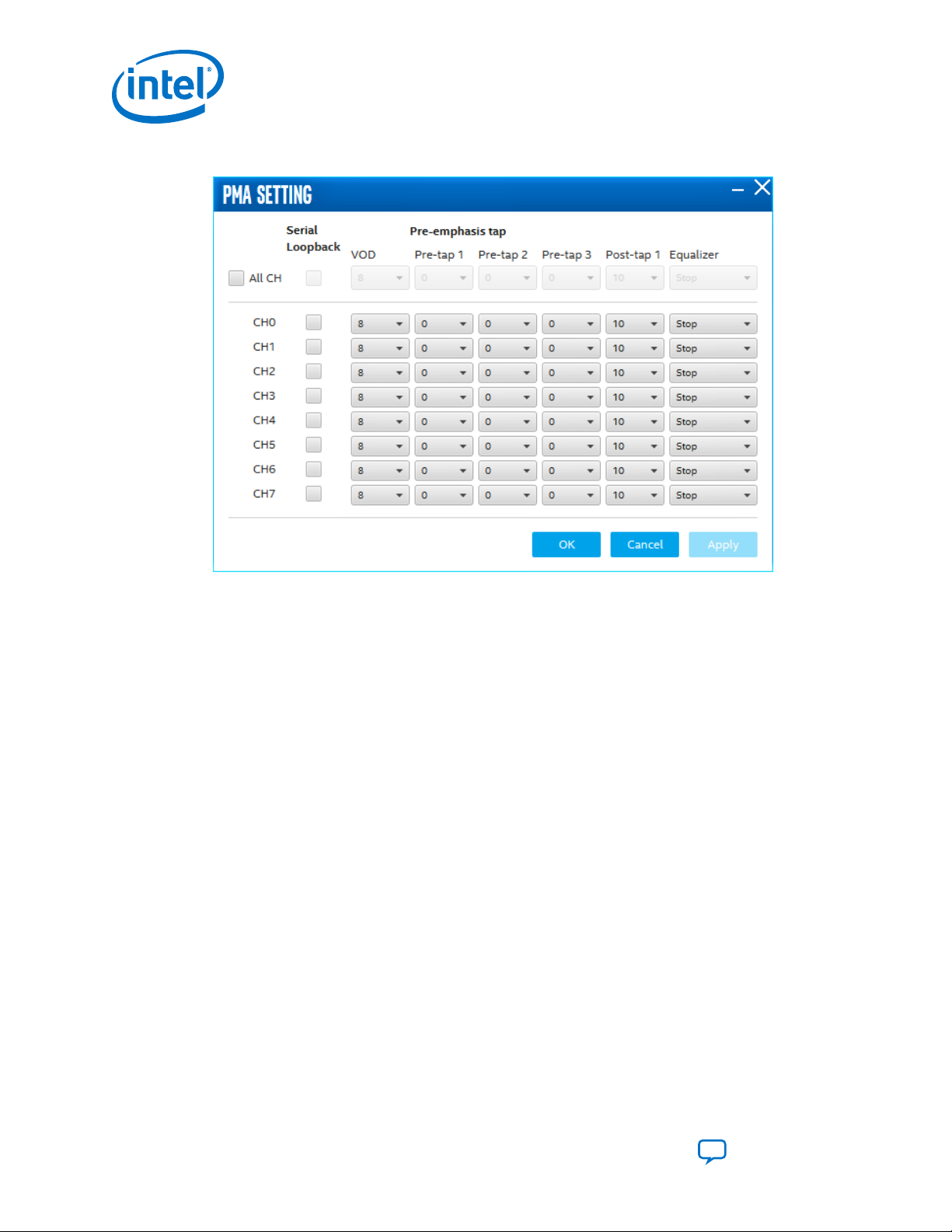
Figure 12. PMA Setting
4. Board Test System (BTS)
UG-20255 | 2020.11.16
Data Type
Specifies the type of data contained in the transactions. The following data types are
available for analysis:
• PRBS 7: Selects pseudo-random 7-bit sequences.
• PRBS 15: Selects pseudo-random 15-bit sequences.
• PRBS 23: Selects pseudo-random 23-bit sequences.
• PRBS 31: Selects pseudo-random 31-bit sequences.
• HF: Selects highest frequency divide-by-2 data pattern 10101010.
• LF: Selects lowest frequency divide-by-33 data pattern.
Error Control
Displays data errors detected during analysis and allows you to insert errors:
• Detected errors: Displays the number of data errors detected in the hardware.
• Inserted errors: Displays the number of errors inserted into the transmit data
stream.
• Insert: Inserts a one-word error into the transmit data stream each time you click
the button. Insert is only enabled during transaction performance analysis.
• Clear: Resets the detected errors and inserted errors counters to zero.
Intel® Stratix® 10 DX FPGA Development Kit User Guide
22
Send Feedback
Page 23

4. Board Test System (BTS)
UG-20255 | 2020.11.16
Loopback
• Start: Initiates the selected ports transaction performance analysis. Always click
Clear before Start.
• Stop: Terminates transaction performance analysis.
• TX and RX performance bars: Show the percentage of maximum theoretical
data rate that the requested transactions are able to achieve.
4.3.5. Component DDR4 CH0 Tab
This tab allows you to read and write Component DDR4 CH0 memory on your board.
Figure 13. Component DDR4 CH0 Tab
The following sections describe the controls on the Component DDR4 CH0 tab:
Start
Initiates DDR4 memory transaction performance analysis.
Stop
Terminates transaction performance analysis.
Performance Indicator
These controls display current transaction performance analysis information collected
since you last clicked Start:
Send Feedback
Intel® Stratix® 10 DX FPGA Development Kit User Guide
23
Page 24

4. Board Test System (BTS)
UG-20255 | 2020.11.16
• Write, Read and Total performance bars: Shows the percentage of maximum
theoretical data rate that the requested transactions are able to achieve.
• Write (MBps), Read (MBps) and Total (MBps): Shows the number of bytes
analyzed per second.
• Data Bus: 72-bits (8-bits ECC) wide and the frequency is 1066 MHz double data
rate. 2133 Mbps per pin. Equating to a theoretical maximum banwidth of 136,512
Mbps or 17,064 MBps.
Error Control
This control displays data errors detected during analysis and allows you to insert
errors:
• Detected errors: Displays the number of data errors detected in the hardware.
• Inserted errors: Displays the number of errors inserted into the transaction
stream.
• Insert: Inserts a one-word error into the transaction stream each time you click
the button. Insert error is only enabled during transaction performance analysis.
• Clear: Resets the detected error and inserted error counters to zero.
Address Range
Determines the number of addresses to use in each iteration of reads and writes.
4.3.6. Component DDR4 CH1 Tab
This tab allows you to read and write Component DDR4 CH1 memory on your board.
Intel® Stratix® 10 DX FPGA Development Kit User Guide
24
Send Feedback
Page 25

4. Board Test System (BTS)
UG-20255 | 2020.11.16
Figure 14. Component DDR4 CH1 Tab
The following sections describe the controls on the Component DDR4 CH1 tab.
Start
Initiates DDR4 memory transaction performance analysis.
Stop
Terminates transaction performance analysis.
Performance Indicators
These controls display current transaction performance analysis information collected
since you last clicked Start:
• Write, Read and Total performance bars: Shows the percentage of maximum
theoretical data rate that the requested transactions are able to achieve.
• Write (MBps), Read (MBps) and Total (MBps): Shows the number of bytes
analyzed per second.
• Data Bus: 72-bits (8-bits ECC) wide and the frequency is 1066 MHz double data
rate. 2133 Mbps per pin. Equating to a theoretical maximum banwidth of 136,512
Mbps or 17,064 MBps.
Error Control
This control displays data errors detected during analysis and allows you to insert
errors:
Send Feedback
Intel® Stratix® 10 DX FPGA Development Kit User Guide
25
Page 26

• Detected errors: Displays the number of data errors detected in the hardware.
• Inserted errors: Displays the number of errors inserted into the transaction
stream.
• Insert: Inserts a one-word error into the transaction stream each time you click
the button. Insert error is only enabled during transaction performance analysis.
• Clear: Resets the detected error and inserted error counters to zero.
Address Range
Determines the number of addresses to use in each iteration of reads and writes.
4.3.7. DDR4 DIMM CH0 Tab
This tab allows you to read and write Dual Inline Memory Module (DIMM) DDR4 CH0
memory on your board.
Figure 15. DDR4 DIMM CH0 Tab
4. Board Test System (BTS)
UG-20255 | 2020.11.16
The following sections describe the controls on the DDR4 DIMM CH0 tab:
Start
Initiates DDR4 memory transaction performance analysis.
Stop
Terminates transaction performance analysis.
Intel® Stratix® 10 DX FPGA Development Kit User Guide
26
Send Feedback
Page 27

4. Board Test System (BTS)
UG-20255 | 2020.11.16
Performance Indicators
These controls display current transaction performance analysis information collected
since you last clicked Start:
• Write, Read and Total performance bars: Shows the percentage of maximum
theoretical data rate that the requested transactions are able to achieve.
• Write (MBps), Read (MBps) and Total (MBps): Shows the number of bytes
analyzed per second.
• Data Bus: 72-bits (8-bits ECC) wide and the frequency is 1066 MHz double data
rate. 2133 Mbps per pin. Equating to a theoretical maximum banwidth of 136,512
Mbps or 17,064 MBps.
Error Control
This control displays data errors detected during analysis and allows you to insert
errors:
• Detected errors: Displays the number of data errors detected in the hardware.
• Inserted errors: Displays the number of errors inserted into the transaction
stream.
• Insert: Inserts a one-word error into the transaction stream each time you click
the button. Insert error is only enabled during transaction performance analysis.
• Clear: Resets the detected error and inserted error counters to zero.
Address Range
Determines the number of addresses to use in each iteration of reads and writes.
4.3.8. DDR4 DIMM CH1 Tab
This tab allows you to read and write Dual Inline Memory Module (DIMM) DDR4 CH1
memory on your board.
Send Feedback
Intel® Stratix® 10 DX FPGA Development Kit User Guide
27
Page 28

Figure 16. DDR4 DIMM CH1 Tab
4. Board Test System (BTS)
UG-20255 | 2020.11.16
The following sections describe the controls on the DDR4 DIMM CH1 tab:
Start
Initiates DDR4 memory transaction performance analysis.
Stop
Terminates transaction performance analysis.
Performance Indicators
These controls display current transaction performance analysis information collected
since you last clicked Start:
• Write, Read and Total performance bars: Shows the percentage of maximum
theoretical data rate that the requested transactions are able to achieve.
• Write (MBps), Read (MBps) and Total (MBps): Shows the number of bytes
analyzed per second.
• Data Bus: 72-bits (8-bits ECC) wide and the frequency is 1066 MHz double data
rate. 2133 Mbps per pin. Equating to a theoretical maximum banwidth of 136,512
Mbps or 17,064 MBps.
Error Control
This control displays data errors detected during analysis and allows you to insert
errors:
Intel® Stratix® 10 DX FPGA Development Kit User Guide
28
Send Feedback
Page 29

4. Board Test System (BTS)
UG-20255 | 2020.11.16
• Detected errors: Displays the number of data errors detected in the hardware.
• Inserted errors: Displays the number of errors inserted into the transaction
stream.
• Insert: Inserts a one-word error into the transaction stream each time you click
the button. Insert error is only enabled during transaction performance analysis.
• Clear: Resets the detected error and inserted error counters to zero.
Address Range
Determines the number of addresses to use in each iteration of reads and writes.
4.3.9. Power Monitor
The Power Monitor measures and reports current power information and
communicates with the Intel MAX 10 device on the board through the JTAG bus. A
power monitor circuit attached to the Intel MAX 10 device allows you to measure the
power that the Intel Stratix 10 DX FPGA is consuming.
To start the application, click the Power Monitor icon in the BTS. You can also run
the Power Monitor as a stand-alone application. The PowerMonitor.exe resides in
the <package dir>\examples\board_test_system directory.
Note: You cannot run the stand-alone power application and the BTS simultaneously. Also,
you cannot run power and clock interface at the same time.
Figure 17. Power Monitor Interface
Send Feedback
Intel® Stratix® 10 DX FPGA Development Kit User Guide
29
Page 30

4.3.10. Clock Controller
The Clock Controller application sets the Si5391 programmable oscillators to any
frequency between 0.16 MHz and 710 MHz.
The Clock Controller application sets the Si5332 programmable oscillators to any
frequency between 0.1 MHz and 712.5 MHz.
The Clock Control communicates with the Intel MAX 10 on the board through the JTAG
bus. The programmable oscillator are connected to the Intel MAX 10 device through a
2-wire serial bus.
Figure 18. Clock Controller - Si5391
4. Board Test System (BTS)
UG-20255 | 2020.11.16
Intel® Stratix® 10 DX FPGA Development Kit User Guide
30
Send Feedback
Page 31

4. Board Test System (BTS)
UG-20255 | 2020.11.16
Figure 19. Clock Controller - Si5332
Si5391 tab and Si5332 tab display the same GUI controls for each clock generators.
Each tab allows for separate control. The Si5391 is capable of synthesizing four
independent user-programmable clock frequencies up to 710 MHz.
The controls of the clock controller are described below:
F_vco
Displays the generating signal value of the voltage-controlled oscillator.
Register
Display the current frequencies for each oscillator.
Frequency
Allows you to specify the frequency of the clock in MHz.
Read
Reads the current frequency setting for the oscillator associated with the active tab.
Send Feedback
Intel® Stratix® 10 DX FPGA Development Kit User Guide
31
Page 32

Default
Sets the frequency for the oscillator associated with the active tab back to its default
value. This can also be accomplished by power cycling the board.
Set
Sets the programmable oscillator frequency for the selected clock to the value in the
CLK0 to CLK3 controls for the Si5391. Frequency changes might take several
milliseconds to take effect. You might see glitches on the clock during this time. Intel
recommends resetting the FPGA logic after changing frequencies.
Import
Import register map file generated from Silicon Laboratories ClockBuilder Desktop.
4.4. Smart VID Setting
If you are creating your own design and want to generate programming .sof file, you
must add the correct Smart VID Setting into Intel Quartus Prime project for Intel
Stratix 10 DX FPGA Development Kit to make configuration successfully. Before you
add the following Smart VID setting into the .qsf file, you must change the
configuration scheme to Avalon® streaming interface x8 for your project. You can also
extract the Smart VID setting from the Golden Top file.
4. Board Test System (BTS)
UG-20255 | 2020.11.16
For Intel Stratix 10 DX FPGA Development Kit (Production):
set_global_assignment -name USE_CONF_DONE SDM_IO16
set_global_assignment -name USE_CVP_CONFDONE SDM_IO5
set_global_assignment -name VID_OPERATION_MODE "PMBUS MASTER"
set_global_assignment -name USE_PWRMGT_SCL SDM_IO0
set_global_assignment -name USE_PWRMGT_SDA SDM_IO12
set_global_assignment -name PWRMGT_BUS_SPEED_MODE "100 KHZ"
set_global_assignment -name PWRMGT_SLAVE_DEVICE_TYPE ED8401
set_global_assignment -name PWRMGT_SLAVE_DEVICE0_ADDRESS 49
set_global_assignment -name PWRMGT_SLAVE_DEVICE1_ADDRESS 00
set_global_assignment -name PWRMGT_SLAVE_DEVICE2_ADDRESS 00
set_global_assignment -name PWRMGT_SLAVE_DEVICE3_ADDRESS 00
set_global_assignment -name PWRMGT_SLAVE_DEVICE4_ADDRESS 00
set_global_assignment -name PWRMGT_SLAVE_DEVICE5_ADDRESS 00
set_global_assignment -name PWRMGT_SLAVE_DEVICE6_ADDRESS 00
set_global_assignment -name PWRMGT_SLAVE_DEVICE7_ADDRESS 00
set_global_assignment -name PWRMGT_VOLTAGE_OUTPUT_FORMAT "LINEAR FORMAT"
set_global_assignment -name PWRMGT_LINEAR_FORMAT_N "-13"
set_global_assignment -name PWRMGT_TRANSLATED_VOLTAGE_VALUE_UNIT VOLTS
set_global_assignment -name PWRMGT_PAGE_COMMAND_ENABLE OFF
For Intel Stratix 10 DX FPGA Development Kit (ES1):
set_global_assignment -name USE_CONF_DONE SDM_IO16
set_global_assignment -name USE_CVP_CONFDONE SDM_IO5
set_global_assignment -name VID_OPERATION_MODE "PMBUS MASTER"
set_global_assignment -name USE_PWRMGT_SCL SDM_IO0
set_global_assignment -name USE_PWRMGT_SDA SDM_IO12
set_global_assignment -name PWRMGT_BUS_SPEED_MODE "100 KHZ"
set_global_assignment -name PWRMGT_SLAVE_DEVICE_TYPE OTHER
set_global_assignment -name PWRMGT_SLAVE_DEVICE0_ADDRESS 60
set_global_assignment -name PWRMGT_SLAVE_DEVICE1_ADDRESS 00
set_global_assignment -name PWRMGT_SLAVE_DEVICE2_ADDRESS 00
set_global_assignment -name PWRMGT_SLAVE_DEVICE3_ADDRESS 00
set_global_assignment -name PWRMGT_SLAVE_DEVICE4_ADDRESS 00
set_global_assignment -name PWRMGT_SLAVE_DEVICE5_ADDRESS 00
set_global_assignment -name PWRMGT_SLAVE_DEVICE6_ADDRESS 00
Intel® Stratix® 10 DX FPGA Development Kit User Guide
32
Send Feedback
Page 33

4. Board Test System (BTS)
UG-20255 | 2020.11.16
set_global_assignment -name PWRMGT_SLAVE_DEVICE7_ADDRESS 00
set_global_assignment -name PWRMGT_VOLTAGE_OUTPUT_FORMAT "DIRECT FORMAT"
set_global_assignment -name PWRMGT_DIRECT_FORMAT_COEFFICIENT_M 1
set_global_assignment -name PWRMGT_DIRECT_FORMAT_COEFFICIENT_R 3
set_global_assignment -name PWRMGT_TRANSLATED_VOLTAGE_VALUE_UNIT VOLTS
set_global_assignment -name PWRMGT_PAGE_COMMAND_ENABLE OFF
Send Feedback
Intel® Stratix® 10 DX FPGA Development Kit User Guide
33
Page 34

UG-20255 | 2020.11.16
Send Feedback
5. Development Kit Hardware and Configuration
5.1. FPGA Configuration
Prerequisites:
• Install the Intel Quartus Prime Pro Edition and Intel FPGA Download Cable II driver
on the host computer.
• Connect the micro-USB cable to the Intel Stratix 10 DX FPGA Development Kit.
• Power-on the board. Ensure that no running application is using the JTAG chain.
Follow these steps to configure the FPGA with your SRAM Object File (.sof) using the
Intel Quartus Prime Pro Edition Programmer:
1. Start the Intel Quartus Prime Pro Edition Programmer.
2. Click Auto Detect to display the devices in the JTAG chain.
3.
Click Change File and select the path to the desired *.sof file.
4. Turn on the Program or Configure option for the added file.
5. Click Start to download the selected file to the FPGA. The configuration is
completed successfully when the progress bar reaches 100%.
Using the Intel Quartus Prime Pro Edition Programmer to configure a device on the
board causes other JTAG- based applications such as the Board Test System and the
Power Monitor to lose their connection to the board. Restart those applications after
the configuration is complete.
Note: While using the Intel Quartus Prime Pro Edition software version 19.3, you may
observe occasional crash. Contact Intel support to access additional patch (0.01) for
Intel Quartus Prime Pro Edition Programmer to mitigate this issue.
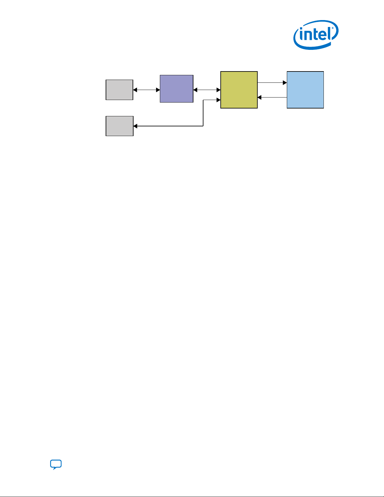
5.2. Programming the FPGA Over Intel FPGA Download Cable
The figure below shows the high-level conceptual block diagram for programming the
Intel Stratix 10 DX FPGA over the embedded Intel FPGA Download Cable or external
Intel FPGA Download Cable.
Intel Corporation. All rights reserved. Agilex, Altera, Arria, Cyclone, Enpirion, Intel, the Intel logo, MAX, Nios,
Quartus and Stratix words and logos are trademarks of Intel Corporation or its subsidiaries in the U.S. and/or
other countries. Intel warrants performance of its FPGA and semiconductor products to current specifications in
accordance with Intel's standard warranty, but reserves the right to make changes to any products and services
at any time without notice. Intel assumes no responsibility or liability arising out of the application or use of any
information, product, or service described herein except as expressly agreed to in writing by Intel. Intel
customers are advised to obtain the latest version of device specifications before relying on any published
information and before placing orders for products or services.
*Other names and brands may be claimed as the property of others.
ISO
9001:2015
Registered
Page 35
USB PHY Intel MAX 10
Intel Stratix 10
DX FPGA
USB
Connection
JTAG
Connection
USB Data
JTAG
5. Development Kit Hardware and Configuration
UG-20255 | 2020.11.16
Figure 20. Programming Concept Block Diagram
5.3. Configuration Modes
The Intel Stratix 10 DX FPGA Development Kit supports two configuration modes:
• Avalon Streaming Interface x8 - using the 2Gb QSPI Flash device (U66)
• JTAG - using either the embedded Intel FPGA Download Cable or external Intel
FPGA Download Cable.
5.3.1. Avalon Streaming Interface x8 Mode
The SDM block in the Intel Stratix 10 DX FPGA device controls the configuration
process and interface. The Intel MAX 10 System Controller (U11) interfaces to Intel
Stratix 10 DX FPGA in Avalon Streaming Interface X8 mode.
For Avalon Streaming Interface x8 mode, the MSEL[2:0] configuration pin strapping
(SW1) must be set to [110] (which means SW1.1: ON (Close), SW1.2: OFF (Open),
SW1.3: OFF (Open)).
5.3.1.1. Avalon Streaming Interface x8 Configuration Guideline
Ensure the following conditions are met before you proceed:
• The Intel Quartus Prime Programmer and the Intel FPGA Download Cable II driver
are installed on the host computer.
• If you are using an external JTAG programmer, ensure the Intel FPGA Download
Cable II is connected to the board through the 10-pin female connector. Verfiy
that the Intel FPGA Download Cable II LED for proper connection to the host
computer through a micro-USB cable.
• Power to the board is on, and no other applications that use the JTAG chain are
running.
Avalon Streaming Interface x8 Programmer Object File (.pof) Generation using the Intel Quartus Prime Pro Edition software version 20.1 or later
Note:
If you already have the Programmer Object File (.pof), you can skip this
section.
1. Open the Intel Quartus Prime Pro Edition software and click on File >
Programming File Generator to launch Programming File Generator tool.
2. In the Device Family list, select Stratix 10, and in the Configuration mode
list, select AVST x8 to specify the device and configuration mode.
Send Feedback
Intel® Stratix® 10 DX FPGA Development Kit User Guide
35
Page 36

3. In the Output directory tab, click Browse to specify the output directory
for .pof file, in the Name column, input filename for .pof file.
4. In the Description column, select the Programmer Object File (.pof) and
Memory Map File (.map) option.
Figure 21. Step 2 to 4 Illustration
5. Development Kit Hardware and Configuration
UG-20255 | 2020.11.16
5.
Click on Input Files>Add Bitstream tab to specify a .sof that contains the
configuration bitstream.
Figure 22. Step 5 Illustration
6. Click on Configuration Device>Add Device to specify the flash device. In the
Device list of the pop-up window, select CFI_2Gb for the configuration flash
device.
Intel® Stratix® 10 DX FPGA Development Kit User Guide
36
Send Feedback
Page 37

5. Development Kit Hardware and Configuration
UG-20255 | 2020.11.16
7. Click on OPTIONS row, and then click on Edit option to modify the start address.
In the Address Mode list of the pop-up window, select Start; in the Start
address list, input 0x00010000.
Figure 23. Step 7 Illustration
8. Click on CFI_2Gb row, and then click Add Partition option. In the Input file list
of pop-up window, select Bitstream (input_sof_file.sof); in the Address Mode
list of pop-up window, select Start; in the Start address list, input
0x00100000.
Figure 24. Step 8 Illustration
9.
Click Generate to generate the .pof file.
Send Feedback
Intel® Stratix® 10 DX FPGA Development Kit User Guide
37
Page 38

5. Development Kit Hardware and Configuration
UG-20255 | 2020.11.16
Avalon Streaming Interface x8 Programmer Object File (.pof) Generation using the Intel Quartus Prime Pro Edition software version 19.3 or 19.4
The avstx8.cof and avstx8.cdf are included in the factory_recovery folder of
installer package.
Note: If you already have the Programmer Object File (.pof), you can skip this section.
1.
Open avstx8.cof using the text editor.
2.
Change the .pof file name and directory based on your local output file name and
directory, the location is marked as 1 in the figure below.
3.
Change the .sof file name and directory based on your local input file name and
directory, the location is marked as 2 in the figure below.
Figure 25. Step 2 and 3 Illustration
4.
Save the change and close the avstx8.cof file.
5. Open the Intel Quartus Prime Pro Edition software 19.3 or later version, and click
on File > Convert Programming Files to launch Convert Programming File
tool.
6.
Click on Open Conversion Setup Data to locate the recently saved avstx8.cof
file and open it.
Intel® Stratix® 10 DX FPGA Development Kit User Guide
38
Send Feedback
Page 39

5. Development Kit Hardware and Configuration
UG-20255 | 2020.11.16
Figure 26. Step 6 Illustration
7.
Click Generate to generate the .pof file.
QSPI Flash Programming with Avalon Streaming Interface x8 Configuration Testing
1.
Open avstx8.cdf using the text editor.
2.
Change the .pof file name and directory based on your local output file name and
directory, the location is marked as 1 in the figure below. Ensure to save the file.
Figure 27. Step 2 Illustration
3. Change switch SW33.1 to OFF (1'b0:far from board edge) position for normal
JTAG mode.
4. Plug in the USB dongle to external JTAG header (J2) or plug in the USB cable into
micro USB port (CN1).
5. Plug ATX Power into J42, switch SW31 to turn ON the Intel Stratix 10 FPGA
power.
6. Open the Intel Quartus Prime Pro Edition software 19.3 or later version, and open
avstx8.cdf file.
Send Feedback
Intel® Stratix® 10 DX FPGA Development Kit User Guide
39
Page 40

Figure 28. Step 6 Illustration
7. Click on Hardware Setup in the Intel Quartus Prime Programmer to change
Hardware frequency to 16 MHz.
Use the following command to change TCK frequency to 16 MHz:
jtagconfig --setparam <cable_number> JtagClock 16M
8. Click on Start to start QSPI Flash programming.
9. After programming is successful, change switch SW31 to power OFF, and unplug
the ATX power from J42 to completely power down the development kit. Change
the MSEL(SW1) to 110 (AVSTx8, SW1.1: ON (Close), SW1.2: OFF (Open),
SW1.3: OFF (Open))
Note: If the development kit is installed in the server, you must power off the
server and power it on to completely power cycle the development kit.
10. Plug ATX Power into J42 and change switch SW31 to power ON the development
kit. Observe whether the D57 is ON (ON means the AVST x8 configuration is
successful).
5. Development Kit Hardware and Configuration
UG-20255 | 2020.11.16
5.3.2. JTAG Mode
The JTAG Switch implemented in the Intel MAX 10 System Control (U11) allows the
selection of the device(s) to be included in the JTAG chain. It is done by the settings of
the DIP switch SW33. The embedded Intel FPGA Download Cable (or external Intel
FPGA Download Cable) or PCIe JTAG can be selected as the source for programming
the device(s) on the chain. The embedded Intel FPGA Download Cable is the default
setting for this configuration mode.
Intel® Stratix® 10 DX FPGA Development Kit User Guide
40
Send Feedback
Page 41

MT25QLO2G
2Gb
QSPI FLASH
U66
W25Q64
8MB
NIOS FLASH
U41
GPIOsGPIOs
DCII
USB_MAX_ JTAG
EXT_UBII_ JTAG
Micro-USB
Conn
CN1
USB
PD[3:0]
U49
Data/Ctrl
QSPI_M10_DATA 0-3
USB_MAX_JTAGSEL
SW33_1
USB_DISABLEn
BMC_JTAG
3.3V 1.8V
JTAG_INPUT SOURCE
1.8V
1.8V
SPI_D0-3
Configuration 1.8V
1.8V
S10_1V8_JTAG
SW33_2
PCIE_PRSNT x1,x4, x8, x16 /
WAKEn /CLKREQn
0:PCIe BMC
1: ON-Board DCII
(Default)
USB_MAX_JTAGSEL
0:Normal Mode (Default)
1: External Intel FPGA
Download Cable II (DCII)
GPIOs
GPIOs
MAX 10
U11
USB PHY
CY7C6801
U26
EXT. JTAG
10-Pin Hrd
J2
nCONFIG
nSTATUS
INIT_DONE
CONFIG_DONE
JTAG
Intel Stratix 10 DX
Bank 2J
PCIE EDGE CONNECTOR J9
MAX3378
Level Shifter
U204, U212
Schmit Trig
Buffers
U64, U68
JTAG
CONTROL
5. Development Kit Hardware and Configuration
UG-20255 | 2020.11.16
Figure 29. JTAG Chain
The on-board Intel FPGA Download Cable is implemented in a Intel MAX 10 device. A
micro-USB connector connecting to a CY7C68013A USB2 PHY provides the data to
Intel MAX 10 device. This allows you to configure the FPGA using a USB cable, which
is directly connected to a host PC running Intel Quartus Prime Pro Edition software
without requiring the external Intel FPGA Download Cable.
You can also use the external Intel FPGA Download Cable on J2 to configure the FPGA.
Send Feedback
Intel® Stratix® 10 DX FPGA Development Kit User Guide
41
Page 42

UG-20255 | 2020.11.16
Send Feedback
6. Document Revision History for Intel Stratix 10 DX FPGA Development Kit User Guide
Document
Version
2020.11.16 Clarified the Smart VID Setting for ES1 and Production version of the Intel Stratix 10 DX FPGA
Development Kit.
2020.11.04 Sections updated:
• About this Document on page 4
• Default Switch Settings on page 9
• Connectors and LEDs on page 12
• Smart VID Setting on page 32
• Development Kit Components on page 43
• Components Overview on page 44
• Power Distribution on page 49
• Power Measurement on page 52
• I2C Interface on page 66
2020.08.17 Clarified the default position for Switch Settings.
2020.04.20 Updated steps in section: Avalon Streaming Interface x8 Programmer Object File (.pof) Generation.
2019.12.09 Initial release.
Changes
Intel Corporation. All rights reserved. Agilex, Altera, Arria, Cyclone, Enpirion, Intel, the Intel logo, MAX, Nios,
Quartus and Stratix words and logos are trademarks of Intel Corporation or its subsidiaries in the U.S. and/or
other countries. Intel warrants performance of its FPGA and semiconductor products to current specifications in
accordance with Intel's standard warranty, but reserves the right to make changes to any products and services
at any time without notice. Intel assumes no responsibility or liability arising out of the application or use of any
information, product, or service described herein except as expressly agreed to in writing by Intel. Intel
customers are advised to obtain the latest version of device specifications before relying on any published
information and before placing orders for products or services.
*Other names and brands may be claimed as the property of others.
ISO
9001:2015
Registered
Page 43

UG-20255 | 2020.11.16
Send Feedback
A. Development Kit Components
This appendix provides detailed information about the Intel Stratix 10 DX FPGA
Development Kit components.
Figure 30. Development Kit Front
Figure 31. Development Kit Back
Intel Corporation. All rights reserved. Agilex, Altera, Arria, Cyclone, Enpirion, Intel, the Intel logo, MAX, Nios,
Quartus and Stratix words and logos are trademarks of Intel Corporation or its subsidiaries in the U.S. and/or
other countries. Intel warrants performance of its FPGA and semiconductor products to current specifications in
accordance with Intel's standard warranty, but reserves the right to make changes to any products and services
at any time without notice. Intel assumes no responsibility or liability arising out of the application or use of any
information, product, or service described herein except as expressly agreed to in writing by Intel. Intel
customers are advised to obtain the latest version of device specifications before relying on any published
information and before placing orders for products or services.
*Other names and brands may be claimed as the property of others.
ISO
9001:2015
Registered
Page 44

A. Development Kit Components
A.1. Components Overview
Table 8. Intel Stratix 10 DX FPGA Development Kit Components
Board Reference Component Description
Featured Devices
• Logic elements: 2.8M
• DSP blocks: 5760
• M20K memory blocks: 11721
U1 Intel Stratix 10 DX FPGA
U11 Intel MAX 10
X4 Intel MAX 10 Reference Clock
U7
U9
J9 PCIe x16 gold fingers PCIe TX/RX x16 interface from FPGA P-tile 10A
J38 PCIe x16 or UPI x20, Link 1 PCIe/UPI Transmit interface from FPGA P-tile 11B
J40 PCIe x16 or UPI x20, Link 1 PCIe/UPI Receive interface from FPGA P-tile 11B
J39 PCIe x16 or UPI x20, Link 2 PCIe/UPI Transmit interface from FPGA P-tile 11C
Programmable Clock Generator
Si5332A
Programmable Clock Generator
Si5391A
Transceiver Interfaces
• Package type: 2912 BGA
• Transceiver count: 84
— 4x P-Tile supporting PCIe X16 Gen4 (16 Gb/s) or UPI X
20 (1up to 11.2 GT/s)
— 1x E-Tile transceiver supporting 2x 56Gbps PAM4 or 4x
25Gbps NRZ
• Logic elements: 50K
• Package type: 256 FBGA
•
1.8V VCCINT
Clock Circuits
The crystal oscillator provides the reference clock for Intel
MAX 10 device:
•
Out= 125.00 MHz
Default frequencies:
•
Out0 = 100.00 MHz
•
Out1 = 125.00 MHz
•
Out2 = 133.333MHz
•
Out3 = 133.333MHz
•
Out4 = 133.333 MHz
•
Out5 = 133.333MHz
•
Out6 = 100.00 MHz
•
Out7 = 100.00MHz
Default frequencies:
•
CLK0 = 156.25MHz
•
CLK0A = 156.25 MHz
•
CLK1 = 312.50 MHz
•
CLK2 = 312.50 MHz
•
CLK3 = 312.50 MHz
•
CLK4 = Not used
•
CLK5 = Not used
•
CLK6 = 100.00 MHz
•
CLK7 = 100.00 MHz
•
CLK8 = 100.00 MHz
•
CLK9 = 100.00 MHz
•
CLK9A = 100.00 MHz
UG-20255 | 2020.11.16
continued...
Intel® Stratix® 10 DX FPGA Development Kit User Guide
44
Send Feedback
Page 45

A. Development Kit Components
UG-20255 | 2020.11.16
Board Reference Component Description
J41 PCIe x16 or UPI x20, Link 2 PCIe/UPI Receive interface from FPGA P-tile 11C
J55 PCIe x16 or UPI x20, Link 0 PCIe/UPI Transmit interface from FPGA P-tile 10B
J65 PCIe x16 or UPI x20, Link 0 PCIe/UPI Receive interface from FPGA P-tile 10B
J15 QSFP 1 connector Four TX/RX channels from FPGA Bank 4F
J18 QSFP 2 connector Four TX/RX channels from FPGA Bank 4F
General User Input/Output
D9, D10, D14, D15 User defined LEDs Four green-color user LEDs. Illuminates when driven low
Memory
One X72 memory interface supporting DDR4 (x72) or Intel
Optane DC Persistent memory module:
J73 DDR4 x72 DIMM connector
J74 DDR4 x72 DIMM connector
U142, U143, U144,
U145, U146
U152, U153, U154,
U155, U156
U41 NIOS Flash 64K-bit This on-board Flash is for Intel MAX 10
U66 QSPI 2 Gbit NOR Flash This on-board Flash is for image storage for FPGA
J9 PCI Express x16 edge connector
J15 QSFP 1 Interface Provides four transceiver channels for a 100G QSFP module
J18 QSFP 2 Interface Provides four transceiver channels for a 100G QSFP module
J97 I2C/PMBus connector For accessing core power controller
J17 I2C connector For cccessing the I2C1 bus
J2 External JTAG Port
CN1 Micro-USB connector
J9 PCI Express edge connector
J42 DC input jack
On-board DDR4 x72 Memory
interface
On-board DDR4 x72 Memory
interface
Communication Ports
• DDR4 memory (x72) 1333 MHz
• Intel Optane DC Persistent memory (requires memory
controller IP core)
One X72 memory interface supporting DDR4 (x72) or Intel
Optane DC Persistent memory module:
• DDR4 memory (x72) 1333 MHz
• Intel Optane DC Persistent memory (requires memory
controller IP core)
This on-board DDR4 x72 memory supports 8 GB at up to 1200
MHz
This on-board DDR4 x72 memory supports 8 GB at up to 1200
MHz
Gold-plated edge fingers for up to x16 signaling in either
Gen1, Gen2, Gen3, or Gen4 mode
This port allows the use of Intel FPGA Download Cable II
dongle to access the JTAG links on the board. Connection to
this port automatically disables the internal Intel FPGA
Download Cable II JTAG.
Embedded Intel Intel FPGA Download Cable II JTAG for
programming the FPGA via USB cable.
Power Supply
Interfaces to a PCI Express root port such as an appropriate
PC motherboard for 12V power source
Accepts a 12 V DC power supply when powering the board
from the provided power brick for lab bench operation.
continued...
Send Feedback
Intel® Stratix® 10 DX FPGA Development Kit User Guide
45
Page 46

A. Development Kit Components
UG-20255 | 2020.11.16
Board Reference Component Description
When operating from the PCIe slot, this input must also be
connected to the 8-pin Aux PCIe power connector provided by
the PC system along with J42, or else the board will not power
on.
SW31 Power switch
U217 12V Hot Swap Controller Provide protection for AUX power input (J42)
U96 12V Hot Swap Controller Provide protection for PCIe slot power input (J9)
U93 Controlled power FET
U101 3.3V Voltage regulator Provides 3.3V to power system
U99 5V Voltage regulator Provides 5V to power system
U47,U240,U77,U24
1,U242
U230 0.9V Voltage regulator Provides power to all power rails in Group 1
U113 1.8V Voltage regulator Provides power to VCCPT and other rails in Group 2
U186 1.8V Voltage regulator Provides power to VCCH and VCCCLK for P-tiles
U184 1.1V Voltage regulator Provides power to VCCH for E-tile
U78 2.5V Voltage regulator Provides power to VCCCLK for E-tile
U76 2.4V Voltage regulator Provides power to VCCFUSEWR_SDM of Intel Stratix 10 FPGA
U188 1.8V Voltage regulator Provides power to VCCIO of Intel Stratix 10 FPGA
U116 1.2V and 2.5V Voltage regulator Provides power to Intel MAX 10 core and other rails
U79 1.8V Voltage regulator Provides power to VCCIO of Intel MAX 10
U163 2.5V Voltage regulator Provides power to DDR4 Channel 0
U164 0.6V Voltage regulator Provides power to DDR4 VTT Channel 0
U159 1.2V Voltage regulator Provides power to DDR4 Channel 0
U165 2.5V Voltage regulator Provides power to DDR4 Channel 1
U166 0.6V Voltage regulator Provides power to DDR4 VTT Channel 1
U157 1.2V Voltage regulator Provides power to DDR4 Channel 1
U192, U193 0.6V Precision voltage reference Provides reference voltage to DDR4 Channel 0 and Channel 1
U136 Controlled power FET Control power to all memory voltage regulators
U51 Power protector Provides power protection to QSFP 1 (J16)
U52 Power protector Provides power protection to QSFP 2 (J18)
4-phase VCC Core Voltage
regulator
Switch to power ON or OFF the board when supplied from the
DC input jack
Perform power bridging function between AUX2 and PCIe slot
when the board is not used in PCIe system
Provides power to VCC core of Intel Stratix 10 FPGA
Intel® Stratix® 10 DX FPGA Development Kit User Guide
46
Send Feedback
Page 47

A. Development Kit Components
UG-20255 | 2020.11.16
A.2. Power, Thermal, and Mechanical Considerations
A.2.1. Power Guidelines
This section describes the power supply for Intel Stratix 10 DX FPGA Development Kit.
A laptop-style DC power supply is provided with the development kit. Use only the
supplied power supply. The power supply has an auto-sensing input voltage of
100-240 V AC power and will output 12 V DC power at 20 A to the development
board. The 12 V DC input power is then stepped down to various power rails used by
the board components.
An on-board multi-channel analog-to-digital converter (ADC) measures both the
voltage and current for several specific board rails. The power utilization is displayed
on a graphical user interface (GUI) that can graph power consumption versus time.
The Intel Stratix 10 DX FPGA Development Kit has two modes of operation:
• Standard PCIe compliant system
In this mode, plug the board into an available PCI Express slot and connect the
standard 2x4 power cords available from the PC's ATX power supply to J11 on the
board. The PCIe slot together with the auxiliary PCIe power cords are required to
power the entire board. If you do not connect the 2x4 auxiliary power connection,
the board does not power on. The power switch SW3 is ignored when the board is
used in the PCIe system.
Figure 32. Setup Example
Send Feedback
Intel® Stratix® 10 DX FPGA Development Kit User Guide
47
Page 48

• Standalone evaluation board powered by included power supply
In this mode, plug the included power supply into the 2x4 pin connector (J42) and
the AC power cord of the power supply into a power outlet. This power supply
provides the entire power to the board without the need to obtain power from the
PCIe slot. The power switch SW31 controls powering of the board.
Figure 33. Setup Example
A. Development Kit Components
UG-20255 | 2020.11.16
Intel® Stratix® 10 DX FPGA Development Kit User Guide
48
Send Feedback
Page 49

J42
12V_AUX2
12V_AUX2_IN
12V@1.5A
12V
ATX 2x4
(150W)
12.5A
240W Power
Adapter 20A
12V_PCle_Slot
5VO
DDR4_CH11_EN
DDR4_CH00_EN
0V6_DDR4_VREF_CH00_EN
2.9A
0.2A
0v6_DDR4_VREF_CH11_EN
2.5V_DDR4_CH11_EN
2V5_DDR4_CH11
0.08A
EP53F8QI
2.5V@1.5A
U163
EV1320QI
0.6V@2A
U164
EN63A0
1.2V@12A
U159
3.3V_ZQSFP1
3.3V_ZQSFP2
3.3V@1.5A
3.3V@1.5A
HSC
MAX16550
U96
LTC4359
U93
VCCH_GXP_EN
0.87A
VC??_GXE_EN
0.8A
VCCCLK_GXE_EN
0.36A
VCCFUSE_EN
3.2A
VCCID_1V?EN
0.7A
ED8401 +
4X ET6160
4.5A
0.9V@54A
7.8A
0.85V@110A
93.5W
VCC_EN
IN
OUT
1.8V_IN
VCCFUSEWR_SDM
2.4V@0.5A
2.5V@1A
S10_VCCH_GXE
1.1V@2.62A
1.8V@1.3A
S10_G2_1.8V_FLT
0.17A
2.7A
4A
0.5A
0p9V
VCC, VCCP
7.6A
0.01A
0.01A
41.79A
0.17A
0.46A
2.45A
19.6A
12V@1.5A
1.8V@18A
VCCERAM_EN
S10_G2_1.8V
11.3A
3.3V
1A
5V
12V_DDRT_DIMM01
3.3V_REG_INST
3.3V_REG_INST
12V_PCIE_IN
LTC4357
Ideal Diode
Ctlr
U97
8.3A
518_VCCH_GXP_LOW
1.8V@0.5A
M10_3.3V
MAX10_VCCIO_2.5V
MAX10_VCCIO_1.2V
1.2V@1A
1.8V
6A
2.5V@0.2A
MAX10_VCCIO_1.8V
S10 (U1) S10_VCCPLL_SDM, S10_VCCADC, S10_VCCA_PLL
S10 (U1) S10_VCCPT, VCCBAT
S10 (U1) VCCCLK_GXP
S10 (U1) VCCH_GXP
S10 (U1) VCC, VCCP
S10 (U1) VCCRTPLL_GXE
S10 (U1) VCCRT_GXE
S10 (U1) VCCRAM
S10 (U1) S10_VCCPLLDIG_SDM
S10 (U1) S10_VCCFUSE_GXP
S10 (U1) VCCS10_VCCFUSE_GXP
S10_(U1) VCCPFUSEWR_SDM
1.8V
S10 (U1)
S10_VCCIO_SDM, S10_VCCBAT, S10_VCCOO_2I, S10_VCCOO_2J,
S10_VCCIO_2N, S10_VCCIO_3L, S10_VCCIO_3H
2v5_DDR4_CH11
0V6_DDR4_VTT_CH11
S10_IV2OUT_CH11
0V6_DDR4_VREF_CH11
12V_DORT_DIMM00
2.5V_DDR4_CH00_EN
2.5V@0.1A
2.5V@0.1A
3.3V_REG
3.3V_REG_EN
U136
10.2A
0.6V@1A
1.2V@8A
2V5_DDR4_CH00
0.6V@1A
1.2V@?A
U203
TPS2557 (U51)
QSFP1 (116)
QSFP2 (1??)
TPS2557 (U52)
FP53F8QI
1.8V@1.5A
U79
S10 (U1) VCCH_GXE
S10 (U1) VCCCLK_GXE
S10_VCCCLK_GXE_LOW 2.5V
Power on
Group 1
Power-up Sequence
Power-down Sequence
Monitored Power Rails
Group 2
Group 3
Group 3
Group 2
Group 1
VCC/VCCP
VCCPT (U113)
0.9V (U230)
3.3V (U101)
12V_AUX2
12V_PCIE_IN
.....
.....
.....
.....
.....
.....
.....
.....
.....
.....
.....
.....
.....
.....
.....
.....
.....
.....
LC
EP53F8QI
2.5V@1.5A
U78
EN6382QI
1.8V@8A
U188
EP53F8QI
2.4V@1.5A
U76
EZ6303QI
1.2V@2.2A
2.5V@0.3A
U116
EN6382
1.1V@8A
U184
EN63A0
1.8V@12A
U186
MAX10_VCC_1.2V
M10_VCCINT
M10_3.3V
MAX10_VCCID_1.8V
M10_1V2_VCCDPLL
MAX10_VCCA_2.5V
MAX10_VCCA_ADC_2.5V
.....
.....
LC
F
.....
.....
LC
EM2260
0.9V@60A
U230
EM2130H
3.3V@30A
U101
EM2130H
1.8V@30A
U113
NCP45560
EP53F8QI
2.5V@1.5A
U165
EV1320QI
0.6V@2A
U166
EN63A0
1.2V@12A
U157
HSC
MAX16550
U217
0V6_DDR4_VTT_CH00
S10_IV2OUT_CH00
2v5_DDR4_CH00
0V6_DDR4_VREF_CH00
ER2120QI
5.0V@2A
U99
SV0
12V
PCle Slot
(75W)
5.5A
A. Development Kit Components
UG-20255 | 2020.11.16
A.2.1.1. Power Distribution
The power distribution system on the Intel Stratix 10 DX FPGA Development Kit is
shown below.
Figure 34. Power Tree Diagram
Send Feedback
Intel® Stratix® 10 DX FPGA Development Kit User Guide
49
Page 50

A. Development Kit Components
Table 9. Power Supply List
Maximum
Source Name Power Name
ED8401(U47)
EN2260 (U230) 0.9V
EN2130H (U113) 1.8V
EN63A0 (U186) 1.8V
EN63A0 (U184) 1.1V S10_VCCH_GXE 8 Analog power for E-Tile
EP53F8QI (U78) 2.5V
EP53F8QI (U76) 2.4V S10_VCCFUSEWR_SDM 0.5 Fuse power for SDM
EN6382QII (U188) 1.8V S10_VCCIO 6
EZ6303QI (U116) 1.2V
EZ6303QI (U116) 2.5V M10_VCCA/VCC_ADC 0.2
FP53F8QI (U79) 1.8V M10_VCCIO 1
EM2130H(U101) 3.3V 3.3V_REG_INST 30 System 3.3V rail
EV1320QI (U164) 0.6V 0p6V_DDR4_VTT_CH00 0.02
EP53F8QI (U163) 2.5V 2V5_DDR4_CH00 0.1 2.5V rail for DDR4
EN63A0 (U159) 1.2V S10_1v2OUT_CH00 12 Memory IO power for Ch00
EV1320QI (U166) 0.6V 0p6V_DDR4_VTT_CH11 0.02
EP53F8QI (U165) 2.5V 2V5_DDR4_CH11 0.1 2.5V rail for DDR4
VCC
VCCP Periphery power
S10_VCCERAM
VCCPLLDIG_SDM Digital PLL power for SDM
S10_VCCFUSE_GXP Fuse power for P-Tile
S10_VCCRT_GXP
S10_VCCRT_GXE
S10_VCCRTPLL_GXE PLL power for E-Tile
S10_VCCPLL_SDM
S10_VCCADC ADC power
S10_VCCA_PLL Analog power for PLL
S10_VCCPT
S10_VCCBAT
S10_VCCH_GXP
S10_VCCCLK_GXP Clock power for P-Tile
S10_VCCCLK_GXE
2.5V 2.5V for others on board
M10_VCC_1.2V
M10_VCCDPLL PLL power for Intel MAX 10
Output Current
(A)
160
53
18
12
1.5
1
Core logic power
Embedded memory and digital
transceiver power
Analog power for high speed
circuits P-Tile
Analog power for high speed
circuits E-Tile
SDM PLL power
Analog power for P-Tile
Clock power for E-Tile
Power for IO banks of Intel Stratix
10
Core power for Intel MAX 10
Power for Intel MAX 10 ADC
circuits
Power for 1.8V IOs of Intel MAX
10
Termination power for on-board
DDR4
Termination power for on-board
DDR4
UG-20255 | 2020.11.16
Description
continued...
Intel® Stratix® 10 DX FPGA Development Kit User Guide
50
Send Feedback
Page 51

A. Development Kit Components
UG-20255 | 2020.11.16
Maximum
Source Name Power Name
EN63A0 (U157) 1.2V S10_1v2OUT_CH11 12 Memory IO power for Ch00
MAX16550 (U217) 12V 12V_AUX2_IN 20
MAX16550 (U96) 12V 12V_PCIe_SLOT 5.5
Output Current
(A)
12V rail from AUX Power
connector
12V rail from PCIe Edge
Connector
A.2.1.2. Power Sequence
The Intel Stratix 10 DX FPGA device requires proper power up and power down
sequences.
Table 10. Power Sequencing Groups
Group 1 Group 2 Group 3
V
V
V
V
V
V
V
(0.89)
CCL/VCC
(0.9)
CCERAM
CCPLLDIG_SDM
(0.9)
CCRT_GXP
(0.9)
CCRT_GXE
CCRTPLL_GXE
CCFUSE_GXP
(0.9)
(0.9)
(0.9)
V
CCH_GXE
V
CCH_GXP
V
CCADC
V
CCPLL_SDM
V
CCAPLL
V
(2.5)
CCIO
V
(1.8)
CCIO
(1.1)
(1.8)
(1.8)
(1.8)
(1.8)
V
(1.2, 1.25, 1.35, 1.5, 1.8)
CCIO
V
CCFUSEWR_SDM
V
V
(1.8)
CCN_SDM
(1.5, 1.8, 2.5, 3.0)
CCIO3
Description
(2.4)
• Required power up sequence: Group 1 > Group 2 > Group 3
• Required power down sequence: Group 3 > Group 2 > Group 1
• I/O pins are tri-stated during power-up or down sequence when the proper power
sequence is followed. I/O pins should not be driven externally during this time or
excess I/O pin current can result.
• Power supplies in each group can be ramped up in any order.
• The total power supply ramp-down time must not exceed 100 ms.
• Ramp-up the last power supply of Group 1 to 90% (0.72) before ramping up the
Group 2 supplies. Ramp up the last power supply of Group 2 to 90% (1.62V)
before ramping up the Group 3 supplies.
• V
CCBAT_SDM
can be powered up anytime.
• To use CvP/autonomous hard IP, the total time must be within 10 ms, from the
first power supply ramp-up to the last power supply ramp-up.
Note: The POR delay time in Intel Stratix 10 DX FPGA is always within 2ms.
• V
• V
• V
• V
• V
and VCC should be tied together at customer board.
CCL
CCPLL_HPS
CCPLLDIG_SDM
CCADC
CCERT
and V
and V
, V
CCERT_PLL
CCPLL_SDM
and V
should be tied together at customer board with or without a filter.
CCA
and V
should be tied together at customer board.
should be tied together at customer board with a filter.
CCERAM
should be tied together at customer board with or
CCERAM
without a filter and should ramp up together for better current control.
— Noise mask specifications must be met.
— Use of an LC Filter is proposed to enable sourcing V
V
CCERAM
.
CCERT
, V
CCERT_PLL
from
Send Feedback
Intel® Stratix® 10 DX FPGA Development Kit User Guide
51
Page 52

12V_PCIE_IN
AUX2_HSC_MAX10_PG
PCIE_HSC_MAX10_PG
3.3V_REG_INST_PG
VCC_EN
VCCERAM_EN
1.8V_EN
VCCH_GXP_EN
VCCH_GXE_EN
VCCCLK_GXE_EN
3.3_REG_EN
VCCFUSE_EN
VCCIO_1V8_EN
2.5V_DDR4_CH00_EN
0V6_DDR4_VREF_CH00_EN
DDR4_CHH00_EN
2.5V_DDR4_CH11_EN
0V6_DDR4_VREF_CH11_EN
DDR4_CH11_EN
Group1_PG
Group2_PG
12V_AUX2_IN
AUX2_HSC_MAX10_PG
PCIE_HSC_MAX10_PG
MAX10_PG_ON
3.3V_REG_INST_PG
VCC_PG
VCCERAM_PG
1.8V_PG
VCCH_GXP_PG
VCCH_GXE_PG
Group3_Power
Group2_Power
Group1_Power
POWER SEQUENCE
12V_PCIe Slot
12V_AUX2
5V0
3.3V_REG_INST
MAX10_1.8V
VCCIO_1.8V (1.8V)
MAX10_VCCIO_2.5V
MAX10_VCC_1.2V
M10_3.3V
S10_VCC
VCCERAM
VCCRT_GXP, VCCRT_GXE
S10_VCCPLLDIG_SDM
VCCRTPLL_GXE
S10_VCCPT, VCCBAT
S10_VCCPLL_SDM
S10_VCCA_PLL
S10_VCCADC
S10_VCCH_GXP
S10_VCCCLK_GXP
S10_VCCH_GXE
S10_VCCCLK_GXE
2.5V
3.3 REG
S10_VCCIO_SDM
1.8V
2V5_DDR4_CH00/CH01
S10_1V2OUT_CH00/CH01
0V6_DDR4_VTT_CH00/CH01
0V6_DDR4_VREF_CH00/CH01
3.3V_ZQSFP1/2
A. Development Kit Components
UG-20255 | 2020.11.16
• V
CCN_SDM
has to stay in Group 3. It cannot be moved to Group 2 or merged with
any Group 2 regulator.
• V
CCFUSE_GXP
testing purposes, V
is always connected to V
CCFUSE_GXP
• All power rails must ramp up monotonically.
• All power rails must ramp up to full rail in Tramp specified in the Intel Stratix 10
Device Datasheet.
• Ensure (V
CCIO
- V
) is less than 1.92 to avoid damage to the device
CCPT
• Hot socket is not supported in Intel Stratix 10 DX FPGA.
Figure 35. Power Sequence Flow Diagram
on customer board. For only internal
CCERAM
is connected to V
CCR
.
A.2.1.3. Power Measurement
Intel® Stratix® 10 DX FPGA Development Kit User Guide
52
Power measurements are provided for six FPGA power rails by using an ADC and
sense resistors. The sense resistors are connected in series to the power regulator
output. The I2C interface of the ADC or the regulators are used to sense the voltages.
The I2C are connected to the Intel MAX 10 device for reading the voltage. The current
Send Feedback
Page 53

A. Development Kit Components
UG-20255 | 2020.11.16
(A) reading is achieved by a PAC1931 (U233) reading the voltage drop across the
sense resistor and software converts the voltage readings to current for each
measured rail. The following power rails are monitored:
• VCC, VCCP (Power sensing by I2C on ED8401
• 0.9V (Power sensing by I2C on EN2260, U230)
• 1.8V (Power sensing by I2C on EN2310, U113)
• 3.3V (Power sensing by I2C on EN2310, U101)
• VCCRT_GXE (Sense resistor R6685, monitoring via PAC1931, U233)
• VCCRT_GXP (Sense resistor R6688, monitoring via PAC1931, U233)
• 12V PCIe slot (Power sensing by I2C on MAX16550, U217)
• 12V AUX2 (Power sensing by I2C on MAX16550, U96)
A.2.2. Thermal Requirements
The thermal solution is an active cooling system designed to cool up to 250W total
power of the board. The heatsink is designed to meet the height constraints of a 2-slot
PCIe card form-factor as defined by the PCIe CEM specification revision 3.0.
The heatsink is securely mounted to the board using screws for easy assembly and
removal. The thermal material used between FPGA and heatsink also ensures good
thermal contact.
Figure 36. Air-cooled Heatsink Setup
A.2.2.1. Operating Conditions
The Intel Stratix 10 DX FPGA Development Kit is designed to operate within the
following conditions while keeping the FPGA die temperature within its recommended
operating Tj as defined in the Intel Stratix 10 DX FPGA data sheet (usually 100°C):
• Maximum power dissipation — 250 W
• Maximum ambient temperature — 0°C - 35°C
• FPGA Junction Temperature — 85°C
Send Feedback
Intel® Stratix® 10 DX FPGA Development Kit User Guide
53
Page 54

A.2.2.2. Temperature Monitoring
20 S10_TEMPDIODE0_P
20 S10_TEMPDIODE0_N
20 S10_TEMPDIODE1_P
20 S10_TEMPDIODE1_N
20 S10_TEMPDIODE2_P
20 S10_TEMPDIODE2_N
20 S10_TEMPDIODE4_P
20 S10_TEMPDIODE4_N
20 S10_TEMPDIODE5_P
20 S10_TEMPDIODE5_N
20 S10_TEMPDIODE6_P
20 S10_TEMPDIODE6_N
17 DIODEH
17 DIODEL
7,23 I2C3_SCL
I2C3_SCL
I2C3_SDA
7,23 I2C3_SDA
MAX6581
DXP1
DXN1
DXP2
DXN2
DXP3
DXN3
DXP4
DXN4
DXP5
DXN5
DXP6
DXN6
DXP7
DXN7
SMBCLK
SMBDATA
EP
STBY
I.C.
VCC
NC1
NC2
GND
I2C ADDR = 9A
ALERT
OVERT
16
18
6
3.3V_REG_INST
OVERTEMPn
TSENSE_ALERTn
22
17
15
25
21
14 R729
10.0K
C396
0.1uF
OVERTEMPn RESn_LED_FAN
R321 69.8
3.3V_REG_INST
RED_LEDD40
U32
23
24
1
2
3
4
5
7
8
9
11
10
13
12
19
20
OVERTEMPn 23
TSENSE_ALERTn 23, 68
R6673
R6672
10.0K
10.0K
3.3V_REG_INST
100pf
C3219 100pf
100pf
C709 100pf
C395 100pf
100pfC711
100pfC710
C3217
C3218
A temperature sensing device (MAX6581) monitors the temperature of the Intel
Stratix 10 DX FPGA device. The Intel Stratix 10 DX FPGA device has seven die
temperature diodes. The MAX6581 device senses these diodes and convert the signals
to a digital form for the Intel MAX 10 device that can be read via a I2C bus.
Additionally, the OVERTEMPn and ALERTn signals from the MAX6581 allow Intel MAX
10 device to immediately sense a temperature fault condition. The Intel MAX 10
device controls the over temperature warning LED (D40, red-colored) to indicate an
over temperature fault condition. Temperature fault set points can be programmed
into the MAX6581 device.
Figure 37. MAX6581 Temperature Sensor Circuit
A. Development Kit Components
UG-20255 | 2020.11.16
A.2.3. Mechanical Requirements
The Intel Stratix 10 DX FPGA Development Kit has a PCIe standard-height (4.376 in
tall), 10.8” long, dual-slot (1.37 in high above the top surface of the PCB) form factor
as defined by the PCIe CEM specification Revision 3.0. Additionally, this development
kit includes the feature for retaining a high-mass card in the PCIe slot.
Intel® Stratix® 10 DX FPGA Development Kit User Guide
54
Send Feedback
Page 55

A. Development Kit Components
UG-20255 | 2020.11.16
Figure 38. Sectional Profile
Figure 39. Top and Side Profile
Send Feedback
Intel® Stratix® 10 DX FPGA Development Kit User Guide
55
Page 56

A.3. Clock Circuits
E-Tile
9A
P-Tile
11B
P-Tile
11C
3A
SDM
3B
3C
3D
2A
2B
2C
2F
P-Tile
10A
P-Tile
10B
2N
2M
2L
2K
2I
2J
3H
3K
3J
3I
3L
156.25 MHz
156.25 MHz
312.50 MHz
312.50 MHz
312.50 MHz
100 MHz
100 MHz
100 MHz
100 MHz
100 MHz
100 MHz
100 MHz
100 MHz
133.33 MHz
133.33 MHz
133.33 MHz
125 MHz
Intel Stratix 10 DX
FPGA
133.33 MHz
100 MHz
100 MHz
100 MHz
100 MHz
100 MHz
All clocks are supplied by two on-board low-jitter programmable clock generator
circuits. The following figure depicts the clock connection to the Intel Stratix 10 DX
FPGA:
Figure 40. Clock Connection
A. Development Kit Components
UG-20255 | 2020.11.16
Table 11. On-board Oscillators
Signal Name
Frequency
(MHz)
CLK_100M_FPGA_3H_P
CLK_100M_FPGA_3H_N
CLK_125M_LVC1_CONFIG
CLK_133M_DDR4_0_P
CLK_133M_DDR4_0_N
100
125 LVCMOS FPGA Config Clock
133.33
Intel® Stratix® 10 DX FPGA Development Kit User Guide
56
Source: U7 (Si5332A)
I/O Standard Application
LVDS
LVDS
LVDS
LVDS
FPGA Fabric Clock
Bank 3H
FPGA Fabric Clock
Bank 3J
continued...
Send Feedback
Page 57

A. Development Kit Components
UG-20255 | 2020.11.16
Signal Name
CLK_133M_DDR4_1_P
CLK_133M_DDR4_1_N
CLK_133M_DIMM_1_P
CLK_133M_DIMM_1_N
CLK_133M_DIMM_0_P
CLK_133M_DIMM_0_N
CLK_100M_FPGA_3L_0_P
CLK_100M_FPGA_3L_0_N
CLK_100M_TEST_P
CLK_100M_TEST_N
CLk_156M.25M_QSFP1_P
CLk_156M.25M_QSFP1_N
CLk_156M.25M_QSFP0_P
CLk_156.25M_QSFP0_N
CLk_312M.50M_QSFP0_P
CLk_312M.50M_QSFP0_N
CLk_312M.50M_QSFP1_P
CLk_312M.50M_QSFP1_N
CLk_312M.50M_QSFP2_P
CLk_312M.50M_QSFP2_N
CLK_100M_FPGA_2I_P
CLK_100M_FPGA_2I_N
CLK_100M_FPGA_2J_1_P
CLK_100M_FPGA_2J_1_N
CLK_100M_FPGA_2J_0_P
CLK_100M_FPGA_2J_0_N
CLK_100M_Si5391_P
CLK_100M_Si5391_N
Frequency
(MHz)
133.33
133.33
133.33
100
100
Source: U9 (Si5391A)
156.25
156.25
312.50
312.50
312.50
100
100
100
100
I/O Standard Application
LVDS
LVDS
LVDS
LVDS
LVDS
LVDS
LVDS
LVDS
HCSL
HCSL
LVPECL
Reference Clock for Transceivers 9A
LVPECL
LVPECL
Reference Clock for Transceivers 9A
LVPECL
LVPECL
Reference Clock for Transceivers 9A
LVPECL
LVPECL
Reference Clock for Transceivers 9A
LVPECL
LVPECL
Reference Clock for Transceivers 9A
LVPECL
LVDS
LVDS
LVDS
LVDS
LVDS
LVDS
LVDS
LVDS
FPGA Fabric Clock
Bank 2L
FPGA Fabric Clock
Bank 3B
FPGA Fabric Clock
Bank 2C
FPGA Fabric Clock
Bank 3L
Clock for bench test
FPGA Fabric Clock
Bank 2I
FPGA Fabric Clock
Bank 2J
FPGA Fabric Clock
Bank 2J
Clock to U7
Input 2
The default clock frequencies are as listed in the table. All the clock frequencies can be
changed by using the Clock GUI.
Send Feedback
Intel® Stratix® 10 DX FPGA Development Kit User Guide
57
Page 58

A.4. Memory Interface
3A
2A
8 GB
8 GB
x72
Supporting DDR4 or Intel Optane DC Persistent
memory modules
MEM COMPONENT CH0
MEM COMPONENT CH1
DIMM CH0
2B
2C
3B
3C
3D
Intel
Stratix 10 DX
FPGA
2K
2L
2M
2N
3I
3J
3K
DDR4
16 Gb x5
DDR4
16 Gb x5
DIMM
x72
x72
DIMM CH1
DIMM
x72
Supporting DDR4 or Intel Optane DC Persistent
memory modules
The Intel Stratix 10 DX FPGA device supports four independent memory interfaces:
• Two independent on-board DDR4
• Two DIMM sockets for DDR4 or Intel Optane DC Persistent memory modules
Figure 41. Memory Interface
A. Development Kit Components
UG-20255 | 2020.11.16
The on-board DDR4 uses five 16Gb DDR4 single rank devices connecting to bank 2K,
2L, 2M for memory component channel 1 and bank 3I, 3J, 3K for memory component
channel 0. The total memory size of each channel is 8 GB running at 1200 MHz.
Intel® Stratix® 10 DX FPGA Development Kit User Guide
58
Send Feedback
Page 59

A. Development Kit Components
UG-20255 | 2020.11.16
The 288-pin DIMM socket interfaces to bank 3I, 3J, 3K, 3L for DIMM channel 0 and to
bank 2K, 2L, 2M, 2N for DIMM channel 1. This socket accepts DDR4 or Intel Optane
DC Persistent memory module (requires Intel memory controller IP core). It supports
dual rank at frequency 1067 MHz, 16 GB per channel. It also supports single rank at
frequency 1200 MHz, 8 GB per channel.
A.5. PCIe Interface
The Intel Stratix 10 DX FPGA Development Kit supports four PCIe Gen4 x16 interfaces
using the four P-Tile of the Intel Stratix 10 DX FPGA device.
• One P-Tile (10A) supports PCIe x16 connecting to the devkit’s PCIe edge
connector. This interface supports PCIe x1, x4, x8, and x16 PCIe End point.
• Three P-Tile (11B, 11C, 10B) each connecting to their corresponding SlimSAS
connector can be used as UPI (x20) or PCIe x16 interface in Endpoint or Root Port
mode.
The PCIe Edge Connector has PCIe Wake signal (pin B11) and PCIe Clock
request (pin B12) routed to the GPIO of the Intel Stratix 10 FPGA device.
A.6. UPI Interface
The Intel Stratix 10 DX FPGA Development Kit supports three individual UPI
interfaces. The UPI functionality is enabled by a combination of the appropriate P-Tile
settings and UPI protocol IP core available in Intel Quartus Prime Pro Edition software
(additional licensing and enablement may apply). Each interface consists of two
SlimSAS connectors, one for transmit signals and one for receive signals. Each UPI
interface provides node ID for the host CPU to identify. Node ID can be set by
strapping resistors on the board.
The Slim SAS connectors also carry SMBus/I2C, clock, GPIO, and PCIe signals.
Send Feedback
Intel® Stratix® 10 DX FPGA Development Kit User Guide
59
Page 60

A.7. Transceiver Signals: PCIe and UPI Interface
55 PCIE_EP_TX0_N
55 PCIE_EP_TX0_P
55 PCIE_EP_TX7_N
55 PCIE_EP_TX7_P
55 PCIE_EP_TX6_N
55 PCIE_EP_TX6_P
55 PCIE_EP_TX5_N
55 PCIE_EP_TX5_P
55 PCIE_EP_TX4_N
55 PCIE_EP_TX4_P
55 PCIE_EP_TX3_N
55 PCIE_EP_TX3_P
55 PCIE_EP_TX2_N
55 PCIE_EP_TX2_P
55 PCIE_EP_TX1_N
55 PCIE_EP_TX1_P
PCIE_EP_RX0_N 55
PCIE_EP_RX0_P 55
PCIE_EP_RX7_N 55
PCIE_EP_RX7_P 55
PCIE_EP_RX6_N 55
PCIE_EP_RX6_P 55
PCIE_EP_RX5_N 55
PCIE_EP_RX5_P 55
PCIE_EP_RX4_N 55
PCIE_EP_RX4_P 55
PCIE_EP_RX3_N 55
PCIE_EP_RX3_P 55
PCIE_EP_RX2_N 55
PCIE_EP_RX2_P 55
PCIE_EP_RX1_N 55
PCIE_EP_RX1_P 55
GXPL10A_RX_CH0N
GXPL10A_RX_CH0P
GXPL10A_RX_CH1N
GXPL10A_RX_CH1P
GXPL10A_RX_CH2N
GXPL10A_RX_CH2P
GXPL10A_RX_CH3N
GXPL10A_RX_CH3P
GXPL10A_RX_CH4N
GXPL10A_RX_CH4P
GXPL10A_RX_CH5N
GXPL10A_RX_CH5P
GXPL10A_RX_CH6N
GXPL10A_RX_CH6P
GXPL10A_RX_CH7N
GXPL10A_RX_CH7P
GXPL10A_RX_CH8N
GXPL10A_RX_CH8P
GXPL10A_RX_CH9N
GXPL10A_RX_CH9P
GXPL10A_RX_CH10N
GXPL10A_RX_CH10P
GXPL10A_RX_CH11N
GXPL10A_RX_CH11P
GXPL10A_RX_CH12N
GXPL10A_RX_CH12P
GXPL10A_RX_CH13N
GXPL10A_RX_CH13P
GXPL10A_RX_CH14N
GXPL10A_RX_CH14P
GXPL10A_RX_CH15N
GXPL10A_RX_CH15P
GXPL10A_TX_CH0N
GXPL10A_TX_CH0P
GXPL10A_TX_CH1N
GXPL10A_TX_CH1P
GXPL10A_TX_CH2N
GXPL10A_TX_CH2P
GXPL10A_TX_CH3N
GXPL10A_TX_CH3P
GXER9A_TX_CH4N
GXER9A_TX_CH4P
GXER9A_TX_CH5N
GXER9A_TX_CH5P
GXER9A_TX_CH6N
GXER9A_TX_CH6P
GXER9A_TX_CH7N
GXER9A_TX_CH7P
GXPL10A_TX_CH8N
GXPL10A_TX_CH8P
GXPL10A_TX_CH9N
GXPL10A_TX_CH9P
GXPL10A_TX_CH10N
GXPL10A_TX_CH10P
GXPL10A_TX_CH11N
GXPL10A_TX_CH11P
GXER9A_TX_CH12N
GXER9A_TX_CH12P
GXER9A_TX_CH13N
GXER9A_TX_CH13P
GXER9A_TX_CH14N
GXER9A_TX_CH14P
GXER9A_TX_CH15N
GXER9A_TX_CH15P
BJ51
BJ52
BH53
BH54
BG51
BG52
BF53
BF54
BE51
BE52
BD53
BD54
BC51
BC52
BB53
BB54
BJ47
BJ48
BH49
BH50
BG47
BG48
BF49
BF50
BE47
BE48
BD49
BD50
BC47
BC48
BB49
BB50
55 PCIE_EP_TX14_N
55 PCIE_EP_TX14_P
55 PCIE_EP_TX13_N
55 PCIE_EP_TX13_P
55 PCIE_EP_TX12_N
55 PCIE_EP_TX12_P
55 PCIE_EP_TX11_N
55 PCIE_EP_TX11_P
55 PCIE_EP_TX10_N
55 PCIE_EP_TX10_P
55 PCIE_EP_TX9_N
55 PCIE_EP_TX9_P
55 PCIE_EP_TX8_N
55 PCIE_EP_TX8_P
BA51
BA52
AY53
AY54
AW51
AW52
AV53
AV54
AU51
AU52
AT53
AT54
AR51
AR52
55 PCIE_EP_TX15_N
55 PCIE_EP_TX15_P
AP53
AP54
PCIE_EP_RX13_N 55
PCIE_EP_RX13_P 55
PCIE_EP_RX12_N 55
PCIE_EP_RX12_P 55
PCIE_EP_RX11_N 55
PCIE_EP_RX11_P 55
PCIE_EP_RX10_N 55
PCIE_EP_RX10_P 55
PCIE_EP_RX9_N 55
PCIE_EP_RX9_P 55
PCIE_EP_RX8_N 55
PCIE_EP_RX8_P 55
BA47
BA48
AY49
AY50
AW47
AW48
AV49
AV50
AU47
AU48
AT49
AT50
PCIE_EP_RX15_N 55
PCIE_EP_RX15_P 55
PCIE_EP_RX14_N 55
PCIE_EP_RX14_P 55
AR47
AR48
AP49
AP50
XCVR BANK 10A
17 PCIE_EP_85332_REFCLK0_N
17 PCIE_EP_85332_REFCLK0_P
17 PCIE_EP_85332_REFCLK1_N
17 PCIE_EP_85332_REFCLK1_P
U10_P_IO_RE8REF_0
REFCLK_GXPL10A_CH0N
REFCLK_GXPL10A_CH0P
REFCLK_GXPL10A_CH2N
REFCLK_GXPL10A_CH2P
AN41
PCIE_EP_IO_RE8REF
AT44
R214
R215
AT45
AP44
AP45
DNI
DNI
Figure 42. PCIe X16 End point - PCIe Slot Interface
A. Development Kit Components
UG-20255 | 2020.11.16
Intel® Stratix® 10 DX FPGA Development Kit User Guide
60
Send Feedback
Page 61

29 PCIE2_UP12_FPGA_RX0_N
29 PCIE2_UP12_FPGA_RX0_P
29 PCIE2_UP12_FPGA_RX8_N
29 PCIE2_UP12_FPGA_RX8_P
29 PCIE2_UP12_FPGA_RX9_N
29 PCIE2_UP12_FPGA_RX9_P
29 PCIE2_UP12_FPGA_RX10_N
29 PCIE2_UP12_FPGA_RX10_P
29 PCIE2_UP12_FPGA_RX11_N
29 PCIE2_UP12_FPGA_RX11_P
29 PCIE2_UP12_FPGA_RX12_N
29 PCIE2_UP12_FPGA_RX12_P
29 PCIE2_UP12_FPGA_RX13_N
29 PCIE2_UP12_FPGA_RX13_P
29 PCIE2_UP12_FPGA_RX14_N
29 PCIE2_UP12_FPGA_RX14_P
29 PCIE2_UP12_FPGA_RX15_N
29 PCIE2_UP12_FPGA_RX15_P
29 PCIE2_UP12_FPGA_RX16_N
29 PCIE2_UP12_FPGA_RX16_P
29 PCIE2_UP12_FPGA_RX17_N
29 PCIE2_UP12_FPGA_RX17_P
29 PCIE2_UP12_FPGA_RX18_N
29 PCIE2_UP12_FPGA_RX18_P
29 PCIE2_UP12_FPGA_RX19_N
29 PCIE2_UP12_FPGA_RX19_P
29 PCIE2_UP12_FPGA_RX7_N
29 PCIE2_UP12_FPGA_RX7_P
29 PCIE2_UP12_FPGA_RX6_N
29 PCIE2_UP12_FPGA_RX6_P
29 PCIE2_UP12_FPGA_RX5_N
29 PCIE2_UP12_FPGA_RX5_P
29 PCIE2_UP12_FPGA_RX4_N
29 PCIE2_UP12_FPGA_RX4_P
29 PCIE2_UP12_FPGA_RX3_N
29 PCIE2_UP12_FPGA_RX3_P
29 PCIE2_UP12_FPGA_RX2_N
29 PCIE2_UP12_FPGA_RX2_P
29 PCIE2_UP12_FPGA_RX1_N
29 PCIE2_UP12_FPGA_RX1_P
PCIE2_UP12_FPGA_TX0_N 29
PCIE2_UP12_FPGA_TX0_P 29
PCIE2_UP12_FPGA_TX8_N 29
PCIE2_UP12_FPGA_TX8_P 29
PCIE2_UP12_FPGA_TX9_N 29
PCIE2_UP12_FPGA_TX9_P 29
PCIE2_UP12_FPGA_TX10_N 29
PCIE2_UP12_FPGA_TX10_P 29
PCIE2_UP12_FPGA_TX11_N 29
PCIE2_UP12_FPGA_TX11_P 29
PCIE2_UP12_FPGA_TX12_N 29
PCIE2_UP12_FPGA_TX12_P 29
PCIE2_UP12_FPGA_TX13_N 29
PCIE2_UP12_FPGA_TX13_P 29
PCIE2_UP12_FPGA_TX14_N 29
PCIE2_UP12_FPGA_TX14_P 29
PCIE2_UP12_FPGA_TX15_N 29
PCIE2_UP12_FPGA_TX15_P 29
PCIE2_UP12_FPGA_TX16_N 29
PCIE2_UP12_FPGA_TX16_P 29
PCIE2_UP12_FPGA_TX17_N 29
PCIE2_UP12_FPGA_TX17_P 29
PCIE2_UP12_FPGA_TX18_N 29
PCIE2_UP12_FPGA_TX18_P 29
PCIE2_UP12_FPGA_TX19_N 29
PCIE2_UP12_FPGA_TX19_P 29
PCIE2_UP12_FPGA_TX7_N 29
PCIE2_UP12_FPGA_TX7_P 29
PCIE2_UP12_FPGA_TX6_N 29
PCIE2_UP12_FPGA_TX6_P 29
PCIE2_UP12_FPGA_TX5_N 29
PCIE2_UP12_FPGA_TX5_P 29
PCIE2_UP12_FPGA_TX4_N 29
PCIE2_UP12_FPGA_TX4_P 29
PCIE2_UP12_FPGA_TX3_N 29
PCIE2_UP12_FPGA_TX3_P 29
PCIE2_UP12_FPGA_TX2_N 29
PCIE2_UP12_FPGA_TX2_P 29
PCIE2_UP12_FPGA_TX1_N 29
PCIE2_UP12_FPGA_TX1_P 29
GXPL 10B_RX_CH0N
GXPL 10B_RX_CH0P
GXPL 10B_RX_CH1N
GXPL 10B_RX_CH1P
GXPL 10B_RX_CH2N
GXPL 10B_RX_CH2P
GXPL 10B_RX_CH3N
GXPL 10B_RX_CH3P
GXPL 10B_RX_CH4N
GXPL 10B_RX_CH4P
GXPL 10B_RX_CH5N
GXPL 10B_RX_CH5P
GXPL 10B_RX_CH6N
GXPL 10B_RX_CH6P
GXPL 10B_RX_CH7N
GXPL 10B_RX_CH7P
GXPL 10B_RX_CH8N
GXPL 10B_RX_CH8P
GXPL 10B_RX_CH9N
GXPL 10B_RX_CH9P
GXPL 10B_RX_CH10N
GXPL 10B_RX_CH10P
GXPL 10B_RX_CH11N
GXPL 10B_RX_CH11P
GXPL 10B_RX_CH12N
GXPL 10B_RX_CH12P
GXPL 10B_RX_CH13N
GXPL 10B_RX_CH13P
GXPL 10B_RX_CH14N
GXPL 10B_RX_CH14P
GXPL 10B_RX_CH15N
GXPL 10B_RX_CH15P
GXPL 10B_RX_CH16N
GXPL 10B_RX_CH16P
GXPL 10B_RX_CH17N
GXPL 10B_RX_CH17P
GXPL 10B_RX_CH18N
GXPL 10B_RX_CH18P
GXPL 10B_RX_CH19N
GXPL 10B_RX_CH19P
GXPL 10B_TX_CH0N
GXPL 10B_TX_CH0P
GXPL 10B_TX_CH1N
GXPL 10B_TX_CH1P
GXPL 10B_TX_CH2N
GXPL 10B_TX_CH2P
GXPL 10B_TX_CH3N
GXPL 10B_TX_CH3P
GXPL 10B_TX_CH4N
GXPL 10B_TX_CH4P
GXPL 10B_TX_CH5N
GXPL 10B_TX_CH5P
GXPL 10B_TX_CH6N
GXPL 10B_TX_CH6P
GXPL 10B_TX_CH7N
GXPL 10B_TX_CH7P
GXPL 10B_TX_CH8N
GXPL 10B_TX_CH8P
GXPL 10B_TX_CH9N
GXPL 10B_TX_CH9P
GXPL 10B_TX_CH10N
GXPL 10B_TX_CH10P
GXPL 10B_TX_CH11N
GXPL 10B_TX_CH11P
GXPL 10B_TX_CH12N
GXPL 10B_TX_CH12P
GXPL 10B_TX_CH13N
GXPL 10B_TX_CH13P
GXPL 10B_TX_CH14N
GXPL 10B_TX_CH14P
GXPL 10B_TX_CH15N
GXPL 10B_TX_CH15P
GXPL 10B_TX_CH16N
GXPL 10B_TX_CH16P
GXPL 10B_TX_CH17N
GXPL 10B_TX_CH17P
GXPL 10B_TX_CH18N
GXPL 10B_TX_CH18P
GXPL 10B_TX_CH19N
GXPL 10B_TX_CH19P
XCVR BANK 10B
AN51
AN52
AM53
AM54
AL51
AL52
AK53
AK54
AJ51
AJ52
AH53
AH54
AG51
AG52
AF53
AF54
AE51
AE52
AD53
AD54
AC51
AC52
AB53
AB54
AA51
AA52
Y53
Y54
W51
W52
V53
V54
T53
T54
R51
R52
P53
P54
U51
U52
AN47
AN48
AM49
AM50
AL47
AL48
AK49
AK50
AJ47
AJ48
AH49
AH50
AG47
AG48
AF49
AF50
AE47
AE48
AD49
AD50
AC47
AC48
AB49
AB50
AA47
AA48
Y49
Y50
W47
W48
V49
V50
T49
T50
R47
R48
P49
P50
U47
U48
17 PCIE2_UP12_REFCLK0_N
17 PCIE2_UP12_REFCLK0_P
17 PCIE2_UP12_REFCLK2_N
17 PCIE2_UP12_REFCLK2_P
U11_P_IO_RE8REF_0
REFCLK_GXPL 10B_CH0N
REFCLK_GXPL 10B_CH0P
REFCLK_GXPL 10B_CH2N
REFCLK_GXPL 10B_CH2P
AC41
PCIE2_UP12_IO_RE8REF
AJ44
R216
R217
DNI
AJ45
AG44
AG45
DNI
A. Development Kit Components
UG-20255 | 2020.11.16
Figure 43. UPI 0 Link or PCIe Interface
Send Feedback
Intel® Stratix® 10 DX FPGA Development Kit User Guide
61
Page 62

Figure 44. UPI 1 Link or PCIe Interface
27 PCIE0_UP10_FPGA_RX0_N
27 PCIE0_UP10_FPGA_RX0_P
27 PCIE0_UP10_FPGA_RX8_N
27 PCIE0_UP10_FPGA_RX8_P
27 PCIE0_UP10_FPGA_RX9_N
27 PCIE0_UP10_FPGA_RX9_P
27 PCIE0_UP10_FPGA_RX10_N
27 PCIE0_UP10_FPGA_RX10_P
27 PCIE0_UP10_FPGA_RX11_N
27 PCIE0_UP10_FPGA_RX11_P
27 PCIE0_UP10_FPGA_RX12_N
27 PCIE0_UP10_FPGA_RX12_P
27 PCIE0_UP10_FPGA_RX13_N
27 PCIE0_UP10_FPGA_RX13_P
27 PCIE0_UP10_FPGA_RX14_N
27 PCIE0_UP10_FPGA_RX14_P
27 PCIE0_UP10_FPGA_RX15_N
27 PCIE0_UP10_FPGA_RX15_P
27 PCIE0_UP10_FPGA_RX16_N
27 PCIE0_UP10_FPGA_RX16_P
27 PCIE0_UP10_FPGA_RX17_N
27 PCIE0_UP10_FPGA_RX17_P
27 PCIE0_UP10_FPGA_RX18_N
27 PCIE0_UP10_FPGA_RX18_P
27 PCIE0_UP10_FPGA_RX19_N
27 PCIE0_UP10_FPGA_RX19_P
27 PCIE0_UP10_FPGA_RX7_N
27 PCIE0_UP10_FPGA_RX7_P
27 PCIE0_UP10_FPGA_RX6_N
27 PCIE0_UP10_FPGA_RX6_P
27 PCIE0_UP10_FPGA_RX5_N
27 PCIE0_UP10_FPGA_RX5_P
27 PCIE0_UP10_FPGA_RX4_N
27 PCIE0_UP10_FPGA_RX4_P
27 PCIE0_UP10_FPGA_RX3_N
27 PCIE0_UP10_FPGA_RX3_P
27 PCIE0_UP10_FPGA_RX2_N
27 PCIE0_UP10_FPGA_RX2_P
27 PCIE0_UP10_FPGA_RX1_N
27 PCIE0_UP10_FPGA_RX1_P
PCIE0_UP10_FPGA_TX0_N 27
PCIE0_UP10_FPGA_TX0_P 27
PCIE0_UP10_FPGA_TX8_N 27
PCIE0_UP10_FPGA_TX8_P 27
PCIE0_UP10_FPGA_TX9_N 27
PCIE0_UP10_FPGA_TX9_P 27
PCIE0_UP10_FPGA_TX10_N 27
PCIE0_UP10_FPGA_TX10_P 27
PCIE0_UP10_FPGA_TX11_N 27
PCIE0_UP10_FPGA_TX11_P 27
PCIE0_UP10_FPGA_TX12_N 27
PCIE0_UP10_FPGA_TX12_P 27
PCIE0_UP10_FPGA_TX13_N 27
PCIE0_UP10_FPGA_TX13_P 27
PCIE0_UP10_FPGA_TX14_N 27
PCIE0_UP10_FPGA_TX14_P 27
PCIE0_UP10_FPGA_TX15_N 27
PCIE0_UP10_FPGA_TX15_P 27
PCIE0_UP10_FPGA_TX16_N 27
PCIE0_UP10_FPGA_TX16_P 27
PCIE0_UP10_FPGA_TX17_N 27
PCIE0_UP10_FPGA_TX17_P 27
PCIE0_UP10_FPGA_TX18_N 27
PCIE0_UP10_FPGA_TX18_P 27
PCIE0_UP10_FPGA_TX19_N 27
PCIE0_UP10_FPGA_TX19_P 27
PCIE0_UP10_FPGA_TX7_N 27
PCIE0_UP10_FPGA_TX7_P 27
PCIE0_UP10_FPGA_TX6_N 27
PCIE0_UP10_FPGA_TX6_P 27
PCIE0_UP10_FPGA_TX5_N 27
PCIE0_UP10_FPGA_TX5_P 27
PCIE0_UP10_FPGA_TX4_N 27
PCIE0_UP10_FPGA_TX4_P 27
PCIE0_UP10_FPGA_TX3_N 27
PCIE0_UP10_FPGA_TX3_P 27
PCIE0_UP10_FPGA_TX2_N 27
PCIE0_UP10_FPGA_TX2_P 27
PCIE0_UP10_FPGA_TX1_N 27
PCIE0_UP10_FPGA_TX1_P 27
GXPR11B_RX_CH0N
GXPR11B_RX_CH0P
GXPR11B_RX_CH1N
GXPR11B_RX_CH1P
GXPR11B_RX_CH2N
GXPR11B_RX_CH2P
GXPR11B_RX_CH3N
GXPR11B_RX_CH3P
GXPR11B_RX_CH4N
GXPR11B_RX_CH4P
GXPR11B_RX_CH5N
GXPR11B_RX_CH5P
GXPR11B_RX_CH6N
GXPR11B_RX_CH6P
GXPR11B_RX_CH7N
GXPR11B_RX_CH7P
GXPR11B_RX_CH8N
GXPR11B_RX_CH8P
GXPR11B_RX_CH9N
GXPR11B_RX_CH9P
GXPR11B_RX_CH10N
GXPR11B_RX_CH10P
GXPR11B_RX_CH11N
GXPR11B_RX_CH11P
GXPR11B_RX_CH12N
GXPR11B_RX_CH12P
GXPR11B_RX_CH13N
GXPR11B_RX_CH13P
GXPR11B_RX_CH14N
GXPR11B_RX_CH14P
GXPR11B_RX_CH15N
GXPR11B_RX_CH15P
GXPR11B_RX_CH16N
GXPR11B_RX_CH16P
GXPR11B_RX_CH17N
GXPR11B_RX_CH17P
GXPR11B_RX_CH18N
GXPR11B_RX_CH18P
GXPR11B_RX_CH19N
GXPR11B_RX_CH19P
GXPR11B_TX_CH0N
GXPR11B_TX_CH0P
GXPR11B_TX_CH1N
GXPR11B_TX_CH1P
GXPR11B_TX_CH2N
GXPR11B_TX_CH2P
GXPR11B_TX_CH3N
GXPR11B_TX_CH3P
GXPR11B_TX_CH4N
GXPR11B_TX_CH4P
GXPR11B_TX_CH5N
GXPR11B_TX_CH5P
GXPR11B_TX_CH6N
GXPR11B_TX_CH6P
GXPR11B_TX_CH7N
GXPR11B_TX_CH7P
GXPR11B_TX_CH8N
GXPR11B_TX_CH8P
GXPR11B_TX_CH9N
GXPR11B_TX_CH9P
GXPR11B_TX_CH10N
GXPR11B_TX_CH10P
GXPR11B_TX_CH11N
GXPR11B_TX_CH11P
GXPR11B_TX_CH12N
GXPR11B_TX_CH12P
GXPR11B_TX_CH13N
GXPR11B_TX_CH13P
GXPR11B_TX_CH14N
GXPR11B_TX_CH14P
GXPR11B_TX_CH15N
GXPR11B_TX_CH15P
GXPR11B_TX_CH16N
GXPR11B_TX_CH16P
GXPR11B_TX_CH17N
GXPR11B_TX_CH17P
GXPR11B_TX_CH18N
GXPR11B_TX_CH18P
GXPR11B_TX_CH19N
GXPR11B_TX_CH19P
XCVR BANK 11B
BB2
BB1
BA4
BA3
AY2
AY1
AW4
AW3
AV2
AV1
AU4
AU3
AT2
AT1
AR4
AR3
AP2
AP1
AN4
AN3
AM2
AM1
AL4
AL3
AK2
AK1
AJ4
AJ3
AH2
AH1
AG4
AG3
AE4
AE3
AD2
AD1
AC4
AC3
AF2
AF1
BA8
BA7
AY6
AY5
AW8
AW7
AV6
AV5
AU8
AU7
AT6
AT5
AR8
AR7
AP6
AP5
AN8
AN7
AM6
AM5
AL8
AL7
AK6
AK5
AJ8
AJ7
AH6
AH5
AG8
AG7
AF6
AF5
AD6
AD5
AC8
AC7
AB6
AB5
AE8
AE7
17 PCIE0_UP10_REFCLK0_N
17 PCIE0_UP10_REFCLK0_P
17 PCIE0_UP10_REFCLK2_N
17 PCIE0_UP10_REFCLK2_P
U21_P_IO_RE8REF_0
REFCLK_GXPR11B_CH0N
REFCLK_GXPR11B_CH0P
REFCLK_GXPR11B_CH2N
REFCLK_GXPR11B_CH2P
AL14
PCIE0_UP10_IO_RE8REF
AH11
R265
R266
DNI
AH10
AF11
AF10
DNI
A. Development Kit Components
UG-20255 | 2020.11.16
Intel® Stratix® 10 DX FPGA Development Kit User Guide
62
Send Feedback
Page 63

28 PCIE1_UP11_FPGA_RX0_N
28 PCIE1_UP11_FPGA_RX0_P
28 PCIE1_UP11_FPGA_RX8_N
28 PCIE1_UP11_FPGA_RX8_P
28 PCIE1_UP11_FPGA_RX9_N
28 PCIE1_UP11_FPGA_RX9_P
28 PCIE1_UP11_FPGA_RX10_N
28 PCIE1_UP11_FPGA_RX10_P
28 PCIE1_UP11_FPGA_RX11_N
28 PCIE1_UP11_FPGA_RX11_P
28 PCIE1_UP11_FPGA_RX12_N
28 PCIE1_UP11_FPGA_RX12_P
28 PCIE1_UP11_FPGA_RX13_N
28 PCIE1_UP11_FPGA_RX13_P
28 PCIE1_UP11_FPGA_RX14_N
28 PCIE1_UP11_FPGA_RX14_P
28 PCIE1_UP11_FPGA_RX15_N
28 PCIE1_UP11_FPGA_RX15_P
28 PCIE1_UP11_FPGA_RX16_N
28 PCIE1_UP11_FPGA_RX16_P
28 PCIE1_UP11_FPGA_RX17_N
28 PCIE1_UP11_FPGA_RX17_P
28 PCIE1_UP11_FPGA_RX18_N
28 PCIE1_UP11_FPGA_RX18_P
28 PCIE1_UP11_FPGA_RX19_N
28 PCIE1_UP11_FPGA_RX19_P
28 PCIE1_UP11_FPGA_RX7_N
28 PCIE1_UP11_FPGA_RX7_P
28 PCIE1_UP11_FPGA_RX6_N
28 PCIE1_UP11_FPGA_RX6_P
28 PCIE1_UP11_FPGA_RX5_N
28 PCIE1_UP11_FPGA_RX5_P
28 PCIE1_UP11_FPGA_RX4_N
28 PCIE1_UP11_FPGA_RX4_P
28 PCIE1_UP11_FPGA_RX3_N
28 PCIE1_UP11_FPGA_RX3_P
28 PCIE1_UP11_FPGA_RX2_N
28 PCIE1_UP11_FPGA_RX2_P
28 PCIE1_UP11_FPGA_RX1_N
28 PCIE1_UP11_FPGA_RX1_P
PCIE1_UP11_FPGA_TX0_N 28
PCIE1_UP11_FPGA_TX0_P 28
PCIE1_UP11_FPGA_TX8_N 28
PCIE1_UP11_FPGA_TX8_P 28
PCIE1_UP11_FPGA_TX9_N 28
PCIE1_UP11_FPGA_TX9_P 28
PCIE1_UP11_FPGA_TX10_N 28
PCIE1_UP11_FPGA_TX10_P 28
PCIE1_UP11_FPGA_TX11_N 28
PCIE1_UP11_FPGA_TX11_P 28
PCIE1_UP11_FPGA_TX12_N 28
PCIE1_UP11_FPGA_TX12_P 28
PCIE1_UP11_FPGA_TX13_N 28
PCIE1_UP11_FPGA_TX13_P 28
PCIE1_UP11_FPGA_TX14_N 28
PCIE1_UP11_FPGA_TX14_P 28
PCIE1_UP11_FPGA_TX15_N 28
PCIE1_UP11_FPGA_TX15_P 28
PCIE1_UP11_FPGA_TX16_N 28
PCIE1_UP11_FPGA_TX16_P 28
PCIE1_UP11_FPGA_TX17_N 28
PCIE1_UP11_FPGA_TX17_P 28
PCIE1_UP11_FPGA_TX18_N 28
PCIE1_UP11_FPGA_TX18_P 28
PCIE1_UP11_FPGA_TX19_N 28
PCIE1_UP11_FPGA_TX19_P 28
PCIE1_UP11_FPGA_TX7_N 28
PCIE1_UP11_FPGA_TX7_P 28
PCIE1_UP11_FPGA_TX6_N 28
PCIE1_UP11_FPGA_TX6_P 28
PCIE1_UP11_FPGA_TX5_N 28
PCIE1_UP11_FPGA_TX5_P 28
PCIE1_UP11_FPGA_TX4_N 28
PCIE1_UP11_FPGA_TX4_P 28
PCIE1_UP11_FPGA_TX3_N 28
PCIE1_UP11_FPGA_TX3_P 28
PCIE1_UP11_FPGA_TX2_N 28
PCIE1_UP11_FPGA_TX2_P 28
PCIE1_UP11_FPGA_TX1_N 28
PCIE1_UP11_FPGA_TX1_P 28
GXPR11C_RX_CH0N
GXPR11C_RX_CH0P
GXPR11C_RX_CH1N
GXPR11C_RX_CH1P
GXPR11C_RX_CH2N
GXPR11C_RX_CH2P
GXPR11C_RX_CH3N
GXPR11C_RX_CH3P
GXPR11C_RX_CH4N
GXPR11C_RX_CH4P
GXPR11C_RX_CH5N
GXPR11C_RX_CH5P
GXPR11C_RX_CH6N
GXPR11C_RX_CH6P
GXPR11C_RX_CH7N
GXPR11C_RX_CH7P
GXPR11C_RX_CH8N
GXPR11C_RX_CH8P
GXPR11C_RX_CH9N
GXPR11C_RX_CH9P
GXPR11C_RX_CH10N
GXPR11C_RX_CH10P
GXPR11C_RX_CH11N
GXPR11C_RX_CH11P
GXPR11C_RX_CH12N
GXPR11C_RX_CH12P
GXPR11C_RX_CH13N
GXPR11C_RX_CH13P
GXPR11C_RX_CH14N
GXPR11C_RX_CH14P
GXPR11C_RX_CH15N
GXPR11C_RX_CH15P
GXPR11C_RX_CH16N
GXPR11C_RX_CH16P
GXPR11C_RX_CH17N
GXPR11C_RX_CH17P
GXPR11C_RX_CH18N
GXPR11C_RX_CH18P
GXPR11C_RX_CH19N
GXPR11C_RX_CH19P
GXPR11C_TX_CH0N
GXPR11C_TX_CH0P
GXPR11C_TX_CH1N
GXPR11C_TX_CH1P
GXPR11C_TX_CH2N
GXPR11C_TX_CH2P
GXPR11C_TX_CH3N
GXPR11C_TX_CH3P
GXPR11C_TX_CH4N
GXPR11C_TX_CH4P
GXPR11C_TX_CH5N
GXPR11C_TX_CH5P
GXPR11C_TX_CH6N
GXPR11C_TX_CH6P
GXPR11C_TX_CH7N
GXPR11C_TX_CH7P
GXPR11C_TX_CH8N
GXPR11C_TX_CH8P
GXPR11C_TX_CH9N
GXPR11C_TX_CH9P
GXPR11C_TX_CH10N
GXPR11C_TX_CH10P
GXPR11C_TX_CH11N
GXPR11C_TX_CH11P
GXPR11C_TX_CH12N
GXPR11C_TX_CH12P
GXPR11C_TX_CH13N
GXPR11C_TX_CH13P
GXPR11C_TX_CH14N
GXPR11C_TX_CH14P
GXPR11C_TX_CH15N
GXPR11C_TX_CH15P
GXPR11C_TX_CH16N
GXPR11C_TX_CH16P
GXPR11C_TX_CH17N
GXPR11C_TX_CH17P
GXPR11C_TX_CH18N
GXPR11C_TX_CH18P
GXPR11C_TX_CH19N
GXPR11C_TX_CH19P
XCVR BANK 11C
AB2
AB1
AA4
AA3
Y2
Y1
W4
W3
V2
V1
U4
U3
T2
T1
R4
R3
P2
P1
N4
N3
M2
M1
L4
L3
K2
K1
J4
J3
H2
H1
G4
G3
E4
E3
D2
D1
C4
C3
F2
F1
AA8
AA7
Y6
Y5
W8
W7
V6
V5
U8
U7
T6
T5
R8
R7
P6
P5
N8
N7
M6
M5
L8
L7
K6
K5
J8
J7
H6
H5
G8
G7
F6
F5
D6
D5
C8
C7
B6
B5
E8
E7
17 PCIE1_UP11_REFCLK0_N
17 PCIE1_UP11_REFCLK0_P
17 PCIE1_UP11_REFCLK2_N
17 PCIE1_UP11_REFCLK2_P
U22_P_IO_RE8REF_0
REFCLK_GXPR11C_CH0N
REFCLK_GXPR11C_CH0P
REFCLK_GXPR11C_CH2N
REFCLK_GXPR11C_CH2P
AB12
PCIE1_UP11_IO_RE8REF
V11
R257
R253
DNI
V10
T11
T10
DNI
A. Development Kit Components
UG-20255 | 2020.11.16
Figure 45. UPI 2 Link or PCIe Interface
A.8. SlimSAS Connector
Each PCIe or UPI interface connects to two slim SAS connectors, one for transmit
signals and one for receive signals. Cables are used to connect the UPI or PCIe links
from the devkit to the host board.
For UPI interface:
• UPI 0 Link, P-tile (10B) is routed to J55(FPGA-to-CPU) and J65(CPU-to-FPGA)
• UPI 1 Link, P-tile (11B) is routed to J38(FPGA-to-CPU) and J40(CPU-to-FPGA)
• UPI 2 Link, P-tile (11C) is routed to J39(FPGA-to-CPU) and J41(CPU-to-FPGA)
Send Feedback
Intel® Stratix® 10 DX FPGA Development Kit User Guide
63
Page 64

Figure 46. SlimSAS Connector Pinout
37
36
35
34
33
32
31
30
29
28
27
26
25
24
23
22
21
20
19
18
17
16
15
14
13
12
11
10
9
8
7
6
5
4
3
2
1
37
36
35
34
33
32
31
30
29
28
27
26
25
24
23
22
21
20
19
18
17
16
15
14
13
12
11
10
9
8
7
6
5
4
3
2
1
37
36
35
34
33
32
31
30
29
28
27
26
25
24
23
22
21
20
19
18
17
16
15
14
13
12
11
10
9
8
7
6
5
4
3
2
1
37
36
35
34
33
32
31
30
29
28
27
26
25
24
23
22
21
20
19
18
17
16
15
14
13
12
11
10
9
8
7
6
5
4
3
2
1
GND
GND
TX_18_DN
TX_18_DP
TX_16_DN
TX_16_DP
GND
TX_14_DN
TX_14_DP
GND
TX_12_DN
TX_12_DP
GND
TX_10_DN
TX_10_DP
GND
TX_8_DN
TX_8_DP
GND
TX_6_DN
TX_6_DP
GND
TX_4_DN
TX_4_DP
GND
TX_2_DN
TX_2_DP
GND
TX_0_DN
TX_0_DP
GND
GND
GND
BCLK_OUT_DN
BCLK_OUT_DP
TX_MISC_2
TX_MISC_1
A
TX Fixed Connector Pinout
RX Fixed Connector Pinout
GND
GND
TX_19_DN
TX_19_DP
TX_17_DN
TX_17_DP
GND
TX_15_DN
TX_15_DP
GND
TX_13_DN
TX_13_DP
GND
TX_11_DN
TX_11_DP
GND
TX_9_DN
TX_9_DP
GND
TX_7_DN
TX_7_DP
GND
TX_5_DN
TX_5_DP
GND
TX_3_DN
TX_3_DP
GND
TX_1_DN
TX_1_DP
GND
GND
GND
TX_MISC_6
TX_MISC_5
TX_MISC_4
TX_MISC_3
B
Latch
Side
GND
GND
RX_19_DN
RX_19_DP
RX_17_DN
RX_17_DP
GND
RX_15_DN
RX_15_DP
GND
RX_13_DN
RX_13_DP
GND
RX_11_DN
RX_11_DP
GND
RX_9_DN
RX_9_DP
GND
RX_7_DN
RX_7_DP
GND
RX_5_DN
RX_5_DP
GND
RX_3_DN
RX_3_DP
GND
RX_1_DN
RX_1_DP
GND
GND
GND
RX_MISC_6
RX_MISC_5
RX_MISC_4
RX_MISC_3
A
GND
GND
RX_18_DN
RX_18_DP
RX_16_DN
RX_16_DP
GND
RX_14_DN
RX_14_DP
GND
RX_12_DN
RX_12_DP
GND
RX_10_DN
RX_10_DP
GND
RX_8_DN
RX_8_DP
GND
RX_6_DN
RX_6_DP
GND
RX_4_DN
RX_4_DP
GND
RX_2_DN
RX_2_DP
GND
RX_0_DN
RX_0_DP
GND
GND
GND
RX_MISC_2
RX_MISC_1
BCLK_IN_DN
BCLK_IN_DP
B
Latch
Side
A. Development Kit Components
UG-20255 | 2020.11.16
A.9. QSFP Network Interface
Intel® Stratix® 10 DX FPGA Development Kit User Guide
64
The Intel Stratix 10 DX FPGA Development Kit supports two QSFP28 connectors each
connecting to the E-Tile (9A) transceivers. Each port can operate at 2x50G or 4x25G.
These two ports support ZQSFP56 SR Optical modules as well as 3M DAC electrical
cables.
The FPC202 dual port controller (from Texas Instruments) serves as the low speed
signal aggregator that makes up the Dual 100Gpbs Ethernet interfaces. The FPC202
aggregates all low speed and I2C signals across two ports and presents it as a single
Send Feedback
Page 65

57 ZQSFP0_FPGA_RX0_P
57 ZQSFP0_FPGA_RX0_N
58 ZQSFP1_FPGA_RX3_P
58 ZQSFP1_FPGA_RX3_N
58 ZQSFP1_FPGA_RX2_P
58 ZQSFP1_FPGA_RX2_N
58 ZQSFP1_FPGA_RX1_P
58 ZQSFP1_FPGA_RX1_N
58 ZQSFP1_FPGA_RX0_P
58 ZQSFP1_FPGA_RX0_N
57 ZQSFP0_FPGA_RX3_P
57 ZQSFP0_FPGA_RX3_N
57 ZQSFP0_FPGA_RX2_P
57 ZQSFP0_FPGA_RX2_N
57 ZQSFP0_FPGA_RX1_P
57 ZQSFP0_FPGA_RX1_N
FPGA_ZQSFP0_TX0_P 57
FPGA_ZQSFP0_TX0_N 57
FPGA_ZQSFP1_TX3_P 58
FPGA_ZQSFP1_TX3_N 58
FPGA_ZQSFP1_TX2_P 58
FPGA_ZQSFP1_TX2_N 58
FPGA_ZQSFP1_TX1_P 58
FPGA_ZQSFP1_TX1_N 58
FPGA_ZQSFP1_TX0_P 58
FPGA_ZQSFP1_TX0_N 58
FPGA_ZQSFP0_TX3_P 57
FPGA_ZQSFP0_TX3_N 57
FPGA_ZQSFP0_TX2_P 57
FPGA_ZQSFP0_TX2_N 57
FPGA_ZQSFP0_TX1_P 57
FPGA_ZQSFP0_TX1_N 57
GXER9A_RX_CH0N
GXER9A_RX_CH0P
GXER9A_RX_CH1N
GXER9A_RX_CH1P
GXER9A_RX_CH2N
GXER9A_RX_CH2P
GXER9A_RX_CH3N
GXER9A_RX_CH3P
GXER9A_RX_CH12N
GXER9A_RX_CH12P
GXER9A_RX_CH13N
GXER9A_RX_CH13P
GXER9A_RX_CH14N
GXER9A_RX_CH14P
GXER9A_RX_CH15N
GXER9A_RX_CH15P
GXER9A_TX_CH0N
GXER9A_TX_CH0P
GXER9A_TX_CH1N
GXER9A_TX_CH1P
GXER9A_TX_CH2N
GXER9A_TX_CH2P
GXER9A_TX_CH3N
GXER9A_TX_CH3P
GXER9A_TX_CH12N
GXER9A_TX_CH12P
GXER9A_TX_CH13N
GXER9A_TX_CH13P
GXER9A_TX_CH14N
GXER9A_TX_CH14P
GXER9A_TX_CH15N
GXER9A_TX_CH15P
XCVR BANK 9A
BN8
BN7
BL8
BL7
BJ8
BJ7
GG8
GG7
BF5
BF4
BE8
BE7
BC5
BC4
BC8
BC7
BP5
BP4
BM5
BM4
BL2
BL1
BK5
BK4
BJ2
BJ1
BH5
BH4
BG2
BG1
BE2
BE1
16 CLK_156.25M_QSFP0_N
16 CLK_156.25M_QSFP0_P
16 CLK_156.25M_QSFP1_N
16 CLK_156.25M_QSFP1_P
16 CLK_312.5M_QSFP0_N
16 CLK_312.5M_QSFP0_P
16 CLK_312.5M_QSFP1_N
16 CLK_312.5M_QSFP1_P
R218 DN
AU11
AT11
AY11
AW11
AW10
AVT10
R219
DN
AU10
AT10
R220
DN
R221
DN
BC10
BC11
REFCLK_GXER9A_CH0N
REFCLK_GXER9A_CH0P
REFCLK_GXER9A_CH1N
REFCLK_GXER9A_CH1P
REFCLK_GXER9A_CH2N
REFCLK_GXER9A_CH2P
REFCLK_GXER9A_CH3N
REFCLK_GXER9A_CH3P
REFCLK_GXER9A_CH8N
REFCLK_GXER9A_CH8P
FPGA to ZQSFP0
FPGA to ZQSFP1
ZQSFP0 to FPGA
ZQSFP1 to FPGA
A. Development Kit Components
UG-20255 | 2020.11.16
management interface to the host. The current limiters TP2557 (from Texas
Instruments) also limit the current, in case if there is a short in the DAC electrical
cables or Optical modules.
Figure 47. Transceiver QSFP-56 Two Ports of 25GbE
The E-tile (9A) of the Intel Stratix 10 DX FPGA provides eight transceiver channels,
channel 0-3 are routed to QSFP0 and channel 12-15 are routed to QSFP1. The
transceiver bank requires 156.25 MHz clocks for 28 Gbps NRZ and 325.50 MHz clocks
for 56 Gbps PAM4. These clocks must have RPM jitter< 250 fs.
Figure 48. QSFP Connector
A.9.1. Dual Port Controller
Send Feedback
The FPC202 dual port controller (from Texas Instruments) serves as the low speed
signal aggregator for the two QSFP ports.
Intel® Stratix® 10 DX FPGA Development Kit User Guide
65
Page 66

Figure 49. Dual Port Controller
7.70 I2C2_IV8_SCL
7.70 I2C2_IV8_SDA
7 ZQSFP_1V8_PORT_INT_N
7 ZQSFP_1V8_PORT_EN
29 ZQSFP1_PWR_EN
ZQSFP1_3V3_SDA 29
ZQSFP1_3V3_SCL 29
ZQSFP2_3V3_SDA 30
ZQSFP2_3V3_SCL 30
ZQSFP1_3V3_RESET_L 29
ZQSFP1_3V3_INT_L 29
ZQSFP1_3V3_MODPRS_L 29
ZQSFP1_3V3_LPMODE 29
29 ZQSFP1_FAULT_N
3D ZQSFP2_PWR_EN
3D ZQSFP2_FAULT_N
I2C 8-bit Addr = 0x1E
27
57
55
2
56
48
49
47
44
45
50
51
52
34
35
36
37
39
41
38
40
33
46
32
29
22
30
8
53
42
25
31
21
28
24
23
26
20
54
43
9
U50
C520
1uF
0402
25V
X5R
C519
0.1uF
0402
25V
X7R
C823
1uF
0402
25V
X5R
C826
0.1uF
0402
25V
X7R
Place a 1uF and 0.1uF per VDD2 pin
??? Limit = 1.452A / 1.742A / 1.???A
Place a 1uF and 0.1uF per VDD1 pin
1.8V 3.3V_REG
C829
0.1uF
0402
25V
X5R
3.3V_REG
R319
10.0K
0402
1%
R336
10.0K
0402
1%
R337
10.0K, DNI
0402
1%
C518
2.2uF
0603
10V
X5R
R331
4.70K
0402
1%
1.8V
1.8V
R327 0
0
R328
R350
23.2K
0402
1%
R318
23.2K
0402
1%
R351
10.0K
0402
1%
C848
0.1uF
0402
25V
X7R
C856
0.1uF
0402
25V
X7R
C849
1uF
0402
25V
X5R
C827
1uF
0402
25V
X5R
C828
0.1uF
0402
25V
X7R
R316
4.70K
0402
1%
R38
240
0402
1%
D20D18
R153
240
0402
1%
D21D22
R33
240
0402
1%
YELLOW_LED
LED_0503
GREEN_LED
LED_0603
YELLOW LED for 10G
ON = LINK
BLINK = ACTIVITY
R118
240
0402
1%
YELLOW_LED
LED_0503
GREEN LED for 25G
ON = LINK
BLINK = ACTIVITY
GREEN_LED
LED_0603
ZQSFP1_25G_LINK_ACT_LEDn
ZQSFP1_10G_LINK_ACT_LEDn
ZQSFP2_25G_LINK_ACT_LEDn
ZQSFP2_10G_LINK_ACT_LEDn
R317
4.70K
0402
1%
3.3V_ZQSFP1
3.3V_ZQSFP1
3.3V_ZQSFP2
R348
4.70K
0402
1%
R349
4.70K
0402
1%
3.3V_ZQSFP2
ZQSFP2_3V3_MODPRS_L 30
ZQSFP2_3V3_INT_L 30
ZQSFP2_3V3_LPMODE 30
ZQSFP2_3V3_RESET_L 30
VDD1_1
VDD1_2
VDD2_1
VDD2_2
CTRL_1
CTRL_2
CTRL_3
CTRL_4
GPIO[0]
GPIO[1]
GPIO[2]
GPIO[3]
SPI_LED_SY_NC
EN
TEST_N
CAPL
DAP (GND)
GND
P1_S0_OUT_A
P0_S0_OUT_A
P0_AUX_SDA
P0_S1_IN_A
P0_S1_OUT_A
P0_S1_OUT_C
P0_S1_OUT_D
P0_S0_OUT_C
P0_S0_OUT_D
P0_MOD_SDA
P0_S0_IN_A
P0_S0_OUT_B
P0_S0_IN_B
P0_S0_IN_C
P0_MOD_SCL
P0_S1_OUT_B
P0_S1_IN_B
P0_S1_IN_C
P0_AUX_SCL
P1_S0_OUT_B
P1_S0_IN_A
P1_S0_IN_B
P1_S0_IN_C
P1_MOD_SDA
P1_MOD_SCL
P1_S0_OUT_C
P1_S0_OUT_D
P1_S1_OUT_C
P1_S1_OUT_D
P1_S1_OUT_A
P1_S1_OUT_B
P1_AUX_SDA
P1_AUX_SCL
P1_S1_IN_A
P1_S1_IN_B
P1_S1_IN_C
FPC202RHUR
PROTOCOL_SEL
HOST_INT_N
VDD1_3
15
14
16
12
10
13
11
18
17
7
6
4
5
3
1
19
GREEN LED for 25G
ON = LINK
BLINK = ACTIVITY
YELLOW LED for 10G
ON = LINK
BLINK = ACTIVITY
Vcore
AVS
I2C1
Master
40h 41h 42h
ATX PWR IN PCIE 12V IN
I2C
Slave
I2C
I2C2
Master
I2C3
Master
Intel MAX 10
PCIE EDGE CONN
J9
PCIE_EDGE_SMB
FX2_I2C
ON-BOARD Intel FPGA Download Cable II
3.3V
3.3V
AUX1
HSC
U92
AUX2
HSC
U217
PCIE
HSC
U96
9ZML1252E
U117
I2C_DDR4T_0_2V5
2.5V
3.3V
3.3V
I2C2
3.3V
I2C3
3.3V
I2C1
D8
UPI / PCIE Clocks
Si5332A
U7
M2428
SEEPROM
U94
6Ah
DDR4 clocks
Si5391A
U9
74h
5Fh/0Bh
I2C2_1V8
FPC202RHUR
QSFP PORT CTRL
U50
02h/1Eh
ZQSFP1_3V3
E-Tile/ FPGA clocks
I/O expander for
clock controls
PCA9534
I/O EXPANDER
U232
zQSFP1 J15
MAX3378
UPI0_PCIE
I2C Level Shifter
UPI1_PCIE
UPI2_PCIE
BMC_I2C2_DIS
U198,U199
ZQSFP1_3V3
27h (7 bit addr)
4Eh (8 bit addr)
3.3V 3.3V
FXMA2101
U84
I2C Level Shifter
3.3V 1.8V
ZQSFP2_3V3
zQSFP2 J18
HDR
Enpirion Dongle
J17
AVS_I2C
EM_I2C
I2C Isolator
R342/R343
Optional Path
31h 44h
I2C1
60h
I2C_LVC3
PWRMGT
SDM
VID
Bank 2I
Bank 2J
UPI0 I2C
Bank 2I
Bank 2I
Intel
Stratix 10
DX FPGA
1.8V
1.8V
1.8V
I2C1_1V8
BMC_I2C1_DIS
I2C_DDR4T_0_S10
47h
DIMM1
J74
DIMM0
J73
VCC Core
VID
1.8V
1.8V
9Ah
MAX6581
8Ch
Temp Sensor
U32
BMC_I2C3_DIS
7Bh
PAC1932
4Ch Power
Monitor
U233
ED8401
U47
EM2130
1.8V
U113
MAX3378
2.5V3.3V
U3
FXMA2101
U34
I2C Level Shifter
3.3V 1.8V
MAX3378
U2
I2C Level Shifter
2.5V 1.8V
UPI0
J55
UPI1
J55
UPI2
J55
3.3V
EN
FXMA2101
U86
1.8V
BMC_I2C2_DIS
I2C Level Shi[er
FXMA2102
U8
1.8V
3.3V
OE
EM2140
0.9V
U230
EM2130
3.3V
U101
USB PHY
CY7C6801
U26
USB Conn
CN1
A. Development Kit Components
UG-20255 | 2020.11.16
A.10. I2C Interface
I2C interface supports communication between integrated circuits on a board. It is a
simple two-wire bus that consists of a serial data line (SDA) and a serial clock (SCL).
The Intel MAX 10 and Intel Stratix 10 devices use the I2C interface for reading and
writing to various components on the board such as programmable clock generators,
VID regulators, ADC, and temperature sensors.
Figure 50. I2C Chain
You can use the Intel MAX 10 or Intel Stratix 10 device as the I2C host to access these
devices, change clock frequencies, or get status information of the board such as
voltage and temperature readings.
Intel® Stratix® 10 DX FPGA Development Kit User Guide
66
Send Feedback
Page 67
A. Development Kit Components
UG-20255 | 2020.11.16
Table 12. I2C Device Address
Type Bus Address Device
Intel Stratix 10 / Intel MAX 10 I
Address
2
C
A.11. QSPI Flash Memory
0x31 EM2140 (U230)
I2C1
I2C2
I2C3 0x4D/0x9A MAX6581 (U32)
PCIE_EP_3V3_I2C TBD PCIe End Point (J9)
0x44 EM2130 (U101)
0x47 EM2130 (U113)
0xD8/0x6C 97ML1252E (U117)
0x6A Si5332A (U7)
0x74 Si5391A (U9)
0x4E/0x27 PCA9534 (U232)
0x57 M24128 (U94)
0x02 QSFP1 (U50)
0x1E QSFP2 (U50)
A.11.1. Configuration QSPI Flash Memory
The Intel Stratix 10 DX FPGA Development Kit has one 2-Gbit QSPI flash device for
non-volatile storage of the FPGA configuration data, board information, test application
data and user code space.
The flash device is implemented to achieve a 4-bit wide data bus. Only Intel MAX 10
CPLD can access this flash device. The Intel MAX 10 CPLD accesses are for AVST x8
configuration of the FPGA at power-on and board reset events. It uses the Parallel
Flash Loader (PFL) II IP core.
Table 13. Memory Map of the QSPI 2G Flash
Block Access Size Address
Reserved RW 17,920 KB 0x510.0000 - FFF.FFFF
Factory image RW 81,920 KB 0x010.0000 - 50F.FFFF
PFL Option bits RW 960 KB 0x001.0000 - 00F.FFFF
Reserved RW 64 KB 0x000.0000 - 000.FFFF
A.11.2. NIOS QSPI Flash Memory
The Intel Stratix 10 DX FPGA development board has a 64 Mb QSPI flash for nonvolatile storage of the NIOS application data, board information, test application data,
and user code space.
The quad-serial flash provided has a ×4 data width, which can support an x1 access
mode and ×4 access mode. This memory provides non-volatile storage for Board Test
System Scratch, Board Information, and other information.
Send Feedback
Intel® Stratix® 10 DX FPGA Development Kit User Guide
67
Page 68

Table 14. NIOS QSPI Flash Memory Map
Block Size (KB) Address Description
Board Test System Scratch 512 078.0000 - 07F.FFFF BTS System Testing
Board Information 64 077.0000 - 077.FFFF Board Information
Reserved 7616 000.0000 - 076.FFFF Reserved
Total 8192 - -
A. Development Kit Components
UG-20255 | 2020.11.16
Intel® Stratix® 10 DX FPGA Development Kit User Guide
68
Send Feedback
Page 69

UG-20255 | 2020.11.16
Send Feedback
B. Safety and Regulatory Information
ENGINEERING EVALUATION KIT - THIS DEVICE IS INTENDED FOR
EVALUATION ONLY! NOT FCC APPROVED FOR RESALE
This product has not been tested or approved by any agency or approval body for
Electrical Safety, Electromagnetic Compatibility, Wired, or Wireless
Telecommunications at the time of distribution.
Sales are limited to product developers, software developers, and system integrators;
FCC NOTICE: This development kit is designed to allow:
• Product developers to evaluate electronic components, circuitry, or software
associated with the kit to determine whether to incorporate such items in a
finished product.
• Software developers to write software applications for use with the end product.
This kit is not a finished product and when assembled, may not be resold or
otherwise marketed unless all required.
FCC equipment authorizations are first obtained. Operation is subject to the condition
that this product does not cause harmful interference to licensed radio stations and
that this product does accept harmful interference. Unless the assembled kit is
designed to operate under part 15, part 18, or part 95 of this chapter, the operator of
the kit must operate under the authority of an FCC license holder or must secure an
experimental authorization under FCC Part 5 of CFR Title 47.
Safety Certifications that may be required for installation and operation in your region
have not been obtained.
B.1. Safety Warnings
Power Supply Hazardous Voltage
AC mains voltages are present within the power supply assembly. No user serviceable
parts inside the power supply.
Intel Corporation. All rights reserved. Agilex, Altera, Arria, Cyclone, Enpirion, Intel, the Intel logo, MAX, Nios,
Quartus and Stratix words and logos are trademarks of Intel Corporation or its subsidiaries in the U.S. and/or
other countries. Intel warrants performance of its FPGA and semiconductor products to current specifications in
accordance with Intel's standard warranty, but reserves the right to make changes to any products and services
at any time without notice. Intel assumes no responsibility or liability arising out of the application or use of any
information, product, or service described herein except as expressly agreed to in writing by Intel. Intel
customers are advised to obtain the latest version of device specifications before relying on any published
information and before placing orders for products or services.
*Other names and brands may be claimed as the property of others.
ISO
9001:2015
Registered
Page 70
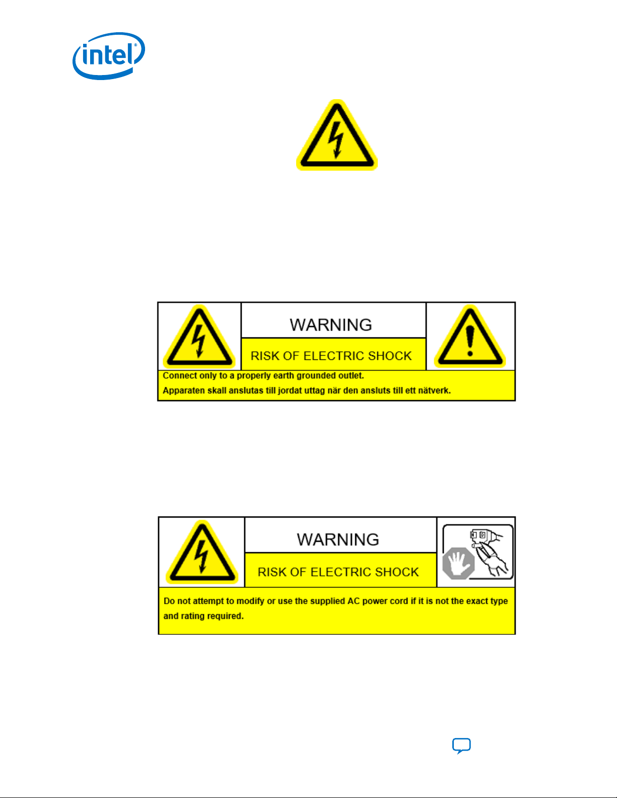
B. Safety and Regulatory Information
UG-20255 | 2020.11.16
Power Connect and Disconnect
The AC power supply cord is the primary disconnect device from mains (AC power)
and used to remove all DC power from the board/system. The socket outlet shall be
installed near the equipment and shall be readily accessible.
System Grounding (Earthing)
To avoid shock, ensure that the power cord is connected to a properly wired and
grounded receptacle. Ensure that any equipment to which this product is attached is
also connected to properly wired and grounded receptacles.
Power Cord Requirements
The connector that plugs into the wall outlet must be a grounding-type male plug
which is designed for use in your region. It must have certification marks showing
certification by an agency in your region. The connector that plugs into the AC
receptacle on the power supply must be an IEC 320, sheet C13, female connector. For
more information, refer to the website. If the power cord supplied with the system
does not meet requirements for use in your region discard the cord, do not use with
adapters.
Lightning or Electrical Storm
Do not connect or disconnect any cables or perform installation or maintenance of this
product during an electrical storm.
Intel® Stratix® 10 DX FPGA Development Kit User Guide
70
Send Feedback
Page 71

B. Safety and Regulatory Information
UG-20255 | 2020.11.16
Risk of Fire
To reduce the risk of fire, keep all flammable materials at a safe distance from the
boards and power supply and configure the development product on a flame-retardant
surface.
B.2. Safety Cautions
Thermal and Mechanical Injury
Certain components such as heat sinks, power regulators, and processors may be hot,
heatsink fans are not guarded, and power supply fan may be accessible through
guard. Care should be taken to avoid contact with these components.
Cooling Requirements
Maintain a minimum clearance area of 5 centimeters (2 inches) around the side, front,
and back of the development product for cooling purposes; do not block power supply
ventilation holes and fan.
Send Feedback
Intel® Stratix® 10 DX FPGA Development Kit User Guide
71
Page 72

B. Safety and Regulatory Information
UG-20255 | 2020.11.16
Electro Magnetic Interference
This equipment has not been tested for compliance with emission limits of FCC and
similar international regulations. Use of this equipment in a residential location is
prohibited. This equipment generates, uses and can radiate radio frequency energy,
which may result in harmful interference to radio communications. If this equipment
does cause harmful interference to radio or television reception, which can be
determined by turning the equipment on and off, take measures to eliminate the
interference.
Telecommunications Port Restrictions
The wireline telecommunication ports (modem, xDSL, T1/E1) on this product must not
be connected to the Public Switched Telecommunication Network (PSTN) as it might
result in disruption of the network. No formal telecommunication certification to FCC,
R&TTE Directive, or other national requirements has been obtained.
Electrostatic Discharge Warning
A properly grounded ESD wrist strap must be worn during operation/installation of the
boards, connection of cables, or during installation or removal of daughter cards.
Failure to do so can damage components within the system.
Please return this product to Intel for proper disposition. If it is not returned,
refer to the local environmental regulations for proper recycling; do not
dispose this product in any unsorted municipal waste.
Intel® Stratix® 10 DX FPGA Development Kit User Guide
72
Send Feedback
Page 73

UG-20255 | 2020.11.16
Send Feedback
C. Compliance and Conformity Information
CE EMI Conformity Caution
Hereby, Intel Corporation declares that the Intel Stratix 10 DX FPGA Development Kit
Board is in compliance with Directives 2014/30/EU, 2014/35/EU and 2011/65/EU.
Because of the nature of programmable logic devices, it is possible for the end user to
modify the development kit in such a way as to generate electromagnetic interference
(EMI) that exceeds the limits established for this equipment. Any caused as a result of
modifications to the delivered material is the responsibility of the user of this
development kit.
Att. Corp Quality, Intel Deutschland GmbH,
Am Campeon 10-12, Neubiberg, 85579 - Germany
For more information, refer to the EU declaration of conformity.
Intel Corporation. All rights reserved. Agilex, Altera, Arria, Cyclone, Enpirion, Intel, the Intel logo, MAX, Nios,
Quartus and Stratix words and logos are trademarks of Intel Corporation or its subsidiaries in the U.S. and/or
other countries. Intel warrants performance of its FPGA and semiconductor products to current specifications in
accordance with Intel's standard warranty, but reserves the right to make changes to any products and services
at any time without notice. Intel assumes no responsibility or liability arising out of the application or use of any
information, product, or service described herein except as expressly agreed to in writing by Intel. Intel
customers are advised to obtain the latest version of device specifications before relying on any published
information and before placing orders for products or services.
*Other names and brands may be claimed as the property of others.
ISO
9001:2015
Registered
 Loading...