

IS62WV5128ALL
®
IS62WV5128BLL
512K x 8 LOW VOLTAGE,
ULTRA LOW POWER CMOS STATIC RAM
FEATURES
• High-speed access time: 55ns, 70ns
• CMOS low power operation
36 mW (typical) operating
9 µW (typical) CMOS standby
• TTL compatible interface levels
• Single power supply
1.65V – 2.2V V
2.5V – 3.6V V
• Fully static operation: no clock or refresh
required
• Three state outputs
• Industrial temperature available
DD (IS62WV5128ALL)
DD (IS62WV5128BLL)
DESCRIPTION
The ISSI IS62WV5128ALL / IS62WV5128BLL are highspeed, 4M bit static RAMs organized as 512K words by 8
bits. It is fabricated using ISSI's high-performance CMOS
technology. This highly reliable process coupled with
innovative circuit design techniques, yields highperformance and low power consumption devices.
When CS1 is HIGH (deselected) the device assumes a
standby mode at which the power dissipation can be
reduced down with CMOS input levels.
Easy memory expansion is provided by using Chip Enable
and Output Enable inputs. The active LOW Write Enable
(WE) controls both writing and reading of the memory.
The IS62WV5128ALL and IS62WV5128BLL are packaged
in the JEDEC standard 32-pin TSOP (TYPE I), 32-pin
sTSOP (TYPE I), 32-pin TSOP (Type II), and 36-pin mini
BGA.
ISSI
MAY 2005
• Lead-free available
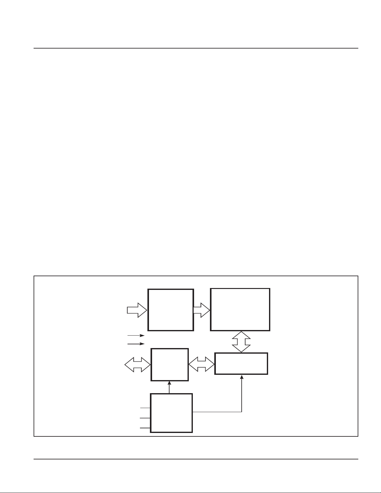
FUNCTIONAL BLOCK DIAGRAM
A0-A18
V
DD
GND
I/O0-I/O7
CS1
OE
WE
DECODER
I/O
DATA
CIRCUIT
CONTROL
CIRCUIT
512K x 8
MEMORY ARRAY
COLUMN I/O
Copyright © 2005 Integrated Silicon Solution, Inc. All rights reserved. ISSI reserves the right to make changes to this specification and its products at any time
without notice. ISSI assumes no liability arising out of the application or use of any information, products or services described herein. Customers are advised to
obtain the latest version of this device specification before relying on any published information and before placing orders for products.
Integrated Silicon Solution, Inc. — www.issi.com —
Rev. C
05/02/05
1-800-379-4774
1
IS62WV5128ALL, IS62WV5128BLL ISSI
PIN DESCRIPTIONS
A0-A18 Address Inputs
CS1 Chip Enable 1 Input
CS 2 Chip Enable 2 Input
OE Output Enable Input
WE Write Enable Input
I/O0-I/O7 Input/Output
N C No Connection
VDD Power
GND Ground
®
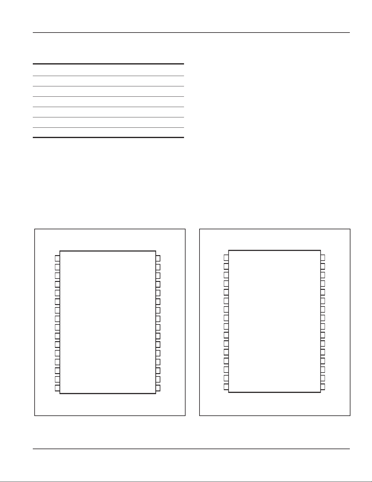
36-pin mini BGA (B) (6mm x 8mm)
(Package Code B)
1 2 3 4 5 6
A
B
C
D
E
F
G
H
A0
I/O4
I/O5
GND
VDD
I/O6
I/O7
A9
A1
A2
OE
A10
NC
WE
NC
A18
CS1
A11
A3
A4
A5
A17
A16
A12
A6
A7
A15
A13
A8
I/O0
I/O1
VDD
GND
I/O2
I/O3
A14
2
Integrated Silicon Solution, Inc. — www.issi.com —
1-800-379-4774
Rev. C
05/02/05
IS62WV5128ALL, IS62WV5128BLL ISSI
1
2
3
4
5
6
7
8
9
10
11
12
13
14
15
16
32
31
30
29
28
27
26
25
24
23
22
21
20
19
18
17
A17
A16
A14
A12
A7
A6
A5
A4
A3
A2
A1
A0
I/O0
I/O1
I/O2
GND
A15
A18
WE
A13
A8
A9
A11
OE
A10
CS1
I/O7
I/O6
I/O5
I/O4
I/O3
V
DD
PIN DESCRIPTIONS
A0-A18 Address Inputs
CS1 Chip Enable 1 Input
OE Output Enable Input
WE Write Enable Input
I/O0-I/O7 Input/Output
VDD Power
GND Ground
PIN CONFIGURATION
®
32-pin TSOP (TYPE I), (Package Code T)
32-pin sTSOP (TYPE I) (Package Code H)
1
A11
2
A9
3
A8
4
A13
5
WE
6
A18
7
A15
8
V
DD
9
A17
10
A16
11
A14
A12
A7
A6
A5
A4
12
13
14
15
16
Integrated Silicon Solution, Inc. — www.issi.com —
Rev. C
05/02/05
32
31
30
29
28
27
26
25
24
23
22
21
20
19
18
17
OE
A10
CS1
I/O7
I/O6
I/O5
I/O4
I/O3
GND
I/O2
I/O1
I/O0
A0
A1
A2
A3
32-pin TSOP (TYPE II)
(Package Code T2)
1-800-379-4774
3

IS62WV5128ALL, IS62WV5128BLL ISSI
OPERATING RANGE (VDD)
Range Ambient Temperature IS62WV5128ALL IS62WV5128BLL
Commercial 0°C to +70°C 1.65V - 2.2V 2.5V - 3.6V
Industrial –40°C to +85°C 1.65V - 2.2V 2.5V - 3.6V
®
ABSOLUTE MAXIMUM RATINGS
(1)
Symbol Parameter Value Unit
VTERM Terminal Voltage with Respect to GND –0.2 to VDD+0.3 V
VDD VDD Related to GND –0.2 to VDD+0.3 V
TSTG Storage Temperature –65 to +150 °C
PT Power Dissipation 1.0 W
Note:
1. Stress greater than those listed under ABSOLUTE MAXIMUM RATINGS may cause permanent damage to the device. This is
a stress rating only and functional operation of the device at these or any other conditions above those indicated in the
operational sections of this specification is not implied. Exposure to absolute maximum rating conditions for extended periods
may affect reliability.
DC ELECTRICAL CHARACTERISTICS (Over Operating Range)
Symbol Parameter Test Conditions VDD Min. Max. Unit
VOH Output HIGH Voltage IOH = -0.1 mA 1.65-2.2V 1.4 — V
IOH = -1 mA 2.5-3.6V 2. 2 — V
VOL Output LOW Voltage IOL = 0.1 mA 1.65-2.2V — 0.2 V
IOL = 2.1 mA 2.5-3.6V — 0.4 V
VIH Input HIGH Voltage 1.65-2.2V 1.4 VDD + 0.2 V
2.5-3.6V 2. 2 VDD + 0.3 V
(1)
VIL
ILI Input Leakage GND ≤ VIN ≤ VDD –1 1 µA
Input LOW Voltage 1.65-2.2V –0.2 0.4 V
2.5-3.6V –0.2 0.6 V
ILO Output Leakage GND ≤ VOUT ≤ VDD, Outputs Disabled – 1 1 µA
Notes:
1. VIL (min.) = –1.0V for pulse width less than 10 ns.
4
Integrated Silicon Solution, Inc. — www.issi.com —
1-800-379-4774
Rev. C
05/02/05
IS62WV5128ALL, IS62WV5128BLL ISSI
®
CAPACITANCE
(1)
Symbol Parameter Conditions Max. Unit
CIN Input Capacitance VIN = 0V 8 pF
COUT Input/Output Capacitance VOUT = 0V 1 0 pF
Note:
1. Tested initially and after any design or process changes that may affect these parameters.
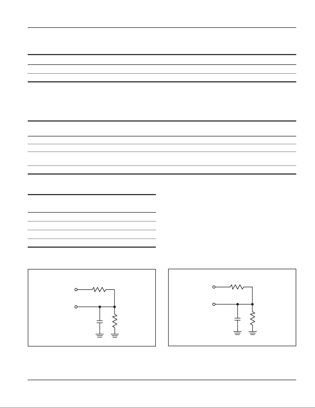
AC TEST CONDITIONS
Parameter IS62WV5128ALL IS62WV5128BLL
(Unit) (Unit)
Input Pulse Level 0.4V to VDD-0.2V 0.4V to VDD-0.3V
Input Rise and Fall Times 5 ns 5ns
Input and Output Timing VREF VREF
and Reference Level
Output Load See Figures 1 and 2 See Figures 1 and 2
IS62WV5128ALL IS62WV5128BLL
1.65 - 2.2V 2.5V - 3.6V
R1(Ω) 3070 3070
R2(Ω) 3150 3150
VREF 0.9V 1.5V
VTM 1.8V 2.8V
AC TEST LOADS
R1
VTM
OUTPUT
30 pF
Including
jig and
scope
Figure 1
R2
Figure 2
VTM
OUTPUT
5 pF
Including
jig and
scope
R1
R2
Integrated Silicon Solution, Inc. — www.issi.com —
Rev. C
05/02/05
1-800-379-4774
5

IS62WV5128ALL, IS62WV5128BLL ISSI
®
POWER SUPPLY CHARACTERISTICS
(1)
(Over Operating Range)
62WV5128ALL (1.65V - 2.2V)
Symbol Parameter Test Conditions Max. Unit
70 ns
ICC VDD Dynamic Operating VDD = Max., Com. 25 mA
Supply Current IOUT = 0 mA, f = fMAX Ind. 3 0
CC1 Operating Supply VDD = Max., CS1 = 0.2V Com. 10 mA
I
Current WE = VDD-0.2V Ind. 1 0
f=1MHZ
ISB1 TTL Standby Current VDD = Max., Com. 0.35 mA
(TTL Inputs) VIN = VIH or VIL Ind. 0.35
CS1 = VIH,
f = 1 MHZ
ISB2 CMOS Standby VDD = Max., Com. 15 µ A
Current (CMOS Inputs) CS1 ≥ VDD – 0.2V, Ind. 15
VIN ≥ VDD – 0.2V, or
VIN ≤ 0.2V, f = 0
Note:
1. At f = fMAX, address and data inputs are cycling at the maximum frequency, f = 0 means no input lines change.
POWER SUPPLY CHARACTERISTICS
(1)
(Over Operating Range)
62WV5128BLL (2.5V - 3.6V)
Symbol Parameter Test Conditions Max. Unit
55 ns
ICC VDD Dynamic Operating VDD = Max., Com. 40 mA
Supply Current IOUT = 0 mA, f = fMAX Ind. 45
ICC1 Operating Supply VDD = Max., CS1 = 0.2V Com. 15 mA
Current WE = VDD-0.2V Ind. 15
f=1MHZ
ISB1 TTL Standby Current VDD = Max., Com. 0.35 mA
(TTL Inputs) VIN = VIH or VIL Ind. 0.35
CS1 = VIH,
f = 1 MHZ
ISB2 CMOS Standby VDD = Max., Com. 15 µA
Current (CMOS Inputs) CS1 ≥ VDD – 0.2V, Ind. 1 5
VIN ≥ VDD – 0.2V, or
VIN ≤ 0.2V, f = 0
Note:
1. At f = f
MAX, address and data inputs are cycling at the maximum frequency, f = 0 means no input lines change.
6
Integrated Silicon Solution, Inc. — www.issi.com —
1-800-379-4774
Rev. C
05/02/05

IS62WV5128ALL, IS62WV5128BLL ISSI
®
READ CYCLE SWITCHING CHARACTERISTICS
(1)
(Over Operating Range)
55 ns 70 ns
Symbol Parameter Min. Max. Min. Max. Unit
tRC Read Cycle Time 55 — 70 — ns
tAA Address Access Time — 55 — 70 ns
tOHA Output Hold Time 10 — 10 — ns
tACS1 CS1 Access Time — 55 — 70 ns
tDOE OE Access Time — 25 — 35 ns
(2)
tHZOE
tLZOE
(2)
OE to High-Z Output — 20 — 25 ns
OE to Low-Z Output 5 — 5 — ns
tHZCS1 CS1 to High-Z Output 0 20 0 25 ns
tLZCS1 CS1 to Low-Z Output 10 — 10 — ns
Notes:
1. Test conditions assume signal transition times of 5 ns or less, timing reference levels of 0.9V/1.5V, input pulse levels of 0.4 to
VDD-0.2V/VDD-0.3V and output loading specified in Figure 1.
2. Tested with the load in Figure 2. Transition is measured ±500 mV from steady-state voltage. Not 100% tested.
AC WAVEFORMS
READ CYCLE NO. 1
ADDRESS
D
OUT
(1,2)
(Address Controlled) (CS1 = OE = VIL, WE = VIH)
t
RC
t
AA
t
OHA
PREVIOUS DATA VALID
t
OHA
DATA VALID
Integrated Silicon Solution, Inc. — www.issi.com —
Rev. C
05/02/05
1-800-379-4774
7

IS62WV5128ALL, IS62WV5128BLL ISSI
AC WAVEFORMS
READ CYCLE NO. 2
ADDRESS
OE
CS1
(1,3)
(CS1, OE Controlled)
t
ACS1
t
RC
t
AA
t
t
LZOE
DOE
t
HZOE
t
OHA
®
t
LZCS1
DOUT
Notes:
1. WE is HIGH for a Read Cycle.
2. The device is continuously selected. OE, CS1= V
3. Address is valid prior to or coincident with CS1 LOW transition.
HIGH-Z
IL. WE=VIH.
t
HZCS
DATA VALID
8
Integrated Silicon Solution, Inc. — www.issi.com —
1-800-379-4774
Rev. C
05/02/05

IS62WV5128ALL, IS62WV5128BLL ISSI
®
WRITE CYCLE SWITCHING CHARACTERISTICS
(1,2)
(Over Operating Range)
55 ns 70 ns
Symbol Parameter Min . Max. Min. Max. Unit
tWC Write Cycle Time 55 — 70 — ns
tSCS1 CS1 to Write End 45 — 60 — ns
tAW Address Setup Time to Write End 4 5 — 60 — ns
tHA Address Hold from Write End 0 — 0 — ns
tSA Address Setup Time 0 — 0 — ns
tPWE WE Pulse Width 40 — 50 — ns
tSD Data Setup to Write End 2 5 — 30 — ns
tHD Data Hold from Write End 0 — 0 — ns
(3)
tHZWE
(3)
tLZWE
Notes:
1. Test conditions assume signal transition times of 5 ns or less, timing reference levels of 0.9V/1.5V, input pulse levels of 0.4V to
V
DD-0.2V/VDD-0.3V and output loading specified in Figure 1.
The internal write time is defined by the overlap of CS1 LOW and WE LOW. All signals must be in valid states to initiate a Write, but any one can go inactive to
2.
terminate the Write. The Data Input Setup and Hold timing are referenced to the rising or falling edge of the signal that terminates the write.
3. Tested with the load in Figure 2. Transition is measured ±500 mV from steady-state voltage. Not 100% tested.
WE LOW to High-Z Output — 20 — 20 ns
WE HIGH to Low-Z Output 5 — 5 — ns
AC WAVEFORMS
WRITE CYCLE NO. 1 (CS1 Controlled, OE = HIGH or LOW)
t
WC
ADDRESS
t
SCS1
CS1
t
AW
t
WE
DOUT
DIN
t
SA
DATA UNDEFINED
t
HZWE
PWE
HIGH-Z
t
SD
DATA-IN VALID
t
HA
t
LZWE
t
HD
Integrated Silicon Solution, Inc. — www.issi.com —
Rev. C
05/02/05
1-800-379-4774
9

IS62WV5128ALL, IS62WV5128BLL ISSI
WRITE CYCLE NO. 2 (WE Controlled: OE is HIGH During Write Cycle)
t
WC
ADDRESS
OE
t
HA
t
t
LZWE
HD
CS1
WE
DOUT
t
SA
DATA UNDEFINED
t
AW
t
HZWE
t
SCS1
t
PWE
HIGH-Z
t
SD
®
DIN
DATA-IN VALID
WRITE CYCLE NO. 3 (WE Controlled: OE is LOW During Write Cycle)
t
WC
ADDRESS
OE
t
SCS1
CS1
t
AW
t
WE
PWE
t
HA
10
DOUT
DIN
t
SA
DATA UNDEFINED
t
HZWE
HIGH-Z
t
SD
DATA-IN VALID
t
LZWE
t
HD
Integrated Silicon Solution, Inc. — www.issi.com —
1-800-379-4774
Rev. C
05/02/05

IS62WV5128ALL, IS62WV5128BLL ISSI
DATA RETENTION SWITCHING CHARACTERISTICS
Symbol Parameter Test Condition Min. Max. Unit
VDR VDD for Data Retention See Data Retention Waveform 1.2 3.6 V
IDR Data Retention Current VDD = 1.2V, CS1 ≥ VDD – 0.2V — 1 5 µA
tSDR Data Retention Setup Time See Data Retention Waveform 0 — ns
tRDR Recovery Time See Data Retention Waveform tRC —ns
®
DATA RETENTION WAVEFORM (
t
SDR
V
DD
V
DR
CS1
GND
CS1CS1
CS1 Controlled)
CS1CS1
Data Retention Mode
CS1 ≥ V
DD -
0.2V
t
RDR
Integrated Silicon Solution, Inc. — www.issi.com —
Rev. C
05/02/05
1-800-379-4774
11

IS62WV5128ALL, IS62WV5128BLL ISSI
ORDERING INFORMATION
IS62WV5128ALL (1.65V-2.2V)
Industrial Range: –40°C to +85°C
Speed (ns) Order Part No. Package
70 IS62WV5128ALL-70TI TSOP, TYPE I
70 IS62WV5128ALL-70T2I TSOP, TYPE II
70 IS62WV5128ALL-70HI sTSOP, TYPE I
70 IS62WV5128ALL-70BI mini BGA (6mmx8mm)
ORDERING INFORMATION
IS62WV5128BLL (2.5V - 3.6V)
Commercial Range: 0°C to +70°C
®
Speed (ns) Order Part No. Package
55 IS62WV5128BLL-55H sTSOP, TYPE I
Industrial Range: –40°C to +85°C
Speed (ns) Order Part No. Package
55 IS62WV5128BLL-55TI TSOP, TYPE I
55 IS62WV5128BLL-55TLI TSOP, TYPE I, Lead-free
55 IS62WV5128BLL-55T2I TSOP, TYPE II
55 IS62WV5128BLL-55T2LI TSOP, TYPE II, Lead-free
55 IS62WV5128BLL-55HI sTSOP, TYPE I
55 IS62WV5128BLL-55HLI sTSOP, TYPE I, Lead-free
55 IS62WV5128BLL-55BI mini BGA (6mmx8mm)
55 IS62WV5128BLL-55BLI mini BGA (6mmx8mm), Lead-free
12
Integrated Silicon Solution, Inc. — www.issi.com —
1-800-379-4774
Rev. C
05/02/05

PACKAGING INFORMATION ISSI
Mini Ball Grid Array
Package Code: B (36-pin)
T op Vie w Bottom View
φ b (36x)
6 5 4 3 2 11 2 3 4 5 6
®
A
B
C
D
D
E
F
G
H
A2
mBGA - 6mm x 8mm
SEATING PLANE
A1
e
D1
Notes:
1. Controlling dimensions are in millimeters.
A
mBGA - 8mm x 10mm
A
B
C
D
E
F
G
H
e
E1E
MILLIMETERS INCHES
Sym. Min. Typ. Max. Min. Typ. Max.
N0.
Leads 36 36
A — — 1.20 — — 0.047
A1 0.24 — 0.30 0.009 — 0.012
A2 0.60 — — 0.024 — —
D 7.90 8.00 8.10 0.311 0.315 0.319
D1 5.25BSC 0.207BSC
E 5.90 6.00 6.10 0.232 0.236 0.240
E1 3.75BSC 0.148BSC
e 0.75BSC 0.030BSC
b 0.30 0.35 0.40 0.012 0.014 0.016
Copyright © 2003 Integrated Silicon Solution, Inc. All rights reserved. ISSI reserves the right to make changes to this specification and its products at any time
without notice. ISSI assumes no liability arising out of the application or use of any information, products or services described herein. Customers are advised to
obtain the latest version of this device specification before relying on any published information and before placing orders for products.
Integrated Silicon Solution, Inc. — www.issi.com —
Rev. E
01/15/03
Sym. Min. Typ. Max. Min. Typ. Max.
N0.
Leads 36 36
A — — 1.20 — — 0.047
A1 0.24 — 0.30 0.009 — 0.012
A2 0.60 — — 0.024 — —
D 9.90 10.00 10.10 0.390 0.394 0.398
D1 5.25BSC .207BSC
E 7.90 8.00 8.10 0.311 0.315 0.319
E1 3.7 5BSC 0.148BSC
e 0.75BSC 0.030BSC
b 0.30 0.35 0.40 0.012 0.014 0.016
1-800-379-4774
MILLIMETER INCHES

PACKAGING INFORMATION ISSI
Plastic TSOP-Type I
Package Code: T (32-pin)
1
E
H
®
N
D
S
e
B
MILLIMETERS INCHES
Symbol Min. Max. Min. Max.
No. Leads 32
A — 1.20 — 0.047
A1 0.05 0.25 0.002 0.010
B 0.17 0.23 0.007 0.009
C 0.12 0.17 0.005 0.007
D 7.90 8.10 0.311 0.319
E 18.30 18.50 0.720 0.728
H 19.80 20.20 0.780 0.795
e 0.50 BSC 0.020 BSC
L 0.40 0.60 0.016 0.024
α 0° 8° 0° 8°
S 0.25 REF 0.010 REF
A
A1
SEATING PLANE
L
Notes:
1. Controlling dimension: millimeters, unless
otherwise specified.
2. BSC = Basic lead spacing between centers.
3. Dimensions D and E do not include mold
flash protrusions and should be measured
from the bottom of the package.
4. Formed leads shall be planar with respect
to one another within 0.004 inches at the
seating plane.
α
C
Copyright © 2003 Integrated Silicon Solution, Inc. All rights reserved. ISSI reserves the right to make changes to this specification and its products at any time
without notice. ISSI assumes no liability arising out of the application or use of any information, products or services described herein. Customers are advised to
obtain the latest version of this device specification before relying on any published information and before placing orders for products.
Integrated Silicon Solution, Inc. — www.issi.com —
Rev. C
06/13/03
1-800-379-4774

PACKAGING INFORMATION ISSI
Plastic STSOP - 32 pins
Package Code: H (Type I)
A2
A
A1
®
1
N
E
b
e
D1
SEATING PLANE
S
D
L
α
C
Plastic STSOP (H - Type I)
Millimeters Inches
Symbol Min Max Min Max
Ref. Std.
N 32
A — 1.25 — 0.049
A1 0.05 — 0.002 —
A2 0.95 1.05 0.037 0.041
b 0.17 0.23 0.007 0.009
C 0.14 0.16 0.0055 0.0063
D 13.20 13.60 0.520 0.535
D1 11.70 11.90 0.461 0.469
E 7.90 8.10 0.311 0.319
e 0.50 BSC 0.020 BSC
L 0.30 0.70 0.012 0.028
S 0.28 Typ. 0.011 Typ.
α 0° 5° 0° 5°
Integrated Silicon Solution, Inc.
PK13197H32 Rev. B 04/21/03
Notes:
1. Controlling dimension: millimeters, unless otherwise
specified.
2. BSC = Basic lead spacing between centers.
3. Dimensions D1 and E do not include mold flash protrusions and
4. Formed leads shall be planar with respect to one another
within 0.004 inches at the seating plane.
should be measured from the bottom of the package
.

PACKAGING INFORMATION ISSI
Plastic TSOP
Package Code: T (Type II)
®
N/2+1N
E
E1
1
N/2
Notes:
1. Controlling dimension: millimieters,
unless otherwise specified.
2. BSC = Basic lead spacing
between centers.
3. Dimensions D and E1 do not
include mold flash protrusions and
should be measured from the
bottom of the package.
4. Formed leads shall be planar with
respect to one another within
0.004 inches at the seating plane.
D
SEATING PLANE
A
ZD
.
e
b
A1
L
α
C
Plastic TSOP (T - Type II)
Millimeters Inches Millimeters Inches Millimeters Inches
Symbol Min Max Min Max Min Max Min Max Min Max Min Max
Ref. Std.
No. Leads (N) 32 44 50
A — 1.20 — 0.047 — 1.20 — 0.047 — 1.20 — 0.047
A1 0.05 0.15 0.002 0.006 0.05 0.15 0.002 0.006 0.05 0.15 0.002 0.006
b 0.30 0.52 0.012 0.020 0.30 0.45 0.012 0.018 0.30 0.45 0.012 0.018
C 0.12 0.21 0.005 0.008 0.12 0.21 0.005 0.008 0.12 0.21 0.005 0.008
D 20.82 21.08 0.820 0.830 18.31 18.52 0.721 0.729 20.82 21.08 0.820 0.830
E1 10.03 10.29 0.391 0.400 10.03 10.29 0.395 0.405 10.03 10.29 0.395 0.405
E 11.56 11.96 0.451 0.466 11.56 11.96 0.455 0.471 11.56 11.96 0.455 0.471
e 1.27 BSC 0.050 BSC 0.80 BSC 0.032 BSC 0.80 BSC 0.031 BSC
L 0.40 0.60 0.016 0.024 0.41 0.60 0.016 0.024 0.40 0.60 0.016 0.024
ZD 0.95 REF 0.037 REF 0.81 REF 0.032 REF 0.88 REF 0.035 REF
α 0° 5° 0° 5° 0° 5° 0° 5° 0° 5° 0° 5°
Copyright © 2003 Integrated Silicon Solution, Inc. All rights reserved. ISSI reserves the right to make changes to this specification and its products at any time
without notice. ISSI assumes no liability arising out of the application or use of any information, products or services described herein. Customers are advised to
obtain the latest version of this device specification before relying on any published information and before placing orders for products.
Integrated Silicon Solution, Inc. — www.issi.com — 1-800-379-4774
Rev. F
06/18/03
 Loading...