

IS42S16100C1 ISSI
®
512K Words x 16 Bits x 2 Banks (16-MBIT)
SYNCHRONOUS DYNAMIC RAM
FEATURES
• Clock frequency: 200, 166, 143 MHz
• Fully synchronous; all signals referenced to a
positive clock edge
• Two banks can be operated simultaneously and
independently
• Dual internal bank controlled by A11
(bank select)
• Single 3.3V power supply
• LVTTL interface
• Programmable burst length
– (1, 2, 4, 8, full page)
• Programmable burst sequence:
Sequential/Interleave
• 4096 refresh cycles every 64 ms
• Random column address every clock cycle
• Programmable CAS latency (2, 3 clocks)
• Burst read/write and burst read/single write
operations capability
• Burst termination by burst stop and
precharge command
• Byte controlled by LDQM and UDQM
• Industrial temperature up to 143 MHz
• Packages 400-mil 50-pin TSOP-II, 60-ball fBGA
• Lead-free package option
DESCRIPTION
ISSI’s 16Mb Synchronous DRAM IS42S16100C1 is
organized as a 524,288-word x 16-bit x 2-bank for
improved performance. The synchronous DRAMs
achieve high-speed data transfer using pipeline
architecture. All inputs and outputs signals refer to the
rising edge of the clock input.
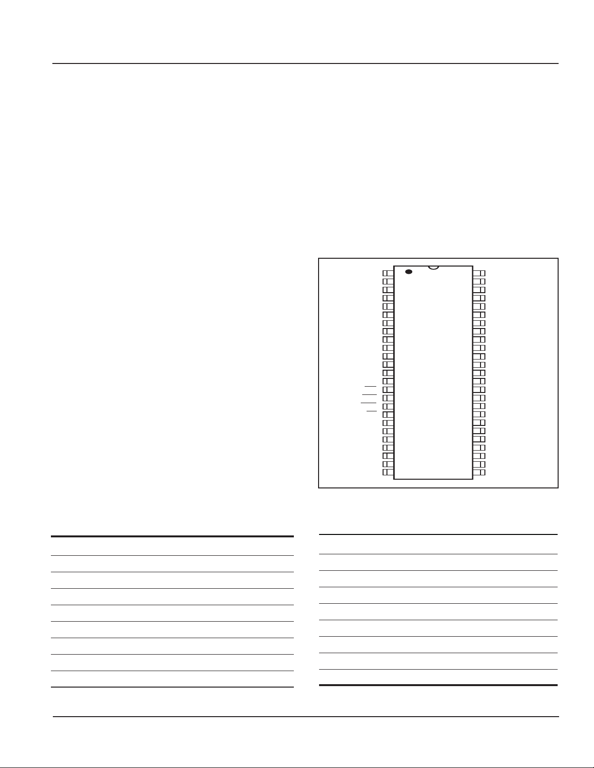
PIN CONFIGURATIONS
50-Pin TSOP (Type II)
VDD
DQ0
DQ1
GNDQ
DQ2
DQ3
VDDQ
DQ4
DQ5
GNDQ
DQ6
DQ7
VDDQ
LDQM
WE
CAS
RAS
CS
A11
A10
A0
A1
A2
A3
VDD
NOVEMBER 2006
1
2
3
4
5
6
7
8
9
10
11
12
13
14
15
16
17
18
19
20
21
22
23
24
25
50
GND
49
DQ15
48
IDQ14
47
GNDQ
46
DQ13
45
DQ12
44
VDDQ
43
DQ11
42
DQ10
41
GNDQ
40
DQ9
39
DQ8
38
VDDQ
37
NC
36
UDQM
35
CLK
34
CKE
33
NC
32
A9
31
A8
30
A7
29
A6
28
A5
27
A4
26
GND
PIN DESCRIPTIONS
A0-A11 Address Input
A0-A10 Row Address Input
A11 Bank Select Address
A0-A7 Column Address Input
DQ0 to DQ15 Data DQ
CLK System Clock Input
CKE Clock Enable
CS Chip Select
RAS Row Address Strobe Command
Copyright © 2006 Integrated Silicon Solution, Inc. All rights reserved. ISSI reserves the right to make changes to this specification and its products at any time
without notice. ISSI assumes no liability arising out of the application or use of any information, products or services described herein. Customers are advised to
obtain the latest version of this device specification before relying on any published information and before placing orders for products.
Integrated Silicon Solution, Inc. — www.issi.com —
Rev. D
11/03/06
1-800-379-4774
CAS Column Address Strobe Command
WE Write Enable
LDQM Lower Bye, Input/Output Mask
UDQM Upper Bye, Input/Output Mask
VDD Power
GND Ground
VDDQ Power Supply for DQ Pin
GNDQ Ground for DQ Pin
NC No Connection
1
IS42S16100C1 ISSI
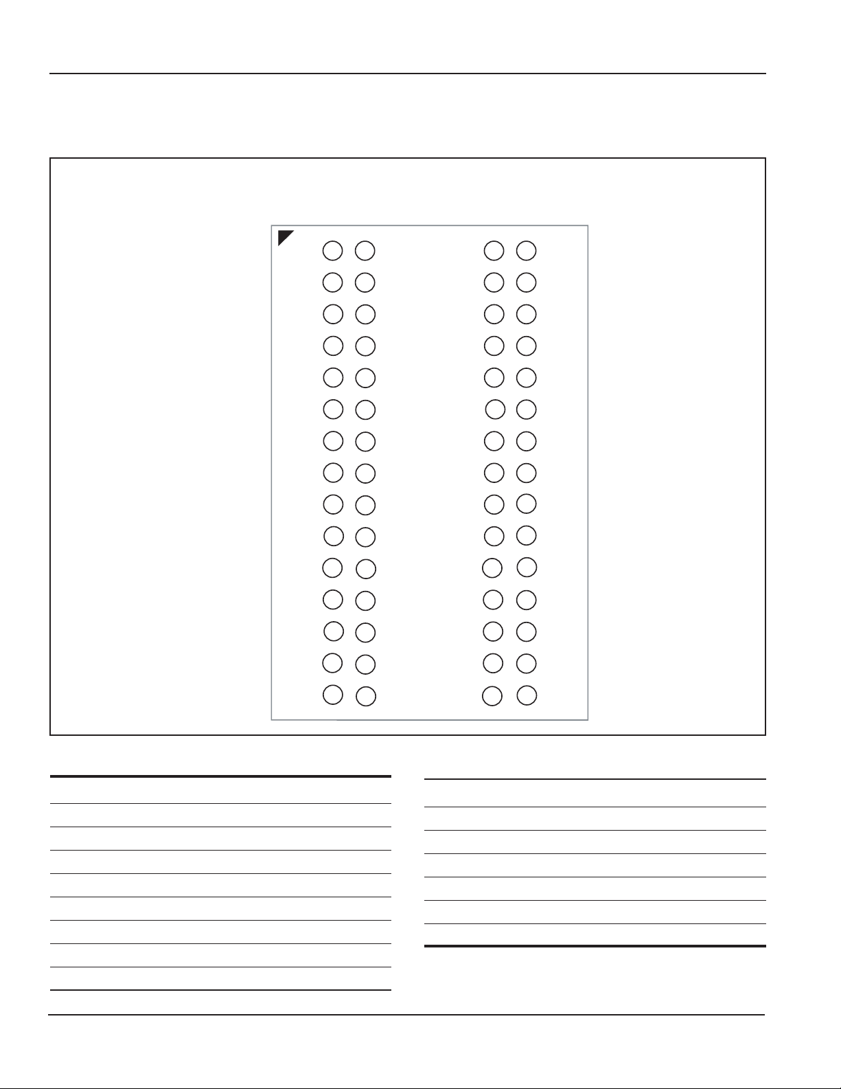
PIN CONFIGURATION
®
PACKAGE CODE:
B 60 BALL FBGA (Top View) (10.1 mm x 6.4 mm Body, 0.65 mm Ball Pitch)
1 2 3 4 5 6 7
A
VSS
DQ15
DQ0
VDD
B
DQ14
VSSQ
VDDQ
DQ1
C
DQ13
VDDQ
VSSQ
DQ2
D
DQ12
DQ11
DQ4
DQ3
E
DQ10
VSSQ
VDDQ
DQ5
F
DQ9
VDDQ
VSSQ
DQ6
G
DQ8
NC
NC
DQ7
H
NC
NC
NC
NC
J
NC
UDQM
LDQM
WE
K
NC
CLK
RAS
CAS
L
CKE
NC
NC
CS
M
A11
A9
NC
NC
N
A8
A7
A0
A10
P
A6
A5
A2
A1
R
VSS
A4
A3
VDD
PIN DESCRIPTIONS
A0-A10 Row Address Input
A0-A7 Column Address Input
A11 Bank Select Address
DQ0 to DQ15 Data I/O
CLK System Clock Input
CKE Clock Enable
CS Chip Select
RAS Row Address Strobe Command
CAS Column Address Strobe Command
2
Integrated Silicon Solution, Inc. — www.issi.com —
WE Write Enable
LDQM, UDQM x16 Input/Output Mask
VDD Power
Vss Ground
VDDQ Power Supply for I/O Pin
VssQ Ground for I/O Pin
NC No Connection
1-800-379-4774
Rev. D
11/03/06

®
IS42S16100C1 ISSI
PIN FUNCTIONS
Pin No. Symbol Type Function (In Detail)
20 to 24 A0-A10 Input Pin A0 to A10 are address inputs. A0-A10 are used as row address inputs during active
27 to 32 command input and A0-A7 as column address inputs during read or write command
input. A10 is also used to determine the precharge mode during other commands. If
A10 is LOW during precharge command, the bank selected by A11 is precharged,
but if A10 is HIGH, both banks will be precharged.
When A10 is HIGH in read or write command cycle, the precharge starts
automatically after the burst access.
These signals become part of the OP CODE during mode register set command
input.
19 A11 Input Pin A11 is the bank selection signal. When A11 is LOW, bank 0 is selected and when
high, bank 1 is selected. This signal becomes part of the OP CODE during mode
register set command input.
16 CAS Input Pin CAS, in conjunction with the RAS and WE, forms the device command. See the
“Command Truth Table” item for details on device commands.
34 CKE Input Pin The CKE input determines whether the CLK input is enabled within the device. When
is CKE HIGH, the next rising edge of the CLK signal will be valid, and when LOW,
invalid. When CKE is LOW, the device will be in either the power-down mode, the
clock suspend mode, or the self refresh mode. The CKE is an asynchronous input.
35 CLK Input Pin CLK is the master clock input for this device. Except for CKE, all inputs to this device
are acquired in synchronization with the rising edge of this pin.
18 CS Input Pin The CS input determines whether command input is enabled within the device.
Command input is enabled when CS is LOW, and disabled with CS is HIGH. The
device remains in the previous state when CS is HIGH.
2, 3, 5, 6, 8, 9, 11 DQ0 to DQ Pin DQ0 to DQ15 are DQ pins. DQ through these pins can be controlled in byte units
12, 39, 40, 42, 43, DQ15 using the LDQM and UDQM pins.
45, 46, 48, 49
14, 36 LDQM, Input Pin LDQM and UDQM control the lower and upper bytes of the DQ buffers. In read
UDQM mode, LDQM and UDQM control the output buffer. When LDQM or UDQM is LOW,
the corresponding buffer byte is enabled, and when HIGH, disabled. The outputs go
to the HIGH impedance state when LDQM/UDQM is HIGH. This function
corresponds to OE in conventional DRAMs. In write mode, LDQM and UDQM control
the input buffer. When LDQM or UDQM is LOW, the corresponding buffer byte is
enabled, and data can be written to the device. When LDQM or UDQM is HIGH, input
data is masked and cannot be written to the device.
17 RAS Input Pin RAS, in conjunction with CAS and WE, forms the device command. See the
“Command Truth Table” item for details on device commands.
15 WE Input Pin WE, in conjunction with RAS and CAS, forms the device command. See the
“Command Truth Table” item for details on device commands.
7, 13, 38, 44 VDDQ Power Supply Pin VDDQ is the output buffer power supply.
1, 25 VDD Power Supply Pin VDD is the device internal power supply.
4, 10, 41, 47 GND Q Power Supply Pin GNDQ is the output buffer ground.
26, 50 GND Power Supply Pin GND is the device internal ground.
Integrated Silicon Solution, Inc. — www.issi.com —
Rev. D
11/03/06
1-800-379-4774
3
IS42S16100C1 ISSI
5
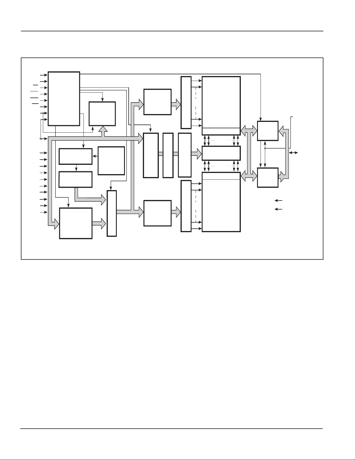
FUNCTIONAL BLOCK DIAGRAM
CLK
CKE
CS
RAS
CAS
WE
A11
COMMAND
DECODER
&
CLOCK
GENERATOR
MODE
REGISTER
11
ROW
ADDRESS
BUFFER
11
2048
MEMORY CELL
ARRAY
BANK 0
DQM
®
A10
A9
A8
A7
A6
A5
A4
A3
A2
A1
A0
REFRESH
CONTROLLER
REFRESH
COUNTER
ADDRESS
LATCH
11
ROW
11
SELF
REFRESH
CONTROLLER
MULTIPLEXER
8
11
COLUMN
ADDRESS LATCH
ROW
ADDRESS
BUFFER
COLUMN
BURST COUNTER
11
ADDRESS BUFFER
2048
ROW DECODER ROW DECODER
SENSE AMP I/O GATE
256
COLUMN DECODER
8
256
SENSE AMP I/O GATE
MEMORY CELL
ARRAY
BANK 1
DATA IN
BUFFER
16
DATA OUT
BUFFER
16 16
16
DQ 0-1
VDD/VDDQ
GND/GNDQ
S16BLK.eps
4
Integrated Silicon Solution, Inc. — www.issi.com —
1-800-379-4774
Rev. D
11/03/06

IS42S16100C1 ISSI
®
ABSOLUTE MAXIMUM RATINGS
(1)
Symbol Parameters Rating Unit
VDD MAX Maximum Supply Voltage –1.0 to +4.6 V
VDDQ
MAX Maximum Supply Voltage for Output Buffer –1.0 to +4.6 V
VIN Input Voltage –1.0 to +4.6 V
VOUT Output Voltage –1.0 to +4.6 V
PD MAX Allowable Power Dissipation 1 W
ICS Output Shorted Current 50 mA
TOPR Operating Temperature Com 0 to +70 °C
Ind. -40 to +85 °C
TSTG Storage Temperature –55 to +150 °C
DC RECOMMENDED OPERATING CONDITIONS
(2)
(At TA = 0 to +70°C)
Symbol Parameter Min. Typ. Max. Unit
VDD, VDDQ Supply Voltage 3.0 3.3 3.6 V
VIH Input High Voltage
VIL Input Low Voltage
(3)
(4)
2.0 — VDD + 0.3 V
-0.3 — +0.8 V
CAPACITANCE CHARACTERISTICS
(1,2)
(At TA = 0 to +25°C, VDD = VDDQ = 3.3 ± 0.3V, f = 1 MHz)
Symbol Parameter Typ. Max. Unit
CIN1 Input Capacitance: A0-A11 — 4 pF
CIN2 Input Capacitance: (CLK, CKE, CS, RAS, CAS, WE, LDQM, UDQM) — 4 pF
CI/O Data Input/Output Capacitance: DQ0-DQ15 — 5 pF
Notes:
1. Stress greater than those listed under ABSOLUTE MAXIMUM RATINGS may cause permanent damage to the device. This
is a stress rating only and functional operation of the device at these or any other conditions above those indicated in the
operational sections of this specification is not implied. Exposure to absolute maximum rating conditions for extended
periods may affect reliability.
2. All voltages are referenced to GND.
3. VIH (max) = VDDQ + 2.0V with a pulse width ≤ 3 ns.
Integrated Silicon Solution, Inc. — www.issi.com —
Rev. D
11/03/06
1-800-379-4774
5

®
IS42S16100C1 ISSI
DC ELECTRICAL CHARACTERISTICS (Recommended Operation Conditions unless otherwise noted.)
Symbol Parameter Test Condition Speed Min. Max. Unit
IIL Input Leakage Current 0V ≤ VIN ≤ VDD, with pins other than –5 5 µA
the tested pin at 0V
IOL Output Leakage Current Output is disabled, 0V ≤ VOUT ≤ VDD –5 5 µA
VOH Output High Voltage Level IOUT = –2 mA 2.4 — V
VOL Output Low Voltage Level IOUT = +2 mA — 0.4 V
ICC1 Operating Current
ICC2P Precharge Standby CurrentCKE ≤ VIL (MAX)tCK = tCK (MIN) Com. — — 3 mA
ICC2PS (In Power-Down Mode) tCK = ∞ Com. — — 2 mA
ICC3N Active Standby Current CKE ≥ VIH (MIN)tCK = tCK (MIN)——40mA
ICC3NS (In Non Power-Down Mode) tCK = ∞ Com. — — 30 mA
ICC4 Operating Current tCK = tCK (MIN) CAS latency = 3 Com. -5 — 170 mA
(In Burst Mode)
ICC5 Auto-Refresh Current tRC = tRC (MIN) CAS latency = 3 Com. -5 — 120 mA
ICC6 Self-Refresh Current CKE ≤ 0.2V — — 1 mA
Notes:
1. These are the values at the minimum cycle time. Since the currents are transient, these values decrease as the cycle time
increases. Also note that a bypass capacitor of at least 0.01 µF should be inserted between VDD and GND for each
memory chip to suppress power supply voltage noise (voltage drops) due to these transient currents.
2. Icc1 and Icc4 depend on the output load. The maximum values for Icc1 and Icc4 are obtained with the output open state.
(1,2)
One Bank Operation, CAS latency = 3 Com. -5 — 170 mA
Burst Length=1 Com. -6 — 160 mA
tRC ≥ tRC (min.) Com. -7 — 140 mA
IOUT = 0mA Ind. -7 — 160 mA
Ind. — — 4 mA
Ind. — — 3 mA
Ind. — — 30 mA
(1)
IOUT = 0mA Com. -6 — 150 mA
Com. -7 — 130 mA
Ind. -7 — 150 mA
CAS latency = 2 Com. -5 — 170 mA
Com. -6 — 150 mA
Com. -7 — 130 mA
Ind. -7 — 150 m
Com. -6 — 100 mA
Com. -7 — 70 mA
Ind. -7 — 90 mA
CAS latency = 2 Com. -5 — 120 mA
Com. -6 — 100 mA
Com. -7 — 70 mA
Ind. -7 — 90 mA
6
Integrated Silicon Solution, Inc. — www.issi.com —
1-800-379-4774
Rev. D
11/03/06

IS42S16100C1 ISSI
®
AC CHARACTERISTICS
(1,2,3)
-5 -6 -7
Symbol Parameter
Min. Max. Min. Max. Min. Max. Units
tCK3 Clock Cycle Time CAS Latency = 3 5 — 6 — 7 — ns
tCK2 CAS Latency = 2 8 — 8 — 8 — ns
tAC3 Access Time From CLK
(4)
CAS Latency = 3 — 5 — 5.5 — 5.5 ns
tAC2 CAS Latency = 2 — 6 — 6 — 6 ns
tCHI CLK HIGH Level Width 2 — 2.5 — 2.5 — ns
tCL CLK LOW Level Width 2 — 2.5 — 2.5 — ns
tOH3 Output Data Hold Time CAS Latency = 3 2 — 2.0 — 2.0 — ns
tOH2 CAS Latency = 2 2.5 — 2.5 — 2.5 — ns
tLZ Output LOW Impedance Time 0 — 0 — 0 — ns
tHZ3 Output HIGH Impedance Time(5) CAS Latency = 3 — 4 — 5.5 — 5.5 ns
tHZ2 CAS Latency = 2 — 6 — 6 — 6 ns
tDS Input Data Setup Time 1.5 — 1.5 — 2 — ns
tDH Input Data Hold Time 1 — 1 — 1 — ns
tAS Address Setup Time 1.5 — 1.5 — 2 — ns
tAH Address Hold Time 1 — 1 — 1 — ns
tCKS CKE Setup Time 1.5 — 1.5 — 2 — ns
tCKH CKE Hold Time 1 — 1 — 1 — ns
tCKA CKE to CLK Recovery Delay Time 1CLK+3 — 1CLK+3 —1CLK+3
—ns
tCS Command Setup Time (CS, RAS, CAS, WE, DQM) 1.5 — 1.5 — 2 — ns
tCH Command Hold Time (CS, RAS, CAS, WE, DQM) 1 — 1 — 1 — ns
tRC Command Period (REF to REF / ACT to ACT) 48 — 54 — 63 — ns
tRAS Command Period (ACT to PRE) 32 — 36 100,000 42 100,000 ns
tRP Command Period (PRE to ACT) 16 — 18 — 20 — ns
tRCD Active Command To Read / Write Command Delay Time 16 — 16 — 16 — ns
tRRD Command Period (ACT [0] to ACT[1]) 11 — 12 — 14 — ns
tDPL3 Input Data To Precharge CAS Latency = 3 — 1CLK 1CLK — 1CLK — ns
Command Delay time
tDPL2 CAS Latency = 2 — 1CLK 1CLK — 1CLK — ns
tDAL3 Input Data To Active / Refresh CAS Latency = 3 1CLK+tRP — 1CLK+tRP — 1CLK+tRP —ns
Command Delay time (During Auto-Precharge)
tDAL2 CAS Latency = 2 1CLK+tRP — 1CLK+tRP — 1CLK+tRP —ns
tT Transition Time 1 10 1 10 1 10 ns
tREF Refresh Cycle Time (4096) — 64 — 64 — 64 ms
Notes:
1. When power is first applied, memory operation should be started 100 µs after V
sequence must be executed before starting memory operation.
2. Measured with tT = 1 ns.
3. The reference level is 1.4 V when measuring input signal timing. Rise and fall times are measured between V
4. Access time is measured at 1.4V with the load shown in the figure below.
5. The time t
output is in the high impedance state.
HZ
(max.) is defined as the time required for the output voltage to transition by ± 200 mV from V
DD
and V
DDQ
reach their stipulated voltages. Also note that the power-on
IH
(min.) and VIL (max.).
OH
(min.) or VOL (max.) when the
Integrated Silicon Solution, Inc. — www.issi.com —
Rev. D
11/03/06
1-800-379-4774
7
IS42S16100C1 ISSI
OPERATING FREQUENCY / LATENCY RELATIONSHIPS
SYMBOL PARAMETER -5 -6 -7 UNITS
— Clock Cycle Time 5 6 7 ns
— Operating Frequency 200 166 143 MHz
tCAC CAS Latency 3 3 3 cycle
tRCD Active Command To Read/Write Command Delay Time 3 3 3 cycle
tRAC RAS Latency (tRCD + tCAC) 6 6 6 cycle
tRC Command Period (REF to REF / ACT to ACT) 9 9 9 cycle
tRAS Command Period (ACT to PRE) 6 6 6 cycle
tRP Command Period (PRE to ACT) 3 3 3 cycle
tRRD Command Period (ACT[0] to ACT [1]) 3 3 3 cycle
tCCD Column Command Delay Time 1 1 1 cycle
(READ, READA, WRIT, WRITA)
tDPL Input Data To Precharge Command Delay Time 1 1 1 cycle
®
tDAL Input Data To Active/Refresh Command Delay Time 4 4 4 cycle
(During Auto-Precharge)
tRBD Burst Stop Command To Output in HIGH-Z Delay Time 3 3 3 cycle
(Read)
tWBD Burst Stop Command To Input in Invalid Delay Time 0 0 0 cycle
(Write)
tRQL Precharge Command To Output in HIGH-Z Delay Time 3 3 3 cycle
(Read)
tWDL Precharge Command To Input in Invalid Delay Time 0 0 0 cycle
(Write)
tPQL Last Output To Auto-Precharge Start Time (Read) -2 –2 –1 cycle
tQMD DQM To Output Delay Time (Read) 2 2 2 cycle
tDMD DQM To Input Delay Time (Write) 0 0 0 cycle
tMCD Mode Register Set To Command Delay Time 2 2 2 cycle
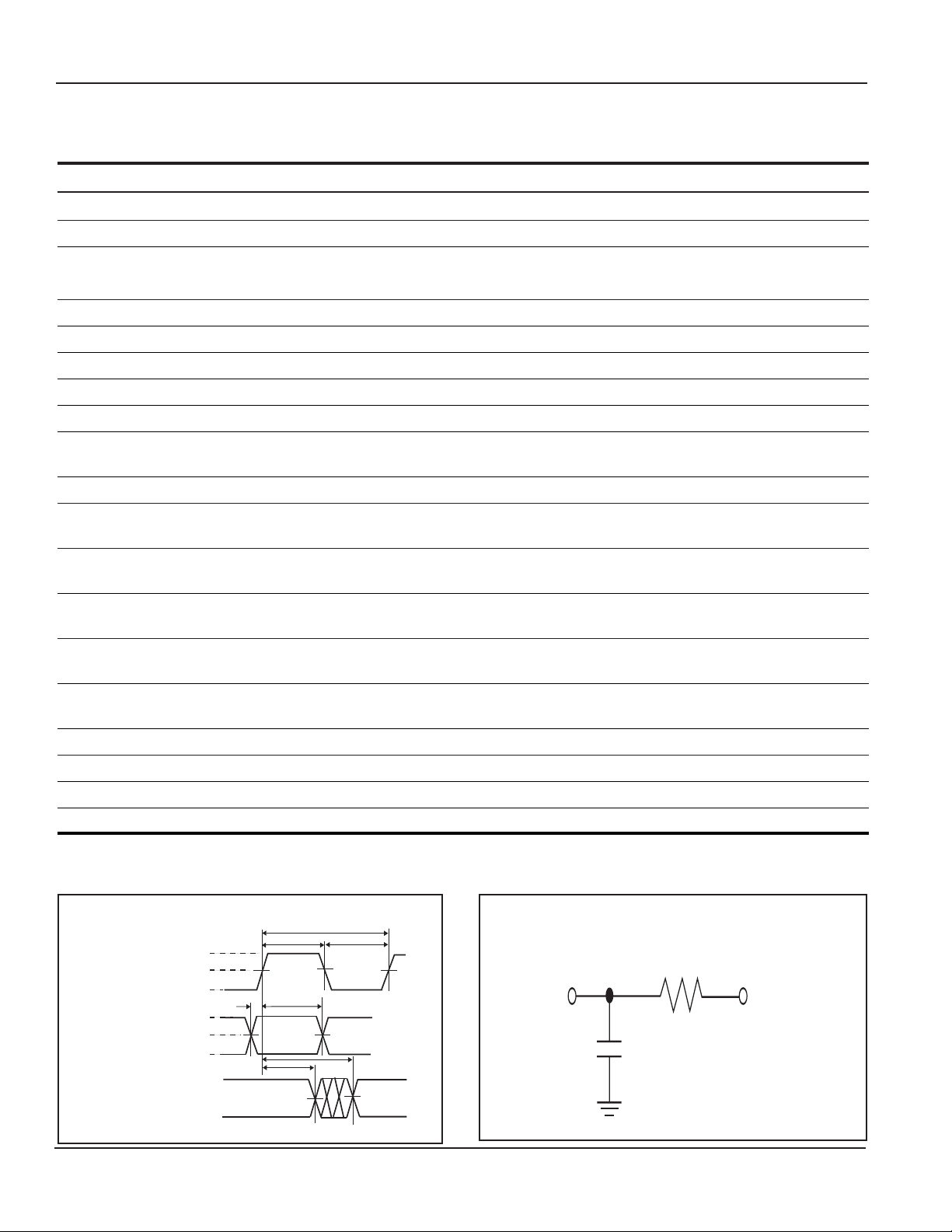
AC TEST CONDITIONS (Input/Output Reference Level: 1.4V)
Input
CLK
INPUT
2.8V
1.4V
0.0V
2.8V
1.4V
0.0V
tCS
tOH
tCHI
tCH
tCK
tCL
tAC
Output Load
I/O
50 Ω
+1.4V
50 pF
OUTPUT
1.4V
8
1.4V
Integrated Silicon Solution, Inc. — www.issi.com —
1-800-379-4774
Rev. D
11/03/06
IS42S16100C1 ISSI
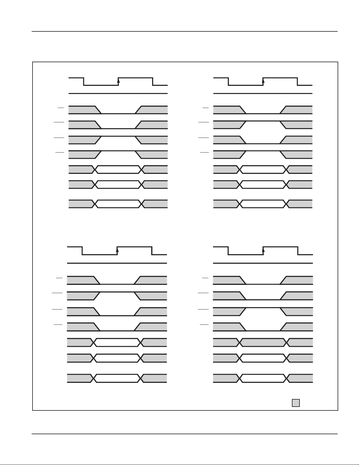
COMMANDS
Active Command Read Command
®
CLK
CKE
CS
RAS
CAS
WE
A0-A9
A10
A11
HIGH
ROW
ROW
BANK 1
BANK 0
CLK
CKE
CS
RAS
CAS
WE
A0-A9
A10
A11
HIGH
COLUMN
AUTO PRECHARGE
NO PRECHARGE
BANK 1
BANK 0
Write Command Precharge Command
CLK
CLK
(1)
HIGH
CKE
CS
RAS
CAS
WE
A0-A9
A10
A11
Notes:
1. A8-A9 = Don’t Care.
COLUMN
AUTO PRECHARGE
(1)
BANK 1
BANK 0
CKE
CS
RAS
CAS
WE
A0-A9
A10
A11
HIGH
BANK 0 AND BANK 1
BANK 0 OR BANK 1NO PRECHARGE
BANK 1
BANK 0
Don't Care
Integrated Silicon Solution, Inc. — www.issi.com —
Rev. D
11/03/06
1-800-379-4774
9
IS42S16100C1 ISSI
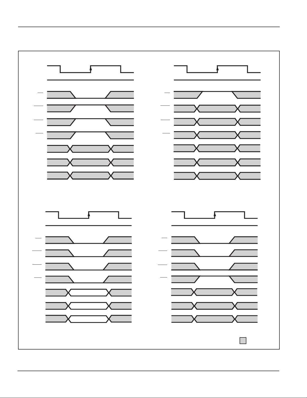
COMMANDS (cont.)
No-Operation Command Device Deselect Command
®
CLK
CKE
CS
RAS
CAS
WE
A0-A9
A10
A11
HIGH
CLK
CKE
CS
RAS
CAS
WE
A0-A9
A10
A11
HIGH
Mode Register Set Command Auto-Refresh Command
CLK
CKE
CS
RAS
CAS
WE
A0-A9
A10
A11
HIGH
OP-CODE
OP-CODE
OP-CODE
CLK
CKE
CS
RAS
CAS
WE
A0-A9
A10
A11
HIGH
Don't Care
10
Integrated Silicon Solution, Inc. — www.issi.com —
1-800-379-4774
Rev. D
11/03/06
IS42S16100C1 ISSI
COMMANDS (cont.)
Self-Refresh Command Power Down Command
®
CLK
CKE
CS
RAS
CAS
WE
A0-A9
A10
A11
CLK
CKE
CS
RAS
CAS
WE
A0-A9
A10
A11
ALL BANKS IDLE
NOP
NOP
NOP
NOP
Clock Suspend Command Burst Stop Command
CLK
BANK(S) ACTIVE
CKE
CS
RAS
CAS
WE
A0-A9
A10
A11
NOP
NOP
NOP
NOP
Integrated Silicon Solution, Inc. — www.issi.com —
Rev. D
11/03/06
CLK
CKE
CS
RAS
CAS
WE
A0-A9
A10
A11
1-800-379-4774
HIGH
11

IS42S16100C1 ISSI
Mode Register Set Command
(CS, RAS, CAS, WE = LOW)
The IS42S16100C1 product incorporates a register that
defines the device operating mode. This command
functions as a data input pin that loads this register from
the pins A0 to A11. When power is first applied, the
stipulated power-on sequence should be executed and
then the IS42S16100C1 should be initialized by executing
a mode register set command.
Note that the mode register set command can be executed
only when both banks are in the idle state (i.e. deactivated).
Another command cannot be executed after a mode
register set command until after the passage of the period
tMCD, which is the period required for mode register set
command execution.
Active Command
(CS, RAS = LOW, CAS, WE= HIGH)
The IS42S16100C1 includes two banks of 4096 rows
each. This command selects one of the two banks
according to the A11 pin and activates the row selected
by the pins A0 to A10.
This command corresponds to the fall of the RAS signal
from HIGH to LOW in conventional DRAMs.
When the A10 pin is HIGH, this command functions as a
read with auto-precharge command. After the burst read
completes, the bank selected by pin A11 is precharged.
When the A10 pin is LOW, the bank selected by the A11 pin
remains in the activated state after the burst read completes.
Write Command
(CS, CAS, WE = LOW, RAS = HIGH)
When burst write mode has been selected with the mode
register set command, this command selects the bank
specified by the A11 pin and starts a burst write operation
at the start address specified by pins A0 to A9. This first
data must be input to the DQ pins in the cycle in which this
command.
The selected bank must be activated before executing this
command.
When A10 pin is HIGH, this command functions as a write
with auto-precharge command. After the burst write
completes, the bank selected by pin A11 is precharged.
When the A10 pin is low, the bank selected by the A11 pin
remains in the activated state after the burst write completes.
After the input of the last burst write data, the application
must wait for the write recovery period (tDPL, tDAL) to elapse
according to CAS latency.
®
Precharge Command
(CS, RAS, WE = LOW, CAS = HIGH)
This command starts precharging the bank selected by
pins A10 and A11. When A10 is HIGH, both banks are
precharged at the same time. When A10 is LOW, the bank
selected by A11 is precharged. After executing this
command, the next command for the selected bank(s) is
executed after passage of the period tRP, which is the
period required for bank precharging.
This command corresponds to the RAS signal from LOW
to HIGH in conventional DRAMs
Read Command
(CS, CAS = LOW, RAS, WE = HIGH)
This command selects the bank specified by the A11 pin
and starts a burst read operation at the start address
specified by pins A0 to A9. Data is output following CAS
latency.
The selected bank must be activated before executing
this command.
Auto-Refresh Command
(CS, RAS, CAS = LOW, WE, CKE = HIGH)
This command executes the auto-refresh operation. The
row address and bank to be refreshed are automatically
generated during this operation.
Both banks must be placed in the idle state before executing
this command.
The stipulated period (tRC) is required for a single refresh
operation, and no other commands can be executed during
this period.
The device goes to the idle state after the internal refresh
operation completes.
This command must be executed at least 4096 times every
128 ms.
This command corresponds to CBR auto-refresh in
conventional DRAMs.
12
Integrated Silicon Solution, Inc. — www.issi.com —
1-800-379-4774
Rev. D
11/03/06

IS42S16100C1 ISSI
®
Self-Refresh Command
(CS, RAS, CAS, CKE = LOW, WE = HIGH)
This command executes the self-refresh operation. The
row address to be refreshed, the bank, and the refresh
interval are generated automatically internally during this
operation. The self-refresh operation is started by dropping
the CKE pin from HIGH to LOW. The self-refresh operation
continues as long as the CKE pin remains LOW and there
is no need for external control of any other pins. The
self-refresh operation is terminated by raising the CKE pin
from LOW to HIGH. The next command cannot be executed
until the device internal recovery period (tRC) has elapsed.
After the self-refresh, since it is impossible to determine
the address of the last row to be refreshed, an auto-refresh
should immediately be performed for all addresses (4096
cycles).
Both banks must be placed in the idle state before
executing this command.
Burst Stop Command
(CS, WE, = LOW, RAS, CAS = HIGH)
The command forcibly terminates burst read and write
operations. When this command is executed during a
burst read operation, data output stops after the CAS
latency period has elapsed.
No Operation
(CS, = LOW, RAS, CAS, WE = HIGH)
This command has no effect on the device.
Device Deselect Command
(CS = HIGH)
This command does not select the device for an object of
operation. In other words, it performs no operation with
respect to the device.
Power-Down Command
(CKE = LOW)
When both banks are in the idle (inactive) state, or when
at least one of the banks is not in the idle (inactive) state,
this command can be used to suppress device power
dissipation by reducing device internal operations to the
absolute minimum. Power-down mode is started by dropping
the CKE pin from HIGH to LOW. Power-down mode
continues as long as the CKE pin is held low. All pins other
than the CKE pin are invalid and none of the other
commands can be executed in this mode. The powerdown operation is terminated by raising the CKE pin from
LOW to HIGH. The next command cannot be executed
until the recovery period (t
Since this command differs from the self-refresh command
described above in that the refresh operation is not
performed automatically internally, the refresh operation
must be performed within the refresh period (tREF). Thus
the maximum time that power-down mode can be held is
just under the refresh cycle time.
CKA) has elapsed.
Clock Suspend
(CKE = LOW)
This command can be used to stop the device internal
clock temporarily during a read or write cycle. Clock
suspend mode is started by dropping the CKE pin from
HIGH to LOW. Clock suspend mode continues as long as
the CKE pin is held LOW. All input pins other than the CKE
pin are invalid and none of the other commands can be
executed in this mode. Also note that the device internal
state is maintained. Clock suspend mode is terminated by
raising the CKE pin from LOW to HIGH, at which point
device operation restarts. The next command cannot be
executed until the recovery period (tCKA) has elapsed.
Since this command differs from the self-refresh command
described above in that the refresh operation is not
performed automatically internally, the refresh operation
must be performed within the refresh period (tREF). Thus
the maximum time that clock suspend mode can be held
is just under the refresh cycle time.
Integrated Silicon Solution, Inc. — www.issi.com —
Rev. D
11/03/06
1-800-379-4774
13

IS42S16100C1 ISSI
®
COMMAND TRUTH TABLE
(1,2)
CKE
CSCS
RASRAS
CASCAS
Symbol Command n-1 n
(5)
(5,6)
(3,4)
HXLLLLX OP CODE X
H H L L L H X X X X HIGH-Z
HLLLLHXX X XHIGH-Z
MRS Mode Register Set
REF Auto-Refresh
SREF Self-Refresh
CS
CSCS
RAS
RASRAS
WEWE
CAS
WEDQM A11 A10 A9-A0 I/On
CASCAS
WEWE
PRE Precharge Selected Bank H X L L H L X BS L X X
PALL Precharge Both Banks H X L L H L X X H X X
ACT Bank Activate
WRIT Write H X L H L L X BS L Column
WRITA Write With Auto-Precharge
READ Read
(8)
READA Read With Auto-Precharge
BST Burst Stop
(7)
(8)
(8)
(9)
H X L L H H X BS Row Row X
(18)
H X L H L L X BS H Column
H X L H L H X BS L Column
H X L H L H X BS H Column
(18)
(18)
(18)
HXLHHLXXXX X
NOP No Operation H X L HHHXX X X X
DESL Device Deselect H X H XXXXX X X X
SBY Clock Suspend / Standby Mode L XXXXXXX X X X
ENB Data Write / Output Enable H XXXXXLX X X Active
MASK Data Mask / Output Disable H XXXXXHX X XHIGH-Z
X
X
X
X
DQM TRUTH TABLE
(1,2)
CKE DQM
Symbol Command n-1 n UPPER LOWER
ENB Data Write / Output Enable H X L L
MASK Data Mask / Output Disable H X H H
ENBU Upper Byte Data Write / Output Enable H X L X
ENBL Lower Byte Data Write / Output Enable H X X L
MASKU Upper Byte Data Mask / Output Disable H X H X
MASKL Lower Byte Data Mask / Output Disable H X X H
CKE TRUTH TABLE
(1,2)
CKE
CSCS
RASRAS
CASCAS
Symbol Command Current State n-1 n
CS
CSCS
RAS
RASRAS
WEWE
CAS
WE A11 A10 A9-A0
CASCAS
WEWE
SPND Start Clock Suspend Mode Active H L XXXXXXX
— Clock Suspend Other States L L XXXXXXX
— Terminate Clock Suspend Mode Clock Suspend L H XXXXXXX
REF Auto-Refresh Idle H H L L L H X X X
SELF Start Self-Refresh Mode Idle H LLLLHXXX
SELFX Terminate Self-Refresh Mode Self-Refresh L H L HHHXXX
LHHXXXXXX
PDWN Start Power-Down Mode Idle H L L HHHXXX
HLHXXXXXX
— Terminate Power-Down Mode Power-Down L H XXXXXXX
14
Integrated Silicon Solution, Inc. — www.issi.com —
1-800-379-4774
Rev. D
11/03/06

IS42S16100C1 ISSI
®
OPERATION COMMAND TABLE
Current State Command Operation
Idl
e DESL No Operation or Power-Down
NOP No Operation or Power-Down
(1,2)
(12)
(12)
CSCS
RASRAS
CASCAS
CS
CSCS
RAS
RASRAS
WEWE
CAS
WE A11 A10 A9-A0
CASCAS
WEWE
HXXXXXX
LHHHXXX
BST No Operation or Power-Down L H H L X X X
READ / READA Illegal L H L H V V V
WRIT/WRITA Illegal L H L L V V V
ACT Row Active L L H H V V V
(18)
(18)
(18)
PRE/PALL No Operation L L H L V V X
REF/SELF Auto-Refresh or Self-Refresh
(13)
LLLHXXX
MRS Mode Register Set LLLL OP CODE
Row Active DESL No Operation H XXXXXX
NOP No Operation L H H H X X X
BST No Operation L H H L X X X
READ/READA Read Start
WRIT/WRITA Write Start
ACT Illegal
PRE/PALL Precharge
(17)
(17)
(10)
(15)
LHLHVVV
LHLLVVV
LLHHVVV
LLHLVVX
(18)
(18)
(18)
REF/SELF Illegal L L L H X X X
MRS Illegal LLLL OP CODE
Read DESL Burst Read Continues, Row Active When Done H XXXXXX
NOP Burst Read Continues, Row Active When Done L H H H X X X
BST Burst Interrupted, Row Active After Interrupt L H H L X X X
(11,16)
(16)
LHLHVVV
LHLLVVV
LLHHVVV
READ/READA Burst Interrupted, Read Restart After Interrupt
WRIT/WRITA Burst Interrupted Write Start After Interrupt
ACT Illegal
(10)
(18)
(18)
(18)
PRE/PALL Burst Read Interrupted, Precharge After Interrupt L L H L V V X
REF/SELF Illegal L L L H X X X
MRS Illegal LLLL OP CODE
Write DESL Burst Write Continues, Write Recovery When Done H XXXXXX
NOP Burst Write Continues, Write Recovery When Done L H H H X X X
BST Burst Write Interrupted, Row Active After Interrupt L H H L X X X
READ/READA Burst Write Interrupted, Read Start After Interrupt
WRIT/WRITA Burst Write Interrupted, Write Restart After Interrupt
ACT Illegal
(10)
(11,16)
LHLHVVV
(16)
LHLLVVV
LLHHVVV
(18)
(18)
(18)
PRE/PALL Burst Write Interrupted, Precharge After Interrupt L L H L V V X
REF/SELF Illegal L L L H X X X
MRS Illegal LLLL OP CODE
Read With DESL Burst Read Continues, Precharge When Done H XXXXXX
Auto- NOP Burst Read Continues, Precharge When Done L H H H X X X
Precharge BST Illegal L H H L X X X
READ/READA Illegal L H L H V V V
WRIT/WRITA Illegal L H L L V V V
ACT Illegal
PRE/PALL Illegal
(10)
(10)
LLHHVVV
LLHLVVX
(18)
(18)
(18)
REF/SELF Illegal L L L H X X X
MRS Illegal LLLL OP CODE
Integrated Silicon Solution, Inc. — www.issi.com —
Rev. D
11/03/06
1-800-379-4774
15

IS42S16100C1 ISSI
®
OPERATION COMMAND TABLE
Current State Command Operation
(1,2)
CSCS
CS
CSCS
RASRAS
RAS
RASRAS
CASCAS
WEWE
CAS
WE A11 A10 A9-A0
CASCAS
WEWE
Write With DESL Burst Write Continues, Write Recovery And Precharge H XXXXXX
Auto-Precharge When Done
NOP Burst Write Continues, Write Recovery And Precharge L HHHXXX
BST Illegal L H H L X X X
READ/READA Illegal L H L H V V V
WRIT/WRITA Illegal L H L L V V V
ACT Illegal
PRE/PALL Illegal
(10)
(10)
LLHHVVV
LLHLVVX
(18)
(18)
(18)
REF/SELF Illegal L L L H X X X
MRS Illegal LLLL OPCODE
Row Precharge DESL No Operation, Idle State After tRP Has Elapsed H XXXXXX
NOP No Operation, Idle State After tRP Has Elapsed L H H H X X X
BST No Operation, Idle State After tRP Has Elapsed L HHLXXX
READ/READA Illegal
WRIT/WRITA Illegal
ACT Illegal
PRE/PALL No Operation, Idle State After tRP Has Elapsed
(10)
(10)
(10)
(10)
LHLHVVV
LHLLVVV
LLHHVVV
LLHLVVX
(18)
(18)
(18)
REF/SELF Illegal L L L H X X X
MRS Illegal LLLL OP CODE
Immediately DESL No Operation, Row Active After tRCD Has Elapsed H XXXXXX
Following NOP No Operation, Row Active After tRCD Has Elapsed L H H H X X X
Row Active BST No Operation, Row Active After tRCD Has Elapsed L H H L X X X
READ/READA Illegal
WRIT/WRITA Illegal
ACT Illegal
PRE/PALL Illegal
(10)
(10)
(10,14)
(10)
LHLHVVV
LHLLVVV
L LHHVVV
LLHLVVX
(18)
(18)
(18)
REF/SELF Illegal L L L H X X X
MRS Illegal LLLL OP CODE
Write DESL No Operation, Row Active After t
Recovery NOP No Operation, Row Active After tDPL Has Elapsed L H H H X X X
BST No Operation, Row Active After t
READ/READA Read Start L H L H V V V
WRIT/WRITA Write Restart L H L L V V V
ACT Illegal
PRE/PALL Illegal
(10)
(10)
DPL Has ElapsedH XXXXXX
DPL Has Elapsed LHHLXXX
(18)
(18)
L LHHVVV
(18)
LLHLVVX
REF/SELF Illegal L L L H X X X
MRS Illegal LLLL OP CODE
16
Integrated Silicon Solution, Inc. — www.issi.com —
1-800-379-4774
Rev. D
11/03/06

IS42S16100C1 ISSI
®
OPERATION COMMAND TABLE
Current State Command Operation
(1,2)
CSCS
CS
CSCS
RASRAS
RAS
RASRAS
CASCAS
WEWE
CAS
WE A11 A10 A9-A0
CASCAS
WEWE
Write Recovery DESL No Operation, Idle State After tDAL Has Elapsed H XXXXXX
With Auto- NOP No Operation, Idle State After tDAL Has Elapsed L H H H X X X
Precharge BST No Operation, Idle State After tDAL Has Elapsed L H H L X X X
READ/READA Illegal
WRIT/WRITA Illegal
ACT Illegal
PRE/PALL Illegal
(10)
(10)
(10)
(10)
LHLHVVV
LHLLVVV
LLHHVVV
LLHLVVX
(18)
(18)
(18)
REF/SELF Illegal L L L H X X X
MRS Illegal LLLL OP CODE
Refresh DESL No Operation, Idle State After tRP Has Elapsed H XXXXXX
NOP No Operation, Idle State After tRP Has Elapsed L H H H X X X
BST No Operation, Idle State After tRP Has Elapsed L H H L X X X
READ/READA Illegal L H L H V V V
WRIT/WRITA Illegal L H L L V V V
ACT Illegal L L H H V V V
(18)
(18)
(18)
PRE/PALL Illegal L L H L V V X
REF/SELF Illegal L L L H X X X
MRS Illegal LLLL OP CODE
Mode Register DESL No Operation, Idle State After tMCD Has Elapsed H XXXXXX
Set NOP No Operation, Idle State After tMCD Has Elapsed L H H H X X X
BST No Operation, Idle State After tMCD Has Elapsed L H H L X X X
READ/READA Illegal L H L H V V V
WRIT/WRITA Illegal L H L L V V V
ACT Illegal L L H H V V V
(18)
(18)
(18)
PRE/PALL Illegal L L H L V V X
REF/SELF Illegal L L L H X X X
MRS Illegal LLLL OP CODE
Notes:
1. H: HIGH level input, L: LOW level input, X: HIGH or LOW level input, V: Valid data input
2. All input signals are latched on the rising edge of the CLK signal.
3. Both banks must be placed in the inactive (idle) state in advance.
4. The state of the A0 to A11 pins is loaded into the mode register as an OP code.
5. The row address is generated automatically internally at this time. The DQ pin and the address pin data is ignored.
6. During a self-refresh operation, all pin data (states) other than CKE is ignored.
7. The selected bank must be placed in the inactive (idle) state in advance.
8. The selected bank must be placed in the active state in advance.
9. This command is valid only when the burst length set to full page.
10. This is possible depending on the state of the bank selected by the A11 pin.
11. Time to switch internal busses is required.
12. The IS42S16100C1 can be switched to power-down mode by dropping the CKE pin LOW when both banks in the idle
state. Input pins other than CKE are ignored at this time.
13. The IS42S16100C1 can be switched to self-refresh mode by dropping the CKE pin LOW when both banks in the idle state.
Input pins other than CKE are ignored at this time.
14. Possible if tRRD is satisfied.
15. Illegal if tRAS is not satisfied.
16. The conditions for burst interruption must be observed. Also note that the IS42S16100C1 will enter the precharged state
immediately after the burst operation completes if auto-precharge is selected.
17. Command input becomes possible after the period tRCD has elapsed. Also note that the IS42S16100C1 will enter the
precharged state immediately after the burst operation completes if auto-precharge is selected.
18. A8,A9 = don’t care.
Integrated Silicon Solution, Inc. — www.issi.com —
Rev. D
11/03/06
1-800-379-4774
17

IS42S16100C1 ISSI
®
CKE RELATED COMMAND TRUTH TABLE
(1)
CKE
CSCS
RASRAS
CASCAS
Current State Operation n-1 n
CS
CSCS
RAS
RASRAS
WEWE
CAS
WE A11 A10 A9-A0
CASCAS
WEWE
Self-Refresh Undefined H XXXXXXXX
Self-Refresh Recovery
Self-Refresh Recovery
(2)
Illegal
(2)
Illegal
(2)
(2)
LHHXXXXXX
LHLHHXXXX
LHLHLXXXX
LHL LXXXXX
Self-Refresh L L XXXXXXX
Self-Refresh Recovery Idle State After tRC Has Elapsed H H H XXXXXX
Idle State After tRC Has Elapsed H H L H H XXXX
Illegal H H L H L XXXX
Illegal H H L L XXXXX
Power-Down on the Next Cycle H L H XXXXXX
Power-Down on the Next Cycle H L L H H XXXX
Illegal H L L H L XXXX
Illegal H L L L XXXXX
Clock Suspend Termination on the Next Cycle
(2)
LHXXXXXXX
Clock Suspend L L XXXXXXX
Power-Down Undefined H XXXXXXXX
Power-Down Mode Termination, Idle After L H XXXXXXX
That Termination
(2)
Power-Down Mode L L XXXXXXX
Both Banks Idle No Operation H H H XXXXXX
See the Operation Command Table H H L H XXXXX
Bank Active Or Precharge H H L L H XXXX
Auto-Refresh H H L L L H X X X
Mode Register Set H H LLLL OP CODE
See the Operation Command Table H L H XXXXXX
See the Operation Command Table H L L H XXXXX
See the Operation Command Table H L L L H XXXX
Self-Refresh
(3)
HLLLLHXXX
See the Operation Command Table H LLLLL OP CODE
Power-Down Mode
(3)
LXXXXXXXX
Other States See the Operation Command Table H H XXXXXXX
Clock Suspend on the Next Cycle
(4)
HLXXXXXXX
Clock Suspend Termination on the Next Cycle L H XXXXXXX
Clock Suspend Termination on the Next CycleL L XXXXXXX
Notes:
1. H: HIGH level input, L: LOW level input, X: HIGH or LOW level input
2. The CLK pin and the other input are reactivated asynchronously by the transition of the CKE level from LOW to HIGH.
The minimum setup time (tCKA) required before all commands other than mode termination must be satisfied.
3. Both banks must be set to the inactive (idle) state in advance to switch to power-down mode or self-refresh mode.
4. The input must be command defined in the operation command table.
18
Integrated Silicon Solution, Inc. — www.issi.com —
1-800-379-4774
Rev. D
11/03/06

IS42S16100C1 ISSI
®
TWO BANKS OPERATION COMMAND TRUTH TABLE
(1,2)
Previous State Next State
CSCS
RASRAS
CASCAS
Operation
CS
CSCS
RAS
RASRAS
WEWE
CAS
WE A11 A10 A9-A0 BANK 0 BANK 1 BANK 0BANK 1
CASCAS
WEWE
DESL H XXXXXX AnyAny Any Any
NOP L H H H X X X Any Any Any Any
BST L H H L X X X R/W/A I/A A I/A
I I/A I I/A
I/A R/W/A I/A A
I/A I I/A I
READ/READA L H L H H H CA
HHCA
HLCA
HLCA
LHCA
LHCA
LLCA
LLCA
WRIT/WRITA L H L L H H CA
HHCA
HLCA
HLCA
LHCA
LHCA
LLCA
LLCA
(3)
(3)
(3)
(3)
(3)
(3)
(3)
(3)
(3)
(3)
(3)
(3)
(3)
(3)
(3)
(3)
I/A R/W/A I/A RP
R/W A A RP
I/A R/W/A I/A R
R/W A A R
R/W/A I/A RP I/A
A R/W RP A
R/W/A I/A R I/A
A R/W R A
I/A R/W/A I/A WP
R/W A A WP
I/A R/W/A I/A W
R/W A A W
R/W/A I/A WP I/A
A R/W WP A
R/W/A I/A W I/A
A R/W W A
ACT L L H H H RA RA Any I Any A
L RA RA I Any A Any
PRE/PALL L L H L X H X R/W/A/I I/A I I
X H X I/A R/W/A/I I I
H L X I/A R/W/A/I I/A I
H L X R/W/A/I I/A R/W/A/I I
L L X R/W/A/I I/A I I/A
L L X I/A R/W/A/I I R/W/A/I
REF LLLHXXX II II
MRS LLLL OPCODE I I I I
Notes:
1. H: HIGH level input, L: LOW level input, X: HIGH or LOW level input, RA: Row Address, CA: Column Address
2. The device state symbols are interpreted as follows:
I Idle (inactive state)
A Row Active State
R Read
W Write
RP Read With Auto-Precharge
WP Write With Auto-Precharge
Any Any State
3. CA: A8,A9 = don’t care.
Integrated Silicon Solution, Inc. — www.issi.com —
Rev. D
11/03/06
1-800-379-4774
19
IS42S16100C1 ISSI
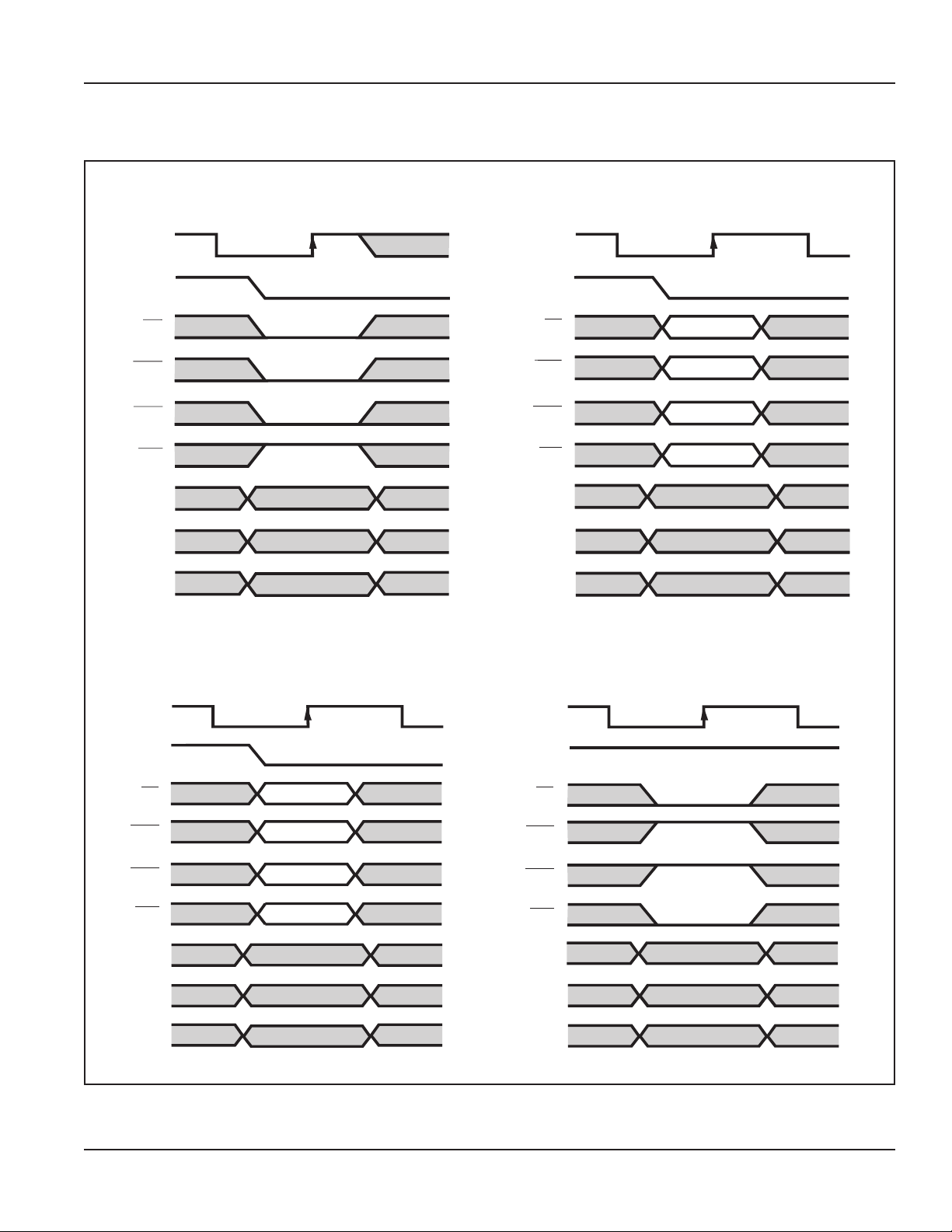
SIMPLIFIED STATE TRANSITION DIAGRAM (One Bank Operation)
SELF
REFRESH
SREF entry
SREF exit
®
WRIT
CKE_
MODE
REGISTER
MRS
IDLE
REF
SET
CKE_
CKE
ACT
CKE_
CKE
READ
BANK
ACTIVE
READ
READA
BST BST
WRIT
WRITA
WRITE
WRIT
AUTO
REFRESH
IDLE
POWER
DOWN
ACTIVE
POWER
DOWN
READ
READ
CKE_
20
CLOCK
SUSPEND
POWER APPLIED
CKE
WRITA
CKE_
CKE
WRITE WITH
AUTO
PRECHARGE
POWER ON
Automatic transition following the
completion of command execution.
Transition due to command input.
WRITA
READA
READA
CKE_
READ WITH
CKE
CLOCK
SUSPEND
CKE
AUTO
PRECHARGE
PRE
PRE
PRE-
CHARGE
PRE
PRE
Integrated Silicon Solution, Inc. — www.issi.com —
1-800-379-4774
Rev. D
11/03/06

IS42S16100C1 ISSI
®
Device Initialization At Power-On
(Power-On Sequence)
As is the case with conventional DRAMs, the IS42S16100C1
product must be initialized by executing a stipulated poweron sequence after power is applied.
After power is applied and VDD and VDDQ reach their
stipulated voltages, set and hold the CKE and DQM pins
HIGH for 100 µs. Then, execute the precharge command to
precharge both bank. Next, execute the auto-refresh
command twice or more and define the device operation
mode by executing a mode register set command.
The mode register set command can be also set before
auto-refresh command.
Mode Register Settings
The mode register set command sets the mode register.
When this command is executed, pins A0 to A9, A10, and
A11 function as data input pins for setting the register, and
this data becomes the device internal OP code. This OP
code has four fields as listed in the table below.
Burst Length
When writing or reading, data can be input or output data
continuously. In these operations, an address is input only
once and that address is taken as the starting address
internally by the device. The device then automatically
generates the following address. The burst length field in
the mode register stipulates the number of data items input
or output in sequence. In the IS42S16100C1 product, a
burst length of 1, 2, 4, 8, or full page can be specified. See
the table on the next page for details on setting the mode
register.
Burst Type
The burst data order during a read or write operation is
stipulated by the burst type, which can be set by the mode
register set command. The IS42S16100C1 product supports
sequential mode and interleaved mode burst type settings.
See the table on the next page for details on setting the
mode register. See the “Burst Length and Column Address
Sequence” item for details on DQ data orders in these
modes.
Input Pin Field
A11, A10, A9, A8, A7 Mode Options
A6, A5, A4 CAS Latency
A3 Burst Type
A2, A1, A0 Burst Length
Note that the mode register set command can be executed
only when both banks are in the idle (inactive) state. Wait
at least two cycles after executing a mode register set
command before executing the next command.
CASCAS
CAS Latency
CASCAS
During a read operation, the between the execution of the
read command and data output is stipulated as the CAS
latency. This period can be set using the mode register set
command. The optimal CAS latency is determined by the
clock frequency and device speed grade. See the “Operating
Frequency / Latency Relationships” item for details on the
relationship between the clock frequency and the CAS
latency. See the table on the next page for details on setting
the mode register.
Write Mode
Burst write or single write mode is selected by the OP code
(A11, A10, A9) of the mode register.
A burst write operation is enabled by setting the OP code
(A11, A10, A9) to (0,0,0). A burst write starts on the same
cycle as a write command set. The write start address is
specified by the column address and bank select address
at the write command set cycle.
A single write operation is enabled by setting OP code
(A11, A10, A9) to (0, 0,1). In a single write operation, data
is only written to the column address and bank select
address specified by the write command set cycle without
regard to the bust length setting.
Integrated Silicon Solution, Inc. — www.issi.com —
Rev. D
11/03/06
1-800-379-4774
21

IS42S16100C1 ISSI
MODE REGISTER
A11 A10 A9 A8 A7 A6 A5 A4 A3 A2 A1 A0
WRITE MODE LT MODE BT BL
Burst Length 0 0 0 1 1
Address Bus (Ax)
Mode Register (Mx)
M2 M1 M0 Sequential Interleaved
001 2 2
010 4 4
011 8 8
1 0 0 Reserved Reserved
1 0 1 Reserved Reserved
1 1 0 Reserved Reserved
1 1 1 Full Page Reserved
®
Burst Type 0 Sequential
Latency Mode 0 0 0 Reserved
M11 M10 M9 M8 M7 Write Mode
00100 Burst Read & Single Write
00000 Burst Read & Burst Write
Note: Other values for these bits are reserved.
M3 Type
1 Interleaved
M6 M5 M4
0 0 1 Reserved
010 2
011 3
1 0 0 Reserved
1 0 1 Reserved
1 1 0 Reserved
1 1 1 Reserved
CASCAS
CAS Latency
CASCAS
22
Integrated Silicon Solution, Inc. — www.issi.com —
1-800-379-4774
Rev. D
11/03/06

IS42S16100C1 ISSI
BURST LENGTH AND COLUMN ADDRESS SEQUENCE
Column Address Address Sequence
Burst Length A2 A1 A0 Sequential Interleaved
2 X X 0 0-1 0-1
X X 1 1-0 1-0
4 X 0 0 0-1-2-3 0-1-2-3
X 0 1 1-2-3-0 1-0-3-2
X 1 0 2-3-0-1 2-3-0-1
X 1 1 3-0-1-2 3-2-1-0
8 0 0 0 0-1-2-3-4-5-6-7 0-1-2-3-4-5-6-7
0 0 1 1-2-3-4-5-6-7-0 1-0-3-2-5-4-7-6
0 1 0 2-3-4-5-6-7-0-1 2-3-0-1-6-7-4-5
0 1 1 3-4-5-6-7-0-1-2 3-2-1-0-7-6-5-4
1 0 0 4-5-6-7-0-1-2-3 4-5-6-7-0-1-2-3
1 0 1 5-6-7-0-1-2-3-4 5-4-7-6-1-0-3-2
1 1 0 6-7-0-1-2-3-4-5 6-7-4-5-2-3-0-1
1 1 1 7-0-1-2-3-4-5-6 7-6-5-4-3-2-1-0
®
Full Page n n n Cn, Cn+1, Cn+2 None
(256) Cn+3, Cn+4.....
...Cn-1(Cn+255),
Cn(Cn+256).....
Notes:
1. The burst length in full page mode is 256.
Integrated Silicon Solution, Inc. — www.issi.com —
Rev. D
11/03/06
1-800-379-4774
23

IS42S16100C1 ISSI
BANK SELECT AND PRECHARGE ADDRESS ALLOCATION
Row X0 — Row Address
X1 — Row Address
X2 — Row Address
X3 — Row Address
X4 — Row Address
X5 — Row Address
X6 — Row Address
X7 — Row Address
X8 — Row Address
X9 — Row Address
X10 0 Precharge of the Selected Bank (Precharge Command) Row Address
1 Precharge of Both Banks (Precharge Command) (Active Command)
X11 0 Bank 0 Selected (Precharge and Active Command)
1 Bank 1 Selected (Precharge and Active Command)
Column Y0 — Column Address
Y1 — Column Address
Y2 — Column Address
Y3 — Column Address
Y4 — Column Address
Y5 — Column Address
Y6 — Column Address
Y7 — Column Address
Y8 — Don’t Care
Y9 — Don’t Care
Y10 0 Auto-Precharge - Disabled
1 Auto-Precharge - Enables
Y11 0 Bank 0 Selected (Read and Write Commands)
1 Bank 1 Selected (Read and Write Commands)
®
24
Integrated Silicon Solution, Inc. — www.issi.com —
1-800-379-4774
Rev. D
11/03/06
IS42S16100C1 ISSI
Burst Read
The read cycle is started by executing the read command.
The address provided during read command execution is
used as the starting address. First, the data corresponding
to this address is output in synchronization with the clock
signal after the CAS latency period. Next, data corresponding
to an address generated automatically by the device is
output in synchronization with the clock signal.
The output buffers go to the LOW impedance state CAS
latency minus one cycle after the read command, and go
to the HIGH impedance state automatically after the last
data is output. However, the case where the burst length
CLK
is a full page is an exception. In this case the output
buffers must be set to the high impedance state by
executing a burst stop command.
Note that upper byte and lower byte output data can be
masked independently under control of the signals applied
to the U/LDQM pins. The delay period (tQMD) is fixed at two,
regardless of the CAS latency setting, when this function
is used.
The selected bank must be set to the active state before
executing this command.
®
COMMAND
UDQM
LDQM
DQ8-DQ15
DQ0-DQ 7
CAS latency = 3, burst length = 4
READ A0
t
QMD=2
D
READ (CA=A, BANK 0) DATA MASK (LOWER BYTE)
DATA MASK (UPPER BYTE)
Burst Write
The write cycle is started by executing the command. The
address provided during write command execution is used
as the starting address, and at the same time, data for this
address is input in synchronization with the clock signal.
Next, data is input in other in synchronization with the clock
signal. During this operation, data is written to address
generated automatically by the device. This cycle
terminates automatically after a number of clock cycles
determined by the stipulated burst length. However, the
case where the burst length is a full page is an exception.
In this case the write cycle must be terminated by executing
OUT
OUT
A0
A0
OUT
D
HI-Z
D
OUT
A2 D
OUT
A3
HI-Z
A1D
HI-Z
a burst stop command. The latency for DQ pin data input
is zero, regardless of the CAS latency setting. However, a
wait period (write recovery: tDPL) after the last data input is
required for the device to complete the write operation.
Note that the upper byte and lower byte input data can be
masked independently under control of the signals applied
to the U/LDQM pins. The delay period (tDMD) is fixed at zero,
regardless of the CAS latency setting, when this function
is used.
The selected bank must be set to the active state before
executing this command.
CLK
COMMAND
DQ
WRITE
DIN 0DIN 1DIN 2DIN 3
BURST LENGTH
CAS latency = 2,3, burst length = 4
Integrated Silicon Solution, Inc. — www.issi.com —
Rev. D
11/03/06
1-800-379-4774
25

IS42S16100C1 ISSI
Read With Auto-Precharge
The read with auto-precharge command first executes a
burst read operation and then puts the selected bank in the
precharged state automatically. After the precharge completes, the bank goes to the idle state. Thus this command
performs a read command and a precharge command in a
single operation.
During this operation, the delay period (tPQL) between the
last burst data output and the start of the precharge
operation differs depending on the CAS latency setting.
three, the precharge operation starts on two clock cycles
before the last burst data is output (tPQL = –2). Therefore,
the selected bank can be made active after a delay of tRP
from the start position of this precharge operation.
The selected bank must be set to the active state before
executing this command.
The auto-precharge function is invalid if the burst length is
set to full page.
®
When the CAS latency setting is two, the precharge
operation starts on one clock cycle before the last burst
data is output (tPQL = –1). When the CAS latency setting is
CLK
COMMAND
DQ
READ WITH AUTO-PRECHARGE
CAS latency = 2, burstlength = 4
READA 0
(BANK 0)
D
OUT
0D
PRECHARGE START
OUT
CASCAS
CAS Latency 3 2
CASCAS
1D
OUT
tPQL –2 –1
ACT 0
t
PQL
2D
OUT
3
t
RP
CLK
COMMAND
READA 0
DQ
READ WITH AUTO-PRECHARGE
(BANK 0)
CAS latency = 3, burstlength = 4
26
t
PQL
D
OUT
0D
OUT
1D
OUT
2D
OUT
3
t
PRECHARGE START
RP
Integrated Silicon Solution, Inc. — www.issi.com —
ACT 0
1-800-379-4774
Rev. D
11/03/06

IS42S16100C1 ISSI
Write With Auto-Precharge
The write with auto-precharge command first executes a
burst write operation and then puts the selected bank in the
precharged state automatically. After the precharge
completes the bank goes to the idle state. Thus this
command performs a write command and a precharge
command in a single operation.
During this operation, the delay period (t
DAL) between the
last burst data input and the completion of the precharge
operation differs depending on the CAS latency setting.
The delay (tDAL) is tRP plus one CLK period. That is, the
precharge operation starts one clock period after the last
burst data input.
Therefore, the selected bank can be made active after a
delay of tDAL.
The selected bank must be set to the active state before
executing this command.
The auto-precharge function is invalid if the burst length is
set to full page.
CASCAS
CAS Latency 3 2
CASCAS
t
DAL 1CLK 1CLK
+tRP +tRP
®
CLK
COMMAND
DQ
WRITE WITH AUTO-PRECHARGE
CAS latency = 2, burstlength = 4
WRITE A0
DIN 0DIN 1DIN 2DIN 3
(BANK 0)
CLK
COMMAND
DQ
WRITE WITH AUTO-PRECHARGE
WRITE A0
DIN 0DIN 1DIN 2DIN 3
(BANK 0)
ACT 0
PRECHARGE START
tRP
tDAL
ACT 0
PRECHARGE START
tRP
tDAL
CAS latency = 3, burstlength = 4
Integrated Silicon Solution, Inc. — www.issi.com —
Rev. D
11/03/06
1-800-379-4774
27

IS42S16100C1 ISSI
Interval Between Read Command
A new command can be executed while a read cycle is in
progress, i.e., before that cycle completes. When the
second read command is executed, after the CAS latency
has elapsed, data corresponding to the new read command
is output in place of the data due to the previous read
command.
CLK
The interval between two read command (tCCD) must be at
least one clock cycle.
The selected bank must be set to the active state before
executing this command.
®
COMMAND
DQ
READ A0 READ B0
DOUT A0 DOUT B0 DOUT B1
tCCD
READ (CA=A, BANK 0) READ (CA=B, BANK 0)
CAS latency = 2, burstlength = 4
Interval Between Write Command
A new command can be executed while a write cycle is in
progress, i.e., before that cycle completes. At the point the
second write command is executed, data corresponding to
the new write command can be input in place of the data
for the previous write command.
CLK
OUT B2
D
DOUT B3
The interval between two write commands (tCCD) must be
at least one clock cycle.
The selected bank must be set to the active state before
executing this command.
COMMAND
DQ
WRITE (CA=A, BANK 0) WRITE (CA=B, BANK 0)
CAS latency = 3, burstlength = 4
28
t
CCD
WRITE A0 WRITE B0
DIN A0 DIN B0 DIN B1 DIN B2 DIN B3
Integrated Silicon Solution, Inc. — www.issi.com —
1-800-379-4774
Rev. D
11/03/06

IS42S16100C1 ISSI
)
Interval Between Write and Read Commands
A new read command can be executed while a write cycle
is in progress, i.e., before that cycle completes. Data
corresponding to the new read command is output after the
CAS latency has elapsed from the point the new read
command was executed. The I/On pins must be placed in
the HIGH impedance state at least one cycle before data
is output during this operation.
CLK
t
CCD
The interval (tCCD) between command must be at least one
clock cycle.
The selected bank must be set to the active state before
executing this command.
®
COMMAND
DQ
CAS latency = 2, burstlength = 4
WRITE A0 READ B0
DIN A0
WRITE (CA=A, BANK 0) READ (CA=B, BANK 0)
CLK
COMMAND
DQ
WRITE A0 READ B0
DIN A0 D
t
CCD
HI-Z
D
OUT
B0 D
HI-Z
OUT
B1 D
OUT
B0 D
OUT
OUT
B2D
B1 D
OUT
OUT
B3
B2D
OUT
B3
WRITE (CA=A, BANK 0)READ (CA=B, BANK 0
CAS latency = 3, burstlength = 4
Integrated Silicon Solution, Inc. — www.issi.com —
Rev. D
11/03/06
1-800-379-4774
29

IS42S16100C1 ISSI
Interval Between Read and Write Commands
®
A read command can be interrupted and a new write
command executed while the read cycle is in progress,
i.e., before that cycle completes. Data corresponding to
the new write command can be input at the point new
write command is executed. To prevent collision
between input and output data at the DQn pins during
this operation, the
CLK
t
CCD
COMMAND
READ A0
WRITE B0
U/LDQM
DQ
HI-Z
READ (CA=A, BANK 0) WRITE (CA=B, BANK 0)
DIN B0 DIN B2DIN B1 DIN B3
output data must be masked using the U/LDQM pins. The
interval (t
CCD) between these commands must be at least
one clock cycle.
The selected bank must be set to the active state before
executing this command.
CAS latency = 2, 3, burstlength = 4
30
Integrated Silicon Solution, Inc. — www.issi.com —
1-800-379-4774
Rev. D
11/03/06

IS42S16100C1 ISSI
)
)
®
Precharge
The precharge command sets the bank selected by pin A11
to the precharged state. This command can be executed at
a time tRAS following the execution of an active command to
the same bank. The selected bank goes to the idle state at
a time tRP following the execution of the precharge command,
and an active command can be executed again for that
bank.
If pin A10 is low when this command is executed, the bank
selected by pin A11 will be precharged, and if pin A10 is
HIGH, both banks will be precharged at the same time. This
input to pin A11 is ignored in the latter case.
CLK
COMMAND
READ A0
Read Cycle Interruption
Using the Precharge Command
A read cycle can be interrupted by the execution of the
precharge command before that cycle completes. The
delay time (tRQL) from the execution of the precharge
command to the completion of the burst output is the
clock cycle of CAS latency.
CASCAS
CAS Latency 3 2
CASCAS
tRQL 32
t
RQL
PRE 0
DQ
READ (CA=A, BANK 0) PRECHARGE (BANK 0)
CAS latency = 2, burstlength = 4
CLK
COMMAND
READ A0
DQ
READ (CA=A, BANK 0
CAS latency = 3, burstlength = 4
DOUT A0 DOUT A1 DOUT A2
t
RQL
PRE 0
DOUT A0 DOUT A1 DOUT A2
PRECHARGE (BANK 0
HI-Z
HI-Z
Integrated Silicon Solution, Inc. — www.issi.com —
Rev. D
11/03/06
1-800-379-4774
31

IS42S16100C1 ISSI
Write Cycle Interruption Using the
Precharge Command
A write cycle can be interrupted by the execution of the
precharge command before that cycle completes. The
delay time (tWDL) from the precharge command to the point
where burst input is invalid, i.e., the point where input data
is no longer written to device internal memory is zero clock
cycles regardless of the CAS.
To inhibit invalid write, the DQM signal must be asserted
HIGH with the precharge command.
This precharge command and burst write command must
be of the same bank, otherwise it is not precharge interrupt
but only another bank precharge of dual bank operation.
Inversely, to write all the burst data to the device, the
precharge command must be executed after the write
data recovery period (t
precharge command must be executed on one clock
cycle that follows the input of the last burst data item.
CASCAS
CAS Latency 3 2
CASCAS
tWDL 00
tDPL 11
DPL) has elapsed. Therefore, the
CLK
®
COMMAND
DQM
DQ
WRITE (CA=A, BANK 0)
CAS latency = 2, burstlength = 4
CLK
COMMAND
WRITE A0
WRITE A0
DIN A0
IN
A1 DIN A2 DIN A3
D
PRECHARGE (BANK 0)
DPL
t
t
WDL
PRE 0
MASKED BY DQM
PRE 0
=0
DQ
CAS latency = 3, burstlength = 4
32
DIN A0
WRITE (CA=A, BANK 0) PRECHARGE (BANK 0)
IN
A1 DIN A2 DIN A3
D
Integrated Silicon Solution, Inc. — www.issi.com —
1-800-379-4774
Rev. D
11/03/06

IS42S16100C1 ISSI
Read Cycle (Full Page) Interruption Using
the Burst Stop Command
The IS42S16100C1 can output data continuously from the
burst start address (a) to location a+255 during a read cycle
in which the burst length is set to full page. The
IS42S16100C1 repeats the operation starting at the 256th
cycle with the data output returning to location (a) and
continuing with a+1, a+2, a+3, etc. A burst stop command
must be executed to terminate this cycle. A precharge
command must be executed within the ACT to PRE
command period (tRAS max.) following the burst stop
command.
CLK
After the period (t
stop following the execution of the burst stop command
has elapsed, the outputs go to the HIGH impedance
state. This period (tRBD) is two clock cycle when the
CAS latency is two and three clock cycle when the CAS
latency is three.
CASCAS
CAS Latency 3 2
CASCAS
RBD) required for burst data output to
tRBD 32
®
COMMAND
READ A0
DQ
READ (CA=A, BANK 0)
CAS latency = 2, burstlength = 4
CLK
COMMAND
READ A0
DQ
D
OUT
A0 D
OUT
D
OUT
A0 D
A0 D
OUT
OUT
A1 D
BURST STOP
A0
OUT
BST
D
OUT
BST
A2 D
A1
t
RBD
D
OUT
OUT
A3
t
RBD
A2
D
HI-Z
OUT
A3
HI-Z
READ (CA=A, BANK 0) BURST STOP
CAS latency = 3, burstlength = 4
Integrated Silicon Solution, Inc. — www.issi.com —
Rev. D
11/03/06
1-800-379-4774
33

IS42S16100C1 ISSI
Write Cycle (Full Page) Interruption Using
the Burst Stop Command
The IS42S16100C1 can input data continuously from
the burst start address (a) to location a+255 during a
write cycle in which the burst length is set to full page.
The IS42S16100C1 repeats the operation starting at the
256th cycle with data input returning to location (a) and
continuing with a+1, a+2, a+3, etc. A burst stop
command must be executed to terminate this cycle. A
precharge command
CLK
COMMAND
WRITE A0
must be executed within the ACT to PRE command
period (tRAS max.) following the burst stop command.
After the period (tWBD) required for burst data input to
stop following the execution of the burst stop command
has elapsed, the write cycle terminates. This period
(tWBD) is zero clock cycles, regardless of the CAS
latency.
t
WBD=0
BST PRE 0
INVALID DATA
tRP
®
DQ
DIN A0 DIN A1 DIN ADIN A1 DIN A2
READ (CA=A, BANK 0) BURST STOP
Burst Data Interruption Using the U/LDQM
Pins (Read Cycle)
Burst data output can be temporarily interrupted (masked)
during a read cycle using the U/LDQM pins. Regardless of
the CAS latency, two clock cycles (tQMD) after one of the U/
LDQM pins goes HIGH, the corresponding outputs go to the
HIGH impedance state. Subsequently, the outputs are
maintained in the high impedance state as long as that U/
LDQM pin remains HIGH. When the U/LDQM pin goes
LOW, output is resumed at a time tQMD later. This output
CLK
COMMAND
UDQM
READ A0
t
QMD=2
PRECHARGE (BANK 0)
Don't Care
control operates independently on a byte basis with the
UDQM pin controlling upper byte output (pins
DQ8-DQ15) and the LDQM pin controlling lower byte output
(pins DQ0 to DQ7).
Since the U/LDQM pins control the device output buffers
only, the read cycle continues internally and, in particular,
incrementing of the internal burst counter continues.
LDQM
DQ8-DQ15
DQ0-DQ 7
CAS latency = 2, burstlength = 4
34
D
OUT
A0
OUT
A0
READ (CA=A, BANK 0) DATA MASK (LOWER BYTE)
DATA MASK (UPPER BYTE)
HI-Z
OUT
A1D
D
Integrated Silicon Solution, Inc. — www.issi.com —
D
OUT
HI-Z
A2 D
OUT
A3
HI-Z
1-800-379-4774
Rev. D
11/03/06

IS42S16100C1 ISSI
Burst Data Interruption U/LDQM Pins (Write
Cycle)
Burst data input can be temporarily interrupted (muted )
during a write cycle using the U/LDQM pins. Regardless of
the CAS latency, as soon as one of the U/LDQM pins goes
HIGH, the corresponding externally applied input data will
no longer be written to the device internal circuits.
Subsequently, the corresponding input continues to be
muted as long as that U/LDQM pin remains HIGH.
The IS42S16100C1 will revert to accepting input as soon
as
CLK
that pin is dropped to LOW and data will be written to the
device. This input control operates independently on a byte
basis with the UDQM pin controlling upper byte input (pin
DQ8 to DQ15) and the LDQM pin controlling the lower byte
input (pins DQ0 to DQ7).
Since the U/LDQM pins control the device input buffers
only, the cycle continues internally and, in particular,
incrementing of the internal burst counter continues.
®
COMMAND
UDQM
LDQM
DQ8-DQ15
DQ0-DQ7
WRITE (CA=A, BANK 0) DATA MASK (LOWER BYTE)
DATA MASK (UPPER BYTE)
WRITE A0
t
DMD=0
D
IN
A0 DIN A3
CAS latency = 2, burstlength = 4
Burst Read and Single Write
The burst read and single write mode is set up using the
mode register set command. During this operation, the
burst read cycle operates normally, but the write cycle only
writes a single data item for each write cycle. The CAS
latency and DQM latency are the same as in normal mode.
DIN A1
DIN A2
D
IN
A3
Don't Care
CLK
COMMAND
DQ
CAS latency = 2, 3
Integrated Silicon Solution, Inc. — www.issi.com —
Rev. D
11/03/06
WRITE A0
DIN A0
WRITE (CA=A, BANK 0)
1-800-379-4774
35

IS42S16100C1 ISSI
Bank Active Command Interval
When the selected bank is precharged, the period trp
has elapsed and the bank has entered the idle state, the
bank can be activated by executing the active
command. If the other bank is in the idle state at that
time, the active command can be executed for that bank
after the period tRRD has elapsed. At that point both
banks will be in the active state. When a bank active
command has been executed, a precharge command
must be executed for
CLK
t
RRD
COMMAND
BANK ACTIVE (BANK 0) BANK ACTIVE (BANK 1)
ACT 0 ACT 1
that bank within the ACT to PRE command period (tRAS
max). Also note that a precharge command cannot be
executed for an active bank before tRAS (min) has elapsed.
After a bank active command has been executed and the
trcd period has elapsed, read write (including auto-precharge)
commands can be executed for that bank.
®
CLK
t
RCD
COMMAND
BANK ACTIVE (BANK 0) BANK ACTIVE (BANK 0)
ACT 0 READ 0
CAS latency = 3
Clock Suspend
When the CKE pin is dropped from HIGH to LOW during a
read or write cycle, the IS42S16100C1 enters clock
suspend mode on the next CLK rising edge. This command
reduces the device power dissipation by stopping the
device internal clock. Clock suspend mode continues as
long as the CKE pin remains low. In this state, all inputs
other than CKE pin are invalid and no other commands can
be executed. Also, the device internal states are maintained.
When the CKE pin goes from LOW to HIGH clock suspend
mode is terminated on the next CLK rising edge and device
operation resumes.
CLK
The next command cannot be executed until the recovery
period (tCKA) has elapsed.
Since this command differs from the self-refresh command
described previously in that the refresh operation is not
performed automatically internally, the refresh operation
must be performed within the refresh period (tref). Thus the
maximum time that clock suspend mode can be held is just
under the refresh cycle time.
CKE
COMMAND
DQ
CAS latency = 2, burstlength = 4
36
READ 0
D
OUT
0D
READ (BANK 0) CLOCK SUSPEND
Integrated Silicon Solution, Inc. — www.issi.com —
OUT
1D
OUT
2D
OUT
3
1-800-379-4774
Rev. D
11/03/06

IS42S16100C1 ISSI
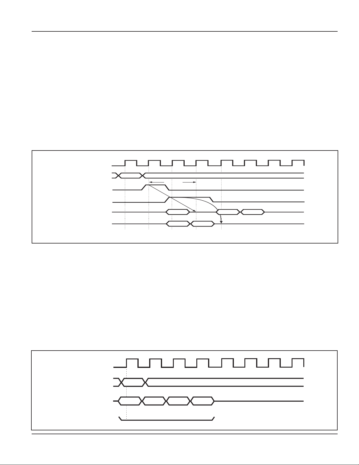
OPERATION TIMING EXAMPLE
Power-On Sequence, Mode Register Set Cycle
T0 T1 T2 T3 T10 T17 T18 T19 T20
CLK
t
CHI
t
CKE
CS
RAS
HIGH
t
CS
t
CS
t
CS
CK
t
CH
t
t
CH
CH
t
CL
®
CAS
WE
A0-A9
A10
A11
DQM
DQ
HIGH
t
CS
t
AS
BANK 0 & 1
WAIT TIME
T=100 µs
<
PALL
t
CH
t
AH
t
t
RP
><
REF
>
RC
REF
t
RC
>
t
AS
t
t
AS
AS
CODE
CODE
CODE
MRS
><
t
AH
t
AH
t
AH
t
MCD
ROW
ROW
BANK 1
BANK 0
<
ACT
><
t
RAS
t
RC
CAS latency = 2, 3
Integrated Silicon Solution, Inc. — www.issi.com —
Rev. D
11/03/06
1-800-379-4774
Undefined
Don't Care
37

IS42S16100C1 ISSI
Power-Down Mode Cycle
T0 T1 T2 T3 Tn Tn+1 Tn+2 Tn+3
CLK
t
CKE
CS
RAS
CAS
WE
A0-A9
A10
A11
t
CKS
t
CS
t
CK
t
CKA
t
CH
t
CS
t
CS
t
CS
t
AS
BANK 0 OR 1
CHI
t
CH
t
CH
t
CH
t
AH
BANK 0 & 1
BANK 1
BANK 0
t
CL
t
CKS
t
CKH
t
CKA
t
AS
t
AH
ROW
ROW
BANK 1
BANK 0
®
DQM
DQ
CAS latency = 2, 3
PRE
<
<
PALL
EXIT
t
t
RP
SBY
>
>
POWER DOWN MODE
POWER DOWN MODE
<
ACT
RAS
t
RC
><
>
Undefined
Don't Care
38
Integrated Silicon Solution, Inc. — www.issi.com —
1-800-379-4774
Rev. D
11/03/06

IS42S16100C1 ISSI
Auto-Refresh Cycle
T0 T1 T2 T3 Tl Tm Tn Tn+1
CLK
t
CHI
t
t
t
t
CK
t
CH
CS
CS
CS
t
t
t
CH
CH
CH
t
CL
CKE
CS
RAS
CAS
WE
t
CKS
t
CS
®
A0-A9
t
A10
A11
DQM
DQ
CAS latency = 2, 3
t
AS
AH
BANK 0 & 1
t
t
RP
<
PALL
><
REF
>
RC
ROW
ROW
BANK 1
BANK 0
t
t
RC
REF
><
REF
>
RC
<
ACT
t
><
Undefined
Don't Care
RAS
t
RC
Integrated Silicon Solution, Inc. — www.issi.com —
Rev. D
11/03/06
1-800-379-4774
39

IS42S16100C1 ISSI
Self-Refresh Cycle
T0 T1 T2 T3 Tm Tm+2Tm+1 Tn
CLK
t
CKE
CS
RAS
CAS
WE
t
CKS
t
CS
t
CKA
t
t
t
t
CK
t
CH
CS
CS
CS
CHI
t
CH
t
CH
t
CH
t
CL
t
CKS
t
CKS
t
CKA
®
A0-A9
t
AS
A10
BANK 0 & 1
A11
DQM
DQ
PALL
><
<
CAS latency = 2, 3
Note 1: A8,A9 = Don’t Care.
t
AH
t
RP
SELF
>
SELF REFRESH MODE
EXIT
SELF
REFRESH
t
RC
t
<
REF
>
Undefined
Don't Care
RC
40
Integrated Silicon Solution, Inc. — www.issi.com —
1-800-379-4774
Rev. D
11/03/06

IS42S16100C1 ISSI
Read Cycle
T0 T1 T2 T3 T4 T5 T6 T7 T8 T9 T10
CLK
t
t
CK
t
CKA
t
CH
CS
CS
CS
CHI
t
CH
t
CH
t
CH
t
CL
CKE
CS
RAS
CAS
t
CKS
t
CS
t
t
t
®
WE
A0-A9
A10
A11
DQM
DQ
t
t
t
t
AS
AS
AS
AH
ROW ROW
t
AH
ROW
t
AH
BANK 1
t
CS
t
RCD
t
RAS
t
RC
<
ACT
><
READ
>
(1)
COLUMN m
BANK 0 AND 1
NO PRE
BANK 1 BANK 1
BANK 0 OR 1
BANK 1
BANK 0BANK 0
t
QMD
t
t
t
CAC
AC
LZ
t
AC
t
OH
D
OUT
mD
OUT
t
t
OH
m+1
t
CH
AC
BANK 0
t
OH
D
OUT
m+2
<
PRE
>
PALL
>
<
t
AC
t
RQL
t
RP
D
OUT
t
OH
m+3
t
HZ
ROW
BANK 0
t
RCD
t
RAS
t
RC
ACT
>
<
CAS latency = 2, burstlength = 4
Note 1: A8,A9 = Don’t Care.
Integrated Silicon Solution, Inc. — www.issi.com —
Rev. D
11/03/06
1-800-379-4774
Undefined
Don't Care
41

IS42S16100C1 ISSI
Read Cycle / Auto-Precharge
T0 T1 T2 T3 T4 T5 T6 T7 T8 T9 T10
CLK
tCKS
CKE
CS
RAS
CAS
tCK
tCKA
tCHtCS
tCHI
tCL
tCHtCS
tCHtCS
tCHtCS
®
WE
A0-A9
A10
A11
DQM
DQ
tAHtAS
ROW ROW
tAS
tAH
ROW
tAS
tAH
(1)
COLUMN m
AUTO PRE
BANK 1 BANK 1
BANK 1
tCS
BANK 0BANK 0
tQMD
tAC
tAC
tOH
D
OUT
mD
tCH
tAC tAC
tOH
OUT
m+1
D
OUT
tOH
m+2
D
OUT
tLZ
tRCD tCAC
tRAS
tPQL
tRP
tRC
<ACT><READA>
tOH
m+3
tHZ
ROW
BANK 0
tRCD
tRAS
tRC
<
ACT>
CAS latency = 2, burstlength = 4
Note 1: A8,A9 = Don’t Care.
42
Undefined
Don't Care
Integrated Silicon Solution, Inc. — www.issi.com —
1-800-379-4774
Rev. D
11/03/06

IS42S16100C1 ISSI
Read Cycle / Full Page
T0 T1 T2 T3 T4 T5 T6 T260 T261 T262 T263
CLK
t
t
CK
t
CKA
t
CH
CS
CS
CS
AS
AS
AS
CHI
t
CH
t
CH
t
CH
t
AH
ROW
t
AH
ROW
t
AH
BANK 0
t
RCD
t
RAS
t
RC
(BANK 0)
<
ACT 0
><
t
CL
READ0
t
CS
>
(1)
COLUMN
NO PRE
BANK 0
t
QMD
t
CAC
(BANK 0)
BANK 0 OR 1
BANK 0
t
CH
t
AC
t
LZ
t
AC
t
OH
D
OUT
0m D
OUT
t
AC
t
OH
0m+1
t
D
OUT
0m-1
OH
t
AC
t
OH
D
OUT
0m D
t
AC
t
RBD
<
OUT
BST
t
OH
0m+1
t
HZ
t
RP
(BANK 0)
><
PRE 0
>
CKE
CS
RAS
CAS
WE
A0-A9
A10
A11
DQM
DQ
t
CKS
t
CS
t
t
t
t
t
t
®
CAS latency = 2, burstlength = full page
Note 1: A8,A9 = Don’t Care.
Integrated Silicon Solution, Inc. — www.issi.com —
Rev. D
11/03/06
1-800-379-4774
Undefined
Don't Care
43

IS42S16100C1 ISSI
Read Cycle / Ping-Pong Operation (Bank Switching)
T0 T1 T2 T3 T4 T5 T6 T7 T8 T9 T10
CLK
t
CHI
t
CK
CKA
t
CH
t
CL
t
CH
t
CH
t
CH
t
AH
ROW
t
AH
ROW
t
AS
AH
BANK 0 BANK 0
t
CS
t
RRD
(BANK 0 TO 1)
t
RCD
(BANK 0)
t
RAS
(BANK 0)
t
RC
(BANK 0)
<
ACT 0
><
(1)(1)
COLUMN COLUMN
ROW
AUTO PRE AUTO PRE
ROW
NO PRE
BANK 1
t
QMD
t
AC
D
OUT
t
LZ
t
CAC
(BANK 1)
READ 0
<
<
READA 0
ACT1
>
><
t
RCD
(BANK 1)
>
t
AC
t
OH
0m D
t
RAS
(BANK 1)
t
RC
(BANK 1)
READ 1
<
READA 1
BANK 1
BANK 0 OR 1 BANK 0 OR 1NO PRE
BANK 0
t
AC
t
OH
OUT
0m+1 D
t
t
HZ
t
CAC
(BANK 1)
><
>
LZ
t
RP
(BANK 0)
PRE 0
><
ROW
ROW
BANK 0
t
CH
t
AC
t
OH
OUT
1m D
<
ACT 0
OUT
t
OH
1m+1
t
HZ
t
RCD
(BANK 0)
t
RAS
(BANK 0)
t
RC
(BANK 0)
>
BANK 1
PRE 1
>
t
RP
(BANK1)
CKE
CS
RAS
CAS
WE
A0-A9
A10
A11
DQM
DQ
t
CKS
t
CS
t
CS
t
CS
t
CS
t
AS
t
AS
t
t
®
CAS latency = 2, burstlength = 2
Note 1: A8,A9 = Don’t Care.
44
Undefined
Don't Care
Integrated Silicon Solution, Inc. — www.issi.com —
1-800-379-4774
Rev. D
11/03/06

IS42S16100C1 ISSI
Write Cycle
T0 T1 T2 T3 T4 T5 T7 T6 T8 T9 T10
CLK
t
CHI
CK
CKA
CH
ROW ROW
AS
ROW
BANK 1
BANK 0
t
CL
t
CH
t
CH
t
CH
t
AH
(1)
COLUMN m
t
AH
BANK 0 AND 1
NO PRE
t
AH
BANK 1
BANK 0 OR 1
BANK 1
t
CS
BANK 0
BANK 0
t
CH
ROW
BANK 1
BANK 0
CKE
CS
RAS
CAS
WE
A0-A9
A10
A11
DQM
t
CKS
t
CS
t
t
t
CS
t
CS
t
CS
t
AS
t
t
t
AS
®
t
DQ
DS
t
RCD
t
RAS
t
RC
ACT
><
DIN m
WRIT
t
>
DH
t
DS
t
DH
IN m+1
D
CAS latency = 2, burstlength = 4
Note 1: A8,A9 = Don’t Care.
Integrated Silicon Solution, Inc. — www.issi.com —
Rev. D
11/03/06
t
DH
t
D
IN m+2
DS
t
DS
1-800-379-4774
t
DH
D
IN m+3
t
DPL
<
PRE
<
PALL
t
RCD
t
RP
>
ACT
<
><
t
RAS
t
RC
>
Undefined
Don't Care
45

IS42S16100C1 ISSI
Write Cycle / Auto-Precharge
T0 T1 T2 T3 T4 T5 T7 T6 T8 T9 T10
CLK
tCKS
CKE
CS
RAS
CAS
WE
A0-A9
tCHI
tCK
tCKA
tCHtCS
ROW ROW
tCL
tCHtCS
tCHtCS
tCHtCS
tAHtAS
(1)
COLUMN m
®
tAS
A10
A11
ROW
tAS
BANK 1
BANK 0
DQM
DQ
CAS latency = 2, burstlength = 4
Note 1: A8,A9 = Don’t Care.
tAH
tAH
tRCD
tRAS
tRC
AUTO PRE
BANK 1
BANK 0
tCS
tDS tDS tDS
tDH
DIN m
D
IN
tDH
m+1
D
tDH
IN
m+2
tDS
ROW
BANK 1
tCH
tDH
D
IN
m+3
tDAL tRCD
tRP
BANK 0
<ACT><ACT><WRITA>
tRAS
tRC
Undefined
Don't Care
46
Integrated Silicon Solution, Inc. — www.issi.com —
1-800-379-4774
Rev. D
11/03/06

IS42S16100C1 ISSI
Write Cycle / Full Page
T0 T1 T2 T3 T4 T5 T259T258 T260 T261 T262
CLK
tCKS
CKE
CS
RAS
CAS
WE
A0-A9
A10
A11
tCK
tCKA
tCHtCS
tAS
tAS
tCHI
tCHtCS
tCHtCS
tCHtCS
tAHtAS
ROW
tAH
ROW
tAH
BANK 0
tCL
(1)
COLUMN m
NO PRE
BANK 0
BANK 0 OR 1
BANK 0
®
tCS
DQM
tDS tDS tDS
DQ
tRCD
tRAS
tRC
<ACT 0><WRIT0>
CAS latency = 2, burst length = full page
Note 1: A8,A9 = Don’t Care.
tDH tDH
DIN 0m
DIN 0m+1
D
IN
tDH
0m+2
tDS
tDH
D
IN
0m-1 D
IN
0m
tCH
tDPL
tRP
BST><PRE 0>
<
Undefined
Don't Care
Integrated Silicon Solution, Inc. — www.issi.com —
Rev. D
11/03/06
1-800-379-4774
47

IS42S16100C1 ISSI
Write Cycle / Ping-Pong Operation
T0 T1 T2 T3 T4 T5 T6 T7 T8 T9 T10
CLK
t
t
CK
t
CKA
t
CH
CS
CS
CS
AS
AS
AS
CHI
ROW
t
ROW
t
BANK 0
t
t
t
t
CH
CH
CH
AH
AH
AH
t
CL
(1) (1)
COLUMN COLUMN
ROW
AUTO PRE
ROW
NO PRE
t
CS
BANK 0
BANK 1
AUTO PRE
BANK 1
ROW
ROW
BANK 0 OR 1NO PRE
BANK 0 BANK 0
t
CH
CKE
CS
RAS
CAS
WE
A0-A9
A10
A11
DQM
t
CKS
t
CS
t
t
t
t
t
t
®
DQ
t
RRD
(BANK 0 TO 1)
t
RCD
(BANK 0)
t
RAS
(BANK 0)
t
RC
(BANK 0)
<
ACT 0
><
CAS latency = 2, burst length = 2
Note 1: A8,A9 = Don’t Care.
t
DS
t
DS
t
DH
DIN 0m
WRIT 0
>
<
WRITA 0
><
<
t
t
DH
DS
t
DH
t
DS
t
DH
t
DS
t
DH
t
DS
t
DH
t
DS
t
DS
t
DH
t
DH
DIN 0m+1 DIN 0m+2 DIN 0m+3 DIN 1m DIN 1m+1 DIN 1m+2 DIN 1m+3
t
DPL
t
RCD
ACT 1
(BANK 1)
t
RAS
(BANK 1)
t
RC
(BANK 1)
>
<
WRIT 1
><
WRITA 1
>
t
RP
(BANK 0)
PRE 0
><
ACT 0
(BANK 0)
(BANK 0)
(BANK 0)
>
t
DPL
t
RCD
t
RAS
t
RC
Undefined
Don't Care
48
Integrated Silicon Solution, Inc. — www.issi.com —
1-800-379-4774
Rev. D
11/03/06

IS42S16100C1 ISSI
Read Cycle / Page Mode
T0 T1 T2 T3 T4 T5 T6 T7 T8 T9 T10
CLK
t
CHI
t
CK
CKA
CH
ROW
ROW
t
t
t
t
t
t
AH
AH
CH
CH
CH
AH
t
CL
(1)
COLUMN m
NO PRE NO PRE
BANK 1
BANK 1
BANK 0
t
CS
BANK 0
t
QMD
t
t
LZ
t
RCD
t
RAS
t
RC
<
ACT
><
READ
t
CAC
>
(1)
COLUMN n
BANK 1
BANK 0
AC
t
AC
t
OH
DOUT mDOUT m+1 DOUT nDOUT n+1 DOUT oDOUT o+1
t
CAC
READ
>
t
OH
t
AC
(1)
COLUMN o
AUTO PRE
NO PRE
BANK 1
BANK 0
t
AC
t
OH
t
CAC
READ
><
<
<
READA
>
BANK 0 AND 1
BANK 0 OR 1
BANK 1
BANK 0
t
CH
t
AC
t
OH
PRE
>
<
<
PALL
>
t
OH
t
t
t
AC
RQL
RP
t
OH
t
HZ
CKE
CS
RAS
CAS
WE
A0-A9
A10
A11
DQM
DQ
t
CKS
t
CS
t
t
t
t
t
t
t
t
CS
CS
CS
AS
AS
AS
®
CAS latency = 2, burst length = 2
Note 1: A8,A9 = Don’t Care.
Integrated Silicon Solution, Inc. — www.issi.com —
Rev. D
11/03/06
1-800-379-4774
Undefined
Don't Care
49

IS42S16100C1 ISSI
Read Cycle / Page Mode; Data Masking
T0 T1 T2 T3 T4 T5 T6 T7 T8 T9 T10
CLK
tCKS
CKE
CS
RAS
CAS
WE
A0-A9
A10
A11
DQM
DQ
tCHI
tCK
tCL
tCKA
tCHtCS
tCHtCS
tCHtCS
tCHtCS
tAHtAS
ROW
tAS
tAH
ROW
tAS
tAH
BANK 1
BANK 0
tRCD tCAC tCAC tCAC tRQL
tRAS
tRC
<ACT><READ>
(1) (1)
COLUMN m
NO PRE NO PRE
BANK 1
tCS
tQMD
tAC
tLZ
COLUMN n
COLUMN o
AUTO PRE
BANK 1
NO PRE
NO PRE
BANK 1
BANK 0
tCH
tAC
tOH
D
OUT
mD
BANK 0
tAC tAC tAC
tOH tOH tOH
OUT
m+1 D
tHZ
READ, ENB><MASK>
<
<
READA, ENB>
(1)
BANK 0 AND 1
BANK 0 OR 1
BANK 1
tQMD
BANK 0 BANK 0
tOH
OUT
nD
tLZ
OUT
oD
OUT
o+1
tHZ
tRP
PRE>
<
<
PALL>
®
CAS latency = 2, burst length = 2
Note 1: A8,A9 = Don’t Care.
50
Integrated Silicon Solution, Inc. — www.issi.com —
Undefined
Don't Care
1-800-379-4774
Rev. D
11/03/06

IS42S16100C1 ISSI
Write Cycle / Page Mode
T0 T1 T2 T3 T4 T5 T6 T7 T8 T9 T10
CLK
t
t
CK
t
CKA
t
CH
CS
CS
CS
AS
AS
AS
CHI
ROW
t
ROW
t
BANK 1
BANK 0
t
t
t
t
AH
AH
CH
CH
CH
AH
t
CL
(1)
COLUMN m
NO PRE NO PRE
BANK 1
BANK 0
t
CS
(1) (1)
COLUMN n
BANK 1
BANK 0
COLUMN o
AUTO PRE
NO PRE
BANK 1
BANK 0
BANK 0 AND 1
BANK 0 OR 1
BANK 1
BANK 0
t
CH
CKE
CS
RAS
CAS
WE
A0-A9
A10
A11
DQM
t
CKS
t
CS
t
t
t
t
t
t
®
DQ
t
RCD
t
RAS
t
RC
<
ACT
><
CAS latency = 2, burst length = 2
Note 1: A8,A9 = Don’t Care.
t
DS
DIN m
WRIT
t
DH
t
D
IN n
WRIT
DS
t
DH
IN n+1
D
>
t
DS
t
DH
t
DH
t
DS
DIN m+1
>
t
DS
DIN o
WRIT
<
<
WRITA
t
DH
><
>
t
DH
t
DS
IN o+1
D
t
DPL
t
RP
PRE
>
<
<
PALL
>
Undefined
Don't Care
Integrated Silicon Solution, Inc. — www.issi.com —
Rev. D
11/03/06
1-800-379-4774
51

IS42S16100C1 ISSI
Write Cycle / Page Mode; Data Masking
T0 T1 T2 T3 T4 T5 T6 T7 T8 T9 T10
CLK
tCKS
CKE
CS
RAS
CAS
WE
A0-A9
A10
A11
DQM
tCK
tCKA
tCHtCS
tAS
tAS
tCHI
tCHtCS
tCHtCS
tCHtCS
tAHtAS
ROW
tAH
ROW
tAH
BANK 1
BANK 0
tCL
(1)
COLUMN m
NO PRE NO PRE
BANK 1
BANK 0
tCS
(1)
COLUMN n
BANK 1
BANK 0
tCH
(1)
COLUMN o
AUTO PRE
NO PRE
BANK 1
BANK 0
BANK 0 AND 1
BANK 1OR 0
BANK 1
BANK 0
®
DQ
<ACT><WRIT><WRIT>
CAS latency = 2, burst length = 2
Note 1: A8,A9 = Don’t Care.
52
tRCD
tRAS
tRC
tDS tDS tDStDH
DIN m
tDH
DIN m+1
tDH tDH
IN n
D
tDS
D
<WRIT><MASK>
<WRITA>
IN
o
tDS
tDH
D
IN
o+1
tDPL
tRP
<PRE>
<PALL>
Integrated Silicon Solution, Inc. — www.issi.com —
Undefined
Don't Care
1-800-379-4774
Rev. D
11/03/06

IS42S16100C1 ISSI
Read Cycle / Clock Suspend
T0 T1 T2 T3 T4 T5 T6 T7 T8 T9 T10
CLK
t
CKE
CS
RAS
CAS
WE
A0-A9
A10
A11
DQM
DQ
t
CKS
t
CS
CHI
t
CK
t
CKA
t
CH
t
CS
t
CS
t
CS
t
AS
ROW ROW
t
AS
t
CL
t
CH
t
CH
t
CH
t
AH
(1)
COLUMN m
t
AH
AUTO PRE
t
CKS
ROW
t
CS
NO PRE
BANK 1
BANK 0
t
QMD
t
CAC
t
CH
t
AC
t
LZ
t
AC
t
OH
DOUT mDOUT m+1
t
AS
BANK 1
BANK 0
t
t
t
t
AH
RCD
RAS
RC
t
CKH
BANK 0 AND 1
BANK 0 OR 1
BANK 1
BANK 0
t
OH
t
HZ
t
RP
ROW
BANK 1
BANK 0
t
RAS
t
RC
®
<
ACT 0
> <
READ
READ A
<
>
>
CAS latency = 2, burst length = 2
Note 1: A8,A9 = Don’t Care.
Integrated Silicon Solution, Inc. — www.issi.com —
Rev. D
11/03/06
<
SPND
><
SPND
><
1-800-379-4774
PRE
PALL
<
>
ACT
><
>
Undefined
Don't Care
53

IS42S16100C1 ISSI
Write Cycle / Clock Suspend
T0 T1 T2 T3 T4 T5 T6 T7 T8 T9 T10
CLK
t
CKE
CS
RAS
CAS
WE
A0-A9
A10
A11
DQM
t
CKS
t
CS
CHI
t
CK
t
CKA
t
CH
t
t
t
t
t
CS
CS
CS
AS
CH
t
CH
t
CH
t
AH
ROW ROW
t
AS
t
AH
t
CKS
t
CL
(1)
COLUMN m
AUTO PRE
ROW
t
CS
NO PRE
BANK 1
BANK 0
t
AS
BANK 1
BANK 0
t
AH
t
CKH
BANK 0 AND 1
BANK 0 OR 1
BANK 1
BANK 0
t
CH
ROW
BANK 1
BANK 0
®
DQ
t
RCD
t
RAS
t
RC
<
ACT
> <
CAS latency = 2, burst length = 2
Note 1: A8,A9 = Don’t Care.
t
DS
t
DH
DIN mD
<
SPND
WRIT, SPND
>
WRITA, SPND
<
><
>
t
DS
IN
m+1
t
DPL
t
DH
PRE
PALL
<
t
ACT
RAS
t
RC
><
t
RP
>
>
Undefined
Don't Care
54
Integrated Silicon Solution, Inc. — www.issi.com —
1-800-379-4774
Rev. D
11/03/06

IS42S16100C1 ISSI
Read Cycle / Precharge Termination
T0 T1 T2 T3 T4 T5 T6 T7 T8 T9 T10
CLK
t
CHI
t
CK
CKA
t
CH
ROW ROW
t
t
t
t
t
AH
CH
CH
CH
AH
t
CL
(1)
COLUMN m COLUMN n
ROW
AS
t
BANK 0
t
t
t
AH
RCD
RAS
RC
NO PRE
BANK 0 BANK 0
t
CS
t
QMD
t
CAC
t
AC
t
LZ
BANK 0 OR 1
t
CH
t
AC
t
OH
D
OUT
mD
D
OUT
t
OH
m+1
t
AC
t
RQL
t
t
OUT
RP
t
HZ
OH
m+2
ROW
BANK 1
BANK 0
t
t
RAS
t
RCD
RC
(1)
AUTO PRE
NO PRE
BANK 1
BANK 0
t
CAC
CKE
CS
RAS
CAS
WE
A0-A9
A10
A11
DQM
DQ
t
CKS
t
CS
t
t
t
t
t
t
CS
CS
CS
AS
AS
t
®
<
ACT 0
> <
READ 0
>
CAS latency = 2, burst length = 4
Note 1: A8,A9 = Don’t Care.
Integrated Silicon Solution, Inc. — www.issi.com —
Rev. D
11/03/06
PRE 0
<
1-800-379-4774
><
ACT
><
READ
<
READA
>
>
Undefined
Don't Care
55

IS42S16100C1 ISSI
Write Cycle / Precharge Termination
T0 T1 T2 T3 T4 T5 T6 T7 T8 T9 T10
CLK
t
CHI
t
CK
CKA
t
CH
CS
CS
AS
ROW ROW
AS
t
t
t
t
t
AH
CH
CH
CH
AH
t
CL
(1)
COLUMN m COLUMN n
ROW
AS
BANK 0
t
t
AH
CS
NO PRE
BANK 0 BANK 0
t
CH
BANK 0 OR 1
t
CS
t
CH
ROW
BANK 1
BANK 0
AUTO PRE
NO PRE
BANK 1
BANK 0
t
CS
(1)
CKE
CS
RAS
CAS
WE
A0-A9
A10
A11
DQM
t
CKS
t
CS
t
t
CS
t
t
t
t
t
®
DQ
t
t
t
<
ACT 0
> <
CAS latency = 2, burst length = 4
Note 1: A8,A9 = Don’t Care.
RCD
RAS
RC
t
D
IN 0m+2
DH
t
RCD
t
ACT
RAS
t
RC
><
t
RP
PRE 0
><
<
t
DIN 0m+1
t
DH
DS
t
DH
t
t
DS
DS
DIN 0m DIN 0n
WRIT 0
>
t
DS
t
WRIT
>
<
WRITA
>
Undefined
Don't Care
DH
56
Integrated Silicon Solution, Inc. — www.issi.com —
1-800-379-4774
Rev. D
11/03/06

IS42S16100C1 ISSI
Read Cycle / Byte Operation
T0 T1 T2 T3 T4 T5 T6 T7 T8 T9 T10
CLK
t
t
CK
CKA
t
CH
CS
CS
AS
AS
AS
CHI
ROW
ROW
BANK 1
BANK 0
t
CL
t
CH
t
CH
t
CH
t
AH
t
AH
(1)
COLUMN m
AUTO PRE
ROW
BANK 0 AND 1
ROW
t
OH
D
OUT
m+1
BANK 0 OR 1
BANK 1
BANK 0
t
AC
t
LZ
D
OUT
t
OH
m+2
BANK 1
BANK 0
t
AC
t
OH
OUT
m+3
D
t
AH
NO PRE
BANK 1
t
t
CS
CS
BANK 0
t
QMD
t
QMD
t
CH
t
CH
t
AC
t
LZ
t
AC
t
LZ
t
HZ
t
OH
D
OUT
m
t
AC
t
OH
D
OUT
m
CKE
CS
RAS
CAS
WE
A0-A9
A10
A11
UDQM
LDQM
DQ8-15
DQ0-7
t
CKS
t
CS
t
t
CS
t
t
t
t
t
®
t
RCD
t
RAS
t
RC
<
ACT
> <
READ
READA
<
t
CAC
<
>
MASKU
>
>
CAS latency = 2, burst length = 4
Note 1: A8,A9 = Don’t Care.
Integrated Silicon Solution, Inc. — www.issi.com —
Rev. D
11/03/06
t
QMD
ENBU, MASKL
MASKL
>
<
1-800-379-4774
t
RQL
t
RP
<
PRE
<
PALL
>
>
><
ACT
t
RCD
t
RAS
t
RC
><
Undefined
Don't Care
57

IS42S16100C1 ISSI
Write Cycle / Byte Operation
T0 T1 T2 T3 T4 T5 T6 T7 T8 T9 T10
CLK
t
t
CK
CKA
t
CH
CS
CS
CS
AS
AS
AS
CHI
ROW
ROW
BANK 1
BANK 0
t
CL
t
CH
t
CH
t
CH
t
AH
t
AH
(1)
COLUMN m
AUTO PRE
ROW
BANK 0 AND 1
ROW
t
AH
NO PRE
BANK 1
BANK 0
t
CS
t
CS
t
DS
t
CH
t
DS
t
DH
D
IN
m
t
CH
t
DH
t
DS
DIN m+1 DIN m+3
BANK 0 OR 1
BANK 1
BANK 0
t
DH
BANK 1
BANK 0
CKE
CS
RAS
CAS
WE
A0-A9
A10
A11
UDQM
LDQM
DQ8-15
t
CKS
t
CS
t
t
t
t
t
t
t
®
DQ0-7
<
ACT
> <
CAS latency = 2, burst length = 4
Note 1: A8,A9 = Don’t Care.
58
t
RCD
t
RAS
t
RC
t
t
DS
<
DH
IN
m D
D
WRIT
WRITA
<
>
MASKL
>
<
>
MASK
t
DS
>
<
IN
ENB
m+3
>
t
DH
t
DPL
<
<
PRE
PALL
t
RCD
t
RP
>
>
ACT
t
RAS
t
RC
><
Undefined
Don't Care
Integrated Silicon Solution, Inc. — www.issi.com —
1-800-379-4774
Rev. D
11/03/06

IS42S16100C1 ISSI
Read Cycle, Write Cycle / Burst Read, Single Write
T0 T1 T2 T3 T4 T5 T6 T7 T8 T9 T10
CLK
t
t
CK
t
CKA
t
CH
CS
CS
CS
AS
AS
t
AS
CHI
ROW
ROW
t
CL
t
CH
t
CH
t
CH
t
AH
(1) (1)
COLUMN m
t
AH
NO PRE
t
AH
BANK 1
BANK 1
BANK 0BANK 0
t
CS
t
RCD
t
RAS
t
RC
<
ACT
><
READ
>
t
QMD
t
CAC
t
LZ
COLUMN n
D
WRIT
IN
n
t
>
>
BANK 0 AND 1
BANK 0 OR 1
BANK 1
BANK 0
t
DH
DPL
t
RP
<
PRE
>
PALL
>
<
AUTO PRE
NO PRE
BANK 1
OUT
t
OH
m+3
t
HZ
t
DS
BANK 0
t
CH
t
AC
t
AC
t
OH
D
OUT
mD
OUT
t
OH
m+1
t
AC
D
OUT
t
t
OH
m+2
AC
D
<
<
WRITA
CKE
CS
RAS
CAS
WE
A0-A9
A10
A11
DQM
DQ
t
CKS
t
CS
t
t
t
t
t
®
CAS latency = 2, burst length = 4
Note 1: A8,A9 = Don’t Care.
Integrated Silicon Solution, Inc. — www.issi.com —
Rev. D
11/03/06
1-800-379-4774
Undefined
Don't Care
59

IS42S16100C1 ISSI
Read Cycle
T0 T1 T2 T3 T4 T5 T6 T7 T8 T9 T10 T11 T12
CLK
t
CHI
t
CK
t
CKA
t
CH
t
CS
t
CS
t
CS
t
AS
ROW ROW
t
AS
ROW
t
AS
BANK 1
<
ACT
><
t
CH
t
CH
t
CH
t
AH
t
AH
t
AH
t
RCD
t
RAS
t
RC
t
CL
(1)
COLUMN m
BANK 0 AND 1
NO PRE
BANK 1 BANK 1
BANK 0 OR 1
BANK 1
BANK 0BANK 0
READ
t
CS
t
CAC
t
QMD
t
AC
t
LZ
t
AC
t
OH
D
OUT
mD
>
t
OUT
t
CH
t
AC
OH
m+1
BANK 0
t
t
OH
D
OUT
m+2
t
t
RP
<
PRE
>
PALL
>
<
AC
RQL
D
OUT
t
OH
m+3
t
HZ
ROW
BANK 0
t
RCD
t
RAS
t
RC
<
ACT
>
CKE
CS
RAS
CAS
WE
A0-A9
A10
A11
DQM
DQ
t
CKS
t
CS
®
CAS latency = 3, burst length = 4
Note 1: A8,A9 = Don’t Care.
60
Integrated Silicon Solution, Inc. — www.issi.com —
Undefined
Don't Care
1-800-379-4774
Rev. D
11/03/06

IS42S16100C1 ISSI
Read Cycle / Auto-Precharge
T0 T1 T2 T3 T4 T5 T6 T7 T8 T9 T10 T11 T12
CLK
t
t
CK
t
CKA
t
CH
t
CS
t
CS
t
CS
t
AS
t
AS
CHI
ROW
t
t
t
t
t
CH
CH
CH
AH
AH
t
CL
(1)
COLUMN
AUTO PRE
ROW
t
t
AS
AH
BANK 1 BANK 1
BANK 1
BANK 0BANK 0
t
CS
t
RCD
t
RAS
t
RC
<
ACT
><
READA
>
t
CAC
t
QMD
t
AC
t
LZ
t
AC
t
OH
D
OUT
mD
OUT
t
AC
t
OH
m+1
t
CH
D
OUT
t
AC
t
OH
m+2
t
PQL
t
RP
D
OUT
t
OH
m+3
t
HZ
ROW
ROW
BANK 0
t
RCD
t
RAS
t
RC
ACT
>
<
CKE
CS
RAS
CAS
WE
A0-A9
A10
A11
DQM
DQ
t
CKS
t
CS
®
CAS latency = 3, burst length = 4
Note 1: A8,A9 = Don’t Care.
Integrated Silicon Solution, Inc. — www.issi.com —
Rev. D
11/03/06
1-800-379-4774
Undefined
Don't Care
61

IS42S16100C1 ISSI
Read Cycle / Full Page
T0 T1 T2 T3 T4 T5 T6 T7 T8 T262 T263 T264 T265
CLK
t
t
t
t
t
CS
t
CS
t
CS
t
AS
t
AS
t
AS
CK
CKA
CH
CHI
ROW
ROW
BANK 0
<
ACT 0
t
CL
t
CH
t
CH
t
CH
t
AH
(1)
COLUMN
t
AH
NO PRE
t
AH
BANK 0
t
CS
t
AC
D
OUT
t
LZ
t
RCD
(BANK 0)
t
RAS
(BANK 0)
t
RC
(BANK 0)
><
READ0
t
CAC
(BANK 0)
>
t
AC
t
OH
0m D
OUT
t
AC
t
OH
0m+1
BANK 0 OR 1
BANK 0
t
CH
t
AC
t
OH
D
OUT
0m-1
<
BST
D
OUT
t
RBD
><
PRE 0
t
AC
t
OH
0m D
t
RP
(BANK 0)
>
OUT
t
OH
0m+1
t
HZ
CKE
CS
RAS
CAS
WE
A0-A9
A10
A11
DQM
DQ
t
CKS
t
CS
®
CAS latency = 3, burst length = full page
Note 1: A8,A9 = Don’t Care.
62
Integrated Silicon Solution, Inc. — www.issi.com —
Undefined
Don't Care
1-800-379-4774
Rev. D
11/03/06

IS42S16100C1 ISSI
Read Cycle / Ping Pong Operation (Bank Switching)
T0 T1 T2 T3 T4 T5 T6 T7 T8 T9 T10 T11 T12
CLK
CKE
CS
RAS
CAS
WE
A0-A9
A10
A11
DQM
DQ
t
CKS
t
CS
t
t
t
t
t
t
t
CK
t
CKA
t
CH
CS
CS
CS
AS
AS
AS
t
CHI
ROW
ROW
BANK 0
(BANK 0 TO 1)
(BANK 0)
<
ACT 0
>
t
CH
t
CH
t
CH
t
AH
t
AH
t
AH
t
RRD
t
RCD
t
RAS
(BANK 0)
t
RC
(BANK 0)
t
CL
(1)
COLUMN
ROW
ROW
(1)
COLUMN
AUTO PRE AUTO PRE
ROW
BANK 1
t
RCD
(BANK 1)
ACT1
><
<
NO PRE
BANK 0
t
CS
t
CAC
(BANK 0)
READ 0
>
<
READA 0
><
t
QMD
t
RAS
(BANK 1)
t
RC
(BANK 1)
<
READA 1
BANK 1
t
AC
t
LZ
t
CAC
(BANK 1)
READ 1
><
>
t
AC
t
OH
OUT
0m+1 D
BANK 0 OR 1NO PRE
BANK1
t
CH
PRE 1
BANK 0 OR 1
BANK 0
t
AC
t
OH
D
OUT
0m D
t
RQL
(BANK 0)
t
RP
(BANK 0)
PRE 0
><
t
AC
t
OH
OUT
1m D
t
RP
(BANK1)
>
ROW
BANK 0
OUT
<
ACT 0
t
OH
1m+1
t
HZ
t
RCD
(BANK 0)
t
RAS
(BANK 0)
t
RC
(BANK 0)
>
®
CAS latency = 3, burst length = 2
Note 1: A8,A9 = Don’t Care.
Integrated Silicon Solution, Inc. — www.issi.com —
Rev. D
11/03/06
1-800-379-4774
Undefined
Don't Care
63

IS42S16100C1 ISSI
Write Cycle
®
CLK
CKE
CS
RAS
CAS
WE
A0-A9
A10
A11
DQM
T0 T1 T2 T3 T4 T5 T7 T6 T8 T9 T10 T11
t
t
CKS
t
CS
CHI
t
CK
t
CKA
t
CH
t
CS
t
CS
t
CS
t
AS
ROW ROW
t
AS
ROW
t
AS
BANK 1
BANK 0
t
t
t
t
t
t
AH
AH
CH
CH
CH
AH
t
CL
(1)
COLUMN
BANK 0 AND 1
NO PRE
BANK 1
BANK 0 OR 1
BANK 1
t
CS
BANK 0
t
CH
BANK 0
T12
ROW
BANK 1
BANK 0
DQ
t
RCD
t
RAS
t
RC
ACT
><
CAS latency = 3, burst length = 4
Note 1: A8,A9 = Don’t Care.
t
DH
t
D
IN
m+2
DS
D
IN
t
DH
m+3
t
DPL
<
PRE
PALL
<
t
RCD
t
RP
>
<
ACT
t
RAS
t
RC
><
>
t
DS
DIN m
WRIT
t
DS
t
DH
D
IN
t
DH
m+1
t
DS
>
Undefined
Don't Care
64
Integrated Silicon Solution, Inc. — www.issi.com —
1-800-379-4774
Rev. D
11/03/06

IS42S16100C1 ISSI
Write Cycle / Auto-Precharge
®
CLK
CKE
CS
RAS
CAS
WE
A0-A9
A10
A11
DQM
T0 T1 T2 T3 T4 T5 T7 T6 T8 T9 T10
t
t
CKS
t
CS
CHI
t
CK
t
CKA
t
CH
t
CS
t
CS
t
CS
t
AS
ROW ROW
t
AS
t
t
t
t
t
AH
CH
CH
CH
AH
t
CL
(1)
COLUMN
AUTO PRE
ROW
t
t
AS
AH
BANK 1
BANK 1
BANK 0
t
CS
BANK 0
t
CH
T11 T12
ROW
BANK 1
BANK 0
DQ
t
RCD
t
RAS
t
RC
ACT
><
CAS latency = 3, burst length = 4
Note 1: A8,A9 = Don’t Care.
t
DS
t
DH
DIN m
WRITA
>
t
DH
t
D
IN m+2
DS
t
DH
D
IN m+3
t
DAL
t
RP
<
ACT
t
RCD
t
RAS
t
RC
><
t
DS
t
DH
IN m+1
D
t
DS
Undefined
Don't Care
Integrated Silicon Solution, Inc. — www.issi.com —
Rev. D
11/03/06
1-800-379-4774
65

IS42S16100C1 ISSI
Write Cycle / Full Page
T0 T1 T2 T3 T4 T5 T259T6 T260 T261 T262 T263 T264
CLK
t
t
t
CKA
t
t
CS
t
CS
t
CS
t
AS
t
AS
t
AS
CK
CH
CHI
t
t
t
t
ROW
t
ROW
t
BANK 0
CH
CH
CH
AH
AH
AH
t
CL
(1)
COLUMN
NO PRE
BANK 0 OR 1
t
CS
BANK 0
t
CH
BANK 0
CKE
CS
RAS
CAS
WE
A0-A9
A10
A11
DQM
t
CKS
t
CS
®
DQ
t
RCD
t
RAS
t
RC
<
ACT 0
><
CAS latency = 3, burst length = full page
Note 1: A8,A9 = Don’t Care.
t
DS
t
DH
DIN 0m
WRIT0
>
t
DS
t
D
IN
0m+1
DH
t
DH
t
IN
D
0m+2
DS
t
DH
IN
0m-1 D
D
IN
0m
t
DPL
<
BST
><
PRE 0
>
t
RP
t
DS
Undefined
Don't Care
66
Integrated Silicon Solution, Inc. — www.issi.com —
1-800-379-4774
Rev. D
11/03/06

IS42S16100C1 ISSI
Write Cycle / Ping-Pong Operation (Bank Switching)
®
CLK
CKE
CS
RAS
CAS
WE
A0-A9
A10
A11
DQM
DQ
T0 T1 T2 T3 T4 T5 T6 T7 T8 T9 T10
t
t
CKS
t
CS
CHI
t
CK
t
CKA
t
CH
t
CS
t
CS
t
CS
t
AS
ROW
t
AS
ROW
t
AS
BANK 0
(BANK 0 TO 1)
<
ACT 0
><
t
CH
t
CH
t
CH
t
AH
t
AH
t
AH
t
RRD
t
RCD
(BANK 0)
t
RAS
(BANK 0)
t
RC
(BANK 0)
t
CL
(1)
COLUMN
AUTO PRE
ROW
(1)
COLUMN
AUTO PRE
ROW
t
DH
(BANK 0)
NO PRE
t
DS
t
DPL
WRIT 1
<
WRITA 1
BANK 1
BANK 0 OR 1
BANK 0
t
DS
t
DH
t
DH
><
PRE 0
>
NO PRE
t
CS
t
DS
BANK 0
WRIT 0
<
<
WRITA 0
BANK 1
t
DS
t
DH
DIN 0m
>
><
t
DS
t
DH
t
DS
t
DH
DIN 0m+1 DIN 0m+2 DIN 0m+3 DIN 1m DIN 1m+1 DIN 1m+2 DIN 1m+3
t
RCD
(BANK 1)
t
RAS
(BANK 1)
t
RC
(BANK 1)
ACT 1
>
T11 T12
ROW
ROW
BANK 1
BANK 0
t
CH
t
DS
t
RP
(BANK 0)
><
t
DS
t
DH
t
DH
t
DPL
t
RCD
t
RAS
t
RC
ACT 0
>
CAS latency = 3, burst length = 4
Note 1: A8,A9 = Don’t Care.
Integrated Silicon Solution, Inc. — www.issi.com —
Rev. D
11/03/06
1-800-379-4774
Undefined
Don't Care
67

IS42S16100C1 ISSI
Read Cycle / Page Mode
®
CLK
CKE
CS
RAS
CAS
WE
A0-A9
A10
A11
DQM
DQ
T0 T1 T2 T3 T4 T5 T6 T7 T8 T9 T10
t
t
CKS
t
CS
CHI
t
CK
t
CKA
t
CH
t
CS
t
CS
t
CS
t
AS
ROW
t
AS
ROW
t
AS
BANK 1
BANK 0
<
ACT
><
t
CH
t
CH
t
CH
t
AH
t
AH
t
AH
t
RCD
t
RAS
t
RC
t
CL
(1)
COLUMN m
COLUMN n
COLUMN o
AUTO PRE
NO PRE NO PRE
BANK 1
BANK 0
t
t
CAC
READ
>
CS
t
QMD
t
BANK 1
BANK 0
t
AC
LZ
t
CAC
READ
>
NO PRE
BANK 1
BANK 0
t
AC
t
OH
D
OUT
mD
READ
<
<
READA
(1)(1)
t
AC
t
OH
OUT
m+1 D
t
CAC
><
>
t
AC
t
OH
OUT
nD
T11 T12
BANK 0 AND 1
BANK 0 OR 1
BANK 1
BANK 0
t
CH
t
AC
t
OH
OUT
n+1 D
t
RQL
t
RP
PRE
>
<
<
PALL
>
t
AC
t
t
OH
OUT
OH
oD
OUT
o+1
t
HZ
CAS latency = 3, burst length = 2
Note 1: A8,A9 = Don’t Care.
68
Integrated Silicon Solution, Inc. — www.issi.com —
Undefined
Don't Care
1-800-379-4774
Rev. D
11/03/06

IS42S16100C1 ISSI
Read Cycle / Page Mode; Data Masking
®
CLK
CKE
CS
RAS
CAS
WE
A0-A9
A10
A11
DQM
DQ
T0 T1 T2 T3 T4 T5 T6 T7 T8 T9 T10
tCKS
tCK
tCKA
tCHtCS
tAS
tAS
tCHI
tCHtCS
tCHtCS
tCHtCS
tAHtAS
ROW
tAH
ROW
tAH
BANK 1
BANK 0
tCL
(1)
COLUMN m
NO PRE NO PRE
BANK 1
tCS
COLUMN n
BANK 1
BANK 0
tQMD
tLZ
(1)
(1)
COLUMN o
AUTO PRE
NO PRE
BANK 1
BANK 0
tCH
tAC tAC
tOH
DOUT mDOUT m+1 DOUT nDOUT oDOUT o+1
tQMD
tAC tAC tAC
tOH tOH tOH
T11 T12
BANK 0 AND 1
BANK 0 OR 1
BANK 1
BANK 0 BANK 0
tOH
tRCD tCAC
tRAS
tRC
<ACT><READ><READ><ENB>
CAS latency = 3, burst length = 2
Note 1: A8,A9 = Don’t Care.
Integrated Silicon Solution, Inc. — www.issi.com —
Rev. D
11/03/06
tCAC
1-800-379-4774
READ, MASK>
<
<
READA, MASK>
tCAC
PRE>
<
<
PALL>
tHZ
tRQL
tRP
Undefined
Don't Care
69

IS42S16100C1 ISSI
Write Cycle / Page Mode
®
CLK
CKE
CS
RAS
CAS
WE
A0-A9
A10
A11
DQM
T0 T1 T2 T3 T4 T5 T6 T7 T8 T9 T10
t
t
t
t
t
t
t
t
t
t
CS
CS
CS
AS
AS
AS
CK
CKA
CH
CHI
t
t
t
t
ROW
t
AH
ROW
t
AH
BANK 0
CH
CH
CH
AH
t
CL
(1)
COLUMN m
(1) (1)
COLUMN n
COLUMN o
AUTO PRE
NO PRE NO PRE
BANK 1
BANK 1
NO PRE
BANK 1
t
CS
BANK 0
BANK 0
t
CH
BANK 0
t
CKS
t
CS
T11 T12
BANK 0 AND 1
BANK 0 OR 1
BANK 1
BANK 0
DQ
t
RCD
t
RAS
t
RC
<
ACT
><
CAS latency = 3, burst length = 2
Note 1: A8,A9 = Don’t Care.
t
t
DS
DIN m
WRIT
t
DH
>
t
DS
t
DH
DIN m+1
DH
t
DS
DIN n
WRIT
><
MASK
>
t
DS
DIN o
<
WRIT
WRITA
<
t
DH
t
DS
t
DH
DIN o+1
t
DPL
t
RP
><
>
<
PRE
PALL
<
>
>
Undefined
Don't Care
70
Integrated Silicon Solution, Inc. — www.issi.com —
1-800-379-4774
Rev. D
11/03/06

IS42S16100C1 ISSI
Write Cycle / Page Mode; Data Masking
T0 T1 T2 T3 T4 T5 T6 T7 T8 T9 T10 T11 T12
CLK
tCKS
CKE
CS
RAS
CAS
WE
A0-A9
A10
A11
DQM
tCK
tCKA
tCHtCS
tAS
tAS
BANK 1
BANK 0
ROW
ROW
tCHI
tCHtCS
tCHtCS
tCHtCS
tAHtAS
tAH
tAH
tCL
tCS
BANK 1
BANK 0
(1) (1)
COLUMN m
NO PRE NO PRE
BANK 1
BANK 0
COLUMN n
tCH
BANK 1
BANK 0
(1)
COLUMN o
AUTO PRE
NO PRE
BANK 1
BANK 0
BANK 0 AND 1
BANK 1OR 0
®
tDH tDH
D
IN n
DQ
tDS tDS tDStDH
DIN m
tRCD
tRAS
tRC
<ACT><WRIT><WRIT>
tDH
DIN m+1
CAS latency = 3, burst length = 2
Note 1: A8,A9 = Don’t Care.
Integrated Silicon Solution, Inc. — www.issi.com —
Rev. D
11/03/06
tDS
D
IN
o
WRIT><MASK>
<
<
WRITA>
1-800-379-4774
tDS
D
IN
tDH
o+1
tDPL
PRE>
<
<
PALL>
tRP
Undefined
Don't Care
71

IS42S16100C1 ISSI
Read Cycle / Clock Suspend
®
CLK
CKE
CS
RAS
CAS
WE
A0-A9
A10
A11
DQM
DQ
T0 T1 T2 T3 T4 T5 T6 T7 T8 T9 T10 T11
t
t
CKS
t
CS
t
CK
t
CKA
t
CH
t
CS
t
CS
t
CS
t
AS
t
AS
t
AS
CHI
t
CH
t
CH
t
CH
t
AH
ROW
t
AH
ROW
t
AH
BANK 1
BANK 0
t
RCD
t
RAS
t
RC
t
t
CL
(1)
CKS
COLUMN m
AUTO PRE
NO PRE
BANK 1
BANK 0
t
CS
t
QMD
t
CAC
t
CH
t
AC
t
LZ
t
AC
t
OH
D
OUT
mD
t
CKH
BANK 0 AND 1
BANK 0 OR 1
BANK 1
BANK 0
OUT
m+1
t
OH
t
HZ
t
T12
RP
<
ACT
><
CAS latency = 3, burst length = 2
Note 1: A8,A9 = Don’t Care.
72
READ
>
<
READ A
<
><
>
PRE
<
PALL
>
>
SPND
><
SPND
Integrated Silicon Solution, Inc. — www.issi.com —
Undefined
Don't Care
1-800-379-4774
Rev. D
11/03/06

IS42S16100C1 ISSI
Write Cycle / Clock Suspend
®
CLK
CKE
CS
RAS
CAS
WE
A0-A9
A10
A11
DQM
T0 T1 T2 T3 T4 T5 T6 T7 T8 T9 T10
t
t
CKS
t
CS
CHI
t
t
t
t
t
CL
CH
CH
CH
AH
t
CK
t
CKA
t
CH
t
CS
t
CS
t
CS
t
AS
ROW ROW
t
AS
t
AH
t
CKS
COLUMN m
AUTO PRE
(1)
ROW
t
CS
NO PRE
BANK 1
BANK 0
t
AS
t
AH
BANK 1
BANK 0
t
CKH
t
CH
BANK 0 AND 1
BANK 0 OR 1
BANK 1
BANK 0
T11 T12
ROW
BANK 1
BANK 0
DQ
t
RCD
t
RAS
t
RC
<
ACT
> <
CAS latency = 3, burst length = 2
Note 1: A8,A9 = Don’t Care.
t
DS
t
DH
DIN mD
<
SPND
WRIT, SPND
WRITA, SPND
<
><
>
>
t
DS
IN
m+1
t
DPL
t
DH
PRE
PALL
<
t
ACT
RAS
t
RC
><
t
RP
>
>
Undefined
Don't Care
Integrated Silicon Solution, Inc. — www.issi.com —
Rev. D
11/03/06
1-800-379-4774
73

IS42S16100C1 ISSI
Read Cycle / Precharge Termination
®
CLK
CKE
CS
RAS
CAS
WE
A0-A9
A10
A11
DQM
DQ
T0 T1 T2 T3 T4 T5 T6 T7 T8 T9 T10
t
t
CKS
t
CS
CHI
t
CK
t
CKA
t
CH
t
CS
t
CS
t
CS
t
AS
ROW ROW
t
AS
t
CL
t
CH
t
CH
t
CH
t
AH
(1)
COLUMN m
t
AH
ROW
BANK 0 OR 1
BANK 0
t
CH
t
AC
D
PRE 0
<
t
AC
t
OH
OUT
mD
D
OUT
t
OH
m+1
t
AC
t
RQL
t
RP
>
t
CS
NO PRE
BANK 0
t
QMD
t
READ 0
>
CAC
t
LZ
t
t
AS
AH
BANK 0
t
RCD
t
RAS
t
RC
<
ACT 0
> <
OUT
t
OH
m+2
T11 T12
ROW
BANK 1
BANK 0
t
HZ
t
RCD
t
RAS
t
RP
ACT
><
CAS latency = 3, burst length = 2
Note 1: A8,A9 = Don’t Care.
74
Integrated Silicon Solution, Inc. — www.issi.com —
Undefined
Don't Care
1-800-379-4774
Rev. D
11/03/06

IS42S16100C1 ISSI
Write Cycle / Precharge Termination
®
CLK
CKE
CS
RAS
CAS
WE
A0-A9
A10
A11
DQM
T0 T1 T2 T3 T4 T5 T6 T7 T8 T9 T10
t
t
CKS
t
CS
CHI
t
CK
t
CKA
t
CH
t
CS
t
CS
t
CS
t
AS
ROW ROW
t
AS
t
t
CH
t
CH
t
CH
t
AH
AH
t
CL
(1)
COLUMN m
ROW
t
AS
t
AH
BANK 0
t
CS
NO PRE
BANK 0
t
CH
BANK 0 OR 1
BANK 0
t
CS
t
CH
T11 T12
ROW
BANK 1
BANK 0
DQ
t
RCD
t
RAS
t
RC
<
ACT 0
>
CAS latency = 3, burst length = 4
Note 1: A8,A9 = Don’t Care.
t
DS
DIN 0m
<
WRIT 0
t
D
IN
0m+2
DH
<
PRE 0
t
RCD
t
ACT
<
RAS
t
RP
>
t
RP
>
t
DIN 0m+1
t
DH
DS
t
t
DH
DS
>
Undefined
Don't Care
Integrated Silicon Solution, Inc. — www.issi.com —
Rev. D
11/03/06
1-800-379-4774
75

IS42S16100C1 ISSI
Read Cycle / Byte Operation
®
CLK
CKE
CS
RAS
CAS
WE
A0-A9
A10
A11
UDQM
LDQM
DQ8-15
DQ0-7
T0 T1 T2 T3 T4 T5 T6 T7 T8 T9 T10 T11
t
t
t
t
t
t
t
t
CS
CS
CS
AS
CK
CKA
CH
CHI
t
CL
t
CH
t
CH
t
CH
t
AH
ROW
t
AS
t
AH
ROW
t
t
AS
AH
BANK 1 BANK 1
BANK 0
(1)
COLUMN m
AUTO PRE
NO PRE
BANK 0
t
CS
t
CS
t
QMD
t
QMD
BANK 0 AND 1
BANK 0 OR 1
BANK 1
t
CH
t
AC
t
AC
t
HZ
t
LZ
t
OH
D
OUT
m
t
D
OUT
AC
t
OH
m
t
LZ
BANK 0
t
CH
t
AC
t
HZ
t
OH
D
OUT
m+1
t
AC
t
LZ
D
OUT
m+2
t
CKS
t
CS
D
OUT
t
OH
m+3
T12
ROW
ROW
BANK 1
BANK 0
t
HZ
t
RCD
t
RAS
t
RC
<
ACT
> <
CAS latency = 3, burst length = 4
Note 1: A8,A9 = Don’t Care.
76
t
READ
<
READA
CAC
>
>
MASKU
<
>
t
QMD
ENBU, MASKL
>
<
MASKL
t
RQL
t
RP
PRE
>
<
><
PALL
>
<
Integrated Silicon Solution, Inc. — www.issi.com —
ACT
><
Undefined
Don't Care
1-800-379-4774
t
RCD
t
RAS
t
RP
Rev. D
11/03/06

IS42S16100C1 ISSI
Write Cycle / Byte Operation
®
CLK
CKE
CS
RAS
CAS
WE
A0-A9
A10
A11
UDQM
LDQM
DQ8-15
T0 T1 T2 T3 T4 T5 T6 T7 T8 T9 T10
t
t
CKS
t
CS
t
t
CKA
t
t
CS
t
CS
t
CS
t
AS
t
AS
t
AS
CK
CH
CHI
t
CH
t
CH
t
CH
t
AH
ROW
t
AH
ROW
t
AH
BANK 1
BANK 0
t
CL
(1)
COLUMN m
t
CS
t
CS
t
DS
AUTO PRE
NO PRE
BANK 1
BANK 0
D
IN
m
t
CH
t
CH
t
t
DS
t
DH
DH
t
DIN m+1 DIN m+3
DS
t
DH
BANK 0 AND 1
BANK 0 OR 1
BANK 1
BANK 0
T12T11
ROW
ROW
BANK 1
BANK 0
t
DH
D
IN
m D
<
WRIT
>
MASKL
WRITA
<
>
>
DQ0-7
t
DS
t
RCD
t
RAS
t
RC
<
ACT
> <
CAS latency = 3, burst length = 4
Note 1: A8,A9 = Don’t Care.
Integrated Silicon Solution, Inc. — www.issi.com —
Rev. D
11/03/06
t
DS
IN
m+3
<
MASK
>
ENB
>
<
1-800-379-4774
t
DH
t
DPL
<
PRE
PALL
<
t
RCD
t
RP
>
>
ACT
t
RAS
t
RP
><
Undefined
Don't Care
77

IS42S16100C1 ISSI
Read Cycle, Write Cycle / Burst Read, Single Write
®
CLK
CKE
CS
RAS
CAS
WE
A0-A9
A10
A11
DQM
DQ
T0 T1 T2 T3 T4 T5 T6 T7 T8 T9 T10
t
t
CKS
t
CS
t
CK
t
CKA
t
CH
t
CS
t
CS
t
CS
t
AS
t
AS
t
AS
CHI
t
CH
t
CH
t
CH
t
AH
ROW
t
AH
ROW
t
AH
BANK 1
t
RC
t
RAS
t
CL
(1)
COLUMN m
NO PRE
BANK 1
BANK 0BANK 0
t
CS
t
CAC
t
QMD
t
t
OH
DOUT m
AC
t
OH
DOUT m+1
t
HZ
t
AC
t
LZ
(1)
COLUMN n
AUTO PRE
NO PRE
BANK 1
BANK 0
t
DS
D
IN n
T11 T12
t
CH
t
DH
t
DPL
BANK 0 AND 1
BANK 0 OR 1
BANK 1
BANK 0
t
RP
t
RC
<
ACT
><
CAS latency = 3, burst length = 2
Note 1: A8,A9 = Don’t Care.
78
WRIT
>
READ
>
<
<
WRITA
>
Integrated Silicon Solution, Inc. — www.issi.com —
PRE
>
<
<
PALL
>
Undefined
Don't Care
1-800-379-4774
Rev. D
11/03/06

IS42S16100C1 ISSI
ORDERING INFORMATION
®
Commercial Range: 0
Frequency Speed (ns) Order Part No. Package
200 MHz 5 IS42S16100C1-5T 400-mil TSOP II
166 MHz 6 IS42S16100C1-6T 400-mil TSOP II
143MHz 7 IS42S16100C1-7T 400-mil TSOP II
Industrial Range: -40
Frequency Speed (ns) Order Part No. Package
143MHz 7 IS42S16100C1-7TI 400-mil TSOP II
°°
°C to 70
°°
°°
°C to 85
°°
°°
°C
°°
°°
°C
°°
IS42S16100C1-5TL 400-mil TSOP II, Lead-free
IS42S16100C1-6TL 400-mil TSOP II, Lead-free
IS42S16100C1-7TL 400-mil TSOP II, Lead-free
IS42S16100C1-7B 60-ball fBGA
IS42S16100C1-7BL 60-ball fBGA, Lead-free
IS42S16100C1-7TLI 400-mil TSOP II, Lead-free
IS42S16100C1-7BI 60-ball fBGA
IS42S16100C1-7BLI 60-ball fBGA, Lead-free
Integrated Silicon Solution, Inc. — www.issi.com —
Rev. D
11/03/06
1-800-379-4774
79

PACKAGING INFORMATION ISSI
Mini Ball Grid Array
Package Code: B (60-Ball)
®
1 2 3 4 5 6 7
A
B
C
D
E
F
G
H
J
K
L
M
N
P
R
A1
ø 0.40 +
7 6 5 4 3 2 1
e
D
D1
e
E1
A
E
+/-
0.05 (60X)
A
B
C
D
E
F
G
H
J
K
L
M
N
P
R
SEATING PLANE
Notes:
1. Controlling dimensions are in millimeters.
2. 0.65 mm Ball Pitch
mBGA - 10.1mm x 6.4mm
MILLIMETERS INCHES
Sym. Min. Typ. Max. Min. Typ. Max.
No.
Leads 60
A — — 1.20 — — 0.047
A1 0.23 0.28 0.33 0.009 0.011 0.013
D 10.00 10.10 10.20 0.394 0.398 0.402
D1 — 9.10 — — 0.358 —
E 6.30 6.40 6.50 0.248 0.252 0.256
E1 — 3.90 — — 0.154 —
e — 0.65 — — 0.026 —
Copyright © 2006 Integrated Silicon Solution, Inc. All rights reserved. ISSI reserves the right to make changes to this specification and its products at any time
without notice. ISSI assumes no liability arising out of the application or use of any information, products or services described herein. Customers are advised to
obtain the latest version of this device specification before relying on any published information and before placing orders for products.
Integrated Silicon Solution, Inc. — www.issi.com —
Rev. D
02/16/06
1-800-379-4774

PACKAGING INFORMATION ISSI
Plastic TSOP
Package Code: T (Type II)
®
N/2+1N
E
E1
1
N/2
Notes:
1. Controlling dimension: millimieters,
unless otherwise specified.
2. BSC = Basic lead spacing
between centers.
3. Dimensions D and E1 do not
include mold flash protrusions and
should be measured from the
bottom of the package.
4. Formed leads shall be planar with
respect to one another within
0.004 inches at the seating plane.
D
SEATING PLANE
A
ZD
.
e
b
A1
L
α
C
Plastic TSOP (T - Type II)
Millimeters Inches Millimeters Inches Millimeters Inches
Symbol Min Max Min Max Min Max Min Max Min Max Min Max
Ref. Std.
No. Leads (N) 32 44 50
A — 1.20 — 0.047 — 1.20 — 0.047 — 1.20 — 0.047
A1 0.05 0.15 0.002 0.006 0.05 0.15 0.002 0.006 0.05 0.15 0.002 0.006
b 0.30 0.52 0.012 0.020 0.30 0.45 0.012 0.018 0.30 0.45 0.012 0.018
C 0.12 0.21 0.005 0.008 0.12 0.21 0.005 0.008 0.12 0.21 0.005 0.008
D 20.82 21.08 0.820 0.830 18.31 18.52 0.721 0.729 20.82 21.08 0.820 0.830
E1 10.03 10.29 0.391 0.400 10.03 10.29 0.395 0.405 10.03 10.29 0.395 0.405
E 11.56 11.96 0.451 0.466 11.56 11.96 0.455 0.471 11.56 11.96 0.455 0.471
e 1.27 BSC 0.050 BSC 0.80 BSC 0.032 BSC 0.80 BSC 0.031 BSC
L 0.40 0.60 0.016 0.024 0.41 0.60 0.016 0.024 0.40 0.60 0.016 0.024
ZD 0.95 REF 0.037 REF 0.81 REF 0.032 REF 0.88 REF 0.035 REF
α 0° 5° 0° 5° 0° 5° 0° 5° 0° 5° 0° 5°
Copyright © 2003 Integrated Silicon Solution, Inc. All rights reserved. ISSI reserves the right to make changes to this specification and its products at any time
without notice. ISSI assumes no liability arising out of the application or use of any information, products or services described herein. Customers are advised to
obtain the latest version of this device specification before relying on any published information and before placing orders for products.
Integrated Silicon Solution, Inc. — www.issi.com — 1-800-379-4774
Rev. F
06/18/03
 Loading...