

INTEGRAL IZ4406 Datasheet
IZ4406
Intelligent 104-Bit EEPROM Counter
for > 20000 Units with Security Logic
Features
• 104 x 1 bit organisation
• Three memory areas with special characteristics
(eg ROM, PROM, EEPROM)
• Maximum of 20480 count units
• Special security features
• Minimum of 10
4
write/erase cycles
• Data retention for minimum of ten years
• Contact configuration and serial interface
in accordance to ISO standard 7816-3
(synchronous transmission)
Pin Definitions and Functions
Card Contact Symbol Function
C7 I/O Bidirectional data line (open drain)
Code entry on “Input” only for transport
C3 CLC Clock input
C2 RST Control input (reset)
C1 VCC Supply voltage
C6 N.C. Not connected
C5 GND Ground
IZ4406 comes as an M1 wire-bonded module for embedding in plastic cards and as a die for customer
packaging
General Description
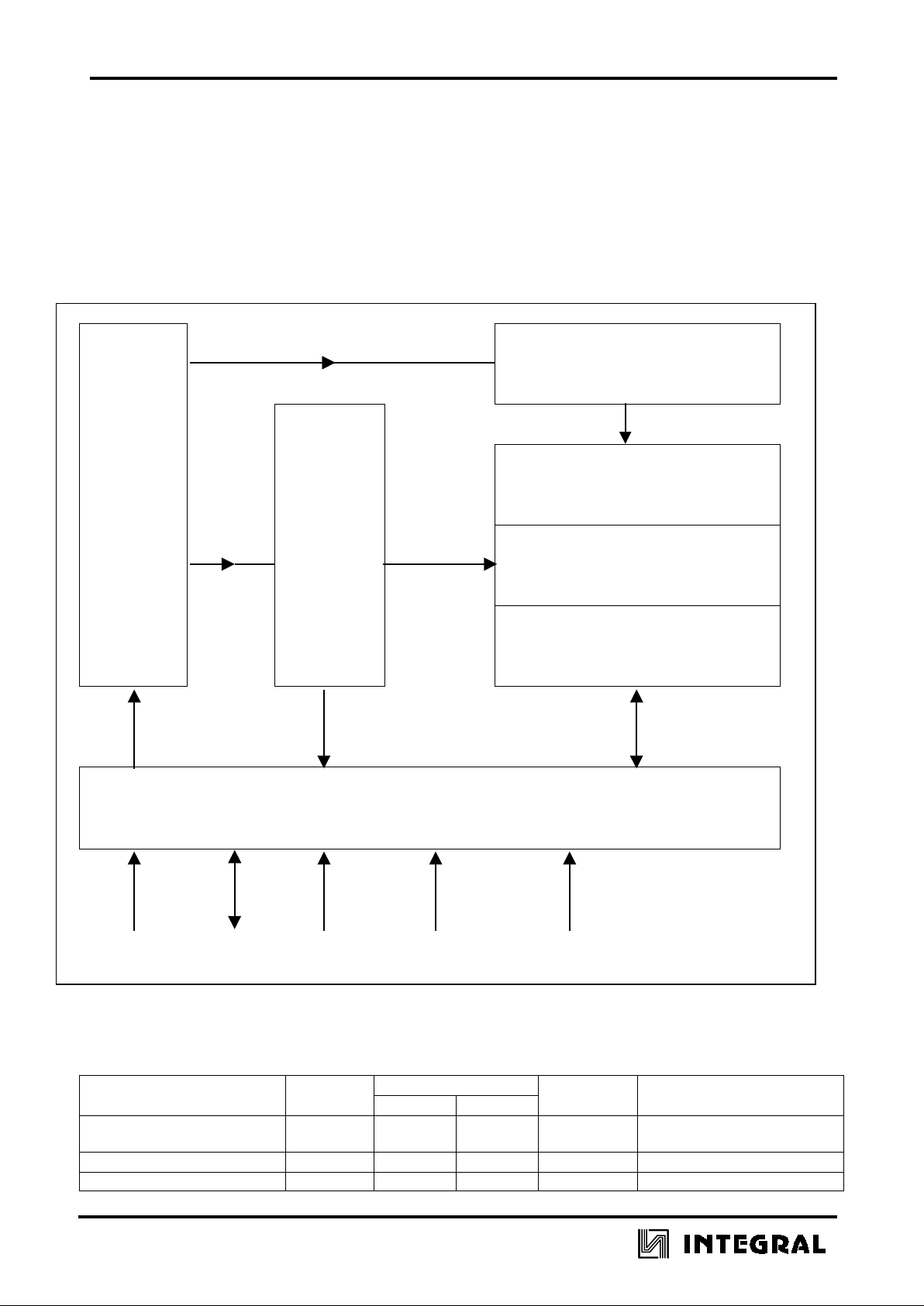
The chip contains an EEPROM/PRO M of 88 bits, a mask ROM of 16 bits and a sequencing control with
security logic (cf block diagram,
Fig. 1
).
Memory (104 bits) is divided into the following functional areas
IROM
This area contains u nalterable
chip data
(eg applicat ion, design status).
Part of the data is entered by way of a ROM mask and the remainder
when testing. Both parts are unalterable.
II PROM
In this area the user can enter
card data
for a particular application. A
control flag can be set to safeguard this area against alteration.
III PROM/EEPROM
This area contains the
count data
and stores the current count in
nonvolatile memory. The individual counter stages with carry can be
erased (ie EEPROM), only the uppermost counter stage not being
erasable (ie PROM).
Before the control flag is s et, part of the E EPROM area c ontains a sec ret
transport code
. Another part serves as an
error counter
.
Function of the PROM area:
1 bit:
Control flag
3 bits:
Test bits
for manufacturer
4 bits: for user
In the condition as supplied, the transport co de and the error counter are activat ed. The chip can only be
read (except for the transport-code area) and only the error counter can be written.
Following correct entry of the transport code, the entire memor y can be read and areas II and III can be
written and EEPROM part of area III can be erased.
IZ4406
After the control flag has been written, everything is readable and only area III can be
programmed, but with the following changes:
- The transport code and the error counter are no longer activated.
- The area of the former transport code and the error counter can be erased byte by byte
with carry.
- The entire area III can be written bit by bit
NB: When the control flag is written, the counter stage below it (the error counter) can be
erased at the same time (see “Erasing Memory Byte with Carry”).
Column Decoder,
1-out-of-8
(A0-A2)
Address
Counter
Line
Decoder
Counter
40 Bits
1-out-of-13
(A3-A6)
Blockable
PROM
40 Bits
Manufacturer
Data
24 Bits
(RAM, EEPROM)
Chip Control, Security Logic
IEB01328
CLK I/O RST GND VCC
Figure 1
Block Diagram
Absolute Maximum Ratings
Parameter Symbol Limit Values Unit Comments
Min. Max.
Supply voltage
Input voltage
V
CC
V
I
-0.3
-0.3
6
6
V
V
-
-
Storage temperature T
stg
-40 125
°C
Power dissipation P
tot
50 mW -
 Loading...