

INTEGRAL IW4518BN, IW4518BD Datasheet
Dual Up-Counter
High-Voltage Silicon-Gate CMOS
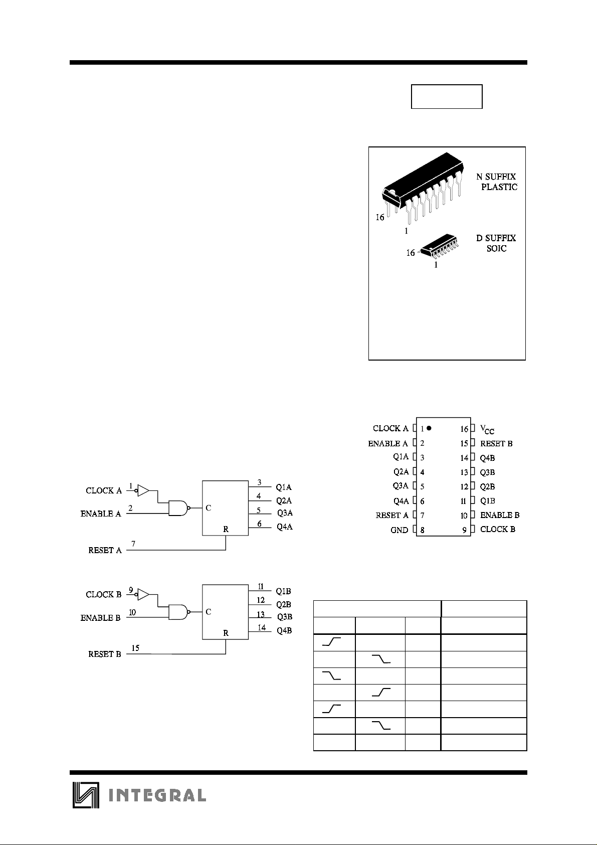
The IW4518B Dual BCD Up-Counter consists two identical,
internally synchronous 4-stage counters. The counter stages are D-type
flip-flops having interchangeable CLOCK and ENABLE lines for
incrementing on either the positive-going or negative-going transition.
For single-unit operation the ENABLE input is maintained high and
the counter advances on each positive-going transition of the CLOCK.
The counters are cleared by high levels on their RESET lines.
The counter can be cascaded in the ripple mode by connecting Q4
to the enable input of the subsequent counter while the CLOCK input
of the latter is held low.
•
Operating Voltage Range: 3.0 to 18 V
•
Maximum input current of 1 µA at 18 V over full package-
temperature range; 100 nA at 18 V and 25°C
•
Noise margin (over full package temperature range):
1.0 V min @ 5.0 V supply
2.0 V min @ 10.0 V supply
2.5 V min @ 15.0 V supply
TECHNICAL DATA
IW4518B
ORDERING INFORMATION
IW4518BN Plastic
IW4518BD SOIC
TA = -55° to 125° C for all packages
PIN ASSIGNMENT
LOGIC DIAGRAM
PIN 16=V
PIN 8= GND
CC
FUNCTION TABLE
Inputs Outputs
CLOCK ENABLE RESET Mode
H L Increment Counter
L L Increment Counter
X L No Change
X L No Change
L L No Change
H L No Change
XXHQ1 thru Q4=L
X = don’t care
163
IW4518B
MAXIMUM RATINGS
*
Symbol Parameter Value Unit
V
CC
V
V
OUT
I
IN
P
P
DC Supply Voltage (Referenced to GND) -0.5 to +20 V
DC Input Voltage (Referenced to GND) -0.5 to VCC +0.5 V
IN
DC Output Voltage (Referenced to GND) -0.5 to VCC +0.5 V
DC Input Current, per Pin
Power Dissipation in Still Air, Plastic DIP+
D
SOIC Package+
Power Dissipation per Output Transistor 100 mW
D
±
10
750
500
Tstg Storage Temperature -65 to +150
T
Lead Temperature, 1 mm from Case for 10 Seconds
L
260
(Plastic DIP or SOIC Package)
*
Maximum Ratings are those values beyond which damage to the device may occur.
Functional operation should be restricted to the Recommended Operating Conditions.
+Derating - Plastic DIP: - 10 mW/°C from 65° to 125°C
SOIC Package: : - 7 mW/°C from 65° to 125°C
RECOMMENDED OPERATING CONDITIONS
Symbol Parameter Min Max Unit
V
VIN, V
T
CC
A
DC Supply Voltage (Referenced to GND) 3.0 18 V
DC Input Voltage, Output Voltage (Referenced to GND) 0 V
OUT
Operating Temperature, All Package Types -55 +125
CC
mA
mW
°
C
°
C
V
°
C
This device c ontains p rote ction ci rcuitr y to guard a gainst damage d ue to high st atic voltages or electr ic
fields. However, precautions must be taken to avoid applications of any voltage higher than maximum rated
voltages to this high-impedance circuit. For proper operation, V
GND≤(V
IN
or V
OUT
)≤VCC.
Unused inputs must always be tied to an appropriate logic voltage level (e.g., either GND or V
and V
IN
should be constrained to the range
OUT
CC
Unused outputs must be left open.
164
).
 Loading...