

Page 1
查询IW4069BE供应商
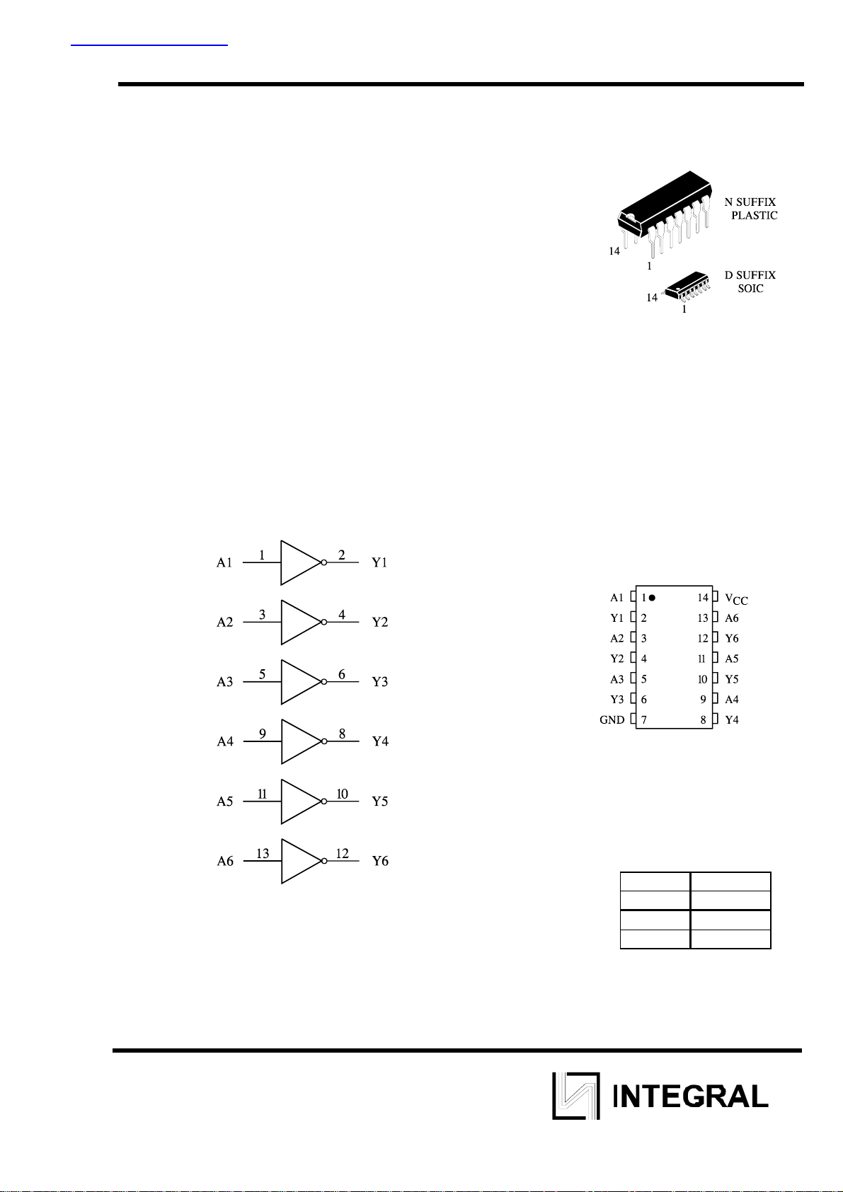
The IW4069UB types consist of six inverter circuits. These
devices are intended for all general-purpose inverter applications
where the medium-power TTL-drive and logic-level-conversion
capabilities of circuits such as the IW4049UB Hex Inverter/Buffers
are not required. Each of the six inverters is a single stage
• Operating Voltage Range: 3.0 to 18 V
• Maximum input current of 1 µA at 18 V over full package-
temperature range; 100 nA at 18 V and 25°C
• Noise margin (over full package temperature range):
0.5 V min @ 5.0 V supply
1.0 V min @ 10.0 V supply
1.0 V min @ 15.0 V supply
IW4069UB
HEX INVERTER
High-Voltage Silicon-Gate CMOS
ORDERING INFORMATION
IW4069UBN Plastic
IW4069UBD SOIC
T
= -55° to 125° C for all
A
packages
LOGIC DIAGRAM
PIN 14 =V
CC
PIN 7 = GND
PIN ASSIGNMENT
FUNCTION TABLE
Inputs Output
A Y
L H
H L
1
Page 2
IW4069UB
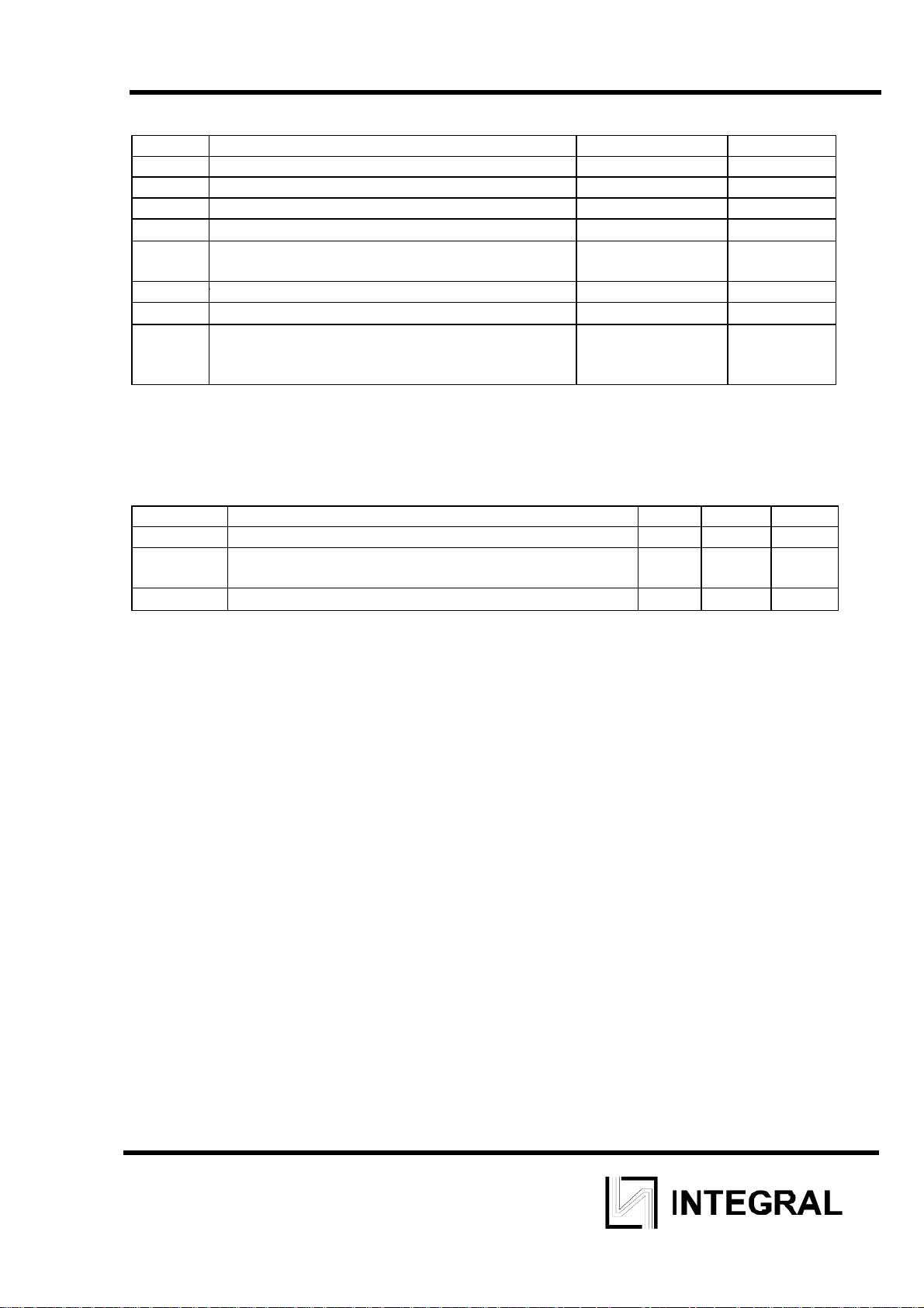
MAXIMUM RATINGS
*
Symbol Parameter Value Unit
VCC DC Supply Voltage (Referenced to GND) -0.5 to +20 V
VIN DC Input Voltage (Referenced to GND) -0.5 to VCC +0.5 V
V
DC Output Voltage (Referenced to GND) -0.5 to VCC +0.5 V
OUT
IIN DC Input Current, per Pin
PD Power Dissipation in Still Air, Plastic DIP+
SOIC Package+
PD
Dissipation per Output Transistor 100 mW
±10
750
500
Tstg Storage Temperature -65 to +150
TL Lead Temperature, 1 mm from Case for 10
260
mA
mW
°C
°C
Seconds
(Plastic DIP or SOIC Package)
*
Maximum Ratings are those values beyond which damage to the device may occur.
Functional operation should be restricted to the Recommended Operating Conditions.
+Derating - Plastic DIP: - 10 mW/°C from 65° to 125°C
SOIC Package: : - 7 mW/°C from 65° to 125°C
RECOMMENDED OPERATING CONDITIONS
Symbol Parameter Min Max Unit
VCC DC Supply Voltage (Referenced to GND) 3.0 18 V
VIN, V
DC Input Voltage, Output Voltage (Referenced to
OUT
0 VCC V
GND)
TA Operating Temperature, All Package Types -55 +125
°C
This device contains protection circuitry to guard against damage due to high static
voltages or electric fields. However, precautions must be taken to avoid applications of any voltage
higher than maximum rated voltages to this high-impedance circuit. For proper operation, V
V
should be constrained to the range GND≤(VIN or V
OUT
OUT
)≤VCC.
and
IN
Unused inputs must always be tied to an appropriate logic voltage level (e.g., either GND or
V
). Unused outputs must be left open.
CC
2
Page 3

IW4069UB
DC ELECTRICAL CHARACTERISTICS(Voltages Referenced to GND)
V
CC
Symbol Parameter Test Conditions V
VIH Minimum High-
Level Input
Voltage
VIL Maximum Low -
Level Input
Voltage
VOH Minimum High-
Level Output
Voltage
VOL Maximum Low-
Level Output
Voltage
IIN Maximum Input
V
=0.5V
OUT
V
=1.0 V
OUT
V
=1.5V
OUT
V
= V
= V
= V
- 0.5 V
CC
- 1 V
CC
- 1.5 V
CC
OUT
V
OUT
V
OUT
V
=GND 5.0
IN
V
= VCC 5.0
IN
VIN= GND or VCC 18
5.0
10
15
5.0
10
15
10
15
10
15
Leakage Current
ICC Maximum
Quiescent Supply
Current
(per Package)
IOL Minimum Output
Low (Sink)
Current
IOH Minimum Output
High (Source)
Current
V
= GND or VCC 5.0
IN
V
= GND or VCC
IN
U
=0.4 V
OL
U
=0.5 V
OL
U
=1.5 V
OL
V
= GND or VCC
IN
U
=2.5 V
OH
U
=4.6 V
OH
U
=9.5 V
OH
U
=13.5 V
OH
10
15
20
5.0
10
15
5.0
5.0
10
15
Guaranteed Limit
≥-55°C 25°C ≤125
4
8
12.5
1
2
2.5
4.95
9.95
14.95
0.05
0.05
0.05
±0.1 ±0.1 ±1.0 µA
0.25
0.5
1.0
5.0
0.64
1.6
4.2
-2.0
-0.64
-1.6
-4.2
4
8
12.5
1
2
2.5
4.95
9.95
14.95
0.05
0.05
0.05
0.25
0.5
1.0
5.0
0.51
1.3
3.4
-1.6
-0.51
-1.3
-3.4
°C
4
8
12.5
1
2
2.5
4.95
9.95
14.9
5
0.05
0.05
0.05
7.5
15
30
150
0.36
0.9
2.4
-1.15
-0.36
-0.9
-2.4
Unit
V
V
V
V
µA
mA
mA
3
Page 4

IW4069UB
AC ELECTRICAL CHARACTERISTICS(C
V
Symbol Parameter V
t
,
Maximum Propagation Delay, Input A to
Output Y (Figure 1)
Maximum Output Transition Time, Any
THL
t
TLH
PLH
t
PHL
, t
Output (Figure 1)
CIN Maximum Input Capacitance - 15 pF
=50pF, RL=200kΩ, Input tr=tf=20 ns)
L
CC
Guaranteed Limit
≥-55
25°C ≤125
°C
5.0
10
15
5.0
10
15
110
60
50
200
100
80
110
60
50
200
100
80
°C
220
120
100
400
200
160
Unit
ns
ns
Figure 1. Switching Waveforms
EXPANDED LOGIC DIAGRAM
(1/6 of the Device)
4
 Loading...