

INTEGRAL IW4043BN, IW4043BD Datasheet
TECHNICAL DATA
Quad 3-State R/S Latches
High-Voltage Silicon-Gate CMOS
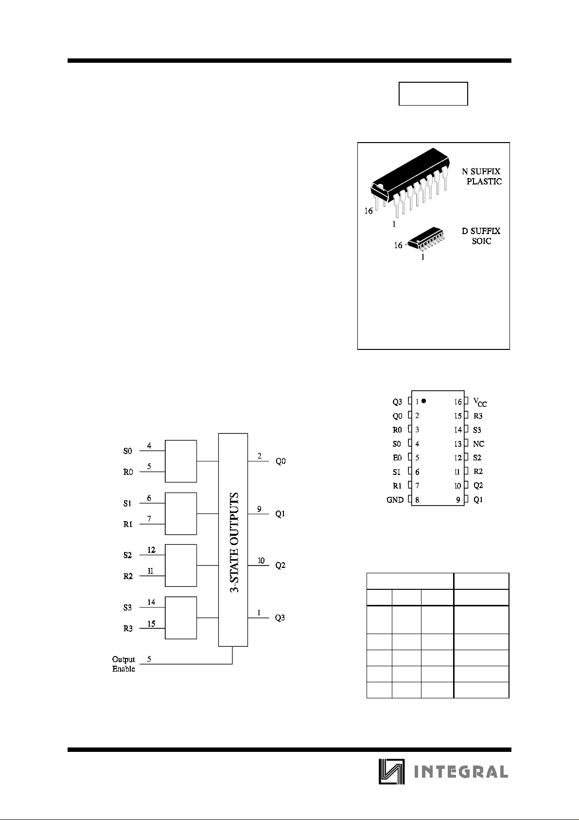
The IW4043B types are quad cross-coupled 3-state CMOS NOR
latces. Each latch has a separate Q output and individual SET and
RESET inputs. The Q outputs are controlled by a common ENABLE
input. A logic “1” or high on the ENABLE input connects the latch
states to the Q outputs. A logic “0” or low on the ENABLE input
disconnects the latch states from the Q outputs, resulting in an open
circuit condition on the Q outputs. The open circuit feature allows
common busing of the outputs.
•
Operating Voltage Range: 3.0 to 18 V
•
Maximum input current of 1 µA at 18 V over full package-
temperature range; 100 nA at 18 V and 25°C
•
Noise margin (over full package temperature range):
1.0 V min @ 5.0 V supply
2.0 V min @ 10.0 V supply
2.5 V min @ 15.0 V supply
IW4043B
ORDERING INFORMATION
IW4043BN Plastic
IW4043BD SOIC
TA = -55° to 125° C for all packages
LOGIC DIAGRAM
PIN 13 = NO CONNECTION
PIN 16=V
PIN 8= GND
CC
PIN ASSIGNMENT
FUNCTION TABLE
Inputs Outputs
SROE Q
XX L High
Impedance
L L H No change
LH H L
HL H H
HH H H
X = don’t care
84
IW4043B
MAXIMUM RATINGS
*
Symbol Parameter Value Unit
V
CC
V
V
OUT
I
IN
P
P
DC Supply Voltage (Referenced to GND) -0.5 to +20 V
DC Input Voltage (Referenced to GND) -0.5 to VCC +0.5 V
IN
DC Output Voltage (Referenced to GND) -0.5 to VCC +0.5 V
DC Input Current, per Pin
Power Dissipation in Still Air, Plastic DIP+
D
SOIC Package+
Power Dissipation per Output Transistor 100 mW
D
±
10
750
500
Tstg Storage Temperature -65 to +150
T
Lead Temperature, 1 mm from Case for 10 Seconds
L
260
(Plastic DIP or SOIC Package)
*
Maximum Ratings are those values beyond which damage to the device may occur.
Functional operation should be restricted to the Recommended Operating Conditions.
+Derating - Plastic DIP: - 10 mW/°C from 65° to 125°C
SOIC Package: : - 7 mW/°C from 65° to 125°C
RECOMMENDED OPERATING CONDITIONS
Symbol Parameter Min Max Unit
V
VIN, V
T
CC
A
DC Supply Voltage (Referenced to GND) 3.0 18 V
DC Input Voltage, Output Voltage (Referenced to GND) 0 V
OUT
Operating Temperature, All Package Types -55 +125
CC
mA
mW
°
C
°
C
V
°
C
This device c ontains p rote ction ci rcuitr y to guard a gainst damage d ue to high st atic voltages or electr ic
fields. However, precautions must be taken to avoid applications of any voltage higher than maximum rated
voltages to this high-impedance circuit. For proper operation, V
GND≤(V
IN
or V
OUT
)≤VCC.
Unused inputs must always be tied to an appropriate logic voltage level (e.g., either GND or V
and V
IN
should be constrained to the range
OUT
CC
Unused outputs must be left open.
85
).
 Loading...