

INTEGRAL IW4042BN, IW4042BD Datasheet

Quad Clocked «D» Latch
High-Voltage Silicon-Gate CMOS
CD4042B types contain four latch circuits, each strobed by a
common clock. Complementary buffered outputs are available from
each circuit. The impedance of the n- and p-channel output devices is
balanced and all outputs are electrically identical. Information present
at the data input is transferred to outputs Q and Q during the CLOCK
level which is programmed by the POLARITY input. For
POLARITY = 0 the transfer occurs during the 0 CLOCK level and for
POLARITY = 1 the transfer occurs during the 1 CLOCK level. The
outputs follow the data input providing the CLOCK and POLARITY
levels defined above are present. When a CLOCK transition occurs
(positive for POLARITY = 0 and negative for POLARTY = 1) the
information present at the input during the CLOCK transition is
retained at the outputs until an opposite CLOCK transition occurs.
The CD4042B types are supplied in 16-lead hermetic dual-in-line
ceramic packages (D and F suffixes); 16-lead dual-in-line plastic
package (E suffix), and in chip form (H suffix).
•
Operating Voltage Range: 3.0 to 18 V
•
Maximum input current of 1 µA at 18 V over full package-
temperature range; 100 nA at 18 V and 25°C
•
Noise margin (over full package temperature range):
1.0 V min @ 5.0 V supply
2.0 V min @ 10.0 V supply
2.5 V min @ 15.0 V supply
TECHNICAL DATA
IW4042B
ORDERING INFORMATION
IW4042BN Plastic
IW4042BD SOIC
TA = -55° to 125° C for all packages
PIN ASSIGNMENT
LOGIC DIAGRAM
PIN 16 =V
PIN 8 = GND
CC
FUNCTION TABLE
Inputs Outputs
Clock Polarity Q
00D
10Latch
11D
01Latch
1
IW4042B
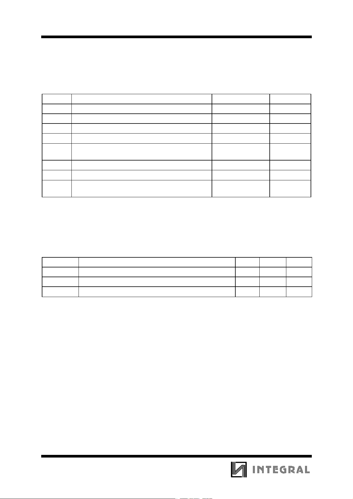
MAXIMUM RATINGS
*
Symbol Parameter Value Unit
V
CC
V
V
OUT
I
P
DC Supply Voltage (Referenced to GND) -0.5 to +20 V
DC Input Voltage (Referenced to GND) -0.5 to VCC +0.5 V
I
DC Output Voltage (Referenced to GND) -0.5 to VCC +0.5 V
DC Input Current, per Pin
I
Power Dissipation in Still Air, Plastic DIP+
D
SOIC Package+
±
10
750
500
Ptot Power Dissipation per Output Transistor 100 mW
Tstg Storage Temperature -65 to +150
T
Lead Temperature, 1 mm from Case for 10 Seconds
L
260
(Plastic DIP or SOIC Package)
*
Maximum Ratings are those values beyond which damage to the device may occur.
Functional operation should be restricted to the Recommended Operating Conditions.
+Derating - Plastic DIP: - 10 mW/°C from 65° to 125°C
SOIC Package: : - 7 mW/°C from 65° to 125°C
RECOMMENDED OPERATING CONDITIONS
Symbol Parameter Min Max Unit
V
VI, V
T
CC
OUT
A
DC Supply Voltage (Referenced to GND) 3.0 18 V
DC Input Voltage, Output Voltage (Referenced to GND) 0 V
CC
Operating Temperature, All Package Types -55 +125
mA
mW
°
C
°
C
V
°
C
This device contains protection circuitry to guard against damage due to high static voltages or electric
fields. However, precautions must be taken to avoid applications of any voltage higher than maximum rated
voltages to this high-impedance circuit. For proper operation, V
GND≤(V
IN
or V
OUT
≤
)
.
VCC
Unused inputs must always be tied to an appropriate logic voltage level (e.g., either GND or
and V
IN
should be constrained to the range
OUT
VCC
Unused outputs must be left open.
2
).
 Loading...