

INTEGRAL IW4034BN, IW4034BDW Datasheet
TECHNICAL DATA
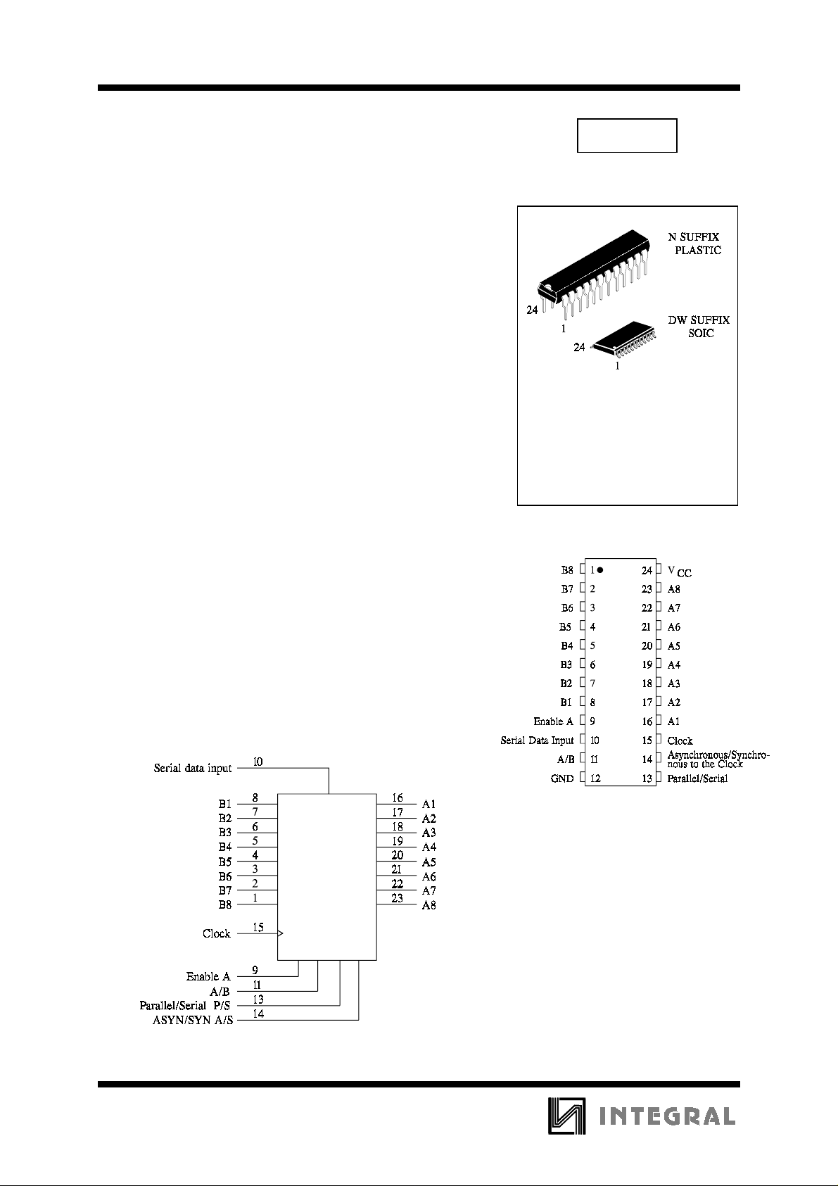
IW4034B
8-Stage Static Bidirectional Parallel/
Serial Input/Output Bus Register
High-Voltage Silicon-Gate CMOS
The IW4034B is a static eight-stage parallel-or serial-input
parallel-output register. It can be used to:
1) bidirectionally transfer parallel information between two buses,
2) convert serial data to parallel form and direct the parallel data to
either of two buses, 3) store (recirculate) parallel data, or 4) accept
parallel data from either of two buses and convert that data to serial
form. Inputs that control the operations include a single-phase CLOCK
(CL), A DATA ENABLE (AE),
ASYNCHRONOUS/SYNCHRONOUS (A/S), A-BUS-TO-B-BUS/ BBUS-TO-A-BUS (A/B), and PARALLEL/SERIAL (P/S).
Data inputs include 16 bidirectional parallel data lines of which the
eight A data lines are inputs (3-state outputs) and the B data lines are
outputs (inputs) dependung on the signal level on the A/B input. In
addition, an input for SERIAL DATA is also provided.
All register stages are D-type master-slave flip-flops with separate master and slave clock inputs generated
internally to allow synchronous or asynchronous data transfer from
master to slave.
•
Operating Voltage Range: 3.0 to 18 V
•
Maximum input current of 1 µA at 18 V over full package-
temperature range; 100 nA at 18 V and 25°C
•
Noise margin (over full package temperature range):
1.0 V min @ 5.0 V supply
2.0 V min @ 10.0 V supply
2.5 V min @ 15.0 V supply
ORDERING INFORMATION
IW4034BN Plastic
IW4034BDW SOIC
TA = -55° to 125° C for all packages
PIN ASSIGNMENT
76
LOGIC DIAGRAM
PIN 24=V
PIN 12= GND
CC
IW4034B
MAXIMUM RATINGS
*
Symbol Parameter Value Unit
V
CC
V
V
OUT
I
IN
P
P
DC Supply Voltage (Referenced to GND) -0.5 to +20 V
DC Input Voltage (Referenced to GND) -0.5 to VCC +0.5 V
IN
DC Output Voltage (Referenced to GND) -0.5 to VCC +0.5 V
DC Input Current, per Pin
Power Dissipation in Still Air, Plastic DIP+
D
SOIC Package+
Power Dissipation per Output Transistor 100 mW
D
±
10
750
500
Tstg Storage Temperature -65 to +150
T
Lead Temperature, 1 mm from Case for 10 Seconds
L
260
(Plastic DIP or SOIC Package)
*
Maximum Ratings are those values beyond which damage to the device may occur.
Functional operation should be restricted to the Recommended Operating Conditions.
+Derating - Plastic DIP: - 10 mW/°C from 65° to 125°C
SOIC Package: : - 7 mW/°C from 65° to 125°C
RECOMMENDED OPERATING CONDITIONS
Symbol Parameter Min Max Unit
V
VIN, V
T
CC
A
DC Supply Voltage (Referenced to GND) 3.0 18 V
DC Input Voltage, Output Voltage (Referenced to GND) 0 V
OUT
Operating Temperature, All Package Types -55 +125
CC
mA
mW
°
C
°
C
V
°
C
This device c ontains p rote ction ci rcuitr y to guard a gainst damage d ue to high st atic voltages or electr ic
fields. However, precautions must be taken to avoid applications of any voltage higher than maximum rated
voltages to this high-impedance circuit. For proper operation, V
GND≤(V
IN
or V
OUT
)≤VCC.
Unused inputs must always be tied to an appropriate logic voltage level (e.g., either GND or V
and V
IN
should be constrained to the range
OUT
CC
Unused outputs must be left open.
77
).
IW4034B
DC ELECTRICAL CHARACTERISTICS
(Voltages Referenced to GND)
Symbol Parameter Test Conditions V
V
V
V
IH
IL
OH
Minimum High-Level
Input Voltage
Maximum Low -Level
Input Voltage
Minimum High-Level
V
= 0.5 V or V
OUT
V
= 1.0 V or V
OUT
V
= 1.5 V V
OUT
V
= 0.5 V or V
OUT
V
= 1.0 V or V
OUT
V
= 1.5 V V
OUT
VIN=GND or V
CC
CC
CC
- 0.5V
CC
- 1.0 V
CC
- 1.5V
- 0.5V
CC
- 1.0 V
CC
- 1.5V
Output Voltage
V
OL
Maximum Low-Level
VIN=GND or V
CC
Output Voltage
I
IN
Maximum Input
VIN= GND or V
CC
Leakage Current
I
OZ
I
CC
Minimum Three State
Leakage Current
Maximum Quiescent
Output in High-Impedance
State
V
= GND or V
IN
V
= GND or V
OUT
VIN= GND or V
CC
CC
CC
Supply Current
(per Package)
I
OL
I
OH
Minimum Output Low
(Sink) Current
Minimum Output
High (Source) Current
VIN= GND or V
UOL=0.4 V
U
=0.5 V
OL
U
=1.5 V
OL
VIN= GND or V
UOH=2.5 V
U
=4.6 V
OH
U
=9.5 V
OH
U
=13.5 V
OH
CC
CC
V
5.0
10
15
5.0
10
15
5.0
10
15
5.0
10
15
18
18
5.0
10
15
20
5.0
10
15
5.0
5.0
10
15
CC
≥
14.95
Guaranteed Limit
-55°C25°C
3.5
7
11
1.5
3
4
4.95
9.95
3.5
7
11
1.5
3
4
4.95
9.95
14.95
0.05
0.05
0.05
±
0.1
±
0.4
5
10
20
100
0.64
1.6
4.2
-2
-0.64
-1.6
-4.2
0.05
0.05
0.05
±
0.1
±
0.4
5
10
20
100
0.51
1.3
3.4
-1.6
-0.51
-1.3
-3.4
≤
125
°
C
3.5
7
11
1.5
3
4
4.95
9.95
14.95
0.05
0.05
0.05
±
1.0
±
12.0
150
300
600
3000
0.36
0.9
2.4
-1.15
-0.36
-0.9
-2.4
Unit
V
V
V
V
µ
A
µ
A
µ
A
mA
mA
78
 Loading...