

INTEGRAL INF8594E Datasheet
ICs for TV-SETS
INF8594E
512 x 8-Bit CMOS EEPROM with I2C-Bus Interface
The INF8594E-2 is a 4-Kbit (512 x 8-bit) floating gate electrically erasable programmable read only memory
(EEPROM). By using an internal redundant storage code it is fault tolerant to single bit errors. This feature dramatically
increases reliability. IC works in systems with serial
2
I
C-bus which consists of 2 lines: for data -serial data input/output (SDA) and for clock - serial clock input (SCL). Up to four
INF8594E-2 devices may be connected to the I
of the array is implemented by electron’s tunneling. The programming voltage is generated on-chip, using a voltage multiplier.
Power consumption is low owing to the full CMOS technology used. Device is functionally identical to the PCF8594E-2, Philips.
IC are made in 8-pin DIP and 8-pin SOP.
FEATURES
♦ Low Power CMOS
maximum active current 2.5 mA
maximum standby current 10 µA
♦ Non-volatile storage of 4-Kbits organized as two pages each 256 x 8-bits
♦ Single supply (Ucc=4,5 B - 5,5 B)
♦ On-chip voltage multiplier
♦ Serial input/output I
♦ Automatically added word address
♦ Internal timer for writing (no external components)
100 000 ERASE/WRITE cycles per byte;
♦ Write operations
-byte write mode
-8-byte page write mode (minimizes total write time per byte)
♦ Write protection input
♦ Read operations
sequential read
random read
♦ Power-on reset
♦ High reliability by using a redundant storage code (single bit error correction)
♦ Endurance
100 k; T
10 years non-volatile data retention time
♦ Pin and Address compatible to PCx8582x-2 Family and PCx8598x2 Family
♦ Temperature range: -40
amb
=850C
2
C-bus
0
C ÷ +850C
2
C-bus.The programming
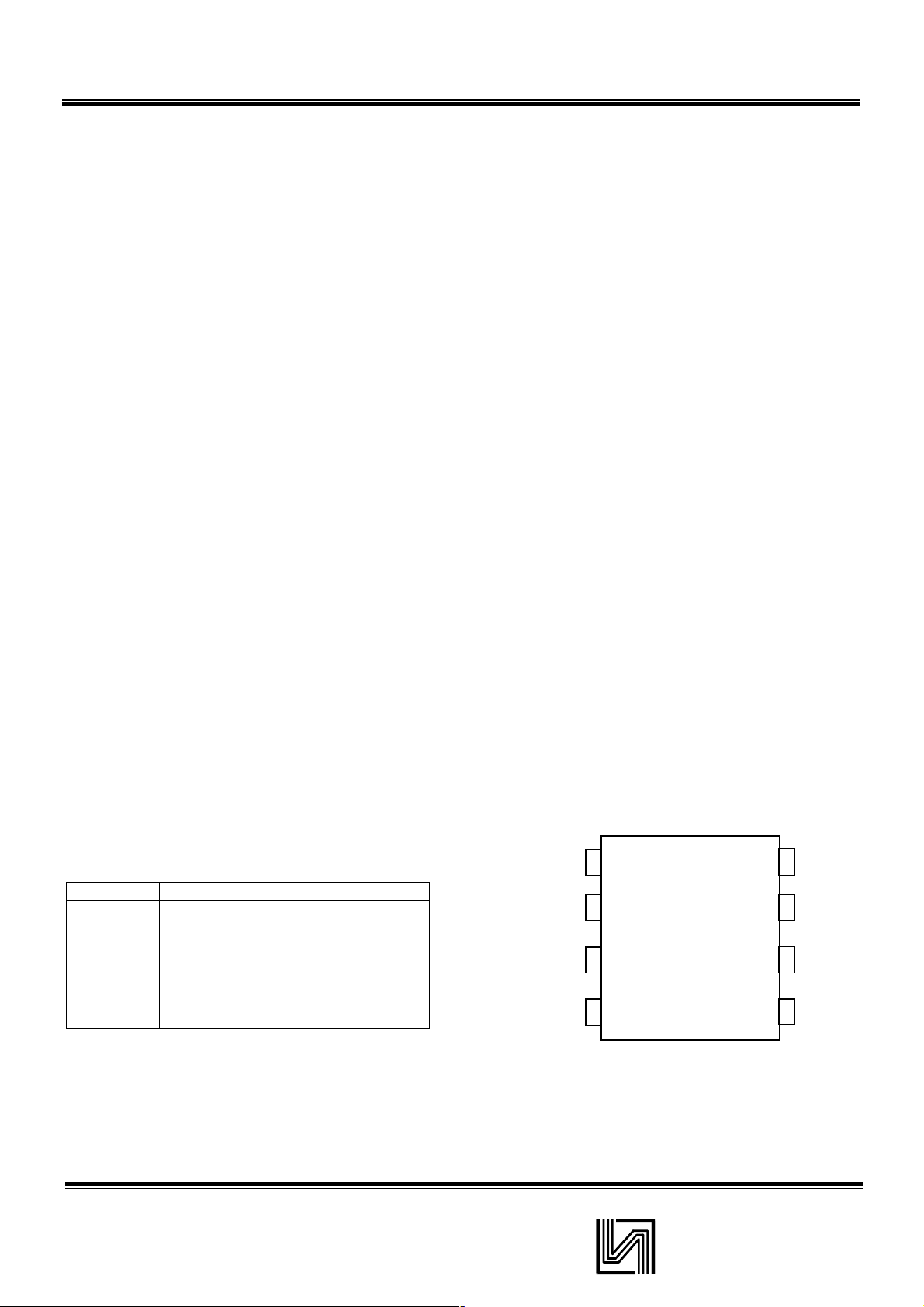
PIN DESCRIPTION
SYMBOL PIN DESCRIPTION
WRITE protection input
WP
A1
A2
Uss
SDA
SCL
PTC
Ucc
1
address input 1
2
address input 2
3
«GND»
4
Informational line, input/output
5
Clock line, input
6
programming management
7
Supply voltage
8
PIN ASSIGNMENT
WP
Uss
A1
A2
1
2
3
4
8
7
6
5
Ucc
PTC
SCL
SDA
1
INTEGRAL
ICs for TV-SETS
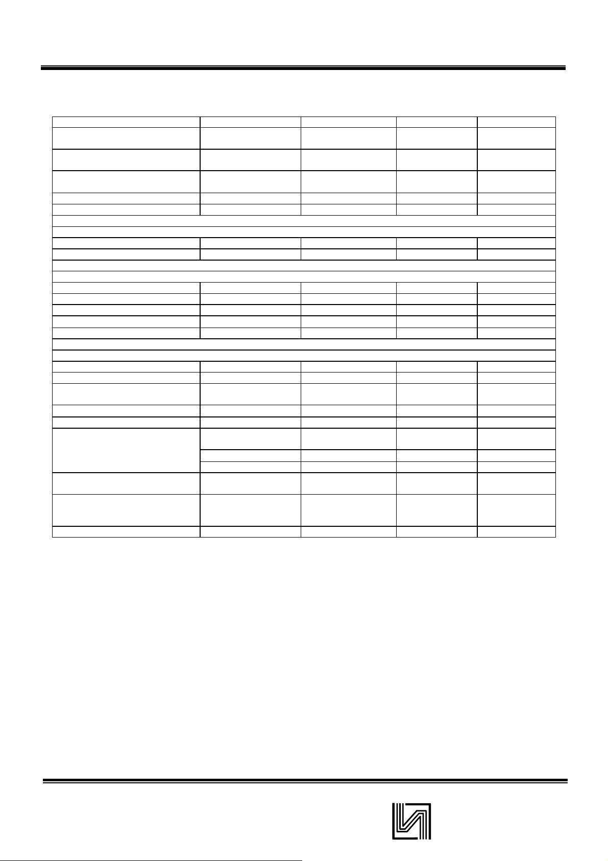
Electrical Characteristics
Parameter Conditions Symbol Min. Max
Supply current READ,mkA f
Supply current ERASE/WRITE,
mA
Standby Supply
Current, µA
Clock input frequency, kHz f
E/WR cycle time, ms t
Input high voltage, V U
Input low voltage, V U
Input high voltage, V U
Input low voltage, V U
Clock input frequency, kHz f
Leakage current, µA
Input capacitance, pF UI=GND C
=100kHz
SCL
U
=5.5B
CC
f
=100kHz
SCL
U
=5.5B
CC
UCC=5,5B I
PTC input
SCL inputs
=Ucc or GND I
U
I
I
CC0(RD)
I
CC0(E/WR)
CCS
SCL
E/WR
IH
IL
IH
IL
SCL
LI
I
- 200
-2,5
- 10.0
0 100
410
0,9U
CC
-0,8 0,1U
0,7U
CC
-0,8 0,3U
0 100
INF8594E
UCC+0,8
CC
UCC+0,8
CC
±1µA
7
SDA input/output
Low input voltage, V U
High input voltage, V U
Low level output voltage, V IOL=3мА,
IL
IH
U
OL
-0.8 0.3U
0.7Ucc UCC+0.8
Ucc=Uccmin
Output leakage current, µA
Input capacitance, pF UI=0B С
UOH=Ucc I
LO
I
Duration of the ERASE/WRITE
cycle
-internal generator t
E/WR
4∗ 10∗
-external clock signal 4 10
Frequency of the external clock
fp 25 60
programming signals, kHz
Number of the ERASE/WRITE
cycles per byte
Т=-40-+85оС,
t
=4-10 мс,
E/W
о
Т=22
С, t
E/W
=5 мс
Time of data storage Т = 55оС t
N
E/W
100 000
10 000
S
10
CC
0.4
1
7
2
INTEGRAL
 Loading...