

INTEGRAL INA2586 Datasheet
ICs for TV-SETS
1024 x 8-Bit n-MOS EEPROM with I2C-Bus Interface
INA2586
The INA2586 is a 8-Kbit (1024 x 8-bit) n-MOS floating gate electrically erasable programmable read only memory (EEPROM).
IC works in systems with serial I
2
C-bus. Up to two INA2586 devices may be connected to the I2C-bus.The programming of the
array is implemented by electron’s tunneling. The programming voltage is generated on-chip, using a voltage multiplier. Device
is functionally identical to the SDA2586, Siemens. IC are made in 8-pin DIP and 8-pin SOP.
FEATURES
♦ Non-volatile storage of information during 10 years
♦ Single supply (Ucc=4,75 B - 5,25 B)
♦ On-chip voltage multiplier
♦ On-chip generator of bulk biasing
♦ Serial input/output I
2
C-bus
♦ 10 000 ERASE/WRITE cycles per byte;
♦ Internal reprogramming (no external components)
♦ Duration of the ERASE/WRITE cycle is 15 ms
♦ Temperature range: 0 ÷ +70
0
C
ELECTRICAL CHARACTERISTICS
Parameter Conditions Symbol Min. Max
Supply current, mA UCC=5.25 B I
Output low voltage (SDA), V IOL=3 mA
U
=4.75B
CC
U
CC0
OL
- 20,0
-0,4
High leakage current:
-on output (SDA), µA
-on inputs SCL, SDA, µA
-on inputs CS, TP1, TP2,µA
U
OH
U
IH
U
IH
=5,25 B
=5,25 B
=5,25 B
I
I
I
Input capacitance, pF UI= 0 B C
Clock input frequency, kHz f
Reprogramming cycle time, ms Erase and Write t
Erase of die cycle time, ms U
= 5,0 B t
TP2
PROG
LOH
LIH
LIH
SCL
ER
-
-
-
I
- 10,0
0 100
10,0 20,0
- 20,0
10,0
10,0
100,0
The number of E/W cycles on 1 byte 10 000 Input high voltage:
-inputs SDA, SCL, V
-inputs CS, TP1, TP2, V
U
IH
3,0
4,5
U
CC
U
CC
Input low voltage:
-inputs SDA, SCL, V
-inputs CS, TP1, TP2, V
U
IL
-
-
1,5
0,2
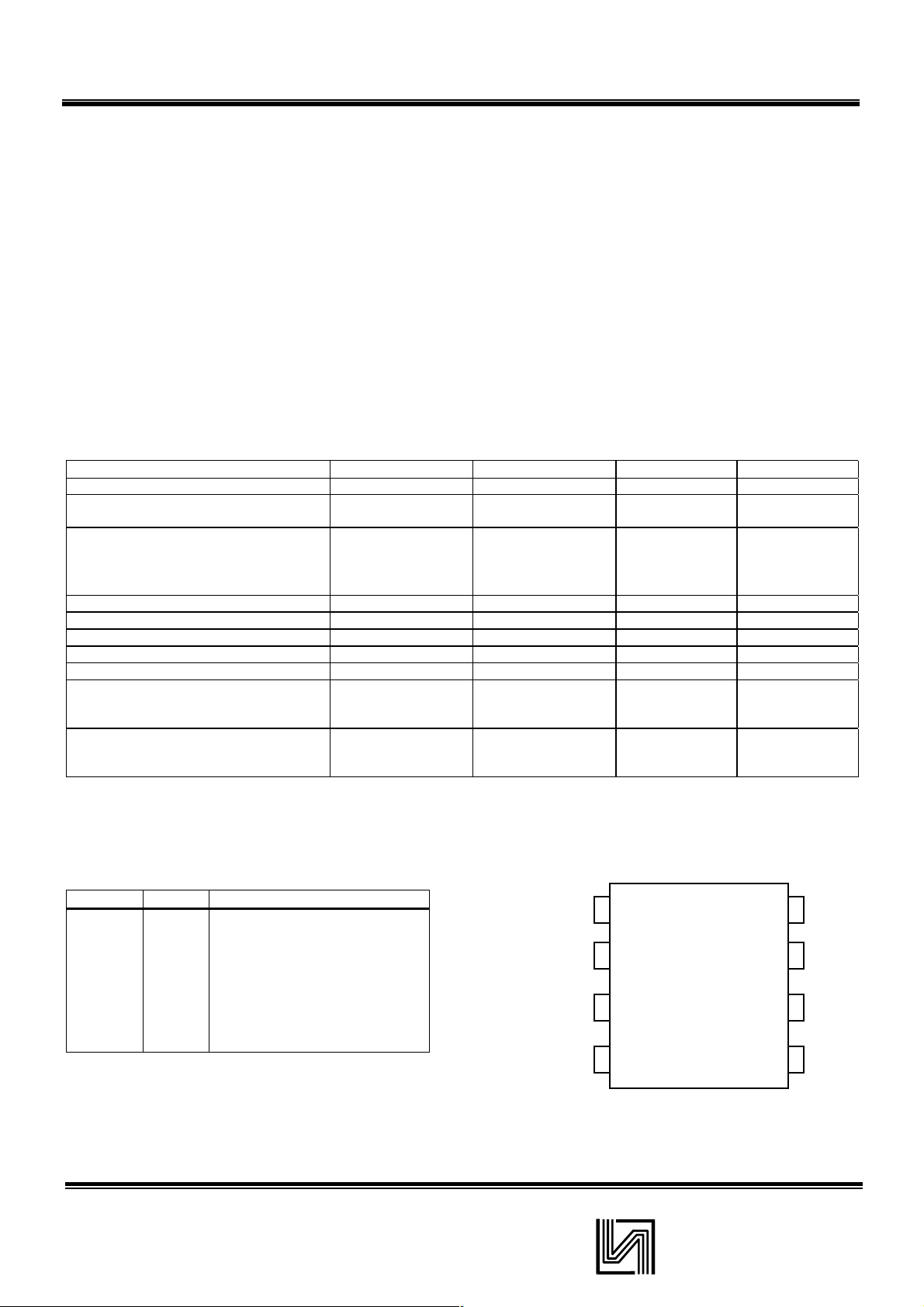
PIN DESCRIPTION
SYMBOL PIN DESCRIPTION
GND
Uss
CS
TP1
TP2
SDA
SCL
TP3
Ucc
1
Chip selection
2
Testing pin
3
Testing pin (0V - normal mode,
4
5V - chip erasing)
5
Informational line, input/output
6
Clock input
7
Testing pin, not connected
8
Supply Voltage
PIN ASSIGNMENT
Uss
CS
TP1
TP2
1
2
3
4
8
7
6
5
Ucc
TP3
SCL
SDA
1
INTEGRAL
 Loading...