

INTEGRAL IN915531N Datasheet
TECHNICAL DATA
1
PARALLEL INPUT TONE/PULSE DIALER
High-Performance Silicon-Gate CMOS
The IN91531 provides a 4-bit data input and a handshaking signal
to serve as microcomputer interfaces. Under microcomputer control the
IN91531 generates both a DTMF signal and a pulse output for telephone
dialing. All necessary dual-tone frequencies and dial pulse outputs are
derived from the widely used TV crystal standard, providing high
accuracy and stability. The required sinusoidal waveform for individual
tones is digitally synthesized on the chip, resulting in a waveform with
very low total harmonic distortion.
•
4-bit parallel data input from microcomputer
•
TTL compatible inputs and outputs
•
Uses TV crystal standard (3.58 MHz) to derive all frequencies,
providing high accuracy and stability
•
Operating voltage: 2.5 to 5.5 Volts
•
Selectable M/B ratio
•
10 PPS dial rate
•
DTMF signaling of digits 0 9, *, #, A, B, C, and D
•
Pulse signaling of 0 ∼ 9, *, #, and A
•
High group tone pre-emphasis: 2 dB
•
Low total harmonic distortion in DTMF signaling
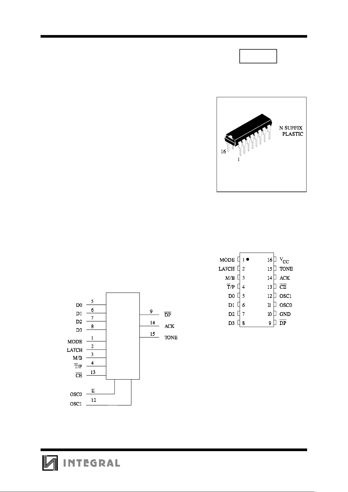
IN91531
ORDERING INFORMATION
IN91531N
TA = -10° to 70° C
PIN ASSIGNMENT
LOGIC DIAGRAM
PIN 10 = GND
PIN 16 = V
CC
IN91531
2
PIN DESCRIPTION
Pin No. Designation
DESCRIPTION
1 MODE Tone mode select input.
When this input is high, the tone output and ASK output are normal. When this input is
low, a DTMF signal will be generated continuously and any new input data will be
ignored.
This input affects the tone output mode only.
2 LATCH Latch input.
When input on this pin changes from low to high (at the rising edge), the IN91531 latches
the 4-bit input data and T/P input. The latch input should not be changed back from low to
high again until the ASK output falls low, and new data must not be latched while the
ASK output is still low.
3 M/B Make/Break ratio select input.
This pin is used to select one of two available make/break ratios. A high input selects the
2/3 make/break ratio; a low input selects the 1/23 ratio. This input should be connected to
V
CC
or GND only. Changing the state of this pin when CE is active (low) enables the test
mode.
4 T/P Tone/pulse mode select input.
This input determines whether tone or pulse mode will be activated. It is latched together
with the 4-bit data input.
5 - 8 D0 - D3 4-bit data input pins.
This 4-bit parallel input is used to receive data generated by the microcomputer. (Input
data vs. output signal is shown in table 1.) Valid input data should be presented at these
inputs before and during the rising edge of the latch signal.
9 DP Dial pulse output.
The dial pulse output consists of an N-channel open drain device. During dial pulse break
periods this output is switched on (sinking current to GND); it is switched off during all
other states. Dialing rate is 9.71 PPS and post-digit pause is 823 ms. (The output of this
pin during test mode is discussed below.)
10
16
GND
V
CC
Negative power supply input.
Positive power supply input (operating range 2.5 to 5.5 volts).
11
12
OSC0
OSC1
Oscillator output.
Oscillator input.
The IN91531 contains an oscillator circuit with the necessary parasitic capacitance and
feedback resistor on chip, making it necessary to connect only a standard 3.58 MHz TV
crystal across the OSC1 and OSC0 terminals to implement the oscillator function. An
external clock input can be applied to the OSC1 pin directly. The oscillator is enabled
when the CE input is low.
13 CE Chip enable input.
This input controls the onset of oscillation and serves as the master reset for this device.
14 ASK Acknowledge output.
This pin provides an acknowledge signal to the microcomputer. This output is high when
the device is ready to dial out the next digit; it falls low immediately after the rising edge
of the latch signal.
15 TONE DTMF signal output.
This pin consists of an NPN transistor output, with the collector connected to V
CC
. This
pin is also connected to the emitter output. The internally generated DTMF signal is
delivered to the base of the NPN transistor and is amplified as the transistor connected in
common collector. DTMF signaling output time is 70 ms and the interdigit interval is
70 ms. Typical output impedance of the DTMF signal is 1.25 kΩ, and the h
FE
of the NPN
transistor is at least 30 at I
C
= 3 mA.

IN91531
3
FUNCTIONAL DESCRIPTION
Input Data vs. Output Signal
Parallel binary on D0 - D3 pins are input from microcomputer. Output signal vs. input data is shown in Table 1:
D3 D2 D1 D0 DTMF Signaling PULSE Signal (O/P Pulse No.)
0 000 0 10
0 001 1 1
0 010 2 2
0 011 3 3
0 100 4 4
0 101 5 5
0 110 6 6
0 111 7 7
1 000 8 8
1 001 9 9
1 010 * 10
1 011 # 11
1 100 A 12
1 101 B 13
1 110 C 14
1 1 1 1 D Forbidden input
Table 1.
Input Data vs. Output Signal in Test Mode
The IN91531 provides a high speed pulse/tone output for testing consideration. If the M/B input changes state
after the IN91531 is enabled, the test mode is initiated and the device will remain in test mode unless disabled.
Table 2 shows input data vs. output signal in pulse/tone test mode.
D3, D2, D1, D0 Tone O/P Frequencies and Test Mode
Quantity of Pulses
(Pulse O/P Frequencies and Test
Mode, Frequency 480 Hz)
Input In Hex Code Tone Pin O/P Unit DP Pin O/P Unit DP Pin O/P
0 948.0 Hz 1,331.7 x 8 Hz 10
1 699.1 Hz 1,215.9 x 8 Hz 1
2 1,331.7 Hz 699.1 x 8 Hz 2
3 1,417.9 Hz 699.1 x 8 Hz 3
4 1,215.9 Hz 766.2 x 8 Hz 4
5 1,331.7 Hz 766.2 x 8 Hz 5
6 766.2 Hz 1,471.9 x 8 Hz 6
7 847.4 Hz 1,215.9 x 8 Hz 7
8 1,331.7 Hz 847.4 x 8 Hz 8
 Loading...