

INTEGRAL IN74LS86N, IN74LS86D Datasheet
Quad 2-Input Exclusive OR Gate
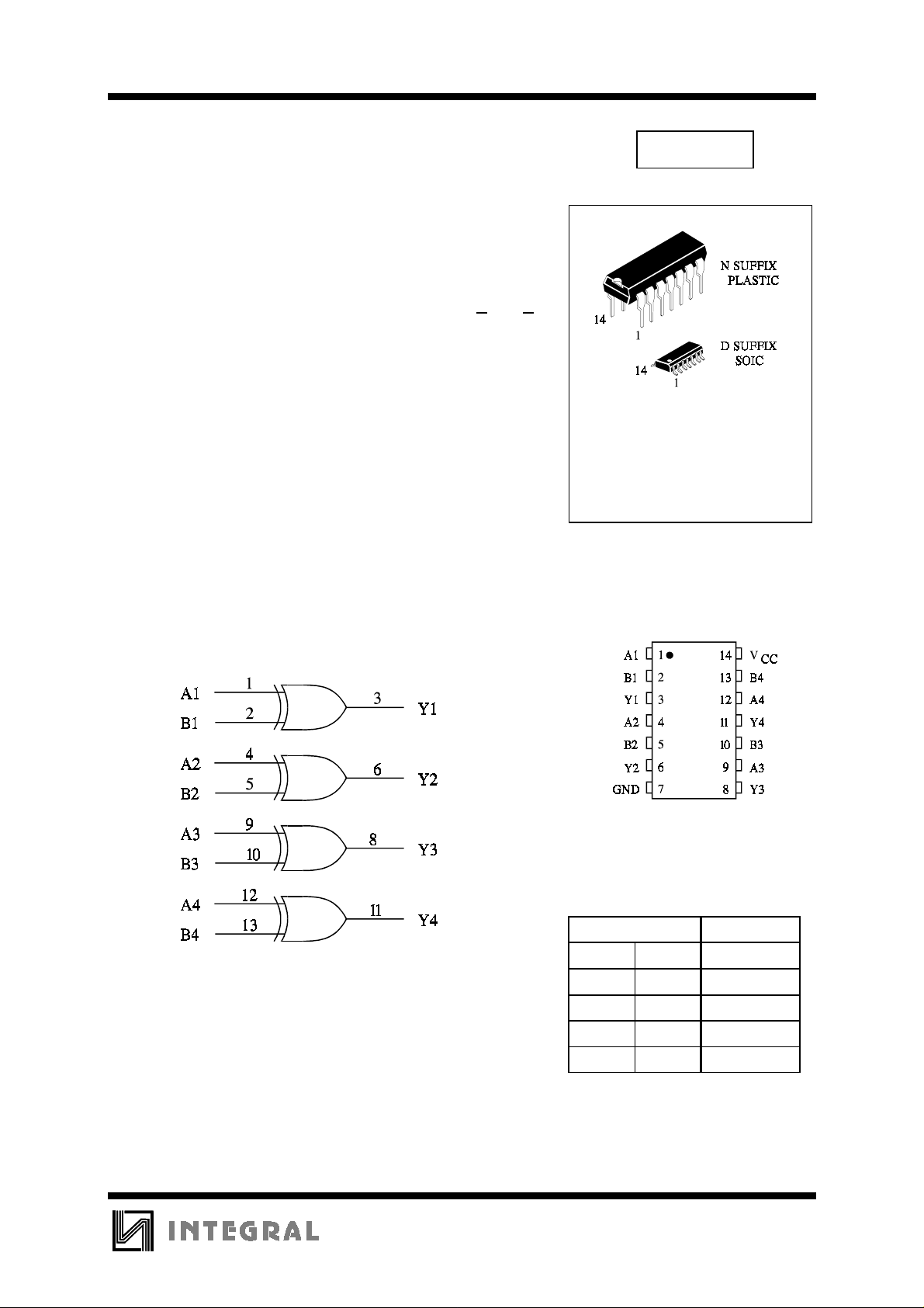
This device cont ains four i ndepe ndent 2-inp ut Exclusi ve-OR gates.
It performs the Boolean functions Y=A ⊕ B=AB+AB in positive
logic.
TECHNICAL DATA
IN74LS86
ORDERING INFORMATION
IN74LS86N Plastic
IN74LS86D SOIC
TA = 0° to 70° C for all
packages
LOGIC DIAGRAM
PIN 14 =V
PIN 7 = GND
CC
PIN ASSIGNMENT
FUNCTION TABLE
Inputs Output
AB Y
LL L
LH H
HL H
HH L
1
IN74LS86
MAXIMUM RATINGS
*
Symbol Parameter Value Unit
V
CC
V
V
OUT
Supply Voltage 7.0 V
Input Voltage 7.0 V
IN
Output Voltage 5.5 V
Tstg Storage Temperature Range -65 to +150
*
Maximum Ratings are those values beyond which damage to the device may occur.
Functional operation should be restricted to the Recommended Operating Conditions.
RECOMMENDED OPERATING CONDITIONS
Symbol Parameter Min Max Unit
V
CC
V
IH
V
IL
I
OH
I
OL
T
A
Supply Voltage 4.75 5.25 V
High Level Input Voltage 2.0 V
Low Level Input Voltage 0.8 V
High Level Output Current -0.4 mA
Low Level Output Current 8.0 mA
Ambient Temperature Range 0 +70
°
C
°
C
DC ELECTRICAL CHARACTERISTICS
over full operating conditions
Guaranteed Limit
Symbol Parameter Test Conditions Min Max Uni
t
V
V
OH
V
OL
Input Clamp Voltage VCC = min, IIN = -18 mA -1.5 V
IK
High Level Output Voltage VCC = min, IOH = -0.4 mA 2.7 V
Low Level Output Voltage VCC = min, IOL = 4 mA 0.4 V
VCC = min, IOL = 8 mA 0.5
I
IH
High Level Input Current VCC = max, VIN = 2.7 V 40
µ
A
VCC = max, VIN = 7.0 V 0.2 mA
I
IL
I
O
Low Level Input Current VCC = max, VIN = 0.4 V -0.8 mA
Output Short Circuit Current VCC = max, VO = 0 V
-20 -100 mA
(Note 1)
I
CC
Supply Current Total with
VCC = max 10 mA
outputs high
Total with
15
outputs low
Note 1: Not more than one output should be shorted at a time, and duration should not exceed one second.
2
 Loading...